JP2018056561A - Method for forming dielectric film and method for fabricating semiconductor device - Google Patents
Method for forming dielectric film and method for fabricating semiconductor deviceDownload PDFInfo
- Publication number
- JP2018056561A JP2018056561AJP2017180106AJP2017180106AJP2018056561AJP 2018056561 AJP2018056561 AJP 2018056561AJP 2017180106 AJP2017180106 AJP 2017180106AJP 2017180106 AJP2017180106 AJP 2017180106AJP 2018056561 AJP2018056561 AJP 2018056561A
- Authority
- JP
- Japan
- Prior art keywords
- forming
- film
- dielectric film
- silicon nitride
- semiconductor device
- Prior art date
- Legal status (The legal status is an assumption and is not a legal conclusion. Google has not performed a legal analysis and makes no representation as to the accuracy of the status listed.)
- Granted
Links
Images


Classifications
- H—ELECTRICITY
- H01—ELECTRIC ELEMENTS
- H01L—SEMICONDUCTOR DEVICES NOT COVERED BY CLASS H10
- H01L21/00—Processes or apparatus adapted for the manufacture or treatment of semiconductor or solid state devices or of parts thereof
- H01L21/02—Manufacture or treatment of semiconductor devices or of parts thereof
- H01L21/02104—Forming layers
- H01L21/02107—Forming insulating materials on a substrate
- H01L21/02109—Forming insulating materials on a substrate characterised by the type of layer, e.g. type of material, porous/non-porous, pre-cursors, mixtures or laminates
- H01L21/02112—Forming insulating materials on a substrate characterised by the type of layer, e.g. type of material, porous/non-porous, pre-cursors, mixtures or laminates characterised by the material of the layer
- H01L21/02123—Forming insulating materials on a substrate characterised by the type of layer, e.g. type of material, porous/non-porous, pre-cursors, mixtures or laminates characterised by the material of the layer the material containing silicon
- H01L21/0217—Forming insulating materials on a substrate characterised by the type of layer, e.g. type of material, porous/non-porous, pre-cursors, mixtures or laminates characterised by the material of the layer the material containing silicon the material being a silicon nitride not containing oxygen, e.g. SixNy or SixByNz
- H—ELECTRICITY
- H01—ELECTRIC ELEMENTS
- H01L—SEMICONDUCTOR DEVICES NOT COVERED BY CLASS H10
- H01L21/00—Processes or apparatus adapted for the manufacture or treatment of semiconductor or solid state devices or of parts thereof
- H01L21/02—Manufacture or treatment of semiconductor devices or of parts thereof
- H01L21/02104—Forming layers
- H01L21/02107—Forming insulating materials on a substrate
- H01L21/02225—Forming insulating materials on a substrate characterised by the process for the formation of the insulating layer
- H01L21/0226—Forming insulating materials on a substrate characterised by the process for the formation of the insulating layer formation by a deposition process
- H01L21/02263—Forming insulating materials on a substrate characterised by the process for the formation of the insulating layer formation by a deposition process deposition from the gas or vapour phase
- H01L21/02271—Forming insulating materials on a substrate characterised by the process for the formation of the insulating layer formation by a deposition process deposition from the gas or vapour phase deposition by decomposition or reaction of gaseous or vapour phase compounds, i.e. chemical vapour deposition
- H01L21/0228—Forming insulating materials on a substrate characterised by the process for the formation of the insulating layer formation by a deposition process deposition from the gas or vapour phase deposition by decomposition or reaction of gaseous or vapour phase compounds, i.e. chemical vapour deposition deposition by cyclic CVD, e.g. ALD, ALE, pulsed CVD
- C—CHEMISTRY; METALLURGY
- C23—COATING METALLIC MATERIAL; COATING MATERIAL WITH METALLIC MATERIAL; CHEMICAL SURFACE TREATMENT; DIFFUSION TREATMENT OF METALLIC MATERIAL; COATING BY VACUUM EVAPORATION, BY SPUTTERING, BY ION IMPLANTATION OR BY CHEMICAL VAPOUR DEPOSITION, IN GENERAL; INHIBITING CORROSION OF METALLIC MATERIAL OR INCRUSTATION IN GENERAL
- C23C—COATING METALLIC MATERIAL; COATING MATERIAL WITH METALLIC MATERIAL; SURFACE TREATMENT OF METALLIC MATERIAL BY DIFFUSION INTO THE SURFACE, BY CHEMICAL CONVERSION OR SUBSTITUTION; COATING BY VACUUM EVAPORATION, BY SPUTTERING, BY ION IMPLANTATION OR BY CHEMICAL VAPOUR DEPOSITION, IN GENERAL
- C23C16/00—Chemical coating by decomposition of gaseous compounds, without leaving reaction products of surface material in the coating, i.e. chemical vapour deposition [CVD] processes
- C23C16/04—Coating on selected surface areas, e.g. using masks
- C23C16/045—Coating cavities or hollow spaces, e.g. interior of tubes; Infiltration of porous substrates
- C—CHEMISTRY; METALLURGY
- C23—COATING METALLIC MATERIAL; COATING MATERIAL WITH METALLIC MATERIAL; CHEMICAL SURFACE TREATMENT; DIFFUSION TREATMENT OF METALLIC MATERIAL; COATING BY VACUUM EVAPORATION, BY SPUTTERING, BY ION IMPLANTATION OR BY CHEMICAL VAPOUR DEPOSITION, IN GENERAL; INHIBITING CORROSION OF METALLIC MATERIAL OR INCRUSTATION IN GENERAL
- C23C—COATING METALLIC MATERIAL; COATING MATERIAL WITH METALLIC MATERIAL; SURFACE TREATMENT OF METALLIC MATERIAL BY DIFFUSION INTO THE SURFACE, BY CHEMICAL CONVERSION OR SUBSTITUTION; COATING BY VACUUM EVAPORATION, BY SPUTTERING, BY ION IMPLANTATION OR BY CHEMICAL VAPOUR DEPOSITION, IN GENERAL
- C23C16/00—Chemical coating by decomposition of gaseous compounds, without leaving reaction products of surface material in the coating, i.e. chemical vapour deposition [CVD] processes
- C23C16/22—Chemical coating by decomposition of gaseous compounds, without leaving reaction products of surface material in the coating, i.e. chemical vapour deposition [CVD] processes characterised by the deposition of inorganic material, other than metallic material
- C23C16/30—Deposition of compounds, mixtures or solid solutions, e.g. borides, carbides, nitrides
- C23C16/34—Nitrides
- C23C16/345—Silicon nitride
- C—CHEMISTRY; METALLURGY
- C23—COATING METALLIC MATERIAL; COATING MATERIAL WITH METALLIC MATERIAL; CHEMICAL SURFACE TREATMENT; DIFFUSION TREATMENT OF METALLIC MATERIAL; COATING BY VACUUM EVAPORATION, BY SPUTTERING, BY ION IMPLANTATION OR BY CHEMICAL VAPOUR DEPOSITION, IN GENERAL; INHIBITING CORROSION OF METALLIC MATERIAL OR INCRUSTATION IN GENERAL
- C23C—COATING METALLIC MATERIAL; COATING MATERIAL WITH METALLIC MATERIAL; SURFACE TREATMENT OF METALLIC MATERIAL BY DIFFUSION INTO THE SURFACE, BY CHEMICAL CONVERSION OR SUBSTITUTION; COATING BY VACUUM EVAPORATION, BY SPUTTERING, BY ION IMPLANTATION OR BY CHEMICAL VAPOUR DEPOSITION, IN GENERAL
- C23C16/00—Chemical coating by decomposition of gaseous compounds, without leaving reaction products of surface material in the coating, i.e. chemical vapour deposition [CVD] processes
- C23C16/44—Chemical coating by decomposition of gaseous compounds, without leaving reaction products of surface material in the coating, i.e. chemical vapour deposition [CVD] processes characterised by the method of coating
- C23C16/455—Chemical coating by decomposition of gaseous compounds, without leaving reaction products of surface material in the coating, i.e. chemical vapour deposition [CVD] processes characterised by the method of coating characterised by the method used for introducing gases into reaction chamber or for modifying gas flows in reaction chamber
- C23C16/45523—Pulsed gas flow or change of composition over time
- C23C16/45525—Atomic layer deposition [ALD]
- C23C16/45553—Atomic layer deposition [ALD] characterized by the use of precursors specially adapted for ALD
- H—ELECTRICITY
- H01—ELECTRIC ELEMENTS
- H01L—SEMICONDUCTOR DEVICES NOT COVERED BY CLASS H10
- H01L21/00—Processes or apparatus adapted for the manufacture or treatment of semiconductor or solid state devices or of parts thereof
- H01L21/02—Manufacture or treatment of semiconductor devices or of parts thereof
- H01L21/02104—Forming layers
- H01L21/02107—Forming insulating materials on a substrate
- H01L21/02109—Forming insulating materials on a substrate characterised by the type of layer, e.g. type of material, porous/non-porous, pre-cursors, mixtures or laminates
- H01L21/02112—Forming insulating materials on a substrate characterised by the type of layer, e.g. type of material, porous/non-porous, pre-cursors, mixtures or laminates characterised by the material of the layer
- H01L21/02123—Forming insulating materials on a substrate characterised by the type of layer, e.g. type of material, porous/non-porous, pre-cursors, mixtures or laminates characterised by the material of the layer the material containing silicon
- H01L21/02164—Forming insulating materials on a substrate characterised by the type of layer, e.g. type of material, porous/non-porous, pre-cursors, mixtures or laminates characterised by the material of the layer the material containing silicon the material being a silicon oxide, e.g. SiO2
- H—ELECTRICITY
- H01—ELECTRIC ELEMENTS
- H01L—SEMICONDUCTOR DEVICES NOT COVERED BY CLASS H10
- H01L21/00—Processes or apparatus adapted for the manufacture or treatment of semiconductor or solid state devices or of parts thereof
- H01L21/02—Manufacture or treatment of semiconductor devices or of parts thereof
- H01L21/02104—Forming layers
- H01L21/02107—Forming insulating materials on a substrate
- H01L21/02109—Forming insulating materials on a substrate characterised by the type of layer, e.g. type of material, porous/non-porous, pre-cursors, mixtures or laminates
- H01L21/02205—Forming insulating materials on a substrate characterised by the type of layer, e.g. type of material, porous/non-porous, pre-cursors, mixtures or laminates the layer being characterised by the precursor material for deposition
- H01L21/02208—Forming insulating materials on a substrate characterised by the type of layer, e.g. type of material, porous/non-porous, pre-cursors, mixtures or laminates the layer being characterised by the precursor material for deposition the precursor containing a compound comprising Si
- H01L21/02219—Forming insulating materials on a substrate characterised by the type of layer, e.g. type of material, porous/non-porous, pre-cursors, mixtures or laminates the layer being characterised by the precursor material for deposition the precursor containing a compound comprising Si the compound comprising silicon and nitrogen
- H01L21/02222—Forming insulating materials on a substrate characterised by the type of layer, e.g. type of material, porous/non-porous, pre-cursors, mixtures or laminates the layer being characterised by the precursor material for deposition the precursor containing a compound comprising Si the compound comprising silicon and nitrogen the compound being a silazane
- H—ELECTRICITY
- H01—ELECTRIC ELEMENTS
- H01L—SEMICONDUCTOR DEVICES NOT COVERED BY CLASS H10
- H01L21/00—Processes or apparatus adapted for the manufacture or treatment of semiconductor or solid state devices or of parts thereof
- H01L21/02—Manufacture or treatment of semiconductor devices or of parts thereof
- H01L21/02104—Forming layers
- H01L21/02107—Forming insulating materials on a substrate
- H01L21/02225—Forming insulating materials on a substrate characterised by the process for the formation of the insulating layer
- H01L21/0226—Forming insulating materials on a substrate characterised by the process for the formation of the insulating layer formation by a deposition process
- H01L21/02263—Forming insulating materials on a substrate characterised by the process for the formation of the insulating layer formation by a deposition process deposition from the gas or vapour phase
- H01L21/02271—Forming insulating materials on a substrate characterised by the process for the formation of the insulating layer formation by a deposition process deposition from the gas or vapour phase deposition by decomposition or reaction of gaseous or vapour phase compounds, i.e. chemical vapour deposition
- H01L21/02274—Forming insulating materials on a substrate characterised by the process for the formation of the insulating layer formation by a deposition process deposition from the gas or vapour phase deposition by decomposition or reaction of gaseous or vapour phase compounds, i.e. chemical vapour deposition in the presence of a plasma [PECVD]
- H—ELECTRICITY
- H01—ELECTRIC ELEMENTS
- H01L—SEMICONDUCTOR DEVICES NOT COVERED BY CLASS H10
- H01L21/00—Processes or apparatus adapted for the manufacture or treatment of semiconductor or solid state devices or of parts thereof
- H01L21/02—Manufacture or treatment of semiconductor devices or of parts thereof
- H01L21/02104—Forming layers
- H01L21/02107—Forming insulating materials on a substrate
- H01L21/02296—Forming insulating materials on a substrate characterised by the treatment performed before or after the formation of the layer
- H01L21/02299—Forming insulating materials on a substrate characterised by the treatment performed before or after the formation of the layer pre-treatment
- H01L21/02301—Forming insulating materials on a substrate characterised by the treatment performed before or after the formation of the layer pre-treatment in-situ cleaning
- H—ELECTRICITY
- H01—ELECTRIC ELEMENTS
- H01L—SEMICONDUCTOR DEVICES NOT COVERED BY CLASS H10
- H01L21/00—Processes or apparatus adapted for the manufacture or treatment of semiconductor or solid state devices or of parts thereof
- H01L21/02—Manufacture or treatment of semiconductor devices or of parts thereof
- H01L21/02104—Forming layers
- H01L21/02365—Forming inorganic semiconducting materials on a substrate
- H01L21/02518—Deposited layers
- H01L21/02521—Materials
- H01L21/02538—Group 13/15 materials
- H01L21/0254—Nitrides
- H—ELECTRICITY
- H01—ELECTRIC ELEMENTS
- H01L—SEMICONDUCTOR DEVICES NOT COVERED BY CLASS H10
- H01L21/00—Processes or apparatus adapted for the manufacture or treatment of semiconductor or solid state devices or of parts thereof
- H01L21/02—Manufacture or treatment of semiconductor devices or of parts thereof
- H01L21/04—Manufacture or treatment of semiconductor devices or of parts thereof the devices having potential barriers, e.g. a PN junction, depletion layer or carrier concentration layer
- H01L21/18—Manufacture or treatment of semiconductor devices or of parts thereof the devices having potential barriers, e.g. a PN junction, depletion layer or carrier concentration layer the devices having semiconductor bodies comprising elements of Group IV of the Periodic Table or AIIIBV compounds with or without impurities, e.g. doping materials
- H01L21/28—Manufacture of electrodes on semiconductor bodies using processes or apparatus not provided for in groups H01L21/20 - H01L21/268
- H01L21/28008—Making conductor-insulator-semiconductor electrodes
- H01L21/28017—Making conductor-insulator-semiconductor electrodes the insulator being formed after the semiconductor body, the semiconductor being silicon
- H01L21/28158—Making the insulator
- H01L21/28167—Making the insulator on single crystalline silicon, e.g. using a liquid, i.e. chemical oxidation
- H01L21/28194—Making the insulator on single crystalline silicon, e.g. using a liquid, i.e. chemical oxidation by deposition, e.g. evaporation, ALD, CVD, sputtering, laser deposition
- H—ELECTRICITY
- H01—ELECTRIC ELEMENTS
- H01L—SEMICONDUCTOR DEVICES NOT COVERED BY CLASS H10
- H01L21/00—Processes or apparatus adapted for the manufacture or treatment of semiconductor or solid state devices or of parts thereof
- H01L21/02—Manufacture or treatment of semiconductor devices or of parts thereof
- H01L21/04—Manufacture or treatment of semiconductor devices or of parts thereof the devices having potential barriers, e.g. a PN junction, depletion layer or carrier concentration layer
- H01L21/18—Manufacture or treatment of semiconductor devices or of parts thereof the devices having potential barriers, e.g. a PN junction, depletion layer or carrier concentration layer the devices having semiconductor bodies comprising elements of Group IV of the Periodic Table or AIIIBV compounds with or without impurities, e.g. doping materials
- H01L21/30—Treatment of semiconductor bodies using processes or apparatus not provided for in groups H01L21/20 - H01L21/26
- H01L21/302—Treatment of semiconductor bodies using processes or apparatus not provided for in groups H01L21/20 - H01L21/26 to change their surface-physical characteristics or shape, e.g. etching, polishing, cutting
- H01L21/306—Chemical or electrical treatment, e.g. electrolytic etching
- H01L21/30604—Chemical etching
- H—ELECTRICITY
- H01—ELECTRIC ELEMENTS
- H01L—SEMICONDUCTOR DEVICES NOT COVERED BY CLASS H10
- H01L21/00—Processes or apparatus adapted for the manufacture or treatment of semiconductor or solid state devices or of parts thereof
- H01L21/70—Manufacture or treatment of devices consisting of a plurality of solid state components formed in or on a common substrate or of parts thereof; Manufacture of integrated circuit devices or of parts thereof
- H01L21/71—Manufacture of specific parts of devices defined in group H01L21/70
- H01L21/768—Applying interconnections to be used for carrying current between separate components within a device comprising conductors and dielectrics
- H01L21/76801—Applying interconnections to be used for carrying current between separate components within a device comprising conductors and dielectrics characterised by the formation and the after-treatment of the dielectrics, e.g. smoothing
- H01L21/76829—Applying interconnections to be used for carrying current between separate components within a device comprising conductors and dielectrics characterised by the formation and the after-treatment of the dielectrics, e.g. smoothing characterised by the formation of thin functional dielectric layers, e.g. dielectric etch-stop, barrier, capping or liner layers
- H01L21/76831—Applying interconnections to be used for carrying current between separate components within a device comprising conductors and dielectrics characterised by the formation and the after-treatment of the dielectrics, e.g. smoothing characterised by the formation of thin functional dielectric layers, e.g. dielectric etch-stop, barrier, capping or liner layers in via holes or trenches, e.g. non-conductive sidewall liners
- H—ELECTRICITY
- H10—SEMICONDUCTOR DEVICES; ELECTRIC SOLID-STATE DEVICES NOT OTHERWISE PROVIDED FOR
- H10B—ELECTRONIC MEMORY DEVICES
- H10B43/00—EEPROM devices comprising charge-trapping gate insulators
- H10B43/30—EEPROM devices comprising charge-trapping gate insulators characterised by the memory core region
- H—ELECTRICITY
- H10—SEMICONDUCTOR DEVICES; ELECTRIC SOLID-STATE DEVICES NOT OTHERWISE PROVIDED FOR
- H10D—INORGANIC ELECTRIC SEMICONDUCTOR DEVICES
- H10D64/00—Electrodes of devices having potential barriers
- H10D64/01—Manufacture or treatment
- H10D64/031—Manufacture or treatment of data-storage electrodes
- H10D64/037—Manufacture or treatment of data-storage electrodes comprising charge-trapping insulators
Landscapes
- Engineering & Computer Science (AREA)
- Chemical & Material Sciences (AREA)
- Physics & Mathematics (AREA)
- Condensed Matter Physics & Semiconductors (AREA)
- General Physics & Mathematics (AREA)
- Manufacturing & Machinery (AREA)
- Computer Hardware Design (AREA)
- Microelectronics & Electronic Packaging (AREA)
- Power Engineering (AREA)
- Chemical Kinetics & Catalysis (AREA)
- General Chemical & Material Sciences (AREA)
- Materials Engineering (AREA)
- Mechanical Engineering (AREA)
- Metallurgy (AREA)
- Organic Chemistry (AREA)
- Inorganic Chemistry (AREA)
- Plasma & Fusion (AREA)
- Crystallography & Structural Chemistry (AREA)
- Formation Of Insulating Films (AREA)
- Chemical Vapour Deposition (AREA)
- Semiconductor Memories (AREA)
- Electrodes Of Semiconductors (AREA)
- Non-Volatile Memory (AREA)
- Insulated Gate Type Field-Effect Transistor (AREA)
- Internal Circuitry In Semiconductor Integrated Circuit Devices (AREA)
Abstract
Translated fromJapaneseDescription
Translated fromJapanese本発明は、誘電膜の形成方法及びこれを用いた半導体装置の製造方法に関し、特に、工程効率を向上させた誘電膜の形成方法及びこれを用いた半導体装置の製造方法に関する。 The present invention relates to a dielectric film forming method and a semiconductor device manufacturing method using the same, and more particularly to a dielectric film forming method with improved process efficiency and a semiconductor device manufacturing method using the same.
半導体装置の高集積化に伴い、半導体素子を製造することが非常に難しくなってきている。
特に、半導体装置の製造に用いられる薄膜は、例えば、シリコン窒化膜などを基板上にステップカバレッジ(step coverage)を有するように形成することが非常に難しくなってきている。With the high integration of semiconductor devices, it has become very difficult to manufacture semiconductor elements.
In particular, it has become very difficult for a thin film used for manufacturing a semiconductor device to form, for example, a silicon nitride film or the like on a substrate so as to have step coverage.
一方、BTBAS(Bis(Tertiary−Butylamine)Silane)などの有機系シリコン前駆体を用いたALD(Atomic Layer Deposition)法によってシリコン窒化膜を形成する場合、ステップカバレッジは向上できるものの、有機系シリコン前駆体に含まれているC、N成分などにより形成されたシリコン窒化膜の膜質が劣化するおそれがあるという問題点がある。 On the other hand, when a silicon nitride film is formed by an ALD (Atomic Layer Deposition) method using an organic silicon precursor such as BTBAS (Bis (Tertiary-Butylamine) Silane), although the step coverage can be improved, the organic silicon precursor is improved. There is a problem that the quality of the silicon nitride film formed by the C, N component, etc. contained in the film may deteriorate.
本発明は上記従来の半導体装置の薄膜製造における問題点に鑑みてなされたものであって、本発明の目的は、WER(wet etch rate)が相対的に減少したALD法を用いてシリコン窒化膜を形成することにより工程効率を向上させた、誘電膜の形成方法を提供することにある。
また、本発明の他の目的は、WERが相対的に減少したALD法を用いてシリコン窒化膜を形成することにより工程効率を向上させた、半導体装置の製造方法を提供することにある。The present invention has been made in view of the problems in the above-described conventional thin film manufacturing of a semiconductor device, and an object of the present invention is to use a silicon nitride film using an ALD method in which WER (wet etch rate) is relatively reduced. It is an object of the present invention to provide a method for forming a dielectric film, in which process efficiency is improved by forming.
Another object of the present invention is to provide a method for manufacturing a semiconductor device, in which process efficiency is improved by forming a silicon nitride film using an ALD method in which WER is relatively reduced.
上記目的を達成するためになされた本発明による誘電膜の形成方法は、チャンバー内に基板を提供する段階と、前記基板上にALD(Atomic Layer Deposition)法を用いてシリコン窒化膜を形成するする段階と、を有し、前記シリコン窒化膜を形成する段階は、前記チャンバー内へ、HCDZ(Hexachlorodisilazane)を含むシリコン前駆体を含む第1ガス、及び窒素成分を含む第2ガスを提供することを含むことを特徴とする。 In order to achieve the above object, a method for forming a dielectric film according to the present invention includes providing a substrate in a chamber and forming a silicon nitride film on the substrate using an ALD (Atomic Layer Deposition) method. And forming the silicon nitride film includes providing a first gas containing a silicon precursor containing HCDZ (Hexachlorodisilazane) and a second gas containing a nitrogen component into the chamber. It is characterized by including.
上記目的を達成するためになされた本発明による半導体装置の製造方法は、基板上に段差が形成された構造体を形成する段階と、前記構造体上にALD(Atomic Layer Deposition)法を用いて誘電膜構造体を形成する段階と、をさらに有し、前記誘電膜構造体を形成する段階は、シリコン窒化物を含む第1誘電膜を形成する段階を含み、前記第1誘電膜を形成する段階は、一つのチャンバー内で、インサイチュ(in−situ)にて、HCDZ(Hexachlorodisilazane)を含むシリコン前駆体を含む第1ガスを提供する段階を含むことを特徴とする。 In order to achieve the above object, a method of manufacturing a semiconductor device according to the present invention includes a step of forming a structure having a step on a substrate, and an ALD (Atomic Layer Deposition) method on the structure. Forming a dielectric film structure, and forming the dielectric film structure includes forming a first dielectric film including silicon nitride, and forming the first dielectric film. The step includes providing a first gas including a silicon precursor including HCDZ (Hexachlorodisilazane) in-situ in one chamber.
本発明に係る誘電膜の形成方法及び半導体装置の製造方法によれば、HCDZ(Hexachlorodisilazane)をシリコン前駆体として用いて生成されたシリコン窒化膜は、相対的に小さい厚さで、既存のHCDS(hexachlorodisilane)をシリコン前駆体として用いて生成されたシリコン窒化膜と同じ膜質特性を持ち、その結果、既存のHCDSをシリコン前駆体として用いてシリコン窒化膜を形成する場合よりも工程時間が相対的に減少するので、工程効率を向上させることができるという効果がある。 According to the method for forming a dielectric film and the method for manufacturing a semiconductor device according to the present invention, a silicon nitride film formed using HCDZ (Hexachlorodisilazane) as a silicon precursor has a relatively small thickness, and has an existing HCDS ( Hexachlorodisilane) has the same film quality characteristics as a silicon nitride film generated as a silicon precursor, and as a result, the process time is relatively longer than when a silicon nitride film is formed using an existing HCDS as a silicon precursor. Since it decreases, there exists an effect that process efficiency can be improved.
次に、本発明に係る誘電膜の形成方法及び半導体装置の製造方法を実施するための形態の具体例を図面を参照しながら説明する。 Next, specific examples of modes for carrying out the dielectric film forming method and the semiconductor device manufacturing method according to the present invention will be described with reference to the drawings.
他の定義がない限り、本明細書で使用されるすべての用語(技術及び科学的用語を含む)は、本発明の属する技術分野における通常の知識を有する者に共通して理解できる意味で使用できるであろう。また、一般に使用される辞典に定義されている用語は、明白に特に定義されていない限り、理想的又は過度に解釈されない。 Unless otherwise defined, all terms used herein (including technical and scientific terms) are used in a meaning that is commonly understood by those having ordinary knowledge in the technical field to which this invention belongs. It will be possible. Also, terms defined in commonly used dictionaries are not to be interpreted ideally or unduly unless explicitly defined otherwise.
以下、図1を参照して、本発明の幾つかの実施形態に係るシリコン窒化膜の形成方法について説明する。
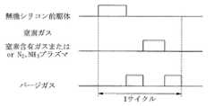
図1は、本発明の一実施形態に係るシリコン窒化膜の形成方法を説明するためのタイミング図である。Hereinafter, a method for forming a silicon nitride film according to some embodiments of the present invention will be described with reference to FIG.
FIG. 1 is a timing diagram for explaining a method of forming a silicon nitride film according to an embodiment of the present invention.
本発明の技術的思想に基づくシリコン窒化膜の形成は、ALD法を用いてインサイチュ(in−situ)で形成される。
ALD(Atomic Layer Deposition)法は、シリコン前駆体を含む第1ガスを供給する第1段階と、反応していない第1ガスを第1パージガスを用いて除去する第2段階と、窒化ガスを含む第2ガスを供給して原子層レベルのシリコン窒化膜を形成する第3段階と、反応していない第2ガスを第2パージガスを用いて除去する第4段階とを含む。The silicon nitride film based on the technical idea of the present invention is formed in-situ using the ALD method.
An ALD (Atomic Layer Deposition) method includes a first stage for supplying a first gas containing a silicon precursor, a second stage for removing unreacted first gas using a first purge gas, and a nitriding gas. It includes a third stage in which a second gas is supplied to form an atomic layer level silicon nitride film, and a fourth stage in which the unreacted second gas is removed using a second purge gas.
具体的に、図1を参照すると、まず、反応チャンバー内に、シリコン窒化膜が形成されるべき対象体(具体的に、基板上に形成された構造体)を配置させる。
この場合、基板上に形成された構造体の幅に対する高さの比であるアスペクト比は、10以上であり得る。
但し、本発明の技術的思想はこれに制限されるものではない。Specifically, referring to FIG. 1, first, an object (specifically, a structure formed on a substrate) on which a silicon nitride film is to be formed is placed in a reaction chamber.
In this case, the aspect ratio, which is the ratio of the height to the width of the structure formed on the substrate, can be 10 or more.
However, the technical idea of the present invention is not limited to this.
次いで、適正の温度及び圧力を調節した後、シリコン前駆体を含む第1ガスをチャンバー内に供給する。
すると、対象体上にシリコン前駆体が吸着する。
ここで、シリコン前駆体は、C、N成分を含む有機系シリコン前駆体とは異なり、C、N成分を含まない化合物であり得る。
但し、本発明の技術的思想はこれに制限されるものではない。すなわち、他の幾つかの実施形態において、シリコン前駆体はC成分を含むことができる。Next, after adjusting an appropriate temperature and pressure, a first gas containing a silicon precursor is supplied into the chamber.
Then, the silicon precursor is adsorbed on the object.
Here, unlike the organic silicon precursor containing C and N components, the silicon precursor may be a compound not containing C and N components.
However, the technical idea of the present invention is not limited to this. That is, in some other embodiments, the silicon precursor can include a C component.
シリコン前駆体は、例えば、以下の化学式1で示すHCDZ(Hexachlorodisilazane)を含むことができる。
HCDZをシリコン前駆体として使用する場合は、HCDS(hexachlorodisilane)をシリコン前駆体として使用する場合よりもWER(wet etch rate)が減少できる。
ここで、WERは、DHF(Diluted HF)、すなわち、脱イオン水(DI water)を用いて希釈されたフッ酸(HF)に対するエッチング率を意味する。When HCDZ is used as a silicon precursor, WER (wet etch rate) can be reduced as compared with the case where HCDS (hexachlorodisilane) is used as a silicon precursor.
Here, WER means an etching rate with respect to DHF (Diluted HF), that is, hydrofluoric acid (HF) diluted with deionized water (DI water).
すなわち、HCDZをシリコン前駆体として用いて生成されたシリコン窒化膜は、HCDSをシリコン前駆体として用いて生成されたシリコン窒化膜よりもエッチング物質に対するエッチング率が相対的に小さい。
これにより、HCDZをシリコン前駆体として用いて生成されたシリコン窒化膜は、相対的に小さい厚さで、HCDSをシリコン前駆体として用いて生成されたシリコン窒化膜と同じ膜質特性を持つことができる。
その結果、本発明の技術的思想に基づくHCDZをシリコン前駆体として用いてシリコン窒化膜を形成する場合は、既存のHCDSをシリコン前駆体として用いてシリコン窒化膜を形成する場合よりも工程時間が相対的に減少するので、工程効率を向上させることができる。That is, a silicon nitride film generated using HCDZ as a silicon precursor has a relatively lower etching rate with respect to an etching substance than a silicon nitride film generated using HCDS as a silicon precursor.
Accordingly, a silicon nitride film generated using HCDZ as a silicon precursor can have the same film quality characteristics as a silicon nitride film generated using HCDS as a silicon precursor with a relatively small thickness. .
As a result, when forming a silicon nitride film using HCDZ based on the technical idea of the present invention as a silicon precursor, the process time is longer than when forming a silicon nitride film using existing HCDS as a silicon precursor. Since it decreases relatively, process efficiency can be improved.
次いで、チャンバー内へ第1パージガス、例えば、N2、He又はArガスを供給して、チャンバー内に残留する(又は未反応)のシリコンソース前駆体を除去する。
すると、対象体上に吸着したシリコン前駆体が原子層レベルで薄く形成される。
その後、チャンバー内へ窒素成分を含む窒化ガスを供給してシリコン窒化膜を形成する。
ここで、窒化ガスは、窒素(N2)、アンモニア(NH3)及び一酸化窒素(NO)の内の少なくとも一つを含むことができる。
但し、本発明の技術的思想はこれに制限されるものではない。Next, a first purge gas such as N2 , He, or Ar gas is supplied into the chamber to remove the remaining (or unreacted) silicon source precursor in the chamber.
Then, the silicon precursor adsorbed on the object is thinly formed at the atomic layer level.
Thereafter, a nitride gas containing a nitrogen component is supplied into the chamber to form a silicon nitride film.
Here, the nitriding gas may include at least one of nitrogen (N2 ), ammonia (NH3 ), and nitric oxide (NO).
However, the technical idea of the present invention is not limited to this.
続いて、チャンバー内へ第2パージガス、例えばN2、He又はArガスを供給して、チャンバー内に残留する窒化ガスを除去する。
その後、1サイクルのシリコン窒化膜形成工程が完成し、対象体上に原子層レベルのシリコン窒化膜が形成される。
その後、上記の工程を繰り返し行うことにより、対象体上に適切な厚さのシリコン窒化膜を形成することができる。Subsequently, a second purge gas such as N2 , He, or Ar gas is supplied into the chamber to remove the nitriding gas remaining in the chamber.
Thereafter, a one-cycle silicon nitride film forming step is completed, and an atomic layer level silicon nitride film is formed on the object.
Thereafter, the silicon nitride film having an appropriate thickness can be formed on the object by repeatedly performing the above steps.
次いで、シリコン窒化膜の膜質を向上させるために、対象体上に適切な厚さで形成されたシリコン窒化膜を熱処理する。
ここで、熱処理は、例えば、他のCVD(Chemical Vapor Deposition)窒化膜と同じ蒸着温度で850℃〜1050℃で行って膜質を向上させることができる。
但し、本発明の技術的思想はこれに制限されるものではない。
これにより形成されたシリコン窒化膜は、CVD法などによって形成されたシリコン窒化膜に比べて膜質が向上できる。
本発明の技術的思想に基づいて形成されたシリコン窒化膜は、ステップカバレッジが良いので、段差のある構造体、又はアスペクト比(aspect ratio)の大きい構造体上にボイドなくコンフォーマルに形成できる。Next, in order to improve the film quality of the silicon nitride film, the silicon nitride film formed with an appropriate thickness on the object is heat-treated.
Here, the heat treatment can be performed, for example, at 850 ° C. to 1050 ° C. at the same vapor deposition temperature as other CVD (Chemical Vapor Deposition) nitride films to improve the film quality.
However, the technical idea of the present invention is not limited to this.
The silicon nitride film thus formed can improve the film quality as compared with the silicon nitride film formed by the CVD method or the like.
Since the silicon nitride film formed based on the technical idea of the present invention has good step coverage, it can be formed conformally without voids on a stepped structure or a structure having a large aspect ratio.
本発明に関するより詳細な内容は、以下の具体的な実験例によって説明し、ここに記載されていない内容は、この技術分野における熟練した者であれば十分に技術的に類推することができるので、説明を省略する。
以下、図2及び図3を参照して、本発明の実施形態に係るシリコン窒化膜の形成に関連する実験例を説明する。More detailed contents of the present invention will be explained by the following specific experimental examples, and contents not described here can be sufficiently technically analogized by those skilled in the art. The description is omitted.
Hereinafter, with reference to FIGS. 2 and 3, an experimental example related to the formation of the silicon nitride film according to the embodiment of the present invention will be described.
図2及び図3は、本発明の一実施形態に係るシリコン窒化膜の形成に関連する実験例を説明するためのグラフである。 2 and 3 are graphs for explaining experimental examples related to formation of a silicon nitride film according to an embodiment of the present invention.
≪実験例−HCDZとHCDSの工程温度によるWERの測定≫
下記のような実験例及び比較例に対して実験を行った。
実験例では、HCDZを使用するALD法を用いてシリコン窒化膜を形成した。
これに対し、比較例では、HCDSを使用するALD法を用いてシリコン窒化膜を形成した。
図2を参照すると、実験例に基づいて工程温度400℃、450℃及び500℃それぞれでHCDZを用いてシリコン窒化膜を形成し、比較例に基づいて工程温度400℃、450℃及び500℃それぞれでHCDSを用いてシリコン窒化膜を形成した。≪Experimental example-Measurement of WER by HCDZ and HCDS process temperature≫
Experiments were conducted on the following experimental examples and comparative examples.
In the experimental example, a silicon nitride film was formed using an ALD method using HCDZ.
On the other hand, in the comparative example, the silicon nitride film was formed using the ALD method using HCDS.
Referring to FIG. 2, a silicon nitride film is formed using HCDZ at process temperatures of 400 ° C., 450 ° C., and 500 ° C. based on an experimental example, and process temperatures of 400 ° C., 450 ° C., and 500 ° C. based on a comparative example, respectively. Then, a silicon nitride film was formed using HCDS.
グラフb1、b2及びb3は、実験例に基づいて工程温度400℃、450℃及び500℃それぞれでHCDZを用いてシリコン窒化膜を形成するときのWER(wet etch rate)を示す。
また、グラフa1、a2及びa3は、比較例に基づいて工程温度400℃、450℃及び500℃それぞれでHCDSを用いてシリコン窒化膜を形成するときのWERを示す。
図2に示す「WER」は、脱イオン水(DI water)を用いて200:1の比率で希釈されたフッ酸(HF)に対するエッチング率を意味する。Graphs b1, b2 and b3 show WER (wet etch rate) when a silicon nitride film is formed using HCDZ at process temperatures of 400 ° C., 450 ° C. and 500 ° C. based on experimental examples.
Graphs a1, a2, and a3 show WERs when a silicon nitride film is formed using HCDS at process temperatures of 400 ° C., 450 ° C., and 500 ° C., respectively, based on the comparative example.
“WER” shown in FIG. 2 means an etching rate with respect to hydrofluoric acid (HF) diluted at a ratio of 200: 1 using deionized water (DI water).
グラフa1及びb1を参照すると、400℃でシリコン窒化膜を形成する場合には、比較例に基づいてHCDSを用いる方よりも、実験例に基づいてHCDZを用いる方が低いWERを示すことが分かる。
また、グラフa2及びb2を参照すると、450℃でシリコン窒化膜を形成する場合には、比較例に基づいてHCDSを用いる方よりも、実験例に基づいてHCDZを用いる方が低いWERを示すことが分かる。
また、グラフa3及びb3を参照すると、500℃でシリコン窒化膜を形成する場合には、比較例に基づいてHCDSを用いる方よりも、実験例に基づいてHCDZを用いる方が低いWERを示すことが分かる。Referring to graphs a1 and b1, it can be seen that when a silicon nitride film is formed at 400 ° C., the WCDZ based on the experimental example shows a lower WER than the HCDS based on the comparative example. .
Referring to graphs a2 and b2, when forming a silicon nitride film at 450 ° C., WCDZ based on the experimental example shows lower WER than using HCDS based on the comparative example. I understand.
Also, referring to graphs a3 and b3, when forming a silicon nitride film at 500 ° C., WCDZ based on the experimental example shows a lower WER than using HCDS based on the comparative example. I understand.
具体的には、500℃でHCDSを用いる場合には、WERは4.5nm/min以上であり、図2に示すように、略4.9nm/min程度のWERを有する。
しかし、500℃でHCDZを用いる場合には、WERは4.5nm/min未満であり、図2に示すように、略4.2nm/min程度のWERを有することが分かる。
その結果、実験例に基づいてHCDZを用いてシリコン窒化膜を形成する場合には、4.5nm/min未満のWERを有することが分かる。
また、HCDSを用いる方とは異なり、HCDZを用いることにより相対的にWERが減少し、これにより、相対的に小さい厚さで、HCDSをシリコン前駆体として用いて生成されたシリコン窒化膜と同じ膜質特性を持つことができる。Specifically, when HCDS is used at 500 ° C., the WER is 4.5 nm / min or more, and has a WER of about 4.9 nm / min as shown in FIG.
However, when HCDZ is used at 500 ° C., the WER is less than 4.5 nm / min, and as shown in FIG. 2, it can be seen that the WER is about 4.2 nm / min.
As a result, it can be seen that when a silicon nitride film is formed using HCDZ based on an experimental example, the WER is less than 4.5 nm / min.
Also, unlike the case of using HCDS, the WER is relatively reduced by using HCDZ, which is the same as the silicon nitride film formed using HCDS as a silicon precursor with a relatively small thickness. Can have film quality characteristics.
≪実験例−HCDZとHCDSの工程温度によるGPCの測定≫
下記のような実験例及び比較例に対して実験を行った。
実験例では、HCDZを使用するALD法を用いてシリコン窒化膜を形成した。
これに対し、比較例では、HCDSを使用するALD法を用いてシリコン窒化膜を形成した。
図3を参照すると、実験例に基づいて工程温度400℃、450℃及び500℃それぞれでHCDZを用いてシリコン窒化膜を形成し、比較例に基づいて工程温度400℃、450℃及び500℃それぞれでHCDSを用いてシリコン窒化膜を形成した。≪Experimental example-GPC measurement by process temperature of HCDZ and HCDS≫
Experiments were conducted on the following experimental examples and comparative examples.
In the experimental example, a silicon nitride film was formed using an ALD method using HCDZ.
On the other hand, in the comparative example, the silicon nitride film was formed using the ALD method using HCDS.
Referring to FIG. 3, a silicon nitride film is formed using HCDZ at process temperatures of 400 ° C., 450 ° C., and 500 ° C. based on the experimental example, and process temperatures of 400 ° C., 450 ° C., and 500 ° C. based on the comparative example, respectively. Then, a silicon nitride film was formed using HCDS.
グラフb4、b5及びb6は、実験例に基づいて工程温度400℃、450℃及び500℃それぞれでHCDZを用いてシリコン窒化膜を形成するときのGPC(growth per cycle)を示す。
また、グラフa4、a5及びa6は、比較例に基づいて工程温度400℃、450℃及び500℃それぞれでHCDSを用いてシリコン窒化膜を形成するときのGPCを示す。Graphs b4, b5, and b6 show GPC (growth per cycle) when a silicon nitride film is formed using HCDZ at process temperatures of 400 ° C., 450 ° C., and 500 ° C., respectively, based on experimental examples.
Graphs a4, a5, and a6 show GPC when a silicon nitride film is formed using HCDS at process temperatures of 400 ° C., 450 ° C., and 500 ° C. based on the comparative example.
グラフa4及びb4を参照すると、400℃でシリコン窒化膜を形成する場合には、比較例に基づいてHCDSを用いる方よりも、実験例に基づいてHCDZを用いる方が低いGPCを示すことが分かる。
また、グラフa5及びb5を参照すると、450℃でシリコン窒化膜を形成する場合には、比較例に基づいてHCDSを用いる方よりも、実験例に基づいてHCDZを用いる方が低いGPCを示すことが分かる。
但し、グラフa6及びb6を参照すると、500℃でシリコン窒化膜を形成する場合には、比較例に基づいてHCDSを用いる方と、実験例に基づいてHCDZを用いる方とが実質的に同一のGPCを示すことが分かる。Referring to graphs a4 and b4, it can be seen that when forming a silicon nitride film at 400 ° C., using HCDZ based on the experimental example shows lower GPC than using HCDS based on the comparative example. .
Also, referring to graphs a5 and b5, when forming a silicon nitride film at 450 ° C., GPC is lower when HCDZ is used based on the experimental example than when HCDS is used based on the comparative example. I understand.
However, referring to graphs a6 and b6, when the silicon nitride film is formed at 500 ° C., the method using HCDS based on the comparative example and the method using HCDZ based on the experimental example are substantially the same. It can be seen that GPC is indicated.
その結果、図2及び図3を参照すると、500℃でシリコン窒化膜を形成する場合には、比較例に基づいてHCDSを用いる方と、実験例に基づいてHCDZを用いる方とが実質的に同一のGPCを示し、比較例に基づいてHCDSを用いる方よりも、実験例に基づいてHCDZを用いる方が低いWERを示すことが分かる。
すなわち、HCDSを用いる方とは異なり、HCDZを用いることにより、同じ工程時間の間に、膜質特性に優れたシリコン窒化膜を形成することができることが分かる。
言い換えれば、HCDSを用いることとは異なり、HCDZを用いることにより、同じ膜質特性を有するシリコン窒化膜を形成するための工程時間が相対的に減少して工程効率が向上できることが分かる。As a result, referring to FIG. 2 and FIG. 3, when the silicon nitride film is formed at 500 ° C., there are substantially a method using HCDS based on the comparative example and a method using HCDZ based on the experimental example. It can be seen that the same GPC is shown, and that the WCDZ based on the experimental example shows a lower WER than the HCDS based on the comparative example.
That is, it can be seen that, unlike the case of using HCDS, by using HCDZ, a silicon nitride film having excellent film quality characteristics can be formed during the same process time.
In other words, it can be seen that, unlike using HCDS, using HCDZ can relatively reduce the process time for forming a silicon nitride film having the same film quality characteristics and improve the process efficiency.
次に、図4〜図6を参照して、本発明の一実施形態に係る半導体装置の製造方法を説明する。
図4〜図6は、本発明の一実施形態に係る半導体装置の製造方法を説明するための図であり、具体的には、図4〜図6は、フラッシュメモリ装置の製造方法に関連する工程中間段階を示す断面図である。Next, with reference to FIGS. 4-6, the manufacturing method of the semiconductor device which concerns on one Embodiment of this invention is demonstrated.
4 to 6 are views for explaining a method of manufacturing a semiconductor device according to an embodiment of the present invention. Specifically, FIGS. 4 to 6 relate to a method of manufacturing a flash memory device. It is sectional drawing which shows a process intermediate | middle stage.
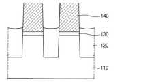
図4を参照すると、基板110上にトンネル絶縁膜130及び電荷貯蔵膜140を順次形成する。
トンネル絶縁膜130は、電荷のトンネリングに対するエネルギーバンドギャップを提供し、例えば、シリコン酸化物、シリコン窒化物又は高誘電率物質(high−k material)を含むことができる。
ここで、高誘電率物質は、ハフニウム酸化物、アルミニウム酸化物、ハフニウムアルミニウム酸化物、ジルコニウム酸化物などの金属酸化物などを含むことができるが、本発明の技術的思想はこれに制限されるものではない。
例えば、トンネル絶縁膜130は、誘電定数(dielectric constatnt)だけでなく、エネルギーバンドギャップ(energy bandgap)性質を考慮して、様々な物質で形成できる。Referring to FIG. 4, a
The
Here, the high dielectric constant material may include metal oxides such as hafnium oxide, aluminum oxide, hafnium aluminum oxide, and zirconium oxide, but the technical idea of the present invention is limited thereto. It is not a thing.
For example, the
電荷貯蔵膜140は、電荷を貯蔵する役目をする。
このような電荷貯蔵膜は、例えば、フラッシュメモリ装置がフローティングゲート型である場合には、ポリシリコン膜のような導電性物質で形成でき、フラッシュメモリ装置が電荷トラップ型である場合には、シリコン窒化物、ハフニウム酸化物、ジルコニウム酸化物、タンタル酸化物、ハフニウム窒化酸化物、ハフニウムシリコン酸化物、タングステンドープドアルミニウム酸化物、ナノドットなどで形成できる。The
Such a charge storage film can be formed of a conductive material such as a polysilicon film when the flash memory device is a floating gate type, and silicon when the flash memory device is a charge trap type. Nitride, hafnium oxide, zirconium oxide, tantalum oxide, hafnium nitride oxide, hafnium silicon oxide, tungsten-doped aluminum oxide, nanodots, or the like can be used.
ここで、トンネル絶縁膜130及び電荷貯蔵膜140を形成することは、例えば、基板110上にプレ(pre)トンネル絶縁膜、プレ電荷貯蔵膜及びマスク膜を順次形成し、プレトンネル絶縁膜、プレ電荷貯蔵膜及びマスク膜をパターニングして素子分離膜120を形成した後、マスク膜を除去することを含み得る。
しかし、本発明の技術的思想はこれに制限されるものではなく、トンネル絶縁膜130及び電荷貯蔵膜140を形成することは様々な他の方法によって実施し得ることを、本発明の属する技術分野における当業者であれば理解することができるであろう。Here, the
However, the technical idea of the present invention is not limited to this, and it is possible to form the
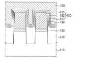
図5及び図6を参照すると、電荷貯蔵膜140上に、シリコン酸化物で形成された第1誘電膜151、シリコン酸化物とは異なる物質で形成された第2誘電膜152、及びシリコン酸化物で形成された第3誘電膜153を含む誘電膜構造体150を、上述した本発明の技術的思想に基づくALD法を用いて形成する。
ここで、誘電膜構造体150は、フラッシュメモリ装置がフローティングゲート型である場合にはゲート間誘電膜であり、フラッシュメモリ装置が電荷トラップ型である場合にはブロッキング誘電膜であり得る。Referring to FIGS. 5 and 6, the
Here, the dielectric film structure 150 may be an inter-gate dielectric film when the flash memory device is a floating gate type, and may be a blocking dielectric film when the flash memory device is a charge trap type.
以下、第2誘電膜152をシリコン窒化膜として誘電膜構造体150をインサイチュ(in−situ)で形成する場合を例示的に説明する。
まず、チャンバー内に、電荷貯蔵膜140が形成された段差(あるいは凹凸)を有する半導体基板110を配置する。
その後、シリコン酸化物を含む第1誘電膜151を形成する。
次いで、適正の温度及び圧力を調節した後、シリコンソース前駆体を含む第1ガスをチャンバー内へ供給する。
すると、第1誘電膜151上にシリコン前駆体が吸着する。
ここで、シリコンソース前駆体は、上述したように、例えば、HCDZを用いる。Hereinafter, a case where the dielectric film structure 150 is formed in-situ using the second dielectric film 152 as a silicon nitride film will be described as an example.
First, the
Thereafter, a
Next, after adjusting an appropriate temperature and pressure, a first gas containing a silicon source precursor is supplied into the chamber.
Then, the silicon precursor is adsorbed on the
Here, as described above, for example, HCDZ is used as the silicon source precursor.
その後、上述したように、第1パージガス、第2ガス及び第2パージガスを順次供給して、第1誘電膜151上に、シリコン窒化物を含む原子層レベルの第2誘電膜152を形成する。
上記の工程を繰り返し行うことにより、第1誘電膜151上に適正厚さのシリコン窒化膜からなる第2誘電膜152を形成する。
続いて、第2誘電膜152上に、シリコン酸化物を含む第3誘電膜153を形成する。Thereafter, as described above, the first purge gas, the second gas, and the second purge gas are sequentially supplied to form the second dielectric film 152 at the atomic layer level including silicon nitride on the
By repeating the above steps, a second dielectric film 152 made of a silicon nitride film having an appropriate thickness is formed on the
Subsequently, a third
これにより形成された誘電膜構造体150は、ステップカバレッジが良いので、アスペクト比の大きい、例えば、アスペクト比が10以上である電荷貯蔵膜140間のスペースにボイドなくコンフォーマルに形成することができる。
また、第1〜第3誘電膜(151、152、153)をインサイチュにて形成するので、工程時間が減るなど、工程を簡単にすることができる。
次いで、誘電膜構造体150上にコントロールゲート160を形成する。
コントロールゲート160は、例えば、ポリシリコンで形成されるか、或いは金属電極物質、例えばTaN、TiN、WN及びWを含むグループから選択された一つ又はその組み合わせで形成できる。Since the dielectric film structure 150 thus formed has good step coverage, it can be formed conformally without voids in the space between the
Further, since the first to third dielectric films (151, 152, 153) are formed in situ, the process can be simplified, for example, the process time can be reduced.
Next, a
The
次に、図7〜図9を参照して、本発明の他の実施形態に係る半導体装置の製造方法を説明する。
図7〜図9は、本発明の他の実施形態に係る半導体装置の製造方法を説明するための図であり、具体的には、図7は、DRAMセル領域のレイアウト図であり、図8、9は、DRAMセルの半導体装置の製造方法に関連する工程中間段階を示す断面図である。Next, with reference to FIGS. 7-9, the manufacturing method of the semiconductor device which concerns on other embodiment of this invention is demonstrated.
7 to 9 are views for explaining a method of manufacturing a semiconductor device according to another embodiment of the present invention. Specifically, FIG. 7 is a layout diagram of a DRAM cell region, and FIG. , 9 are cross-sectional views showing intermediate stages of processes related to a method of manufacturing a semiconductor device of a DRAM cell.
図7を参照すると、DRAMセル領域のレイアウト図が示される。
基板の活性領域210を、ゲート230が水平方向に通り過ぎ、GBL(global bit line)240が垂直方向に通り過ぎる。
基板の活性領域210以外の部分は、素子分離領域220である。Referring to FIG. 7, a layout diagram of the DRAM cell region is shown.
Through the
A portion other than the
図8及び図9を参照すると、メモリセル領域が示される。
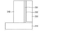
半導体基板の活性領域210上に、ビットラインとなるGBL240を形成する。
続いて、GBL240を形成した後、GBL240の側壁に、シリコン酸化物を含む第1誘電膜251を形成する。
この場合、第1誘電膜251はスペーサーの機能を行うことができる。
次いで、第1誘電膜251上に、シリコン窒化物を含む第2誘電膜252を形成する。
この場合、第2誘電膜252は、上述した本発明に基づくALD法を用いて形成する。8 and 9, a memory cell region is shown.
A
Subsequently, after forming the
In this case, the
Next, a
In this case, the
具体的には、第2誘電膜252を形成することは、適正の温度及び圧力を調節した後、シリコンソース前駆体を含む第1ガスをチャンバー内へ供給する。
すると、第1誘電膜251上にシリコン前駆体が吸着する。
ここで、シリコンソース前駆体は、上述したように、例えばHCDZを用いる。
続いて、上述したように、第1パージガス、第2ガス及び第2パージガスを順次供給して、第1誘電膜251上に、シリコン窒化物を含む原子層レベルの第2誘電膜252を形成する。
この場合、第2ガスとシリコン前駆体との反応は、熱(Thermal)及びプラズマ(Plasma)で励起させて反応させることができる。
上記の工程を繰り返し行うことにより、第1誘電膜251上に、適正厚さのシリコン窒化膜からなる第2誘電膜252を形成する。Specifically, forming the
Then, the silicon precursor is adsorbed on the
Here, as described above, for example, HCDZ is used as the silicon source precursor.
Subsequently, as described above, the first purge gas, the second gas, and the second purge gas are sequentially supplied to form the
In this case, the reaction between the second gas and the silicon precursor may be caused to react by being excited by heat and plasma.
By repeating the above process, a
次いで、第2誘電膜252上に、シリコン酸化物を含む第3誘電膜253を形成する。
セル領域には、不純物層の形成が不要であるため、セル領域を覆う感光液パターン(図示せず)を形成する。
感光液パターン(図示せず)を除去し、第3誘電膜253を除去した後、第2誘電膜252を異方性エッチングして窒化膜スペーサーを作り、基板の活性領域210と接する第2誘電膜252を除去する。Next, a third
Since it is not necessary to form an impurity layer in the cell region, a photosensitive solution pattern (not shown) that covers the cell region is formed.
After removing the photoresist pattern (not shown) and removing the third
次に、図10〜図13を参照して、本発明のさらに他の実施形態に係る半導体装置の製造方法を説明する。
図10〜図13は、本発明のさらに他の実施形態に係る半導体装置の製造方法を説明するための図であり、具体的には、図10〜図13は、積層ナノシートトランジスタ構造を有する半導体装置の製造方法に関連する工程中間段階を示す断面図である。Next, with reference to FIGS. 10-13, the manufacturing method of the semiconductor device which concerns on further another embodiment of this invention is demonstrated.
10 to 13 are views for explaining a method of manufacturing a semiconductor device according to still another embodiment of the present invention. Specifically, FIGS. 10 to 13 illustrate a semiconductor having a stacked nanosheet transistor structure. It is sectional drawing which shows the process intermediate | middle stage relevant to the manufacturing method of an apparatus.
図10を参照すると、基板310上に、犠牲層321及び半導体層322が交互に積層された積層構造体320を形成する。
積層構造体320のうち、基板310と接する犠牲層321は、例えばウェハーボンディング(wafer bonding)方式などによって、基板310に接合された層であり得るが、本発明の技術的思想はこれらに限定されるものではない。Referring to FIG. 10, a
The
基板310と接する犠牲層321上に、半導体層322と犠牲層321を交互に形成する。
犠牲層321と半導体層322は、例えば、エピタキシャル成長(epitaxial growth)方法を用いて形成できるが、本発明の技術的思想はこれに制限されるものではない。
積層構造体320の最上層は、例えば、犠牲層321であり得るが、本発明の技術的思想はこれに制限されるものではない。Semiconductor layers 322 and
The
The uppermost layer of the
犠牲層321と半導体層322は、互いに異なる物質を含むことができる。
犠牲層321と半導体層322は、互いに異なるエッチング選択比を有する物質を含むことができる。
犠牲層321は、例えば、SiGe又はGeのうちのいずれかを含むことができるが、本発明の技術的思想はこれに制限されるものではない。
半導体層322は、例えば、Si又はIII−V族化合物半導体のうちのいずれかを含むことができるが、本発明の技術的思想はこれに制限されるものではない。The
The
The
The
次いで、積層構造体320上に、第1方向Xに延びる第1マスクパターン(図11の符号341)を形成する。
第1マスクパターン(図11の符号341)は、例えば、シリコン酸化膜、シリコン窒化膜及びシリコン酸化窒化膜の内の少なくとも一つを含む物質で形成できる。
第1マスクパターン341がシリコン窒化膜を含む場合には、第1マスクパターン341は、上述した本発明の技術的思想に基づくALD法を用いて形成できる。Next, a first mask pattern (
For example, the first mask pattern (
When the
具体的に、第1マスクパターン341を形成することは、適正の温度及び圧力を調節した後、シリコンソース前駆体を含む第1ガスをチャンバー内に供給する。
すると、積層構造体320上にシリコン前駆体が吸着する。
ここで、シリコンソース前駆体は、上述したように、例えばHCDZを用いる。
続いて、上述したように、第1パージガス、第2ガス及び第2パージガスを順次供給して、積層構造体320上に、シリコン窒化物を含む原子層レベルの第1マスクパターン341を形成する。
上記の工程を繰り返し行うことにより、積層構造体320上に、適正厚さのシリコン窒化膜からなる第1マスクパターン341を形成する。In detail, the
Then, the silicon precursor is adsorbed on the
Here, as described above, for example, HCDZ is used as the silicon source precursor.
Subsequently, as described above, the first purge gas, the second gas, and the second purge gas are sequentially supplied to form the atomic layer level
By repeating the above steps, a
図11を参照すると、第1マスクパターン341をマスクとして用いて積層構造体320をエッチングして、半導体パターン構造体330を形成する。
例えば、積層構造体320を基板310の上面が露出するまでエッチングすることにより、半導体パターン構造体330を形成する。
半導体パターン構造体330は、第1方向Xに長く延長する。
また、半導体パターン構造体330は、基板310上に交互に積層された複数の犠牲層及び複数の半導体層を含む。Referring to FIG. 11, the
For example, the
The
The
すなわち、半導体パターン構造体330は、基板310上に形成された第1犠牲層331と、第1犠牲層331上に形成された第1半導体層334と、第1半導体層334上に形成された第2犠牲層332と、第2犠牲層332上に形成された第2半導体層335と、第2半導体層335上に形成された第3犠牲層333とを含むことができる。
また、積層構造体320をエッチングするとき、基板310の一部もエッチングしてアクティブ領域ARを形成することができる。
また、基板310と第1マスクパターン341を覆うように層間絶縁膜を形成した後、第1マスクパターン341の上面が露出するまで平坦化工程を行うことにより、図11の層間絶縁膜351を形成する。
続いて、半導体パターン構造体330上に位置する第1のマスクパターン341を除去する。That is, the
Further, when the
Further, after an interlayer insulating film is formed so as to cover the
Subsequently, the
図12を参照すると、第2マスクパターン342を用いてエッチング工程を行い、半導体パターン構造体330と交差して、第1方向X及び第2方向Zに対して垂直な第3方向に延長されるゲート絶縁膜353及び犠牲ゲート360を形成する。
第2マスクパターン342は、例えば、シリコン酸化膜、シリコン窒化膜及びシリコン酸化窒化膜の内の少なくとも一つを含む物質で形成できる。
第2マスクパターン342がシリコン窒化膜を含む場合、第2マスクパターン342は、上述した本発明の技術的思想に基づくALD法を用いて形成できる。
これにより、犠牲ゲート360は、半導体パターン構造体330上に形成される。
また、ゲート絶縁膜353は、それぞれ絶縁膜352の側壁及び上面とフィールド絶縁膜354の上面に沿って形成する。Referring to FIG. 12, an etching process is performed using the
For example, the
When the
As a result, the
Further, the
ここで、半導体パターン構造体330を覆うように絶縁膜352を形成することができ、絶縁膜352は、半導体パターン構造体330とゲート絶縁膜353との間に形成できる。
ここで、絶縁膜352は、例えば、酸化膜であってもよく、より具体的には、SiO2を含むことができるが、本発明の技術的思想はこれに制限されるものではない。
ゲート絶縁膜353は、シリコン酸化膜であってもよく、犠牲ゲート360は、ポリシリコン又はアモルファスシリコンの内のいずれかであり得るが、本発明の技術的思想はこれに制限されるものではない。Here, the insulating
Here, the insulating
The
図13を参照すると、犠牲ゲート360の側壁にゲートスペーサ370とダミーゲートスペーサ380を形成する。
具体的には、犠牲ゲート360と半導体パターン構造体330を覆うスペーサー膜を基板310上に形成する。
スペーサー膜がシリコン窒化物を含む場合、スペーサー膜は、上述した本発明の技術的思想に基づくALD法を用いて形成できる。
具体的には、スペーサー膜を形成することは、適正の温度及び圧力を調節した後、シリコンソース前駆体を含む第1ガスをチャンバー内に供給する。
すると、犠牲ゲート360と半導体パターン構造体330上にシリコン前駆体が吸着する。ここで、シリコンソース前駆体は、上述したように、例えばHCDZを用いることができる。Referring to FIG. 13, a
Specifically, a spacer film that covers the
When the spacer film contains silicon nitride, the spacer film can be formed by using the ALD method based on the technical idea of the present invention described above.
Specifically, forming a spacer film supplies a first gas containing a silicon source precursor into the chamber after adjusting an appropriate temperature and pressure.
Then, the silicon precursor is adsorbed on the
次いで、上述したように、第1パージガス、第2ガス及び第2パージガスを順次供給して、犠牲ゲート360と半導体パターン構造体330上に、シリコン窒化物を含む原子層レベルのスペーサー膜を形成する。
上記の工程を繰り返し行うことにより、犠牲ゲート360と半導体パターン構造体330上に、適正厚さのシリコン窒化膜からなるスペーサー膜を形成する。
続いて、スペーサー膜にエッチバック(etch−back)して、犠牲ゲート360の側壁にゲートスペーサ370とダミーゲートスペーサ380を形成する。Next, as described above, the first purge gas, the second gas, and the second purge gas are sequentially supplied to form an atomic layer level spacer film including silicon nitride on the
By repeating the above steps, a spacer film made of a silicon nitride film having an appropriate thickness is formed on the
Subsequently, etch back is performed on the spacer film, and a
次に、図14及び図15を参照して、本発明のまたさらに他の実施形態に係る半導体装置の製造方法を説明する。
図14及び図15は、本発明のまたさらに実施形態に係る半導体装置の製造方法を説明するための図であり、具体的には、図14及び図15は、コンタクト内にスペーサーが形成された半導体装置の製造方法に関連する工程中間段階を示す断面図である。Next, with reference to FIGS. 14 and 15, a method for manufacturing a semiconductor device according to still another embodiment of the present invention will be described.
14 and 15 are views for explaining a method of manufacturing a semiconductor device according to still another embodiment of the present invention. Specifically, FIGS. 14 and 15 show spacers formed in the contacts. It is sectional drawing which shows the process intermediate | middle stage relevant to the manufacturing method of a semiconductor device.
図14を参照すると、第1ゲートパターンと第2ゲートパターンは、基板410上に互いに離隔して形成する。
ここで、第1ゲートパターンと第2ゲートパターンは実質的に同一の構成を含む。
第1及び第2ゲートパターンそれぞれは、ゲートスペーサ450、絶縁膜パターン420、ゲート電極パターン430、及びキャッピングパターン440を含む。
絶縁膜パターン420は、インターフェース膜421とゲート絶縁膜422を含むことができる。Referring to FIG. 14, the first gate pattern and the second gate pattern are formed apart from each other on the
Here, the first gate pattern and the second gate pattern include substantially the same configuration.
Each of the first and second gate patterns includes a
The insulating
インターフェース膜421は、基板410とゲート絶縁膜422との間の不良界面を防止する役目をする。
インターフェース膜421は、誘電率9以下の低誘電物質層、例えば、シリコン酸化膜(kは約4)又はシリコン酸窒化膜(酸素原子及び窒素原子の含有量に応じて、kは約4〜8)を含むことができる。
インターフェース膜421は、例えば、化学的酸化方法、紫外線酸化(UV oxidation)方法、又はデュアルプラズマ酸化(Dual Plasma oxidation)方法などを用いて形成できる。The
The
The
ゲート絶縁膜422は、インターフェース膜421上に形成する。
但し、インターフェース膜421が存在しない場合に、ゲート絶縁膜422は基板410上に形成できる。
ゲート絶縁膜422は、高誘電率(high−k)を有する物質を含むことができる。The
However, the
The
ゲート絶縁膜422は、例えば、ハフニウム酸化物(hafnium oxide)、ハフニウムシリコン酸化物(hafnium silicon oxide)、ランタン酸化物(lanthanum oxide)、ランタンアルミニウム酸化物(lanthanum aluminum oxide)、ジルコニウム酸化物(zirconium oxide)、ジルコニウムシリコン酸化物(zirconium silicon oxide)、タンタル酸化物(tantalum oxide)、チタン酸化物(titanium oxide)、バリウムストロンチウムチタン酸化物(barium strontium titanium oxide)、バリウムチタン酸化物(barium titanium oxide)、ストロンチウムチタン酸化物(strontium titanium oxide)、イットリウム酸化物(yttrium oxide)、アルミニウム酸化物(Aluminum oxide)、鉛スカンジウムタンタル酸化物(lead scandium tantalum oxide)、及び鉛亜鉛ニオブ酸塩(lead zinc niobate)の内の少なくとも一つを含むことができるが、本発明の技術的思想はこれに制限されるものではない。 The
一方、ゲート絶縁膜422は、形成しようとする素子の種類に応じて適切な厚さに形成する。
例えば、ゲート絶縁膜422が、HfO2である場合、ゲート絶縁膜422は約50Å以下(約5Å〜50Å)の厚さに形成できるが、本発明の技術的思想はこれに制限されるものではない。On the other hand, the
For example, when the
ゲート電極パターン430は、仕事関数調節膜431とゲートメタル432を含む。
仕事関数調節膜431は、ゲート絶縁膜422上に形成する。
仕事関数調節膜431は、ゲート絶縁膜422と接触して形成する。
仕事関数調節膜431は、仕事関数の調節のために使用される。
仕事関数調節膜431は、例えば、メタル窒化物を含むことができる。
仕事関数調節膜431は、半導体装置のタイプに応じて異なる物質を含むことができる。The
The work
The work
The work
The work
The work
p型仕事関数調節膜は、例えば、TiN、WN、TaN、Ru、及びこれらの組み合わせの内の少なくとも一つを含むことができるが、本発明の技術的思想はこれに制限されるものではない。
また、n型仕事関数調節膜は、例えば、Ti、Ag、Al、TiAl、TiAlN、TiAlC、TaC、TaCN、TaSiN、Mn、Zr及びこれらの組み合わせのうち少なくとも一つを含むことができるが、本発明の技術的思想はこれに制限されるものではない。
また、p型仕事関数調節膜は、例えば、TiNからなる単一膜、又はTiN下部膜とTaN上部膜からなる二重膜などから構成できるが、本発明の技術的思想はこれに制限されるものではない。The p-type work function adjusting film may include, for example, at least one of TiN, WN, TaN, Ru, and combinations thereof, but the technical idea of the present invention is not limited thereto. .
Further, the n-type work function adjusting film can include, for example, at least one of Ti, Ag, Al, TiAl, TiAlN, TiAlC, TaC, TaCN, TaSiN, Mn, Zr, and combinations thereof. The technical idea of the invention is not limited to this.
The p-type work function adjusting film can be composed of, for example, a single film made of TiN or a double film made of a TiN lower film and a TaN upper film, but the technical idea of the present invention is limited to this. It is not a thing.
ゲートメタル432は、仕事関数調節膜431上に形成する。
ゲートメタル432は、図に示す如く、仕事関数調節膜431と接触して形成する。
すなわち、ゲートメタル432は、仕事関数調節膜431によって生成された空間を埋めるように形成する。
ゲートメタル432は、導電性を有する物質、例えば、W又はAlを含むことができるが、本発明の技術的思想はこれに制限されるものではない。The
As shown in the figure, the
That is, the
The
キャッピングパターン440は、ゲートメタル432上に形成する。
キャッピングパターン440は、図に示す如く、ゲートメタル432と接触して形成する。
キャッピングパターン440は、例えば、シリコン酸化物(SiN)、シリコン酸窒化物(SiON)、シリコン酸化物(SiO2)、シリコン炭窒化物(SiCN)、シリコン炭化酸窒化物(SiOCN)及びこれらの組み合わせの内の少なくとも一つを含むことができる。The
The
The
層間絶縁膜460は、基板410上に形成され、第1ゲートパターンと第2ゲートパターンを覆うように形成する。
層間絶縁膜460は、例えば、低誘電率物質、酸化膜、窒化膜及び酸窒化膜の内の少なくとも一つを含むことができる。The
The
低誘電率物質は、例えば、FOX(Flowable Oxide)、TOSZ(Tonen SilaZen)、USG(Undoped Silica Glass)、BSG(Borosilica Glass)、PSG(PhosphoSilaca Glass)、BPSG(BoroPhosphoSilica Glass)、PETEOS(Plasma Enhanced Tetra Ethyl Ortho Silicate)、FSG(Fluoride Silicate Glass)、CDO(Carbon Doped silicon Oxide)、キセロゲル(Xerogel)、エアロゲル(Aerogel)、アモルファスフッ素化カーボン(Amorphous Fluorinated Carbon)、OSG(Organo Silicate Glass)、パリレン(Parylene)、BCB(bis−benzocyclobutenes)、SiLK、ポリイミド(polyimide)、多孔性高分子材料(porous polymeric material)、及びこれらの組み合わせを含むことができるが、本発明の技術的思想はこれに制限されるものではない。 Low dielectric constant materials include, for example, FOX (Flowable Oxide), TOSZ (Tonen SilaZen), USG (Unloaded Silica Glass), BSG (Borosica Glass), PSG (Phossilica Glass), BPSG (BoSlaP) Ethyl Ortho Silicate, FSG (Fluoride Silicate Glass), CDO (Carbon Doped Silicon Oxide), Xerogel, Aerogel, Amorphous Fluoro Carbon (Amorphous Fluoro Carbon) ), OSG (Organic Silicate Glass), Parylene, BCB (bis-benzocycles), SiLK, polyimide, porous polymeric material, and combinations thereof. The technical idea of the present invention is not limited to this.
第1及び第2ゲートパターンが基板410上に形成された後、第1及び第2ゲートパターンを覆う層間絶縁膜460を形成する。
続いて、第1ゲートパターンと第2ゲートパターンとの間の基板410を露出させるように層間絶縁膜460内にトレンチTを形成する。
層間絶縁膜460内にトレンチTを形成することは、例えば、ドライエッチング工程、ウェットエッチング工程、又はこれらの組み合わせで層間絶縁膜460の一部を除去して実現することができる。After the first and second gate patterns are formed on the
Subsequently, a trench T is formed in the
Forming the trench T in the
図15を参照すると、トレンチT内の側壁にスペーサー物質470をコンフォーマルに形成する。
スペーサー物質470がシリコン窒化膜を含む場合には、スペーサー物質470は、上述した本発明の技術的思想に基づくALD法を用いて形成できる。
具体的には、トレンチT内の側壁にスペーサー物質470を形成することは、適正の温度及び圧力を調節した後、シリコンソース前駆体を含む第1ガスをチャンバー内に供給する。
すると、トレンチT上にシリコン前駆体が吸着する。ここで、シリコンソース前駆体は、上述したように、例えばHCDZを用いる。Referring to FIG. 15, the
When the
Specifically, forming the
Then, the silicon precursor is adsorbed on the trench T. Here, as described above, for example, HCDZ is used as the silicon source precursor.
続いて、上述したように、第1パージガス、第2ガス及び第2パージガスを順次供給して、トレンチT上に、シリコン窒化物を含む原子層レベルのスペーサー物質470をコンフォーマルに形成する。
上述の工程を繰り返し行うことにより、トレンチT上に、適正厚さのシリコン窒化膜からなるコンタクトスペーサーを形成する。Subsequently, as described above, the first purge gas, the second gas, and the second purge gas are sequentially supplied to form the atomic layer
By repeating the above steps, a contact spacer made of a silicon nitride film having an appropriate thickness is formed on the trench T.
図16は、本発明の一実施形態に係る半導体装置の製造方法を順次に説明するためのフローチャートである。
図16で説明する半導体装置の製造方法の一部は、図1を参照して説明したのと同一である。FIG. 16 is a flowchart for sequentially explaining a method for manufacturing a semiconductor device according to an embodiment of the present invention.
A part of the manufacturing method of the semiconductor device described in FIG. 16 is the same as that described with reference to FIG.
まず、原子層蒸着(ALD)装置の反応チャンバーに、誘電膜を形成するための対象物をロードする(ステップS10)。
対象物は、段差(あるいは凹凸)を有する構造物が形成された基板であり得る。
構造物には開口、例えばトレンチなどが定義できる。
開口は、少なくとも10のアスペクト比を有することができる。
但し、本発明の技術的思想はこれに制限されるものではない。
すなわち、他の実施形態において、構造物は開口を含まなくてもよい。
ALD装置は、反応チャンバー内の温度及び圧力などの工程条件を調節するように制御する。First, an object for forming a dielectric film is loaded into a reaction chamber of an atomic layer deposition (ALD) apparatus (step S10).
The object may be a substrate on which a structure having a step (or unevenness) is formed.
An opening, such as a trench, can be defined in the structure.
The opening can have an aspect ratio of at least 10.
However, the technical idea of the present invention is not limited to this.
That is, in other embodiments, the structure may not include an opening.
The ALD apparatus is controlled to adjust process conditions such as temperature and pressure in the reaction chamber.
次いで、ALD工程によって、前駆体を含むガスが反応チャンバー内に注入される(ステップS20)。
この場合、前駆体は、シリコン前駆体、例えば、HCDZ(hexachlorodisilazane)を含む。
続いて、パージガスを用いて、誘電膜の表面に吸着していないシリコン前駆体を含むガスを除去する(ステップS30)。Next, a gas containing a precursor is injected into the reaction chamber by the ALD process (step S20).
In this case, the precursor includes a silicon precursor, for example, HCDZ (hexachlorodisilazane).
Subsequently, a gas containing a silicon precursor not adsorbed on the surface of the dielectric film is removed using a purge gas (step S30).
その後、反応チャンバー内に、HCDZと反応する窒素ガスを注入する(ステップS40)。
これにより、対象物の表面に、シリコンを含む窒化物層が原子層レベルで形成され、その後、反応していない窒素ガスをパージガスを用いて除去する(ステップS50)。Thereafter, nitrogen gas that reacts with HCDZ is injected into the reaction chamber (step S40).
Thereby, a nitride layer containing silicon is formed at the atomic layer level on the surface of the object, and then the unreacted nitrogen gas is removed using the purge gas (step S50).
上述した工程段階(ステップS20、ステップS30、ステップS40、ステップS50)は、一つのALD工程サイクルを構成する。
次いで、所望の厚さに誘電膜が形成されたか否かの判断が行われる(ステップS60)。
誘電膜が所望の厚さに形成されていない場合(いいえ)には、上述した工程段階(ステップS20、ステップS30、ステップS40、ステップS50)のサイクルが再び行われる。
誘電膜が所望の厚さに形成された場合(はい)には、対象物を反応チャンバーから取り出す、及び/又は、誘電膜上に他の層を形成する。The above-described process steps (Step S20, Step S30, Step S40, Step S50) constitute one ALD process cycle.
Next, it is determined whether or not the dielectric film has been formed to a desired thickness (step S60).
If the dielectric film is not formed to a desired thickness (No), the above-described process steps (Step S20, Step S30, Step S40, Step S50) are performed again.
If the dielectric film is formed to a desired thickness (yes), the object is removed from the reaction chamber and / or another layer is formed on the dielectric film.
本発明に係る誘電膜の形成方法及び半導体装置の製造方法は、HCDZを含むシリコン前駆体を用いてALD法で誘電膜を形成することにより、既存の他のシリコン前駆体を使用することと比較して優れたステップカバレッジを実現することができる。
これにより、段差(あるいは凹凸)を有する構造体、又はアスペクト比(aspect ratio))の大きい構造体上にシリコン窒化膜をボイドなくコンフォーマルに形成することができる。The method of forming a dielectric film and the method of manufacturing a semiconductor device according to the present invention are compared with the use of another existing silicon precursor by forming a dielectric film by an ALD method using a silicon precursor containing HCDZ. And excellent step coverage can be realized.
Accordingly, a silicon nitride film can be formed conformally without voids on a structure having a step (or unevenness) or a structure having a large aspect ratio.
また、実験例と比較例によって詳述したように、従来の他のシリコン前駆体を使用することと比較して相対的にWERが向上し、これにより、相対的に小さい厚さで、既存の他のシリコン前駆体を使用することと実質的に同一の膜質特性を持つことができる。
その結果、本発明の技術的思想に基づくHCDZをシリコン前駆体として用いてシリコン窒化膜を形成する場合、従来のシリコン前駆体を用いてシリコン窒化膜を形成する場合よりも工程時間が相対的に減少するので、工程効率を向上させることができる。In addition, as detailed in the experimental example and the comparative example, the WER is relatively improved as compared with the use of other conventional silicon precursors. It can have substantially the same film quality characteristics as using other silicon precursors.
As a result, when forming a silicon nitride film using HCDZ based on the technical idea of the present invention as a silicon precursor, the process time is relatively longer than when forming a silicon nitride film using a conventional silicon precursor. Since it decreases, process efficiency can be improved.
以上で、本発明の技術的思想に基づくALD法を用いた誘電膜の形成方法及び半導体装置の製造方法を例示的に説明したが、本発明の技術的思想はこれに制限されるものではない。
すなわち、ALD法を用いて、シリコン窒化物を含む誘電膜をコンフォーマルに形成する他の誘電膜の形成方法及び半導体装置の製造方法に、本発明の技術的思想に基づくALD法が使用できる。The dielectric film forming method and the semiconductor device manufacturing method using the ALD method based on the technical idea of the present invention have been exemplarily described above, but the technical idea of the present invention is not limited thereto. .
That is, the ALD method based on the technical idea of the present invention can be used for another dielectric film forming method and a semiconductor device manufacturing method for forming a dielectric film containing silicon nitride conformally using the ALD method.
尚、本発明は、上述の実施形態に限られるものではない。本発明の技術的範囲から逸脱しない範囲内で多様に変更実施することが可能である。 The present invention is not limited to the embodiment described above. Various modifications can be made without departing from the technical scope of the present invention.
110、310、410 基板
120 素子分離膜
130 トンネル絶縁膜
140 電荷貯蔵膜
150 誘電膜構造体
151、251 第1誘電膜
152、252 第2誘電膜
153、253 第3誘電膜
160 コントロールゲート
210 基板の活性領域
220 素子分離領域
230 ゲート
240 GBL(global bit line)
320 積層構造体
321 犠牲層
322 半導体層
330 半導体パターン構造体
331、332、333 (第1〜第3)犠牲層
334、335 (第1、第2)半導体層
341 第1マスクパターン
342 第2マスクパターン
351、460 層間絶縁膜
352 絶縁膜
353 ゲート絶縁膜
354 フィールド絶縁膜
360 犠牲ゲート
370、450 ゲートスペーサ
380 ダミーゲートスペーサ
420 絶縁膜パターン
421 インターフェース膜
422 ゲート絶縁膜
430 ゲート電極パターン
431 仕事関数調節膜
432 ゲートメタル
440 キャッピングパターン
470 スペーサー物質
AR アクティブ領域
110, 310, 410
320
Claims (10)
Translated fromJapanese前記基板上にALD(Atomic Layer Deposition)法を用いてシリコン窒化膜を形成するする段階と、を有し、
前記シリコン窒化膜を形成する段階は、
前記チャンバー内へ、HCDZ(Hexachlorodisilazane)を含むシリコン前駆体を含む第1ガス、及び窒素成分を含む第2ガスを提供することを含むことを特徴とする誘電膜の形成方法。Providing a substrate in the chamber;
Forming a silicon nitride film on the substrate using an ALD (Atomic Layer Deposition) method,
The step of forming the silicon nitride film includes:
A method of forming a dielectric film, comprising: providing a first gas containing a silicon precursor containing HCDZ (Hexachlorodisilazane) and a second gas containing a nitrogen component into the chamber.
前記ゲートの側壁に前記シリコン窒化膜を形成する段階と、を含むことを特徴とする請求項1に記載の誘電膜の形成方法。Forming the silicon nitride film includes forming a gate on the substrate;
The method of forming a dielectric film according to claim 1, further comprising: forming the silicon nitride film on a side wall of the gate.
前記構造体上にALD(Atomic Layer Deposition)法を用いて誘電膜構造体を形成する段階と、をさらに有し、
前記誘電膜構造体を形成する段階は、シリコン窒化物を含む第1誘電膜を形成する段階を含み、
前記第1誘電膜を形成する段階は、一つのチャンバー内で、インサイチュ(in−situ)にて、HCDZ(Hexachlorodisilazane)を含むシリコン前駆体を含む第1ガスを提供する段階を含むことを特徴とする半導体装置の製造方法。Forming a structure in which a step is formed on the substrate;
Forming a dielectric film structure on the structure using an ALD (Atomic Layer Deposition) method,
Forming the dielectric film structure includes forming a first dielectric film including silicon nitride;
The forming of the first dielectric layer includes providing a first gas including a silicon precursor including HCDZ (Hexachlorodisilazane) in-situ in one chamber. A method for manufacturing a semiconductor device.
前記チャンバー内に第1パージガスを提供して未反応の前記第1ガスを除去する段階と、
前記チャンバー内に、窒素ガスを含む第2ガスを提供する段階と、
前記チャンバー内に第2パージガスを提供して未反応の前記第2ガスを除去する段階と、を含むことを特徴とする請求項4に記載の半導体装置の製造方法。Forming the first dielectric layer includes providing the first gas containing HCDZ (Hexachlorodisilazane) in the chamber;
Providing a first purge gas in the chamber to remove the unreacted first gas;
Providing a second gas containing nitrogen gas in the chamber;
The method of manufacturing a semiconductor device according to claim 4, further comprising: providing a second purge gas in the chamber to remove the unreacted second gas.
前記GBL上に前記第2誘電膜を形成する段階と、
前記第2誘電膜上に前記第1誘電膜を形成する段階と、をさらに含むことを特徴とする請求項6に記載の半導体装置の製造方法。Forming the dielectric film structure includes forming a global bit line (GBL) on the substrate;
Forming the second dielectric layer on the GBL;
The method of manufacturing a semiconductor device according to claim 6, further comprising: forming the first dielectric film on the second dielectric film.
前記電荷貯蔵膜上に前記第2誘電膜を形成する段階と、
前記第2誘電膜上に前記第1誘電膜を形成する段階と、をさらに含むことを特徴とする請求項6に記載の半導体装置の製造方法。Forming the dielectric film structure includes forming a charge storage film on the substrate;
Forming the second dielectric film on the charge storage film;
The method of manufacturing a semiconductor device according to claim 6, further comprising: forming the first dielectric film on the second dielectric film.
前記第1ゲートパターン及び前記第2ゲートパターンを包む絶縁膜パターンを形成する段階と、
前記第1ゲートパターンと前記第2ゲートパターンとの間の前記絶縁膜パターン内にトレンチを形成する段階と、
前記トレンチ内の側壁に前記第1誘電膜を形成する段階と、を含むことを特徴とする請求項4に記載の半導体装置の製造方法。Forming the first dielectric layer comprises forming a first gate pattern and a second gate pattern on the substrate;
Forming an insulating film pattern surrounding the first gate pattern and the second gate pattern;
Forming a trench in the insulating film pattern between the first gate pattern and the second gate pattern;
The method of manufacturing a semiconductor device according to claim 4, further comprising: forming the first dielectric film on a sidewall in the trench.
Applications Claiming Priority (2)
| Application Number | Priority Date | Filing Date | Title |
|---|---|---|---|
| KR1020160124464AKR102698026B1 (en) | 2016-09-28 | 2016-09-28 | Method for forming dielectric layer and Method for fabricating semiconductor device |
| KR10-2016-0124464 | 2016-09-28 |
Publications (2)
| Publication Number | Publication Date |
|---|---|
| JP2018056561Atrue JP2018056561A (en) | 2018-04-05 |
| JP7058962B2 JP7058962B2 (en) | 2022-04-25 |
Family
ID=61686587
Family Applications (1)
| Application Number | Title | Priority Date | Filing Date |
|---|---|---|---|
| JP2017180106AActiveJP7058962B2 (en) | 2016-09-28 | 2017-09-20 | Dielectric film forming method and semiconductor device manufacturing method |
Country Status (5)
| Country | Link |
|---|---|
| US (1) | US9991112B2 (en) |
| JP (1) | JP7058962B2 (en) |
| KR (1) | KR102698026B1 (en) |
| CN (1) | CN107871654B (en) |
| TW (1) | TWI716609B (en) |
Cited By (1)
| Publication number | Priority date | Publication date | Assignee | Title |
|---|---|---|---|---|
| JP2023512798A (en)* | 2020-04-08 | 2023-03-29 | チャンシン メモリー テクノロジーズ インコーポレイテッド | Semiconductor structure and manufacturing method thereof |
Families Citing this family (16)
| Publication number | Priority date | Publication date | Assignee | Title |
|---|---|---|---|---|
| CN115504477A (en)* | 2016-09-28 | 2022-12-23 | 美国陶氏有机硅公司 | Chlorodisilazane |
| JP6857503B2 (en)* | 2017-02-01 | 2021-04-14 | 株式会社Kokusai Electric | Semiconductor device manufacturing methods, substrate processing devices and programs |
| US10147875B1 (en)* | 2017-08-31 | 2018-12-04 | Micron Technology, Inc. | Semiconductor devices and electronic systems having memory structures |
| CN109659361B (en)* | 2017-10-12 | 2022-03-04 | 电力集成公司 | Gate stacks for heterojunction devices |
| US10720526B2 (en)* | 2018-06-29 | 2020-07-21 | Taiwan Semiconductor Manufacturing Company, Ltd. | Stress modulation for dielectric layers |
| JP7089967B2 (en)* | 2018-07-17 | 2022-06-23 | ルネサスエレクトロニクス株式会社 | Semiconductor devices and their manufacturing methods |
| KR102473659B1 (en) | 2018-08-08 | 2022-12-02 | 삼성전자주식회사 | Semiconductor devices |
| WO2020160529A1 (en)* | 2019-02-01 | 2020-08-06 | Versum Materials Us, Llc | Compositions and methods using same for silicon containing films |
| US10833191B2 (en) | 2019-03-05 | 2020-11-10 | International Business Machines Corporation | Integrating nanosheet transistors, on-chip embedded memory, and extended-gate transistors on the same substrate |
| CN110400832A (en)* | 2019-06-12 | 2019-11-01 | 北海惠科光电技术有限公司 | Preparation method of array substrate and array substrate |
| CN112242299B (en)* | 2019-07-18 | 2024-10-22 | 中芯国际集成电路制造(上海)有限公司 | Semiconductor structure and method for forming the same |
| KR102818620B1 (en)* | 2019-12-20 | 2025-06-10 | 삼성전자주식회사 | Method of forming material layer, integrated circuit device and method of manufacturing integrated circuit device |
| US20210296306A1 (en) | 2020-03-18 | 2021-09-23 | Mavagail Technology, LLC | Esd protection for integrated circuit devices |
| JP2025513797A (en)* | 2022-04-08 | 2025-04-30 | ディーエヌエフ シーオー., エルティーディー. | Composition for silicon-containing sealing film containing silazane compound, and method for producing silicon-containing sealing film using the same |
| CN118973254A (en)* | 2023-05-08 | 2024-11-15 | 长鑫存储技术有限公司 | Method for preparing semiconductor structure |
| CN119403122A (en)* | 2023-07-24 | 2025-02-07 | 长鑫科技集团股份有限公司 | Method for manufacturing semiconductor structure |
Citations (7)
| Publication number | Priority date | Publication date | Assignee | Title |
|---|---|---|---|---|
| JP2011014838A (en)* | 2009-07-06 | 2011-01-20 | Toshiba Corp | Non-volatile semiconductor memory device |
| JP2013077805A (en)* | 2011-09-16 | 2013-04-25 | Hitachi Kokusai Electric Inc | Method of manufacturing semiconductor device, substrate processing method, substrate processing apparatus, and program |
| JP2013516083A (en)* | 2009-12-30 | 2013-05-09 | インテル コーポレイション | Self-aligned contact |
| JP2013187223A (en)* | 2012-03-06 | 2013-09-19 | Elpida Memory Inc | Semiconductor device |
| JP2014011357A (en)* | 2012-06-29 | 2014-01-20 | Tokyo Electron Ltd | Film forming method, film forming device and storage medium |
| JP2016063232A (en)* | 2014-09-17 | 2016-04-25 | エーエスエム アイピー ホールディング ビー.ブイ. | Deposition of SiN |
| JP2017191909A (en)* | 2016-04-15 | 2017-10-19 | 株式会社日立国際電気 | Semiconductor device manufacturing method, substrate processing apparatus, and program |
Family Cites Families (27)
| Publication number | Priority date | Publication date | Assignee | Title |
|---|---|---|---|---|
| US4540803A (en)* | 1983-11-28 | 1985-09-10 | Dow Corning Corporation | Hydrosilazane polymers from [R3 Si]2 NH and HSiCl3 |
| US4868014A (en) | 1986-01-14 | 1989-09-19 | Canon Kabushiki Kaisha | Method for forming thin film multi-layer structure member |
| DE4107108A1 (en)* | 1991-03-06 | 1992-09-10 | Bayer Ag | SILICON BORNITRIDE CERAMICS AND PRECURSORS, METHOD FOR THE PRODUCTION AND USE THEREOF |
| DE4241287A1 (en)* | 1992-12-08 | 1994-06-09 | Bayer Ag | Silicon aluminum nitride ceramic and precursor compounds, process for their preparation and their use |
| JP2641385B2 (en)* | 1993-09-24 | 1997-08-13 | アプライド マテリアルズ インコーポレイテッド | Film formation method |
| US5424095A (en)* | 1994-03-07 | 1995-06-13 | Eniricerche S.P.A. | Ceramic vapor deposited coating using a steam-containing carrier gas and non-alkoxy silane precursors |
| US5436083A (en)* | 1994-04-01 | 1995-07-25 | Dow Corning Corporation | Protective electronic coatings using filled polysilazanes |
| US7365029B2 (en)* | 2002-12-20 | 2008-04-29 | Applied Materials, Inc. | Method for silicon nitride chemical vapor deposition |
| JP4403824B2 (en)* | 2003-05-26 | 2010-01-27 | 東京エレクトロン株式会社 | Method for forming silicon nitride film |
| JP4259247B2 (en)* | 2003-09-17 | 2009-04-30 | 東京エレクトロン株式会社 | Deposition method |
| JP2005210076A (en)* | 2003-12-25 | 2005-08-04 | Semiconductor Leading Edge Technologies Inc | Method for forming silicon nitride film and method for manufacturing semiconductor device using this method |
| US20060198958A1 (en)* | 2004-04-08 | 2006-09-07 | Christian Dussarrat | Methods for producing silicon nitride films by vapor-phase growth |
| JP4179311B2 (en)* | 2004-07-28 | 2008-11-12 | 東京エレクトロン株式会社 | Film forming method, film forming apparatus, and storage medium |
| JP4669679B2 (en)* | 2004-07-29 | 2011-04-13 | 東京エレクトロン株式会社 | Method for manufacturing silicon nitride film and method for manufacturing semiconductor device |
| US20060084283A1 (en)* | 2004-10-20 | 2006-04-20 | Paranjpe Ajit P | Low temperature sin deposition methods |
| US20070287301A1 (en)* | 2006-03-31 | 2007-12-13 | Huiwen Xu | Method to minimize wet etch undercuts and provide pore sealing of extreme low k (k<2.5) dielectrics |
| US20080026149A1 (en) | 2006-05-31 | 2008-01-31 | Asm America, Inc. | Methods and systems for selectively depositing si-containing films using chloropolysilanes |
| US7939447B2 (en) | 2007-10-26 | 2011-05-10 | Asm America, Inc. | Inhibitors for selective deposition of silicon containing films |
| US7772097B2 (en) | 2007-11-05 | 2010-08-10 | Asm America, Inc. | Methods of selectively depositing silicon-containing films |
| WO2012057889A1 (en)* | 2010-10-29 | 2012-05-03 | Applied Materials, Inc. | Atomic layer deposition film with tunable refractive index and absorption coefficient and methods of making |
| US9206507B2 (en) | 2011-09-27 | 2015-12-08 | L'Air Liquide, Société Anonyme pour l'Etude et l'Exploitation des Procédés Georges Claude | Nickel bis diazabutadiene precursors, their synthesis, and their use for nickel containing films depositions |
| US9337018B2 (en) | 2012-06-01 | 2016-05-10 | Air Products And Chemicals, Inc. | Methods for depositing films with organoaminodisilane precursors |
| US9824881B2 (en)* | 2013-03-14 | 2017-11-21 | Asm Ip Holding B.V. | Si precursors for deposition of SiN at low temperatures |
| US20140273530A1 (en)* | 2013-03-15 | 2014-09-18 | Victor Nguyen | Post-Deposition Treatment Methods For Silicon Nitride |
| US9245740B2 (en)* | 2013-06-07 | 2016-01-26 | Dnf Co., Ltd. | Amino-silyl amine compound, method for preparing the same and silicon-containing thin-film using the same |
| TW201522696A (en)* | 2013-11-01 | 2015-06-16 | Applied Materials Inc | Low temperature silicon nitride films using remote plasma CVD technology |
| US10566187B2 (en)* | 2015-03-20 | 2020-02-18 | Lam Research Corporation | Ultrathin atomic layer deposition film accuracy thickness control |
- 2016
- 2016-09-28KRKR1020160124464Apatent/KR102698026B1/enactiveActive
- 2017
- 2017-06-26TWTW106121237Apatent/TWI716609B/enactive
- 2017-06-30USUS15/639,672patent/US9991112B2/enactiveActive
- 2017-08-29CNCN201710757944.7Apatent/CN107871654B/enactiveActive
- 2017-09-20JPJP2017180106Apatent/JP7058962B2/enactiveActive
Patent Citations (7)
| Publication number | Priority date | Publication date | Assignee | Title |
|---|---|---|---|---|
| JP2011014838A (en)* | 2009-07-06 | 2011-01-20 | Toshiba Corp | Non-volatile semiconductor memory device |
| JP2013516083A (en)* | 2009-12-30 | 2013-05-09 | インテル コーポレイション | Self-aligned contact |
| JP2013077805A (en)* | 2011-09-16 | 2013-04-25 | Hitachi Kokusai Electric Inc | Method of manufacturing semiconductor device, substrate processing method, substrate processing apparatus, and program |
| JP2013187223A (en)* | 2012-03-06 | 2013-09-19 | Elpida Memory Inc | Semiconductor device |
| JP2014011357A (en)* | 2012-06-29 | 2014-01-20 | Tokyo Electron Ltd | Film forming method, film forming device and storage medium |
| JP2016063232A (en)* | 2014-09-17 | 2016-04-25 | エーエスエム アイピー ホールディング ビー.ブイ. | Deposition of SiN |
| JP2017191909A (en)* | 2016-04-15 | 2017-10-19 | 株式会社日立国際電気 | Semiconductor device manufacturing method, substrate processing apparatus, and program |
Cited By (3)
| Publication number | Priority date | Publication date | Assignee | Title |
|---|---|---|---|---|
| JP2023512798A (en)* | 2020-04-08 | 2023-03-29 | チャンシン メモリー テクノロジーズ インコーポレイテッド | Semiconductor structure and manufacturing method thereof |
| JP7527381B2 (en) | 2020-04-08 | 2024-08-02 | チャンシン メモリー テクノロジーズ インコーポレイテッド | Semiconductor structure and method of manufacture thereof |
| US12133375B2 (en) | 2020-04-08 | 2024-10-29 | Changxin Memory Technologies, Inc. | Semiconductor structures and manufacturing methods thereof |
Also Published As
| Publication number | Publication date |
|---|---|
| CN107871654B (en) | 2023-08-29 |
| US9991112B2 (en) | 2018-06-05 |
| US20180090313A1 (en) | 2018-03-29 |
| KR102698026B1 (en) | 2024-08-21 |
| TW201824357A (en) | 2018-07-01 |
| TWI716609B (en) | 2021-01-21 |
| JP7058962B2 (en) | 2022-04-25 |
| KR20180034798A (en) | 2018-04-05 |
| CN107871654A (en) | 2018-04-03 |
Similar Documents
| Publication | Publication Date | Title |
|---|---|---|
| JP7058962B2 (en) | Dielectric film forming method and semiconductor device manufacturing method | |
| JP7112631B2 (en) | Semiconductor device manufacturing method | |
| US9899413B2 (en) | Integrated structures and methods of forming vertically-stacked memory cells | |
| US10164074B2 (en) | Semiconductor device with gate electrode embedded in substrate | |
| US8435877B2 (en) | Methods of manufacturing semiconductor devices | |
| JP2015512567A (en) | Method of integrating ONO into logic CMOS flow | |
| US8980701B1 (en) | Method of forming semiconductor device | |
| US11101365B2 (en) | Method for fabricating semiconductor device and semiconductor device fabricated by the same | |
| TWI813200B (en) | Integrated circuit structure and method forming same | |
| TWI615949B (en) | Three-dimensional memory device and method of forming the same | |
| US20220102494A1 (en) | Gate Oxide of Nanostructure Transistor with Increased Corner Thickness | |
| CN115832046A (en) | Semiconductor device and method of forming the same | |
| KR102557598B1 (en) | Nanosheet field-effect transistor device and method of forming | |
| TWI886854B (en) | Semiconductor device and method of manufacturing the same | |
| TWI555065B (en) | Non-volatile memory manufacturing method | |
| US20230369124A1 (en) | Nanostructure Field-Effect Transistor Device and Method of Forming | |
| KR20070000603A (en) | How to Form Floating Gate in Nonvolatile Memory | |
| CN117316768A (en) | Volume-free fluorine doping method | |
| CN120711806A (en) | Semiconductor device and method for forming the same |
Legal Events
| Date | Code | Title | Description |
|---|---|---|---|
| A621 | Written request for application examination | Free format text:JAPANESE INTERMEDIATE CODE: A621 Effective date:20200911 | |
| A977 | Report on retrieval | Free format text:JAPANESE INTERMEDIATE CODE: A971007 Effective date:20210922 | |
| A131 | Notification of reasons for refusal | Free format text:JAPANESE INTERMEDIATE CODE: A131 Effective date:20211012 | |
| A521 | Request for written amendment filed | Free format text:JAPANESE INTERMEDIATE CODE: A523 Effective date:20220111 | |
| TRDD | Decision of grant or rejection written | ||
| A01 | Written decision to grant a patent or to grant a registration (utility model) | Free format text:JAPANESE INTERMEDIATE CODE: A01 Effective date:20220315 | |
| A61 | First payment of annual fees (during grant procedure) | Free format text:JAPANESE INTERMEDIATE CODE: A61 Effective date:20220413 | |
| R150 | Certificate of patent or registration of utility model | Ref document number:7058962 Country of ref document:JP Free format text:JAPANESE INTERMEDIATE CODE: R150 | |
| R250 | Receipt of annual fees | Free format text:JAPANESE INTERMEDIATE CODE: R250 |