JP2018046179A - Electrostatic chuck and semiconductor manufacturing apparatus - Google Patents
Electrostatic chuck and semiconductor manufacturing apparatusDownload PDFInfo
- Publication number
- JP2018046179A JP2018046179AJP2016180341AJP2016180341AJP2018046179AJP 2018046179 AJP2018046179 AJP 2018046179AJP 2016180341 AJP2016180341 AJP 2016180341AJP 2016180341 AJP2016180341 AJP 2016180341AJP 2018046179 AJP2018046179 AJP 2018046179A
- Authority
- JP
- Japan
- Prior art keywords
- electrode
- electrostatic chuck
- plane
- substrate
- semiconductor manufacturing
- Prior art date
- Legal status (The legal status is an assumption and is not a legal conclusion. Google has not performed a legal analysis and makes no representation as to the accuracy of the status listed.)
- Abandoned
Links
Images


Classifications
- H—ELECTRICITY
- H01—ELECTRIC ELEMENTS
- H01L—SEMICONDUCTOR DEVICES NOT COVERED BY CLASS H10
- H01L21/00—Processes or apparatus adapted for the manufacture or treatment of semiconductor or solid state devices or of parts thereof
- H01L21/67—Apparatus specially adapted for handling semiconductor or electric solid state devices during manufacture or treatment thereof; Apparatus specially adapted for handling wafers during manufacture or treatment of semiconductor or electric solid state devices or components ; Apparatus not specifically provided for elsewhere
- H01L21/683—Apparatus specially adapted for handling semiconductor or electric solid state devices during manufacture or treatment thereof; Apparatus specially adapted for handling wafers during manufacture or treatment of semiconductor or electric solid state devices or components ; Apparatus not specifically provided for elsewhere for supporting or gripping
- H01L21/6831—Apparatus specially adapted for handling semiconductor or electric solid state devices during manufacture or treatment thereof; Apparatus specially adapted for handling wafers during manufacture or treatment of semiconductor or electric solid state devices or components ; Apparatus not specifically provided for elsewhere for supporting or gripping using electrostatic chucks
- H01L21/6833—Details of electrostatic chucks
Landscapes
- Engineering & Computer Science (AREA)
- Physics & Mathematics (AREA)
- Condensed Matter Physics & Semiconductors (AREA)
- General Physics & Mathematics (AREA)
- Manufacturing & Machinery (AREA)
- Computer Hardware Design (AREA)
- Microelectronics & Electronic Packaging (AREA)
- Power Engineering (AREA)
- Container, Conveyance, Adherence, Positioning, Of Wafer (AREA)
Abstract
Translated fromJapaneseDescription
Translated fromJapanese本発明の実施形態は、静電チャック及び半導体製造装置に関する。 Embodiments described herein relate generally to an electrostatic chuck and a semiconductor manufacturing apparatus.
半導体製造装置においては、ウェハ等の基板を固定した状態でエッチングやスパッタリング等が行われる。基板の固定手段には、チャックが用いられる。 In a semiconductor manufacturing apparatus, etching or sputtering is performed with a substrate such as a wafer fixed. A chuck is used as the substrate fixing means.
チャックの例としては、基板を機械的に固定する機械式チャック、基板を真空引きにより吸着する真空チャック、基板と台の間に生じた静電力により基板を吸着する静電チャック等が挙げられる。 Examples of the chuck include a mechanical chuck that mechanically fixes the substrate, a vacuum chuck that attracts the substrate by vacuuming, and an electrostatic chuck that attracts the substrate by an electrostatic force generated between the substrate and the table.
本発明が解決しようとする課題は、強い吸着力を有する静電チャック、及び強い吸着力を有する静電チャックを用いた半導体製造装置を提供することにある。 An object of the present invention is to provide an electrostatic chuck having a strong attracting force and a semiconductor manufacturing apparatus using the electrostatic chuck having a strong attracting force.
実施形態の静電チャックは、第1の平面内に設けられた第1の電極と、第1の平面に対し平行に設けられた第2の平面内に設けられており、第2の平面に第1の電極が正投影された領域と、第2の平面に垂直な第3の平面と、の交線に交わる複数の部分を有する第2の電極と、第1の電極と第2の電極の間に設けられた絶縁体と、を備える。 The electrostatic chuck of the embodiment is provided in a second plane provided in parallel with the first electrode provided in the first plane and in parallel with the first plane. A second electrode having a plurality of portions intersecting an intersection line of a region in which the first electrode is orthographically projected and a third plane perpendicular to the second plane; the first electrode and the second electrode; And an insulator provided between the two.
以下、図面を用いて本発明の実施形態を説明する。 Hereinafter, embodiments of the present invention will be described with reference to the drawings.
本明細書中、同一又は類似する部材については、同一の符号を付し、重複する説明を省略する場合がある。 In the present specification, the same or similar members are denoted by the same reference numerals, and redundant description may be omitted.
本明細書中、部品等の位置関係を示すために、図面の上方向を「上」、図面の下方向を「下」と記述する。本明細書中、「上」、「下」の概念は、必ずしも重力の向きとの関係を示す用語ではない。 In this specification, in order to show the positional relationship of components and the like, the upward direction of the drawing is described as “up” and the downward direction of the drawing is described as “down”. In the present specification, the concepts of “upper” and “lower” are not necessarily terms indicating the relationship with the direction of gravity.
(第1の実施形態)
本実施形態の静電チャックは、第1の平面内に設けられた第1の電極と、第1の平面に対し平行に設けられた第2の平面内に設けられており、第2の平面に第1の電極が正投影された領域と、第2の平面に垂直な第3の平面と、の交線に交わる複数の部分を有する第2の電極と、第1の電極と第2の電極の間に設けられた絶縁体と、を備える。(First embodiment)
The electrostatic chuck of the present embodiment is provided in a second plane provided in parallel to the first electrode provided in the first plane and in parallel with the first plane. A second electrode having a plurality of portions intersecting an intersection line of a region in which the first electrode is orthographically projected and a third plane perpendicular to the second plane, the first electrode, and the second electrode And an insulator provided between the electrodes.
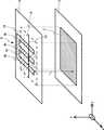
図1は、本実施形態の静電チャック100の模式図である。図2は、本実施形態の静電チャック100の要部の模式図である。 FIG. 1 is a schematic diagram of an
静電チャック100は、第1の電極2と、第2の電極4と、絶縁体50と、板60と、を有する。第2の電極4は、第1の部分4aと、第2の部分4bと、を有する。 The
第1の電極2は、第1の平面12内に設けられている。 The
第2の電極4は、第1の平面12に対し平行に設けられた第2の平面14内に設けられている。また、第2の電極4は、第2の平面14に第1の電極2が正投影された領域18と、第1の平面12及び第2の平面14に垂直な第3の平面16と、の交線20に交わる、複数の部分を有する。なお、第1の平面12、第2の平面14、第3の平面16及び交線20は、いずれも仮想的に設けられたものである。 The
ここで、X軸と、X軸に対して垂直な1つの軸であるY軸と、X軸及びY軸に対して垂直なZ軸を定義する。第1の平面12及び第2の平面14を、Z軸に垂直な平面すなわちXY平面に平行な平面とする。この場合、第3の平面16は、X軸に垂直な平面すなわちYZ平面に平行な平面である。また、交線20は、XZ平面に垂直な線すなわちY軸に平行な線である。 Here, an X axis, a Y axis which is one axis perpendicular to the X axis, and a Z axis perpendicular to the X axis and the Y axis are defined. The
例えば、第2の電極4は、第1の部分4aと、一端が第1の部分4aに電気的に接続された複数の第2の部分4bを有する。第1の部分4a及び複数の第2の部分4bは、第2の平面14内において、例えば長方形の形状を有する。複数の第2の部分4bは、それぞれが一定の距離L1を有して領域18内に配置されている。これにより、複数の第2の部分4bは、交線20に交わる。For example, the
図3は、本実施形態の他の態様の静電チャック100の要部の模式図である。第1の電極は、第1の部分2aと、第2の部分2bを有する。第2の電極は、第1の部分4a、第2の部分4b、第3の部分4c及び第4の部分4dを有する。第2の平面14に第1の部分2aが正投影された領域18aと、第2の平面14に垂直な第3の平面16aと、は1本の交線20aを形成する。また、第2の平面14に第2の部分2bが正投影された領域18bと、第2の平面14に垂直な第3の平面16bと、は1本の交線20bを形成する。そして、1本の交線20aには、複数の第2の部分4bが交わる。また、1本の交線20bには、複数の第2の部分4dが交わる。 FIG. 3 is a schematic diagram of a main part of the
なお、第2の電極4の形状は、上記のものに限定されない。 The shape of the
第1の電極2は、例えばAl(アルミニウム)の箔を用いて形成される。第2の電極4は、蒸着による形成を容易にするためMo(モリブデン)、Ni(ニッケル)、Au(金)を含むことが好ましい。ただし、第1の電極2及び第2の電極4の材料はこれに限定されない。 The
絶縁体50は、第1の電極2と第2の電極4の間に設けられている。絶縁体50は、第1の電極2と第2の電極4を適切な距離に保持する。絶縁体50は、例えばポリイミドのフィルムであるが、必ずしもこれに限定されるものではない。 The
交線20上における第2の部分4b間の距離L1は、1mm以上3mm以下、すなわち1mm≦L1≦3mmであることが好ましい。交線20上における第2の部分4bの長さL2は、0.5mm以上1mm以下、すなわち0.5mm≦L2≦1mmであることが好ましい。また、第1の電極2と第2の電極4の距離L3は、25μm以上70μm以下、すなわち25μm≦L3≦70μmであることが好ましい。DistanceL 1 between the
板60は、板60と絶縁体50の間に第2の電極4が設けられているように配置されている。板60は、半導体製造装置内において、腐食性ガス雰囲気中にプラズマが生成された環境に静電チャック100が配置される場合、静電チャックの第2の電極4や絶縁体50を腐食から保護するために用いられる。 The
板60の材質は、板60の材質の誘電率に基づいて決定されることが好ましい。例えば、窒化アルミニウム(AlN)等のセラミックスは、板60として好ましく用いられる。 The material of the
板60の膜厚は、0.6mm以上2mm以下であることが好ましい。2mmより厚い場合、第2の電極4と基板Wの距離が長くなりすぎるため、十分な大きさの静電力を基板Wに伝えて基板Wを吸着することが難しくなる。一方0.6mmより薄い場合には、薄すぎるため板60の膜厚の加工が難しくなる。 The film thickness of the
基板Wは、例えばSi(シリコン)基板等の半導体基板である。 The substrate W is a semiconductor substrate such as a Si (silicon) substrate.
基板Wは、例えば半導体基板上に、塗布等により樹脂が設けられたものであってもよい。この場合、基板Wは、板60上に、又は板60なしに第2の電極4上に、上述の樹脂が直接吸着されるように固定される。なお、基板Wが、表面に導電膜が設けられた半導体基板であり、上述の導電膜が板60上に、又は板60なしに第2の電極4上に直接吸着されるように、基板Wを固定しても良い。 The substrate W may be a substrate in which a resin is provided by coating or the like, for example. In this case, the substrate W is fixed on the
電源120は、例えば±1000V程度の電圧を印加することが可能な、市販の高電圧電源である。電源120の一方の極例えば負極は、接続配線110を用いて、第1の電極2に接続される。また、電源120の他方の極例えば正極は、接続配線110を用いて、第2の電極4に接続される。これにより、第1の電極2に負の極性を有する電圧が、また第2の電極4に正の極性を有する電圧が、それぞれ印加される。言い換えると、第1の電極2に印加される電圧の極性と、第2の電極4に印加される電圧の極性は異なっている。負極及び正極と、第1の電極2及び第2の電極4の接続は、絶縁体50内に設けられた図示しない穴等を用いて行うことができる。なお、正の極性を有する電圧が第1の電極2に、また負の極性を有する電圧が第2の電極4に印加されてもよい。 The
次に、本実施形態の静電チャック100の製造方法を記載する。まず、膜厚が4mm程度の、例えばAlNからなるセラミックス板に、Moを蒸着して第2の電極4を形成する。次に、第1の電極2となるAlの箔を、2枚のポリイミドフィルムで挟む。次に第2の電極4が形成されたセラミックス板と上述の2枚のポリイミドフィルムを、第2の電極4がポリイミドフィルムに接するように重ねて、プレス機により熱を加えながら硬化させて接着する。上述のポリイミドフィルムは絶縁体50となる。次に、板の膜厚を3mm程度削ることによりセラミックス板の膜厚を1mm程度として、板60を形成する。これにより、本実施形態の静電チャック100を得る。 Next, a method for manufacturing the
次に、本実施形態の作用効果を記載する。 Next, the effect of this embodiment is described.
図4は、本実施形態の作用効果を説明する模式図である。 FIG. 4 is a schematic diagram for explaining the function and effect of the present embodiment.
図4(a)は、本実施形態の比較形態となる静電チャック900の作用効果を説明する模式図である。静電チャック900においては、第1の電極2に負の極性を有する電圧が印加されている。これにより、第1の電極2上における基板Wの部分が正に帯電する。 FIG. 4A is a schematic diagram for explaining the operation and effect of the
また、静電チャック900においては、第2の電極4に正の極性を有する電圧が印加されている。これにより、第2の電極4上における基板Wの部分が負に帯電する。第1の電極2と基板Wの正に帯電した部分、及び第2の電極4と基板Wの負に帯電した部分に、それぞれ電気力線Eが生じ吸着力が発生する。 In the
例えば基板Wが半導体基板である場合には、基板W内部の自由電子の数が絶縁物に比較して多く、このような帯電が比較的容易に発生する。そのため、良好な吸着が可能である。しかし、基板Wが樹脂等の絶縁物で形成されている場合には、基板内部に十分な電荷がない。そのため、比較形態となる静電チャック900により絶縁物で形成された基板Wを吸着することは困難であった。 For example, when the substrate W is a semiconductor substrate, the number of free electrons in the substrate W is larger than that of an insulator, and such charging occurs relatively easily. Therefore, good adsorption is possible. However, when the substrate W is formed of an insulator such as a resin, there is not enough charge inside the substrate. Therefore, it is difficult to attract the substrate W formed of an insulator by the
また、基板Wが、半導体基板上に樹脂が設けられたものである場合には、樹脂を形成した後の基板Wの反りが大きくなるために、静電チャックへの吸着がさらに困難であるという問題があった。 In addition, when the substrate W is a semiconductor substrate provided with a resin, the warpage of the substrate W after the resin is formed becomes large, so that the adsorption to the electrostatic chuck is further difficult. There was a problem.
図4(b)は、本実施形態の静電チャック100の作用効果を説明する模式図である。本実施形態の静電チャック100においては、第1の電極2に負の極性を有する電圧が、また第2の電極4に正の極性を有する電圧が印加されている。第2の電極4から生じた電気力線Eは、基板Wに入った後静電チャック100内に戻り、第2の電極4の間を通って第1の電極2に到達する。基板W内に発生した誘電分極Pと、第2の電極4と第1の電極2の間に生じた電界強度の勾配と、の間に、グラディエント力による吸着力が発生する。 FIG. 4B is a schematic diagram for explaining the operational effects of the
静電チャック100内における第2の電極4の密度を増加させると、第2の電極4から生じて基板W内に出入りする電気力線Eの数が多くなり、より多くの誘電分極Pと電気力線Eの間に吸着力が生じるようになる。このような機構により、基板Wが、樹脂等の絶縁物で形成されている場合や、半導体基板上に樹脂が設けられたものである場合であっても、良好に静電チャック100により吸着を行うことが出来る。 When the density of the
なお、基板Wが、半導体基板や、表面に導電膜が設けられた半導体基板である場合でも、勿論良好に静電チャック100により吸着を行うことが出来る。 Even when the substrate W is a semiconductor substrate or a semiconductor substrate provided with a conductive film on the surface, it is possible to satisfactorily perform adsorption by the
L1が3mmより大きい場合、多くの第2の部分4bを領域18内に設けることが出来ないので、グラディエント力を得ることが困難になってしまう。一方、L1が1mmより小さい場合には、電荷の干渉が起こり、吸着力が弱くなる。また、この干渉により、電極が熱により破壊するおそれがある。そのため1mm≦L1≦3mmであることが好ましい。When L1 is larger than 3 mm, it is difficult to obtain a gradient force because many
L2が1mmより大きい場合、多くの第2の部分4bを領域18内に設けることが出来ないので、グラディエント力を得ることが困難になってしまう。一方、L2が0.5mmより小さい場合には、電荷の干渉が起こり、吸着力が弱くなる。また、この干渉により、電極が熱により破壊するおそれがある。そのため0.5mm≦L2≦1mmであることが好ましい。If L2 is greater than 1 mm, it is not possible to provide a number of the
L3が70μmより大きい場合、第1の電極2と第2の電極4の距離が長くなりすぎて、グラディエント力を基板Wに伝えることが出来ないため、基板Wを吸着する力が弱くなってしまう。一方、L3が25μm以下の場合、電荷の干渉が起こり、吸着力が弱くなる。また、この干渉により、電極が熱により破壊するおそれがある。そのため25μm≦L3≦70μmであることが好ましい。If L3 is greater than 70 [mu] m, the
以上のように、本実施形態の静電チャックによれば、強い吸着力を有する静電チャックの提供が可能となる。 As described above, according to the electrostatic chuck of the present embodiment, it is possible to provide an electrostatic chuck having a strong attracting force.
(第2の実施形態)
本実施形態の静電チャックは、領域内における第2の電極の端部は頂点を有する点で、第1の実施形態の静電チャックと異なっている。ここで、第1の実施形態と重複する内容については、記載を省略する。(Second Embodiment)
The electrostatic chuck of this embodiment is different from the electrostatic chuck of the first embodiment in that the end of the second electrode in the region has a vertex. Here, the description overlapping the first embodiment is omitted.
図5は、本実施形態の静電チャック100における第2の電極4の、第2の部分4bの模式図である。 FIG. 5 is a schematic view of the
図5(a)は、第2の部分4bの一部に頂点6が設けられているものである。ここで頂点6とは、2つの線の交わる点を言う。図5(a)においては、端部4cを構成する線4dと、端部4cを構成する線4eの交わる点が、頂点6となっている。このように端部4cが頂点6を有する構造とすることにより、電気力線Eの密度を増加させることが出来るため、より強い吸着力を得ることが出来る。 FIG. 5A shows a case where a
図5(b)においては、第2の部分4bが波型の形状を有する。図5(c)においては、第2の部分4bの端部4cの一部が円弧を有している。図5(b)と図5(c)の場合においても、頂点6が設けられているため、より強い吸着力を得ることが出来る。 In FIG. 5B, the
以上のように、本実施形態の静電チャックによれば、より強い吸着力を有する静電チャックの提供が可能となる。 As described above, according to the electrostatic chuck of the present embodiment, it is possible to provide an electrostatic chuck having a stronger attracting force.
(第3の実施形態)
本実施形態の静電チャックは、領域内における第2の電極は穴を有する点で、第1ないし第2の実施形態の静電チャックと異なっている。ここで、第1ないし第2の実施形態と重複する内容については、記載を省略する。(Third embodiment)
The electrostatic chuck of the present embodiment is different from the electrostatic chucks of the first and second embodiments in that the second electrode in the region has a hole. Here, the description overlapping with the first and second embodiments is omitted.
図6は、本実施形態の静電チャック100における第2の電極4の、第2の部分4bの模式図である。第2の部分4bには穴8が設けられている。この場合においても、電気力線Eの密度を増加させることが出来るため、より強い吸着力を得ることが出来る。 FIG. 6 is a schematic diagram of the
以上のように、本実施形態の静電チャックによれば、より強い吸着力を有する静電チャックの提供が可能となる。 As described above, according to the electrostatic chuck of the present embodiment, it is possible to provide an electrostatic chuck having a stronger attracting force.
(第4の実施形態)
本実施形態の半導体製造装置は、第1乃至第3の実施形態の静電チャックを備えるプラズマ処理装置である。ここで、第1乃至第3の実施形態と重複する点については、記載を省略する。(Fourth embodiment)
The semiconductor manufacturing apparatus of this embodiment is a plasma processing apparatus provided with the electrostatic chuck of the first to third embodiments. Here, the description overlapping with the first to third embodiments is omitted.
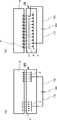
図7は、本実施形態の半導体製造装置である、プラズマ処理装置200の模式図である。ここでは、プラズマ処理装置200として、RIE(Reactive Ion Etching:反応性イオンエッチング)装置を例示している。プラズマ処理装置200は、気密に構成された、例えばアルミニウム製のチャンバ211を有している。このチャンバ211はグランド210により接地されている。 FIG. 7 is a schematic diagram of a
チャンバ211内には、基板Wを水平に支持するとともに、下部電極として機能する支持テーブル221が設けられている。支持テーブル221の表面上には、静電チャック100が設けられている。静電チャック100は、図示しない配線により、図示しない電源と接続されている。支持テーブル221の側面及び底面の周縁部を覆うように絶縁リング222が設けられている。 A support table 221 that supports the substrate W horizontally and functions as a lower electrode is provided in the
また、支持テーブル221は、チャンバ211内の中央付近に位置するように、チャンバ211に支持される図示しない支持部により固定されている。さらに、支持テーブル221には、高周波電力を供給する給電線231が接続されており、この給電線231にブロッキングコンデンサ232、整合器233及び高周波電源234が接続されている。高周波電源234からは所定の周波数の高周波電力が支持テーブル221に供給される。 Further, the support table 221 is fixed by a support portion (not shown) supported by the
下部電極として機能する支持テーブル221に対向するように、支持テーブル221の上部に上部電極242が設けられている。上部電極242は支持テーブル221と平行に対向するように、支持テーブル221から所定の距離を隔てたチャンバ211の上部付近の部品241に固定される。このような構造によって、上部電極242と支持テーブル221とは、一対の平行平板電極を構成している。また、上部電極242の内縁部には、上部電極242の板の厚さ方向を貫通する、図示しない複数のガス供給路が設けられている。上部電極242は、例えば円形状を有している。上部電極242は、例えばシリコンにより形成された電極である。 An
チャンバ211の上部付近には、プラズマ処理時に使用される処理ガスが供給されるガス供給口212が設けられており、ガス供給口212には配管を通じて図示しないガス供給装置が接続されている。 Near the upper portion of the
支持テーブル221の下部にはガス排気口213が設けられており、ガス排気口213には配管を通じて図示しない真空ポンプが接続されている。 A
チャンバ211内の支持テーブル221と、上部電極242との間の空間は、プラズマ処理室251となり、支持テーブル221と、チャンバ211の底面との間の下部の空間はガス排気室252となる。 A space between the support table 221 and the
RIE等のエッチングの際に重要なことは、エッチング中の基板Wの温度を均一にすることである。第1乃至第3の実施形態の静電チャック100を用いることにより、静電チャック100に基板Wがしっかりと吸着されるため、基板W全体の温度を静電チャック100自体の温度に制御することが容易になる。そのため、静電チャック100の温度を制御することにより、良好なエッチングを行うことが可能となる。 What is important in etching such as RIE is to make the temperature of the substrate W during etching uniform. By using the
なお、上述の記載はRIE装置についてのものであるが、第1乃至第3の実施形態の静電チャック100は、プラズマCVD(Chemical Vapor Deposition:化学気相成長)装置、スパッタ装置、MOCVD(Metal Organic Chemical Vapor Deposition:有機金属気相成長法)装置、マスク描画装置、マスク検査装置等の他の半導体製造装置にも好ましく用いることが出来る。 Although the above description is for the RIE apparatus, the
本実施形態の半導体製造装置によれば、強い吸着力を有する静電チャックを用いた半導体製造装置の提供が可能となる。 According to the semiconductor manufacturing apparatus of the present embodiment, it is possible to provide a semiconductor manufacturing apparatus using an electrostatic chuck having a strong attracting force.
(第5の実施形態)
本実施形態の半導体製造装置は、第1乃至第3の実施形態の静電チャックを備える検査装置である。ここで、第1乃至第3の実施形態と重複する点については、記載を省略する。(Fifth embodiment)
The semiconductor manufacturing apparatus according to the present embodiment is an inspection apparatus including the electrostatic chuck according to the first to third embodiments. Here, the description overlapping with the first to third embodiments is omitted.
図8は、本実施形態の半導体製造装置である、検査装置300の模式図である。 FIG. 8 is a schematic diagram of an
検査装置300は、検査ステージ310、電流端子321、電圧端子322を有する。検査ステージ310の表面には、静電チャック100が設けられている。図示しない被検査体が形成された基板Wは、静電チャック100により検査ステージ310上に固定されている。電流端子321及び電圧端子322が被検査体に接触することにより、被検査体の電気的特性の検査をすることが可能となる。 The
本実施形態の半導体製造装置によれば、強い吸着力を有する静電チャックを用いた半導体製造装置の提供が可能となる。 According to the semiconductor manufacturing apparatus of the present embodiment, it is possible to provide a semiconductor manufacturing apparatus using an electrostatic chuck having a strong attracting force.
(第6の実施形態)
本実施形態の半導体製造装置は、第1乃至第3の実施形態の静電チャックを備えるピンセットである。ここで、第1乃至第3の実施形態と重複する点については、記載を省略する。(Sixth embodiment)
The semiconductor manufacturing apparatus of this embodiment is a tweezer provided with the electrostatic chuck of the first to third embodiments. Here, the description overlapping with the first to third embodiments is omitted.
図9は、本実施形態の半導体製造装置である、ピンセット400の模式図である。ピンセット400の先端410には静電チャック100が設けられており、基板を吸着することが可能である。配線420は図示しない電源に接続されており、静電チャック100に電気を供給する。なお、持ち手430に図示しないスイッチを配置することにより、静電チャック100への電気の供給を制御してもよい。 FIG. 9 is a schematic diagram of
本実施形態の半導体製造装置によれば、強い吸着力を有する静電チャックを用いた半導体製造装置の提供が可能となる。 According to the semiconductor manufacturing apparatus of the present embodiment, it is possible to provide a semiconductor manufacturing apparatus using an electrostatic chuck having a strong attracting force.
本発明のいくつかの実施形態及び実施例を説明したが、これらの実施形態及び実施例は、例として提示したものであり、発明の範囲を限定することは意図していない。これら新規な実施形態は、その他の様々な形態で実施されることが可能であり、発明の要旨を逸脱しない範囲で、種々の省略、置き換え、変更を行うことが出来る。これら実施形態やその変形は、発明の範囲や要旨に含まれるとともに、特許請求の範囲に記載された発明とその均等の範囲に含まれる。 Although several embodiments and examples of the present invention have been described, these embodiments and examples are presented as examples and are not intended to limit the scope of the invention. These novel embodiments can be implemented in various other forms, and various omissions, replacements, and changes can be made without departing from the scope of the invention. These embodiments and modifications thereof are included in the scope and gist of the invention, and are included in the invention described in the claims and the equivalents thereof.
2 第1の電極
4 第2の電極
4a 第1の部分
4b 第2の部分
4c 端部
6 頂点
8 穴
12 第1の平面
14 第2の平面
16 第3の平面
18 領域
20 交線
50 絶縁体
60 板
100 静電チャック
110 接続配線
120 電源
200 半導体製造装置(プラズマ処理装置)
300 半導体製造装置(検査装置)
400 半導体製造装置(ピンセット)
900 静電チャック
P 誘電分極
W 基板2
300 Semiconductor manufacturing equipment (inspection equipment)
400 Semiconductor manufacturing equipment (tweezers)
900 Electrostatic chuck P Dielectric polarization W Substrate
Claims (7)
Translated fromJapanese前記第1の平面に対し平行に設けられた第2の平面内に設けられており、前記第2の平面に前記第1の電極が正投影された領域と、前記第2の平面に垂直な第3の平面と、の交線に交わる複数の部分を有する第2の電極と、
前記第1の電極と前記第2の電極の間に設けられた絶縁体と、
を備える静電チャック。A first electrode provided in a first plane;
A second plane provided in parallel with the first plane, the region on which the first electrode is orthographically projected on the second plane, and a plane perpendicular to the second plane; A second plane having a plurality of portions intersecting the intersection line with the third plane;
An insulator provided between the first electrode and the second electrode;
An electrostatic chuck comprising:
前記交線上における前記部分の長さは0.5mm以上1mm以下であり、
前記第1の電極と前記第2の電極の距離は25μm以上70μm以下である、
請求項1記載の静電チャック。The distance between the parts on the intersection line is 1 mm or more and 3 mm or less,
The length of the part on the intersection line is 0.5 mm or more and 1 mm or less,
The distance between the first electrode and the second electrode is 25 μm or more and 70 μm or less,
The electrostatic chuck according to claim 1.
請求項1又は請求項2記載の静電チャック。The polarity of the voltage applied to the first electrode is different from the polarity of the voltage applied to the second electrode.
The electrostatic chuck according to claim 1 or 2.
請求項1ないし請求項3いずれか一項記載の静電チャック。A plate is further provided, and the second electrode is provided between the plate and the insulator,
The electrostatic chuck according to claim 1.
請求項1ないし請求項4いずれか一項記載の静電チャック。An end of the second electrode in the region has a vertex;
The electrostatic chuck according to claim 1.
請求項1ないし請求項5いずれか一項記載の静電チャック。The second electrode in the region has a hole;
The electrostatic chuck according to any one of claims 1 to 5.
Priority Applications (2)
| Application Number | Priority Date | Filing Date | Title |
|---|---|---|---|
| JP2016180341AJP2018046179A (en) | 2016-09-15 | 2016-09-15 | Electrostatic chuck and semiconductor manufacturing apparatus |
| US15/449,255US10276420B2 (en) | 2016-09-15 | 2017-03-03 | Electrostatic chuck and semiconductor manufacturing apparatus |
Applications Claiming Priority (1)
| Application Number | Priority Date | Filing Date | Title |
|---|---|---|---|
| JP2016180341AJP2018046179A (en) | 2016-09-15 | 2016-09-15 | Electrostatic chuck and semiconductor manufacturing apparatus |
Publications (1)
| Publication Number | Publication Date |
|---|---|
| JP2018046179Atrue JP2018046179A (en) | 2018-03-22 |
Family
ID=61560378
Family Applications (1)
| Application Number | Title | Priority Date | Filing Date |
|---|---|---|---|
| JP2016180341AAbandonedJP2018046179A (en) | 2016-09-15 | 2016-09-15 | Electrostatic chuck and semiconductor manufacturing apparatus |
Country Status (2)
| Country | Link |
|---|---|
| US (1) | US10276420B2 (en) |
| JP (1) | JP2018046179A (en) |
Families Citing this family (23)
| Publication number | Priority date | Publication date | Assignee | Title |
|---|---|---|---|---|
| US10510575B2 (en) | 2017-09-20 | 2019-12-17 | Applied Materials, Inc. | Substrate support with multiple embedded electrodes |
| US10555412B2 (en) | 2018-05-10 | 2020-02-04 | Applied Materials, Inc. | Method of controlling ion energy distribution using a pulse generator with a current-return output stage |
| US11476145B2 (en) | 2018-11-20 | 2022-10-18 | Applied Materials, Inc. | Automatic ESC bias compensation when using pulsed DC bias |
| KR102827481B1 (en) | 2019-01-22 | 2025-06-30 | 어플라이드 머티어리얼스, 인코포레이티드 | Feedback loop to control pulse voltage waveform |
| US11508554B2 (en) | 2019-01-24 | 2022-11-22 | Applied Materials, Inc. | High voltage filter assembly |
| US11848176B2 (en) | 2020-07-31 | 2023-12-19 | Applied Materials, Inc. | Plasma processing using pulsed-voltage and radio-frequency power |
| US11798790B2 (en) | 2020-11-16 | 2023-10-24 | Applied Materials, Inc. | Apparatus and methods for controlling ion energy distribution |
| US11901157B2 (en) | 2020-11-16 | 2024-02-13 | Applied Materials, Inc. | Apparatus and methods for controlling ion energy distribution |
| US11495470B1 (en) | 2021-04-16 | 2022-11-08 | Applied Materials, Inc. | Method of enhancing etching selectivity using a pulsed plasma |
| US11791138B2 (en) | 2021-05-12 | 2023-10-17 | Applied Materials, Inc. | Automatic electrostatic chuck bias compensation during plasma processing |
| US11948780B2 (en) | 2021-05-12 | 2024-04-02 | Applied Materials, Inc. | Automatic electrostatic chuck bias compensation during plasma processing |
| US11967483B2 (en) | 2021-06-02 | 2024-04-23 | Applied Materials, Inc. | Plasma excitation with ion energy control |
| US20220399185A1 (en) | 2021-06-09 | 2022-12-15 | Applied Materials, Inc. | Plasma chamber and chamber component cleaning methods |
| US12394596B2 (en) | 2021-06-09 | 2025-08-19 | Applied Materials, Inc. | Plasma uniformity control in pulsed DC plasma chamber |
| US11810760B2 (en) | 2021-06-16 | 2023-11-07 | Applied Materials, Inc. | Apparatus and method of ion current compensation |
| US11569066B2 (en) | 2021-06-23 | 2023-01-31 | Applied Materials, Inc. | Pulsed voltage source for plasma processing applications |
| US11476090B1 (en) | 2021-08-24 | 2022-10-18 | Applied Materials, Inc. | Voltage pulse time-domain multiplexing |
| US12106938B2 (en) | 2021-09-14 | 2024-10-01 | Applied Materials, Inc. | Distortion current mitigation in a radio frequency plasma processing chamber |
| US11694876B2 (en) | 2021-12-08 | 2023-07-04 | Applied Materials, Inc. | Apparatus and method for delivering a plurality of waveform signals during plasma processing |
| US11972924B2 (en) | 2022-06-08 | 2024-04-30 | Applied Materials, Inc. | Pulsed voltage source for plasma processing applications |
| US12315732B2 (en) | 2022-06-10 | 2025-05-27 | Applied Materials, Inc. | Method and apparatus for etching a semiconductor substrate in a plasma etch chamber |
| US12272524B2 (en) | 2022-09-19 | 2025-04-08 | Applied Materials, Inc. | Wideband variable impedance load for high volume manufacturing qualification and on-site diagnostics |
| US12111341B2 (en) | 2022-10-05 | 2024-10-08 | Applied Materials, Inc. | In-situ electric field detection method and apparatus |
Family Cites Families (8)
| Publication number | Priority date | Publication date | Assignee | Title |
|---|---|---|---|---|
| JP2665242B2 (en) | 1988-09-19 | 1997-10-22 | 東陶機器株式会社 | Electrostatic chuck |
| JP2838810B2 (en) | 1990-07-16 | 1998-12-16 | 東陶機器株式会社 | Electrostatic chuck |
| US5671116A (en) | 1995-03-10 | 1997-09-23 | Lam Research Corporation | Multilayered electrostatic chuck and method of manufacture thereof |
| JP2000012194A (en) | 1998-06-29 | 2000-01-14 | Ibiden Co Ltd | Manufacture of ceramic heater |
| JP2000021961A (en) | 1998-06-29 | 2000-01-21 | Ibiden Co Ltd | Electrostatic chuck |
| US6431112B1 (en)* | 1999-06-15 | 2002-08-13 | Tokyo Electron Limited | Apparatus and method for plasma processing of a substrate utilizing an electrostatic chuck |
| WO2011000689A1 (en)* | 2009-06-30 | 2011-01-06 | Asml Holding N.V. | Image-compensating addressable electrostatic chuck system |
| JP5960384B2 (en)* | 2009-10-26 | 2016-08-02 | 新光電気工業株式会社 | Electrostatic chuck substrate and electrostatic chuck |
- 2016
- 2016-09-15JPJP2016180341Apatent/JP2018046179A/ennot_activeAbandoned
- 2017
- 2017-03-03USUS15/449,255patent/US10276420B2/ennot_activeExpired - Fee Related
Also Published As
| Publication number | Publication date |
|---|---|
| US20180076080A1 (en) | 2018-03-15 |
| US10276420B2 (en) | 2019-04-30 |
Similar Documents
| Publication | Publication Date | Title |
|---|---|---|
| JP2018046179A (en) | Electrostatic chuck and semiconductor manufacturing apparatus | |
| US11887877B2 (en) | Electrostatic chuck device | |
| TWI837214B (en) | Ground electrode formed in an electrostatic chuck for a substrate support assembly of a plasma processing chamber | |
| KR101415551B1 (en) | Electrostatic chuck, method of manufacturing the same and apparatus for processing a substrate including the same | |
| JP4951677B2 (en) | Wafer transfer device | |
| JP4935143B2 (en) | Mounting table and vacuum processing apparatus | |
| US11664261B2 (en) | Electrostatic chuck device | |
| US20190006156A1 (en) | Plasma Processing Apparatus | |
| JP2015225952A (en) | Electrostatic chuck and semiconductor/liquid crystal manufacturing device | |
| KR101134736B1 (en) | Electrostatic chuck having spacer | |
| CN113228496B (en) | Electrostatic chuck | |
| JP2013084935A (en) | Ac drive electrostatic chuck | |
| KR20150135071A (en) | Electrostatic chuck and semiconductor-liquid crystal manufacturing apparatus | |
| JP2012524417A (en) | Charge removal between substrate and electrostatic clamp | |
| TW202038019A (en) | Object table | |
| JP5351316B1 (en) | Sample holder and electron beam exposure method using the same | |
| TWI421975B (en) | Substrate mounting stand for plasma processing device, plasma processing device, and insulating coating deposition method | |
| CN108242421B (en) | Electrostatic chuck device and electrostatic adsorption method | |
| JPWO2019229784A1 (en) | Plasma processing device | |
| JP5678116B2 (en) | Lid parts, processing gas diffusion supply device, and substrate processing device | |
| KR101526509B1 (en) | Fixing chuck using lorentz force | |
| KR20190093348A (en) | Electrostatic chuck and semiconductor manufacturing device | |
| TW201933523A (en) | Electrostatic chuck and semiconductor manufacturing apparatus including a first electrode, a second electrode and an insulator | |
| US6837937B2 (en) | Plasma processing apparatus | |
| JP2004031487A (en) | Electrostatic attracting device and vacuum treating device using the same |
Legal Events
| Date | Code | Title | Description |
|---|---|---|---|
| A621 | Written request for application examination | Free format text:JAPANESE INTERMEDIATE CODE: A621 Effective date:20180828 | |
| A762 | Written abandonment of application | Free format text:JAPANESE INTERMEDIATE CODE: A762 Effective date:20190403 |