JP2018041935A - Split method - Google Patents
Split methodDownload PDFInfo
- Publication number
- JP2018041935A JP2018041935AJP2016177059AJP2016177059AJP2018041935AJP 2018041935 AJP2018041935 AJP 2018041935AJP 2016177059 AJP2016177059 AJP 2016177059AJP 2016177059 AJP2016177059 AJP 2016177059AJP 2018041935 AJP2018041935 AJP 2018041935A
- Authority
- JP
- Japan
- Prior art keywords
- protective film
- wafer
- street
- water
- solution
- Prior art date
- Legal status (The legal status is an assumption and is not a legal conclusion. Google has not performed a legal analysis and makes no representation as to the accuracy of the status listed.)
- Granted
Links
Images


Landscapes
- Laser Beam Processing (AREA)
- Dicing (AREA)
Abstract
Description
Translated fromJapanese本発明は、基板の表面側をストリートで区画した複数の領域にデバイスが形成されたウエーハを当該ストリートに沿って分割する分割方法に関する。 The present invention relates to a dividing method for dividing a wafer in which devices are formed in a plurality of regions obtained by partitioning the surface side of a substrate with a street along the street.
従来、この種のウエーハの分割方法として、ウエーハにプラズマエッチングを施してストリートに溝を形成し、ウエーハを複数のデバイスチップに分割する技術が知られている。例えば、特許文献1には、ウエーハの表面にエッチング耐性を備える水溶性保護膜を被膜し、基板のストリートに対応する部分にレーザー光を照射して基板を露出させ、露出したストリート部分にプラズマエッチングを施す分割方法が開示されている。プラズマエッチングを用いることで、ウエーハ全面にエッチング処理を一括で施すことができるため、ウエーハの大小に拘わらず処理時間を増大させないようにすることが可能となる。 Conventionally, as a method for dividing a wafer of this type, a technique is known in which plasma etching is performed on a wafer to form a groove in a street, and the wafer is divided into a plurality of device chips. For example, in Patent Document 1, a water-soluble protective film having etching resistance is coated on the surface of a wafer, the substrate is exposed by irradiating a portion corresponding to the street of the substrate with laser light, and plasma etching is performed on the exposed street portion. A dividing method for performing the above is disclosed. By using plasma etching, the entire wafer surface can be etched all at once, so that the processing time can be prevented from increasing regardless of the size of the wafer.
デバイスが形成されたウエーハでは、デバイスの設計、製造上の問題を見つけ出すために、ストリートと重なる領域に金属部材(金属パターン)を形成することがある。金属部材が形成されたウエーハにプラズマエッチングを施すためには、例えばレーザーアブレーション加工によって当該金属部材や上記特許文献1に記載のような保護膜をパターニング除去し、ストリート部分の基板を露出させる必要がある。しかしながら、ストリート上の金属部材や保護膜をアブレーションすると、除去された金属部材や基板を構成する物質の一部がデブリとなって保護膜上に堆積する。保護膜上に堆積したデブリは、ウエーハにプラズマエッチングを施す際のエッチングレートの低下の要因となるおそれがある。 In a wafer on which a device is formed, a metal member (metal pattern) may be formed in an area overlapping with a street in order to find out a problem in designing and manufacturing the device. In order to perform plasma etching on a wafer on which a metal member is formed, it is necessary to pattern-remove the metal member or the protective film described in Patent Document 1 by laser ablation, for example, to expose the substrate in the street portion. is there. However, when the metal member or the protective film on the street is ablated, a part of the removed metal member or the substance constituting the substrate becomes debris and accumulates on the protective film. The debris deposited on the protective film may cause a decrease in the etching rate when plasma etching is performed on the wafer.
本発明は、上記に鑑みてなされたものであって、ストリートと重なる領域に金属部材が形成されたウエーハにおいて、プラズマエッチングのエッチングレートの低下を抑制することができるウエーハの分割方法の提供を目的とする。 The present invention has been made in view of the above, and an object of the present invention is to provide a wafer dividing method capable of suppressing a decrease in the etching rate of plasma etching in a wafer in which a metal member is formed in an area overlapping with a street. And
上述した課題を解決し、目的を達成するために、本発明は、基板の表面側をストリートで区画した複数の領域にデバイスが形成され、該ストリートと重なる領域に金属部材が形成されたウエーハを該ストリートに沿って分割する分割方法であって、該表面に第1保護膜を形成し、該第1保護膜上に該第1保護膜とは除去特性が異なる第2保護膜を積層形成する工程と、該第1、第2保護膜が形成されたウエーハの該表面側から該ストリートに沿ってレーザー光を照射してストリート上の該第1、第2保護膜および該金属部材を除去する工程と、次いで、該ウエーハから該第2保護膜とともにウエーハにレーザー光を照射することにより該第2保護膜上に付着したデブリを除去する工程と、該第1保護膜をマスクとしてプラズマエッチングして、該ストリートに沿って溝を形成し、該ウエーハを分割する工程と、を備える。 In order to solve the above-described problems and achieve the object, the present invention provides a wafer in which a device is formed in a plurality of regions in which the surface side of a substrate is partitioned by a street, and a metal member is formed in a region overlapping the street. In this dividing method, the first protective film is formed on the surface, and a second protective film having different removal characteristics from the first protective film is formed on the first protective film. And removing the first and second protective films and the metal member on the street by irradiating laser light along the street from the surface side of the wafer on which the first and second protective films are formed. A step of removing debris adhering to the second protective film by irradiating the wafer together with the second protective film from the wafer, and plasma etching using the first protective film as a mask. The A groove is formed along the streets, and a step of dividing the wafer.
また、該第1保護膜は水溶性であり、該第2保護膜は非水溶性であることが好ましい。 The first protective film is preferably water-soluble, and the second protective film is preferably water-insoluble.
また、該第1保護膜は非水溶性であり、該第2保護膜は水溶性であることが好ましい。 The first protective film is preferably water-insoluble and the second protective film is preferably water-soluble.
本発明にかかる分割方法は、デブリの影響を受けることなくウエーハにプラズマエッチングを施すことができる。従って、本発明にかかる分割方法は、ストリートと重なる領域に金属部材が形成されたウエーハにおいて、プラズマエッチングのエッチングレートの低下を抑制することができるという効果を奏する。 The dividing method according to the present invention can perform plasma etching on a wafer without being affected by debris. Therefore, the dividing method according to the present invention has an effect that it is possible to suppress a decrease in the etching rate of plasma etching in a wafer in which a metal member is formed in a region overlapping with a street.
本発明を実施するための形態(実施形態)につき、図面を参照しつつ詳細に説明する。以下の実施形態に記載した内容により本発明が限定されるものではない。また、以下に記載した構成要素には、当業者が容易に想定できるもの、実質的に同一のものが含まれる。さらに、以下に記載した構成は適宜組み合わせることが可能である。また、本発明の要旨を逸脱しない範囲で構成の種々の省略、置換又は変更を行うことができる。 DESCRIPTION OF EMBODIMENTS Embodiments (embodiments) for carrying out the present invention will be described in detail with reference to the drawings. The present invention is not limited by the contents described in the following embodiments. The constituent elements described below include those that can be easily assumed by those skilled in the art and those that are substantially the same. Furthermore, the structures described below can be combined as appropriate. Various omissions, substitutions, or changes in the configuration can be made without departing from the scope of the present invention.
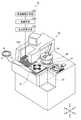
実施形態にかかるウエーハの分割方法について、図面を参照して説明する。図1は、実施形態にかかるウエーハの分割方法の加工対象であるウエーハを示す斜視図である。図2は、図1中のII−II線に沿う断面図である。 A wafer dividing method according to an embodiment will be described with reference to the drawings. FIG. 1 is a perspective view showing a wafer that is a processing target of the wafer dividing method according to the embodiment. FIG. 2 is a cross-sectional view taken along the line II-II in FIG.
実施形態にかかるウエーハの分割方法は、図1に示すウエーハWを分割する分割方法である。図1に示すウエーハWは、実施形態ではシリコン、サファイア、ガリウムヒ素などを基板Sとする円板状の半導体ウエーハや光デバイスウエーハである。ウエーハWは、図1に示すように、表面WSの交差する複数のストリート(分割予定ライン)Lによって区画された基板S上の各領域に、それぞれデバイスDが形成されている。ウエーハWは、複数のデバイスDが基板S上に形成されている。実施形態にかかるウエーハWは、ストリートLの幅が数十μm程度以下で、かつデバイスDの大きさが0.1mm以上かつ20mm以下であり、プラズマエッチングにより複数のデバイスチップDT(図15参照)に分割されるのが好適なものである。また、実施形態にかかるウエーハWの厚さは、30μm以上で且つ300μm以下である。なお、デバイスチップDTは、基板Sの一部とデバイスDとを含んで構成される。 The wafer dividing method according to the embodiment is a dividing method for dividing the wafer W shown in FIG. A wafer W shown in FIG. 1 is a disk-shaped semiconductor wafer or optical device wafer having a substrate S of silicon, sapphire, gallium arsenide, or the like in the embodiment. In the wafer W, as shown in FIG. 1, devices D are formed in each region on the substrate S defined by a plurality of streets (division planned lines) L where the surface WS intersects. In the wafer W, a plurality of devices D are formed on the substrate S. In the wafer W according to the embodiment, the width of the street L is about several tens of μm or less, the size of the device D is 0.1 mm or more and 20 mm or less, and a plurality of device chips DT are formed by plasma etching (see FIG. 15). It is preferable to be divided into two. Further, the thickness of the wafer W according to the embodiment is 30 μm or more and 300 μm or less. The device chip DT includes a part of the substrate S and the device D.
本実施形態において、デバイスDは、MOSFET(metal-oxide-semiconductor field-effect transistor)である。ウエーハWのデバイスDは、IC(Integrated Circuit)又はソースドレインなどの回路を備える。また、ウエーハWは、図2に示すように、基板SとデバイスDとの間に、絶縁膜としての機能層FLが形成されている。機能層FLを形成する絶縁膜は、SiO2膜または、SiOF、BSG(SiOB)等の無機物系の膜やポリイミド系、パリレン系等のポリマー膜である有機物系の膜からなる低誘電率絶縁体被膜(Low−k膜)からなる。なお、機能層FLは、ウエーハWから省略してもよい。また、ウエーハWは、裏面WR全面に電極となる金属膜が形成されていてもよい。In the present embodiment, the device D is a MOSFET (metal-oxide-semiconductor field-effect transistor). The device D of the wafer W includes a circuit such as an IC (Integrated Circuit) or a source / drain. In the wafer W, as shown in FIG. 2, a functional layer FL as an insulating film is formed between the substrate S and the device D. The insulating film for forming the functional layer FL is a low dielectric constant insulator made of an SiO2 film, an inorganic film such as SiOF or BSG (SiOB), or an organic film such as a polymer film such as polyimide or parylene. It consists of a coating (Low-k film). Note that the functional layer FL may be omitted from the wafer W. In addition, the wafer W may have a metal film serving as an electrode formed on the entire back surface WR.
ウエーハWのストリートLに対応する箇所は、機能層FLが除去されており、TEG(Test Element Group)等の金属部材Mが設けられている。金属部材Mは、デバイスDの設計、製造上の問題を見つけ出すための金属パターンである。金属部材Mは、プラズマエッチングにより除去が困難な導電性の金属により構成される。なお、図2に示されたウエーハWのストリートLに設けられた金属部材Mは、CMP(Chemical Mechanical Polishing)用のダミーパターンでも良い。 The functional layer FL is removed from a location corresponding to the street L of the wafer W, and a metal member M such as a TEG (Test Element Group) is provided. The metal member M is a metal pattern for finding out problems in designing and manufacturing the device D. The metal member M is made of a conductive metal that is difficult to remove by plasma etching. Note that the metal member M provided on the street L of the wafer W shown in FIG. 2 may be a dummy pattern for CMP (Chemical Mechanical Polishing).
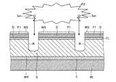
さらに、ウエーハWは、図2に示すように、デバイスD、金属部材Mおよび機能層FLの一部の表面に形成された第1保護膜F1と、第1保護膜F1上に積層して形成された第2保護膜F2とを備える。第1保護膜F1は、エッチング耐性を備えた保護膜である。本実施形態において、第1保護膜F1は、非水溶性かつ有機溶剤等の溶液(剥離液)により溶解される(剥離される)保護膜であり、例えばレジスト膜剤で形成される。第2保護膜F2は、第1保護膜F1とは除去特性が異なる保護膜である。本実施形態において、第2保護膜F2は、水溶性の保護膜であり、例えばポリビニルアルコール(polyvinyl alcohol:PVA)やポリビニルピロリドン(polyvinyl pyrrolidone:PVP)といった水溶性の樹脂材料等で形成される。すなわち、本実施形態において、第1保護膜F1と第2保護膜F2とは、第2保護膜F2を溶解させる際に使用する溶液に対する溶解特性が異なるものである。 Further, as shown in FIG. 2, the wafer W is formed by laminating the first protective film F1 formed on a part of the surface of the device D, the metal member M, and the functional layer FL, and the first protective film F1. Second protective film F2. The first protective film F1 is a protective film having etching resistance. In the present embodiment, the first protective film F1 is a water-insoluble protective film that is dissolved (peeled) by a solution (stripping solution) such as an organic solvent, and is formed of, for example, a resist film agent. The second protective film F2 is a protective film having different removal characteristics from the first protective film F1. In the present embodiment, the second protective film F2 is a water-soluble protective film, and is formed of a water-soluble resin material such as polyvinyl alcohol (PVA) or polyvinyl pyrrolidone (PVP). That is, in the present embodiment, the first protective film F1 and the second protective film F2 have different solubility characteristics with respect to the solution used when the second protective film F2 is dissolved.
次に、実施形態にかかるデバイスウエーハの分割方法について説明する。図3は、実施形態にかかるウエーハの分割方法の流れを示すフローチャートである。図4および図5は、実施形態にかかるウエーハの分割方法を実施する加工設備の構成の一例を示す模式図である。図6は、第1保護膜形成工程を実施する様子を示す断面図である。図7は、レーザー加工装置を示す説明図である。図8は、レーザー加工装置に含まれる第2保護膜形成兼除去部を示す説明図である。図9は、レーザーアブレーション工程を実施する様子を示す断面図である。図10は、レーザーアブレーション加工後のウエーハを示す断面図である。図11は、第2保護膜を除去したウエーハを示す断面図である。図12は、プラズマエッチング装置を示す説明図である。図13は、溝形成工程を実施する様子を示す断面図である。図14は、プラズマエッチング後のウエーハを示す断面図である。図15は、第1保護膜除去工程を実施する様子を示す断面図である。図16は、第1保護膜が除去されたウエーハ(デバイスチップ)を示す断面図である。 Next, a method for dividing the device wafer according to the embodiment will be described. FIG. 3 is a flowchart illustrating the flow of the wafer dividing method according to the embodiment. FIG. 4 and FIG. 5 are schematic diagrams illustrating an example of a configuration of a processing facility that performs the wafer dividing method according to the embodiment. FIG. 6 is a cross-sectional view showing a state in which the first protective film forming step is performed. FIG. 7 is an explanatory view showing a laser processing apparatus. FIG. 8 is an explanatory view showing a second protective film forming / removing part included in the laser processing apparatus. FIG. 9 is a cross-sectional view showing how the laser ablation process is performed. FIG. 10 is a cross-sectional view showing the wafer after laser ablation processing. FIG. 11 is a cross-sectional view showing the wafer from which the second protective film has been removed. FIG. 12 is an explanatory view showing a plasma etching apparatus. FIG. 13 is a cross-sectional view showing how the groove forming step is performed. FIG. 14 is a cross-sectional view showing the wafer after plasma etching. FIG. 15 is a cross-sectional view illustrating a state in which the first protective film removal step is performed. FIG. 16 is a cross-sectional view showing the wafer (device chip) from which the first protective film has been removed.
実施形態にかかるデバイスウエーハの分割方法は、図3に示すように、第1保護膜形成工程ST1と、第2保護膜形成工程ST2と、レーザーアブレーション工程ST3と、第2保護膜除去工程ST4と、溝形成工程ST5と、第1保護膜除去工程ST6とを備える。 As shown in FIG. 3, the device wafer dividing method according to the embodiment includes a first protective film forming step ST1, a second protective film forming step ST2, a laser ablation step ST3, and a second protective film removing step ST4. And a groove forming step ST5 and a first protective film removing step ST6.
本実施形態において、図3に示す各工程を実施する加工設備100は、図4に示すように、第1保護膜形成工程ST1を実施する第1保護膜形成装置10と、第2保護膜形成工程ST2、レーザーアブレーション工程ST3、および第2保護膜除去工程ST4を実施するレーザー加工装置20と、溝形成工程ST5を実施するプラズマエッチング装置40と、第1保護膜除去工程ST6を実施する第1保護膜除去装置60とを備える。また、加工設備100は、図5に示すように、第1保護膜形成装置10と、レーザー加工装置20と、プラズマエッチング装置40と、第1保護膜除去装置60の間でウエーハWを搬送するインターフェース101を備える。また、実施形態にかかるウエーハの分割方法を実施する加工設備は、ロボットを含む搬送部を中心にして各装置(各処理部)が周囲に配設されたクラスタ型のシステムであってもよい(図示せず)。 In the present embodiment, the
第1保護膜形成工程ST1は、ウエーハWのデバイスD、機能層FLの一部および金属部材Mの表面に非水溶性の第1保護膜F1を被膜する工程である。図6に示すように、第1保護膜形成工程ST1では、保護部材としてのダイシングテープTに貼着されたウエーハWの裏面WR側を第1保護膜形成装置10のスピンナテーブル11に吸着保持させ、当該スピンナテーブル11を軸心回りに回転させながら、ウエーハWに例えばレジスト膜剤といった第1保護膜溶液を第1保護膜形成装置10のノズル12から供給する。これにより、ウエーハWのデバイスD、機能層FLの一部および金属部材M上に、非水溶性かつ有機溶剤等の溶液により溶解される第1保護膜F1が被膜される。なお、本実施形態においては、環状フレームF(図7参照)に取り付けられたダイシングテープTを保護部材として用いるものとしたが、保護部材は、樹脂や硬質の材料から形成される基板であってもよい。 The first protective film forming step ST1 is a step of coating the water-insoluble first protective film F1 on the surface of the device D of the wafer W, a part of the functional layer FL, and the metal member M. As shown in FIG. 6, in the first protective film forming step ST <b> 1, the back surface WR side of the wafer W adhered to the dicing tape T as a protective member is attracted and held on the spinner table 11 of the first protective
次に、第2保護膜形成工程ST2、レーザーアブレーション工程ST3、および第2保護膜除去工程ST4を図7に示すレーザー加工装置20を用いて順次実施する。レーザー加工装置20は、図示するように、チャックテーブル21と、レーザー光照射部22と、ウエーハWを収容するカセット23と、第2保護膜形成兼除去部30とを備える。 Next, the second protective film forming step ST2, the laser ablation step ST3, and the second protective film removing step ST4 are sequentially performed using the
チャックテーブル21は、表面を構成する部分がポーラスセラミック等から形成された円板形状であり、図示しない真空吸引経路を介して図示しない真空吸引源と接続され、表面に載置されたウエーハWを吸引することで当該ウエーハWを保持する。チャックテーブル21は、X軸方向およびY軸方向に移動自在に設けられる。 The chuck table 21 has a disk shape in which a portion constituting the surface is made of porous ceramic or the like. The chuck table 21 is connected to a vacuum suction source (not shown) via a vacuum suction path (not shown), and a wafer W placed on the surface is attached to the chuck table 21. The wafer W is held by suction. The chuck table 21 is provided to be movable in the X-axis direction and the Y-axis direction.
レーザー光照射部22は、チャックテーブル21に保持されたウエーハWの表面WSにレーザーアブレーション加工を施す。レーザー光照射部22は、レーザー光を発振する発振手段22aと、レーザー光の繰り返し周波数の設定する周波数設定手段22bと、レーザー光の出力を調整する出力調整手段22cと、発振手段22aで発振されたレーザー光を集光する集光器22dとを有する。レーザー光照射部22は、チャックテーブル21に保持されたウエーハWに対して、Z軸方向に移動自在に設けられる。 The laser
カセット23は、環状フレームFに取り付けられたダイシングテープTに裏面WRが貼着されたウエーハWを複数枚収容するものである。カセット23は、図示しないカセットエレベータによりZ軸方向に移動自在に設けられる。 The
第2保護膜形成兼除去部30は、レーザーアブレーション加工前のウエーハWが第1搬送手段24により搬送されてきて、このレーザーアブレーション加工前のウエーハWに第2保護膜F2を形成するものである。また、第2保護膜形成兼除去部30は、レーザーアブレーション加工後のウエーハWが第2搬送手段25により搬送されてきて、このレーザーアブレーション加工後のウエーハWの第2保護膜F2を除去するものである。 The second protective film formation /
第2保護膜形成兼除去部30は、図8に示すように、レーザーアブレーション加工前後のウエーハWを保持するスピンナテーブル31と、スピンナテーブル31をZ軸周りに回転させる電動モータ32と、スピンナテーブル31上に保持されたウエーハWに第2保護膜F2を形成する水溶性の第2保護膜溶液を供給する保護膜溶液供給ノズル33と、スピンナテーブル31上のレーザーアブレーション加工後のウエーハWに洗浄液を供給する洗浄液供給ノズル34とを備えている。 As shown in FIG. 8, the second protective film formation /
スピンナテーブル31は、円板状に形成されて表面の中央部にポーラスセラミック等から形成された吸着チャック31aを備える。吸着チャック31aは、図示しない吸引手段に連通されている。これにより、スピンナテーブル31は、吸着チャック31aに載置されたウエーハWを吸引することでウエーハWを保持する。電動モータ32は、その駆動軸の上端にスピンナテーブル31を連結し、このスピンナテーブル31を回転自在に支持する。 The spinner table 31 includes a
保護膜溶液供給ノズル33は、第2保護膜溶液を貯留する図示しない第2保護膜溶液供給源に接続されており、水溶性の第2保護膜溶液をウエーハWに供給する。第2保護膜溶液は、例えばポリビニルアルコール(polyvinyl alcohol:PVA)やポリビニルピロリドン(polyvinyl pyrrolidone:PVP)といった水溶性の液状樹脂から構成される。また、洗浄液供給ノズル34は、第2保護膜F2を溶解させる洗浄液としての洗浄水(例えば純水)を貯留する図示しない洗浄水供給源に接続されている。 The protective film
第2保護膜形成工程ST2は、上述したレーザー加工装置20に含まれる第2保護膜形成兼除去部30によりウエーハWに第2保護膜F2を形成する工程である。ウエーハWに第2保護膜F2を形成する際には、第1保護膜形成兼除去装置10で第1保護膜F1が被膜されたウエーハWを第2保護膜形成兼除去部30のスピンナテーブル31上に搬送し、ダイシングテープTを介してスピンナテーブル31にウエーハWの裏面WR側を吸着保持させる。その後、スピンナテーブル31をZ軸回りに回転させながら、保護膜溶液供給ノズル33からウエーハWに第2保護膜溶液を供給する。これにより、図2に示すように、ウエーハWの第1保護膜F1上に第2保護膜F2が積層される。 The second protective film forming step ST2 is a step of forming the second protective film F2 on the wafer W by the second protective film forming and removing
レーザーアブレーション工程ST3は、レーザー加工装置20により、ウエーハWの表面WS側から、当該ストリートLに沿ってレーザー光を照射して、ストリートL上の第1保護膜F1、第2保護膜F2および金属部材Mを除去するレーザーアブレーション加工を施す工程である。レーザーアブレーション加工を施す際には、まず、第2保護膜形成兼除去部30のスピンナテーブル31上から第1搬送手段24によりチャックテーブル21上にウエーハWを搬送し、ダイシングテープTを介してウエーハWの裏面WR側をチャックテーブル21に吸引保持させる。その後、図9に示すように、ウエーハW(チャックテーブル21)とレーザー光照射部22の集光器22dとをストリートLに沿って相対移動させながら、当該ストリートLにレーザー光を照射する。これにより、図10に示すように、ウエーハWのストリートL上の第1保護膜F1、第2保護膜F2および金属部材Mが除去され、ストリートLの基板S表面が露出する。この際、レーザーアブレーション加工によりウエーハWから除去された金属部材Mの一部、および基板Sの一部が、デブリDEとして第2保護膜F2上に付着して堆積する。 In the laser ablation process ST3, the
第2保護膜除去工程ST4は、第2保護膜形成兼除去部30により、レーザーアブレーション加工後のウエーハWから第2保護膜F2を除去する工程である。ウエーハWから第2保護膜F2を除去する際には、レーザーアブレーション加工後のウエーハWを第2搬送手段25によって第2保護膜形成兼除去部30のスピンナテーブル31上に搬送し、ダイシングテープTを介してスピンナテーブル31にウエーハWの裏面WR側を吸着保持させる。その後、スピンナテーブル31をZ軸回りに回転させながら、洗浄液供給ノズル34からウエーハWに洗浄水を供給する。これにより、図11に示すように、第2保護膜F2が溶解されてウエーハWから除去されると共に、第2保護膜F2の除去に伴って当該第2保護膜F2上に付着して堆積したデブリDEもウエーハWから除去される。この際、第1保護膜F1は、非水溶性の保護膜であることから、洗浄水によって溶解されることなく、ウエーハWに被膜された状態を保つ。 The second protective film removing step ST4 is a step of removing the second protective film F2 from the wafer W after the laser ablation processing by the second protective film forming and removing
次に、図12に示すプラズマエッチング装置40を用いて溝形成工程ST5を実施する。溝形成工程ST5は、第1保護膜F1をマスクにして、ウエーハWの表面WS側からストリートLに沿って基板S表面の露出部分をプラズマエッチングして、ウエーハWの表面WS側から裏面WR側に延びる溝Rを形成し、ウエーハWを複数のデバイスチップDTに分割する工程である。 Next, groove forming step ST5 is performed using
溝形成工程ST5は、図12に示すプラズマエッチング装置40のハウジング41の開口42を通して、ウエーハWをハウジング41内に収容し、開口42をゲートバルブ46により閉じる。そして、ダイシングテープTを介してウエーハWの裏面WR側を高周波電源43に接続された下部電極44上の吸着保持部材45(静電チャック、ESC:Electrostatic chuck)に静電気力で吸着、保持する。 In the groove forming step ST5, the wafer W is accommodated in the
次に、図示しない冷媒供給手段から下部電極44内の図示しない冷却通路内に冷媒を循環させ、排気装置47を作動してハウジング41内の雰囲気を排気口48を通して真空排気し、ガス供給手段49から高周波電源52に接続された上部電極50の噴出口51を通してハウジング41内にエッチングガスをウエーハWの表面WS側に向けて供給する。なお、この際、ハウジング41内を所定の圧力に維持する。そして、エッチングガスを供給した状態で、高周波電源52から上部電極50に高周波電力を印加する。これにより、下部電極44と上部電極50との間にプラズマが発生し、図13に示すように、下部電極44に高周波電源43から高周波電力を供給してプラズマPZ中のイオンIonをウエーハWに引き込み、ウエーハWの表面WSをエッチングする。この際、第2保護膜除去工程ST4において、第2保護膜F2の除去に伴って、当該第2保護膜F2上に堆積したデブリDEが除去されているため、デブリDEの影響を受けることなく、ウエーハWにプラズマエッチングを施すことができる。 Next, the refrigerant is circulated from a refrigerant supply means (not shown) into a cooling passage (not shown) in the lower electrode 44, the exhaust device 47 is operated to evacuate the atmosphere in the
溝形成工程ST5において、エッチングガスの種類、高周波電源43,52が印加する高周波電力の周波数及び電力は、第1保護膜F1のエッチングレートが基板Sのエッチングレートよりも低い条件に選択される。本実施形態において、基板Sのエッチングレートの第1保護膜F1のエッチングレートに対する比(エッチング選択比)は、500以上であるとよい。例えば、高周波電源52が印加する高周波電力の周波数は、2MHz又は13.56MHzであり、高周波電源43が印加する高周波電力の周波数は、13.56MHzである。 In the groove forming step ST5, the type of etching gas and the frequency and power of the high-frequency power applied by the high-
溝形成工程ST5は、基板Sのエッチングレートが第1保護膜F1のエッチングレートよりも十分高いので、基板Sが第1保護膜F1よりも早くエッチングされ、ストリートLに表面WSから裏面WRに延びる溝Rが形成される。本実施形態においては、図14に示すように溝RがウエーハWの裏面WRに到達するまでエッチングを行った後、溝形成工程ST5を終了するが、溝形成工程ST5において形成される溝Rは、裏面WRに到達しなくても良い。即ち、本発明は、溝Rの底に基板Sの一部を残存させ、後の工程においてウエーハWを裏面WR側から研削することにより、複数のデバイスチップDTに分割するものとしてもよい。 In the groove forming step ST5, since the etching rate of the substrate S is sufficiently higher than the etching rate of the first protective film F1, the substrate S is etched faster than the first protective film F1, and extends to the street L from the front surface WS to the back surface WR. A groove R is formed. In the present embodiment, as shown in FIG. 14, the etching is performed until the groove R reaches the back surface WR of the wafer W, and then the groove forming step ST5 is finished. However, the groove R formed in the groove forming step ST5 is The rear surface WR may not be reached. That is, according to the present invention, a part of the substrate S may be left at the bottom of the groove R, and the wafer W may be ground from the back surface WR side in a later process to be divided into a plurality of device chips DT.
次に、第1保護膜除去装置60を用いて第1保護膜除去工程ST6を実施する。第1保護膜除去工程ST6は、プラズマエッチングにより溝Rが形成されて分割されたウエーハW(複数のデバイスチップDT)から第1保護膜F1を除去する工程である。ウエーハW(複数のデバイスチップDT)から第1保護膜F1を除去する際には、図15に示すように、ダイシングテープTを介してウエーハWの裏面WR側を第1保護膜除去装置60のスピンナテーブル61に吸着保持させる。その後、スピンナテーブル61を軸心回りに回転させながら、第1保護膜F1を溶解可能な有機溶剤等の溶液を第1保護膜除去装置60のノズル62からウエーハW(複数のデバイスチップDT)に供給する。これにより、図16に示すように、第1保護膜F1が溶解されてウエーハW(複数のデバイスチップDT)上から除去され、第1保護膜F1および第2保護膜F2の双方が除去された複数のデバイスチップDTを得ることができる。 Next, the first protective film removing step ST6 is performed using the first protective
以上説明したように、実施形態にかかるウエーハの分割方法は、第1保護膜F1とは除去特性(本実施形態では、第2保護膜F2を溶解させる際に使用する溶液に対する溶解特性)の異なる第2保護膜F2を当該第1保護膜F1上に積層するため、第1保護膜F1をウエーハWに被膜したまま、第2保護膜F2のみを溶解させてウエーハWから除去することができる。その結果、ストリートL上の第1保護膜F1、第2保護膜F2および金属部材Mをレーザーアブレーションによって除去した際に第2保護膜F2上に付着したデブリDEを、当該第2保護膜F2の除去に伴ってウエーハWから除去した上で、第1保護膜F1でデバイスDを保護しながら、デブリDEの影響を受けることなくウエーハWにプラズマエッチングを施すことができる。従って、実施形態にかかる分割方法は、ストリートLと重なる領域に金属部材Mが形成されたウエーハWにおいて、プラズマエッチングのエッチングレートの低下を抑制することが可能となる。 As described above, the wafer dividing method according to the embodiment is different from the first protective film F1 in the removal characteristic (in this embodiment, the dissolution characteristic with respect to the solution used when dissolving the second protective film F2). Since the second protective film F2 is laminated on the first protective film F1, only the second protective film F2 can be dissolved and removed from the wafer W while the first protective film F1 is coated on the wafer W. As a result, debris DE adhering to the second protective film F2 when the first protective film F1, the second protective film F2, and the metal member M on the street L are removed by laser ablation is removed from the second protective film F2. The wafer W can be subjected to plasma etching without being affected by the debris DE while being removed from the wafer W along with the removal, while protecting the device D with the first protective film F1. Therefore, the dividing method according to the embodiment can suppress a decrease in the etching rate of plasma etching in the wafer W in which the metal member M is formed in a region overlapping the street L.
本実施形態では、第1保護膜F1は、非水溶性の保護膜であり、第2保護膜F2は、水溶性の保護膜である。これにより、第1保護膜F1と第2保護膜F2との除去特性(本実施形態では、第2保護膜F2を溶解させる際に使用する溶液に対する溶解特性)を容易に異なるものとすることができる。その結果、第2保護膜除去工程ST4において、第1保護膜F1をウエーハWに被膜した状態を保ちつつ、第2保護膜F2をデブリDEと共にウエーハWから除去することができる。 In the present embodiment, the first protective film F1 is a water-insoluble protective film, and the second protective film F2 is a water-soluble protective film. Thereby, the removal characteristics (dissolution characteristics with respect to the solution used when dissolving the second protective film F2 in this embodiment) of the first protective film F1 and the second protective film F2 may be easily made different. it can. As a result, in the second protective film removing step ST4, the second protective film F2 can be removed from the wafer W together with the debris DE while maintaining the state where the first protective film F1 is coated on the wafer W.
ただし、第1保護膜F1および第2保護膜F2は、除去特性が異なり、第2保護膜除去工程ST4において、第1保護膜F1をウエーハWに被膜したまま、第2保護膜F2をデブリDEと共に除去可能でさえあれば、本実施形態に示したものに限られない。 However, the first protective film F1 and the second protective film F2 have different removal characteristics, and in the second protective film removal step ST4, the second protective film F2 is debris DE while the first protective film F1 is coated on the wafer W. As long as it can be removed, it is not limited to that shown in the present embodiment.
例えば、第1保護膜F1を水溶性の保護膜とし、第2保護膜F2を非水溶性かつ有機溶剤等の溶液により溶解される保護膜としてもよい。この場合、第1保護膜形成工程ST1は、第1保護膜形成装置10のノズル12から、例えばポリビニルアルコール(polyvinyl alcohol:PVA)やポリビニルピロリドン(polyvinyl pyrrolidone:PVP)といった水溶性の液状樹脂をウエーハWに供給すればよい。また、第1保護膜除去工程ST6は、第1保護膜除去装置60のノズル61から洗浄水(例えば純水)をウエーハWに供給して、第1保護膜F1を除去すればよい。第2保護膜形成工程ST2は、第2保護膜形成兼除去部30の保護膜溶液供給ノズル33から、例えばレジスト膜剤といった非水溶性の材料をウエーハWに供給し、ウエーハWの第1保護膜F1上に非水溶性の第2保護膜F2を被膜すればよい。また、第2保護膜除去工程ST4は、第2保護膜形成兼除去部30の洗浄液供給ノズル34から第2保護膜F2を溶解可能な有機溶剤等の溶液をウエーハWに供給して、デブリDEと共に第2保護膜F2を除去すればよい。 For example, the first protective film F1 may be a water-soluble protective film, and the second protective film F2 may be a water-insoluble and protective film that is dissolved by a solution such as an organic solvent. In this case, in the first protective film forming step ST1, a water-soluble liquid resin such as polyvinyl alcohol (PVA) or polyvinyl pyrrolidone (PVP) is used as a wafer from the
また、第1保護膜F1および第2保護膜F2の双方を水溶性の保護膜としてもよい。この場合、第2保護膜F2の洗浄水に対する溶解速度が第1保護膜F1の洗浄水に対する溶解速度よりも高くなるように、第1保護膜F1および第2保護膜F2を異なる水溶性の材料で形成したり、第1保護膜F1および第2保護膜F2の材料構成の比率を変更したりすれば、第2保護膜F2を溶解させる際に使用する溶液(洗浄水)に対する第1保護膜F1と第2保護膜F2との溶解特性を異なるものとすることができる。それにより、第2保護膜除去工程ST4において、第1保護膜F1をウエーハWに被膜した状態を保ちつつ、第2保護膜F2をデブリDEと共にウエーハWから除去することができる。 Further, both the first protective film F1 and the second protective film F2 may be water-soluble protective films. In this case, the first protective film F1 and the second protective film F2 are made of different water-soluble materials so that the dissolution rate of the second protective film F2 in the cleaning water is higher than the dissolution rate of the first protective film F1 in the cleaning water. The first protective film with respect to the solution (washing water) used when dissolving the second protective film F2 is formed by changing the ratio of the material structure of the first protective film F1 and the second protective film F2. The dissolution characteristics of F1 and the second protective film F2 can be made different. Thereby, in the second protective film removal step ST4, the second protective film F2 can be removed from the wafer W together with the debris DE while maintaining the state where the first protective film F1 is coated on the wafer W.
また、第1保護膜F1および第2保護膜F2の双方を非水溶性かつ有機溶剤等の溶液により溶解される保護膜としてもよい。この場合、第1保護膜F1と第2保護膜F2とを、異なる種類の溶液によって溶解する異なる材料で形成すれば、第2保護膜F2を溶解させる際に使用する溶液に対する第1保護膜F1と第2保護膜F2との溶解特性を異なるものとすることができる。また、第2保護膜F2の溶液に対する溶解速度が第1保護膜F1の溶液に対する溶解速度よりも高くなるように、第1保護膜F1および第2保護膜F2を異なる非水溶性の材料で形成したり、第1保護膜F1および第2保護膜F2の材料構成の比率を変更したりすることによっても、第2保護膜F2を溶解させる際に使用する溶液に対する第1保護膜F1と第2保護膜F2との溶解特性を異なるものとすることができる。それにより、第2保護膜除去工程ST4において、第1保護膜F1をウエーハWに被膜した状態を保ちつつ、第2保護膜F2をデブリDEと共にウエーハWから除去することができる。 Further, both the first protective film F1 and the second protective film F2 may be protective films that are water-insoluble and dissolved by a solution such as an organic solvent. In this case, if the first protective film F1 and the second protective film F2 are formed of different materials that are dissolved by different types of solutions, the first protective film F1 for the solution used when the second protective film F2 is dissolved. And the second protective film F2 can have different dissolution characteristics. Further, the first protective film F1 and the second protective film F2 are formed of different water-insoluble materials so that the dissolution rate of the second protective film F2 in the solution is higher than the dissolution rate of the first protective film F1 in the solution. Or by changing the ratio of the material configuration of the first protective film F1 and the second protective film F2, the first protective film F1 and the second protective film F2 with respect to the solution used when the second protective film F2 is dissolved. Dissolution characteristics with the protective film F2 can be made different. Thereby, in the second protective film removal step ST4, the second protective film F2 can be removed from the wafer W together with the debris DE while maintaining the state where the first protective film F1 is coated on the wafer W.
また、非水溶性の保護膜の除去手法は、有機溶剤等の溶液による溶解に限られない。例えば、酸素プラズマや窒素プラズマを用いたプラズマアッシングによって非水溶性の保護膜をウエーハWから除去してもよい。プラズマアッシングによって除去可能な非水溶性の保護膜としては、レジスト膜剤を用いるものや、ドライフィルムレジスト等が挙げられる。ドライフィルムレジストは、例えば加熱圧着によりウエーハWに被膜することができる。 Further, the removal method of the water-insoluble protective film is not limited to dissolution by a solution such as an organic solvent. For example, the water-insoluble protective film may be removed from the wafer W by plasma ashing using oxygen plasma or nitrogen plasma. Examples of the water-insoluble protective film that can be removed by plasma ashing include those using a resist film agent and dry film resists. The dry film resist can be coated on the wafer W by, for example, thermocompression bonding.
第1保護膜F1をプラズマアッシングによって除去可能な非水溶性の保護膜とした場合、例えば第2保護膜F2を水溶性の保護膜とする等、上述した手法により第2保護膜F2を溶解させる際に使用する溶液に対する第1保護膜F1と第2保護膜F2との溶解特性を異なるものとすればよい。それにより、第1保護膜F1と第2保護膜F2との除去特性を異なるものとし、第2保護膜除去工程ST4において、第1保護膜F1をウエーハWに被膜したまま、第2保護膜F2をデブリDEと共に除去することができる。また、溝形成工程ST5を実施するプラズマエッチング装置40にプラズマアッシングを実施可能なアッシングチャンバーを併設し、真空処理システム(図示せず)を構成しておけば、当該アッシングチャンバーでウエーハWにプラズマアッシングを施して第1保護膜F1を除去することができる。つまり、溝形成工程ST5および第1保護膜除去工程ST6を真空処理システム内で実施することができるため、加工工程の効率化や加工設備の簡易化を図ることができる。 When the first protective film F1 is a water-insoluble protective film that can be removed by plasma ashing, the second protective film F2 is dissolved by the above-described method, for example, the second protective film F2 is used as a water-soluble protective film. The dissolution characteristics of the first protective film F1 and the second protective film F2 with respect to the solution used at the time may be different. Thereby, the removal characteristics of the first protective film F1 and the second protective film F2 are different from each other, and the second protective film F2 remains coated on the wafer W in the second protective film removal step ST4. Can be removed together with the debris DE. In addition, if an ashing chamber capable of performing plasma ashing is provided in the
一方、第2保護膜F2をプラズマアッシングによって除去可能な非水溶性の保護膜とした場合には、第1保護膜F1は、プラズマアッシングよって除去されない保護膜でさえあればよい。それにより、第1保護膜F1と第2保護膜F2との除去特性を異なるものとし、第2保護膜除去工程ST4において、第1保護膜F1をウエーハWに被膜したまま、第2保護膜F2をデブリDEと共に除去することができる。 On the other hand, when the second protective film F2 is a water-insoluble protective film that can be removed by plasma ashing, the first protective film F1 only needs to be a protective film that is not removed by plasma ashing. Thereby, the removal characteristics of the first protective film F1 and the second protective film F2 are different from each other, and the second protective film F2 remains coated on the wafer W in the second protective film removal step ST4. Can be removed together with the debris DE.
さらに、第1保護膜F1と第2保護膜F2との除去特性を異なるものする手法は、上述したものに限られない。例えば、第1保護膜F1および第2保護膜F2の双方を同じ材料、同じ材料構成の比率で形成し、第2保護膜除去工程ST4において、第2保護膜F2がウエーハWから除去されても、第1保護膜F1が溶液によって溶解しきらず(または、プラズマアッシングにより除去されきらず)ウエーハWに残留するように、第2保護膜F2の厚みを第1保護膜F1の厚みよりも大きく形成してもよい。その結果、第2保護膜除去工程ST4において、第1保護膜F1をウエーハWに被膜した状態を保ちつつ、第2保護膜F2をデブリDEと共にウエーハWから除去することができる。 Furthermore, the method of making the removal characteristics of the first protective film F1 and the second protective film F2 different is not limited to that described above. For example, both the first protective film F1 and the second protective film F2 are formed with the same material and the same material composition ratio, and the second protective film F2 is removed from the wafer W in the second protective film removal step ST4. The thickness of the second protective film F2 is made larger than the thickness of the first protective film F1 so that the first protective film F1 is not completely dissolved by the solution (or is not completely removed by plasma ashing) and remains on the wafer W. May be. As a result, in the second protective film removing step ST4, the second protective film F2 can be removed from the wafer W together with the debris DE while maintaining the state where the first protective film F1 is coated on the wafer W.
例えば、第1保護膜F1および第2保護膜F2の一方を粘着テープとしてもよい。この場合、第1保護膜F1および第2保護膜F2の他方は、水溶性の保護膜または非水溶性の保護膜のいずれであってもよく、非水溶性の保護膜である場合は、有機溶剤等により溶解されるもの、及びプラズマアッシングにより除去されるもののいずれであってもよい。 For example, one of the first protective film F1 and the second protective film F2 may be an adhesive tape. In this case, the other of the first protective film F1 and the second protective film F2 may be either a water-soluble protective film or a water-insoluble protective film. Any of those dissolved by a solvent or the like and those removed by plasma ashing may be used.
粘着テープは、一方の面に粘着材を備えたウエーハWと同程度の径のテープ部材を用いる。第1保護膜F1を粘着テープとする場合には、第1保護膜形成工程ST1において、ウエーハWのデバイスD、機能層FLの一部および金属部材Mの表面に粘着テープの粘着材側の面を貼着する。その後、第2保護膜形成工程ST2で粘着テープ(第1保護膜F1)の粘着材と反対側の面に第2保護膜F2を形成し、レーザーアブレーション工程ST3でストリート上の粘着テープ(第1保護膜F1)、第2保護膜F2および金属部材Mを除去し、第2保護膜除去工程ST4で例えば溶液による溶解またはプラズマアッシングにより第2保護膜F2をウエーハWから除去する。これにより、粘着テープ(第1保護膜F1)をウエーハWに貼着(被膜)したまま、第2保護膜F2をデブリDEと共に除去することが可能となる。次いで、溝形成工程ST5で粘着テープ(第1保護膜F1)をマスクにして、ウエーハWにプラズマエッチングを施す。従って、第1保護膜F1を粘着テープとする場合、粘着テープは、プラズマエッチングをウエーハWに施す際にデバイスDを保護可能なエッチング耐性を備えるものを用いる。そして、第1保護膜除去工程ST6において、ウエーハW(複数のデバイスチップDT)から粘着テープ(第1保護膜F1)を剥離させる。この際、ウエーハWと同程度の径を有し、かつ、粘着テープの粘着力よりも強い粘着力を備えた剥離用テープを、ウエーハW(複数のデバイスチップDT)の全面に一旦貼着し、剥離用テープと共に各粘着テープをウエーハW(複数のデバイスチップDT)から剥がせば、粘着テープ(第1保護膜F1)を一括で除去することができる。 As the adhesive tape, a tape member having a diameter similar to that of the wafer W provided with an adhesive material on one surface is used. When the first protective film F1 is an adhesive tape, in the first protective film formation step ST1, the surface of the adhesive tape on the surface of the device D of the wafer W, a part of the functional layer FL, and the metal member M is provided. Affix. Thereafter, the second protective film F2 is formed on the surface opposite to the adhesive material of the adhesive tape (first protective film F1) in the second protective film forming step ST2, and the adhesive tape (first on the street) in the laser ablation step ST3. The protective film F1), the second protective film F2, and the metal member M are removed, and the second protective film F2 is removed from the wafer W by, for example, dissolution with a solution or plasma ashing in a second protective film removal step ST4. Accordingly, the second protective film F2 can be removed together with the debris DE while the adhesive tape (first protective film F1) is adhered (coated) to the wafer W. Next, plasma etching is performed on the wafer W using the adhesive tape (first protective film F1) as a mask in the groove forming step ST5. Therefore, when the first protective film F1 is an adhesive tape, an adhesive tape having etching resistance capable of protecting the device D when plasma etching is performed on the wafer W is used. In the first protective film removal step ST6, the adhesive tape (first protective film F1) is peeled from the wafer W (the plurality of device chips DT). At this time, a peeling tape having the same diameter as that of the wafer W and having an adhesive strength stronger than that of the adhesive tape is once stuck on the entire surface of the wafer W (multiple device chips DT). The adhesive tape (first protective film F1) can be removed in a lump by peeling each adhesive tape together with the peeling tape from the wafer W (a plurality of device chips DT).
一方、第2保護膜F2を粘着テープとする場合、第2保護膜形成工程ST2において、ウエーハWの第1保護膜F1上に粘着テープの粘着材側の面を貼着する。その後、レーザーアブレーション工程ST3でストリート上の第1保護膜F1、粘着テープ(第2保護膜F2)および金属部材Mを除去する。そして、第2保護膜除去工程ST4において、ウエーハWから粘着テープ(第2保護膜F2)のみを剥離させる。これにより、第1保護膜F1をウエーハWに被膜したまま、粘着テープ(第2保護膜F2)を、当該粘着テープ上に堆積したデブリDEと共に除去することが可能となる。なお、粘着テープ(第2保護膜F2)をウエーハWから剥離する際には、上述したように、ウエーハWと同程度の径であり、かつ、粘着テープの粘着力よりも強い粘着力を備えた剥離用テープを用いることで、粘着テープ(第2保護膜F2)を一括で除去することができる。 On the other hand, when the second protective film F2 is an adhesive tape, the adhesive tape-side surface of the adhesive tape is attached onto the first protective film F1 of the wafer W in the second protective film forming step ST2. Thereafter, the first protective film F1, the adhesive tape (second protective film F2) and the metal member M on the street are removed in the laser ablation process ST3. In the second protective film removing step ST4, only the adhesive tape (second protective film F2) is peeled off from the wafer W. As a result, the adhesive tape (second protective film F2) can be removed together with the debris DE deposited on the adhesive tape while the first protective film F1 is coated on the wafer W. When the adhesive tape (second protective film F2) is peeled off from the wafer W, as described above, it has the same diameter as the wafer W and has an adhesive strength stronger than the adhesive strength of the adhesive tape. By using the peeling tape, the adhesive tape (second protective film F2) can be removed at once.
また、実施形態にかかるウエーハの加工方法に実施する加工設備は、本実施形態に示すものに限られない。図17は、変形例にかかる加工設備100Aの構成を示す説明図である。図示するように、加工設備100Aは、加工設備100のレーザー加工装置20に代えてレーザー加工装置20A、第2保護膜形成兼除去部30に代えて、第2保護膜形成装置30Aと、第2保護膜除去装置30Bとを備える。加工設備100Aのその他の構成は、加工設備100と同様であるため、同じ符号を付し、説明を省略する。 Moreover, the processing equipment implemented in the wafer processing method according to the embodiment is not limited to that shown in the present embodiment. FIG. 17 is an explanatory diagram illustrating a configuration of a
レーザー加工装置20Aは、レーザー加工装置20から第2保護膜形成兼除去部30を省略したものである。第2保護膜形成装置30Aは、第2保護膜形成工程ST2を実施する際に用いられる。第2保護膜形成装置30Aは、例えば図6に示す第1保護膜形成装置10と同様の構成を有し、ウエーハWに第2保護膜溶液を供給可能なものである。これにより、第2保護膜形成工程ST2において、第2保護膜形成装置30AからウエーハWに第2保護膜溶液を供給し、ウエーハWの第1保護膜F1上に第2保護膜F2を積層することができる。また、第2保護膜除去装置30Bは、第2保護膜除去工程ST4を実施する際に用いられる。第2保護膜除去装置30Bは、例えば図15に示す第1保護膜除去装置60と同様の構成を有し、ウエーハWに第2保護膜F2を溶解可能な洗浄液(洗浄水、または有機溶剤等の溶液)を供給可能なものである。これにより、第2保護膜除去工程ST4において、第2保護膜除去装置30BからウエーハWに洗浄液を供給し、第2保護膜F2を溶解させて、デブリDEと共に第2保護膜F2をウエーハWから除去することができる。 The
図18は、他の変形例にかかる加工設備100Bの構成を示す説明図である。図示するように、加工設備100Bは、加工設備100のレーザー加工装置20に代えてレーザー加工装置20B、第1保護膜形成装置10および第2保護膜形成兼除去部30に代えて、保護膜形成部30Cおよび第2保護膜除去装置30Bを備える。加工設備100Bのその他の構成は、加工設備100と同様であるため、同じ符号を付し、説明を省略する。また、第2保護膜除去装置30Bは、加工設備100Aに用いられるものと同様の構成を有するため、説明を省略する。 FIG. 18 is an explanatory diagram showing a configuration of a
レーザー加工装置20Bは、図7に示すレーザー加工装置20の第2保護膜形成兼除去部30に代えて、保護膜形成部30Cを備える。保護膜形成部30Cは、第1保護膜形成工程ST1および第2保護膜形成工程ST2を実施する際に用いられる。保護膜形成部30Cは、図8に示す第2保護膜形成兼除去部30の保護膜溶液供給ノズル33に代えて、第1保護膜溶液をウエーハWに供給する第1保護膜溶液供給ノズル、洗浄液供給ノズル34に代えて、第2保護膜溶液をウエーハWに供給する第2保護膜溶液供給ノズルを備えるものである。これにより、第1保護膜形成工程ST1において、保護膜形成部30Cの第1保護膜溶液供給ノズルからウエーハWに第1保護膜溶液を供給し、ウエーハWに第1保護膜F1を形成することができる。また、第2保護膜形成工程ST2において、保護膜形成部30Cの第2保護膜溶液供給ノズルからウエーハWに第2保護膜溶液を供給し、ウエーハWの第1保護膜F1上に第2保護膜F2を積層することができる。 The
また、加工設備100、100Aにおいて、第1保護膜形成装置10と第1保護膜除去装置60とは、一体の装置であってもよい。すなわち、図8に示す第2保護膜形成兼除去部30と同様に、ウエーハWに第1保護膜溶液を供給する保護膜溶液供給ノズルと、ウエーハWに第1保護膜F1を溶解させる洗浄液(洗浄水、または有機溶剤等の溶液)を供給する洗浄液供給ノズルとを備える装置を用いて、第1保護膜形成工程ST1および第1保護膜除去工程ST6を実施してもよい。 In the
また、加工設備100Aにおいて、第2保護膜形成装置30Aと第2保護膜除去装置30Bとは、一体の装置であってもよい。すなわち、図8に示す第2保護膜形成兼除去部30をレーザー加工装置20から独立した別箇の装置とし、当該装置を用いて第2保護膜形成工程ST2および第2保護膜除去工程ST4を実施してもよい。 In the
また、加工設備100Bにおいて、第2保護膜除去装置30Bと第1保護膜除去装置60とは、一体の装置であってもよい。すなわち、ウエーハWに第1保護膜F1を溶解させる洗浄液(洗浄水、または有機溶剤等の溶液)を供給するノズルと、ウエーハWに第2保護膜F2を溶解させる洗浄液(洗浄水、または有機溶剤等の溶液)を供給するノズルとを備える装置を用いて、第2保護膜除去工程ST4および第1保護膜除去工程ST6を実施してもよい。 In the
また、加工設備100、100A、100Bにおいて、第1保護膜除去装置60は、ウエーハWから第1保護膜F1を除去可能なものであれば、本実施形態に示したものに限られず、第2保護膜除去装置30Bは、ウエーハWから第2保護膜F2を除去可能なものであれば、本実施形態に示したものに限られない。例えば、第1保護膜除去装置60または第2保護膜除去装置30Bは、上述したように、酸素プラズマや窒素プラズマを用いたプラズマアッシングにより保護膜をウエーハWから除去する装置であってもよい。また、第1保護膜除去装置60または第2保護膜除去装置30Bは、プラズマエッチング装置40に隣接して配置されてもよい。 Further, in the
また、加工設備100、100A、100Bにおいて、各装置とインターフェース101とが一つの装置に構成されてもよく、複数の装置に構成されてもよい。 Further, in the
10 第1保護膜形成装置
20,20A,20B レーザー加工装置
21 チャックテーブル
22 レーザー光照射部
22a 発振手段
22b 周波数設定手段
22c 出力調整手段
22d 集光器
23 カセット
24 第1搬送手段
25 第2搬送手段
30 第2保護膜形成兼除去部
30A 第2保護膜形成装置
30B 第2保護膜除去装置
30C 保護膜形成部
31 スピンナテーブル
31a 吸着チャック
32 電動モータ
33 保護膜溶液供給ノズル
34 洗浄液供給ノズル
40 プラズマエッチング装置
41 ハウジング
42 開口
43,52 高周波電源
44 下部電極
45 吸着保持部材
46 ゲートバルブ
47 排気装置
48 排気口
49 ガス供給手段
50 上部電極
51 噴出口
60 第1保護膜除去装置
61 スピンナテーブル
62 ノズル
100,100A,100B 加工設備
101 インターフェース
D デバイス
DT デバイスチップ
F1 第1保護膜
F2 第2保護膜
FL 機能層
Ion イオン
L ストリート(分割予定ライン)
M 金属部材
PZ プラズマ
R 溝
S 基板
W ウエーハ
WS 表面
WR 裏面DESCRIPTION OF
M Metal member PZ Plasma R Groove S Substrate W Wafer WS Front WR Back
Claims (3)
Translated fromJapanese該表面に第1保護膜を形成し、該第1保護膜上に該第1保護膜とは除去特性が異なる第2保護膜を積層形成する工程と、
該第1、第2保護膜が形成されたウエーハの該表面側から該ストリートに沿ってレーザー光を照射してストリート上の該第1、第2保護膜および該金属部材を除去する工程と、
次いで、該ウエーハから該第2保護膜とともにウエーハにレーザー光を照射することにより該第2保護膜上に付着したデブリを除去する工程と、
該第1保護膜をマスクとしてプラズマエッチングして、該ストリートに沿って溝を形成し、該ウエーハを分割する工程と、を備える分割方法。A method of dividing a wafer in which a device is formed in a plurality of regions partitioned on the surface side of the substrate by streets and a metal member is formed in a region overlapping the streets along the streets,
Forming a first protective film on the surface, and forming a second protective film on the first protective film, the second protective film having different removal characteristics from the first protective film;
Irradiating a laser beam along the street from the surface side of the wafer on which the first and second protective films are formed to remove the first and second protective films and the metal member on the street;
Next, a step of removing debris adhering to the second protective film by irradiating a laser beam to the wafer together with the second protective film from the wafer;
Dividing the wafer by plasma etching using the first protective film as a mask, forming a groove along the street, and dividing the wafer.
The dividing method according to claim 1, wherein the first protective film is water-insoluble and the second protective film is water-soluble.
Priority Applications (1)
| Application Number | Priority Date | Filing Date | Title |
|---|---|---|---|
| JP2016177059AJP6770858B2 (en) | 2016-09-09 | 2016-09-09 | Dividing method |
Applications Claiming Priority (1)
| Application Number | Priority Date | Filing Date | Title |
|---|---|---|---|
| JP2016177059AJP6770858B2 (en) | 2016-09-09 | 2016-09-09 | Dividing method |
Publications (2)
| Publication Number | Publication Date |
|---|---|
| JP2018041935Atrue JP2018041935A (en) | 2018-03-15 |
| JP6770858B2 JP6770858B2 (en) | 2020-10-21 |
Family
ID=61624080
Family Applications (1)
| Application Number | Title | Priority Date | Filing Date |
|---|---|---|---|
| JP2016177059AActiveJP6770858B2 (en) | 2016-09-09 | 2016-09-09 | Dividing method |
Country Status (1)
| Country | Link |
|---|---|
| JP (1) | JP6770858B2 (en) |
Cited By (9)
| Publication number | Priority date | Publication date | Assignee | Title |
|---|---|---|---|---|
| JP2019050237A (en)* | 2017-09-07 | 2019-03-28 | パナソニックIpマネジメント株式会社 | Manufacturing method for element chip |
| JP2019176002A (en)* | 2018-03-28 | 2019-10-10 | 株式会社ディスコ | Wafer processing method |
| JP2020027889A (en)* | 2018-08-13 | 2020-02-20 | 株式会社ディスコ | Workpiece processing method |
| JP2020035791A (en)* | 2018-08-27 | 2020-03-05 | パナソニックIpマネジメント株式会社 | Device chip manufacturing method |
| CN110911288A (en)* | 2018-09-14 | 2020-03-24 | 株式会社迪思科 | Method for machining workpiece |
| JP2020072141A (en)* | 2018-10-30 | 2020-05-07 | 株式会社ディスコ | Plasma etching apparatus and wafer processing method |
| JP2020113614A (en)* | 2019-01-10 | 2020-07-27 | 株式会社ディスコ | Wafer processing method |
| JP2020150166A (en)* | 2019-03-14 | 2020-09-17 | パナソニックIpマネジメント株式会社 | Method of manufacturing element chips |
| JP2021068778A (en)* | 2019-10-21 | 2021-04-30 | 株式会社ディスコ | Method for processing processing object |
Families Citing this family (1)
| Publication number | Priority date | Publication date | Assignee | Title |
|---|---|---|---|---|
| KR20220167106A (en) | 2021-06-11 | 2022-12-20 | 삼성전자주식회사 | Semiconductor chip, and semiconductor package |
Citations (4)
| Publication number | Priority date | Publication date | Assignee | Title |
|---|---|---|---|---|
| JP2012023085A (en)* | 2010-07-12 | 2012-02-02 | Disco Abrasive Syst Ltd | Method for processing optical device wafer |
| JP2014523109A (en)* | 2011-06-15 | 2014-09-08 | アプライド マテリアルズ インコーポレイテッド | Multilayer mask for laser substrate dicing and plasma etching |
| JP2015095508A (en)* | 2013-11-11 | 2015-05-18 | 株式会社ディスコ | Method for processing wafer |
| JP2015220240A (en)* | 2014-05-14 | 2015-12-07 | 株式会社ディスコ | Processing method for wafer |
- 2016
- 2016-09-09JPJP2016177059Apatent/JP6770858B2/enactiveActive
Patent Citations (4)
| Publication number | Priority date | Publication date | Assignee | Title |
|---|---|---|---|---|
| JP2012023085A (en)* | 2010-07-12 | 2012-02-02 | Disco Abrasive Syst Ltd | Method for processing optical device wafer |
| JP2014523109A (en)* | 2011-06-15 | 2014-09-08 | アプライド マテリアルズ インコーポレイテッド | Multilayer mask for laser substrate dicing and plasma etching |
| JP2015095508A (en)* | 2013-11-11 | 2015-05-18 | 株式会社ディスコ | Method for processing wafer |
| JP2015220240A (en)* | 2014-05-14 | 2015-12-07 | 株式会社ディスコ | Processing method for wafer |
Cited By (16)
| Publication number | Priority date | Publication date | Assignee | Title |
|---|---|---|---|---|
| JP2019050237A (en)* | 2017-09-07 | 2019-03-28 | パナソニックIpマネジメント株式会社 | Manufacturing method for element chip |
| JP7042437B2 (en) | 2017-09-07 | 2022-03-28 | パナソニックIpマネジメント株式会社 | Method of manufacturing element chips |
| JP7037412B2 (en) | 2018-03-28 | 2022-03-16 | 株式会社ディスコ | Wafer processing method |
| JP2019176002A (en)* | 2018-03-28 | 2019-10-10 | 株式会社ディスコ | Wafer processing method |
| JP2020027889A (en)* | 2018-08-13 | 2020-02-20 | 株式会社ディスコ | Workpiece processing method |
| JP7154697B2 (en) | 2018-08-13 | 2022-10-18 | 株式会社ディスコ | Workpiece processing method |
| JP2020035791A (en)* | 2018-08-27 | 2020-03-05 | パナソニックIpマネジメント株式会社 | Device chip manufacturing method |
| JP7149517B2 (en) | 2018-08-27 | 2022-10-07 | パナソニックIpマネジメント株式会社 | Element chip manufacturing method |
| CN110911288A (en)* | 2018-09-14 | 2020-03-24 | 株式会社迪思科 | Method for machining workpiece |
| TWI827670B (en)* | 2018-09-14 | 2024-01-01 | 日商迪思科股份有限公司 | Workpiece processing method |
| CN110911288B (en)* | 2018-09-14 | 2024-02-23 | 株式会社迪思科 | Method for machining workpiece |
| JP2020072141A (en)* | 2018-10-30 | 2020-05-07 | 株式会社ディスコ | Plasma etching apparatus and wafer processing method |
| JP2020113614A (en)* | 2019-01-10 | 2020-07-27 | 株式会社ディスコ | Wafer processing method |
| JP2020150166A (en)* | 2019-03-14 | 2020-09-17 | パナソニックIpマネジメント株式会社 | Method of manufacturing element chips |
| JP7357237B2 (en) | 2019-03-14 | 2023-10-06 | パナソニックIpマネジメント株式会社 | Manufacturing method of element chip |
| JP2021068778A (en)* | 2019-10-21 | 2021-04-30 | 株式会社ディスコ | Method for processing processing object |
Also Published As
| Publication number | Publication date |
|---|---|
| JP6770858B2 (en) | 2020-10-21 |
Similar Documents
| Publication | Publication Date | Title |
|---|---|---|
| JP6770858B2 (en) | Dividing method | |
| CN106847747B (en) | Method for dividing wafer | |
| JP6509744B2 (en) | Laser plasma etching wafer dicing with etching chamber shield ring for film frame wafer application | |
| US9379015B2 (en) | Wafer processing method | |
| JP6519759B2 (en) | Method of manufacturing element chip | |
| JP6560969B2 (en) | Wafer division method | |
| TWI698954B (en) | Dicing wafers having solder bumps on wafer backside | |
| US10083867B2 (en) | Method of processing a wafer | |
| JPWO2003071591A1 (en) | Method for dividing semiconductor wafer | |
| CN111312658B (en) | Wafer processing method | |
| KR20130130834A (en) | Method and system for wafer level singulation | |
| JP2019079884A (en) | Wafer processing method | |
| JP2018046208A (en) | Wafer processing method | |
| US11024542B2 (en) | Manufacturing method of device chip | |
| US20220093464A1 (en) | Device chip manufacturing method | |
| CN109473352B (en) | Manufacturing method of component chip | |
| JP2019212769A (en) | Wafer processing method | |
| JP7061022B2 (en) | Wafer processing method | |
| JP7083716B2 (en) | Wafer processing method | |
| JP7207969B2 (en) | Wafer processing method | |
| JP6689154B2 (en) | Device wafer processing method | |
| JP2024157478A (en) | Processing method | |
| JP2023091896A (en) | Device chip manufacturing method | |
| KR20230050240A (en) | Method for manufacturing device chip | |
| CN117334640A (en) | Method for processing device wafer |
Legal Events
| Date | Code | Title | Description |
|---|---|---|---|
| A621 | Written request for application examination | Free format text:JAPANESE INTERMEDIATE CODE: A621 Effective date:20190725 | |
| A977 | Report on retrieval | Free format text:JAPANESE INTERMEDIATE CODE: A971007 Effective date:20200520 | |
| A131 | Notification of reasons for refusal | Free format text:JAPANESE INTERMEDIATE CODE: A131 Effective date:20200623 | |
| A521 | Request for written amendment filed | Free format text:JAPANESE INTERMEDIATE CODE: A523 Effective date:20200807 | |
| TRDD | Decision of grant or rejection written | ||
| A01 | Written decision to grant a patent or to grant a registration (utility model) | Free format text:JAPANESE INTERMEDIATE CODE: A01 Effective date:20200908 | |
| A61 | First payment of annual fees (during grant procedure) | Free format text:JAPANESE INTERMEDIATE CODE: A61 Effective date:20200928 | |
| R150 | Certificate of patent or registration of utility model | Ref document number:6770858 Country of ref document:JP Free format text:JAPANESE INTERMEDIATE CODE: R150 | |
| R250 | Receipt of annual fees | Free format text:JAPANESE INTERMEDIATE CODE: R250 | |
| R250 | Receipt of annual fees | Free format text:JAPANESE INTERMEDIATE CODE: R250 |