JP2017535902A - Optical device and reading device - Google Patents
Optical device and reading deviceDownload PDFInfo
- Publication number
- JP2017535902A JP2017535902AJP2017545010AJP2017545010AJP2017535902AJP 2017535902 AJP2017535902 AJP 2017535902AJP 2017545010 AJP2017545010 AJP 2017545010AJP 2017545010 AJP2017545010 AJP 2017545010AJP 2017535902 AJP2017535902 AJP 2017535902A
- Authority
- JP
- Japan
- Prior art keywords
- light
- unit
- card
- medium
- imaging
- Prior art date
- Legal status (The legal status is an assumption and is not a legal conclusion. Google has not performed a legal analysis and makes no representation as to the accuracy of the status listed.)
- Pending
Links
Images


Classifications
- G—PHYSICS
- G06—COMPUTING OR CALCULATING; COUNTING
- G06F—ELECTRIC DIGITAL DATA PROCESSING
- G06F3/00—Input arrangements for transferring data to be processed into a form capable of being handled by the computer; Output arrangements for transferring data from processing unit to output unit, e.g. interface arrangements
- G06F3/01—Input arrangements or combined input and output arrangements for interaction between user and computer
- G06F3/03—Arrangements for converting the position or the displacement of a member into a coded form
- G06F3/041—Digitisers, e.g. for touch screens or touch pads, characterised by the transducing means
- G06F3/0412—Digitisers structurally integrated in a display
- G—PHYSICS
- G06—COMPUTING OR CALCULATING; COUNTING
- G06F—ELECTRIC DIGITAL DATA PROCESSING
- G06F3/00—Input arrangements for transferring data to be processed into a form capable of being handled by the computer; Output arrangements for transferring data from processing unit to output unit, e.g. interface arrangements
- G06F3/01—Input arrangements or combined input and output arrangements for interaction between user and computer
- G06F3/03—Arrangements for converting the position or the displacement of a member into a coded form
- G06F3/041—Digitisers, e.g. for touch screens or touch pads, characterised by the transducing means
- G06F3/042—Digitisers, e.g. for touch screens or touch pads, characterised by the transducing means by opto-electronic means
- G06F3/0425—Digitisers, e.g. for touch screens or touch pads, characterised by the transducing means by opto-electronic means using a single imaging device like a video camera for tracking the absolute position of a single or a plurality of objects with respect to an imaged reference surface, e.g. video camera imaging a display or a projection screen, a table or a wall surface, on which a computer generated image is displayed or projected
- G—PHYSICS
- G06—COMPUTING OR CALCULATING; COUNTING
- G06V—IMAGE OR VIDEO RECOGNITION OR UNDERSTANDING
- G06V10/00—Arrangements for image or video recognition or understanding
- G06V10/10—Image acquisition
- G06V10/12—Details of acquisition arrangements; Constructional details thereof
- G06V10/14—Optical characteristics of the device performing the acquisition or on the illumination arrangements
- G06V10/141—Control of illumination
- G—PHYSICS
- G06—COMPUTING OR CALCULATING; COUNTING
- G06V—IMAGE OR VIDEO RECOGNITION OR UNDERSTANDING
- G06V10/00—Arrangements for image or video recognition or understanding
- G06V10/10—Image acquisition
- G06V10/12—Details of acquisition arrangements; Constructional details thereof
- G06V10/14—Optical characteristics of the device performing the acquisition or on the illumination arrangements
- G06V10/145—Illumination specially adapted for pattern recognition, e.g. using gratings
- G—PHYSICS
- G06—COMPUTING OR CALCULATING; COUNTING
- G06V—IMAGE OR VIDEO RECOGNITION OR UNDERSTANDING
- G06V30/00—Character recognition; Recognising digital ink; Document-oriented image-based pattern recognition
- G06V30/10—Character recognition
- G06V30/22—Character recognition characterised by the type of writing
- G06V30/224—Character recognition characterised by the type of writing of printed characters having additional code marks or containing code marks
- G—PHYSICS
- G07—CHECKING-DEVICES
- G07F—COIN-FREED OR LIKE APPARATUS
- G07F17/00—Coin-freed apparatus for hiring articles; Coin-freed facilities or services
- G07F17/32—Coin-freed apparatus for hiring articles; Coin-freed facilities or services for games, toys, sports, or amusements
- G07F17/3202—Hardware aspects of a gaming system, e.g. components, construction, architecture thereof
- G07F17/3216—Construction aspects of a gaming system, e.g. housing, seats, ergonomic aspects
- G07F17/322—Casino tables, e.g. tables having integrated screens, chip detection means
- G—PHYSICS
- G07—CHECKING-DEVICES
- G07F—COIN-FREED OR LIKE APPARATUS
- G07F17/00—Coin-freed apparatus for hiring articles; Coin-freed facilities or services
- G07F17/32—Coin-freed apparatus for hiring articles; Coin-freed facilities or services for games, toys, sports, or amusements
- G07F17/3286—Type of games
- G07F17/3293—Card games, e.g. poker, canasta, black jack
- G—PHYSICS
- G06—COMPUTING OR CALCULATING; COUNTING
- G06V—IMAGE OR VIDEO RECOGNITION OR UNDERSTANDING
- G06V10/00—Arrangements for image or video recognition or understanding
- G06V10/10—Image acquisition
- G06V10/12—Details of acquisition arrangements; Constructional details thereof
- G06V10/14—Optical characteristics of the device performing the acquisition or on the illumination arrangements
- G06V10/143—Sensing or illuminating at different wavelengths
- G—PHYSICS
- G06—COMPUTING OR CALCULATING; COUNTING
- G06V—IMAGE OR VIDEO RECOGNITION OR UNDERSTANDING
- G06V10/00—Arrangements for image or video recognition or understanding
- G06V10/10—Image acquisition
- G06V10/16—Image acquisition using multiple overlapping images; Image stitching
Landscapes
- Engineering & Computer Science (AREA)
- Theoretical Computer Science (AREA)
- Physics & Mathematics (AREA)
- General Physics & Mathematics (AREA)
- General Engineering & Computer Science (AREA)
- Multimedia (AREA)
- Computer Vision & Pattern Recognition (AREA)
- Human Computer Interaction (AREA)
- Artificial Intelligence (AREA)
- Image Input (AREA)
Abstract
Translated fromJapaneseDescription
Translated fromJapanese本発明は、光学装置及び読取装置に関する。 The present invention relates to an optical device and a reading device.
従来、ゲームセンタ等に設置されるアーケードゲーム機や、家庭用のテレビモニタ等に接続して用いるゲーム機において、カードをゲーム機のステージ上に載置してプレイするカードゲーム装置が知られている(特許文献1参照)。
また、プレイヤにより載置されたカードの数値やゲーム結果等、ゲームに関する情報を、プロジェクタを用いてステージ上に映像で表示するゲーム装置も提案されている(特許文献2参照)。Conventionally, in an arcade game machine installed in a game center or the like, or a game machine used by connecting to a home TV monitor or the like, a card game apparatus is known that plays by placing a card on the stage of the game machine. (See Patent Document 1).
There has also been proposed a game apparatus that displays information about a game such as a numerical value of a card placed by a player and a game result on a stage using a projector (see Patent Document 2).
しかしながら、特許文献1のゲーム機では、ゲーム機筐体内に設けられたカメラは1個のみであり、解像度の制限から、カードを載置するステージ面を大きくすると、カードの向きや座標、異なるコード等、種々の情報を精密に読み取れないという問題があった。さらに、解像度を高くした場合、カメラのコストアップだけでなく、高解像度のためカードを認識するための超高速のCPU(Central Processing Unit)と大容量のRAM(Read Only Memory:記憶媒体)も必要となり大幅なコストアップとなる。さらにまた、ステージ面のサイズに合わせたシステムを毎回、開発する必要がある。
また、特許文献2のゲーム機では、カード等を載置するステージが設けられたゲーム機筐体に支柱を設け、支柱の上にプロジェクタ等の表示装置を設置するため、大掛かりな装置となり、ゲームセンタ等に設置しづらいという問題がある。However, in the game machine of
Further, in the game machine of
そこで、本発明者らは、ステージ面に載置された媒体の情報を確実かつ効率的に読み取ることができるとともに、演出効果及びセキュリティの高い情報出力装置を発明し、特許出願をしている(特許文献3参照)。 Therefore, the present inventors have invented an information output device that can reliably and efficiently read information on a medium placed on the stage surface, and has a high effect and security, and has applied for a patent ( (See Patent Document 3).
しかしながら、ステージ面のサイズを大きくする等、ステージ面のサイズの柔軟性が要求されているところ、特許文献3の技術では当該要求に応えることは困難である。さらに、ステージ面を照射するLED(Light Emitting Diode) がステージ面周辺の下部近傍に配置されており、ステージ面のサイズを大きくした場合、光を均一に照射するには難があった。 However, the flexibility of the size of the stage surface, such as increasing the size of the stage surface, is required. However, it is difficult to meet this requirement with the technology of
本発明は、このような状況に鑑みてなされたものであり、任意のサイズのステージ面を有するボードゲームやテーブルトップディスプレイを容易に実現可能にすることを目的とする。 The present invention has been made in view of such a situation, and an object thereof is to easily realize a board game or a table top display having a stage surface of an arbitrary size.
上記目的を達成するため、本発明の一態様の光学装置は、
裏面側から照射された光のうち少なくとも一部の第1光を表面に通過させると共に、所定の媒体を前記表面側に配置可能な平面板と、
前記平面板の裏面側から前記光を照射する発光部と、
前記平面板を介して、前記媒体で反射された前記第1光で露光することで、前記媒体を撮像する撮像部と、
前記発光部から照射された光のうち前記平面板にて反射された第2光の、前記撮像部への入射を禁止するように、前記発光部から照射された光の照射方向を規制する規制部と、
を備える。In order to achieve the above object, an optical device of one embodiment of the present invention includes:
A flat plate that allows at least a portion of the first light of the light irradiated from the back side to pass through the surface, and can arrange a predetermined medium on the surface side;
A light emitting unit for irradiating the light from the back side of the flat plate;
An imaging unit that images the medium by exposing with the first light reflected by the medium through the plane plate;
Regulation that regulates the irradiation direction of the light emitted from the light emitting unit so that the second light reflected by the flat plate out of the light emitted from the light emitting unit is prohibited from entering the imaging unit. And
Is provided.
前記撮像部により撮像された前記媒体の特徴、又は当該媒体に付された情報を認識する認識部
をさらに備えることができる。The information processing apparatus may further include a recognition unit that recognizes characteristics of the medium imaged by the imaging unit or information attached to the medium.
前記認識部は、前記媒体の特徴として、前記媒体の形状と大きさのうち少なくとも一方を認識する
ことができる。The recognizing unit can recognize at least one of a shape and a size of the medium as a characteristic of the medium.
前記媒体には、画像、文字、図形、若しくは記号又はこれらの結合が形成されており、
前記認識部は、前記画像、前記文字、前記図形、前記記号又は前記これらの結合を認識する
ことができる。In the medium, an image, a character, a figure, or a symbol or a combination thereof is formed,
The recognition unit can recognize the image, the character, the graphic, the symbol, or the combination thereof.
前記媒体は、第1光の反射率が他と異なる部分を少なくとも一部に含んでおり、
前記認識部は、前記第1光の反射率が他と異なる部分を認識する
ことができる。The medium includes at least part of a portion where the reflectance of the first light is different from the others,
The recognition unit can recognize a portion where the reflectance of the first light is different from the others.
前記媒体には、第1光の反射率が他と異なる部分として、前記画像、前記文字、前記図形、若しくは前記記号又は前記これらの結合が形成されている
ことができる。In the medium, the image, the character, the graphic, the symbol, or the combination thereof may be formed as a portion where the reflectance of the first light is different from others.
前記媒体の前記第1光の反射率が他と異なる部分は、前記第1光を反射させるドットであり、
前記第1光を非反射させる前記媒体の面に、複数の前記ドットからなるドットパターンが形成されており、
前記認識部は、前記ドットパターンを認識する
ことができる。A portion where the reflectance of the first light of the medium is different from others is a dot that reflects the first light,
A dot pattern composed of a plurality of the dots is formed on a surface of the medium that does not reflect the first light;
The recognition unit can recognize the dot pattern.
前記媒体の前記第1光の反射率が他と異なる部分は、前記第1光を非反射させるドットであり、
前記第1光を反射させる前記媒体の面に、複数の前記ドットからなるドットパターンが形成されており、
前記認識部は、前記ドットパターンを認識する
ことができる。The portion where the reflectance of the first light of the medium is different from the others is a dot that makes the first light non-reflective,
A dot pattern composed of a plurality of the dots is formed on the surface of the medium that reflects the first light,
The recognition unit can recognize the dot pattern.
前記撮像部を複数個備え、
前記平面板において、複数の前記撮像部の夫々により撮像される各撮像領域は、少なくとも1つの他の前記撮像部により撮像される撮像領域と重複する重複領域を有している、
ことができる。A plurality of the imaging units are provided,
In the plane plate, each imaging region imaged by each of the plurality of imaging units has an overlapping region that overlaps an imaging region imaged by at least one other imaging unit,
be able to.
前記発光部を複数個備え、
前記平面板は、複数の前記発光部により照射され、
前記規制部は、さらに、当該規制部が無い場合と比較して、前記平面板における光量差を抑制すると共に、光量差がある領域では光量の変化の度合を抑制するように、前記複数の発光部のうち少なくとも一部から照射された光の照射方向を規制する、
ことができる。A plurality of the light emitting units are provided,
The flat plate is irradiated by a plurality of the light emitting units,
The restricting portion further suppresses the light amount difference in the flat plate as compared with the case where the restricting portion is not provided, and the plurality of light emission so as to suppress the degree of change in the light amount in an area where the light amount difference exists. Regulating the irradiation direction of the light emitted from at least a part of the part,
be able to.
前記撮像部の撮像領域を照射する前記発光部の発光中に、当該撮像部を露光させる制御部をさらに備える、
ことができる。A control unit that exposes the imaging unit during light emission of the light emitting unit that irradiates the imaging region of the imaging unit;
be able to.
前記撮像部による露光期間内の所定時間だけ、当該撮像部の撮像領域を照射する前記発光部から光を照射させる制御を実行する制御部をさらに備える、
ことができる。A control unit that executes control to irradiate light from the light emitting unit that irradiates the imaging region of the imaging unit for a predetermined time within an exposure period by the imaging unit;
be able to.
前記複数の撮像部で撮像された画像のうち、前記媒体の少なくとも一部を被写体として含む画像を1以上用いて、前記平面板を基準とする座標系で前記媒体の位置を認識する認識部、
をさらに備えることができる。A recognition unit for recognizing the position of the medium in a coordinate system based on the plane plate using one or more images including at least a part of the medium as a subject among images captured by the plurality of imaging units;
Can further be provided.
前記平面板は、透過スクリーンの機能を有し、
前記透過スクリーンに可視光で画像を投影可能なプロジェクタ
をさらに備えることができる。The flat plate has a function of a transmission screen,
The projector may further include a projector capable of projecting an image with visible light on the transmission screen.
前記発光部から照射される光は非可視光である、
ことができる。The light emitted from the light emitting unit is invisible light,
be able to.
前記発光部から照射される光は、白色の可視光であり、
所定時間だけ前記発光部から光を照射させる制御を実行する制御部と、
前記撮像部により撮像された画像を用いて、前記平面板に配置された前記媒体を認識する認識部と、
をさらに備えることができる。The light emitted from the light emitting unit is white visible light,
A control unit that executes control to emit light from the light emitting unit for a predetermined time; and
A recognition unit for recognizing the medium arranged on the flat plate using an image captured by the imaging unit;
Can further be provided.
前記制御部は、さらに、前記撮像部において光電変換された画像信号を保持するバッファをクリアした後、前記撮像部の露光タイミングと前記発光部の照射タイミングとを同期させる制御を実行する、
ことができる。The control unit further executes control to synchronize the exposure timing of the imaging unit and the irradiation timing of the light emitting unit after clearing a buffer that holds an image signal photoelectrically converted in the imaging unit.
be able to.
本発明によれば、任意のサイズのステージ面を有するボードゲームを容易に実現可能にすることができる。 According to the present invention, a board game having a stage surface of an arbitrary size can be easily realized.
以下、図面を参照しながら、本発明の実施形態について説明する。 Hereinafter, embodiments of the present invention will be described with reference to the drawings.
[光学装置の概要]
図1は、本発明の一実施形態に係る光学装置10の外観的構成の一例を示す斜視図である。
図1に示す光学装置10は、プレイヤが所有するカードC1,C2等(以下、これらをまとめて「カードC」と呼ぶ)を載置するためのカード配置パネル11と、当該カード配置パネル11を搭載する台座部12とを備えている。
つまり、プレイヤにとっては、光学装置10は、カードCを用いた所定のボードゲームをプレイするためのテーブルであり、カード配置パネル11は、ステージ面として機能する。
なお、プレイヤからみて、カード配置パネル11は、台座部12の上に載せられている。そこで、以下、台座部12側を「下側」とし、カード配置パネル11側を「上側」として説明をする。
また、実際には、台座部12は筐体(図示せず)により覆われて内部は視認できないが、図1の例では筐体の図示が省略されている。[Outline of optical device]
FIG. 1 is a perspective view showing an example of an external configuration of an
An
That is, for the player, the
From the viewpoint of the player, the
Actually, the
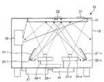
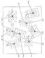
図2は、図1の光学装置10の内部構造の概略を示す断面図である。
図2に示すように、光学装置10は、その台座部12の筐体内部に、n個(nは2以上の任意の整数値)の規制部21−1乃至21−nと、短焦点プロジェクタ22と、n個の撮像部23−1乃至23−nと、n個のユニット制御部24−1乃至24−nと、n個の発光部25−1乃至25−nとを備える。
また、光学装置10は、その台座部12の筐体の下側に、パネル全体制御部26と、主制御部27とを備える。FIG. 2 is a cross-sectional view schematically showing the internal structure of the
As shown in FIG. 2, the
In addition, the
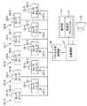
図3は、図1の光学装置10のうち、電気信号を処理する構成要素を示すブロック図である。 FIG. 3 is a block diagram showing components that process electrical signals in the
本実施形態では、撮像部23−k(kは、1乃至nの任意の整数値である)とユニット制御部24−kとの組が、1ユニットで取り扱われる。そこで、以下、このようなユニットを、センサユニット30−kと呼ぶ。
つまり、図3の例では、n=10のセンサユニット30−1乃至30−nが設けられている。これらセンサユニット30−1乃至30−nは、図2に示すように、例えば台座部12の筐体下部に配置される。In this embodiment, a set of the imaging unit 23-k (k is an arbitrary integer value from 1 to n) and the unit control unit 24-k is handled by one unit. Therefore, hereinafter, such a unit is referred to as a sensor unit 30-k.
That is, in the example of FIG. 3, n = 10 sensor units 30-1 to 30-n are provided. As shown in FIG. 2, these sensor units 30-1 to 30-n are arranged, for example, at the lower part of the casing of the
センサユニット30−1乃至30−nの夫々は、例えば、ケーブルで接続されており、ケーブルは図示せぬHuBユニット等を介してパネル全体制御部26に接続されている。
センサユニット30−1乃至30−nの接続方法は、1つの輪で繋がれるチェーン接続でもよく、複数の輪で接続されてもよい。接続の方法は全く任意であり、無線接続であってもよい。センサ毎のブロック化はできなくなるが1つの基板上に複数のセンサを配置してもよい。パネル全体制御部26は、主制御部27に接続されている。主制御部27には、表示部31とスピーカ32とが接続されている。
表示部31は、本実施形態では少なくとも短焦点プロジェクタ22を含んでおり、その他図示せぬディスプレイを含めるようにしてもよい。Each of the sensor units 30-1 to 30-n is connected by, for example, a cable, and the cable is connected to the overall
The connection method of the sensor units 30-1 to 30-n may be a chain connection connected by one ring or may be connected by a plurality of rings. The connection method is completely arbitrary, and may be a wireless connection. Although it becomes impossible to block each sensor, a plurality of sensors may be arranged on one substrate. The panel
The
なお、以下、センサユニット30−1乃至30−nの各々を区別する必要がない場合、それらをまとめて、「センサユニット30」と呼ぶ。また、センサユニット30と呼ぶ場合、規制部21−1乃至21−nもまとめて「規制部21」と呼び、撮像部23−1乃至23−nもまとめて「撮像部23」と呼び、ユニット制御部24−1乃至24−nもまとめて「ユニット制御部24」と呼び、かつ「発光部25−1乃至25−n」もまとめて「発光部25」と呼ぶ。 Hereinafter, when it is not necessary to distinguish each of the sensor units 30-1 to 30-n, they are collectively referred to as a “sensor unit 30”. When the sensor unit 30 is referred to, the restriction units 21-1 to 21-n are collectively referred to as “
センサユニット30において、撮像部23は、レンズと、CMOS又はCCD型の撮像素子とを含むように構成されている。
撮像部23のセンサの下部には、ユニット制御部24が配置される。ユニット制御部24は、CPUとフレームバッファとを含むように構成されている。メモリーを省力化するため、フレームバッファはラインバッファに変更してもよい。その際は、所定のスキャンライン方式による二値化処理を実施することになる。
撮像部23のセンサにより取り込まれた画像のデータは、ユニット制御部24のCPUにより画像処理が施される。In the sensor unit 30, the
A
The image data captured by the sensor of the
ここで、本実施形態では、レンズの上面には、IRフィルタが貼付されているものとする。このIRフィルタは、少なくとも発光部25で発光される赤外線波長(700nm以上)の赤外光LOを透過させる光学特性を有するフィルタである。
つまり、本実施形態では、図4に示す発光部25−1を含む全ての発光部25は、赤外光LOを発光する。
カード配置パネル11は、裏面側から照射された赤外光LOのうち少なくとも一部の第1光LSを表面に通過させる。
ここで、カードCの少なくとも一部が赤外線を拡散反射させる領域(以下、「赤外線反射領域」と呼ぶ)を含む場合、カードCの赤外線反射領域から拡散反射された赤外光は、レンズ及びIRフィルタを介して撮像部23のセンサに入射される。撮像部23のセンサは、当該赤外光で露光することで、カードCの赤外線反射領域が写る画像を撮像する。
例えば図4の例では、カード配置パネル11のうち、撮像部23−10の撮像領域P2内にカードCが配置されている。従って、撮像部23−10により撮像された画像に、カードCの赤外線反射領域が写ることになる。Here, in this embodiment, an IR filter is attached to the upper surface of the lens. This IR filter is a filter having optical characteristics that transmits at least infrared light LO having an infrared wavelength (700 nm or more) emitted from the
That is, in this embodiment, all the
The
Here, when at least a part of the card C includes a region that diffuses and reflects infrared rays (hereinafter referred to as “infrared reflection region”), the infrared light diffusely reflected from the infrared reflection region of the card C is transmitted to the lens and the IR. The light enters the sensor of the
For example, in the example of FIG. 4, the card C is arranged in the imaging area P <b> 2 of the imaging unit 23-10 in the
図4に図示はしないが同様に、カード配置パネル11のうち、撮像部23−1の撮像領域P1内にカードCが配置されていた場合、当該撮像部23−1により撮像された画像に、カードCの赤外線反射領域が写ることになる。
この場合、撮像部23−1のセンサに入射される赤外光は、撮像部23−10側に配置された発光部25−10(図4には図示せぬ)から発光されて、カードCの赤外線反射領域にて拡散反射されたものである。
ここで、カード配置パネル11は、ガラス、アクリル、その他の平滑な裏面を有する板状の媒体である。
このため、図4に示すように、発光部25−1から発光された赤外光LOは、全てカード配置パネル11の盤面を透過して透過光LSとなるわけではなく、その一部がカード配置パネル11の盤面で鏡面反射して反射光LRとなる。
この発光部25−1からの反射光LRが仮に、当該発光部25−1の反対側に配置された撮像部23−10のセンサ(撮像領域P1を撮像する各画素群)に入射されてしまうと、撮像部23−10により撮像される画像に、外乱光として写り込んでしまう。この外乱光のため、カードCの赤外線反射領域が認識困難となるおそれがある。
そこで、本実施形態では、発光部25−1から照射された赤外光LOのうちカード配置パネル11にて鏡面反射された反射光LRの、撮像部23−10のセンサへの入射を禁止するように、発光部25−1から照射された赤外光LOの照射方向を規制する規制部21−1が設けられている。
なお、反射光LRは、規制部21−1により、発光部25−1から離間した撮像部23−10のセンサへの入射が禁止されているので、その結果として当然ながら、発光部25−1の近傍の撮像部23−1のセンサへの入射も禁止される。
ここで、カードCの位置等の解析(認識)は、実際には、撮像領域P1内で定義される所定の領域(以下、「解析領域」と呼ぶ)において行われる。したがって、より正確には、反射光LRは、仮に撮像部23−10のセンサに入射されたとしても、解析領域を撮像する各画素群に入射されなければ、カードCの赤外線反射領域の認識は可能になる。つまり、規制部21−1は、撮像部23−10のセンサを構成する各画素群のうち、解析領域を撮像する各画素群への反射光LOの入射を禁止するように、発光部25−1から照射された赤外光LOの照射方向を規制すればよい。
このように、撮像領域と解析領域とは、独立した概念の別々の領域であるが、説明の便宜上、本実施形態では撮像領域と解析領域とは一致しているものとする。
同様に、発光部25−2乃至25−10の夫々についても、カード配置パネル11の盤面にて鏡面反射された反射光LRの、撮像部23のセンサへの入射を禁止するように、発光部25−2乃至25−10の夫々から照射された光の照射方向を規制する規制部21−2乃至21−10が設けられている。
これら規制部21−1乃至21−nは、図2に示すように、例えば台座部12の筐体下部に配置される。Similarly, although not shown in FIG. 4, when the card C is arranged in the imaging region P <b> 1 of the imaging unit 23-1 in the
In this case, infrared light incident on the sensor of the imaging unit 23-1 is emitted from a light emitting unit 25-10 (not shown in FIG. 4) disposed on the imaging unit 23-10 side, and the card C The light is diffusely reflected in the infrared reflection region.
Here, the
For this reason, as shown in FIG. 4, the infrared light LO emitted from the light emitting unit 25-1 does not all pass through the board surface of the
The reflected light LR from the light emitting unit 25-1 is incident on the sensor (each pixel group that images the imaging region P1) of the imaging unit 23-10 disposed on the opposite side of the light emitting unit 25-1. Then, it will be reflected as disturbance light in the image picked up by the image pickup unit 23-10. This disturbance light may make it difficult to recognize the infrared reflection area of the card C.
Accordingly, in the present embodiment, the reflected light LR that is specularly reflected by the
The reflected light LR is prohibited from entering the sensor of the imaging unit 23-10 separated from the light emitting unit 25-1 by the regulating unit 21-1, and as a result, of course, the light emitting unit 25-1 Incident to the sensor of the imaging unit 23-1 in the vicinity of is also prohibited.
Here, the analysis (recognition) of the position or the like of the card C is actually performed in a predetermined area (hereinafter referred to as “analysis area”) defined in the imaging area P1. Therefore, more precisely, even if the reflected light LR is incident on the sensor of the imaging unit 23-10, if the reflected light LR is not incident on each pixel group that images the analysis area, the infrared reflection area of the card C is recognized. It becomes possible. That is, the restricting unit 21-1 emits the reflected light LO to each pixel group that configures the sensor of the imaging unit 23-10 and prohibits the reflected light LO from entering each pixel group that images the analysis region. The irradiation direction of the infrared light LO irradiated from 1 may be regulated.
As described above, the imaging region and the analysis region are separate regions having independent concepts. However, for convenience of explanation, it is assumed that the imaging region and the analysis region coincide with each other in this embodiment.
Similarly, for each of the light emitting units 25-2 to 25-10, the light emitting unit 25-2 is also configured to prohibit the reflected light LR specularly reflected by the board surface of the
As shown in FIG. 2, these restricting portions 21-1 to 21-n are disposed, for example, at the lower portion of the casing of the
ここで、図4に示すように、カードC(赤外線反射領域)の全てが、撮像部23−10の解析領域(撮像領域P2)の中に含まれている場合には、当該撮像部23−10の撮像画像だけで、カードC(赤外線反射領域)全体の認識は可能である。
しかしながら、カードC(赤外線反射領域)の一部のみが、撮像部23−10の解析領域(撮像領域P2)の中に含まれている場合には、当該撮像部23−10の撮像画像だけで、カードC(赤外線反射領域)全体の認識をすることは非常に困難である。
つまり、この場合、カードC(赤外線反射領域)の残りの一部は、1以上の他の撮像部23の解析領域(図4の例では撮像部23−1の撮像領域P1)の中に含まれていることになる。
この場合、原則として、複数の撮像部23の撮像画像を合成することにより、カードC(赤外線反射領域)全体の認識が可能になる。しかしながら、解析領域を重複させない場合、カードCの重要部分(例えば後述するドットパターンの1単位等)がちょうど境界の境目に配置されてしまうと、当該重要部分の認識エラーが発生してしまうおそれもある。
そこで、本実施形態では、カード配置パネル11において、撮像部23の夫々により撮像される各解析領域は、少なくとも1つの他の撮像部23により撮像される解析領域と重複する重複領域を有している。
図4の例では、撮像部23−1の解析領域としての撮像領域P1と、撮像部23−2の解析領域としての撮像領域P2とが重複する重複領域が設けられている。Here, as shown in FIG. 4, when all of the card C (infrared reflection area) is included in the analysis area (imaging area P2) of the imaging unit 23-10, the imaging unit 23- The entire card C (infrared reflection area) can be recognized with only 10 captured images.
However, when only a part of the card C (infrared reflection area) is included in the analysis area (imaging area P2) of the imaging unit 23-10, only the captured image of the imaging unit 23-10 is used. It is very difficult to recognize the entire card C (infrared reflective area).
That is, in this case, the remaining part of the card C (infrared reflective area) is included in one or more other analysis areas of the imaging unit 23 (in the example of FIG. 4, the imaging area P1 of the imaging unit 23-1). Will be.
In this case, in principle, it is possible to recognize the entire card C (infrared reflection area) by combining the captured images of the plurality of
Therefore, in the present embodiment, in the
In the example of FIG. 4, an overlapping region is provided in which the imaging region P1 as the analysis region of the imaging unit 23-1 and the imaging region P2 as the analysis region of the imaging unit 23-2 overlap.
図5は、10個の撮像部23−1乃至23−10の各解析領域の夫々が重複領域を有しつつ配置されて構成される、カードCの位置等を解析するための全体の解析領域の一例を示している。
全体の解析領域は、カード配置パネル11上に定義され、図5に示すように、所定の座標系(左上端がX=0,Y=0となり、右下端がX=1999,Y=1065となる座標系)が定義される。このような座標系を、以下、「カード解析全体座標系」と呼ぶ。なお、X=0,Y=0の原点は、どの隅に配置してもよいことは言うまでもない。
全体の解析領域は、10個の撮像部23−1乃至23−10の各解析領域(図5の点線で示される各撮像領域P1乃至P10)の夫々が重複領域を有しつつ配置されて構成される。
全体の解析領域のサイズは、横W×縦Hとなる。FIG. 5 shows an entire analysis area for analyzing the position and the like of the card C, in which each analysis area of the ten imaging units 23-1 to 23-10 is arranged with an overlapping area. An example is shown.
The entire analysis area is defined on the
The entire analysis region is configured by arranging each analysis region (each image pickup region P1 to P10 indicated by a dotted line in FIG. 5) of the ten image pickup units 23-1 to 23-10 while having an overlap region. Is done.
The size of the entire analysis region is W × H.
図5の例では、10個の撮像部23−1乃至23−10が、2行×5列の形態で縦横等間隔に配置されている。具体的には、縦方向については、全体の解析領域の長辺からh1だけ離れた位置であって、縦方向に隣接する2つの撮像部23の間隔(例えば撮像部23−1と撮像部23−10との間隔は)がh2となるように、10個の撮像部23−1乃至23−10は配置される。また、横方向については、全体の解析領域の短辺からw1だけ離れた位置であって、横方向に隣接する2つの撮像部23の間隔(例えば撮像部23−1と撮像部23−2との間隔は)がw2となるように、10個の撮像部23−1乃至23−10は配置される。
換言すると、10個の撮像部23−1乃至23−10が上述のように夫々配置されると、図5に示す全体の解析領域が形成される。In the example of FIG. 5, ten image pickup units 23-1 to 23-10 are arranged at equal intervals in the form of 2 rows × 5 columns. Specifically, with respect to the vertical direction, the distance between the two
In other words, when the ten imaging units 23-1 to 23-10 are arranged as described above, the entire analysis region shown in FIG. 5 is formed.
本実施形態では、1つの撮像部23の撮像領域が、対応するユニット制御部24によりカードCの位置等が解析される解析領域となる。そこで以下、このような1つのユニット制御部24による解析領域を、全体の解析領域と区別すべく、「サブ解析領域」と呼ぶ。サブ解析領域(撮像部23の撮像領域)のサイズは、横Dw×縦Dhとなる。 In the present embodiment, the imaging region of one
重複領域は、縦方向に隣接する2つのサブ解析領域が重複することで形成される領域(以下、「縦重複領域」と呼ぶ)と、横方向に隣接する2つのサブ解析領域が重複することで形成される領域(以下、「横重複領域」と呼ぶ)とがある。
縦重複領域の縦方向のサイズは、縦Dh0である。つまり、解析領域の2つの長辺から夫々Dh1だけ離れた位置に縦重複領域が形成される。
横重複領域の横方向のサイズは、横Dmoである。つまり、解析領域の2つの短辺に一番近い横重複領域については、当該2つの短辺から夫々Dm1だけ離れた位置に横重複領域が形成される。2つの横重複領域の間の間隔は、横Dmoになる。
なお、図5に示すように、このような縦重複領域と横重複領域とがさらに重複する領域も存在する。The overlapping area is an area formed by overlapping two sub-analysis areas adjacent in the vertical direction (hereinafter referred to as “vertical overlapping area”), and two sub-analysis areas adjacent in the horizontal direction overlap. (Hereinafter referred to as “horizontal overlap region”).
The vertical size of the vertical overlap region is vertical Dh0. That is, a vertical overlap region is formed at a position separated from the two long sides of the analysis region by Dh1.
The horizontal size of the horizontal overlap region is horizontal Dmo. In other words, for the horizontal overlap region closest to the two short sides of the analysis region, the horizontal overlap region is formed at a position separated from the two short sides by Dm1. The interval between the two horizontal overlap areas is horizontal Dmo.
Note that, as shown in FIG. 5, there is a region where such a vertical overlap region and a horizontal overlap region further overlap.
即ち、サブ解析領域(撮像領域)P1乃至P10の夫々においては、ローカル座標系が定義される。この場合、カードCが配置されたサブ解析領域について、対応するユニット制御部24により当該カードCの座標等がローカル座標系で算出される。
ここで、カードCが重複領域に配置されている場合には、当該重複領域を形成する複数のサブ解析領域毎に、夫々のローカル座標系でカードCの座標値が算出される。
そして、後述するパネル全体制御部26により、カードCの座標値が「カード解析全体座標系」に変換される。
このようにして、後段の主制御部27にとっては、あたかも1個の光学モジュールでカードCの位置等が解析されたのと等価な解析結果が通知されるので、カード配置パネル11全体におけるカードCの位置(カード解析全体座標系での座標値)を容易に認識することが可能になる。That is, a local coordinate system is defined in each of the sub analysis areas (imaging areas) P1 to P10. In this case, for the sub-analysis region in which the card C is arranged, the corresponding
Here, when the card C is arranged in the overlapping area, the coordinate value of the card C is calculated in each local coordinate system for each of the plurality of sub-analysis areas forming the overlapping area.
And the coordinate value of the card | curd C is converted into the "card analysis whole coordinate system" by the panel
In this way, the subsequent
即ち、カード配置パネル11のサイズが(センサユニット30から相対的にみて)小さければ、1つのセンサユニット30のみでカードCの位置等を解析することができる。
しかしながら、本実施形態のカード配置パネル11のサイズは大きく、当該カード配置パネル11上を任意に移動し得るカードCについて、その位置等を解析するためには、1つのセンサユニット30では足らない。
そこで、複数個のセンサユニット30を組合せることで、あたかも1個の光学モジュール(センサユニット30)で解析したのと等価な解析を行えるようにしている。That is, if the size of the
However, the size of the
Therefore, by combining a plurality of sensor units 30, an analysis equivalent to that performed by a single optical module (sensor unit 30) can be performed.
同様に、カード配置パネル11のサイズが(発光部25から相対的にみて)小さければ、1つの発光部25のみで、当該カード配置パネル11全体をムラなく(照射光量に差が無いように)赤外光を照射することができる。
しかしながら、本実施形態のカード配置パネル11のサイズは大きいため、1つの発光部25のみで、当該カード配置パネル11全体をムラなく(照射光量に差が無いように)赤外光を照射することは非常に困難である。
そこで、本実施形態では複数の発光部25が設けられている。
ただし、単に複数の発光部25を設けただけでは、上述したように、カード配置パネル11での反射光の写り込みが問題となるため、カード配置パネル11での反射光の撮像部23への入射を禁止すべく、規制部21が設けられている。Similarly, if the size of the
However, since the size of the
Therefore, in the present embodiment, a plurality of light emitting
However, simply providing a plurality of light emitting
ここで、規制部21として、発光部25からの発光を一律に規制するものを採用した場合、当該カード配置パネル11においてムラが出る領域、即ち、照射量が他とは異なる領域が生じてしまい、その領域の内外における照射量の変化の度合も大きくなるという問題が生じる。つまり、かかる領域にカードCが配置された場合、カードCの認識の解析に悪影響を及ぼすという問題が生じる。
そこで、この問題を解決すべく、本実施形態の規制部21は、図6に示す形状を有している。Here, when the
Therefore, in order to solve this problem, the restricting
図6は、本実施形態の規制部21の外観構成を示す図である。
図6(a)は、規制部21の遮光面側を示す図である。
図6(b)は、規制部21の筐体への取付面側を示す図である。
図6(c)は、規制部21の断面図を示す図である。FIG. 6 is a diagram illustrating an external configuration of the
FIG. 6A is a diagram showing the light shielding surface side of the restricting
FIG. 6B is a diagram showing the attachment surface side of the restricting
FIG. 6C is a diagram showing a cross-sectional view of the restricting
図6(a)及び(c)に示すように、規制部21は、完全遮光部21aと、一部遮光部21bとに大別される。
つまり、図6(a)及び(c)の左端側であって、図6(a)に示す遮光面の反対側(図6(c)では下側)に、発光部25が配置される。
従って、発光部25から発光された赤外光は、完全遮光部21aにおいては完全に遮光される一方、一部遮光部21bにおいては完全には遮光されず一部が漏れ光として外部に照射される。
この一部遮光部21bは、いわゆるのこぎり刃状の形状を有しており、遮光面の面積が先端(図6(a)及び(c)の右端)にいくほど小さくなっている。つまり、先端にいくほど漏れ光の光量が徐々に多くなる。As shown in FIGS. 6A and 6C, the restricting
That is, the
Accordingly, the infrared light emitted from the
The partial light-shielding
ここで、図7を参照して、規制部21に一部遮光部21bを設けた意義について説明する。
図7は、規制部21に一部遮光部21bを設けた意義を説明する図である。Here, with reference to FIG. 7, the significance of providing the
FIG. 7 is a diagram for explaining the significance of providing a partial
図7(a)は、規制部21に一部遮光部21bを設けない場合における、カード配置パネル11における照射量の分布を示している。
即ち、図7(a)において、上側の図は、カード配置パネル11における照射量の位置変化を示す図であり、下側の図は、対となる発光部25−1,25−10のカード配置パネル11に対する照射の状況を説明する模式図である。FIG. 7A shows the distribution of the irradiation amount on the
That is, in FIG. 7A, the upper diagram is a diagram showing the position change of the irradiation amount on the
図7(a)に示すように、発光部25−1から照射された赤外光L1は、規制部21−1により規制されて、カード配置パネル11のうち位置c乃至dの範囲に照射される。この場合、赤外光L1による照射量(光量)は、位置a乃至cの範囲では光量0となり、位置c乃至dの範囲では一定光量Rとなる。 As shown in FIG. 7A, the infrared light L <b> 1 emitted from the light emitting unit 25-1 is regulated by the regulating unit 21-1 and is radiated to the range of positions c to d on the
また、発光部25−10から照射された赤外光L10は、規制部21−10により規制されて、カード配置パネル11のうち位置a乃至bの範囲に照射される。この場合、赤外光L10による照射量(光量)は、位置a乃至bの範囲では一定光量Rとなり、位置b乃至dの範囲では光量0となる。 Further, the infrared light L10 emitted from the light emitting unit 25-10 is regulated by the regulating unit 21-10, and is radiated to the range of positions a to b in the
即ち、カード配置パネル11全体の照射量(光量)としては、赤外光L1による照射量(光量)と赤外光L10による照射量(光量)との和になるので、図7(a)の一番上のチャートに示すように、位置a乃至bの範囲と位置c乃至dの範囲では一定光量Rであるところ、位置b乃至cの範囲では光量0となり、光量の差ができている。さらに、その光量の変化の度合も急である。 That is, the irradiation amount (light amount) of the entire
図7(b)は、本実施形態のように規制部21に一部遮光部21bを設けた場合における、カード配置パネル11における照射量の分布を示している。
なお、図7(b)における上側の図と下側の図の関係は、図7(a)の関係と同一であるため、ここではその説明は省略する。ここで、図示しないが、図6の21のような減光領域を規制部21を設けない場合は、位置b乃至cの範囲では光量が2×Rとなり、均一な光量とはならず、かかる領域にカードCが配置された場合、カードCを認識の解析に悪影響を及ぼすという問題が生じる。FIG. 7B shows the irradiation amount distribution in the
Note that the relationship between the upper diagram and the lower diagram in FIG. 7B is the same as the relationship in FIG. 7A, so the description thereof is omitted here. Here, although not shown, when the light reduction region as shown in 21 of FIG. 6 is not provided with the restricting
図7(b)に示すように、発光部25−1から照射された赤外光L1は、規制部21−1により規制されるが、一部遮光部21−1bにおいては全て遮光されずに漏れ光が生じ、当該漏れ光が、カード配置パネル11のうち位置b乃至cに照射される。
しかも一部遮光部21−1bの漏れ量(即ち照射量)は、図6を用いて上述したように、先端に行くほど(位置bから位置cに近づくほど)大きくなっていく。つまり、赤外光L1による照射量(光量)は、位置a乃至cの範囲では光量0となり、位置b乃至cの範囲では徐々に上昇して一定光量Rに近づき、位置c乃至dの範囲では一定光量Rとなる。As shown in FIG. 7B, the infrared light L1 emitted from the light emitting unit 25-1 is regulated by the regulating unit 21-1, but is not completely shielded by the partial light shielding unit 21-1b. Leakage light is generated, and the leak light is applied to the positions b to c of the
In addition, as described above with reference to FIG. 6, the leakage amount (that is, the irradiation amount) of the partial light-shielding portion 21-1 b increases as it approaches the tip (as it approaches the position c from the position b). That is, the irradiation amount (light quantity) by the infrared light L1 becomes 0 in the range of positions a to c, gradually increases in the range of positions b to c, approaches a constant light quantity R, and in the range of positions c to d. The amount of light R is constant.
発光部25−10から照射された赤外光L10は、規制部21−10により規制されるが、一部遮光部21−10bにおいては全て遮光されずに漏れ光が生じ、当該漏れ光が、カード配置パネル11のうち位置b乃至cに照射される。
しかも一部遮光部21−10bの漏れ量(即ち照射量)は、図6を用いて上述したように、先端に行くほど(位置cから位置bに近づくほど)大きくなっていく。つまり、赤外光L10による照射量(光量)は、位置a乃至bの範囲では一定光量Rとなり、位置b乃至cの範囲では徐々に下降して光量0に近づき、位置c乃至dの範囲では光量0となる。The infrared light L10 emitted from the light emitting unit 25-10 is regulated by the regulating unit 21-10. However, in some of the light shielding units 21-10b, leakage light is generated without being blocked, and the leakage light is The positions b to c of the
In addition, as described above with reference to FIG. 6, the leakage amount (that is, the irradiation amount) of the partial light-shielding portion 21-10 b increases as it approaches the tip (closer to the position b from the position c). That is, the irradiation amount (light quantity) by the infrared light L10 becomes a constant light quantity R in the range of the positions a to b, gradually decreases in the range of the positions b to c, approaches 0, and in the range of the positions c to d. The amount of light is zero.
即ち、カード配置パネル11全体の照射量(光量)としては、赤外光L1による照射量(光量)と赤外光L10による照射量(光量)との和になるので、図7(b)の一番上のチャートに示すように、位置a乃至dの全範囲において一定光量Rになる。 That is, the irradiation amount (light amount) of the entire
もっとも、図7(b)の一番上のチャートは理想的なものであり、実施には、位置b乃至cの範囲の照射量は、一部遮光部21−1bの漏れ量と一部遮光部21−10bの漏れ量との加算量であるため、一定光量Rを維持するのは困難な点もある。
しかしながら、一部遮光部21bを設けない図7(a)との比較の観点では、一部遮光部21bを用いることで、カード配置パネル11における光量差を抑制すると共に、光量差がある領域(即ち位置b乃至cの範囲)では光量の変化の度合を抑制することが実現可能になっている。However, the top chart in FIG. 7B is ideal, and in practice, the amount of irradiation in the range of positions b to c is the amount of leakage from the partial light shielding portion 21-1b and the partial light shielding. Since it is an addition amount with the leakage amount of the part 21-10b, it is difficult to maintain the constant light amount R.
However, from the viewpoint of comparison with FIG. 7A in which the partial light-shielding
換言すると、一部遮光部21bを有する規制部21としては、当該規制部21が無い場合(一部遮光部21bを有しない完全遮光部21aのみからなる規制部21)と比較して、カード配置パネル11における光量差を抑制すると共に、光量差がある領域では光量の変化の度合を抑制するように、複数の発光部25のうち少なくとも一部から照射された光の照射方向を規制すれば足りる。
即ち、一部遮光部21bの形状等は、図6の例に特に限定されず、カード配置パネル11における光量差を抑制すると共に、光量差がある領域では光量の変化の度合を抑制することが可能な形状等であれば任意のものを採用することができる。例えば、乳白色のアクリル製で透過光を徐々に変化させるようにアクリル板の厚さを変化させたり、透明度が変化するような材料を使用してもよい。In other words, as the restricting
That is, the shape or the like of the partial light-shielding
以上まとめると、カード配置パネル11は、図4に示すように、裏面側から照射された赤外光のうち少なくとも一部の第1光LSを表面に通過させると共に、図1に示すように、カードCを表面側に配置可能な平面板である。
例えば図4に示すように、発光部25−1は、カード配置パネル11の裏面側から赤外光を照射する。
撮像部23−10は、カード配置パネル11を介して、カードC(より正確には赤外線反射領域)で反射された第1光LSで露光することで、カードCを撮像する。
ユニット制御部24−10は、撮像領域P2をサブ解析領域として、カードCの位置等をローカル座標系で解析する。
ここで、図4を例としたため、撮像領域P2をサブ解析領域として担当する撮像部23−10及びユニット制御部24−10、即ちセンサユニット30−10の解析処理として説明したが、当該解析処理は、カードCの少なくとも一部が配置されたサブ解析領域を担当するセンサユニット30においても実行される。
図3のパネル全体制御部26は、これらのセンサユニット30の各解析処理を統合することで、カード配置パネル11に配置された1枚以上のカードC(図1の例では2枚のカードC1,C2)の位置等を、カード解析全体座標系で認識する。
主制御部27は、1枚以上のカードCの認識結果を用いて、ボードゲーム全体に関する制御を実行し、その実行結果を画像として表示部31に表示したり、音声としてスピーカ32から出力する。In summary, as shown in FIG. 4, the
For example, as shown in FIG. 4, the light emitting unit 25-1 irradiates infrared light from the back side of the
The imaging unit 23-10 images the card C by exposing with the first light LS reflected by the card C (more precisely, the infrared reflection region) via the
The unit controller 24-10 analyzes the position and the like of the card C in the local coordinate system with the imaging area P2 as a sub-analysis area.
Here, since FIG. 4 was taken as an example, the analysis processing of the imaging unit 23-10 and the unit control unit 24-10 that are in charge of the imaging region P2 as a sub-analysis region, that is, the sensor unit 30-10 has been described. Is also executed in the sensor unit 30 in charge of the sub-analysis region in which at least a part of the card C is arranged.
The panel
The
ここで、本実施形態では、任意の数のセンサユニット30を適用することができるので、カード配置パネル11のサイズは特に限定されず、例えばこれまでにない大きなサイズを採用することも容易にできる。 Here, in this embodiment, since an arbitrary number of sensor units 30 can be applied, the size of the
ただし、複数のセンサユニット30を適用する場合には、各種各様な措置が必要になる。 However, when applying a plurality of sensor units 30, various measures are required.
例えば図4に示すように、発光部25−1から照射された赤外光のうちカード配置パネル11にて反射された第2光LSが、撮像部23−1に入射されると、当該第2光LSが外乱光として写り込んでしまう。この場合、カードCの認識処理に悪影響を及ぼすことになる。
そこで、本実施形態では、発光部25−1から照射された赤外光のうちカード配置パネル11にて反射された第2光LSの、撮像部23−1への入射を禁止するように、発光部25−1から照射された赤外光の照射方向を規制する規制部21−1が備えられている。
同様の趣旨で規制部21−1乃至21−10も備えられている。For example, as illustrated in FIG. 4, when the second light LS reflected by the
Therefore, in the present embodiment, the second light LS reflected by the
For the same purpose, restricting units 21-1 to 21-10 are also provided.
さらに、本実施形態の規制部21は、当該規制部21(一部遮光部21b)が無い場合と比較して、カード配置パネル11における光量差を抑制すると共に、光量差がある領域では光量の変化の度合を抑制するように(図7参照)、複数の発光部25のうち少なくとも一部から照射された赤外光の照射方向を規制する一部遮光部21bを有している。
これにより、カード配置パネル11における照射光のムラが低減されるので、カードCの認識精度が向上する。Further, the
Thereby, since the unevenness of the irradiation light in the
また、1つの撮像部23の撮像領域をサブ解析領域として、対応するユニット制御部24がカードCの位置等を解析するので、カードCの一部のみが配置されているような場合、解析領域の境界部付近のカードCの解析結果の精度が悪化する(例えば後述するカードCに付されたドットパターンの読取りエラー等)おそれがある。
そこで、本実施形態では、カード配置パネル11において、複数の撮像部23の夫々により撮像される各撮像領域は、少なくとも1つの他の撮像部23により撮像される撮像領域と重複する重複領域を有している(図5参照)。In addition, since the corresponding
Therefore, in the present embodiment, in the
また、上述したように、本実施形態では、撮像部23のセンサは、発光部25から発光されてカード配置パネル11の撮像領域に照射された赤外光のうち、カードC(正確には赤外線反射領域)で反射された赤外光を露光する。
換言すると、撮像領域を照射する発光部25の発光タイミングと、当該撮像領域を撮像する撮像部23の露光タイミングとの間の制御が必要になる。
このような制御は、本実施形態では図3の例では、パネル全体制御部26において実行される。
ここで、注意点は、全ての発光部25の発光タイミングを同期させる必要は特になく、同様に、全ての撮像部23の露光タイミングを同期させる必要は無い点である。即ち、重要なのは、撮像部23と、当該撮像部23の撮像領域を照射する発光部25(発光部25は1つと限らず複数の場合はあり得る)とを組にして制御をする点である。Further, as described above, in the present embodiment, the sensor of the
In other words, it is necessary to control between the light emission timing of the
In this embodiment, such control is executed by the panel
Here, it should be noted that it is not particularly necessary to synchronize the light emission timings of all the
また、撮像部23のセンサとしては、CCD型とCMOS型等各種センサを適用し得る。従って、センサの種類(センサの特性)に応じて、露光制御も自ずと異なることになる。
例えば、プレイヤは、自己の手を用いて、カードCをカード配置パネル11上に移動させる。このため、カードCは高速で移動することが想定される。
高速で移動するカードCに対して、当該カードCで反射された赤外光をセンサ側で蓄積する時間が長すぎると、移動中の各位置(各画素)において赤外光が蓄積されてしまうことになり、いわゆるモーションブラーの問題が生ずる。
このモーションブラーの問題を解決するためには、カードCで反射された赤外光をセンサ側で蓄積する時間を短くすればよい。Various sensors such as a CCD type and a CMOS type can be applied as the sensor of the
For example, the player moves the card C onto the
If the time for accumulating the infrared light reflected by the card C on the sensor side is too long for the card C moving at high speed, the infrared light is accumulated at each moving position (each pixel). As a result, a so-called motion blur problem occurs.
In order to solve this motion blur problem, the time for accumulating infrared light reflected by the card C on the sensor side may be shortened.
例えば撮像部23としてCCD型のセンサが採用されている場合、センサのシャッタ時間(露光時間)を可変することができるので、当該シャッタ時間を高速にすればよい。
この場合、パネル全体制御部26は、単に、撮像領域を照射する発光部25の発光中に、撮像部23のセンサがシャッタを切る(露光する)制御を実行すればよい。For example, when a CCD sensor is employed as the
In this case, the panel
これに対して、例えば撮像部23としてCMOS型のセンサが採用されている場合、センサの露光時間は一定であるため、カードCで反射された赤外光をセンサ側で蓄積する時間を短くためには、発光部25側で発光時間を短くする必要がある。
そこで、パネル全体制御部26は、撮像部23による露光期間内(つまり撮像中)の所定時間だけ、発光部25から赤外光を照射させる制御を実行する。
ここで、所定時間は、露光期間より短ければ足り、特に限定されないが、極めて短い時間である方が、モーションブラーの問題を顕著に解決することができる。人がカードを移動させる場合、所定時間は1/1000秒程度であれば、概ねモーションブラーが生じないと言える。極端に早くカードを移動させる場合は、その速度に応じ所定時間を短くする必要がある。
ただし、撮像画像を構成する各画素の輝度(明るさ)は、センサ側の各画素に蓄積された光量に応じて決定される。センサ側の各画素に蓄積される光量は、単位時間当たりの光量と、蓄積時間との積分である。従って、蓄積時間が短いと、各画素に蓄積される光量が不足するおそれがある。そこで、蓄積光量(撮像画像の輝度)が不足しないように、単位時間当たりの光量をあげるとよい。
このため、本実施形態では、パネル全体制御部26は、各発光部25が瞬間強力発光をする制御を実行している。On the other hand, for example, when a CMOS sensor is employed as the
Therefore, the overall
Here, it is sufficient that the predetermined time is shorter than the exposure period, and is not particularly limited. However, if the predetermined time is extremely short, the problem of motion blur can be remarkably solved. When a person moves a card, if the predetermined time is about 1/1000 second, it can be said that motion blur does not generally occur. When moving a card extremely quickly, it is necessary to shorten the predetermined time according to the speed.
However, the luminance (brightness) of each pixel constituting the captured image is determined according to the amount of light accumulated in each pixel on the sensor side. The amount of light accumulated in each pixel on the sensor side is the integral of the amount of light per unit time and the accumulation time. Therefore, if the accumulation time is short, the amount of light accumulated in each pixel may be insufficient. Therefore, the amount of light per unit time may be increased so that the accumulated amount of light (the brightness of the captured image) does not become insufficient.
For this reason, in this embodiment, the panel
このように、本実施形態では、撮像部23は赤外光で露光しており、これに伴い、各発光部25は赤外光を照射している。このため、プレイヤは、赤外光を視認できないため、カード配置パネル11に対して可視光の画像を表示させることで、当該画像を視認することができる。
そこで、本実施形態では、カード配置パネル11は、透過スクリーンの機能を有している。
つまり、図2の短焦点プロジェクタ22は、当該透過スクリーンに可視光で画像を投影可能な短焦点のプロジェクタである。
これにより、ボードゲームの実行に必要な各種画像が、カード配置パネル11に表示されるので、プレイヤは、自己のカードCと連動して当該各種画像を視認することができる。例えば、カジノのテーブル上を模した画像をカード配置パネル11に表示させることで、プレイヤは、実際のカジノのテーブルで遊戯している気分を味わいながら、カジノのゲームをすることができる。このように、演出効果に富む遊戯性の高いボードゲームを容易に創り出すことが可能になる。Thus, in this embodiment, the
Therefore, in the present embodiment, the
That is, the
As a result, various images necessary for executing the board game are displayed on the
次に、このようなカード配置パネル11に配置可能なカードCについて、詳しく説明する。 Next, the card C that can be placed on the
図8は、各種カードCの具体例を示したものである。
ここで、カードCの面のうち、カード配置パネル11に配置される側の面、即ち、撮像部23による撮像面を、「裏面」と呼ぶ。そして、裏面の反対側の面、即ち、プレイヤが視認できる面を「表面」と呼ぶ。
図8(a)は、トランプの種類を示す絵柄が裏面に印刷されたカードCを示している。
図8(b)は、「A」という英文字が裏面に印刷されたカードCを示している。
図8(c)は、2次元コードが裏面に印刷されたカードCを示している。
図8(d)は、ドットパターンが裏面に印刷されたカードCを示している。FIG. 8 shows specific examples of various cards C.
Here, of the surfaces of the card C, the surface disposed on the
FIG. 8A shows a card C on which a pattern indicating the type of playing cards is printed on the back surface.
FIG. 8B shows a card C on which an English letter “A” is printed on the back surface.
FIG. 8C shows a card C having a two-dimensional code printed on the back surface.
FIG. 8D shows a card C having a dot pattern printed on the back surface.
ここで、「ドットパターン」とは、複数のドットの配置アルゴリズムにより情報コードを符号化したものをいう。
ドットパターンによる情報コードの符号化アルゴリズムについては、グリッドマーク社のGrid Onput(登録商標)、Anoto社のアノトパターン等の、周知のアルゴリズムを用いることができる。
ドットパターンの符号化アルゴリズム自体は、可視光により読み取る場合と、赤外線により読み取る場合と、で共通するため、特に限定されない。
ドットパターンはこの他にも、視認できないか、視認できたとしても単なる模様として認識される程度のものであれば足り、どのようなドットパターンであっても採用可能である。
また、ドットパターンは、座標値を定義することにより、その読み取り位置により異なる情報コードを符号化することができる。
さらなるドットパターンの詳細については、図10以降を参照して後述する。Here, the “dot pattern” means an information code encoded by a plurality of dot arrangement algorithms.
As the encoding algorithm of the information code by the dot pattern, a well-known algorithm such as Grid Onput (registered trademark) by Gridmark, Anoto pattern by Anoto, or the like can be used.
The dot pattern encoding algorithm itself is not particularly limited because it is common for reading with visible light and for reading with infrared light.
In addition to this, any dot pattern may be used as long as it is invisible or can be recognized as a simple pattern.
In addition, by defining coordinate values for dot patterns, different information codes can be encoded depending on the reading position.
Further details of the dot pattern will be described later with reference to FIG.
これらの図8(a)の絵、図8(b)の文字、図8(c)の2次元コード、図8(d)のドットパターン等は、例えば、赤外線吸収特性を有するインクで印刷されており、その他のカードCの裏面は赤外線反射領域であるとする。 These pictures in FIG. 8 (a), characters in FIG. 8 (b), two-dimensional code in FIG. 8 (c), dot pattern in FIG. 8 (d), etc. are printed with ink having infrared absorption characteristics, for example. It is assumed that the other back surface of the card C is an infrared reflection area.
この場合、発光部25から発光された赤外光は、カード配置パネル11におけるカードCの配置領域以外の領域では透過する。また、図8(a)の絵、図8(b)の文字、図8(c)の2次元コード、図8(d)のドットパターン等の形成領域(赤外線吸収特性を有するインクが印刷された領域)においては、赤外光は吸収される。
つまり、その他のカードCの裏面領域のみにおいて赤外光が反射される。
従って、図8に示すような画像(ただしカードC以外の領域は暗くなる画像)、即ち、図8(a)の絵、図8(b)の文字、図8(c)の2次元コード、図8(d)のドットパターン等は暗く(黒く)表示され、カードCのその他の領域(赤外線反射領域)は明るく(白く)表示される画像が、撮像画像として撮像部23から出力される。
つまり、図3のユニット制御部24、パネル全体制御部26、又は主制御部27は、このような撮像画像に基づいて、図8(a)の絵、図8(b)の文字、図8(c)の2次元コード、図8(d)のドットパターン等を認識することができる。In this case, the infrared light emitted from the
That is, infrared light is reflected only in the other back surface area of the card C.
Therefore, an image as shown in FIG. 8 (however, an area other than the card C becomes dark), that is, a picture of FIG. 8A, a character of FIG. 8B, a two-dimensional code of FIG. An image in which the dot pattern and the like in FIG. 8D are displayed dark (black) and the other area (infrared reflection area) of the card C is displayed bright (white) is output from the
That is, the
ここで、図8は例示に過ぎず、カードCの裏面には、任意の画像、任意の文字、任意の図形、若しくは任意の記号又は任意の個数の任意の種類のこれらの結合が形成され得る。つまり、図3のユニット制御部24、パネル全体制御部26、又は主制御部27が、撮像画像に基づいて認識可能なものであれば、どのようなものがカードCに形成されていてもよい。 Here, FIG. 8 is merely an example, and on the back surface of the card C, any image, any character, any figure, any symbol, or any number of these types of combinations may be formed. . That is, any unit may be formed on the card C as long as the
また、図8の例では、図8(a)の絵、図8(b)の文字、図8(c)の2次元コード、図8(d)のドットパターン等の領域において赤外線を吸収するようにし、それ以外の領域を赤外線反射領域としたが、特にこれに限定されず、カードCにおける赤外線の吸収や反射の組合せは任意でよい。 In the example of FIG. 8, infrared rays are absorbed in areas such as the picture of FIG. 8A, the characters of FIG. 8B, the two-dimensional code of FIG. 8C, and the dot pattern of FIG. In other words, the other areas are infrared reflection areas, but the invention is not limited to this, and any combination of infrared absorption and reflection in the card C may be used.
図9は、赤外線の吸収や反射の組合せの具体例を示す、図8(d)のドットパターンが形成されたカードCの断面拡大図を示している。
図9(a)は、カードCの全体を形成する媒体Sが赤外光を吸収し、ドットdが赤外光を拡散反射する例を示している。
図9(b)は、媒体S自体は任意の特性を有しており、媒体Sの裏面に赤外光吸収層Iが形成されており、当該赤外光吸収層Iが赤外光を吸収し、ドットdが赤外光を拡散反射する例を示している。
図9(c)は、上述した例、即ち、媒体Sが赤外光を拡散反射し、ドットdが赤外光を吸収する例を示している。FIG. 9 shows an enlarged cross-sectional view of the card C on which the dot pattern of FIG. 8D is formed, showing a specific example of a combination of infrared absorption and reflection.
FIG. 9A shows an example in which the medium S forming the entire card C absorbs infrared light, and the dots d diffusely reflect infrared light.
In FIG. 9B, the medium S itself has arbitrary characteristics, and an infrared light absorption layer I is formed on the back surface of the medium S, and the infrared light absorption layer I absorbs infrared light. In this example, the dots d diffusely reflect infrared light.
FIG. 9C shows the above-described example, that is, an example in which the medium S diffusely reflects infrared light and the dot d absorbs infrared light.
さらにいえば、赤外光を反射/非反射と記載したが、反射率が異なる領域であれば、撮像画像では異なる輝度の領域等として表されるので、図3のユニット制御部24、パネル全体制御部26、又は主制御部27は、撮像画像に基づいて、当該反射率が異なる領域を容易に認識することができる。 Furthermore, although infrared light is described as reflective / non-reflective, if the reflectance is different, the region is represented as a region having different luminance in the captured image. Therefore, the
つまり、カードCの裏面は、赤外光の反射率が他と異なる部分を少なくとも一部に含んでいれば、図3のユニット制御部24、パネル全体制御部26、又は主制御部27は、「赤外光の反射率が他と異なる部分」を容易に認識することができる。 That is, if the back surface of the card C includes at least a portion where the reflectance of infrared light is different from the others, the
このような具体例として、カードCにおける「赤外光の反射率が他と異なる部分」として、画像、文字、図形、若しくは記号又はこれらの結合を採用することができる。 As such a specific example, an image, a character, a figure, a symbol, or a combination thereof can be adopted as the “part where the reflectance of infrared light is different from the others” in the card C.
また、カードCにおける「赤外光の反射率が他と異なる部分」が、赤外光を反射させるドットであり、赤外光を非反射させるカードCの面に、複数のドットからなるドットパターンが形成されている具体例が、図9(a)又は図9(b)の例である。
一方、カードCにおける「赤外光の反射率が他と異なる部分」が、赤外光を非反射させるドットであり、赤外光を反射させるカードCの面に、複数のドットからなるドットパターンが形成されている具体例が、図9(c)の例である。Further, the “part where the reflectance of infrared light is different from the others” in the card C is a dot that reflects infrared light, and a dot pattern comprising a plurality of dots on the surface of the card C that does not reflect infrared light. A specific example in which is formed is the example of FIG. 9A or 9B.
On the other hand, the “part where the reflectance of infrared light is different from the others” in the card C is dots that do not reflect infrared light, and a dot pattern that consists of a plurality of dots on the surface of the card C that reflects infrared light. A specific example in which is formed is the example of FIG.
次に、本発明で用いるドットパターンについて説明する(図10〜図17)。 Next, the dot pattern used by this invention is demonstrated (FIGS. 10-17).
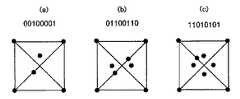
図10は本発明のドットパターンの一例であるGRID1を示す説明図である。
図11はドットパターンの情報ドット及びそれに定義されたデータのビット表示の一例を示す拡大図である。
図12(a)、(b)はキードットを中心に配置した情報ドットを示す説明図である。FIG. 10 is an explanatory diagram showing GRID1, which is an example of the dot pattern of the present invention.
FIG. 11 is an enlarged view showing an example of dot display information dots and bit display of data defined therein.
FIGS. 12A and 12B are explanatory diagrams showing information dots arranged around key dots.
本発明のドットパターンを用いた情報入出力方法は、ドットパターン1の生成と、そのドットパターン1の認識と、このドットパターン1から情報及びプログラムを出力する手段とからなる。即ち、ドットパターン1をカメラ(本実施形態では図2の撮像部23)により画像データとして取り込み、まず、基準格子点ドット4を抽出し、次に本来基準格子点ドット4がある位置にドットが打たれていないことによってキードット2を抽出し、次に情報ドット3を抽出することによりデジタル化して情報領域を抽出して情報の数値化を図り、その数値情報より、このドットパターン1から情報及びプログラムを出力させる。例えば、このドットパターン1から音声等の情報やプログラムを、情報出力装置、パーソナルコンピュータ、PDA又は携帯電話等(本実施形態では図3の主制御部27)に出力させる。 The information input / output method using a dot pattern according to the present invention includes generation of a
本発明のドットパターン1の生成は、ドットコード生成アルゴリズムにより、音声等の情報を認識させるために微細なドット、即ち、キードット、情報ドット、基準格子点ドット4を所定の規則に則って配列する。
図10に示すように、情報を表すドットパターン1のブロックは、キードット2を基準に5×5の基準格子点ドット4を配置し、4点の基準格子点ドット4に囲まれた中心の仮想格子点5の周囲に情報ドット3を配置する。
このブロックには任意の数値情報が定義される。なお、図10の図示例では、ドットパターン1のブロック(太線枠内)を4個並列させた状態を示している。ただし、ドットパターン1は4ブロックに限定されないことはもちろんである。The
As shown in FIG. 10, in the block of
Arbitrary numerical information is defined in this block. Note that the illustrated example of FIG. 10 shows a state in which four blocks (inside the thick line frame) of the
1つのブロックに1つの対応した情報及びプログラムを出力させ、又は、複数のブロックに1つの対応した情報及びプログラムを出力させることができる。 One corresponding information and program can be output to one block, or one corresponding information and program can be output to a plurality of blocks.
基準格子点ドット4は、カメラでこのドットパターン1を画像データとして取り込む際に、そのカメラのレンズの歪みや斜めからの撮像、紙面の伸縮、媒体表面の湾曲、印刷時の歪みを矯正することができる。具体的には歪んだ4点の基準格子点ドット4を元の正方形に変換する補正用の関数(Xn,Yn)=f(Xn’,Yn’)を求め、その同一の関数で情報ドット3を補正して、正しい情報ドット3のベクトルを求める。 When the
キードット2は、図10に示すように、ブロックの四隅の角部にある4個の基準格子点ドット4を一定方向にずらして配置したドットである。このキードット2は、情報ドット3を表す1ブロック分のドットパターン1の代表点である。例えば、ドットパターン1のブロックの四隅の角部にある基準格子点ドット4を上方に0.1mmずらしたものである。情報ドット3がX,Y座標値を表す場合に、キードット2を下方に0.1mmらした位置が座標点となる。ただし、この数値はこれに限定されずに、ドットパターン1のブロックの大小に応じて可変し得るものである。 As shown in FIG. 10, the
情報ドット3は種々の情報を認識させるドットである。この情報ドット3は、キードット2を代表点にして、その周辺に配置すると共に、4点の基準格子点ドット4で囲まれた中心を仮想格子点5にして、これを始点としてベクトルにより表現した終点に配置したものである。例えば、この情報ドット3は、基準格子点ドット4に囲まれ、図11に示すように、その仮想格子点5から0.1mm離れたドットは、ベクトルで表現される方向と長さを有するために、時計方向に45度ずつ回転させて8方向に配置し、3ビットを表現する。したがって、1ブロックのドットパターン1で3ビット×16個=48ビットを表現することができる。 The information dot 3 is a dot for recognizing various information. The information dot 3 is arranged around the
なお、図示例では8方向に配置して3ビットを表現しているが、これに限定されずに、16方向に配置して4ビットを表現することも可能であり、種々変更できることはもちろんである。 In the illustrated example, 3 bits are expressed by arranging in 8 directions. However, the present invention is not limited to this, and 4 bits can be expressed by arranging in 16 directions. Of course, various changes can be made. is there.
キードット2、情報ドット3又は基準格子点ドット4のドットの径は、見栄えと、紙質に対する印刷の精度、カメラの解像度及び最適なデジタル化を考慮して、0.03〜0.05mm程度が望ましい。 The diameter of the
また、撮像面積に対する必要な情報量と、各種ドット2,3,4の誤認を考慮して基準格子点ドット4の間隔は縦・横0.3〜0.5mm前後が望ましい。基準格子点ドット4及び情報ドット3との誤認を考慮して、キードット2のずれは格子間隔の20%前後が望ましい。 In addition, in consideration of a necessary amount of information with respect to the imaging area and misidentification of
この情報ドット3と、4点の基準格子点ドット4で囲まれた仮想格子点との間隔は、隣接する仮想格子点5間の距離の10〜30%程度の間隔であることが望ましい。情報ドット3と仮想格子点5間の距離がこの間隔より近いと、ドットを配置する格子を容易に把握でき、定義されたドットコード値をリバースできることから、セキュリティ性に欠け、格子状の模様が発生する。逆に、情報ドット3と仮想格子点5間の距離がこの間隔より遠いと、隣接するいずれの仮想格子点5を中心にしてベクトル方向性を持たせた情報ドット3であるかの認定が困難になり、情報ドットの配置パターンによっては模様が発生し、ドットパターン1として見苦しくなるからである。 The interval between the
例えば,情報ドット3は、図12(a)に示すように、キードットを中心にブロック中心から時計回りでI1からI16を配置する格子間隔は0.3〜0.5mmであり、1.2mm×1.2mm〜2mm×2mmで3ビット×16=48ビットを表現する。 For example, as shown in FIG. 12A, the information dot 3 has a grid interval of 0.3 to 0.5 mm and 1.2 mm in which I1 to I16 are arranged clockwise from the block center around the key dot. X 1.2 mm to 2 mm x 2 mm represents 3 bits x 16 = 48 bits.
なお、ブロック内に個々に独立した情報内容を有し、かつ他の情報内容に影響されないサブブロックをさらに設けることができる。図12(b)はこれを図示したものであり、4つの情報ドット3で構成されるサブブロック[I1、I2、I3、I4]、[I5、I6、I7、I8]、[I9、I10、I11、I12]、[I13、I14、I15、I16]は各々独立したデータ(3ビット×4=12ビット)が情報ドット3に展開されるようになっている。このようにサブブロックを設けることにより、エラーチェックをサブブロック単位で容易に行うことができる。 In addition, it is possible to further provide sub-blocks having independent information contents in the block and not affected by other information contents. FIG. 12B illustrates this, and sub-blocks [I1, I2, I3, I4], [I5, I6, I7, I8], [I9, I10, I11, I12] and [I13, I14, I15, I16] are such that independent data (3 bits × 4 = 12 bits) is developed on the
情報ドット3のベクトル方向(回転方向)は、30度〜90度毎に均等に定めるのが望ましい。 It is desirable that the vector direction (rotation direction) of the
図13は、情報ドット3及びそこに定義されたデータのビット表示の例であり、他の形態を示すものである。 FIG. 13 is an example of the bit display of the
また、情報ドット3について基準格子点ドット4で囲まれた仮想格子点5から長・短の2種類を使用し、ベクトル方向を8方向とすると、4ビットを表現することができる。このとき、長い方が隣接する仮想格子点5間の距離の20〜30%程度、短い方は10〜20%程度が望ましい。ただし、長・短の情報ドット3の中心間隔は、これらのドットの径より長くなることが望ましい。 In addition, using two types of
4点の基準格子点ドット4で囲まれた情報ドット3は、見栄えを考慮し、1ドットが望ましい。しかし、見栄えを無視し、情報量を多くしたい場合は、1ベクトル毎に、1ビットを割り当て情報ドット3を複数のドットで表現することにより、多量の情報を有することができる。例えば、同心円8方向のベクトルでは、4点の格子ドット4に囲まれた情報ドット3で28の情報を表現でき、1ブロックの情報ドット16個で2128となる。The information dot 3 surrounded by the four reference
図14は、情報ドット及びそこに定義されたデータのビット表示の例であり、(a)はドットを2個、(b)はドットを4個及び(c)はドットを5個配置したものを示すものである。 FIG. 14 shows an example of information dot and bit display of data defined therein, where (a) shows two dots, (b) shows four dots, and (c) shows five dots. Is shown.
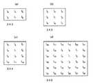
図15は、ドットパターンの変形例を示すものであり、(a)は情報ドット6個配置型、(b)は情報ドット9個配置型、(c)は情報ドット12個配置型、(d)は情報ドット36個配置型の概略図である。 FIG. 15 shows a modification of the dot pattern, where (a) is a six information dot arrangement type, (b) is a nine information dot arrangement type, (c) is a 12 information dot arrangement type, (d ) Is a schematic diagram of a 36 information dot arrangement type.
図10と図12に示すドットパターン1は、1ブロックに16個(4×4)の情報ドット3を配置した例を示している。しかし、この情報ドット3は1ブロックに16個配置することに限定されずに、種々変更することができる。例えば、必要とする情報量の大小又はカメラの解像度に応じて、情報ドット3を1ブロックに6個(2×3)配置したもの(a)、情報ドット3を1ブロックに9個(3×3)配置したもの(b)、情報ドット3を1ブロックに12個(3×4)配置したもの(c)、又は情報ドット3を1ブロックに36個配置したもの(d)がある。 The
図16(a)及び(b)は、図10〜図15で説明したドットパターンにおいて、3×3=9個の格子領域で構成されるブロックのドットパターンにおいて、特定の格子領域(ディレクション領域)だけ情報ドット3の配置方向を他の格子領域(ディレクション領域)と変えることによって、ブロックの方向を定義したものである。 FIGS. 16A and 16B show specific lattice areas (direction areas) in the dot pattern of the block composed of 3 × 3 = 9 lattice areas in the dot patterns described in FIGS. Only by changing the arrangement direction of the
即ち、図16(a)において、左下の格子領域34a、中央の格子領域34b、左下の格子領域34cは中心から縦横方向に情報ドット3が配置され、その他の格子領域では中心から斜め方向に情報ドット3が配置されている。このように格子領域34a,34b,34cを配置することでこの格子領域を結ぶ三角形の形状、即ち、底辺34a,34cに対する頂点34bの関係から、当該ブロックが上向きであることが認識できる。 That is, in FIG. 16A, the
このように、ブロック中の情報ドット3の配置方向を変更した(中心から縦横方向に情報ドットを配置した)格子領域34a,34b,34cの配置関係(ここでは三角形)によってブロックの方向を定義することができる。これによって、ブロック中の全ての格子領域に情報ドット3を配置することができるため、ブロックの方向を定義するために格子領域を犠牲にすることがなく、全ての格子領域に情報ドット3を配置することができる。 As described above, the direction of the block is defined by the arrangement relationship (here, a triangle) of the
なお、図17(b)は、図17(a)に示したブロックを縦横方向に2個ずつ連結したものである。 In FIG. 17B, two blocks shown in FIG. 17A are connected in the vertical and horizontal directions.
なお、ドットパターンを1個だけカードCの裏面に印刷する場合については、格子間の距離が約15mm、ドットの大きさがドット間距離の約15%程度が望ましい。従って、2mm乃至2.5mmが望ましいが、これに限定されるものではない。撮像した画像におけるドット間距離は14ピクセル以上あることが望ましい。 When only one dot pattern is printed on the back surface of the card C, it is desirable that the distance between the lattices is about 15 mm and the dot size is about 15% of the distance between the dots. Therefore, 2 mm to 2.5 mm is desirable, but not limited thereto. The inter-dot distance in the captured image is desirably 14 pixels or more.
図18(a)は、カードCの角度を求める方法について説明した図である。また、同図(b)はカード裏面に印刷されるドットパターンの例を示した図である。
なお、格子点ドットを結ぶ直線はドットパターンの把握のための便宜上表示したもので、実際のドットパターンにはこのような格子線は印刷されていない。FIG. 18A is a diagram illustrating a method for obtaining the angle of the card C. FIG. 2B shows an example of a dot pattern printed on the back side of the card.
Note that the straight lines connecting the grid point dots are displayed for convenience in understanding the dot pattern, and such grid lines are not printed in the actual dot pattern.
同図に示すように、撮影の向き、即ちフレームバッファのy方向と、ドットパターンの向きとがなす角度をαとし、これをカードの角度とする。そして、基準格子点ドットP1の座標を(x1、y1)、P2の座標を(x2,y2)とし、P1P2間の距離、即ち基準格子点ドット同士の間隔をlとする。 As shown in the figure, the angle between the shooting direction, that is, the y direction of the frame buffer and the direction of the dot pattern is α, and this is the card angle. The coordinates of the reference grid point dot P1 are (x1, y1), the coordinates of P2 are (x2, y2), and the distance between P1P2, that is, the interval between the reference grid point dots is 1.
まず、x座標によるθの確定を行う。ここでθとは、0≦x1−x2の場合、
θ1=|sin-1{(x1-x2)/l}|、若しくは、θ2=180-|sin-1{(x1-x2)/l}|となる。First, θ is determined by the x coordinate. Here, θ is 0 ≦ x1−x2,
θ1 = | sin−1 {(x1−x2) / l} | or θ2 = 180− | sin−1 {(x1−x2) / l} |.
また、0>x1-x2の場合、
θ1=180+|sin-1{(x2-x1)/l}|、若しくは、θ2=360-|sin-1{(x2-x1)/l}|となる。If 0> x1-x2,
θ1 = 180 + | sin−1 {(x2−x1) / l} | or θ2 = 360− | sin−1 {(x2−x1) / l} |.
次に、y座標によるθの確定を行う。ここで、θとは、0≦y1-y2の場合、
θ1=|cos-1{(y1-y2)/l}|、若しくは、θ2=360-|cos-1{(y1-y2)/l}|となる。Next, θ is determined by the y coordinate. Where θ is 0 ≦ y1-y2
θ1 = | cos-1 {(y1-y2) / l} | or θ2 = 360- | cos-1 {(y1-y2) / l} |.
また、0>y1-y2の場合、
θ1=180-|cos-1{(y2-y1)/l}|、若しくは、θ2=180+|cos-1{(y2-y1)/l}|となる。If 0> y1-y2,
θ1 = 180− | cos−1 {(y2−y1) / l} | or θ2 = 180 + | cos−1 {(y2−y1) / l} |.
ここで、x座標及びy座標によるθは、夫々2つの解(θ1,θ2)があり、x座標及びy座標により求められる解が同一となるθを選択し、それをαとする。 Here, there are two solutions (θ1, θ2) for θ based on the x coordinate and the y coordinate, respectively, and θ which is the same as the solution determined by the x coordinate and the y coordinate is selected and is defined as α.
図19は、カード配置パネル11上にカードCが載置されている状態を上から見た平面図である。 FIG. 19 is a plan view of the state in which the card C is placed on the
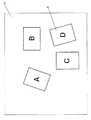
プレイヤは、AからDまでの4枚のカードCを、カード配置パネル11上の任意の位置に載置することが可能である。 The player can place the four cards C from A to D at arbitrary positions on the
図20は、カード配置パネル11上に載置されているカードCを、カード配置パネル下面側に配置されたセンサユニット30での撮像画像を示した図である。
即ち、図20の撮像画像は、1つのセンサユニット30、即ち、1台の撮像部23の撮像領域(サブ解析領域)内に4枚のカードCA乃至CDが配置されている様子を示している。FIG. 20 is a diagram illustrating a captured image of the card C placed on the
That is, the captured image in FIG. 20 shows a state in which four cards CA to CD are arranged in one sensor unit 30, that is, in the imaging region (sub-analysis region) of one
上述した如く、センサユニット30は、台座部12(図1や図2)の筐体内の下部に設けられ、カード配置パネル11の裏面を撮影する。
したがって、センサユニット30で撮影される画像は、図20と上下左右が逆になったものであり、また、カード裏面に印刷されたドットコードが撮影されている。As described above, the sensor unit 30 is provided in the lower part of the housing of the pedestal 12 (FIGS. 1 and 2), and photographs the back surface of the
Therefore, the image photographed by the sensor unit 30 is upside down and left and right in FIG. 20, and the dot code printed on the back side of the card is photographed.
図21は、カードCの有無を判定するための画素マトリクスを示したものである。この画素マトリクスは、16ピクセル×16ピクセルで1つのセルが構成されており、所定のピクセル(同図でハッチングが施されたピクセル)がチェック画素として機能する。 FIG. 21 shows a pixel matrix for determining the presence or absence of the card C. In this pixel matrix, one cell is composed of 16 pixels × 16 pixels, and predetermined pixels (hatched pixels in the figure) function as check pixels.
即ち、所定間隔毎(ここでは5ピクセル毎)に設定されたチェック画素群の明度を検出し、当該明度が予め設定された閾値以上の明度であったときに当該画素マトリクス上に媒体が載置されていると判定するようになっている。 That is, the brightness of the check pixel group set at predetermined intervals (here, every 5 pixels) is detected, and the medium is placed on the pixel matrix when the brightness is not less than a preset threshold value. It is judged that it is being done.
以下、具体的に説明する。 This will be specifically described below.
まず、センサユニット30に設けられたCPUは、サブ解析領域(撮像領域)を、後述の図22に示す如く、縦18×横22のセルに分割する。このセルを、さらに縦16×横16のピクセルに分割する。そして、ピクセルのうち、図21でハッチングを施した部分のブライトレベル(明度)を測定する。ブライトレベルは、0から255の256段階で表される。そして、任意の閾値を設定し、ブライトレベルが閾値以上であれば、その位置にカード又は物体若しくは手が載置されていると判定する。ただし、ブライトレベルが255の場合は、ホワイトノイズであるため、カード等が載置されているとは判定しない。 First, the CPU provided in the sensor unit 30 divides the sub-analysis region (imaging region) into 18 vertical × 22 horizontal cells as shown in FIG. This cell is further divided into 16 × 16 pixels. Then, the brightness level (brightness) of the portion hatched in FIG. 21 among the pixels is measured. The bright level is expressed in 256 levels from 0 to 255. An arbitrary threshold value is set, and if the brightness level is equal to or higher than the threshold value, it is determined that a card, an object, or a hand is placed at that position. However, when the brightness level is 255, it is white noise, and it is not determined that a card or the like is placed.
図22は、カードCのコードを解析する方法を説明した図である。 FIG. 22 is a diagram illustrating a method of analyzing the code of the card C.
まず、上述した如く、サブ解析領域(撮像領域)を縦18×横22のセルに分割する。そして、センサユニット30によって一番左上のセルから右方向にセルを走査していく。ここで、カードCのドット以外の部分は、赤外線を反射するパターンが採用されているものとすると、カードCが載置されていない領域よりも明るく撮影される。そこで、センサユニット30で走査していき、明るく撮影されているセルを探索する。明るく撮影されているセルであれば、そこにカードCが載置されていると判断される。そして、上述した方法により、ドットの有無を判定する。明るい領域の探索とドットの有無の判定を順次行うことにより、カード面に印刷されたドットコードが読み取られる。 First, as described above, the sub-analysis region (imaging region) is divided into 18 × 22 cells. Then, the sensor unit 30 scans the cells in the right direction from the upper left cell. Here, assuming that a pattern that reflects infrared rays is adopted for the portions other than the dots of the card C, the image is taken brighter than the area where the card C is not placed. Therefore, the sensor unit 30 scans and searches for a brightly photographed cell. If the cell is brightly photographed, it is determined that the card C is placed there. Then, the presence or absence of dots is determined by the method described above. The dot code printed on the card surface is read by sequentially searching for a bright area and determining the presence or absence of dots.
この方法によれば、明るい領域にカードCがあると判断し、その領域のみドットの検出をすることになるため、ドットを検出するのに要する時間を短縮することができる。 According to this method, since it is determined that the card C is in a bright area and dots are detected only in that area, the time required to detect dots can be shortened.
ここで、本実施形態では、カードCが置かれたセル(16×16ピクセル)の部分だけでドットの検出を行うため、計算の効率化ができるため、ドットパターンの読取時間を高速化することができる。 Here, in this embodiment, since dots are detected only in the portion of the cell (16 × 16 pixels) in which the card C is placed, calculation efficiency can be improved, so that the dot pattern reading time is increased. Can do.
図23は、カード配置パネル11上(ステージ面上)に載置されたカードCの位置及び角度を認識する方法を説明する図である。
なお、上述したようにここでは、1つのセンサユニット30が担当する1つのサブ解析領域(撮像領域)のローカル座標系を用いて説明する。ただし、実際には、複数のサブ解析領域が重複領域を含めて配置された解析領域全体において、カード解析全体座標系で処理がなされる場合がある。FIG. 23 is a diagram illustrating a method for recognizing the position and angle of the card C placed on the card placement panel 11 (on the stage surface).
As described above, here, description will be made using the local coordinate system of one sub-analysis region (imaging region) that is handled by one sensor unit 30. However, in practice, processing may be performed in the overall card analysis coordinate system in the entire analysis region in which a plurality of sub-analysis regions are arranged including the overlapping region.
まず、前述した方法により、センサユニット30の撮像部23がカード面のドットパターンを撮像すると、当該センサユニット30のユニット制御部24は、このドットパターンに対応したコード値を検出する。
そして、ユニット制御部24は、該コード値を検出したら、次にキードットを探索する。
そして、ユニット制御部24は、カード中心のx、y座標を算定し、これをカードの位置とする。カードの位置は、配置パネルの右下(撮像される際は左上)を基準にしたx、y座標で表される。即ち、これにより、カードの位置を検出することにより、カードの中心を算出し、カード中心のx、y座標を求める。これにより、カードの位置が算出される。即ち、図23では、カードCAの座標は(xa,ya),カードCBの座標は(xb,yb)、カードCCの座標は(xc,yc)、カードCDの座標は(xd,yd)となる。First, when the
When the
Then, the
また、カード中心とキードットとを結んだ直線と、カード配置パネルの垂直方向との角度をαとし、これをカードの向きとする。カードの角度は、前述した方法により算定される。 The angle between the straight line connecting the card center and the key dot and the vertical direction of the card placement panel is α, and this is the card orientation. The card angle is calculated by the method described above.
図24は、カード配置パネル11上(ステージ面上)で、プレイヤがカードCを移動させた際に、移動した角度及び移動量を算出する方法を説明した図である。 FIG. 24 is a diagram illustrating a method of calculating the angle and amount of movement when the player moves the card C on the card arrangement panel 11 (on the stage surface).
カードCが移動したことをどのように認識するかについては、例えば、センサユニット30によって、上述したように、カードCが載置された画素マトリクスが検出されたら、ドットパターンの中からコード値を読み込むと共に、キードットを探すという手法を採用する。
これにより、カード配置パネル11上でのカードCの向きが分かる。カード配置パネル11上でプレイヤがカードCを移動させたときにはカード配置パネル11上を同じコード値が移動することになる。したがって、この所定時間毎にこのコード値が再現される位置を軌跡として結べば、カードCが移動されたこと、その移動方向、移動軌跡等を認識できる。
なお、図25のように、非軸対称のドットパターンを使用すれば、基準ドットで方向とデータの領域を定義でき、キードットの配置は必要ない。同図(a)は1個のドットパターンを示す図、(b)は、同図(a)の一点鎖線の箇所の拡大図である。As to how to recognize that the card C has moved, for example, when the sensor unit 30 detects the pixel matrix on which the card C is placed as described above, the code value is determined from the dot pattern. The method of searching for key dots is adopted while reading.
Thereby, the orientation of the card C on the
If a non-axisymmetric dot pattern is used as shown in FIG. 25, the direction and data area can be defined by the reference dot, and no key dot arrangement is required. FIG. 4A is a diagram showing one dot pattern, and FIG. 4B is an enlarged view of a dot-dash line portion in FIG.
また、センサユニット30のユニット制御部24においては、移動前と移動後の、キードットや基準ドットの向きの差により、移動による回転角が分かる。また、移動量、移動時間を計算できる。 Further, in the
このように、カードCの位置によってカード所持者のパワーを可変としたり、移動量や移動時間をパラメータとしてゲームを進めてもよい。 As described above, the power of the cardholder may be made variable depending on the position of the card C, or the game may be advanced using the amount of movement and the time of movement as parameters.
以下、具体的に図24を説明する。 Hereinafter, FIG. 24 will be specifically described.
同図に示すように、プレイヤが、カードCA,CB,CC,CDを夫々移動させたとする。
このとき、カードCAの中心は(xa,ya)から(xa’,ya’)に、カードCBの中心は(xb,yb)から(xb’,yb’)に、カードCCの中心は(xc,yc)から(xc’,yc’)に、カードCDの中心は(xd,yd)から(xd’,yd’)に夫々移動したとする。
その際に、カード配置パネル11に対する角度は、カードCAがαaからα’aに、カードCBがαbからα’bに、カードCCがαcからα’cに、カードCDがαdからα’dに、夫々変化したとする。このとき、カードCAの移動量laは、
la=√{(xa’−xa)2+(ya’−ya)2}
となる。As shown in the figure, it is assumed that the player moves the cards CA, CB, CC, and CD, respectively.
At this time, the center of the card CA is (xa, ya) to (xa ′, ya ′), the center of the card CB is (xb, yb) to (xb ′, yb ′), and the center of the card CC is (xc). , Yc) to (xc ′, yc ′), and the center of the card CD is moved from (xd, yd) to (xd ′, yd ′).
At this time, the angles with respect to the
la = √ {(xa′−xa) 2+ (ya′−ya) 2}
It becomes.
また、回転角θaは、
θa=α’a−αa
となる。The rotation angle θa is
θa = α′a−αa
It becomes.
また、カードの移動前の時刻をTa、移動後の時刻をTa’とすると、移動に要した時間taは
ta=Ta’−Ta
となる。Further, if the time before the card movement is Ta and the time after the movement is Ta ′, the time ta required for the movement is ta = Ta′−Ta.
It becomes.
カードCB,CC,CDについても同様である。 The same applies to the cards CB, CC, and CD.
例えば、プレイヤがカードCを移動させると、カードCの移動量、回転角及び移動時間がパラメータとなり、カードCのパワーが変化するような遊技が考えられる。即ち、カードCを移動させることにより、カードCの強弱が変化することになる。 For example, when the player moves the card C, a game in which the power of the card C changes due to the movement amount, rotation angle, and movement time of the card C as parameters can be considered. That is, by moving the card C, the strength of the card C changes.
図26は、カードCの軌跡をパラメータとする場合を説明した図であり、(a)は円状にカードCを移動させた場合、(b)は四角形を描くようにカードCを移動させた場合である。 FIG. 26 is a diagram for explaining the case where the trajectory of the card C is used as a parameter. FIG. 26A shows a case where the card C is moved in a circle, and FIG. 26B shows a case where the card C is moved so as to draw a square. Is the case.
本発明においては、プレイヤがカードCを移動させた場合の軌跡もパラメータとすることができる。例えば、軌跡の形状をパラメータとすることができる。即ち、プレイヤが(a)に示すように曲線状にカードを移動させるか、(b)に示すように直線状に移動させるかにより、カードCの属性等のパラメータを変化させてもよい。 In the present invention, the trajectory when the player moves the card C can also be used as a parameter. For example, the shape of the trajectory can be used as a parameter. That is, parameters such as attributes of the card C may be changed depending on whether the player moves the card in a curved line as shown in (a) or moves in a straight line as shown in (b).
上記の場合には、カードCが一定時間以上静止をしたら、軌跡が終了したとみなすことができる。また、プレイヤがカードCをカード配置パネル11から離したら軌跡が終了した、とすることができる。 In the above case, if the card C is stationary for a certain time or more, it can be considered that the trajectory has ended. Further, it can be assumed that the trajectory is ended when the player releases the card C from the
ステージ面(カード配置パネル11面)上で認識する媒体としては、前述のカードのほか、オペレータまたはプレイヤ自身の指先であってもよい。このようにステージ面上で指先がタッチされたときには、タッチされた部分のステージ面の明度が変化するために、指先であることが認識可能である。具体的には、図27、図28で説明する。
図27(a)に示す如く、プレイヤ又はオペレータがカードを載置したり、指先で、ステージ面上をタッチしたりすることにより、ゲームが行われる。同図(b)は、この状態をステージ面の下から見た状態を示した図である。
同図(c)は媒体の形状を認識する方法を説明した図である。赤外線を撮影した画像には、タッチした位置が撮像されており、所定の方法でタッチ領域を判定し、さらに、タッチ領域の重心や図心などを求める所定の方法で、タッチ位置中心座標を求めることができる。一例としては、任意の閾値を超える明度の変化の状況から領域をステージ面との接触面とする。閾値は、絶対値でもよいし、周辺の明るさによって変化するダイナミック閾値でもよいし、周辺の明るさに対する比を閾値として使用してもよい。ここでは、1つの接触面は、記憶領域を構成する画素のうち、閾値を超えた画素のうち、閾値を超えた画素の縦・横・上・下のいずれか1個以上が連続している領域とする。
具体的には、同図(c)に示した、太線で囲まれた領域が、閾値を超えた画素の領域であり、媒体の形状を示している。The medium recognized on the stage surface (the
As shown in FIG. 27A, the game is played when the player or the operator places a card or touches the stage surface with a fingertip. FIG. 2B is a diagram showing a state in which this state is viewed from below the stage surface.
FIG. 4C is a diagram for explaining a method for recognizing the shape of the medium. The touched position is imaged in the infrared image, the touch area is determined by a predetermined method, and the center coordinates of the touch position are determined by a predetermined method for determining the center of gravity, centroid, etc. of the touch area. be able to. As an example, the region is set as a contact surface with the stage surface from the situation of a change in brightness exceeding an arbitrary threshold value. The threshold value may be an absolute value, a dynamic threshold value that varies depending on ambient brightness, or a ratio to ambient brightness may be used as the threshold value. Here, one contact surface has one or more of vertical, horizontal, upper, and lower pixels that exceed the threshold among the pixels that constitute the storage area that exceed the threshold. This is an area.
Specifically, an area surrounded by a thick line shown in FIG. 5C is a pixel area exceeding the threshold value, and indicates the shape of the medium.
また、同図(c)により認識された画像によって媒体の図心を算出して、当該図心の座標に対応したオペレーションを実行するようにすることも可能である。以下、図心を算出する方法について説明する。
まず、閾値を超えた画素マトリックスのX座標の数値を求める。各行におけるX座標の値は、xmsns〜xmeneである。そして、すべてのX座標の数値を加算する。加算して得られた値を、画素マトリックスの個数で割ることにより得られた値が、図心のX座標の値となる。
図心のY座標も、同様の方法により算出される。It is also possible to calculate the centroid of the medium from the image recognized in FIG. 10C and execute an operation corresponding to the coordinates of the centroid. Hereinafter, a method for calculating the centroid will be described.
First, the numerical value of the X coordinate of the pixel matrix exceeding the threshold is obtained. The value of X coordinates in each rowarex msns~x mene. Then, the numerical values of all X coordinates are added. A value obtained by dividing the value obtained by the addition by the number of pixel matrices becomes the value of the X coordinate of the centroid.
The Y coordinate of the centroid is also calculated by a similar method.
なお、本発明は、上述の実施形態に限定されるものではなく、本発明の目的を達成できる範囲での変形、改良等は本発明に含まれるものである。 In addition, this invention is not limited to the above-mentioned embodiment, The deformation | transformation in the range which can achieve the objective of this invention, improvement, etc. are included in this invention.
例えば、上述の例では、カード配置パネル11にカードCが配置されたが、特にこれに限定されない。
即ち、本発明は、カード配置パネル11を含め、裏面側から照射された光のうち少なくとも一部の第1光を表面に通過させると共に、所定の媒体を前記表面側に配置可能な平面板に対して適用できる。
換言すると、平面板の表面側には、カードCを含め任意の媒体を配置することができる。
さらに、発光部から発光される対象は、赤外光に特に限定されず、可視光であってもよい。For example, in the above-described example, the card C is arranged on the
That is, the present invention includes a
In other words, any medium including the card C can be arranged on the surface side of the flat plate.
Furthermore, the target emitted from the light emitting unit is not particularly limited to infrared light, and may be visible light.
つまり、本発明は、次の構成を有すれば足り、上述の実施形態を含め多種多様な実施形態を取ることができる。
即ち、本発明が適用される光学装置は、
裏面側から照射された光のうち少なくとも一部の第1光を表面に通過させると共に、所定の媒体を前記表面側に配置可能な平面板と、
前記平面板の裏面側から前記光を照射する発光部と、
前記平面板を介して、前記媒体で反射された前記第1光で露光することで、前記媒体を撮像する撮像部と、
前記発光部から照射された光のうち前記平面板にて反射された第2光の、前記撮像部への入射を禁止するように、前記発光部から照射された光の照射方向を規制する規制部と、
を備える。
これにより、複数の撮像部を設けることが容易に可能になり、サイズが大きなステージ面(平面板)に対応することができる。つまり、ステージ面の大きさに応じて撮像部を適切な個数用意することで、任意のサイズのステージ面を有するボードゲームを容易に実現可能にすることができる。That is, the present invention only needs to have the following configuration, and can take a wide variety of embodiments including the above-described embodiments.
That is, the optical apparatus to which the present invention is applied is
A flat plate that allows at least a portion of the first light of the light irradiated from the back side to pass through the surface, and can arrange a predetermined medium on the surface side;
A light emitting unit for irradiating the light from the back side of the flat plate;
An imaging unit that images the medium by exposing with the first light reflected by the medium through the plane plate;
Regulation that regulates the irradiation direction of the light emitted from the light emitting unit so that the second light reflected by the flat plate out of the light emitted from the light emitting unit is prohibited from entering the imaging unit. And
Is provided.
Accordingly, it is possible to easily provide a plurality of imaging units, and it is possible to deal with a large stage surface (planar plate). That is, by preparing an appropriate number of imaging units according to the size of the stage surface, a board game having a stage surface of an arbitrary size can be easily realized.
また例えば、上述の実施形態では、カードCの位置等が認識されたが、カードCを含め媒体の任意の情報を認識することができる。
例えば、撮像部により撮像された媒体の特徴、又は当該媒体に付された情報を認識することができる。ここで、媒体の特徴としては、例えば媒体の形状と大きさのうち少なくとも一方を認識することができる。For example, in the above-described embodiment, the position of the card C and the like are recognized, but any information on the medium including the card C can be recognized.
For example, it is possible to recognize characteristics of the medium imaged by the imaging unit or information attached to the medium. Here, as a characteristic of the medium, for example, at least one of the shape and size of the medium can be recognized.
さらに、媒体には、画像、文字、図形、若しくは記号又はこれらの結合が形成されているようにすることができる。この場合、画像、文字、図形、記号又はこれらの結合を認識することができる。 Further, the medium can be formed with images, characters, graphics, symbols, or combinations thereof. In this case, an image, a character, a graphic, a symbol, or a combination thereof can be recognized.
ここで、媒体は、第1光の反射率が他と異なる部分を少なくとも一部に含むようにすることができる。この場合、第1光の反射率が他と異なる部分を認識することができる。
例えば、媒体には、第1光の反射率が他と異なる部分として、画像、文字、図形、若しくは記号又はこれらの結合が形成されているようにすることができる。Here, the medium may include at least part of a portion where the reflectance of the first light is different from the others. In this case, a portion where the reflectance of the first light is different from the others can be recognized.
For example, an image, a character, a figure, a symbol, or a combination thereof may be formed on the medium as a portion where the reflectance of the first light is different from the others.
ここで例えば、媒体の第1光の反射率が他と異なる部分は、第1光を反射させるドットであり、第1光を非反射させる媒体の面に、複数のドットからなるドットパターンが形成されているようにしてもよい。この場合、ドットパターンが認識される。 Here, for example, the portion where the reflectance of the first light of the medium is different from the others is the dots that reflect the first light, and a dot pattern composed of a plurality of dots is formed on the surface of the medium that does not reflect the first light. You may be made to do. In this case, a dot pattern is recognized.
或いは例えば。媒体の第1光の反射率が他と異なる部分は、第1光を非反射させるドットであり、第1光を反射させる媒体の面に、複数のドットからなるドットパターンが形成されているようにしてもよい。この場合も、ドットパターンが認識される。 Or for example. The part where the reflectance of the first light of the medium is different from the others is dots that do not reflect the first light, and a dot pattern composed of a plurality of dots is formed on the surface of the medium that reflects the first light. It may be. Also in this case, the dot pattern is recognized.
また例えば、本発明が適用される光学装置は、
撮像部を複数個備え、
平面板において、複数の撮像部の夫々により撮像される各撮像領域は、少なくとも1つの他の撮像部により撮像される撮像領域と重複する重複領域を有している、
ようにしてもよい。Also, for example, an optical device to which the present invention is applied is
A plurality of imaging units,
In the plane plate, each imaging area imaged by each of the plurality of imaging units has an overlapping area overlapping with the imaging area imaged by at least one other imaging unit,
You may do it.
また例えば、本発明が適用される光学装置は、
発光部を複数個備え、
平面板は、複数の発光部により照射され、
規制部は、さらに、当該規制部が無い場合と比較して、平面板における光量差を抑制すると共に、光量差がある領域では光量の変化の度合を抑制するように、複数の発光部のうち少なくとも一部から照射された光の照射方向を規制する、
ようにしてもよい。Also, for example, an optical device to which the present invention is applied is
It has a plurality of light emitting parts,
The plane plate is irradiated by a plurality of light emitting units,
The restricting unit further suppresses the light amount difference in the flat plate as compared to the case where the restricting unit is not provided, and among the plurality of light emitting units so as to suppress the degree of change in the light amount in the region where the light amount difference exists. Regulate the direction of irradiation of light emitted from at least a part,
You may do it.
また例えば、本発明が適用される光学装置は、
前記撮像部の撮像領域を照射する前記発光部の発光中に、当該撮像部を露光させる制御部をさらに備える、
ようにしてもよい。Also, for example, an optical device to which the present invention is applied is
A control unit that exposes the imaging unit during light emission of the light emitting unit that irradiates the imaging region of the imaging unit;
You may do it.
また例えば、本発明が適用される光学装置は、
撮像部による露光期間内の所定時間だけ、当該撮像部の撮像領域を照射する発光部から光を照射させる制御を実行する制御部をさらに備える、
ようにしてもよい。Also, for example, an optical device to which the present invention is applied is
A control unit that executes control to irradiate light from the light emitting unit that irradiates the imaging region of the imaging unit for a predetermined time within the exposure period by the imaging unit;
You may do it.
また例えば、本発明が適用される光学装置は、
複数の撮像部で撮像された画像のうち、媒体の少なくとも一部を被写体として含む画像を1以上用いて、平面板を基準とする座標系で媒体の位置を認識する認識部、
をさらに備えるようにしてもよい。Also, for example, an optical device to which the present invention is applied is
A recognition unit for recognizing the position of the medium in a coordinate system based on a plane plate using one or more images including at least a part of the medium as a subject among images captured by a plurality of imaging units;
May be further provided.
また例えば、平面板は、透過スクリーンの機能を有し、
透過スクリーンに可視光で画像を投影可能なプロジェクタ
をさらに備えるようにしてもよい。For example, the flat plate has a function of a transmission screen,
You may make it further provide the projector which can project an image with visible light on a transmissive screen.
ここで、上述したように、発光部から照射される光は、上述の実施形態の赤外光等非可視光であるようにしてもよい。 Here, as described above, the light emitted from the light emitting unit may be invisible light such as infrared light in the above-described embodiment.
或いは、発光部から照射される光は、白色の可視光であるようにしてもよい。
白色の可視光が採用される場合においては、
本発明が適用される光学装置は、
所定時間(例えば1/1000秒)だけ発光部から光を照射させる制御を実行する制御部と、
撮像部により撮像された画像を用いて、平面板に配置された媒体を認識する認識部と、
をさらに備えると好適である。
この場合、制御部は、さらに、撮像部において光電変換された画像信号を保持するバッファをクリアした後、撮像部の露光タイミングと発光部の照射タイミングとを同期させる制御を実行するようにすると好適である。Or you may make it the light irradiated from a light emission part be white visible light.
When white visible light is used,
An optical device to which the present invention is applied
A control unit that executes control to irradiate light from the light emitting unit for a predetermined time (for example, 1/1000 second);
A recognition unit for recognizing a medium arranged on the flat plate using an image captured by the imaging unit;
It is preferable to further include
In this case, it is preferable that the control unit further executes control to synchronize the exposure timing of the imaging unit and the irradiation timing of the light emitting unit after clearing the buffer that holds the image signal photoelectrically converted in the imaging unit. It is.
上述した一連の処理は、ハードウェアにより実行させることもできるし、ソフトウェアにより実行させることもできる。
一連の処理をソフトウェアにより実行させる場合には、そのソフトウェアを構成するプログラムが、コンピュータ等にネットワークや記録媒体からインストールされる。
コンピュータは、専用のハードウェアに組み込まれているコンピュータであってもよい。また、コンピュータは、各種のプログラムをインストールすることで、各種の機能を実行することが可能なコンピュータ、例えば汎用のパーソナルコンピュータであってもよい。The series of processes described above can be executed by hardware or can be executed by software.
When a series of processing is executed by software, a program constituting the software is installed on a computer or the like from a network or a recording medium.
The computer may be a computer incorporated in dedicated hardware. The computer may be a computer capable of executing various functions by installing various programs, for example, a general-purpose personal computer.
このようなプログラムを含む記録媒体は、プレイヤにプログラムを提供するために装置本体とは別に配布されるリムーバブルメディアにより構成されるだけでなく、装置本体に予め組み込まれた状態でプレイヤに提供される記録媒体等で構成される。リムーバブルメディアは、例えば、磁気ディスク(フロッピディスクを含む)、Blu−ray Disc(ブルーレイディスク)(登録商標)、光ディスク、又は光磁気ディスク等により構成される。光ディスクは、例えば、CD−ROM(Compact Disk−Read Only Memory),DVD(Digital Versatile Disk)等により構成される。光磁気ディスクは、MD(Mini−Disk)、等により構成される。また、装置本体に予め組み込まれた状態でプレイヤに提供される記録媒体は、例えば、プログラムが記録されているROMや、ハードディスク等で構成される。 A recording medium including such a program is not only constituted by a removable medium distributed separately from the apparatus main body in order to provide the program to the player, but is provided to the player in a state of being incorporated in advance in the apparatus main body. It consists of a recording medium. The removable medium is configured by, for example, a magnetic disk (including a floppy disk), a Blu-ray Disc (Blu-ray Disc) (registered trademark), an optical disk, a magneto-optical disk, or the like. The optical disk is composed of, for example, a CD-ROM (Compact Disk-Read Only Memory), a DVD (Digital Versatile Disk), or the like. The magneto-optical disk is configured by an MD (Mini-Disk) or the like. In addition, the recording medium provided to the player in a state of being preliminarily incorporated in the apparatus main body includes, for example, a ROM in which a program is recorded, a hard disk, and the like.
なお、本明細書において、記録媒体に記録されるプログラムを記述するステップは、その順序に沿って時系列的に行われる処理はもちろん、必ずしも時系列的に処理されなくとも、並列的或いは個別に実行される処理をも含むものである。
また、本明細書において、システムの用語は、複数の装置や複数の手段等より構成される全体的な装置を意味するものとする。In the present specification, the step of describing the program recorded on the recording medium is not limited to the processing performed in time series along the order, but is not necessarily performed in time series, either in parallel or individually. The process to be executed is also included.
Further, in the present specification, the term “system” means an overall apparatus configured by a plurality of devices, a plurality of means, and the like.
10・・・光学装置、11・・・カード配置パネル、12・・・台座、21・・・規制部、22・・・短焦点プロジェクタ、23・・・撮像部、24・・・ユニット制御部、25・・・発光部、26・・・ユニット制御部、27・・・主制御部、30・・・センサユニット DESCRIPTION OF
Claims (17)
Translated fromJapanese前記平面板の裏面側から前記光を照射する発光部と、
前記平面板を介して、前記媒体で反射された前記第1光で露光することで、前記媒体を撮像する撮像部と、
前記発光部から照射された光のうち前記平面板にて反射された第2光の、前記撮像部への入射を禁止するように、前記発光部から照射された光の照射方向を規制する規制部と、
を備える光学装置。A flat plate that allows at least a portion of the first light of the light irradiated from the back side to pass through the surface, and can arrange a predetermined medium on the surface side;
A light emitting unit for irradiating the light from the back side of the flat plate;
An imaging unit that images the medium by exposing with the first light reflected by the medium through the plane plate;
Regulation that regulates the irradiation direction of the light emitted from the light emitting unit so that the second light reflected by the flat plate out of the light emitted from the light emitting unit is prohibited from entering the imaging unit. And
An optical device comprising:
をさらに備える請求項1に記載の光学装置。The optical device according to claim 1, further comprising: a recognition unit that recognizes characteristics of the medium imaged by the imaging unit or information attached to the medium.
請求項2に記載の光学装置。The optical device according to claim 2, wherein the recognition unit recognizes at least one of a shape and a size of the medium as a characteristic of the medium.
前記認識部は、前記画像、前記文字、前記図形、前記記号又は前記これらの結合を認識する
請求項3に記載の光学装置。In the medium, an image, a character, a figure, or a symbol or a combination thereof is formed,
The optical device according to claim 3, wherein the recognition unit recognizes the image, the character, the graphic, the symbol, or the combination thereof.
前記認識部は、前記第1光の反射率が他と異なる部分を認識する
請求項4に記載の光学装置。The medium includes at least part of a portion where the reflectance of the first light is different from the others,
The optical device according to claim 4, wherein the recognition unit recognizes a portion in which the reflectance of the first light is different from the others.
請求項5に記載の光学装置。The optical device according to claim 5, wherein the image, the character, the figure, the symbol, or the combination thereof is formed on the medium as a portion where the reflectance of the first light is different from others.
前記第1光を非反射させる前記媒体の面に、複数の前記ドットからなるドットパターンが形成されており、
前記認識部は、前記ドットパターンを認識する
請求項6に記載の光学装置。A portion where the reflectance of the first light of the medium is different from others is a dot that reflects the first light,
A dot pattern composed of a plurality of the dots is formed on a surface of the medium that does not reflect the first light;
The optical device according to claim 6, wherein the recognition unit recognizes the dot pattern.
前記第1光を反射させる前記媒体の面に、複数の前記ドットからなるドットパターンが形成されており、
前記認識部は、前記ドットパターンを認識する
請求項6に記載の光学装置。The portion where the reflectance of the first light of the medium is different from the others is a dot that makes the first light non-reflective,
A dot pattern composed of a plurality of the dots is formed on the surface of the medium that reflects the first light,
The optical device according to claim 6, wherein the recognition unit recognizes the dot pattern.
前記平面板において、複数の前記撮像部の夫々により撮像される各撮像領域は、少なくとも1つの他の前記撮像部により撮像される撮像領域と重複する重複領域を有している、
請求項1乃至8のうち何れか1項に記載の光学装置。A plurality of the imaging units are provided,
In the plane plate, each imaging region imaged by each of the plurality of imaging units has an overlapping region that overlaps an imaging region imaged by at least one other imaging unit,
The optical device according to any one of claims 1 to 8.
前記平面板は、複数の前記発光部により照射され、
前記規制部は、さらに、当該規制部が無い場合と比較して、前記平面板における光量差を抑制すると共に、光量差がある領域では光量の変化の度合を抑制するように、前記複数の発光部のうち少なくとも一部から照射された光の照射方向を規制する、
請求項1乃至9のうち何れか1項に記載の光学装置。A plurality of the light emitting units are provided,
The flat plate is irradiated by a plurality of the light emitting units,
The restricting portion further suppresses the light amount difference in the flat plate as compared with the case where the restricting portion is not provided, and the plurality of light emission so as to suppress the degree of change in the light amount in an area where the light amount difference exists. Regulating the irradiation direction of the light emitted from at least a part of the part,
The optical device according to claim 1.
請求項1乃至10のうち何れか1項に記載の光学装置。A control unit that exposes the imaging unit during light emission of the light emitting unit that irradiates the imaging region of the imaging unit;
The optical device according to any one of claims 1 to 10.
請求項1乃至11のうち何れか1項に記載の光学装置。A control unit that executes control to irradiate light from the light emitting unit that irradiates the imaging region of the imaging unit for a predetermined time within an exposure period by the imaging unit;
The optical device according to any one of claims 1 to 11.
をさらに備える請求項1乃至12のうち何れか1項に記載の光学装置。A recognition unit for recognizing the position of the medium in a coordinate system based on the plane plate using one or more images including at least a part of the medium as a subject among images captured by the plurality of imaging units;
The optical device according to any one of claims 1 to 12, further comprising:
前記透過スクリーンに可視光で画像を投影可能なプロジェクタ
をさらに備える請求項1乃至13のうち何れか1項に記載の光学装置。The flat plate has a function of a transmission screen,
The optical apparatus according to claim 1, further comprising: a projector capable of projecting an image with visible light on the transmissive screen.
請求項14に記載の光学装置。The light emitted from the light emitting unit is invisible light,
The optical device according to claim 14.
所定時間だけ前記発光部から光を照射させる制御を実行する制御部と、
前記撮像部により撮像された画像を用いて、前記平面板に配置された前記媒体を認識する認識部と、
をさらに備える請求項14に記載の光学装置。The light emitted from the light emitting unit is white visible light,
A control unit that executes control to emit light from the light emitting unit for a predetermined time; and
A recognition unit for recognizing the medium arranged on the flat plate using an image captured by the imaging unit;
The optical device according to claim 14, further comprising:
請求項16に記載の光学装置。The control unit further executes control to synchronize the exposure timing of the imaging unit and the irradiation timing of the light emitting unit after clearing a buffer that holds an image signal photoelectrically converted in the imaging unit.
The optical device according to claim 16.
Applications Claiming Priority (3)
| Application Number | Priority Date | Filing Date | Title |
|---|---|---|---|
| US201462080733P | 2014-11-17 | 2014-11-17 | |
| US62/080,733 | 2014-11-17 | ||
| PCT/JP2015/001876WO2016079901A1 (en) | 2014-11-17 | 2015-03-31 | Optical device |
Publications (1)
| Publication Number | Publication Date |
|---|---|
| JP2017535902Atrue JP2017535902A (en) | 2017-11-30 |
Family
ID=53761457
Family Applications (1)
| Application Number | Title | Priority Date | Filing Date |
|---|---|---|---|
| JP2017545010APendingJP2017535902A (en) | 2014-11-17 | 2015-03-31 | Optical device and reading device |
Country Status (2)
| Country | Link |
|---|---|
| JP (1) | JP2017535902A (en) |
| WO (1) | WO2016079901A1 (en) |
Citations (4)
| Publication number | Priority date | Publication date | Assignee | Title |
|---|---|---|---|---|
| JPH11195082A (en)* | 1997-10-27 | 1999-07-21 | Denso Corp | Optical information reading device |
| JP2008501490A (en)* | 2006-08-02 | 2008-01-24 | 健治 吉田 | Information output device, medium, and information input / output device |
| JP2010066822A (en)* | 2008-09-08 | 2010-03-25 | Dainippon Screen Mfg Co Ltd | Inspection apparatus |
| US20110163163A1 (en)* | 2004-06-01 | 2011-07-07 | Lumidigm, Inc. | Multispectral barcode imaging |
Family Cites Families (5)
| Publication number | Priority date | Publication date | Assignee | Title |
|---|---|---|---|---|
| JP2002102529A (en) | 2000-10-03 | 2002-04-09 | Sega Corp | Game equipment |
| JP3864971B2 (en) | 2001-02-02 | 2007-01-10 | 株式会社セガ | Card game machine |
| JP2008165385A (en)* | 2006-12-27 | 2008-07-17 | Dainippon Printing Co Ltd | Infrared reflective pattern printing transparent sheet |
| JP4385169B1 (en)* | 2008-11-25 | 2009-12-16 | 健治 吉田 | Handwriting input / output system, handwriting input sheet, information input system, information input auxiliary sheet |
| US20130178264A1 (en)* | 2012-01-06 | 2013-07-11 | Mortalcine Oy | Presentation system for a real time card event |
- 2015
- 2015-03-31JPJP2017545010Apatent/JP2017535902A/enactivePending
- 2015-03-31WOPCT/JP2015/001876patent/WO2016079901A1/enactiveApplication Filing
Patent Citations (4)
| Publication number | Priority date | Publication date | Assignee | Title |
|---|---|---|---|---|
| JPH11195082A (en)* | 1997-10-27 | 1999-07-21 | Denso Corp | Optical information reading device |
| US20110163163A1 (en)* | 2004-06-01 | 2011-07-07 | Lumidigm, Inc. | Multispectral barcode imaging |
| JP2008501490A (en)* | 2006-08-02 | 2008-01-24 | 健治 吉田 | Information output device, medium, and information input / output device |
| JP2010066822A (en)* | 2008-09-08 | 2010-03-25 | Dainippon Screen Mfg Co Ltd | Inspection apparatus |
Also Published As
| Publication number | Publication date |
|---|---|
| WO2016079901A1 (en) | 2016-05-26 |
Similar Documents
| Publication | Publication Date | Title |
|---|---|---|
| CN104548594B (en) | Information output apparatus, media and information input/output device | |
| JP2008501490A (en) | Information output device, medium, and information input / output device | |
| CN103875004B (en) | Surface in dynamic select real world is in projection information above | |
| JP4019114B1 (en) | Information output device | |
| US7535481B2 (en) | Orienting information presented to users located at different sides of a display surface | |
| US9582117B2 (en) | Pressure, rotation and stylus functionality for interactive display screens | |
| JP4154700B1 (en) | Card surface reading and command execution method | |
| TWI307637B (en) | ||
| US7535463B2 (en) | Optical flow-based manipulation of graphical objects | |
| CN106022292A (en) | Display device and fingerprint identification method thereof | |
| US20120023423A1 (en) | Orientation free user interface | |
| US20120262365A1 (en) | Object tracking with projected reference patterns | |
| JP4268659B2 (en) | Information output device | |
| KR20160146716A (en) | Air and surface multitouch detection in mobile platform | |
| WO2007037227A1 (en) | Position information detection device, position information detection method, and position information detection program | |
| CN101263445A (en) | Information output devices, media and information input/output devices | |
| JP2015191531A (en) | Method for determining spatial position of two-dimensional code and apparatus therefor | |
| JP5683661B1 (en) | Information input auxiliary sheet, dot code information processing system, and calibration method | |
| JP2017535902A (en) | Optical device and reading device | |
| JP2012019851A (en) | Information output device, medium, and information input/output system using stream dot | |
| TWI728394B (en) | Method, storage medium and electronic device for automatically searching display screen thickness parameter | |
| US11776297B2 (en) | Coordinate transformation method used for imaging under screen, storage medium and electronic device | |
| JP2016048454A (en) | Display body, position calculation device, information processing method, program and information processor | |
| WO2012008504A1 (en) | Information output device, medium, input processing system, and input-output processing system using stream dots | |
| AU2012211456A1 (en) | Information Output Device, Medium, and information Input/Output Device |
Legal Events
| Date | Code | Title | Description |
|---|---|---|---|
| A621 | Written request for application examination | Free format text:JAPANESE INTERMEDIATE CODE: A621 Effective date:20180330 | |
| A977 | Report on retrieval | Free format text:JAPANESE INTERMEDIATE CODE: A971007 Effective date:20190319 | |
| A131 | Notification of reasons for refusal | Free format text:JAPANESE INTERMEDIATE CODE: A131 Effective date:20190403 | |
| A601 | Written request for extension of time | Free format text:JAPANESE INTERMEDIATE CODE: A601 Effective date:20190531 | |
| A521 | Request for written amendment filed | Free format text:JAPANESE INTERMEDIATE CODE: A523 Effective date:20190802 | |
| A02 | Decision of refusal | Free format text:JAPANESE INTERMEDIATE CODE: A02 Effective date:20190910 |