JP2017501562A - Wide bandgap transistor on non-native semiconductor substrate and method of manufacturing the same - Google Patents
Wide bandgap transistor on non-native semiconductor substrate and method of manufacturing the sameDownload PDFInfo
- Publication number
- JP2017501562A JP2017501562AJP2016527361AJP2016527361AJP2017501562AJP 2017501562 AJP2017501562 AJP 2017501562AJP 2016527361 AJP2016527361 AJP 2016527361AJP 2016527361 AJP2016527361 AJP 2016527361AJP 2017501562 AJP2017501562 AJP 2017501562A
- Authority
- JP
- Japan
- Prior art keywords
- semiconductor
- trench
- semiconductor substrate
- channel structure
- source
- Prior art date
- Legal status (The legal status is an assumption and is not a legal conclusion. Google has not performed a legal analysis and makes no representation as to the accuracy of the status listed.)
- Granted
Links
Images


Classifications
- H—ELECTRICITY
- H10—SEMICONDUCTOR DEVICES; ELECTRIC SOLID-STATE DEVICES NOT OTHERWISE PROVIDED FOR
- H10D—INORGANIC ELECTRIC SEMICONDUCTOR DEVICES
- H10D30/00—Field-effect transistors [FET]
- H10D30/01—Manufacture or treatment
- H10D30/015—Manufacture or treatment of FETs having heterojunction interface channels or heterojunction gate electrodes, e.g. HEMT
- H—ELECTRICITY
- H10—SEMICONDUCTOR DEVICES; ELECTRIC SOLID-STATE DEVICES NOT OTHERWISE PROVIDED FOR
- H10D—INORGANIC ELECTRIC SEMICONDUCTOR DEVICES
- H10D30/00—Field-effect transistors [FET]
- H10D30/01—Manufacture or treatment
- H10D30/021—Manufacture or treatment of FETs having insulated gates [IGFET]
- H10D30/024—Manufacture or treatment of FETs having insulated gates [IGFET] of fin field-effect transistors [FinFET]
- H—ELECTRICITY
- H10—SEMICONDUCTOR DEVICES; ELECTRIC SOLID-STATE DEVICES NOT OTHERWISE PROVIDED FOR
- H10D—INORGANIC ELECTRIC SEMICONDUCTOR DEVICES
- H10D30/00—Field-effect transistors [FET]
- H10D30/60—Insulated-gate field-effect transistors [IGFET]
- H10D30/62—Fin field-effect transistors [FinFET]
- H10D30/6219—Fin field-effect transistors [FinFET] characterised by the source or drain electrodes
- H—ELECTRICITY
- H10—SEMICONDUCTOR DEVICES; ELECTRIC SOLID-STATE DEVICES NOT OTHERWISE PROVIDED FOR
- H10D—INORGANIC ELECTRIC SEMICONDUCTOR DEVICES
- H10D62/00—Semiconductor bodies, or regions thereof, of devices having potential barriers
- H10D62/10—Shapes, relative sizes or dispositions of the regions of the semiconductor bodies; Shapes of the semiconductor bodies
- H10D62/113—Isolations within a component, i.e. internal isolations
- H10D62/115—Dielectric isolations, e.g. air gaps
- H—ELECTRICITY
- H10—SEMICONDUCTOR DEVICES; ELECTRIC SOLID-STATE DEVICES NOT OTHERWISE PROVIDED FOR
- H10D—INORGANIC ELECTRIC SEMICONDUCTOR DEVICES
- H10D62/00—Semiconductor bodies, or regions thereof, of devices having potential barriers
- H10D62/10—Shapes, relative sizes or dispositions of the regions of the semiconductor bodies; Shapes of the semiconductor bodies
- H10D62/13—Semiconductor regions connected to electrodes carrying current to be rectified, amplified or switched, e.g. source or drain regions
- H10D62/149—Source or drain regions of field-effect devices
- H10D62/151—Source or drain regions of field-effect devices of IGFETs
- H—ELECTRICITY
- H10—SEMICONDUCTOR DEVICES; ELECTRIC SOLID-STATE DEVICES NOT OTHERWISE PROVIDED FOR
- H10D—INORGANIC ELECTRIC SEMICONDUCTOR DEVICES
- H10D62/00—Semiconductor bodies, or regions thereof, of devices having potential barriers
- H10D62/50—Physical imperfections
- H10D62/53—Physical imperfections the imperfections being within the semiconductor body
- H—ELECTRICITY
- H10—SEMICONDUCTOR DEVICES; ELECTRIC SOLID-STATE DEVICES NOT OTHERWISE PROVIDED FOR
- H10D—INORGANIC ELECTRIC SEMICONDUCTOR DEVICES
- H10D62/00—Semiconductor bodies, or regions thereof, of devices having potential barriers
- H10D62/50—Physical imperfections
- H10D62/57—Physical imperfections the imperfections being on the surface of the semiconductor body, e.g. the body having a roughened surface
- H—ELECTRICITY
- H10—SEMICONDUCTOR DEVICES; ELECTRIC SOLID-STATE DEVICES NOT OTHERWISE PROVIDED FOR
- H10D—INORGANIC ELECTRIC SEMICONDUCTOR DEVICES
- H10D62/00—Semiconductor bodies, or regions thereof, of devices having potential barriers
- H10D62/80—Semiconductor bodies, or regions thereof, of devices having potential barriers characterised by the materials
- H10D62/82—Heterojunctions
- H10D62/824—Heterojunctions comprising only Group III-V materials heterojunctions, e.g. GaN/AlGaN heterojunctions
- H—ELECTRICITY
- H10—SEMICONDUCTOR DEVICES; ELECTRIC SOLID-STATE DEVICES NOT OTHERWISE PROVIDED FOR
- H10D—INORGANIC ELECTRIC SEMICONDUCTOR DEVICES
- H10D62/00—Semiconductor bodies, or regions thereof, of devices having potential barriers
- H10D62/80—Semiconductor bodies, or regions thereof, of devices having potential barriers characterised by the materials
- H10D62/85—Semiconductor bodies, or regions thereof, of devices having potential barriers characterised by the materials being Group III-V materials, e.g. GaAs
- H10D62/8503—Nitride Group III-V materials, e.g. AlN or GaN
- H—ELECTRICITY
- H10—SEMICONDUCTOR DEVICES; ELECTRIC SOLID-STATE DEVICES NOT OTHERWISE PROVIDED FOR
- H10D—INORGANIC ELECTRIC SEMICONDUCTOR DEVICES
- H10D84/00—Integrated devices formed in or on semiconductor substrates that comprise only semiconducting layers, e.g. on Si wafers or on GaAs-on-Si wafers
- H10D84/01—Manufacture or treatment
- H10D84/02—Manufacture or treatment characterised by using material-based technologies
- H10D84/05—Manufacture or treatment characterised by using material-based technologies using Group III-V technology
- H—ELECTRICITY
- H10—SEMICONDUCTOR DEVICES; ELECTRIC SOLID-STATE DEVICES NOT OTHERWISE PROVIDED FOR
- H10D—INORGANIC ELECTRIC SEMICONDUCTOR DEVICES
- H10D86/00—Integrated devices formed in or on insulating or conducting substrates, e.g. formed in silicon-on-insulator [SOI] substrates or on stainless steel or glass substrates
- H10D86/01—Manufacture or treatment
- H—ELECTRICITY
- H10—SEMICONDUCTOR DEVICES; ELECTRIC SOLID-STATE DEVICES NOT OTHERWISE PROVIDED FOR
- H10D—INORGANIC ELECTRIC SEMICONDUCTOR DEVICES
- H10D86/00—Integrated devices formed in or on insulating or conducting substrates, e.g. formed in silicon-on-insulator [SOI] substrates or on stainless steel or glass substrates
- H10D86/201—Integrated devices formed in or on insulating or conducting substrates, e.g. formed in silicon-on-insulator [SOI] substrates or on stainless steel or glass substrates the substrates comprising an insulating layer on a semiconductor body, e.g. SOI
- H10D86/215—Integrated devices formed in or on insulating or conducting substrates, e.g. formed in silicon-on-insulator [SOI] substrates or on stainless steel or glass substrates the substrates comprising an insulating layer on a semiconductor body, e.g. SOI comprising FinFETs
Landscapes
- Insulated Gate Type Field-Effect Transistor (AREA)
- Thin Film Transistor (AREA)
- Metal-Oxide And Bipolar Metal-Oxide Semiconductor Integrated Circuits (AREA)
Abstract
Translated fromJapaneseDescription
Translated fromJapanese本発明の複数の実施形態は、概して、半導体基板上の広バンドギャップトランジスタ及びその製造方法に関する。より具体的には、本発明の複数の実施形態は、シリコン基板上の窒化ガリウムトランジスタ及びその製造方法に関係する。 Embodiments of the present invention generally relate to a wide bandgap transistor on a semiconductor substrate and a method of manufacturing the same. More specifically, embodiments of the present invention relate to a gallium nitride transistor on a silicon substrate and a method for manufacturing the same.
電力管理(PM)及び無線周波数(RF)増幅は、スマートフォン、タブレット、及びラップトップ/ノートブックなどの現代の複数のモバイルコンピューティングプラットフォームの動作において実行される、重要なデバイスプロセスである。複数のシステムオンチップ製品に含まれ、これらの動作を実行するよう設計された、電力管理集積回路(PMIC)や無線周波数集積回路(RFIC)などの集積回路(IC)は、高電圧及び高電界に耐え得るトランジスタを必要とする。出力フィルタ回路及び駆動回路において、DC/DC変換の高電圧スイッチングを実行するPMICやRFICにかかる典型的な電圧は、例えば、通常のリチウムバッテリによって出力される電圧と同程度の3.7Vにもなり得る。しかしながら、こうした高電圧における動作にシリコントランジスタを用いることは、シリコンの低バンドギャップ(すなわち、1.12eV)に起因して、難しいことがわかる。例えば、シリコン系PMIC中のシリコントランジスタが3.7Vの電圧に耐えるためには、トランジスタの寸法は数十ミリメートルの大きさになる必要があるであろう。代替案では、PMIC中の複数のシリコントランジスタは直列に形成され得る。しかしながら、そのような構成は、著しい電力損失及び高抵抗を生じさせ、バッテリの寿命低下問題及び冷却の問題の原因となる。結果として、現在の解決策は、より広いバンドギャップを持つ代わりの複数の半導体材料を利用する。そのような1つの材料が、窒化ガリウム(GaN)である。 Power management (PM) and radio frequency (RF) amplification are important device processes that are performed in the operation of modern mobile computing platforms such as smartphones, tablets, and laptops / notebooks. Integrated circuits (ICs), such as power management integrated circuits (PMICs) and radio frequency integrated circuits (RFICs) that are included in multiple system-on-chip products and designed to perform these operations, have high voltages and high electric fields. A transistor that can withstand this is required. In the output filter circuit and the drive circuit, the typical voltage applied to the PMIC or RFIC that performs high-voltage switching of DC / DC conversion is, for example, 3.7V, which is the same as the voltage output by a normal lithium battery. Can be. However, it can be seen that using a silicon transistor for such high voltage operation is difficult due to the low band gap of silicon (ie 1.12 eV). For example, in order for a silicon transistor in a silicon-based PMIC to withstand a voltage of 3.7 V, the transistor size will need to be several tens of millimeters. Alternatively, multiple silicon transistors in the PMIC can be formed in series. However, such a configuration results in significant power loss and high resistance, causing battery life reduction problems and cooling problems. As a result, current solutions utilize alternative semiconductor materials with wider band gaps. One such material is gallium nitride (GaN).
GaNは、限定されないが、トランジスタ、発光ダイオード(LED)、及び高電力集積回路を含む複数のマイクロ電子デバイスに関連した、その有益な特性のために広く調査された広バンドギャップ(すなわち、3.4eV)半導体材料である。GaNは、シリコンの格子定数よりも小さい格子定数を持つウルツ鉱型結晶構造を有し、シリコンの電子移動度と同様の約1300cm2(v・s)−1という電子移動度を有する。GaN has been widely investigated for its beneficial properties associated with multiple microelectronic devices, including but not limited to transistors, light emitting diodes (LEDs), and high power integrated circuits (ie, 3. 4eV) a semiconductor material. GaN has a wurtzite crystal structure having a lattice constant smaller than that of silicon, and has an electron mobility of about 1300 cm2 (v · s)−1 , similar to the electron mobility of silicon.
現在では、GaNは、非GaN基板上に強引にヘテロエピタキシャル成長させられる(例えば、非GaN基板上にエピタキシャルのGaNを直接成長させる)。非固有基板上にGaNを強引に成長させることで、基板とエピタキシャル層との間に、これらの格子構造及び/又は格子定数の差によって引き起こされる大幅な格子不整合がもたらされる。非GaN基板とGaNエピタキシャル層との間の格子不整合は、GaNエピタキシャル層と非GaN基板との間の境界面からあらゆる方向に、貫通転位欠陥を増殖させる。 Currently, GaN is forcibly heteroepitaxially grown on non-GaN substrates (eg, growing epitaxial GaN directly on non-GaN substrates). Forcibly growing GaN on a non-unique substrate results in significant lattice mismatch between the substrate and the epitaxial layer caused by differences in their lattice structure and / or lattice constant. The lattice mismatch between the non-GaN substrate and the GaN epitaxial layer causes threading dislocation defects to grow in all directions from the interface between the GaN epitaxial layer and the non-GaN substrate.
これらの欠陥量を減少させることを目指して、従来の解決策では、非固有基板(例えば、シリコン、サファイア、又は炭化ケイ素)上にGaNの厚いバッファ層(例えば、1μmより厚い)を成長させ、多数の貫通転位が、成長途中のどこかで発生するのを止めることを期待した。しかしながら、数ミクロンのバッファGaNを成長させても、それによるGaNの欠陥密度は、2E7cm−2より低い欠陥密度を実現できない。さらに、バッファ層は、バッファ層の上に形成されたGaNトランジスタと、シリコン基板上に形成された相補型金属酸化物半導体(CMOS)などの他のトランジスタとの間に大きな高低差を生み出す。結果として、この高低差によって、同一の基板平面上のシリコンCMOSトランジスタと一体化させるために、シリコン基板上のGaNトランジスタを直接的に異種統合させることが妨げられる。Aiming to reduce the amount of these defects, conventional solutions grow a thick buffer layer (eg, thicker than 1 μm) of GaN on a non-native substrate (eg, silicon, sapphire, or silicon carbide) We expected to stop many threading dislocations from occurring somewhere during the growth. However, even if buffer GaN of several microns is grown, the defect density of GaN thereby cannot realize a defect density lower than 2E7 cm−2 . In addition, the buffer layer creates a large elevation difference between a GaN transistor formed on the buffer layer and another transistor such as a complementary metal oxide semiconductor (CMOS) formed on the silicon substrate. As a result, this height difference prevents direct heterogeneous integration of GaN transistors on silicon substrates in order to integrate with silicon CMOS transistors on the same substrate plane.
非固有半導体基板上に形成された広バンドギャップトランジスタ、及びその製造方法が開示される。本発明の複数の実施形態は、本発明の深い理解を提供すべく、複数の具体的詳細について説明される。当業者の一人であれば、本発明の複数の実施形態は、これらの具体的詳細なしに実施され得ることを理解するであろう。他の複数の例において、周知の複数の半導体プロセス及び装置は、本発明の複数の実施形態を不必要に不明瞭にしないように、具体的詳細について説明されていない。さらに、複数の図に示された様々な実施形態は、例示的に表現されたものであり、必ずしも正確な縮尺率で描かれてはいない。 A wide bandgap transistor formed on a non-unique semiconductor substrate and a method for manufacturing the same are disclosed. Embodiments of the present invention will be described in specific details to provide a thorough understanding of the present invention. One skilled in the art will appreciate that embodiments of the present invention may be practiced without these specific details. In other instances, well-known semiconductor processes and devices have not been described in specific detail so as not to unnecessarily obscure embodiments of the present invention. In addition, the various embodiments shown in the figures are illustrative and are not necessarily drawn to scale.
本発明の複数の実施形態は、半導体基板上に形成された広バンドギャップトランジスタに関する。広バンドギャップトランジスタは、横方向エピタキシャル過成長(LEO)によって、隣接するトレンチから形成される。広バンドギャップトランジスタのためのチャネル構造を形成すべくLEOを用いることにより、厚いバッファ層の必要性が除外される。複数の実施形態において、広バンドギャップトランジスタは、単結晶シリコン基板の同一のウェーハ面上で、シリコントランジスタと一体化され得る。 Embodiments of the present invention relate to a wide bandgap transistor formed on a semiconductor substrate. Wide bandgap transistors are formed from adjacent trenches by lateral epitaxial overgrowth (LEO). By using LEO to form a channel structure for wide bandgap transistors, the need for a thick buffer layer is eliminated. In embodiments, the wide bandgap transistor can be integrated with the silicon transistor on the same wafer surface of the single crystal silicon substrate.
本発明の1つの実施形態において、単結晶シリコン基板が提供される。シリコン基板は、表面の二酸化ケイ素絶縁層を含む。チャネル構造が、シリコン基板の表面の二酸化ケイ素絶縁層の上に直接形成される。チャネル構造は、広バンドギャップ半導体材料から構成される。ゲート電極、ゲート誘電体、及び任意の複数のゲートスペーサは、チャネル構造の上に形成される。チャネル構造に直接隣接して配置されるのは、ソース及びドレインである。ソース及びドレインは、チャネル構造の両側に配置される。ソースの直下にあるのは、シリコン基板の上面から二酸化ケイ素絶縁層を貫き、シリコン基板内に延在するトレンチである。従って、チャネル構造は、トレンチと隣接する。トレンチは、欠陥のある広バンドギャップ半導体材料から構成されたトレンチ材料を含む。トレンチ材料及びチャネル構造は、同一の半導体材料から構成される。しかしながら、チャネル構造は、トレンチ材料より著しく欠陥が少ない。トレンチ材料は、ソースと熱的に連結されるので、直接のヒートシンクを基板に提供する。チャネル構造を二酸化ケイ素絶縁層の上に直接形成することで、広バンドギャップトランジスタを同一の半導体基板上のトランジスタと一体化させることが可能となる。 In one embodiment of the present invention, a single crystal silicon substrate is provided. The silicon substrate includes a surface silicon dioxide insulating layer. A channel structure is formed directly on the silicon dioxide insulating layer on the surface of the silicon substrate. The channel structure is composed of a wide band gap semiconductor material. A gate electrode, a gate dielectric, and an optional plurality of gate spacers are formed on the channel structure. Directly adjacent to the channel structure are the source and drain. The source and drain are arranged on both sides of the channel structure. Immediately below the source is a trench that extends from the top surface of the silicon substrate through the silicon dioxide insulating layer and into the silicon substrate. Thus, the channel structure is adjacent to the trench. The trench includes a trench material composed of a defective wide bandgap semiconductor material. The trench material and the channel structure are composed of the same semiconductor material. However, the channel structure has significantly fewer defects than the trench material. The trench material is thermally coupled to the source, thus providing a direct heat sink to the substrate. By forming the channel structure directly on the silicon dioxide insulating layer, the wide band gap transistor can be integrated with the transistor on the same semiconductor substrate.
図1は、本発明の一実施形態に従い、シリコン半導体基板102上のfinFETトランジスタと一体化させた広バンドギャップトランジスタの等角図を示す。複数の第1コンタクト(例えば、ソースコンタクト及びドレインコンタクト)及び層間誘電体など、広バンドギャップトランジスタ及びfinFETデバイスの複数の部分は、明確さを目的として示されてはいない。図1の領域Aの説明図は、半導体基板102上に形成された広バンドギャップトランジスタを示す。さらに、図1の領域Bの説明図は、広バンドギャップトランジスタと同一のウェーハ面の半導体基板102上に形成されたfinFETトランジスタを示す。図1に示されるように、広バンドギャップトランジスタ及びfinFETトランジスタは、互いに一体化させられている。即ち、広バンドギャップトランジスタ及びfinFETトランジスタは、同一のウェーハ面内に隣り合わせに形成されている。2つの構造間の点線は、広バンドギャップトランジスタがfinFETトランジスタと隣接しているか、finFETトランジスタから離れているかに関わらず、finFETトランジスタが広バンドギャップトランジスタと同一のウェーハ面上に形成されていることを示す。 FIG. 1 shows an isometric view of a wide bandgap transistor integrated with a finFET transistor on a
半導体基板102は、バルク単結晶シリコン基板など、半導体デバイス製造用の任意の好適な基板から構成され得る。半導体基板102は、半導体基板102の上面に形成された誘電体層104を含む。このため、誘電体層104は、半導体基板102を電気的に分離する。二酸化ケイ素などの任意の好適な誘電体材料が、誘電体層104を形成するのに使用され得る。 The
図1の領域Aに図示されるように、チャネル構造106は、シリコン基板102の誘電体層104上に配置される。チャネル構造106は、広バンドギャップ半導体材料から構成される。いくつかの実施形態において、チャネル構造106は、2.0eVより大きいバンドギャップを持つ半導体材料から構成される。他の複数の実施形態において、チャネル構造は、III−V族材料から構成される。1つの特定の実施形態において、チャネル構造106は、GaNから構成される。誘電体層104は、チャネル構造106をシリコン基板102から電気的に分離する。チャネル構造106を基板102から電気的に分離することで、トランジスタ本体のリーク及び寄生容量が有利に低減される。さらに、誘電体層104を伴ったシリコン基板102を用いることで、高価なシリコン・オン・インシュレータ(SOI)基板の必要性が有利に除外される。 As illustrated in region A of FIG. 1, the
チャネル構造106は、その結晶構造内に少量の欠陥を有し得る。チャネル構造106の結晶構造内の複数の欠陥は、広バンドギャップトランジスタが動作する際に、チャネル抵抗を増大させる。増大したチャネル抵抗は、トランジスタに非効率的な動作をさせる原因となる。このため、低欠陥密度のチャネル構造106が所望される。1つの特定の実施形態において、チャネル構造106の欠陥密度は、横方向エピタキシャル過成長(LEO)の使用に起因して、1E9cm−2より低い。代替的な一実施形態において、チャネル構造106の欠陥密度は、2E7cm−2より低い。The
チャネル構造106の両側に直接隣接して配置されているのは、ソース108及びドレイン110である。ソース108及びドレイン110は、チャネル構造106からエピタキシャルに成長させられ得る、任意の好適な半導体材料から構成される。例えば、好適な半導体材料は、チャネル構造106の合金である。一実施形態において、ソース領域108及びドレイン領域110は、チャネル構造106よりバンドギャップが狭い材料から構成される。このため、ソース108及びドレイン110と、第1コンタクトとの間の接触抵抗は、最小化され得る。1つの特定の実施形態において、チャネル構造106はGaNから構成され、ソース108及びドレイン110は、窒化インジウムガリウム(InGaN)から構成される。窒化インジウムは、0.9eVのバンドギャップを有する。従って、インジウムがGaNと合金化されると、それによるInGaNの全体の有効バンドギャップは、3.4eVより小さい。さらに、InGaNはGaNの合金なので、InGaNは、チャネル構造106からエピタキシャルに成長させられ得る。 Disposed directly adjacent to both sides of the
いくつかの実施形態において、ドレイン110は、誘電体層104の上面105の上に直接形成される。従って、ソース108は、トレンチ107内に形成されたトレンチ材料115の上面123の上に直接形成される。このため、トレンチ材料115は、チャネル構造106とも隣接する。ソース108をトレンチ材料115の上面123の上に直接形成することで、ソース108は基板102と熱的に連結される。ソース108と基板102との間の熱的な連結は、直接のヒートシンクを基板102に有利に提供する。いくつかの実施形態において、ソース108は、トレンチ材料115の上に形成されるが、他の複数の実施形態は、ドレイン110が基板102と熱的に連結されるように、ソース108及びドレイン110の位置を交換し得る。 In some embodiments, the
複数の実施形態において、トレンチ材料115は、チャネル構造106と同一の半導体材料から構成される。例えば、チャネル構造106及びトレンチ材料115は両方とも、GaNなどのIII−V族材料を含む。チャネル構造106及びトレンチ材料115は、同一の半導体材料から構成され得て、チャネル構造106内の貫通転位欠陥117の量は、トレンチ材料115内の貫通転位欠陥117の量より著しく少ない。例えば、チャネル構造106及びトレンチ材料115は、両方ともGaNから構成され得るが、チャネル構造106が1E9cm−2より低い欠陥密度を有するのに対して、トレンチ材料115は、1E9cm−2より高い欠陥密度を有する。チャネル構造106が、トレンチ材料115より低い欠陥密度を有するのは、チャネル構造106内に欠陥が存在すると、トランジスタの効率性及び信頼性が減少し得るからである。トレンチ材料115は、チャネル構造106より著しく多くの欠陥を有し得る。典型的なトランジスタ動作条件の下では、基板102及びソース108は等電位である。従って、トレンチ115及びソース108も等電位である。従って、電流はトレンチ材料115を通って流れることはない。このため、トレンチ材料115中の高欠陥密度の貫通転位117は、トランジスタ動作にほとんど影響を及ぼし得ない。他の複数の実施形態において、トレンチ材料115は、チャネル構造106とは異なる半導体材料から構成される。例えば、チャネル構造106はGaNから構成され得て、トレンチ材料115はInGaNから構成され得る。In embodiments, the trench material 115 is composed of the same semiconductor material as the
トレンチ材料115は、シリコン基板102の上面103の上に形成され得る。任意の好適なエピタキシャル成長プロセスによって、シリコン基板102の上面103の上にトレンチ材料115が形成され得る。いくつかの実施形態において、シリコン基板102の上面103は、トレンチ材料115のエピタキシャル成長を促進するための変形表面であり得る。例として、限定目的ではないが、シリコン基板102の上面103は、V溝形状を有するように変形させられ得る。V溝形状は、全体に<100>配向のシリコン基板内に<111>面を露出させ、最下点で一点に集まる変形上面103を有する。平坦な表面形状と比較すると、V溝形状は、エピタキシャル成長中に、より良好な結晶整合を可能とする向きに、上面103において、シリコン立方晶系結晶を配置する。 The trench material 115 can be formed on the
ゲート電極112は、チャネル構造106の上に形成する。いくつかの実施形態において、ゲート電極112は、ポリシリコンゲート電極である。他の複数の実施形態において、ゲート電極112はメタルゲート電極である。誘電体層113は、ゲート電極112とチャネル構造106との間に配置される。さらに、一対のゲートスペーサ114が、ゲート電極112の両側に任意で形成され得る。 The
図1の領域Bに図示されるように、finFETトランジスタなどの半導体デバイスは、広バンドギャップトランジスタと同一のウェーハ面上に形成され得る。finFETトランジスタは、シリコン系トランジスタであり得る。finFETトランジスタは、基板102上に形成される。基板102は、シリコン基板102を電気的に分離すべく、シリコン基板102の上面105に配置された誘電体層104を含む。フィン101は、フィン101の上面143並びに半導体側壁144及び145の部分を露出させるべく、シリコン基板102から誘電体層104を貫いて延在する。ゲート電極140は、フィン101の3つの露出面を包み込む。ゲート誘電体142は、フィン101とゲート電極140との間に配置される。 As illustrated in region B of FIG. 1, a semiconductor device such as a finFET transistor can be formed on the same wafer surface as the wide bandgap transistor. The finFET transistor can be a silicon-based transistor. The finFET transistor is formed on the
本発明の特定の複数の実施形態は、図2A−2Kについて説明された、複数のプロセスに従って製造され得る。図2A−2Dは、複数のプロセスが実行されるに従って、広バンドギャップトランジスタ領域A及びfinFETトランジスタ領域Bを示す。図2E−2Kは、複数のプロセスが継続して実行されるに従って、広バンドギャップトランジスタ領域Aだけを示す。 Certain embodiments of the present invention may be manufactured according to the processes described with respect to FIGS. 2A-2K. 2A-2D show the wide bandgap transistor region A and the finFET transistor region B as multiple processes are performed. 2E-2K show only the wide bandgap transistor region A as multiple processes continue to run.
図2Aにおいて、パターニングされたフォトレジストマスク226を伴った半導体基板202が提供される。半導体基板202は、半導体デバイス製造に好適な材料から構成され得る。1つの実施形態において、半導体基板202は単結晶半導体基板である。また、半導体基板202は、限定されないが、シリコン(Si)、サファイア(Al2O3)、炭化ケイ素(SiC)、ガリウムヒ素(GaAs)、ガリウムリン(GaP)であり得る。1つの特定の実施形態において、基板は、全体に<100>に配向された単結晶シリコン基板である。フォトレジストマスク226は、半導体基板202上にパターニングされ、半導体基板202の被覆されていない複数の部分がエッチング除去されることを可能にし得る。フォトレジストマスク226に加えて、半導体基板202をエッチング除去する間のレジストマスク劣化を改善すべく、介在するハードマスクが最初にパターニングされてもよい。一実施形態において、フォトレジストマスク226は、finFETトランジスタ領域Bにおいてパターニングされ、複数のfinFETトランジスタのための複数のフィンが形成される位置を画定する。別の実施形態において、フォトレジストマスク226は、広バンドギャップトランジスタ領域Aにおいてパターニングされ、複数のトレンチが形成される位置、及び広バンドギャップ半導体材料がその後に成長させられる位置を画定する。In FIG. 2A, a
次に、図2Bにおいて、半導体基板202の被覆されていない複数の部分をエッチング除去することによって、複数のフィン201が形成される。底面227は、複数のフィン201の間にある。各フィン201は、上面243並びに第1の半導体側壁244及び第2の半導体側壁245を有する。複数のフィン201A及び複数の底面227Aは、広バンドギャップトランジスタ領域Aに形成され、複数のフィン201B及び複数の底面227Bは、finFETトランジスタ領域Bに形成される。図2Bには、3つのフィン201が示されているが、本発明のさらなる複数の実施形態に従って、さらに多くのフィン201が形成され得ることが留意される。複数のフィン201は実質的に矩形であってよいが、他の複数の実施形態は、そのように限定されない。複数のフィン201は、Cl2系の混合プロセスガスを用いたプラズマエッチングプロセスなどの、任意の好適な異方性エッチングプロセスによって形成され得る。フォトレジストマスク226は、複数のフィン201を形成する間に除去され得る。いくつかの実施形態において、複数のフィン201A及び201Bは、1回のエッチングプロセスで同時に形成される。このため、複数のフィン201A及び201Bは、 形状及び寸法の両方において、互いに実質的に類似し得る。複数の代替的実施形態において、複数のフィン201A及び201Bは、少なくとも2つの異なるエッチングプロセスで別個に形成される。このため、複数の底面227Aは、広バンドギャップトランジスタデバイスの高さを相殺すべく、複数の底面227Bよりも深くなり得る。Next, in FIG. 2B, a plurality of fins 201 are formed by etching away a plurality of uncovered portions of the
次に、図2Cに示されるように、シャロートレンチ分離(STI)層204が、複数のフィン201の両側に配置された底面227の上に形成される。STI層204は、二酸化ケイ素など、任意の好適な誘電体材料であり得る。STI層204を形成すべく、1回の堆積プロセスによって、誘電材料が、広バンドギャップトランジスタ領域A及びfinFET領域Bに、同時にブランケット堆積させられ得る。限定されないが、化学気相成長(CVD)、プラズマ支援化学気相成長(PECVD)などの任意の周知の堆積プロセスによって、誘電材料がブランケット堆積させられ得る。誘電材料をブランケット堆積させた後に、誘電材料は平坦化され、その後にSTI層204を形成すべくリセスされる。化学機械研磨(CMP)プロセスなどの任意の好適な平坦化プロセスが、誘電材料を平坦化するのに使用され得て、HFウェットエッチングプロセスなどの任意の好適なエッチングプロセスが、STI層204を形成すべく、誘電材料をリセスするのに使用され得る。STI層204を形成した後に、半導体側壁244及び245の一部だけが露出する。STI層204は、ゲート電極を基板から分離し、また個々のトランジスタ間の分離を提供するのに使用され得る分離層を提供する。 Next, as shown in FIG. 2C, shallow trench isolation (STI) layers 204 are formed on the bottom surfaces 227 disposed on both sides of the plurality of fins 201. The
次に、図2Dにおいて、広バンドギャップトランジスタ領域Aの複数のフィン201Aは、STI層204に対して選択的にエッチングされる。シリコンをエッチングするが、実質的に二酸化ケイ素をエッチングしない任意の好適なエッチングプロセスが、複数のフィン201Aを除去するのに使用され得る。複数のトレンチ207は、選択的エッチングプロセスを実行した後に、半導体基板202内に形成する。複数のトレンチ207は、STI層204を貫き、半導体基板202内に延在して、半導体基板202の上面203を露出させる。図2Dに図示されるように、付加的なエッチングプロセスによって、半導体基板202の変形上面203が形成され得る。変形上面203は、任意の典型的な結晶エッチングプロセスによって形成されるV溝形状を含み得る。1つの実施形態において、変形上面203は、限定されないが、水酸化カリウム(KOH)、水酸化テトラメチルアンモニウム(TMAH)などの活性溶液を用いた、ウェットエッチングプロセスによって形成される。 Next, in FIG. 2D, the plurality of fins 201 </ b> A in the wide bandgap transistor region A are selectively etched with respect to the
いくつかの実施形態は、広バンドギャップ領域AにSTI層204を形成するのに複数のフィン201Aを使用するが、複数の代替的実施形態は、代わりに、堆積、研磨、及びエッチング技術を使用し得る。例えば、誘電材料が最初に、半導体基板202の上にブランケット堆積させられ得る。その後、堆積させられた誘電材料は、誘電体層を形成すべく平坦化され得る。その後、トレンチ207が形成されるべき誘電体層の複数の部分が、半導体基板202を現すべくエッチングされ得る。結果として、パターニングされたSTI層204が形成される。パターニングされた誘電体層を形成する任意の他の方法が、本発明の複数の実施形態によって想定され得ることは理解されるべきである。 Some embodiments use
広バンドギャップトランジスタ領域Aの複数のフィン201Aは選択的にエッチング除去されるが、finFETトランジスタ領域Bの複数のフィン201Bは、finFETトランジスタ構造の一部として残り得る。1つの実施形態において、finFETトランジスタは、CMOS回路の一部である。ゲート誘電体242は、フィン201Bの複数の露出面の部分の上に配置される。ゲート電極240は、ゲート誘電体242の上に直接形成される。このため、ゲート誘電体242は、ゲート電極240とフィン201Bとの間に配置される。任意の周知の堆積及びエッチングプロセスが、ゲート誘電体242及びゲート電極240を形成するのに使用され得る。図2Dに完成構造として示されるが、領域BのfinFETトランジスタは、領域Aに広バンドギャップトランジスタを形成する前、形成する間、又は形成した後のプロセスによって形成され得る。複数のfinFETトランジスタを形成するための任意の周知の複数のプロセスが、領域BにfinFETトランジスタを形成するのに使用され得る。 The plurality of
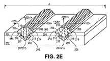
次に、図2Eにおいて、気相エピタキシャル成長(VPE)、分子線エピタキシャル成長(MBE)、又は化学気相成長(CVD)などの任意の好適なエピタキシャル成長プロセスによって、半導体基板202の上面203から、半導体材料216がエピタキシャルに成長させられる。一実施形態において、半導体材料216は、広バンドギャップ材料(例えば、2.0eVより大きいバンドギャップを持つ任意の材料)、III−V族材料、又は非固有基板上にエピタキシャル成長する間にその結晶構造中に転位欠陥及び積層欠陥に悩まされる任意の材料から構成される。1つの実施形態において、半導体材料216はGaNである。1つの特定の実施形態において、半導体材料216はGaNであり、非固有基板202はシリコンである。 Next, in FIG. 2E, the
最初に半導体材料216は、トレンチ207の限られた境界内にエピタキシャルに成長し、トレンチ材料215を形成する。従って、半導体材料216は横方向に成長することはできない。このため、半導体材料216は、トレンチ207内で実質的に鉛直に(すなわち、<0001>方向に)成長する。エピタキシャル成長中に、複数の貫通転位欠陥217が半導体材料216中に形成され得る。これらの欠陥は、半導体材料216と非固有基板202との間の格子不整合によって引き起こされる。非固有基板は、非固有基板からエピタキシャルに成長させられた半導体材料と、不整合格子構造及び/又は不整合格子定数を有する任意の基板である。複数の貫通転位欠陥217は、半導体基板202の上面203から生じ、半導体材料216の中を通って、主に鉛直方向に増殖する。水平方向及び斜め方向に増殖する複数の貫通転位欠陥は、トレンチ207の側壁209で終端させられる。このため、水平方向及び斜め方向に増殖する貫通転位欠陥が、半導体基板202の上面205の上方に継続して増殖することは非常に少ない。むしろ、鉛直に増殖する欠陥だけが、上面205の上方に継続して増殖する。複数の実施形態において、トレンチ材料215の欠陥密度は1E9cm−2より高い。Initially,
基板202の上面203の変形V溝形状は、半導体材料216のエピタキシャル成長を促進する。平坦な<100>表面形状と比較すると、V溝形状は、エピタキシャル成長中に、GaNウルツ鉱型結晶とより良好な結晶整合を可能とする向きに、上面203において、シリコン立方晶系結晶を配置する。より良好な結晶整合は、2つの結晶構造の間の格子不整合による複数の悪影響を有利に低減させる。1つの実施形態において、V溝形状は格子不整合を、平坦な<100>表面形状に成長させた場合に見られる41%から17%に減少させる。 The deformed V-groove shape of the
半導体材料216がSTI層204の上面205の上方に成長する場合、半導体材料216は横方向に(すなわち、<100>方向に)上面205の上に、横方向エピタキシャル過成長(LEO)によって成長する。横方向に成長した半導体材料206は、貫通転位欠陥217が非常に少なくなり得る。その理由は、水平方向及び斜め方向に増殖する欠陥217の大部分は、トレンチ207の側壁209ですでに終端しているからである。このため、STI層204の上面205の上に配置され横方向に成長した半導体材料206は、欠陥が著しく少ない(「欠陥のない」)実質的に高品質な材料である。1つの実施形態において、欠陥のない横方向に成長した半導体材料206の欠陥密度は、1E9cm−2より低い。代替的な一実施形態において、欠陥のない横方向に成長した半導体材料206の欠陥密度は、2E7cm−2より低い。When the
横方向に成長した半導体材料206は、そのLEOの一時点において、上面205の上に距離218だけ延在する。横方向に成長した半導体材料206がLEOを継続するにつれて、隣接する半導体材料の複数の側面219が一体化して半導体材料216及び206のブランケット層を形成するまで、複数の側面219は<100>方向に拡大し、隣接する横方向に成長した半導体材料206に向かって延在する。 The laterally grown
図2Fを参照すると、隣接する半導体材料の2つ側面219が一体化する地点に、シーム224が形成される。隣接する横方向にオーバーフローする材料からシーム224に加わる圧力は、シーム224の周りの部分222に形成された複数の欠陥をもたらす。このため、半導体材料216及び206のブランケット層は、欠陥部分221及び222と欠陥のない部分220とを含む。いくつかの実施形態において、欠陥部分221及び222の半導体材料216の欠陥密度は、1E9cm−2より高いが、欠陥のない部分220の欠陥のない半導体材料206の欠陥密度は、1E9cm−2より低い。従って、欠陥のない半導体206は、トレンチ材料215より著しく低い欠陥密度を有する。半導体材料216及び206のブランケット層を形成した後に、半導体材料216及び206のブランケット層は続いて平坦化される。必要に応じて、CMPなどの任意の好適な平坦化プロセスが、半導体材料216及び206のブランケット層を平坦化すべく実行され得る。Referring to FIG. 2F, a
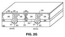
図2Gに示されるように、半導体材料216及び206のブランケット層の上に直接、絶縁層228が形成される。絶縁層228は、二酸化ケイ素などの任意の好適な誘電体から構成され得る。任意の周知の堆積技術が、絶縁層228を形成するのに使用され得る。絶縁層228は、半導体材料216及び206のブランケット層の上面を、続くプロセス条件にさらすことから分離する。 As shown in FIG. 2G, an insulating
次に、図2Hに図示されるように、部分221及び222内の半導体材料216及び206のブランケット層の欠陥部分がエッチングされて、チャネル構造206と、トレンチ材料215を含むトレンチ207とを形成する。結果として、STI層204の上面205、チャネル構造206の複数の側面211、及びトレンチ材料215の上面223が露出される。トレンチ材料215の上面223、及びチャネル構造206の複数の側面211は、続く半導体材料のエピタキシャル成長のための核形成表面を提供し得る。いくつかの実施形態において、トレンチ材料215の上面223は、図2Hに図示されるように、STI層204の上面205と実質的に同一平面上にある。しかしながら、複数の代替的実施形態において、トレンチ材料215の上面223は、STI層204の上面205と実質的に同一平面上にない。このため、トレンチ材料215の上面223は、STI層204の上面205より低くも、高くもなり得る。一実施形態において、トレンチ材料215の上面223がSTI層204の上面205より高い場合に、トレンチ材料215はチャネル構造206に直接隣接する。代替的な一実施形態において、トレンチ材料215の上面223がSTI層204の上面205より低い場合、トレンチ207は、トレンチ材料215とは異なる半導体材料を含む。例えば、GaNから構成されたトレンチ材料215は、トレンチ207からエッチングされ、その後、InGaNで充填され得る。いかなる場合でも、トレンチ207内の半導体材料は、半導体材料のエピタキシャル成長のための核形成表面を提供する。任意の好適なマスキング及びエッチングプロセスが、ブランケット層216の複数の欠陥部分を除去するのに使用され得る。1つの実施形態において、Cl2プラズマを使用するドライエッチングプロセスが、ブランケット層216及び206の欠陥部分を除去するのに使用される。Next, as illustrated in FIG. 2H, defective portions of the blanket layer of
その後、図2Iに示されるように、ソース208及びドレイン210のための半導体材料が、ブランケット層216及び206に形成された複数の開口部内にエピタキシャルに成長させられる。このため、ソース208及びドレイン210は、チャネル構造206に対して自己整合され得る。露出された、トレンチ材料215の上面223及びチャネル構造206の複数の側面211は、ソース208及びドレイン210がエピタキシャルに成長し得る核形成表面として機能を果たす。さらに、絶縁層228は、半導体材料のエピタキシャル成長が、チャネル構造206の上部に生じないようにする。このため、ソース208及びドレイン210は、チャネル構造206の両側に形成する。ドレイン210は、STI層204の上面205の上に直接配置され得て、ソース208は、ソース・イン・トレンチ構造を形成すべく、トレンチ材料215の上面223の上に直接形成され得る。トレンチ材料215の上のソース208の核形成は、トレンチ材料215を介して、ソース208を基板202と熱的に連結し得る。ソース208と基板202との間の直接の熱伝達は、直接のヒートシンクを基板202に提供し、トランジスタ動作中の熱の散逸を有利に向上させる。いくつかの実施形態において、ソース208はトレンチ材料215の上に形成するが、複数の代替的実施形態は、ソース208及びドレイン210の位置を逆にし得る。 Thereafter, as shown in FIG. 2I, semiconductor material for the
ソース208及びドレイン210は、チャネル構造206とは異なる半導体材料から構成され得る。これらの半導体材料は異なり得るが、ソース208及びドレイン210の格子構造は、エピタキシャル成長が可能であるように、チャネル構造206と類似し得る。一実施形態において、第1コンタクト(不図示)との接触抵抗を最小化すべく、ソース208及びドレイン210は、全体の有効バンドギャップがチャネル構造206より狭い半導体材料から構成され得る。本発明の一実施形態において、チャネル構造206はGaNから構成され、ソース208及びドレイン210は、InGaNなどのGaN合金から構成される。ソース208及びドレイン210は、VPE、MBE、及びCVDなどの任意の周知のエピタキシャル成長技術によって形成され得る。
一実施形態によると、ソース208及びドレイン210を形成するのに使用される、より狭いバンドギャップの半導体材料は、より導電性の高い元素の量を増大させることによって取得される。例えば、一実施形態において、ソース208及びイドレイン210のためのInGaN合金を形成すべく、InNがGaNと合金化される。InNは0.9eVのバンドギャップを有するので、InGaN合金中のInの量を増大させるにつれて、InGaNの全体の有効バンドギャップは減少する。特定の一実施形態において、Inの濃度は、InGaNの全体の有効バンドギャップが1.5eVから3.2eVに及ぶようになっている。さらに、InGaNの結晶構造は、GaNに類似している。このため、InGaN合金は、GaNを含むチャネル構造206の複数の側面211からエピタキシャルに成長するとともに、第1コンタクト(不図示)との接触抵抗を最小化するために狭いバンドギャップを維持し得る。また、ソース208及びドレイン210は、これらの全体の有効バンドギャップをさらに低減させるべく、高濃度にドープされたN+半導体材料から構成され得る。高濃度にドープされたN+半導体材料を形成すべく、シリコンなどの任意の好適なN+ドーパントが、ソース208及びドレイン210のエピタキシャル成長中に導入され得る。5E19cm−3をはるかに超える濃度にシリコンのドーパントを増大させると、ソース208及びドレイン210を形成するプロセスは、エピタキシャル成長というよりはブランケット堆積により近くなることが理解されるべきである。このため、当業者は、N+ドーパント濃度を最大化するとともに、ソース208及びドレイン210のエピタキシャル成長を維持すべく、ドーパント濃度を調整し得る。1つの実施形態において、高濃度にドープされたN+半導体材料のドーピング濃度は、5E19cm−3もの高濃度になる。代替的な一実施形態において、高濃度にドープされたN+半導体材料のドーピング濃度は、40Ω/□から50Ω/□のシート抵抗を持つ半導体材料をもたらす。According to one embodiment, the narrower bandgap semiconductor material used to form the
チャネル構造206と異なり、ソース208及びドレイン210は、単に電流フローのノードとして働くに過ぎない。このため、ソース208及びドレイン210は、チャネル構造206と同じ程度の低欠陥密度を必要としなくてもよい。複数の実施形態において、ソース208及びドレイン210は、1E9cm−2より高い欠陥密度を有する。Unlike
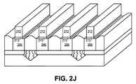
次に、図2Jに示されるように、ゲート誘電体213及びゲート電極212を含むゲートスタックが、チャネル構造206の上に形成される。二酸化ケイ素などの任意の好適な材料が、ゲート誘電体213を形成するのに使用され得る。一実施形態において、絶縁層228が、ゲート誘電体213として使用される。複数の代替的実施形態において、誘電体層228は除去されて、ゲート誘電体213が形成される。ゲート電極212は、ポリシリコンなどの任意の好適な材料から構成される。ゲート電極212及びゲート誘電体213は、当分野において周知の任意の堆積及びエッチング技術によって形成され得る。 Next, as shown in FIG. 2J, a gate stack including the
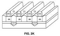
その後、図2Kにおいて、複数のゲートスペーサ214が、ゲートスタック212及び213の両側に形成され得る。複数のゲートスペーサ214は、二酸化ケイ素、窒化ケイ素、又は炭化ケイ素などの任意の好適なスペーサ材料から構成され得る。さらに、任意の好適なスペーサエッチングプロセスが、ゲートスペーサ214を形成するのに使用され得る。 Thereafter, in FIG. 2K, a plurality of
図3は、本発明の1つの実施例を用いて実装されたコンピューティングシステム300を示す。コンピューティングデバイス300は、ボード302を収容する。ボード302は、限定されないが、プロセッサ304及び少なくとも1つの通信チップ306を含む、複数の構成要素を含んでよい。プロセッサ304は、ボード302に物理的且つ電気的に連結される。いくつかの実施例において、少なくとも1つの通信チップ306も、ボード302に物理的且つ電気的に連結される。さらなる複数の実施例において、通信チップ306はプロセッサ304の一部である。 FIG. 3 illustrates a computing system 300 implemented using one embodiment of the present invention. Computing device 300
その複数の用途に応じて、コンピューティングデバイス300は、ボード302に物理的且つ電気的に連結されても、されなくてもよい他の複数の構成要素を含んでよい。これらの他の構成要素は、限定されないが、揮発性メモリ(例えば、DRAM)、不揮発性メモリ(例えば、ROM)、フラッシュメモリ、グラフィックプロセッサ、デジタル信号プロセッサ、暗号プロセッサ、チップセット、アンテナ、ディスプレイ、タッチスクリーンディスプレイ、タッチスクリーンコントローラ、バッテリ、オーディオコーデック、ビデオコーデック、電力増幅器、全地球測位システム(GPS)デバイス、コンパス、加速度計、ジャイロスコープ、スピーカ、カメラ、及び大容量記憶デバイス(ハードディスクドライブ、コンパクトディスク(CD)、デジタル多目的ディスク(DVD)等)を含む。 Depending on its multiple applications, computing device 300 may include other multiple components that may or may not be physically and electrically coupled to
通信チップ306は、コンピューティングデバイス300との間でデータを伝送するための無線通信を可能にする。「無線」という用語及びその複数の派生語は、非固体媒体を介し、変調電磁放射線を使用することによって、データ通信を行い得る複数の回路、複数のデバイス、複数のシステム、複数の方法、複数の技術、複数の通信、複数のチャネルなどを説明するのに使用されてもよい。この用語は、複数の関連デバイスは何ら有線を含ないことを暗示してはいないが、いくつかの実施形態においては、含まないかもしれない。通信チップ306は、限定されないが、Wi−Fi(IEEE802.11ファミリー)、WiMAX(IEEE802.16ファミリー)、IEEE802.20、ロングタームエボリューション(LTE)、Ev−DO、HSPA+、HSDPA+、HSUPA+、EDGE、GSM(登録商標)、GPRS、CDMA、TDMA、DECT、Bluetooth(登録商標)、それらの派生物、並びに、3G、4G、5G及び以降に指定された任意の他の無線プロトコルを含む、複数の無線規格又は無線プロトコルのいずれかを実装してよい。コンピューティングデバイス300は、複数の通信チップ306を含んでよい。例えば、第1通信チップ306は、Wi−Fi(登録商標)及びBluetooth(登録商標)などの複数の近距離無線通信に専用化されてよく、第2通信チップ306は、GPS、EDGE、GPRS、CDMA、WiMAX(登録商標)、LTE、Ev−DO及びその他などの複数の長距離無線通信に専用化されてもよい。 The
コンピューティングデバイス300のプロセッサ304は、プロセッサ304内にパッケージ化された集積回路ダイを含む。本発明のいくつかの実施例において、プロセッサの集積回路ダイは、本発明の複数の実施例に従って形成される、非固有半導体基板上に形成された複数の広バンドギャップトランジスタなどの1又は複数のデバイスを含む。「プロセッサ」という用語は、複数のレジスタ及び/又はメモリからの電子データを処理して、その電子データを複数のレジスタ及び/又はメモリに格納され得る他の電子データに変換する、任意のデバイス又はデバイスの一部を指してもよい。 The
通信チップ306は、通信チップ306内にパッケージ化された集積回路ダイも含む。本発明の別の実施例に従うと、通信チップの集積回路ダイは、複数のフード層を伴った複数のエアギャップ相互接続など、本発明の複数の実施例に従って形成される1又は複数のデバイスを含む。
さらなる複数の実施例において、コンピューティングデバイス300内に収納された別の構成要素は、複数のフード層を伴った複数のエアギャップ相互接続など、本発明の複数の実施例に従って形成される1又は複数のデバイスを含む集積回路ダイを含んでよい。 In further embodiments, another component housed within computing device 300 is formed according to embodiments of the present invention, such as a plurality of air gap interconnects with a plurality of hood layers. An integrated circuit die including a plurality of devices may be included.
様々な実施例において、コンピューティングデバイス300は、ラップトップ、ネットブック、ノートブック、ウルトラブック、スマートフォン、タブレット、携帯情報端末(PDA)、ウルトラモバイルPC、携帯電話、デスクトップコンピュータ、サーバ、プリンタ、スキャナ、モニタ、セットトップボックス、エンターテイメントコントロールユニット、デジタルカメラ、携帯音楽プレイヤ、又はデジタルビデオレコーダであってよい。さらなる複数の実施例において、コンピューティングデバイス300は、データを処理する任意の他の電子デバイスであってよい。 In various embodiments, the computing device 300 can be a laptop, netbook, notebook, ultrabook, smartphone, tablet, personal digital assistant (PDA), ultra mobile PC, mobile phone, desktop computer, server, printer, scanner. , Monitors, set-top boxes, entertainment control units, digital cameras, portable music players, or digital video recorders. In further embodiments, computing device 300 may be any other electronic device that processes data.
一実施形態において、半導体トランジスタ構造は、半導体基板と、シリコン基板の上に形成された絶縁層と、絶縁層を貫いてシリコン基板内に延在するトレンチであって、第1のIII−V族半導体材料を含むトレンチ材料を含むトレンチと、絶縁層の上に直接、トレンチと隣接して形成されたチャネル構造であって、トレンチ材料の欠陥密度より低い欠陥密度を有する第2のIII−V族半導体材料を含むチャネル材料で形成される、チャネル構造と、チャネル構造の両側に形成されたソース及びドレインであって、ソースはトレンチ材料の上に形成される、ソース及びドレインと、チャネル構造の上方に形成されたゲート電極と、を備える。別の実施形態において、トレンチ材料及びチャネル材料は、窒化ガリウムを含む。さらに別の実施形態において、チャネル材料は、1E9cm−2より低い欠陥密度を有する。代替的な一実施形態において、トレンチ材料は、1E9cm−2より高い欠陥密度を有する。別の実施形態において、ソースはトレンチ材料の上に形成され、ドレインは絶縁層の上に形成される。さらに別の実施形態において、ソースは、トレンチ材料と熱的に連結される。代替的な一実施形態において、ソースは、シリコン基板と熱的に連結される。1つの実施形態において、ソース及びドレインは、窒化インジウムガリウムを含む。1つの他の実施形態において、窒化インジウムガリウムは、5E19cm−3より高いN+ドーピング濃度を有する。さらに別の実施形態において、半導体基板はシリコンを含み、トレンチ材料及びチャネル構造はGaNを含み、ソース及びドレインはInGaNを含む。In one embodiment, the semiconductor transistor structure includes a semiconductor substrate, an insulating layer formed on the silicon substrate, and a trench extending through the insulating layer into the silicon substrate, the first III-V group. A trench comprising a trench material comprising a semiconductor material, and a second III-V group having a defect density lower than the defect density of the trench material, wherein the channel structure is formed directly on the insulating layer and adjacent to the trench. A channel structure formed of a channel material including a semiconductor material, and a source and a drain formed on both sides of the channel structure, the source formed on the trench material, and above the channel structure And a gate electrode formed on the substrate. In another embodiment, the trench material and channel material comprise gallium nitride. In yet another embodiment, the channel material has a defect density lower than 1E9 cm−2 . In an alternative embodiment, the trench material has a defect density higher than 1E9 cm−2 . In another embodiment, the source is formed on the trench material and the drain is formed on the insulating layer. In yet another embodiment, the source is thermally coupled to the trench material. In an alternative embodiment, the source is thermally coupled to the silicon substrate. In one embodiment, the source and drain include indium gallium nitride. In one other embodiment, the indium gallium nitride has an N+ doping concentration greater than 5E19 cm−3 . In yet another embodiment, the semiconductor substrate comprises silicon, the trench material and channel structure comprise GaN, and the source and drain comprise InGaN.
1つの実施形態において、半導体トランジスタ構造を形成する方法は、半導体基板上にパターニングされた絶縁層を形成する段階であって、パターニングされた絶縁層は半導体基板の被覆されていない部分を露出させる、形成する段階と、半導体基板の被覆されていない部分において、半導体基板にトレンチを形成する段階と、半導体材料がパターニングされた絶縁層上に横方向にオーバーフローして、ブランケット層を形成するように、トレンチ内に半導体材料を成長させる段階であって、半導体材料はIII−V族半導体材料を含む、成長させる段階と、チャネル構造及びトレンチ材料が残るように、ブランケット層の一部分をエッチング除去する段階であって、チャネル構造は、トレンチ材料より低欠陥密度を有する、エッチング除去する段階と、チャネル構造の両側にソース及びドレインを形成する段階と、チャネル構造の上にゲート電極を形成する段階と、を備える。代替的な一実施形態において、隣接した横方向にオーバーフローする材料と一体化させられた材料によって、ブランケット層が形成される。別の実施形態において、半導体基板にトレンチを形成する段階は、半導体基板の被覆されていない部分の選択エッチングである。さらに別の実施形態では、III−V族半導体材料を含む材料は、窒化ガリウムである。1つの実施形態において、ブランケット層の一部は、チャネル構造の欠陥密度より高い欠陥密度を有する欠陥部分である。1つの他の実施形態において、欠陥部分は、1E9cm−2より高い欠陥密度を含む。代替的な一実施形態において、チャネル構造の欠陥密度は、1E9cm−2より低い。別の実施形態において、トレンチ材料は、1E9cm−2より高い欠陥密度を有する。さらに別の実施形態において、ソース及びドレインは、エピタキシャル成長によって形成される。1つの実施形態において、エピタキシャル成長は、窒化インジウムガリウム構造を形成する。1つの他の実施形態において、窒化インジウムガリウム構造は、5E19cm−3より高いN+ドーピング濃度で形成される。In one embodiment, a method of forming a semiconductor transistor structure includes forming a patterned insulating layer on a semiconductor substrate, the patterned insulating layer exposing an uncovered portion of the semiconductor substrate. Forming a trench in the semiconductor substrate in an uncovered portion of the semiconductor substrate; and overflowing the semiconductor material laterally over the patterned insulating layer to form a blanket layer. Growing a semiconductor material in the trench, the semiconductor material comprising a III-V semiconductor material, and etching away a portion of the blanket layer so that the channel structure and the trench material remain. The channel structure has a lower defect density than the trench material, etched away Comprising the steps that, forming a source and a drain on both sides of the channel structure, and forming a gate electrode on the channel structure. In an alternative embodiment, the blanket layer is formed by a material that is integrated with an adjacent lateral overflow material. In another embodiment, forming the trench in the semiconductor substrate is a selective etch of an uncovered portion of the semiconductor substrate. In yet another embodiment, the material comprising a III-V semiconductor material is gallium nitride. In one embodiment, a portion of the blanket layer is a defect portion having a defect density that is higher than the defect density of the channel structure. In one other embodiment, the defect portion comprises a defect density greater than 1E9 cm−2 . In an alternative embodiment, the defect density of the channel structure is lower than 1E9 cm−2 . In another embodiment, the trench material has a defect density greater than 1E9 cm−2 . In yet another embodiment, the source and drain are formed by epitaxial growth. In one embodiment, the epitaxial growth forms an indium gallium nitride structure. In one other embodiment, the indium gallium nitride structure is formed with an N+ doping concentration greater than 5E19 cm−3 .
一実施形態において、システムオンチップは、半導体基板と、半導体基板上に形成された金属酸化物半導体トランジスタと、半導体基板上に金属酸化物半導体トランジスタと隣接して形成された広バンドギャップ半導体トランジスタと、を備え、広バンドギャップ半導体トランジスタは、半導体基板の上に形成された絶縁層と、絶縁層を貫いて形成され、半導体基板内に延在するトレンチであって、III−V族半導体材料を含むトレンチ材料で充填される、トレンチと、絶縁層の上に直接、トレンチと隣接して形成されたチャネル構造であって、トレンチ材料の欠陥密度より低い欠陥密度を有するIII−V族半導体材料を含むチャネル材料で形成される、チャネル構造と、チャネル構造の両側に形成されたソース及びドレインと、チャネル構造の上に形成されたゲート電極と、を有する。代替的な一実施形態において、トレンチ材料及びチャネル材料は、窒化ガリウムを含む。別の実施形態において、チャネル材料は、1E9cm−2より低い欠陥密度を有する。さらに別の実施形態において、トレンチ材料は、1E9cm−2より高い欠陥密度を有する。1つの実施形態において、ソースはトレンチ材料の上に形成され、ドレインは絶縁層の上に形成される。1つの他の実施形態において、ソースは、トレンチ材料と熱的に連結される。異なる一実施形態において、ソースは、半導体基板と熱的に連結される。別の実施形態において、ソース及びドレインは窒化インジウムガリウムを含む。さらに別の実施形態において、窒化インジウムガリウムは、5E19cm−3より高いN+ドーピング濃度を有する。In one embodiment, a system-on-chip includes a semiconductor substrate, a metal oxide semiconductor transistor formed on the semiconductor substrate, and a wide band gap semiconductor transistor formed on the semiconductor substrate adjacent to the metal oxide semiconductor transistor. The wide band gap semiconductor transistor includes an insulating layer formed on the semiconductor substrate, and a trench formed through the insulating layer and extending into the semiconductor substrate. A trench filled with a trench material and a channel structure formed directly on the insulating layer adjacent to the trench and having a defect density lower than that of the trench material. A channel structure formed of a channel material including the source and drain formed on both sides of the channel structure; And a gate electrode formed over the structure. In an alternative embodiment, the trench material and the channel material comprise gallium nitride. In another embodiment, the channel material has a defect density less than 1E9 cm−2 . In yet another embodiment, the trench material has a defect density greater than 1E9 cm−2 . In one embodiment, the source is formed on the trench material and the drain is formed on the insulating layer. In one other embodiment, the source is thermally coupled to the trench material. In a different embodiment, the source is thermally coupled to the semiconductor substrate. In another embodiment, the source and drain comprise indium gallium nitride. In yet another embodiment, the indium gallium nitride has an N+ doping concentration greater than 5E19 cm−3 .
本発明の様々な態様を利用する際に、上記の複数の実施形態の複数の組み合わせ又は複数の変形が、非固有半導体基板上に広バンドギャップトランジスタを形成するために可能であることが、当業者には明らかになるであろう。本発明の複数の実施形態は、複数の構造的特徴及び/又は複数の方法論的作用に特有の言語で説明されたが、添付された特許請求の範囲で定められた本発明は、説明された複数の具体的な特徴又は作用に必ずしも限定されないことが理解されるべきである。むしろ、開示された複数の具体的な特徴及び作用は、本発明の複数の実施形態を例示するのに有用な、特許請求された発明の特に適切な複数の実施例と理解されるべきである。 In utilizing the various aspects of the present invention, it will be appreciated that combinations or variations of the above embodiments are possible to form a wide bandgap transistor on a non-unique semiconductor substrate. It will be clear to the contractor. While embodiments of the present invention have been described in language specific to a plurality of structural features and / or a plurality of methodological actions, the invention as defined in the appended claims has been described. It should be understood that the invention is not necessarily limited to a plurality of specific features or actions. Rather, the specific features and acts disclosed are to be understood as particularly suitable examples of the claimed invention that are useful in illustrating the embodiments of the present invention. .
Claims (25)
Translated fromJapanese前記半導体基板の上に形成された絶縁層と、
前記絶縁層を貫いて前記半導体基板内に延在するトレンチであって、前記トレンチは第1のIII−V族半導体材料を含むトレンチ材料を含むトレンチと、
前記絶縁層の上に直接、前記トレンチと隣接して形成されたチャネル構造であって、前記チャネル構造は、前記トレンチ材料の欠陥密度より低い欠陥密度を有する第2のIII−V族半導体材料を含むチャネル材料で形成される、チャネル構造と、
前記チャネル構造の両側に形成されたソース及びドレインであって、前記ソースは、前記トレンチ材料の上に形成される、ソース及びドレインと、
前記チャネル構造の上方に形成されたゲート電極と、
を備える、
半導体トランジスタ構造。A semiconductor substrate;
An insulating layer formed on the semiconductor substrate;
A trench extending through the insulating layer into the semiconductor substrate, the trench comprising a trench material comprising a first III-V semiconductor material;
A channel structure formed directly on the insulating layer and adjacent to the trench, the channel structure comprising a second group III-V semiconductor material having a defect density lower than that of the trench material. A channel structure formed of a channel material comprising:
A source and a drain formed on both sides of the channel structure, the source formed on the trench material; and
A gate electrode formed above the channel structure;
Comprising
Semiconductor transistor structure.
請求項1に記載の半導体トランジスタ構造。The trench material and the channel material include gallium nitride,
The semiconductor transistor structure according to claim 1.
請求項1又2に記載の半導体トランジスタ構造。The channel material has a defect density lower than 1E9 cm−2 ;
3. The semiconductor transistor structure according to claim 1 or 2.
請求項1から3の何れか一項に記載の半導体トランジスタ構造。The trench material has a defect density higher than 1E9 cm−2 ;
The semiconductor transistor structure according to claim 1.
請求項1から4の何れか一項に記載の半導体トランジスタ構造。The source is formed on the trench material and the drain is formed on the insulating layer;
The semiconductor transistor structure according to claim 1.
請求項5に記載の半導体トランジスタ構造。The source is thermally coupled to the semiconductor substrate;
The semiconductor transistor structure according to claim 5.
請求項1から6の何れか一項に記載の半導体トランジスタ構造。The source and the drain include indium gallium nitride,
The semiconductor transistor structure according to claim 1.
請求項7に記載の半導体トランジスタ構造。The indium gallium nitride has an N+ doping concentration higher than 5E19 cm−3 ;
The semiconductor transistor structure according to claim 7.
請求項1から8の何れか一項に記載の半導体トランジスタ構造。The semiconductor substrate comprises silicon; the trench material and the channel structure comprise GaN; and the source and drain comprise InGaN.
The semiconductor transistor structure according to claim 1.
前記半導体基板の被覆されていない前記部分において、前記半導体基板にトレンチを形成する段階と、
半導体材料がパターニングされた前記絶縁層上に横方向にオーバーフローして、ブランケット層を形成するように、前記トレンチ内に前記半導体材料を成長させる段階であって、前記半導体材料はIII−V族半導体材料を含む、成長させる段階と、
チャネル構造及びトレンチ材料が残るように、前記ブランケット層の一部分をエッチング除去する段階であって、前記チャネル構造は、前記トレンチ材料より低欠陥密度を有する、エッチング除去する段階と、
前記チャネル構造の両側にソース及びドレインを形成する段階と、
前記チャネル構造の上にゲート電極を形成する段階と、
を備える、
半導体トランジスタ構造形成方法。Forming a patterned insulating layer on a semiconductor substrate, wherein the patterned insulating layer exposes an uncovered portion of the semiconductor substrate; and
Forming a trench in the semiconductor substrate in the uncovered portion of the semiconductor substrate;
Growing the semiconductor material in the trench such that the semiconductor material overflows laterally on the patterned insulating layer to form a blanket layer, the semiconductor material being a III-V semiconductor Including growing material, and
Etching away a portion of the blanket layer to leave a channel structure and trench material, the channel structure having a lower defect density than the trench material;
Forming a source and a drain on both sides of the channel structure;
Forming a gate electrode on the channel structure;
Comprising
Semiconductor transistor structure forming method.
請求項10に記載の半導体トランジスタ構造形成方法。The blanket layer is formed by the semiconductor material that is integrated with an adjacent lateral overflow material.
The method for forming a semiconductor transistor structure according to claim 10.
請求項10又は11に記載の半導体トランジスタ構造形成方法。The step of forming a trench in the semiconductor substrate is a selective etching of the uncovered portion of the semiconductor substrate;
12. The method for forming a semiconductor transistor structure according to claim 10 or 11.
請求項10から12の何れか一項に記載の半導体トランジスタ構造形成方法。The semiconductor material comprising a III-V semiconductor material is gallium nitride;
The method for forming a semiconductor transistor structure according to claim 10.
請求項10から13の何れか一項に記載の半導体トランジスタ構造形成方法。The portion of the blanket layer is a defect portion having a defect density higher than the defect density of the channel structure;
The method for forming a semiconductor transistor structure according to claim 10.
請求項14に記載の半導体トランジスタ構造形成方法。The defect portion includes a defect density higher than 1E9 cm−2 ;
The method for forming a semiconductor transistor structure according to claim 14.
請求項14に記載の半導体トランジスタ構造形成方法。The defect density of the channel structure is lower than 1E9 cm−2 ;
The method for forming a semiconductor transistor structure according to claim 14.
請求項10から16の何れか一項に記載の半導体トランジスタ構造形成方法。The source and the drain are formed by epitaxial growth.
The method for forming a semiconductor transistor structure according to claim 10.
請求項17に記載の半導体トランジスタ構造形成方法。The epitaxial growth forms an indium gallium nitride structure;
The method for forming a semiconductor transistor structure according to claim 17.
前記半導体基板上に形成された金属酸化物半導体トランジスタと、
前記半導体基板上に前記金属酸化物半導体トランジスタと隣接して形成された広バンドギャップ半導体トランジスタと、
を備え、
前記広バンドギャップ半導体トランジスタは、
前記半導体基板の上に形成された絶縁層と、
前記絶縁層を貫いて形成され、前記半導体基板内に延在するトレンチであって、前記トレンチは、III−V族半導体材料を含むトレンチ材料で充填される、トレンチと、
前記絶縁層の上に直接、前記トレンチと隣接して形成されたチャネル構造であって、前記チャネル構造は、前記トレンチ材料の欠陥密度より低い欠陥密度を有するIII−V族半導体材料を含むチャネル材料で形成される、チャネル構造と、
前記チャネル構造の両側に形成されたソース及びドレインと、
前記チャネル構造の上に形成されたゲート電極と、
を有する、
システムオンチップ。A semiconductor substrate;
A metal oxide semiconductor transistor formed on the semiconductor substrate;
A wide band gap semiconductor transistor formed adjacent to the metal oxide semiconductor transistor on the semiconductor substrate;
With
The wide band gap semiconductor transistor is:
An insulating layer formed on the semiconductor substrate;
A trench formed through the insulating layer and extending into the semiconductor substrate, the trench being filled with a trench material comprising a III-V semiconductor material;
A channel structure formed directly on the insulating layer and adjacent to the trench, the channel structure comprising a III-V semiconductor material having a defect density lower than that of the trench material A channel structure formed by:
A source and a drain formed on both sides of the channel structure;
A gate electrode formed on the channel structure;
Having
System on chip.
請求項19に記載のシステムオンチップ。The trench material and the channel material include gallium nitride,
20. The system on chip according to claim 19.
請求項19又は20に記載のシステムオンチップ。The channel material has a defect density lower than 1E9 cm−2 ;
The system on chip according to claim 19 or 20.
請求項19から21の何れか一項に記載のシステムオンチップ。The trench material has a defect density higher than 1E9 cm−2 ;
The system-on-chip according to any one of claims 19 to 21.
請求項19から22の何れか一項に記載のシステムオンチップ。The source is formed on the trench material and the drain is formed on the insulating layer;
System-on-chip according to any one of claims 19 to 22.
請求項19から23の何れか一項に記載のシステムオンチップ。The source is thermally coupled to the semiconductor substrate;
The system on chip according to any one of claims 19 to 23.
請求項19から24の何れか一項に記載のシステムオンチップ。The source and the drain include indium gallium nitride,
The system on chip according to any one of claims 19 to 24.
Applications Claiming Priority (1)
| Application Number | Priority Date | Filing Date | Title |
|---|---|---|---|
| PCT/US2013/077621WO2015099688A1 (en) | 2013-12-23 | 2013-12-23 | Wide band gap transistors on non-native semiconductor substrates and methods of manufacture thereof |
Publications (2)
| Publication Number | Publication Date |
|---|---|
| JP2017501562Atrue JP2017501562A (en) | 2017-01-12 |
| JP6315852B2 JP6315852B2 (en) | 2018-04-25 |
Family
ID=53479359
Family Applications (1)
| Application Number | Title | Priority Date | Filing Date |
|---|---|---|---|
| JP2016527361AActiveJP6315852B2 (en) | 2013-12-23 | 2013-12-23 | Semiconductor transistor structure, system-on-chip, and semiconductor transistor structure forming method |
Country Status (7)
| Country | Link |
|---|---|
| US (1) | US9660085B2 (en) |
| EP (1) | EP3087612A4 (en) |
| JP (1) | JP6315852B2 (en) |
| KR (1) | KR102167518B1 (en) |
| CN (1) | CN105745759B (en) |
| TW (1) | TWI565054B (en) |
| WO (1) | WO2015099688A1 (en) |
Cited By (4)
| Publication number | Priority date | Publication date | Assignee | Title |
|---|---|---|---|---|
| KR20200036707A (en)* | 2018-09-27 | 2020-04-07 | 타이완 세미콘덕터 매뉴팩쳐링 컴퍼니 리미티드 | Fin-based field effect transistors |
| JPWO2020245695A1 (en)* | 2019-06-07 | 2020-12-10 | ||
| US11257818B2 (en) | 2018-09-27 | 2022-02-22 | Taiwan Semiconductor Manufacturing Co., Ltd. | Fin-based field effect transistors |
| JP2023548938A (en)* | 2020-11-13 | 2023-11-21 | インターナショナル・ビジネス・マシーンズ・コーポレーション | A fin stack comprising a tensile strained fin section and a compressively strained fin section. |
Families Citing this family (13)
| Publication number | Priority date | Publication date | Assignee | Title |
|---|---|---|---|---|
| DE102013103602A1 (en)* | 2013-04-10 | 2014-10-16 | Osram Opto Semiconductors Gmbh | Optoelectronic semiconductor chip and method for its production |
| US9478708B2 (en) | 2015-03-11 | 2016-10-25 | International Business Machines Corporation | Embedded gallium—nitride in silicon |
| EP3353813B1 (en) | 2015-09-25 | 2024-06-05 | Intel Corporation | Semiconductor device contacts with increased contact area |
| US9570300B1 (en)* | 2016-02-08 | 2017-02-14 | International Business Machines Corporation | Strain relaxed buffer layers with virtually defect free regions |
| WO2017146676A1 (en)* | 2016-02-22 | 2017-08-31 | Intel Corporation | Apparatus and methods to create an active channel having indium rich side and bottom surfaces |
| US9793113B2 (en)* | 2016-03-21 | 2017-10-17 | Globalfoundries Inc. | Semiconductor structure having insulator pillars and semiconductor material on substrate |
| GB2556899B (en)* | 2016-11-24 | 2020-09-16 | Cambridge Entpr Ltd | A gallium nitride transistor |
| JP7147416B2 (en)* | 2018-09-26 | 2022-10-05 | 信越半導体株式会社 | Epitaxial wafer manufacturing method, silicon-based substrate for epitaxial growth, and epitaxial wafer |
| FR3102005B1 (en)* | 2019-10-15 | 2022-04-22 | Commissariat Energie Atomique | Method of hetero-integration of a semiconductor material of interest on a silicon substrate |
| TWI715311B (en)* | 2019-11-26 | 2021-01-01 | 國立交通大學 | Si-mosfet with wide bandgap iii-v drain and method of manufacturing the same |
| DE102020112203B4 (en) | 2020-03-13 | 2024-08-08 | Taiwan Semiconductor Manufacturing Co. Ltd. | INTEGRATED CIRCUIT AND METHOD FOR EMBEDDED PLANAR FETS WITH FINFETS |
| US11355493B2 (en)* | 2020-03-13 | 2022-06-07 | Taiwan Semiconductor Manufacturing Company, Ltd. | Method to embed planar FETs with finFETs |
| CN111816704A (en)* | 2020-08-18 | 2020-10-23 | 松山湖材料实验室 | A kind of nano switch device and preparation method thereof |
Citations (17)
| Publication number | Priority date | Publication date | Assignee | Title |
|---|---|---|---|---|
| JPH0878692A (en)* | 1994-09-01 | 1996-03-22 | Nec Corp | SOI type semiconductor device and manufacturing method thereof |
| JP2001230410A (en)* | 2000-02-18 | 2001-08-24 | Furukawa Electric Co Ltd:The | GaN-based field effect transistor and method of manufacturing the same |
| JP2004055943A (en)* | 2002-07-23 | 2004-02-19 | Matsushita Electric Ind Co Ltd | Semiconductor device and manufacturing method thereof |
| JP2006173241A (en)* | 2004-12-14 | 2006-06-29 | Matsushita Electric Ind Co Ltd | Field effect transistor and manufacturing method thereof |
| JP2006216671A (en)* | 2005-02-02 | 2006-08-17 | Toshiba Corp | Nitrogen compound semiconductor device |
| US20070281446A1 (en)* | 2006-05-31 | 2007-12-06 | Winstead Brian A | Dual surface SOI by lateral epitaxial overgrowth |
| JP2008159691A (en)* | 2006-12-21 | 2008-07-10 | Rohm Co Ltd | Nitride semiconductor element, nitride semiconductor crystal growth substrate, and method for manufacturing same |
| WO2008099901A1 (en)* | 2007-02-16 | 2008-08-21 | Sumitomo Chemical Company, Limited | Gallium nitride epitaxial crystal, method for production thereof, and field effect transistor |
| JP2008546181A (en)* | 2005-05-17 | 2008-12-18 | アンバーウェーブ システムズ コーポレイション | Lattice-mismatched semiconductor structure with low dislocation defect density and related device manufacturing method |
| JP2009016655A (en)* | 2007-07-06 | 2009-01-22 | Sanken Electric Co Ltd | Field effect semiconductor device and manufacturing method thereof |
| JP2010114112A (en)* | 2008-11-04 | 2010-05-20 | Canon Inc | Method of forming gallium nitride-based compound semiconductor layer, transfer method of gallium nitride-based compound semiconductor layer, and silicon substrate to which gallium nitride-based compound semiconductor is bonded |
| JP2010226081A (en)* | 2008-10-02 | 2010-10-07 | Sumitomo Chemical Co Ltd | Semiconductor substrate, electronic device, and method for manufacturing semiconductor substrate |
| JP2011082526A (en)* | 2009-10-08 | 2011-04-21 | Taiwan Semiconductor Manufacturing Co Ltd | Method of growing group iii-v layer on silicon using nano-scale orientation pattern |
| JP2011159795A (en)* | 2010-02-01 | 2011-08-18 | Nippon Telegr & Teleph Corp <Ntt> | Semiconductor device and method of fabricating the same |
| US20120305992A1 (en)* | 2011-06-06 | 2012-12-06 | Fabio Alessio Marino | Hybrid monolithic integration |
| JP2013045829A (en)* | 2011-08-23 | 2013-03-04 | Seiko Epson Corp | Semiconductor device, electrooptic device, power conversion apparatus and electronic apparatus |
| JP2013098559A (en)* | 2011-10-31 | 2013-05-20 | Samsung Electronics Co Ltd | Semiconductor element including iii-v compound semiconductor layer and manufacturing method of the same |
Family Cites Families (13)
| Publication number | Priority date | Publication date | Assignee | Title |
|---|---|---|---|---|
| FR2842832B1 (en) | 2002-07-24 | 2006-01-20 | Lumilog | METHOD FOR REALIZING VAPOR EPITAXY OF A GALLIUM NITRIDE FILM WITH LOW FAULT DENSITY |
| US20070090456A1 (en) | 2005-08-29 | 2007-04-26 | Jin-Yuan Lee | Soi device and method for fabricating the same |
| US7566913B2 (en)* | 2005-12-02 | 2009-07-28 | Nitronex Corporation | Gallium nitride material devices including conductive regions and methods associated with the same |
| US7687364B2 (en) | 2006-08-07 | 2010-03-30 | Intel Corporation | Low-k isolation spacers for conductive regions |
| WO2009110207A1 (en) | 2008-03-01 | 2009-09-11 | 住友化学株式会社 | Semiconductor substrate, semiconductor substrate manufacturing method, and electronic device |
| US8030666B2 (en)* | 2008-04-16 | 2011-10-04 | Taiwan Semiconductor Manufacturing Company, Ltd. | Group-III nitride epitaxial layer on silicon substrate |
| US9112085B2 (en)* | 2009-11-30 | 2015-08-18 | The Royal Institution For The Advancement Of Learning/Mcgill University | High efficiency broadband semiconductor nanowire devices |
| US8278179B2 (en) | 2010-03-09 | 2012-10-02 | Taiwan Semiconductor Manufacturing Co., Ltd. | LDD epitaxy for FinFETs |
| US8592292B2 (en)* | 2010-09-02 | 2013-11-26 | National Semiconductor Corporation | Growth of multi-layer group III-nitride buffers on large-area silicon substrates and other substrates |
| US8772831B2 (en)* | 2011-11-07 | 2014-07-08 | Taiwan Semiconductor Manufacturing Company, Ltd. | III-nitride growth method on silicon substrate |
| US8629038B2 (en)* | 2012-01-05 | 2014-01-14 | Taiwan Semiconductor Manufacturing Company, Ltd. | FinFETs with vertical fins and methods for forming the same |
| US9105571B2 (en) | 2012-02-08 | 2015-08-11 | International Business Machines Corporation | Interface engineering to optimize metal-III-V contacts |
| US20130299895A1 (en)* | 2012-05-09 | 2013-11-14 | Taiwan Semiconductor Manufacturing Co., Ltd. | Iii-v compound semiconductor device having dopant layer and method of making the same |
- 2013
- 2013-12-23JPJP2016527361Apatent/JP6315852B2/enactiveActive
- 2013-12-23EPEP13900386.7Apatent/EP3087612A4/ennot_activeWithdrawn
- 2013-12-23KRKR1020167013258Apatent/KR102167518B1/ennot_activeExpired - Fee Related
- 2013-12-23CNCN201380081129.3Apatent/CN105745759B/enactiveActive
- 2013-12-23WOPCT/US2013/077621patent/WO2015099688A1/enactiveApplication Filing
- 2013-12-23USUS15/036,780patent/US9660085B2/ennot_activeExpired - Fee Related
- 2014
- 2014-11-21TWTW103140477Apatent/TWI565054B/enactive
Patent Citations (17)
| Publication number | Priority date | Publication date | Assignee | Title |
|---|---|---|---|---|
| JPH0878692A (en)* | 1994-09-01 | 1996-03-22 | Nec Corp | SOI type semiconductor device and manufacturing method thereof |
| JP2001230410A (en)* | 2000-02-18 | 2001-08-24 | Furukawa Electric Co Ltd:The | GaN-based field effect transistor and method of manufacturing the same |
| JP2004055943A (en)* | 2002-07-23 | 2004-02-19 | Matsushita Electric Ind Co Ltd | Semiconductor device and manufacturing method thereof |
| JP2006173241A (en)* | 2004-12-14 | 2006-06-29 | Matsushita Electric Ind Co Ltd | Field effect transistor and manufacturing method thereof |
| JP2006216671A (en)* | 2005-02-02 | 2006-08-17 | Toshiba Corp | Nitrogen compound semiconductor device |
| JP2008546181A (en)* | 2005-05-17 | 2008-12-18 | アンバーウェーブ システムズ コーポレイション | Lattice-mismatched semiconductor structure with low dislocation defect density and related device manufacturing method |
| US20070281446A1 (en)* | 2006-05-31 | 2007-12-06 | Winstead Brian A | Dual surface SOI by lateral epitaxial overgrowth |
| JP2008159691A (en)* | 2006-12-21 | 2008-07-10 | Rohm Co Ltd | Nitride semiconductor element, nitride semiconductor crystal growth substrate, and method for manufacturing same |
| WO2008099901A1 (en)* | 2007-02-16 | 2008-08-21 | Sumitomo Chemical Company, Limited | Gallium nitride epitaxial crystal, method for production thereof, and field effect transistor |
| JP2009016655A (en)* | 2007-07-06 | 2009-01-22 | Sanken Electric Co Ltd | Field effect semiconductor device and manufacturing method thereof |
| JP2010226081A (en)* | 2008-10-02 | 2010-10-07 | Sumitomo Chemical Co Ltd | Semiconductor substrate, electronic device, and method for manufacturing semiconductor substrate |
| JP2010114112A (en)* | 2008-11-04 | 2010-05-20 | Canon Inc | Method of forming gallium nitride-based compound semiconductor layer, transfer method of gallium nitride-based compound semiconductor layer, and silicon substrate to which gallium nitride-based compound semiconductor is bonded |
| JP2011082526A (en)* | 2009-10-08 | 2011-04-21 | Taiwan Semiconductor Manufacturing Co Ltd | Method of growing group iii-v layer on silicon using nano-scale orientation pattern |
| JP2011159795A (en)* | 2010-02-01 | 2011-08-18 | Nippon Telegr & Teleph Corp <Ntt> | Semiconductor device and method of fabricating the same |
| US20120305992A1 (en)* | 2011-06-06 | 2012-12-06 | Fabio Alessio Marino | Hybrid monolithic integration |
| JP2013045829A (en)* | 2011-08-23 | 2013-03-04 | Seiko Epson Corp | Semiconductor device, electrooptic device, power conversion apparatus and electronic apparatus |
| JP2013098559A (en)* | 2011-10-31 | 2013-05-20 | Samsung Electronics Co Ltd | Semiconductor element including iii-v compound semiconductor layer and manufacturing method of the same |
Cited By (9)
| Publication number | Priority date | Publication date | Assignee | Title |
|---|---|---|---|---|
| KR20200036707A (en)* | 2018-09-27 | 2020-04-07 | 타이완 세미콘덕터 매뉴팩쳐링 컴퍼니 리미티드 | Fin-based field effect transistors |
| KR102254858B1 (en) | 2018-09-27 | 2021-05-26 | 타이완 세미콘덕터 매뉴팩쳐링 컴퍼니 리미티드 | Fin-based field effect transistors |
| US11257818B2 (en) | 2018-09-27 | 2022-02-22 | Taiwan Semiconductor Manufacturing Co., Ltd. | Fin-based field effect transistors |
| US12154903B2 (en) | 2018-09-27 | 2024-11-26 | Taiwan Semiconductor Manufacturing Company, Ltd. | Fin-based field effect transistors |
| JPWO2020245695A1 (en)* | 2019-06-07 | 2020-12-10 | ||
| WO2020245695A1 (en)* | 2019-06-07 | 2020-12-10 | 株式会社半導体エネルギー研究所 | Semiconductor device |
| JP2023548938A (en)* | 2020-11-13 | 2023-11-21 | インターナショナル・ビジネス・マシーンズ・コーポレーション | A fin stack comprising a tensile strained fin section and a compressively strained fin section. |
| JP7684772B2 (en) | 2020-11-13 | 2025-05-28 | インターナショナル・ビジネス・マシーンズ・コーポレーション | Fin stack with tensile and compressive strain fin sections |
| US12336279B2 (en) | 2020-11-13 | 2025-06-17 | International Business Machines Corporation | Fin stack including tensile-strained and compressively strained fin portions |
Also Published As
| Publication number | Publication date |
|---|---|
| EP3087612A4 (en) | 2017-07-26 |
| KR20160100925A (en) | 2016-08-24 |
| US20160308041A1 (en) | 2016-10-20 |
| JP6315852B2 (en) | 2018-04-25 |
| TW201535714A (en) | 2015-09-16 |
| TWI565054B (en) | 2017-01-01 |
| US9660085B2 (en) | 2017-05-23 |
| EP3087612A1 (en) | 2016-11-02 |
| KR102167518B1 (en) | 2020-10-19 |
| CN105745759B (en) | 2020-03-10 |
| CN105745759A (en) | 2016-07-06 |
| WO2015099688A1 (en) | 2015-07-02 |
Similar Documents
| Publication | Publication Date | Title |
|---|---|---|
| JP6315852B2 (en) | Semiconductor transistor structure, system-on-chip, and semiconductor transistor structure forming method | |
| US10475888B2 (en) | Integration of III-V devices on Si wafers | |
| US10580895B2 (en) | Wide band gap transistors on non-native semiconductor substrates | |
| CN104813477B (en) | Non-planar III‑N transistors with semiconductor channels with compositional slope changes | |
| US10453679B2 (en) | Methods and devices integrating III-N transistor circuitry with Si transistor circuitry | |
| TWI715579B (en) | High-mobility semiconductor source/drain spacer | |
| US10431690B2 (en) | High electron mobility transistors with localized sub-fin isolation | |
| US10475706B2 (en) | Making a defect free fin based device in lateral epitaxy overgrowth region | |
| CN107949914A (en) | Semiconductor device with raised doped crystal structure | |
| US10461082B2 (en) | Well-based integration of heteroepitaxial N-type transistors with P-type transistors | |
| TW201732956A (en) | Vertical III-N transistor with lateral epitaxial growth | |
| US9698222B2 (en) | Method of fabricating semiconductor structures on dissimilar substrates | |
| CN109478566B (en) | Field effect transistor and manufacturing method thereof, CMOS integrated circuit and mobile computer platform | |
| US20240332166A1 (en) | Integrated circuit structures having air gaps | |
| US10204989B2 (en) | Method of fabricating semiconductor structures on dissimilar substrates |
Legal Events
| Date | Code | Title | Description |
|---|---|---|---|
| A621 | Written request for application examination | Free format text:JAPANESE INTERMEDIATE CODE: A621 Effective date:20161129 | |
| A977 | Report on retrieval | Free format text:JAPANESE INTERMEDIATE CODE: A971007 Effective date:20170623 | |
| A131 | Notification of reasons for refusal | Free format text:JAPANESE INTERMEDIATE CODE: A131 Effective date:20170704 | |
| A521 | Request for written amendment filed | Free format text:JAPANESE INTERMEDIATE CODE: A523 Effective date:20170915 | |
| TRDD | Decision of grant or rejection written | ||
| A01 | Written decision to grant a patent or to grant a registration (utility model) | Free format text:JAPANESE INTERMEDIATE CODE: A01 Effective date:20180227 | |
| A61 | First payment of annual fees (during grant procedure) | Free format text:JAPANESE INTERMEDIATE CODE: A61 Effective date:20180326 | |
| R150 | Certificate of patent or registration of utility model | Ref document number:6315852 Country of ref document:JP Free format text:JAPANESE INTERMEDIATE CODE: R150 | |
| R250 | Receipt of annual fees | Free format text:JAPANESE INTERMEDIATE CODE: R250 | |
| R250 | Receipt of annual fees | Free format text:JAPANESE INTERMEDIATE CODE: R250 | |
| R250 | Receipt of annual fees | Free format text:JAPANESE INTERMEDIATE CODE: R250 | |
| R250 | Receipt of annual fees | Free format text:JAPANESE INTERMEDIATE CODE: R250 |