JP2017219586A - Signal supply circuit and display device - Google Patents
Signal supply circuit and display deviceDownload PDFInfo
- Publication number
- JP2017219586A JP2017219586AJP2016112033AJP2016112033AJP2017219586AJP 2017219586 AJP2017219586 AJP 2017219586AJP 2016112033 AJP2016112033 AJP 2016112033AJP 2016112033 AJP2016112033 AJP 2016112033AJP 2017219586 AJP2017219586 AJP 2017219586A
- Authority
- JP
- Japan
- Prior art keywords
- data
- video data
- mode
- serial
- bit
- Prior art date
- Legal status (The legal status is an assumption and is not a legal conclusion. Google has not performed a legal analysis and makes no representation as to the accuracy of the status listed.)
- Pending
Links
Images


Classifications
- G—PHYSICS
- G09—EDUCATION; CRYPTOGRAPHY; DISPLAY; ADVERTISING; SEALS
- G09G—ARRANGEMENTS OR CIRCUITS FOR CONTROL OF INDICATING DEVICES USING STATIC MEANS TO PRESENT VARIABLE INFORMATION
- G09G5/00—Control arrangements or circuits for visual indicators common to cathode-ray tube indicators and other visual indicators
- G09G5/36—Control arrangements or circuits for visual indicators common to cathode-ray tube indicators and other visual indicators characterised by the display of a graphic pattern, e.g. using an all-points-addressable [APA] memory
- G09G5/39—Control of the bit-mapped memory
- G—PHYSICS
- G09—EDUCATION; CRYPTOGRAPHY; DISPLAY; ADVERTISING; SEALS
- G09G—ARRANGEMENTS OR CIRCUITS FOR CONTROL OF INDICATING DEVICES USING STATIC MEANS TO PRESENT VARIABLE INFORMATION
- G09G5/00—Control arrangements or circuits for visual indicators common to cathode-ray tube indicators and other visual indicators
- G09G5/02—Control arrangements or circuits for visual indicators common to cathode-ray tube indicators and other visual indicators characterised by the way in which colour is displayed
- G09G5/04—Control arrangements or circuits for visual indicators common to cathode-ray tube indicators and other visual indicators characterised by the way in which colour is displayed using circuits for interfacing with colour displays
- G—PHYSICS
- G09—EDUCATION; CRYPTOGRAPHY; DISPLAY; ADVERTISING; SEALS
- G09G—ARRANGEMENTS OR CIRCUITS FOR CONTROL OF INDICATING DEVICES USING STATIC MEANS TO PRESENT VARIABLE INFORMATION
- G09G3/00—Control arrangements or circuits, of interest only in connection with visual indicators other than cathode-ray tubes
- G09G3/20—Control arrangements or circuits, of interest only in connection with visual indicators other than cathode-ray tubes for presentation of an assembly of a number of characters, e.g. a page, by composing the assembly by combination of individual elements arranged in a matrix no fixed position being assigned to or needed to be assigned to the individual characters or partial characters
- G09G3/34—Control arrangements or circuits, of interest only in connection with visual indicators other than cathode-ray tubes for presentation of an assembly of a number of characters, e.g. a page, by composing the assembly by combination of individual elements arranged in a matrix no fixed position being assigned to or needed to be assigned to the individual characters or partial characters by control of light from an independent source
- G09G3/36—Control arrangements or circuits, of interest only in connection with visual indicators other than cathode-ray tubes for presentation of an assembly of a number of characters, e.g. a page, by composing the assembly by combination of individual elements arranged in a matrix no fixed position being assigned to or needed to be assigned to the individual characters or partial characters by control of light from an independent source using liquid crystals
- G09G3/3611—Control of matrices with row and column drivers
- G09G3/3614—Control of polarity reversal in general
- G—PHYSICS
- G09—EDUCATION; CRYPTOGRAPHY; DISPLAY; ADVERTISING; SEALS
- G09G—ARRANGEMENTS OR CIRCUITS FOR CONTROL OF INDICATING DEVICES USING STATIC MEANS TO PRESENT VARIABLE INFORMATION
- G09G5/00—Control arrangements or circuits for visual indicators common to cathode-ray tube indicators and other visual indicators
- G09G5/003—Details of a display terminal, the details relating to the control arrangement of the display terminal and to the interfaces thereto
- G09G5/005—Adapting incoming signals to the display format of the display terminal
- G—PHYSICS
- G09—EDUCATION; CRYPTOGRAPHY; DISPLAY; ADVERTISING; SEALS
- G09G—ARRANGEMENTS OR CIRCUITS FOR CONTROL OF INDICATING DEVICES USING STATIC MEANS TO PRESENT VARIABLE INFORMATION
- G09G5/00—Control arrangements or circuits for visual indicators common to cathode-ray tube indicators and other visual indicators
- G09G5/02—Control arrangements or circuits for visual indicators common to cathode-ray tube indicators and other visual indicators characterised by the way in which colour is displayed
- G—PHYSICS
- G09—EDUCATION; CRYPTOGRAPHY; DISPLAY; ADVERTISING; SEALS
- G09G—ARRANGEMENTS OR CIRCUITS FOR CONTROL OF INDICATING DEVICES USING STATIC MEANS TO PRESENT VARIABLE INFORMATION
- G09G2300/00—Aspects of the constitution of display devices
- G09G2300/08—Active matrix structure, i.e. with use of active elements, inclusive of non-linear two terminal elements, in the pixels together with light emitting or modulating elements
- G09G2300/0809—Several active elements per pixel in active matrix panels
- G09G2300/0842—Several active elements per pixel in active matrix panels forming a memory circuit, e.g. a dynamic memory with one capacitor
- G09G2300/0857—Static memory circuit, e.g. flip-flop
- G—PHYSICS
- G09—EDUCATION; CRYPTOGRAPHY; DISPLAY; ADVERTISING; SEALS
- G09G—ARRANGEMENTS OR CIRCUITS FOR CONTROL OF INDICATING DEVICES USING STATIC MEANS TO PRESENT VARIABLE INFORMATION
- G09G2300/00—Aspects of the constitution of display devices
- G09G2300/08—Active matrix structure, i.e. with use of active elements, inclusive of non-linear two terminal elements, in the pixels together with light emitting or modulating elements
- G09G2300/0809—Several active elements per pixel in active matrix panels
- G09G2300/0842—Several active elements per pixel in active matrix panels forming a memory circuit, e.g. a dynamic memory with one capacitor
- G09G2300/0861—Several active elements per pixel in active matrix panels forming a memory circuit, e.g. a dynamic memory with one capacitor with additional control of the display period without amending the charge stored in a pixel memory, e.g. by means of additional select electrodes
- G—PHYSICS
- G09—EDUCATION; CRYPTOGRAPHY; DISPLAY; ADVERTISING; SEALS
- G09G—ARRANGEMENTS OR CIRCUITS FOR CONTROL OF INDICATING DEVICES USING STATIC MEANS TO PRESENT VARIABLE INFORMATION
- G09G2310/00—Command of the display device
- G09G2310/02—Addressing, scanning or driving the display screen or processing steps related thereto
- G09G2310/0264—Details of driving circuits
- G09G2310/0286—Details of a shift registers arranged for use in a driving circuit
- G—PHYSICS
- G09—EDUCATION; CRYPTOGRAPHY; DISPLAY; ADVERTISING; SEALS
- G09G—ARRANGEMENTS OR CIRCUITS FOR CONTROL OF INDICATING DEVICES USING STATIC MEANS TO PRESENT VARIABLE INFORMATION
- G09G2310/00—Command of the display device
- G09G2310/02—Addressing, scanning or driving the display screen or processing steps related thereto
- G09G2310/0264—Details of driving circuits
- G09G2310/0294—Details of sampling or holding circuits arranged for use in a driver for data electrodes
- G—PHYSICS
- G09—EDUCATION; CRYPTOGRAPHY; DISPLAY; ADVERTISING; SEALS
- G09G—ARRANGEMENTS OR CIRCUITS FOR CONTROL OF INDICATING DEVICES USING STATIC MEANS TO PRESENT VARIABLE INFORMATION
- G09G2310/00—Command of the display device
- G09G2310/02—Addressing, scanning or driving the display screen or processing steps related thereto
- G09G2310/0264—Details of driving circuits
- G09G2310/0297—Special arrangements with multiplexing or demultiplexing of display data in the drivers for data electrodes, in a pre-processing circuitry delivering display data to said drivers or in the matrix panel, e.g. multiplexing plural data signals to one D/A converter or demultiplexing the D/A converter output to multiple columns
- G—PHYSICS
- G09—EDUCATION; CRYPTOGRAPHY; DISPLAY; ADVERTISING; SEALS
- G09G—ARRANGEMENTS OR CIRCUITS FOR CONTROL OF INDICATING DEVICES USING STATIC MEANS TO PRESENT VARIABLE INFORMATION
- G09G2352/00—Parallel handling of streams of display data
- G—PHYSICS
- G09—EDUCATION; CRYPTOGRAPHY; DISPLAY; ADVERTISING; SEALS
- G09G—ARRANGEMENTS OR CIRCUITS FOR CONTROL OF INDICATING DEVICES USING STATIC MEANS TO PRESENT VARIABLE INFORMATION
- G09G2360/00—Aspects of the architecture of display systems
- G09G2360/02—Graphics controller able to handle multiple formats, e.g. input or output formats
Landscapes
- Engineering & Computer Science (AREA)
- Physics & Mathematics (AREA)
- Computer Hardware Design (AREA)
- General Physics & Mathematics (AREA)
- Theoretical Computer Science (AREA)
- Chemical & Material Sciences (AREA)
- Crystallography & Structural Chemistry (AREA)
- Control Of Indicators Other Than Cathode Ray Tubes (AREA)
- Liquid Crystal Display Device Control (AREA)
Abstract
Description
Translated fromJapaneseこの実施形態は信号供給回路及び表示装置に関する。 This embodiment relates to a signal supply circuit and a display device.
液晶表示装置は、制御装置と表示パネルを含む。表示パネルその表示エリアにおいて、基本的に、複数の画素が行方向(以下X方向と称する)と列方向(以下Y方向と称する)とに配列されている。X方向は、Y方向と交差する方向である。近年、種々のタイプの表示パネルが市場に出回っている。大きく分類すると、モノクロ表示を行う表示パネル(以下モノクロ表示パネルと称する)と、カラー表示を行う表示パネル(以下カラー表示パネルと称する)がある。モノクロ表示パネルは、階調表示が可能なものと、階調表示ができないものが含まれる。またカラー表示パネルのタイプとしては、カラーフィルタとして、R(赤)フィルタ、G(緑)フィルタ及びB(青)フィルタを備えるものと、R(赤)フィルタ、G(緑)フィルタ及びB(青)フィルタに加えてW(白)フィルタを備えるものもある。 The liquid crystal display device includes a control device and a display panel. In the display area of the display panel, a plurality of pixels are basically arranged in a row direction (hereinafter referred to as X direction) and a column direction (hereinafter referred to as Y direction). The X direction is a direction that intersects the Y direction. In recent years, various types of display panels are on the market. Broadly classified, there are a display panel that performs monochrome display (hereinafter referred to as a monochrome display panel) and a display panel that performs color display (hereinafter referred to as a color display panel). Monochrome display panels include those capable of gradation display and those not capable of gradation display. In addition, as a type of color display panel, a color filter having an R (red) filter, a G (green) filter, and a B (blue) filter, an R (red) filter, a G (green) filter, and a B (blue) are provided. Some have a W (white) filter in addition to the filter.
表示パネルのドット表示単位は、画素により実現される。ここでモノクロ表示パネルのドット表示画素は、単純に画素(或いはモノクロ画素)と称される。一方、カラー表示パネルのドット表示画素は、副画素と称され、該カラー表示パネルは、各種の色合いを表示するために、赤(R)副画素、緑(G)副画素及び青(B)副画素を備えるものと、R副画素、G副画素、B副画素及び白(W)副画素を備えるものがある。
なお白(W)副画素は、R副画素、G副画素、B副画素と比べて光の利用効率が高く、その透過率はR副画素、G副画素、B副画素の透過率の約3倍である。このためにW副画素が利用されると、表示パネルの表示輝度を上げることができる。The dot display unit of the display panel is realized by pixels. Here, the dot display pixels of the monochrome display panel are simply referred to as pixels (or monochrome pixels). On the other hand, the dot display pixel of the color display panel is referred to as a sub-pixel, and the color display panel displays a red (R) sub-pixel, a green (G) sub-pixel, and a blue (B) in order to display various shades. Some have sub-pixels, others have R sub-pixels, G sub-pixels, B sub-pixels, and white (W) sub-pixels.
Note that the white (W) subpixel has higher light utilization efficiency than the R subpixel, the G subpixel, and the B subpixel, and its transmittance is about the transmittance of the R subpixel, the G subpixel, and the B subpixel. 3 times. For this reason, when the W sub-pixel is used, the display brightness of the display panel can be increased.
ところで液晶表示装置に映像データ(画像データと称してもよい)を供給する外部装置としては、R、G、Bの映像データを出力するものが多い。また今後は、映像データとして、モノクロ映像データを出力する外部装置、R、G、B及びダミー映像データを出力する外部装置など各種のタイプが出現することが考えられる。 Incidentally, many external devices that supply video data (also referred to as image data) to a liquid crystal display device output R, G, and B video data. In the future, various types of video data such as an external device that outputs monochrome video data, an external device that outputs R, G, B, and dummy video data may appear.
上記したように今後は、各種タイプの外部装置が存在し、また各種タイプの表示パネルが存在する状況が考えられる。このために、外部装置から映像データを取り込み液晶表示装置で表示するシステムを設計する場合、いずれか一方のタイプ(外部装置又は表示パネルのタイプ)が決定された場合、他方のタイプ(表示パネル又は外部装置のタイプ)も決定される。 As described above, in the future, various types of external devices will be present, and various types of display panels may be present. For this reason, when designing a system that captures video data from an external device and displays it on a liquid crystal display device, if either type (external device or display panel type) is determined, the other type (display panel or The type of external device is also determined.
しかし上記したシステムの設計を行うと、出来上がったシステムは融通性に欠けるという問題がある。例えば、外部装置が交換された場合、新しい外部装置は、今まで使用していた液晶表示装置の表示パネルに適合しない場合がある。逆に液晶表示装置が交換された場合、新しい液晶表示装置は、今まで使用していた外部装置に適合しない場合ある。 However, when the above system is designed, there is a problem that the completed system lacks flexibility. For example, when the external device is replaced, the new external device may not be compatible with the display panel of the liquid crystal display device used so far. Conversely, when the liquid crystal display device is replaced, the new liquid crystal display device may not be compatible with the external device used so far.
そこで、本実施形態によれば、外部装置から入力する映像データのタイプと表示パネルのタイプに応じて適応的に変換処理を実現し、融通性の高い信号供給回路及び表示装置を提供することを目的とする。 Therefore, according to the present embodiment, it is possible to adaptively realize conversion processing according to the type of video data input from an external device and the type of the display panel, and to provide a highly flexible signal supply circuit and display device. Objective.
一実施形態は、複数の副画素の各々がメモリを有する表示装置に用いられる信号供給回路であって、外部から前記副画素に対応するnビット単位の映像データを受け取り、前記第1映像データに基づいて、nビットよりも少ないmビットの前記副画素用のデジタルデータを前記複数の副画素に供給する第1モードを備える、ことを基本とする。 One embodiment is a signal supply circuit used in a display device in which each of a plurality of sub-pixels has a memory, receives video data in n-bit units corresponding to the sub-pixels from the outside, and stores the first video data in the first video data On the basis of this, it is basically provided with a first mode in which digital data for the sub-pixel having m bits smaller than n bits is supplied to the plurality of sub-pixels.
以下、実施の形態について図面を参照して説明する。実施形態の開示はあくまで一例に過ぎず、当業者において、発明の主旨を保っての適宜変更について容易に想到し得るものについては、当然に本発明の範囲に含有されるものである。また、図面は、説明をより明確にするため、実際の態様に比べて、各部の幅、厚さ、形状等について模式的に表される場合があるが、あくまで一例であって、本発明の解釈を限定するものではない。また、本明細書と各図において、既出の図に関して前述したものと同一又は類似した機能を発揮する構成要素には同一の参照符号を付し、重複する詳細な説明を適宜省略することがある。 Hereinafter, embodiments will be described with reference to the drawings. The disclosure of the embodiment is merely an example, and those skilled in the art can easily conceive of appropriate changes while maintaining the gist of the invention are naturally included in the scope of the present invention. In addition, for the sake of clarity, the drawings may be schematically represented with respect to the width, thickness, shape, etc. of each part as compared to actual aspects, but are merely examples, and The interpretation is not limited. In addition, in the present specification and each drawing, components that perform the same or similar functions as those described above with reference to the previous drawings are denoted by the same reference numerals, and repeated detailed description may be omitted as appropriate. .
また本明細書の以後の説明において、色フィルタR、G、B、W、副画素R、G、B、W、映像データR、G、B、色フィルタR、G、B、W、出力ラインR、G、B、W、信号R、G、B、Wを用いている。色フィルタR、G、B、Wは、赤、緑、青、及び白のフィルタを意味し、副画素R、G、B、Wは、色フィルタR、G、B、Wを有する副画素を意味する。また出力ラインR、G、B、Wは、副画素R、G、B、Wに振り分けられるべき映像データが出力されるラインを意味する。映像データR、G、Bは、副画素R、G、Bに振り分けられるべき映像データを意味する。 In the following description of this specification, color filters R, G, B, W, sub-pixels R, G, B, W, video data R, G, B, color filters R, G, B, W, output lines R, G, B, W and signals R, G, B, W are used. Color filters R, G, B, and W mean red, green, blue, and white filters, and sub-pixels R, G, B, and W represent sub-pixels having color filters R, G, B, and W, respectively. means. The output lines R, G, B, and W mean lines through which video data to be distributed to the sub-pixels R, G, B, and W is output. The video data R, G, and B mean video data to be distributed to the sub-pixels R, G, and B.
図1は、表示パネルPNLの構成一例を概略的に示す図である。表示装置は、アクティブマトリクスタイプの表示パネルPNLを備えている。表示パネルPNLは、第1基板SUB1と、第1基板SUB1に対向配置された第2基板SUB2と、第1基板SUB1と第2基板SUB2との間に保持された液晶層LQと、を備える。第2基板SUB2は、一点鎖線で示している。 FIG. 1 is a diagram schematically showing an example of the configuration of the display panel PNL. The display device includes an active matrix type display panel PNL. The display panel PNL includes a first substrate SUB1, a second substrate SUB2 disposed opposite to the first substrate SUB1, and a liquid crystal layer LQ held between the first substrate SUB1 and the second substrate SUB2. The second substrate SUB2 is indicated by a one-dot chain line.
表示エリアDAは、第1基板SUB1と第2基板SUB2との間に液晶層LQが保持された領域に相当し、例えば、四角形状であり、この領域にはマトリクス状に配置された複数の副画素PX(PX11,PX12,・・・・)が配置されている。 The display area DA corresponds to a region where the liquid crystal layer LQ is held between the first substrate SUB1 and the second substrate SUB2, and is, for example, a quadrangular shape, and a plurality of sub-arrays arranged in a matrix form in this region. Pixels PX (PX11, PX12,...) Are arranged.
第1基板SUB1は、表示エリアDAにおいて、第1方向Xに沿って延出した複数のゲート線G(G1〜Gn)、第1方向Xのゲート線Gに交差し、第2方向Yに沿って延出した複数の信号線S(S1〜Sm)を備えている。 In the display area DA, the first substrate SUB1 intersects the plurality of gate lines G (G1 to Gn) extending along the first direction X, the gate lines G in the first direction X, and extends along the second direction Y. A plurality of signal lines S (S1 to Sm) are provided.
各ゲート線G(G1〜Gn)は、表示エリアDAの外側に引き出され、ゲート線駆動回路(第1駆動回路)GDに接続されている。各信号線S(S1〜Sm)は、表示エリアDAの外側に引き出され、ソース線駆動回路(第2駆動回路)SDに接続されている。第1駆動回路GD及び第2駆動回路SDは、例えばその少なくとも一部が第1基板SUB1上に形成され、制御装置(駆動ICチップ或いは液晶ドライバと称される場合もある)CPと接続されている。 Each gate line G (G1 to Gn) is drawn outside the display area DA and connected to a gate line drive circuit (first drive circuit) GD. Each signal line S (S1 to Sm) is drawn outside the display area DA and connected to a source line drive circuit (second drive circuit) SD. For example, at least a part of the first drive circuit GD and the second drive circuit SD is formed on the first substrate SUB1, and is connected to a control device CP (also referred to as a drive IC chip or a liquid crystal driver) CP. Yes.
第2駆動回路SDは、制御装置CPから受け取った画素信号を、この画素信号が対応する信号線を介して対応する副画素に供給するために、マルチプレクサMPXを備えている。つまりマルチプレクサMPXは、受け取った例えば1ライン分の複数の画素信号を適切な信号線に出力する。 The second drive circuit SD includes a multiplexer MPX in order to supply the pixel signal received from the control device CP to the corresponding sub-pixel via the signal line corresponding to the pixel signal. That is, the multiplexer MPX outputs a plurality of received pixel signals, for example, for one line to an appropriate signal line.
制御装置CPは、第1駆動回路GD及び第2駆動回路SDを制御するために、クロック及びタイミングパルス生成回路(コントローラ或いはシーケンサと称してもよい)を内蔵し、表示パネルPNLを駆動するのに必要な信号を供給する信号供給源として機能する。制御装置CPは、信号供給回路110を含む。信号供給回路110は、第2駆動回路SDに映像データを与えるとき、映像データのタイプに応じて、動作モードを切り替える入力適応制御回路(後述する)を含む。映像データのタイプとは、後で詳しく説明するが、映像データが例えば、赤(R)、緑(G)、青(B)の映像データである場合、赤(R)、緑(G)、青(B)、ダミー(DUM)の映像データである場合、赤(R)、緑(G)、青(B)、白(W)の映像データである場合、或いは単なる1ビットの映像データである場合などがある。 The control device CP has a built-in clock and timing pulse generation circuit (also referred to as a controller or a sequencer) to control the first drive circuit GD and the second drive circuit SD, and drives the display panel PNL. It functions as a signal supply source that supplies necessary signals. The control device CP includes a
図示した例では、制御装置CPは、表示パネルPNLの表示エリアDAの外側において、第1基板SUB1上に実装されている。 In the illustrated example, the control device CP is mounted on the first substrate SUB1 outside the display area DA of the display panel PNL.
共通電極CEは、第2基板SUB2に透明材質で形成され、表示エリアDAの全域に対応しており、例えば、複数の副画素PXに対して共通に形成されている。共通電極CEは、表示エリアDAの外側に引き出され、制御装置CP内部の給電部に接続されている。給電部からは、一定の共通電圧を出力する。 The common electrode CE is formed of a transparent material on the second substrate SUB2 and corresponds to the entire display area DA. For example, the common electrode CE is formed in common for the plurality of subpixels PX. The common electrode CE is pulled out to the outside of the display area DA and connected to a power feeding unit inside the control device CP. A constant common voltage is output from the power feeding unit.
複数の副画素PXには、色フィルタが所定の規則で配列されている。色フィルタは、液晶層LQを挟むように画素電極に対向し、第2基板SUB2に形成されている。 In the plurality of subpixels PX, color filters are arranged according to a predetermined rule. The color filter is formed on the second substrate SUB2 so as to face the pixel electrode so as to sandwich the liquid crystal layer LQ.
図2Aは、メモリを有する前記副画素PX(又は画素)の構成を示している。この副画素PXにおいて、信号線SにスイッチSW0の一端が接続され、このスイッチSW0の他端がメモリM0に接続されている。メモリM0は、例えばインバータIN1、IN2を有し、このインバータIN1、IN2は逆方向に並列接続されている。インバータIN1の入力端子(インバータIN2の出力端子)は、スイッチSW1の制御端子に接続されている。またインバータIN1の出力端子(インバータIN2の入力端子)は、スイッチSW2の制御端子に接続されている。スイッチSW1の入力端子は、第1の信号ラインPoaに接続され、出力端子は、液晶層に形成された表示素子の画素電極PEに接続されている。またスイッチSW2の入力端子は、第2の信号ラインPobに接続され、出力端子は、前記画素電極PEに接続されている。第1の信号ラインPoaには、第1の信号(表示用信号)xFRPが供給され、第2の信号ラインPobには、第2の信号(非表示用信号)FRPが入力している。これらの第1の信号xFRPと第2の信号FRPは、互いに逆位相の関係となる交流信号であり、図1で説明した制御装置CPで生成されている。前記画素電極PEに対向する共通電極CEには、制御装置CPから共通信号VCOMが供給されている。共通信号VCOMは、第2の信号FRPと同位相の交流信号である。 FIG. 2A shows a configuration of the sub-pixel PX (or pixel) having a memory. In the subpixel PX, one end of the switch SW0 is connected to the signal line S, and the other end of the switch SW0 is connected to the memory M0. The memory M0 includes, for example, inverters IN1 and IN2, and the inverters IN1 and IN2 are connected in parallel in the reverse direction. The input terminal of the inverter IN1 (the output terminal of the inverter IN2) is connected to the control terminal of the switch SW1. The output terminal of the inverter IN1 (input terminal of the inverter IN2) is connected to the control terminal of the switch SW2. The input terminal of the switch SW1 is connected to the first signal line Poa, and the output terminal is connected to the pixel electrode PE of the display element formed in the liquid crystal layer. The input terminal of the switch SW2 is connected to the second signal line Pob, and the output terminal is connected to the pixel electrode PE. A first signal (display signal) xFRP is supplied to the first signal line Poa, and a second signal (non-display signal) FRP is input to the second signal line Pob. The first signal xFRP and the second signal FRP are AC signals having an opposite phase relationship to each other, and are generated by the control device CP described with reference to FIG. A common signal VCOM is supplied from the control device CP to the common electrode CE facing the pixel electrode PE. The common signal VCOM is an AC signal having the same phase as the second signal FRP.
図2Bは、上記した副画素PXのメモリM0にデータ“1”が書き込まれる際の動作例を示している。ゲート線GにゲートパルスGATEDが供給されるとスイッチSW0がオンし、またこのとき信号線Sに信号SIG(データ“1”)が出力されると、メモリM0にデータ“1”(=ハイレベル)が書き込まれ保持される。この時、インバータIN1は、入力を反転するので、このインバータIN1の出力は“0”(=ローレベル)となる。インバータIN2の入力はローレベルであるからこのインバータIN2の出力はハイレベルとなる。ここで、スイッチSW0がオフされるとメモリM0は、データ“1”を保持する。 FIG. 2B shows an operation example when data “1” is written in the memory M0 of the sub-pixel PX. When the gate pulse GATED is supplied to the gate line G, the switch SW0 is turned on. When the signal SIG (data “1”) is output to the signal line S at this time, the data “1” (= high level) is output to the memory M0. ) Is written and held. At this time, since the inverter IN1 inverts the input, the output of the inverter IN1 becomes “0” (= low level). Since the input of the inverter IN2 is at a low level, the output of the inverter IN2 is at a high level. Here, when the switch SW0 is turned off, the memory M0 holds the data “1”.
即ち、図3に示すように、スイッチSW0がオフし、メモリM0にデータ“1”が保持される。すると、メモリM0の出力によりスイッチSW1がオン、スイッチSW2がオフとなる。この結果、表示素子(液晶層)LQの画素電極PEには、第1の信号xFRPが印加され、共通電極CEには共通信号VCOMが印加される。 That is, as shown in FIG. 3, the switch SW0 is turned off and the data “1” is held in the memory M0. Then, the switch SW1 is turned on and the switch SW2 is turned off by the output of the memory M0. As a result, the first signal xFRP is applied to the pixel electrode PE of the display element (liquid crystal layer) LQ, and the common signal VCOM is applied to the common electrode CE.
図4は上記した副画素PXにおいて、画素電極PEと共通電極CEと間に生じる電位差の変化を示している。図4の時間t0〜t1では、画素電極PEに第1の信号xFRPが印加され、共通電極CEに共通信号VCOMが印加されている様子を示している。第1の信号xFRPと共通信号VCOMとは、逆位相の関係にあるから、画素電極PEと共通電極CEの間には、高い電位差が生じている。この時、ノーマリーブラックの場合は表示素子は表示状態を形成する。 FIG. 4 shows a change in potential difference generated between the pixel electrode PE and the common electrode CE in the sub-pixel PX. At time t0 to t1 in FIG. 4, the first signal xFRP is applied to the pixel electrode PE, and the common signal VCOM is applied to the common electrode CE. Since the first signal xFRP and the common signal VCOM are in an opposite phase relationship, a high potential difference is generated between the pixel electrode PE and the common electrode CE. At this time, in the case of normally black, the display element forms a display state.
ここで、メモリM0にデータ“0”が保持されたとする。すると、スイッチSW1がオフし、スイッチSW2がオンする。このため、図4の時間t1〜t2に示すように、画素電極PEに第2の信号FRPが印加され、共通電極CEに共通信号VCOMが印加される。このときは第2の信号FRPと共通信号VCOMとは、同位相の関係にあるから、画素電極PEと共通電極CEの間は、低い電位差となる。この時、表示素子は非表示状態を形成する。 Here, it is assumed that data “0” is held in the memory M0. Then, the switch SW1 is turned off and the switch SW2 is turned on. For this reason, the second signal FRP is applied to the pixel electrode PE and the common signal VCOM is applied to the common electrode CE, as shown at times t1 to t2 in FIG. At this time, since the second signal FRP and the common signal VCOM are in the same phase relationship, the pixel electrode PE and the common electrode CE have a low potential difference. At this time, the display element forms a non-display state.
図5は、図2A、図2B、図3に示した副画素の回路構成をさらに詳しく示している。スイッチSW0は、例えば薄膜トランジスタQ0で構成されている。またメモリM0は、薄膜トランジスタQ1、Q2、Q3及びQ4で構成されている。スイッチSW1は、薄膜トランジスタQ5、Q6で構成され、スイッチSW2は、薄膜トランジスタQ7,Q8で構成れている。メモリM0にデータ“1”が書き込まれると、薄膜トランジスタQ1,Q4がオンし、薄膜トランジスタQ2,Q3がオフする。メモリM0の出力により、薄膜トランジスタQ5、Q6がオンし、薄膜トランジスタQ7、Q8がオフする。メモリM0にデータ“0”が書き込まれると、薄膜トランジスタQ2,Q3がオフし、薄膜トランジスタQ1,Q4がオフする。メモリM0の出力により、薄膜トランジスタQ5、Q6がオフし、薄膜トランジスタQ7、Q8がオンする。 FIG. 5 shows in more detail the circuit configuration of the sub-pixel shown in FIGS. 2A, 2B, and 3. The switch SW0 is composed of, for example, a thin film transistor Q0. The memory M0 includes thin film transistors Q1, Q2, Q3, and Q4. The switch SW1 is composed of thin film transistors Q5 and Q6, and the switch SW2 is composed of thin film transistors Q7 and Q8. When data “1” is written in the memory M0, the thin film transistors Q1 and Q4 are turned on and the thin film transistors Q2 and Q3 are turned off. By the output of the memory M0, the thin film transistors Q5 and Q6 are turned on, and the thin film transistors Q7 and Q8 are turned off. When data “0” is written in the memory M0, the thin film transistors Q2 and Q3 are turned off, and the thin film transistors Q1 and Q4 are turned off. By the output of the memory M0, the thin film transistors Q5 and Q6 are turned off and the thin film transistors Q7 and Q8 are turned on.
図6は、一実施形態である信号供給回路及び表示装置において、特に制御装置CP内の構成要素を示している。また表示パネルPNLの表示エリアDAには、副画素PXに対応する色フィルタの配置例を示している。この配列は、X方向へ色フィルタR、G、B、R、G、B・・・が繰り返し配列されており、Y方向へ、同色の色フィルタが、連続して配列されている。即ち、この配置例は、例えば第1列が色フィルタR、第2列が色フィルタGである。そして第3列は色フィルタBである。なお色フィルタの配置例は、図に示す配置順序だけでなく種々の配置例があることは勿論である。 FIG. 6 shows components in the control device CP in the signal supply circuit and the display device according to the embodiment. Further, in the display area DA of the display panel PNL, an example of arrangement of color filters corresponding to the sub-pixels PX is shown. In this arrangement, color filters R, G, B, R, G, B... Are repeatedly arranged in the X direction, and color filters of the same color are arranged in succession in the Y direction. That is, in this arrangement example, for example, the first column is the color filter R and the second column is the color filter G. The third column is a color filter B. Needless to say, the arrangement examples of the color filters include not only the arrangement order shown in the drawing but also various arrangement examples.
制御装置CPは、信号供給回路110の他に、電源回路124、クロック及びタイミングパルス生成回路123、映像データ処理回路125、表示電位制御回路126などを含む。電源回路124は、外部のバッテリーから受け取った電源電圧を用いて種々の電圧を生成する。クロック及びタイミングパルス生成回路123は、制御装置CP内部及びゲート線駆動回路GD、信号線駆動回路SDなどで用いる各種のクロック、種々のタイミング信号を生成する。 In addition to the
制御装置CPは、外部装置(ホストコンピュータと称してもよい)300からフレキシブル基板301に形成された接続ラインを介して映像信号、同期信号、制御データ等を受け取る。映像データ、同期信号は映像データ処理回路125に入力されて、表示パネルPNLに供給するための映像データに変換される。制御データは、クロック及びタイミングパルス生成回路123に取り込まれ、表示装置の動作を制御するために用いられる。
制御装置CP内の表示電位制御回路126は、基本的には図2A、図2B、図3で説明した第1の信号xFRP又は第2の信号FRPを生成している。また表示電位制御回路126は、白、黒反転点灯やネガ、ポジ反転点灯などの特殊表示状態を得る際に、図2A、図2B、図3で説明した第1の信号xFRP又は第2の信号FRPを変化させて画素電極に印加してもよい。The control device CP receives a video signal, a synchronization signal, control data, and the like from an external device (also referred to as a host computer) 300 via a connection line formed on the
The display
外部装置300又は制御装置CPに対して、映像データ提供装置410からシリアルデータが与えられる。映像データ提供装置410から外部装置300又は制御装置CPにシリアルデータを供給する方法としては、無線による送受信システムを利用する方法、或いは有線による送受信システムを利用する方法のいずれでもよい。または、映像データ提供装置410は、インターネットを介してデータを送信するものであってもよい。 Serial data is provided from the video
本表示装置の信号供給回路110は、映像データ提供装置410からのシリアルデータを柔軟に処理することができる。このシリアルデータは、8ビット単位の映像データの他に各種のコマンド(制御データ)、アドレスデータなどを含むことができる。このシリアルデータは、直接信号供給回路110に入力してもよい。シリアルデータに含まれる映像データとしては、仕様規格或いは製造メーカに応じて各種のタイプがあるが、後述するように信号供給回路110は、映像データ提供装置410からのシリアルデータを柔軟に処理することができる。 The
図7は、図6に示した表示パネルPNLの色フィルタの配列とは異なる配列を備えた表示装置の例である。図6と同一部分には、図6と同一符号を付して説明は省略する。図7の色フィルタの配置例は、例えば第1列が色フィルタR、第2列が色フィルタGである。そして第3列は色フィルタBとWが交互に配置されている。さらに第4列がR、第5列がGである。そして第6の列は色フィルタWとBが交互に配置されている。このような色フィルタ配置例が、X方向へ繰り返し配置されている。ここで第3列、第6列、第9列を行方向(X方向)へ見ると、色フィルタW、B、W、B、・・・のように色フィルタWとBが繰り返し配列されている。なお4つの色フィルタ(副画素)W、B、W、B、・・・の配列パターンは各種のパターンがあるが、本実施形態に適用されるパターンはいずれのパターンであってもよい。 FIG. 7 is an example of a display device having an arrangement different from the arrangement of the color filters of the display panel PNL shown in FIG. The same parts as those in FIG. 6 are denoted by the same reference numerals as those in FIG. In the arrangement example of the color filter in FIG. 7, for example, the first column is the color filter R and the second column is the color filter G. In the third column, color filters B and W are alternately arranged. Further, the fourth column is R and the fifth column is G. In the sixth column, the color filters W and B are alternately arranged. Such a color filter arrangement example is repeatedly arranged in the X direction. Here, when the third column, the sixth column, and the ninth column are viewed in the row direction (X direction), the color filters W and B are repeatedly arranged like the color filters W, B, W, B,. Yes. The four color filters (sub-pixels) W, B, W, B,... Have various patterns, but the pattern applied to the present embodiment may be any pattern.
図8は、さらに別の表示パネルPNLの例を示す図である。この表示パネルPNLはモノクロ表示用の表示パネルであり、色フィルタを備えず、各画素の開口領域は透明である。なお、例えば光源から照射された光の位相差や波長を調整するための補正用色フィルタを備えても良い。 FIG. 8 is a diagram showing an example of still another display panel PNL. This display panel PNL is a display panel for monochrome display, does not include a color filter, and the opening area of each pixel is transparent. For example, a correction color filter for adjusting the phase difference or wavelength of light emitted from the light source may be provided.
一般にデジタルデバイスで処理されるデータは、バイト単位(例えば8ビット単位、16ビット単位、32ビット単位等)で取り扱われることが多い。映像データ提供装置410も8ビット単位でシリアルデータを出力する装置である。 In general, data processed by a digital device is often handled in byte units (for example, 8-bit units, 16-bit units, 32-bit units, etc.). The video
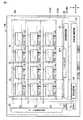
図9乃至図14は、映像データ提供装置410から提供されるシリアルデータの各種の伝送形態例を示している。伝送ラインにおいては、映像データ、制御データ、アドレスデータなどが一定のルールで伝送されるが映像データには各種のタイプが存在するので以下に説明する。 9 to 14 show various transmission forms of serial data provided from the video
SCSは、あるまとまったシリアルデータが伝送される期間を指定する期間指定信号(同期信号或いはイネーブル期間信号と称してもよい)である。このSCSは、例えばシリアルデータSIに含まれる例えばフレーミング信号(一定のパルスパターンで送られてくる同期引き込み用の信号:図では省略)をシステムが検出したときに立ち上がる。
SIは、シリアルデータであり、先のフレーミング信号、モード制御データ(M0、M1・・・M5)、ゲートラインアドレス指定データ(AG9、AG8、AG7、・・・AG0)、映像データ、ダミーデータ、その他などが含まれる。さらにデータの境界を示す同期クロック、エラー訂正コードなどが含まれてもよい。The SCS is a period specifying signal (which may be referred to as a synchronization signal or an enable period signal) that specifies a period during which certain serial data is transmitted. This SCS rises when the system detects, for example, a framing signal (synchronous pull-in signal sent in a fixed pulse pattern: omitted in the figure) included in the serial data SI, for example.
SI is serial data, the previous framing signal, mode control data (M0, M1,... M5), gate line address designation data (AG9, AG8, AG7,... AG0), video data, dummy data, Others are included. Furthermore, a synchronous clock indicating the data boundary, an error correction code, and the like may be included.
SCLKは、シリアルクロック(或いはシステムクロック)であり、シリアルデータに同期しており、シリアルデータをサンプリングすることができる。上記のシリアルデータを受け取るシリアルデータ処理部では、8ビット単位のシリアルデータを判断し、映像データ、制御データ、アドレス指定データなどを分離する。映像データは、後述するデータ変換部(データ制御部と称してもよい)に伝送される。制御データ、アドレス指定データなどは、制御装置CP内で出力タイミングなどが調整され、信号供給回路110、ゲート線駆動回路GDなどに送られる。 SCLK is a serial clock (or system clock), is synchronized with serial data, and can sample serial data. The serial data processing unit that receives the serial data determines 8-bit serial data and separates video data, control data, address designation data, and the like. The video data is transmitted to a data conversion unit (which may be referred to as a data control unit) described later. Control data, addressing data, and the like are sent to the
図9は、映像データ提供装置410から送られてくるシリアルデータに含まれる映像データが、映像データR、G、Bの例である。このタイプの映像データのモードは、3ビットデータモード(3bit−data mode)と称される。
シリアルデータの中の6クロック分のM0−M5は、モードテーブル(Mode table)を構成するデータである。この伝送形態の場合は、モードテーブルがM0=H(ハイレベル)、M1=L(ローレベル)/H(ハイレベル)、M2、M3、M4=L(ローレベル)、M5=−(不定)を示している。この情報は映像データが、映像データR、G、Bのタイプであることを意味する。FIG. 9 is an example in which the video data included in the serial data sent from the video
M0 to M5 for 6 clocks in the serial data are data constituting a mode table. In the case of this transmission form, the mode table is M0 = H (high level), M1 = L (low level) / H (high level), M2, M3, M4 = L (low level), M5 =-(indefinite) Is shown. This information means that the video data is of the video data R, G, B type.
またこの伝送形態では、SCSが指定する1つの指定期間に、単一ライン(1ラインと称してもよい)分の映像データが伝送されてくる。この伝送形態は、シングルライン更新モード(Single lines update mode)と称される。即ち、この伝送形態は、SCSが指定する1つの指定期間に、1ライン分(X方向の1ライン分)の映像データR、G、Bが伝送される。この伝送形態は、例えば信号供給回路及び又は制御装置により認識される。信号供給回路及び又は制御装置は、データ伝送期間(Data transfer period)のダミーデータの連続期間(例えば7クロック期間をオーバーしたとき)を判定することで、認識される。即ちSCSが指定する1つの指定期間に1ライン分が更新されることが認識される。 In this transmission mode, video data for a single line (also referred to as one line) is transmitted in one designated period designated by the SCS. This transmission form is referred to as a single line update mode. That is, in this transmission form, video data R, G, and B for one line (one line in the X direction) are transmitted in one designated period designated by the SCS. This transmission form is recognized, for example, by a signal supply circuit and / or a control device. The signal supply circuit and / or the control device can be recognized by determining a continuous period of dummy data (for example, when 7 clock periods are exceeded) in the data transfer period. That is, it is recognized that one line is updated in one designated period designated by the SCS.
図9に示すように、SCSが立ち上がる(論理1になる)と、システムクロックに同期してM0−M5の配列が到来する。このM0−M5のデータ配置期間は、モード選択期間(Mode select period)と称される。次に、ゲートラインアドレス指定データ(AG9、AG8、AG7、・・・AG0)が続く、このデータ配置期間は、ゲートラインアドレス選択期間(Gate line address select period)と称される。このゲートラインアドレス指定データにより、次に到来する映像データの書き込みラインが決定される。次に映像データR、G、Bが繰り返し配置されて到来する、図では、データD1R、D1G、D1B、D2R、D2G、D2B、D3R、D3G、D3B・・・・DnR、DnG、DnBとして示している。この期間は、データ書き込み期間(Data write period)と称される。次の期間は、データ伝送期間(Data transfer period)と称され、上記のデータが、データ処理部で抽出され、映像データが表示パネルに書き込むまでの猶予を与える期間である。 As shown in FIG. 9, when the SCS rises (becomes logic 1), an array of M0 to M5 arrives in synchronization with the system clock. The data arrangement period from M0 to M5 is referred to as a mode selection period (Mode select period). Next, this data arrangement period in which the gate line address designation data (AG9, AG8, AG7,... AG0) continues is referred to as a gate line address selection period (Gate line address select period). The gate line addressing data determines the next video data write line. Next, video data R, G, and B are repeatedly arranged and arrived. In the figure, data D1R, D1G, D1B, D2R, D2G, D2B, D3R, D3G, D3B,... Are shown as DnR, DnG, and DnB. Yes. This period is referred to as a data write period. The next period is referred to as a data transfer period, and is a period in which the above data is extracted by the data processing unit and video data is written on the display panel.
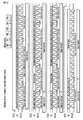
図10は、映像データ提供装置410から送られてくるシリアルデータに含まれる映像データが、映像データR、G、Bの例である。このタイプの映像データのモードは、3ビットデータモード(3bit−data mode)と称される。この場合は映像に関するモードテーブルがM0=H、M1=L/H、M2、M3、M4=L、M5=−(不定)である。 FIG. 10 is an example in which the video data included in the serial data sent from the video
この伝送形態の場合は、SCSが指定する1つの指定期間に、複数ライン分(Y方向の複数ライン分)の映像データR、G、Bが伝送されてくる。即ち、SCSが指定する1つの指定期間に複数ライン分が更新される。この伝送形態は、マルチプルライン更新モード(Multiple lines update mode)と称される。したがって、この伝送形態の場合は、ゲートラインアドレス選択期間(Gate line address select period)とデータ書き込み期間(Data write period)とのペアが複数回繰り替えしている。図10では、1回目のゲートラインアドレス選択期間のデータにより、指定されるゲートラインをGate 1st lineとして示し、2回目のゲートラインアドレス選択期間のデータにより、指定されるゲートラインをGate 2nd lineとして示し、m回目のゲートラインアドレス選択期間のデータにより、指定されるゲートラインをGate mth lineとして示している。他方式は、図9に示した例と同じである。 In the case of this transmission form, video data R, G, and B for a plurality of lines (for a plurality of lines in the Y direction) are transmitted in one designated period designated by the SCS. That is, a plurality of lines are updated in one designated period designated by the SCS. This transmission form is referred to as a multiple line update mode. Therefore, in this transmission mode, a pair of a gate line address selection period (Gate line address select period) and a data write period (Data write period) is repeated a plurality of times. In FIG. 10, the gate line specified by the data of the first gate line address selection period is designated as Gate 1st line, and the gate line designated by the data of the second gate line address selection period is designated as Gate 2nd line. The gate line designated by the data of the m-th gate line address selection period is indicated as Gate mth line. The other method is the same as the example shown in FIG.
図11は、映像データ提供装置410から送られてくるシリアルデータに含まれる映像データが、モノクロの例である。このタイプの映像データのモードは、1ビットデータモード(1bit−data mode)と称される。この場合、映像に関するモードテーブルは、M0=H、M1=L/H、M2、M3=L、M4=H、M5=−(不定)である。 FIG. 11 shows an example in which the video data included in the serial data sent from the video
ここでの映像データは、SCSが指定する1つの指定期間に、単一ライン(1ラインと称してもよい)分が伝送されてくる。この伝送形態は、シングルライン更新モード(Single lines update mode)と称される。他の項目に関する方式は、図9、図10等に示した例と同じである。 The video data here is transmitted for a single line (may be referred to as one line) in one designated period designated by the SCS. This transmission form is referred to as a single line update mode. The system relating to other items is the same as the example shown in FIGS.
図12は、映像データ提供装置410から送られてくるシリアルデータに含まれる映像データが、モノクロの例である。このタイプの映像データのモードは、1ビットデータモード(1bit−data mode)と称される。映像に関するモードテーブルは、M0=H、M1=L/H、M2、M3=L、M4=H、M5=−(不定)である。 FIG. 12 is an example in which the video data included in the serial data sent from the video
一方、ここでの映像データは、SCSが指定する1つの指定期間に、複数ライン(マルチラインと称してもよい)分が伝送されてくる。この伝送形態は、マルチライン更新モード(Multiple lines update mode)と称される。他の項目に関する方式は、図9、図10、図11等に示した例と同じである。 On the other hand, the video data here is transmitted for a plurality of lines (also referred to as multi-lines) in one designated period designated by the SCS. This transmission mode is referred to as a multiple line update mode. The system relating to other items is the same as the example shown in FIGS.
図13は、映像データ提供装置410から送られてくるシリアルデータに含まれる映像データが、映像データR、G、B及びダミー(DUM)の例である。このタイプの映像データのモードは、4ビットデータモード(4bit−data mode)と称される。映像に関するモードテーブルは、M0=H、M1=L/H、M2、M3=H、M4=−(不定)、M5=−(不定)である。この伝送形態では、SCSが指定する1つの指定期間に、単一ライン(1ラインと称してもよい)分の映像データが伝送されてくる。この伝送形態は、シングルライン更新モード(Single lines update mode)と称される。他の項目に関する方式は、図9、図10等に示した例と同じである。 FIG. 13 shows an example in which the video data included in the serial data sent from the video
図14は、映像データ提供装置410から送られてくるシリアルデータに含まれる映像データが、映像データR、G、B及びダミー(DUM)の例である。このタイプの映像データのモードは、4ビットデータモード(4bit−data mode)と称される。映像に関するモードテーブルは、M0=H、M1=L/H、M2、M3=H、M4=−(不定)、M5=−(不定)である。この伝送形態では、SCSが指定する1つの指定期間に、複数ライン(マルチラインと称してもよい)分の映像データが伝送されてくる。この伝送形態は、マルチライン更新モード(Multi lines update mode)と称される。他の項目に関する方式は、図9、図10、図11、図12、図13等に示した例と同じである。 FIG. 14 shows an example in which the video data included in the serial data sent from the video
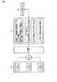
図15は、上記したシリアルデータを受信して処理する信号供給回路110の一実施形態を示している。入力端子2103には、シリアルデータが入力される。入力端子2103は、データ解析・分離制御回路2201と、シリアルデータ処理回路2200に接続されている。データ解析・分離制御回路2201は、図10乃至図14で説明したデータモードのうちどのデータモードのシリアルデータが入力しているかを判断することができる。データ解析・分離制御回路2201は、SCS及びSCLKに同期して動作し、仕様書により予め取り決められているルールに従い区分信号を生成する。そしてこの区分信号により、モード制御データ(M0、M1・・・M5)、ゲートラインアドレス指定データ(AG9、AG8、AG7、・・・AG0)、映像データ、ダミーデータ、その他を分離することができる。 FIG. 15 shows an embodiment of a
データ解析・分離制御回路2201は、入力したシリアルデータの中からモードテーブルを判定し、図9乃至図14に示したシリアルデータのうちどのタイプの映像データ(4ビット或いは3ビット或いは1ビットデータモードと称した)であり、どの更新モードであるかを判定することができる。また、映像データの書き込み先であるゲートラインのアドレスを指定するゲートラインアドレスデータを分離することができる。このアドレスデータは、ゲート線駆動回路GDなどを制御するクロック及びタイミングパルス生成回路123に与えられる。クロック及びタイミングパルス生成回路123は、ゲートラインアドレスデータに基づいて、ゲート線駆動回路GDを制御する。 The data analysis /
なお入力端子2103に入力するシリアルデータに含まれるシリアル映像データのタイプや更新モードであるかが予め特定されているときは、データ解析・分離制御回路2201は、動作モード設定端子MT1からタイプや更新モードを示すモードを識別した情報を与えることができる。このモード識別情報は、ユーザが入力してもよいし、製造者がこの表示装置の工場出荷時に入力してもよい。なおこのモード識別情報が設定されていない場合は、入力シリアルデータを用いて、シリアル映像データのタイプや更新モードが自動的に識別される。 If it is specified in advance whether the type or update mode of the serial video data included in the serial data input to the
モード制御回路1103には、データ解析・分離制御回路2201から映像データのタイプ及び更新モード情報が与えられる。モード制御回路1103は、表示パネルの仕様書情報(表示パネルPNLのタイプなどを識別した情報)を動作モード設定端子MT2から受け取ることができる。タイプ識別情報は、ユーザが入力してもよいし、製造者がこの表示装置の工場出荷時に入力してもよい。なおこのタイプ識別情報が設定されていない場合は、入力シリアルデータを用いて、シリアル映像データのタイプや更新モードが自動的に識別されてもよい。表示パネルPNLは、例えば図6、図7、図8に示したようなタイプがある。モード制御回路1103は、映像データのタイプ及び更新モード情報に基づいて、シリアルデータから映像データを切り出すタイミング信号を生成することができる。 The
シリアルデータ処理回路2200においては、図9−図14で示したようなシリアル入力される映像データが、パラレルデータD1〜D8に変換されて出力される。パラレルデータD1〜D8は、データ変換部2300に入力され一旦ラッチされる。データ変換部2300は、振り分け回路2301を含む。振り分け回路2301は、データ変換部2300内部にラッチされた各データを、適切なカラーの副画素に振り分けて、後段の水平ライン分を保持するラッチ回路に出力する。 In the serial
なおモード制御回路1103とデータ解析・分離制御回路2201とは、一体化されて構成されてもよい。そして前記一体化ブロックが入力適応制御回路2205と称されてもよい。 Note that the
図16は、図15に示したシリアルデータ処理回路2200の内部のシリアルパラレル変換回路の一例を示している。シリアルデータ処理回路2200は、8ビット単位の入力データを処理するために、直列接続された例えば8つのレジスタReg21−Reg28を含み、8個のラッチパルス(サンプリングパルスと称してもよい)を連続的に出力するとともに、8個のラッチパルスをサイクリックに発生することができる。そのために最終段のレジスタReg28の出力が初段のレジスタReg21へ帰還する帰還ループ2211を備える。さらにこの帰還ループの211途中には、入力する映像データのデータモード(図9−図14に示す)に応じて、動作モード(ラッチタイミング、データサンプルタイミング、サンプリング速度と称してもよい)を切り替えられるように、スイッチSW11、SW12を備える。 FIG. 16 shows an example of the serial-parallel conversion circuit inside the serial
スイッチSW12は、レジスタReg26の出力又はレジスタReg28の出力を帰還させることができる。スイッチSW11は、レジスタReg22の出力又は、レジスタReg26の出力又は、レジスタReg28の出力を帰還させることができる。 The switch SW12 can feed back the output of the register Reg26 or the output of the register Reg28. The switch SW11 can feed back the output of the register Reg22, the output of the register Reg26, or the output of the register Reg28.
また、シリアルデータ処理回路2200は、8連続するシリアルデータ(映像データ)を順次ラッチできるように8つのラッチ回路Lat21−Lat28を含む。8つのラッチ回路Lat21−Lat28は、8つのレジスタReg21−Reg28からのラッチパルスに基づいて、入力端子2103からの映像データを次々とラッチすることができる。ラッチ回路Lat21−Lat28がラッチした、データD1〜D8は、データ変換部2300に入力する。 Further, the serial
入力端子2103は、ラッチ回路Lat21−Lat28のデータ入力端子に対して、スイッチSW31を介して接続されている。このスイッチSW01は、図9乃至図14で示した映像データ(D1R、D1G,D1B・・・・DnB)が入力端子2103に入力したときにオンとなる。またスイッチSW02は、レジスタReg21に初期値“1”を入力するためと、後段のレジスタからの帰還データ“1”を巡回させるために利用される。レジスタReg21−Reg28は、シリアルクロックSCLKと同相のクロックで駆動されるが、図16では省略している。 The
今、図16の状態では、スイッチSW12がレジスタReg26の出力データを帰還するように制御されている。この接続状態においては、ラッチ回路Lat21−Lat26でラッチ動作が行われる。ラッチ回路Lat27、Lat28は、使用されない。したがって、ラッチデータとしては、3の倍数である6個のデータD1−D6が巡回して出力されることになる。この動作は、入力映像データが3ビットデータモードである場合に有効である。 Now, in the state of FIG. 16, the switch SW12 is controlled to feed back the output data of the register Reg26. In this connected state, a latch operation is performed in the latch circuits Lat21 to Lat26. The latch circuits Lat27 and Lat28 are not used. Therefore, six pieces of data D1 to D6 that are multiples of 3 are cyclically output as the latch data. This operation is effective when the input video data is in the 3-bit data mode.
もし、スイッチSW12がレジスタReg28の出力データを帰還するように制御された場合は、ラッチ回路Lat21−Lat28でラッチ動作が行われる。したがって、ラッチデータとしては、4の倍数である8個のデータD1−D8が巡回して出力されることになる。この動作は、入力映像データが4ビットデータモードである場合に有効である。
もし、スイッチSW11がレジスタReg22の出力データを帰還するように制御された場合は、ラッチ回路Lat21、Lat22でラッチ動作が行われる。したがって、ラッチデータとしては、1の倍数である2個のデータD1、D2が巡回して出力されることになる。この動作は、入力映像データが1ビットデータモードである場合に有効である。If the switch SW12 is controlled to feed back the output data of the register Reg28, the latch operation is performed by the latch circuits Lat21 to Lat28. Therefore, eight pieces of data D1 to D8, which are multiples of 4, are cyclically output as the latch data. This operation is effective when the input video data is in the 4-bit data mode.
If the switch SW11 is controlled to feed back the output data of the register Reg22, a latch operation is performed in the latch circuits Lat21 and Lat22. Therefore, as the latch data, two pieces of data D1 and D2 that are multiples of 1 are cyclically output. This operation is effective when the input video data is in the 1-bit data mode.
上記のようにラッチされ、パラレルデータとなったラッチデータは、データ変換部2300に入力され、適切な信号線S(S1−Sm)に振り分けられる。この動作は、入力映像データが1ビットデータモードである場合に有効である。
Cyc1は、入力映像データが1ビットデータモードである場合の、データD1、D2出力の巡回を示している。Cyc6は、入力映像データが3ビットデータモードである場合の、データD1―D6出力の巡回を示している。Cyc6は、入力映像データが4ビットデータモードである場合の、データD1―D8出力の巡回を示している。The latch data latched as described above and converted into parallel data is input to the
Cyc1 indicates a cycle of outputting data D1 and D2 when the input video data is in the 1-bit data mode. Cyc6 indicates a cycle of data D1-D6 output when the input video data is in the 3-bit data mode. Cyc6 indicates a cycle of data D1-D8 output when the input video data is in the 4-bit data mode.
図17は、データ変換部2300の内部構成の一例を示している。ラッチパルス生成回路2305、データラッチ回路2306を含む。このデータ変換部2300のデータラッチ回路2306には、シリアルデータ処理部2200からシリアルパラレル変換されたデータD1−D8が入力する。
これらのデータD1−D8は、ラッチ回路Lat41−Lat48でラッチされることが可能である。ラッチ回路Lat41−Lat48に対するラッチパルスLap41−Lap48としては、複数のレジスタReg41−Reg44により生成される巡回サンプリングパルス(ラッチパルスと称してもよい)が用いられる。FIG. 17 shows an example of the internal configuration of the
These data D1-D8 can be latched by the latch circuits Lat41-Lat48. As the latch pulses Lap41-Lap48 for the latch circuits Lat41-Lat48, cyclic sampling pulses (also referred to as latch pulses) generated by a plurality of registers Reg41-Reg44 are used.
ラッチパルスLap41−Lap48を生成する回路は、直列接続されたレジスタReg41−Reg48、スイッチSW21、SW22、SW23などを含む。スイッチSW21は、ラッチパルスを生成するスタート時に初段のレジスタReg21にデータ1をセットするためのスイッチである。スイッチSW23は、データモードに応じて最終段のレジスタReg48の出力又は第6段目のレジスタReg46の出力を帰還させるためのスイッチである。スイッチSW22は、第2段目のレジスタReg42又はスイッチSW23からの出力を初段のレジスタReg41に帰還させるためのスイッチである。 A circuit for generating the latch pulses Lap41-Lap48 includes registers Reg41-Reg48, switches SW21, SW22, SW23 and the like connected in series. The switch SW21 is a switch for setting
4ビットデータモードの入力映像データが入力するときは、スイッチSW22、SW23は最終段のレジスタReg48の出力を初段のレジスタReg41に帰還するように制御される。これにより、ラッチ回路Lat41−Lat48は入力データD1−D8を巡回的にラッチする。
3ビットデータモードの入力映像データが入力するときは、スイッチSW22、SW23は6段目のレジスタReg46の出力を初段のレジスタReg41に帰還するように制御される。これにより、ラッチ回路Lat41−Lat46は入力データD1−D6を巡回的にラッチする。データD7、D8は、使用されない。When input video data in the 4-bit data mode is input, the switches SW22 and SW23 are controlled to feed back the output of the last-stage register Reg48 to the first-stage register Reg41. As a result, the latch circuits Lat41 to Lat48 cyclically latch the input data D1 to D8.
When input video data in the 3-bit data mode is input, the switches SW22 and SW23 are controlled to feed back the output of the sixth-stage register Reg46 to the first-stage register Reg41. As a result, the latch circuits Lat41 to Lat46 cyclically latch the input data D1 to D6. Data D7 and D8 are not used.
1ビットデータモードの入力映像データが入力するときは、スイッチSW22、SW23は2段目のレジスタReg42の出力を初段のレジスタReg41に帰還するように制御される。これにより、ラッチ回路Lat41−Lat42は入力データD1−D2を巡回的にラッチする。データD3―D8は、使用されない。 When input video data in the 1-bit data mode is input, the switches SW22 and SW23 are controlled so as to feed back the output of the second-stage register Reg42 to the first-stage register Reg41. As a result, the latch circuits Lat41 to Lat42 cyclically latch the input data D1 to D2. Data D3-D8 are not used.
ラッチ回路Lat31−Lat48から出力されるラッチデータは、振り分け回路2301に入力される。振り分け回路2301は、表示パネルのタイプに応じて、ラッチデータ(データR、G、B、又はデータR、G、B、W、又はデータ1)などを適切な信号線S(S1−Sm)に振り分け処理することができる。振り分け回路2301は、モード制御回路1103で判定された映像データのビットデータモードと、システムにて使用されている表示パネルの形式或いはタイプに応じて、映像データR、G、B、Wなどの振り分け処理を実行する。また振り分け回路2301は、同時化パルスSt_Pにより、ラッチ回路群からのデータを同時に取り込むことができる。同時化パルスSt_Pもモード制御回路1103或いはデータ解析・分離回路2201で生成されている。 The latch data output from the latch circuits Lat31 to Lat48 is input to the
振り分け回路2301の出力(出力パラレル映像データと称することができる)は、後段の水平ライン分を保持するラッチ回路に出力される。即ち、振り分けられた各データ(出力パラレル映像データ)は、1水平ライン分の副画素データを保持するラッチ回路群に出力され、供給すべきゲートラインが特定されたとき、一斉に対応する信号線に出力される。 The output of the distribution circuit 2301 (which can be referred to as output parallel video data) is output to a latch circuit that holds the horizontal line of the subsequent stage. That is, each distributed data (output parallel video data) is output to a latch circuit group that holds sub-pixel data for one horizontal line, and when a gate line to be supplied is specified, the corresponding signal line Is output.
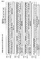
図18は、信号供給回路110に入力する映像データのデータモードの種類を示している。映像データのデータモードとしては、図9−図14で示したように4ビットデータモード、3ビットデータモード、1ビットデータモードが存在する。 FIG. 18 shows types of data modes of video data input to the
一方、信号供給回路110から出力される映像データを表示する表示パネルのタイプとしては、RGBWのカラーフィルタ備えた表示パネルPNL、RGBのカラーフィルタを備えた表示パネルPNL、モノクロの表示パネルPNLのうち、ユーザの選択によりいずれかが作用される。モノクロの表示パネルPNLの場合、階調表示が可能なパネル、或いは、階調表示しないパネルがある。 On the other hand, display panel types for displaying video data output from the
図19は、表示パネルPNLとしてRGBWのカラーフィルタ備えた表示パネルPNLが採用されている表示装置の例を示している。この場合、信号供給回路110としては、次のように入力映像データを変換処理することができる。 FIG. 19 shows an example of a display device that employs a display panel PNL provided with RGBW color filters as the display panel PNL. In this case, the input video data can be converted by the
(A_4)4ビットデータモードの映像データ(図13、図14で示した映像データ)が入力した場合は、信号供給回路110は、ダミーデータをカット(破棄)して、RGBデータをそのまま対応する画素へ供給する。このときは、信号供給回路110のシリアルデータ処理回路2200では、すべての8ビットシリアルデータD1−D8がシリアルパラレル変換される(図16参照)。またデータ変換部2300のデータラッチ回路2306は、すべての8ビットシリアルデータD1−D8がサイクル的にラッチされる(図17参照)。さらにデータ変換部2300は、フィルタWの画素に供給すべき映像データを近隣のRGBデータから作成する。例えば、Rデータ、Gデータ及びBデータが全て”1”、又は、2つ以上が”1”で供給されたときに、”1”のWデータを作成してもよい。 (A — 4) When video data in the 4-bit data mode (video data shown in FIGS. 13 and 14) is input, the
(B_4)3ビットデータモードの映像データ(図9、図10で示した映像データ)が入力した場合は、信号供給回路110は、RGBデータをそのまま対応する画素へ供給する。このときは、信号供給回路110のシリアルデータ処理回路2200では、6ビットシリアルデータD1−D6がシリアルパラレル変換される。(図16参照)。またデータ変換部2300のデータラッチ回路2306は、6ビットシリアルデータD1−D6がサイクル的にラッチされる(図17参照)。さらにこの場合は、RGBの映像データが用いられて、輝度データ(W)データが生成される。これにより、表示パネルPNLのRGBWのカラーフィルタに他出力する映像データを準備することができる。 (B — 4) When video data in the 3-bit data mode (video data shown in FIGS. 9 and 10) is input, the
(C_4)1ビットデータモードの映像データ(図11、図12で示した映像データ)が入力した場合は、信号供給回路110は、映像データを例えば、フィルタWの画素へ供給する。或いは、映像データを例えば、フィルタR又はG又はBの画素へ供給する(この時は単色R又はB又はGの単色表示となる)。或いは、映像データの”1”又は”0”にすべて応じて、隣り合うRGBWに”1”、又は隣り合うRGBWにすべて”0”を供給する。 (C — 4) When video data in the 1-bit data mode (video data shown in FIGS. 11 and 12) is input, the
図20は、表示パネルPNLとしてRGBのカラーフィルタ備えた表示パネルPNLが採用されている表示装置の例を示している。この場合、信号供給回路110としては、次のように入力映像データを変換処理することができる。 FIG. 20 shows an example of a display device in which a display panel PNL provided with RGB color filters is adopted as the display panel PNL. In this case, the input video data can be converted by the
(A_3)4ビットデータモードの映像データ(図13、図14で示した映像データ)が入力した場合は、信号供給回路110は、ダミーデータをカットして、RGBデータをそのまま対応する画素へ供給する。このときは、信号供給回路110のシリアルデータ処理回路2200では、8ビットシリアルデータD1−D8がシリアルパラレル変換される。(図16参照)。またデータ変換部2300のデータラッチ回路2306は、8ビットシリアルデータD1−D8がサイクル的にラッチされる(図17参照)。ただし、振り分け回路2301においては、ダミーデータがカットされる。 (A_3) When 4-bit data mode video data (video data shown in FIGS. 13 and 14) is input, the
(B_3)3ビットデータモードの映像データ(図9、図10で示した映像データ)が入力した場合は、信号供給回路110は、RGBデータをそのまま対応する画素へ供給する。このときは、信号供給回路110のシリアルデータ処理回路2200では、6ビットシリアルデータD1−D6がシリアルパラレル変換される。(図16参照)。またデータ変換部2300のデータラッチ回路2306は、6ビットシリアルデータD1−D6がサイクル的にラッチされる(図17参照)。 (B — 3) When video data in the 3-bit data mode (video data shown in FIGS. 9 and 10) is input, the
(C_3)1ビットデータモードの映像データ(図11、図12で示した映像データ)が入力した場合は、信号供給回路110は、映像データを例えば、フィルタR又はG又はBの画素へ供給する(この時は単色R又はB又はGの単色表示となる)。或いは、映像データの”1”又は”0”に応じて、隣り合うRGBにすべて”1”、又は隣り合うRGBにすべて”0”を供給する。 (C — 3) When video data in the 1-bit data mode (video data shown in FIGS. 11 and 12) is input, the
図21は、表示パネルPNLとしてモノクロの表示パネルPNLが採用されている表示装置の例を示している。この場合、信号供給回路110としては、次のように入力映像データを変換処理することができる。 FIG. 21 shows an example of a display device in which a monochrome display panel PNL is adopted as the display panel PNL. In this case, the input video data can be converted by the
(A_3)4ビットデータモードの映像データ(図13、図14で示した映像データ)が入力した場合は、信号供給回路110は、ダミーデータをカットして、RGBデータをそのままモノクロの画素へ供給する。このときは、信号供給回路110のシリアルデータ処理回路2200では、8ビットシリアルデータD1−D8がシリアルパラレル変換される。(図16参照)。またデータ変換部2300のデータラッチ回路2306は、8ビットシリアルデータD1−D8がサイクル的にラッチされる(図17参照)。ただし、振り分け回路2301においては、ダミーデータがカット(破棄)される。なお、このモードにおいては、ダミーデータがカットされているため、階調は3階調となる。一方で、1画素あたりに4つの副画素(例えばRGBW)があれば、RGBWデータを転送した場合は、4階調のモノクロ画像を表現出来る。 (A — 3) When video data in the 4-bit data mode (video data shown in FIGS. 13 and 14) is input, the
(B_3)3ビットデータモードの映像データ(図9、図10で示した映像データ)が入力した場合は、信号供給回路110は、RGBデータをそのままモノクロの画素へ供給する。このときは、信号供給回路110のシリアルデータ処理回路2200では、6ビットシリアルデータD1−D6がシリアルパラレル変換される。(図16参照)。またデータ変換部2300のデータラッチ回路2306は、6ビットシリアルデータD1−D6がサイクル的にラッチされる(図17参照)。 (B — 3) When video data in the 3-bit data mode (video data shown in FIGS. 9 and 10) is input, the
(C_3)1ビットデータモードの映像データ(図11、図12で示した映像データ)が入力した場合は、信号供給回路110は、映像データをそのまま各画素に供給する。
上記した信号供給回路110における処理は、ハードウエアにより実現してもよいし、メモリ、メモリの読出し書き出し回路をソフトウエアにより制御して実現してもよい。(C — 3) When video data in the 1-bit data mode (video data shown in FIGS. 11 and 12) is input, the
The processing in the
図22は、RGBのカラーフィルタを備える表示パネルPNLが採用され、そして映像データ提供装置410から4ビットデータモードの映像データが供給された場合、並列化されたデータD1−D8が振り分け回路2301に同時化されて取り込まれるときの動作を示すタイミング図である。4ビットデータモードにおいては、映像データR、G、B、DU(ダミー)がサイクリックに信号供給回路110に入力する。よって、シリアルデータ処理回路2200からデータD1−D8が順次出力される。この場合は、図16に示したシフトレジスタのデータ転送系路は、8つのレジスタReg21−Reg28のすべてが用いられる、つまりスイッチSW21は、レジスタReg28の出力を選択し、スイッチSW11は、スイッチSW21の出力を選択するように制御される。また図17に示したシフトレジスタのデータ転送系路も、8つのレジスタReg41−Reg48が用いられる、つまりスイッチSW23は、レジスタReg28の出力を選択し、スイッチSW21は、スイッチSW23の出力を選択するように制御される。 In FIG. 22, when a display panel PNL having RGB color filters is adopted and video data in the 4-bit data mode is supplied from the video
そして図17に示したように、データD1−D8は、データ変換部3300のラッチ回路Lat41−Lat48に順次ラッチされる。そして、これらのデータは、振り分け回路2301の入力段で同時化パルスSt_Pにより同時化される。
同時化パルスのタイミングは、図22に示すように4つのデータがラッチされた後の時点で発生する。これにより、4つの映像データR、G、B、DUが1つの単位として振り分け回路2301に入力する。図22の例は、4つの映像データ(R1、G1、B1、DU1)、4つの映像データ(R2、G2、B2、DU2)、4つの映像データ(R3、G3、B3、DU3)・・・・が順次振り分け回路2301にサンプルされる例を示している。
なお振り分け回路2301において、ダミーデータ(DU)は、破棄される。As shown in FIG. 17, the data D1 to D8 are sequentially latched in the latch circuits Lat41 to Lat48 of the data conversion unit 3300. These data are synchronized by the synchronization pulse St_P at the input stage of the
The timing of the synchronization pulse occurs at a time point after the four data are latched as shown in FIG. As a result, the four video data R, G, B, and DU are input to the
In the
図23は、RGBのカラーフィルタを備える表示パネルPNLが採用され、そして映像データ提供装置410から3ビットデータモードの映像データが供給された場合、並列化されたデータD1−D6が振り分け回路2301に同時化されて取り込まれるときの動作を示すタイミング図である。3ビットデータモードにおいては、映像データR、G、Bがサイクリックに信号供給回路110に入力する。よって、シリアルデータ処理回路2200からデータD1−D6が順次出力される。この場合は、図16に示したシフトレジスタのデータ転送系路は、6つのレジスタReg21−Reg26が用いられる、つまりスイッチSW21は、レジスタReg26の出力を選択し、スイッチSW11は、スイッチSW21の出力を選択するように制御される。また図17に示したシフトレジスタのデータ転送系路も、6つのレジスタReg41−Reg46が用いられる、つまりスイッチSW23は、レジスタReg26の出力を選択し、スイッチSW21は、スイッチSW23の出力を選択するように制御される。 In FIG. 23, when a display panel PNL having RGB color filters is employed, and video data in the 3-bit data mode is supplied from the video
そして図17に示したように、データD1−D6は、データ変換部3300のラッチ回路Lat41−Lat46に順次ラッチされる。そして、これらのデータは、振り分け回路2301の入力段で同時化パルスSt_Pにより同時化される。
同時化パルスのタイミングは、図23に示すように、例えば到来する映像データRと次の映像データGの間と、到来する映像データBと次の映像データRとの間である。これにより、映像データ(D1=R1、D2=G1、D3=B1)、映像データ(D4=R2、D5=G2、D6=B2)、映像データ(D1=R3、D2=G3、D3=B3)、映像データ(D4=R4、D5=G4、D6=B4)・・・・が順次振り分け回路2301にて処理される。As shown in FIG. 17, the data D <b> 1 to D <b> 6 are sequentially latched by the latch circuits Lat <b> 41 to Lat <b> 46 of the data conversion unit 3300. These data are synchronized by the synchronization pulse St_P at the input stage of the
The timing of the synchronization pulse is, for example, between the incoming video data R and the next video data G, and between the incoming video data B and the next video data R, as shown in FIG. Thereby, video data (D1 = R1, D2 = G1, D3 = B1), video data (D4 = R2, D5 = G2, D6 = B2), video data (D1 = R3, D2 = G3, D3 = B3) , Video data (D4 = R4, D5 = G4, D6 = B4),... Are sequentially processed by the
図24は、RGBのカラーフィルタを備える表示パネルPNLが採用され、そして映像データ提供装置410から1ビットデータモードの映像データが供給された場合、並列化されたデータD1−D2が振り分け回路2301に同時化されて取り込まれるときの動作を示すタイミング図である。1ビットデータモードにおいては、シリアル映像データ(1又は0)が8ビットを単位としてサイクリックに信号供給回路110に入力する。この場合は、シリアルデータ処理回路2200からデータD1−D2が順次出力される。つまりこの場合は、図16に示したシフトレジスタのデータ転送系路は、2つのレジスタReg21−Reg22が用いられるもので、スイッチSW11は、レジスタReg22の出力を選択するように制御される。スイッチSW12は、任意である。また図17に示したシフトレジスタのデータ転送系路も、2つのレジスタReg41−Reg42が用いられる、つまりスイッチSW22は、レジスタReg22の出力を選択するように制御される。スイッチSW23は、任意である。 In FIG. 24, when a display panel PNL having RGB color filters is adopted and video data in the 1-bit data mode is supplied from the video
そして図17に示したように、データD1−D2は、データ変換部3300のラッチ回路Lat41−Lat42に順次ラッチされる。そして、これらのデータは、振り分け回路2301の入力段で同時化パルスSt_Pにより同時化される。 As shown in FIG. 17, the data D1-D2 are sequentially latched by the latch circuits Lat41-Lat42 of the data conversion unit 3300. These data are synchronized by the synchronization pulse St_P at the input stage of the
同時化パルスは、図24に示すように、例えば到来する2つの映像データ毎に振り分け回路2301に供給される。
振り分け回路2301は、データD1=*1を副画素R、G、Bに振り分け、次のデータデータD2=*2を次の副画素R、G、Bに振り分け、次のデータデータD1=*3を次の副画素R、G、Bに振り分け、次のデータデータD2=*4を次の副画素R、G、Bに振り分け処理する。このように1水平ライン分のデータを順次取得する。As shown in FIG. 24, the synchronization pulse is supplied to the
The
図25A、図25B、図25Cは、それぞれ図22、図23、図24に示したデータ変換処理が実行される際に形成されるラッチパルス生成回路2305内のシフトレジスタReg41−Reg48のシフトデータ帰還系路の一例を示している。図25A、図25B、図25Cにおいては、それぞれシフトデータ帰還系路のスイッチSW22、SW23の状態が異なる。しかしスイッチSW22、SW23の説明は、それぞれ図22、図23、図24を説明したときにすでに説明したのでここでは省略する。
なお、シフトレジスタReg41−Reg48の配列は、一列に限定されるものではない。第1列をシフトレジスタReg41−Reg44、第2列をシフトレジスタReg44−Reg48として配置領域が狭くなるように工夫してもよい。25A, 25B, and 25C show the shift data feedback of the shift registers Reg41 to Reg48 in the latch
Note that the arrangement of the shift registers Reg41 to Reg48 is not limited to one line. The arrangement may be devised so that the arrangement region is narrowed with the first column as shift registers Reg41-Reg44 and the second column as shift registers Reg44-Reg48.
図26は、データ変換部2300内にさらにWデータ生成回路2307が設けられた他の実施形態を示している。データラッチ回路2306から出力される映像データR、G、Bを用いることで輝度に相当するWデータを生成することができる。例えば、映像データR、G、Bのそれぞれに係数a、b、cを乗算した後、以下の式のように加算すれば、映像データWを得ることができる。
W=a×R+b×G+c×B
この映像データWが振り分け回路2301により、適切な副画素Wに振り分けられる。振り分けられた映像データは、水平ラインデータラッチ回路2400に一旦保持される。そして、適切なタイミングで一斉に、指定された水平ラインに向けて、信号線を介して出力される。FIG. 26 shows another embodiment in which a W
W = a * R + b * G + c * B
This video data W is distributed to an appropriate sub-pixel W by the
上記のWデータ生成回路2307を備えることにより、副画素R、G、B、Wを備える表示パネルPNLが採用されたときに有効である。映像データ提供装置410が、映像データR、G、B、Wを提供するときは、Wデータ生成回路2307の動作は停止される。 The provision of the W
本発明は、上記実施形態に限定されるものではない。表示パネルがシアン、マゼンタ、青を備えるものであれば、データラッチ回路2306から出力されたRGBの映像データを、シアン、マゼンタ、青の成分データに変換する回路が設けられてもよい。 The present invention is not limited to the above embodiment. If the display panel includes cyan, magenta, and blue, a circuit that converts RGB video data output from the
上記したように本実施形態においては、以下のように多数の面で特徴的な構成が含まれる。
(1)本実施形態における信号供給回路は、複数の副画素の各々がメモリを有する表示パネルに用いられる、信号供給回路であって、外部から前記複数の副画素に対応するnビット単位の映像データを受け取り、前記第1映像データに基づいて、nビットよりも少ないmビットの単位で前記副画素用のデジタルデータを前記複数の副画素に供給する第1モードを備える。
(2)また上記(1)記載の信号供給回路では、前記映像データはシリアルデータであり、前記シリアルデータを前記複数の副画素に対応するデジタルデータにパラレル変換するパラレル変換部を備え、前記パラレル変換部は、前記nビットの前記映像データを前記mビットのデータに変換する。
(3)さらにまた、上記(1)又は(2)記載の信号供給回路では、ラッチ回路が3又は6個の場合があり、前記第1映像データはシリアルデータであり、前記シリアルデータを前記複数の副画素に対応するデジタルデータにパラレル変換するパラレル変換部を有し、前記パラレル変換部は、複数のラッチ回路を備え、前記パラレル変換に使用する前記複数のラッチ回路の個数は前記m個の整数倍(但し0倍を除く)である。
(4)また、上記(1)乃至(3)記載の何れかの信号供給回路では、使用するラッチ回路が6で副画素が3の場合があり、画素を構成する前記副画素の個数は、前記m個よりも少ないl個である。
(5)また、上記(1)乃至(4)記載の何れかの信号供給回路では、前記第1モードの前記第1映像データにダミーの映像データが含まれている。As described above, the present embodiment includes a characteristic configuration in many aspects as follows.
(1) The signal supply circuit according to the present embodiment is a signal supply circuit used in a display panel in which each of a plurality of subpixels has a memory, and an n-bit unit image corresponding to the plurality of subpixels from the outside. A first mode for receiving data and supplying the sub-pixel digital data to the plurality of sub-pixels in units of m bits smaller than n bits based on the first video data;
(2) In the signal supply circuit according to (1), the video data is serial data, and includes a parallel conversion unit that converts the serial data into digital data corresponding to the plurality of sub-pixels. The conversion unit converts the n-bit video data into the m-bit data.
(3) Furthermore, in the signal supply circuit described in (1) or (2) above, there may be three or six latch circuits, the first video data is serial data, and the serial data is converted into the plurality of serial data. A parallel conversion unit that performs parallel conversion to digital data corresponding to the sub-pixel, and the parallel conversion unit includes a plurality of latch circuits, and the number of the plurality of latch circuits used for the parallel conversion is the m pieces. It is an integer multiple (excluding 0 times).
(4) Further, in any of the signal supply circuits described in (1) to (3) above, there are cases where the number of latch circuits used is 6 and the number of subpixels is 3, and the number of the subpixels constituting the pixel is The number is less than m.
(5) In the signal supply circuit according to any one of (1) to (4), dummy video data is included in the first video data in the first mode.
(6)さらにまた、上記(1)記載の信号供給回路は、モノクロモードである第2モードを備え、前記第2モードは、外部から前記nビットの前記副画素に対応する第2映像データを受け取り、前記第2映像データに基づいて前記nビットよりも大きいk個の前記副画素用のデジタルデータを前記複数の副画素に供給するモードである。
(7)さらにまた、上記(6)記載の信号供給回路では、前記第2モードは、前記パラレル変換部は前記mビットの前記第1映像データを、1個の映像データ単位にパラレル変換する。
(8)さらにまた、上記(6)記載の信号供給回路では、前記nは前記lの整数倍ではない。好ましくは、前記nは8であり、前記mは3又は6であり、前記lは3である。
(9) さらに、上記(1)記載の信号供給回路では、外部シリアルデータから少なくともコマンド及びデータ区分信号を得るデータ入力適応制御回路2205と、前記入力適応制御回路2205からの前記データ区分信号に応じて、前記外部からの前記映像データを分離するシリアルデータ処理回路2202と、を有する。
(10)さらに上記(9)記載の信号供給回路は、前記コマンドに応じて動作モードを切り替えるモード制御回路1103を含む。(6) Furthermore, the signal supply circuit according to (1) includes a second mode which is a monochrome mode, and the second mode receives second video data corresponding to the n-bit sub-pixel from the outside. In this mode, digital data for k subpixels larger than the n bits is supplied to the plurality of subpixels based on the second video data.
(7) Furthermore, in the signal supply circuit according to (6), in the second mode, the parallel conversion unit performs parallel conversion of the m-bit first video data into one video data unit.
(8) Furthermore, in the signal supply circuit according to (6), n is not an integral multiple of l. Preferably, the n is 8, the m is 3 or 6, and the l is 3.
(9) Further, in the signal supply circuit described in (1) above, a data input
(10) The signal supply circuit according to (9) further includes a
(11)上記実施形態の表示装置は、シリアルデータが入力され、該シリアルデータに含まれるシリアル映像データをパラレル変換し、パラレル映像データを出力するシリアルデータ処理回路2200と、前記パラレル映像データをラッチして表示パネルに配列されている対応する各副画素に振り分け処理した、出力パラレル映像データを得るデータ変換部2300と、前記表示パネルの副画素配列のタイプ情報と、前記シリアルデータに含まれる前記シリアル映像データのモードに応じて、前記シリアルデータ処理回路2200のパラレル変換動作及び前記データ変換部2300の前記ラッチ及び振り分け処理を制御する入力適応制御回路2205を備える。
(12)また上記(11)記載の表示装置では、前記シリアルデータに含まれるシリアル映像データの1つの単位が8ビットであり、前記データ変換部2300は、前記振り分け処理した前記出力パラレル映像データとして、前記8ビットよりも少ないビット数の単位として出力する。
(13)また上記(11)記載の表示装置では、前記シリアル映像データが赤(R)、緑(G)、青(B)、ダミー(DUM)の4ビットモードデータ、又は、前記シリアル映像データが赤(R)、緑(G)、青(B)を含む3ビットモードデータ、又は、前記シリアル映像データが“1”と“0”を含む1ビットモードデータである。
(14)また上記(13)記載の表示装置では、前記シリアルデータは、前記シリアル映像データが4ビットデータモード又は3ビットデータモード又は1ビットデータモードであるかを示すモードテーブルを含む。
(15)また上記(13)記載の表示装置では、前記シリアルデータは、前記パラレル映像データの書き込み先を示すアドレスデータを含む。(11) In the display device of the above embodiment, serial data is input, serial video data included in the serial data is converted into parallel data, serial
(12) In the display device according to (11), one unit of serial video data included in the serial data is 8 bits, and the
(13) In the display device according to (11), the serial video data is red (R), green (G), blue (B), dummy (DUM) 4-bit mode data, or the serial video data. Is 3-bit mode data including red (R), green (G), and blue (B), or 1-bit mode data in which the serial video data includes “1” and “0”.
(14) In the display device according to (13), the serial data includes a mode table indicating whether the serial video data is in a 4-bit data mode, a 3-bit data mode, or a 1-bit data mode.
(15) In the display device according to (13), the serial data includes address data indicating a write destination of the parallel video data.
(16)また上記(13)記載の表示装置では、前記表示パネルが赤(R)、緑(G)、青(B)の副画素配列を有し、前記シリアル映像データが赤(R)、緑(G)、青(B)、ダミー(DUM)の4ビットデータモードである場合、前記データ変換部(2300)は、前記振り分け処理で、前記ダミー(DUM)を破棄し、前記赤(R)、緑(G)、青(B)の映像データを前記出力パラレル映像データとして出力する。
(17)また上記(13)記載の表示装置では、前記表示パネルが赤(R)、緑(G)、青(B)の副画素配列を有し、前記シリアル映像データが赤(R)、緑(G)、青(B)の3ビットデータモードである場合、前記データ変換部2300は、前記振り分け処理で、前記赤(R)、緑(G)、青(B)の映像データを前記出力パラレル映像データとして出力する。
(18)また上記(13)記載の表示装置では、前記表示パネルが赤(R)、緑(G)、青(B)の副画素配列を有し、前記映像データが“1”と“0”を含む1ビットデータモードである場合、前記データ変換部2300は、前記振り分け処理で、1ビットの前記映像データを前記出力パラレル映像データとして出力する。
(19)また上記(13)記載の表示装置では、前記表示パネルがモノクロ画素配列を有し、前記シリアル映像データが赤(R)、緑(G)、青(B)、ダミー(DUM)の4ビットデータモードである場合、前記データ変換部2300は、前記振り分け処理で、前記ダミー(DUM)を破棄し、前記赤(R)、緑(G)、青(B)の映像データを前記モノクロ画素配列の各画素に対して出力する。
(20)また上記(13)記載の表示装置では、前記表示パネルがモノクロ画素配列を有し、前記シリアル映像データが赤(R)、緑(G)、青(B)の3ビットデータモードである場合、前記データ変換部2300は、前記振り分け処理で、前記赤(R)、緑(G)、青(B)の映像データを前記モノクロ画素配列の各画素に対して出力する。(16) In the display device according to (13), the display panel has red (R), green (G), and blue (B) subpixel arrays, and the serial video data is red (R). In the 4-bit data mode of green (G), blue (B), and dummy (DUM), the data conversion unit (2300) discards the dummy (DUM) and distributes the red (R) in the distribution process. ), Green (G), and blue (B) video data is output as the output parallel video data.
(17) In the display device according to (13), the display panel has red (R), green (G), and blue (B) subpixel arrays, and the serial video data is red (R). In the case of the green (G) and blue (B) 3-bit data mode, the
(18) In the display device described in (13), the display panel has a red (R), green (G), and blue (B) sub-pixel arrangement, and the video data is “1” and “0”. In the 1-bit data mode including “,” the
(19) In the display device described in (13), the display panel has a monochrome pixel array, and the serial video data is red (R), green (G), blue (B), or dummy (DUM). In the 4-bit data mode, the
(20) In the display device according to (13), the display panel has a monochrome pixel array, and the serial video data is in a 3-bit data mode of red (R), green (G), and blue (B). In some cases, the
(21)また上記(13)記載の表示装置では、前記表示パネルがモノクロ画素配列を有し、前記シリアル映像データが“1”と“0”を含む1ビットデータモードである場合、前記データ変換部2300は、前記振り分け処理で、1ビットの前記映像データの映像データを前記モノクロ画素配列の各画素に対して出力する。
(22)また上記(13)記載の表示装置では、前記表示パネルが赤(R)、緑(G)、青(B)、ホワイト(W)の副画素配列を有し、前記シリアル映像データが赤(R)、緑(G)、青(B)、ダミー(DUM)の4ビットデータモードである場合、前記データ変換部2300は、前記振り分け処理で、前記ダミー(DUM)を破棄し、
前記赤(R)、緑(G)、青(B)の映像データと、前記赤(R)、緑(G)、青(B)の映像データを用いて生成した前記ホワイト(W)用の映像データとを、前記出力パラレル映像データとして出力する。
(23)また上記(13)記載の表示装置では、前記表示パネルが赤(R)、緑(G)、青(B)、ホワイト(W)の副画素配列を有し、前記シリアル映像データが赤(R)、緑(B)、青(B)の3ビットデータモードである場合、前記データ変換部2300は、前記振り分け処理で、前記赤(R)、緑(G)、青(B)の映像データと、前記赤(R)、緑(G)、青(B)の映像データを用いて生成した前記ホワイト(W)用の映像データとを、前記出力パラレル映像データとして出力する。
(24)また上記(13)記載の表示装置では、前記表示パネルがモノクロ画素配列を有し、前記映像データが“1”と“0”を含む1ビットデータモードである場合、前記データ変換部2300は、前記振り分け処理で、1ビットの映像データを前記モノクロ画素配列用として出力する。
(25)上記(11)記載の表示装置では、前記入力適応制御回路2205は、前記表示パネルのタイプを入力するための入力端子、及び前記シリアル映像データのビットデータモード(4ビットデータモード又は3ビットデータモード又は1ビットデータモード)の識別情報を入力するための入力端子を備える。(21) In the display device according to (13), when the display panel has a monochrome pixel array and the serial video data is in a 1-bit data mode including “1” and “0”, the data conversion is performed. The
(22) In the display device described in (13), the display panel has a red (R), green (G), blue (B), and white (W) subpixel arrangement, and the serial video data is In the 4-bit data mode of red (R), green (G), blue (B), and dummy (DUM), the
For the white (W) generated using the red (R), green (G), and blue (B) video data and the red (R), green (G), and blue (B) video data. Video data is output as the output parallel video data.
(23) In the display device described in (13), the display panel has a red (R), green (G), blue (B), and white (W) subpixel arrangement, and the serial video data is In the case of the red (R), green (B), and blue (B) 3-bit data mode, the
(24) In the display device according to (13), when the display panel has a monochrome pixel array and the video data is in a 1-bit data mode including “1” and “0”, the
(25) In the display device according to (11), the input
(26)シリアルデータに含まれるシリアル映像データをサンプリングするシリアルデータ処理回路と、前記シリアルデータ処理回路からのパラレル映像データを表示パネル用に変換するデータ変換部と、前記シリアルデータ処理回路及び前記データ変換部を制御する入力適応制御回路を備える信号供給回路のデータ処理方法であって、
前記入力適応制御回路は、前記シリアルデータに含まれる前記シリアル映像データのビットデータモードに応じて、前記シリアルデータ処理回路2200のパラレル変換用サンプリングモードを制御し、前記表示パネルの副画素配列のタイプ情報に応じて、前記シリアルデータ処理回路からのパラレル映像データを、前記表示パネルに配列されている対応する各副画素に振り分け処理した、出力パラレル映像データを得るデータ処理方法を提供する。
(27)上記(26)記載のデータ処理方法では、前記シリアルデータに含まれるシリアル映像データの1つの単位が8ビットであり、前記入力適応御回路は、前記データ変換部2300が前記8ビットよりも少ないビット数を単位とする前記出力パラレル映像データを出力するように制御する。
(28)また上記(26)記載のデータ処理方法では、前記入力適応制御回路は、前記シリアル映像データが赤(R)、緑(G)、青(B)、ダミー(DUM)の4ビットモードデータ、又は、前記シリアル映像データが赤(R)、緑(G)、青(B)を含む3ビットモードデータ、又は、前記シリアル映像データが“1”と“0”を含む1ビットモードデータであるか否かを識別する。
(29)また上記(28)記載のデータ処理方法では、前記入力適応制御回路は、前記シリアルデータに含まれるモードテーブルを用いて、前記シリアル映像データが4ビットデータモード又は3ビットデータモード又は1ビットデータモードであるかを識別する。
(30)また上記(26)記載のデータ処理方法では、前記入力適応制御回路は、前記シリアルデータに含まれ、前記パラレル映像データの書き込み先を示すアドレスデータ判定する。(26) A serial data processing circuit that samples serial video data included in serial data, a data conversion unit that converts parallel video data from the serial data processing circuit for a display panel, the serial data processing circuit, and the data A data processing method of a signal supply circuit including an input adaptive control circuit for controlling a conversion unit,
The input adaptive control circuit controls the parallel conversion sampling mode of the serial
(27) In the data processing method according to (26), one unit of serial video data included in the serial data is 8 bits, and the input adaptation control circuit is configured such that the
(28) In the data processing method described in (26), the input adaptive control circuit may be configured such that the serial video data is a red (R), green (G), blue (B), dummy (DUM) 4-bit mode. Data, or 3-bit mode data in which the serial video data includes red (R), green (G), and blue (B), or 1-bit mode data in which the serial video data includes “1” and “0” Or not.
(29) In the data processing method according to (28), the input adaptive control circuit uses a mode table included in the serial data to convert the serial video data into a 4-bit data mode, a 3-bit data mode, or 1 Identifies whether the mode is bit data mode.
(30) In the data processing method according to (26), the input adaptive control circuit determines address data included in the serial data and indicating a write destination of the parallel video data.
本発明のいくつかの実施形態を説明したが、これらの実施形態は例として提示したものであり、発明の範囲を限定することは意図していない。これら新規な実施形態は、その他の様々な形態で実施されることが可能であり、発明の要旨を逸脱しない範囲で、種々の省略、置き換え、変更を行うことができる。これら実施形態やその変形は、発明の範囲や要旨に含まれるとともに、特許請求の範囲に記載された発明とその均等の範囲に含まれる。さらにまた、請求項の各構成要素において、構成要素を分割して表現した場合、或いは複数を合わせて表現した場合、或いはこれらを組み合わせて表現した場合であっても本発明の範疇である。 Although several embodiments of the present invention have been described, these embodiments have been presented by way of example and are not intended to limit the scope of the invention. These novel embodiments can be implemented in various other forms, and various omissions, replacements, and changes can be made without departing from the scope of the invention. These embodiments and modifications thereof are included in the scope and gist of the invention, and are included in the invention described in the claims and the equivalents thereof. Furthermore, in each constituent element of the claims, even when the constituent element is expressed in a divided manner, when a plurality of constituent elements are expressed together, or when they are expressed in combination, they are within the scope of the present invention.
PNL・・・表示パネル、
DA・・・表示領域、
GD・・・ゲート線駆動回路、
SD・・・信号線駆動回路、
CP・・・制御装置、
110・・・信号線供給回路、
410・・・映像データ提供装置、
2200・・・シリアルデータ処理回路、
2205・・・入力適応制御回路、
2300・・・データ変換部、
2301・・・振り分け回路。PNL ... Display panel,
DA: Display area,
GD: Gate line driving circuit,
SD: signal line drive circuit,
CP ... Control device,
110... Signal line supply circuit,
410 ... Video data providing device,
2200 ... Serial data processing circuit,
2205 ... Input adaptive control circuit,
2300: Data converter,
2301... Distribution circuit.
Claims (18)
Translated fromJapanese外部から前記複数の副画素に対応するnビット単位の第1映像データを受け取り、
前記第1映像データに基づいて、nビットよりも少ないmビットの単位で前記副画素用のデジタルデータを前記複数の副画素に供給する第1モードを備える、信号供給回路。A signal supply circuit used in a display panel in which each of a plurality of subpixels has a memory,
Receiving n-bit unit first video data corresponding to the plurality of sub-pixels from the outside;
A signal supply circuit comprising: a first mode for supplying the subpixel digital data to the plurality of subpixels in units of m bits smaller than n bits based on the first video data.
前記パラレル変換部は、前記nビット単位の前記映像データを前記mビットのデータに変換する、
を備える、請求項1に記載の信号供給回路。The video data is serial data, and includes a parallel conversion unit that converts the serial data into digital data corresponding to the plurality of subpixels.
The parallel conversion unit converts the video data in n-bit units into m-bit data.
The signal supply circuit according to claim 1, comprising:
前記パラレル変換部は、複数のラッチ回路を備え、
前記パラレル変換に使用する前記複数のラッチ回路の個数は前記m個の整数倍(但し0倍を除く)である、
請求項1から2のいずれかに記載の信号供給回路。The first video data is serial data, and includes a parallel conversion unit that converts the serial data into digital data corresponding to the plurality of subpixels.
The parallel conversion unit includes a plurality of latch circuits,
The number of the plurality of latch circuits used for the parallel conversion is an integer multiple of m (excluding 0 times).
The signal supply circuit according to claim 1.
請求項1から3のいずれかに記載の信号供給回路。The number of the sub-pixels constituting the pixel is l less than the m.
The signal supply circuit according to claim 1.
請求項1から5のいずれかに記載の信号供給回路。Dummy video data is included in the first video data in the first mode.
The signal supply circuit according to claim 1.
前記第2モードは、外部から前記nビット単位の前記複数の副画素に対応する第2映像データを受け取り、前記第2映像データに基づいて前記nビットよりも大きいkビットの単位で前記副画素用のデジタルデータを前記複数の副画素に供給するモードである、
請求項1から6のいずれかに記載の信号供給回路。With a second mode,
The second mode receives second video data corresponding to the plurality of sub-pixels in n-bit units from the outside, and the sub-pixels in k-bit units larger than the n-bits based on the second video data Is a mode for supplying digital data for the plurality of sub-pixels,
The signal supply circuit according to claim 1.
前記入力適応制御回路からの前記データ区分信号に応じて、前記外部からの前記映像データを分離するシリアルデータ処理回路と、を有する、
請求項1から8のいずれかに記載の信号供給回路。Furthermore, a data input adaptive control circuit for obtaining at least a command and a data partition signal from external serial data;
A serial data processing circuit that separates the video data from the outside in response to the data division signal from the input adaptive control circuit,
The signal supply circuit according to claim 1.
請求項9に記載の信号供給回路。And a mode control circuit (1103) for switching an operation mode in response to the command.
The signal supply circuit according to claim 9.
前記パラレル映像データをラッチして表示パネルに配列されている対応する各副画素に振り分け処理した、出力パラレル映像データを得るデータ変換部と、
前記表示パネルの副画素配列のタイプ情報と、前記シリアルデータに含まれる前記シリアル映像データのモードに応じて、前記シリアルデータ処理回路のパラレル変換動作及び前記データ変換部の前記ラッチタイミング及び振り分け処理の形態を制御する入力適応制御回路とを備える、
表示装置。A serial data processing circuit that receives serial data, converts serial video data included in the serial data into parallel data, and outputs parallel video data;
A data converter that latches the parallel video data and distributes it to the corresponding sub-pixels arranged on the display panel, and obtains output parallel video data;
Depending on the type information of the sub-pixel arrangement of the display panel and the mode of the serial video data included in the serial data, the parallel conversion operation of the serial data processing circuit and the latch timing and distribution processing of the data conversion unit An input adaptive control circuit for controlling the form,
Display device.
請求項11に記載の表示装置。One unit of serial video data included in the serial data is 8 bits, and the data conversion unit outputs the output parallel video data as the divided processing as a unit of a bit number smaller than the 8 bits.
The display device according to claim 11.
請求項11又は12に記載の表示装置。The serial data includes 4-bit mode data in which the serial video data is red (R), green (G), blue (B), and dummy (DUM), or the serial video data is red (R), green (G ), 3-bit mode data including blue (B), or the serial video data is 1-bit mode data including “1” and “0”.
The display device according to claim 11 or 12.
請求項11から13のいずれかに記載の表示装置。The serial data includes a mode table indicating whether the serial video data is in a 4-bit data mode, a 3-bit data mode, or a 1-bit data mode.
The display device according to claim 11.
請求項13に記載の表示装置。The serial data includes address data indicating a write destination of the parallel video data.
The display device according to claim 13.
請求項13に記載の表示装置。The display panel has red (R), green (G), and blue (B) sub-pixel arrays, and the video data is red (R), green (G), blue (B), and dummy (DUM). In the 4-bit data mode, the data conversion unit discards the dummy (DUM) in the distribution process, and outputs the red (R), green (G), and blue (B) video data to the output parallel. Output as video data,
The display device according to claim 13.
請求項13に記載の表示装置。The display panel has a red (R), green (G), and blue (B) sub-pixel arrangement, and the video data is in a 3-bit data mode of red (R), green (G), and blue (B). In some cases, the data conversion unit (2300) outputs the red (R), green (G), and blue (B) video data as the output parallel video data in the sorting process.
The display device according to claim 13.
請求項13に記載の表示装置。When the display panel has a red (R), green (G), and blue (B) sub-pixel arrangement, and the video data is in a 1-bit data mode including “1” and “0”, the data conversion The unit (2300) outputs the 1-bit video data as the output parallel video data in the sorting process.
The display device according to claim 13.
Priority Applications (2)
| Application Number | Priority Date | Filing Date | Title |
|---|---|---|---|
| JP2016112033AJP2017219586A (en) | 2016-06-03 | 2016-06-03 | Signal supply circuit and display device |
| US15/611,244US10593304B2 (en) | 2016-06-03 | 2017-06-01 | Signal supply circuit and display device |
Applications Claiming Priority (1)
| Application Number | Priority Date | Filing Date | Title |
|---|---|---|---|
| JP2016112033AJP2017219586A (en) | 2016-06-03 | 2016-06-03 | Signal supply circuit and display device |
Publications (1)
| Publication Number | Publication Date |
|---|---|
| JP2017219586Atrue JP2017219586A (en) | 2017-12-14 |
Family
ID=60482833
Family Applications (1)
| Application Number | Title | Priority Date | Filing Date |
|---|---|---|---|
| JP2016112033APendingJP2017219586A (en) | 2016-06-03 | 2016-06-03 | Signal supply circuit and display device |
Country Status (2)
| Country | Link |
|---|---|
| US (1) | US10593304B2 (en) |
| JP (1) | JP2017219586A (en) |
Families Citing this family (5)
| Publication number | Priority date | Publication date | Assignee | Title |
|---|---|---|---|---|
| JP2017219586A (en)* | 2016-06-03 | 2017-12-14 | 株式会社ジャパンディスプレイ | Signal supply circuit and display device |
| JP6978845B2 (en) | 2017-03-23 | 2021-12-08 | パナソニック液晶ディスプレイ株式会社 | Liquid crystal display device |
| US11252315B2 (en)* | 2017-08-04 | 2022-02-15 | Sony Interactive Entertainment Inc. | Imaging apparatus and information processing method |
| JP2019074688A (en)* | 2017-10-18 | 2019-05-16 | シャープ株式会社 | Image signal conditioning circuit for drive circuit for display, image signal conditioning method, and image signal conditioning program |
| KR20240118275A (en)* | 2023-01-27 | 2024-08-05 | 엘지디스플레이 주식회사 | Display apparatus |
Family Cites Families (183)
| Publication number | Priority date | Publication date | Assignee | Title |
|---|---|---|---|---|
| US4078249A (en)* | 1976-06-01 | 1978-03-07 | Raytheon Company | Digital display composition system |
| USRE31736E (en)* | 1977-06-13 | 1984-11-13 | Rockwell International Corporation | Reactive computer system adaptive to a plurality of program inputs |
| US4149184A (en)* | 1977-12-02 | 1979-04-10 | International Business Machines Corporation | Multi-color video display systems using more than one signal source |
| US4580231A (en)* | 1978-09-15 | 1986-04-01 | Alphatype Corporation | Ultrahigh resolution photocomposition system employing electronic character generation from magnetically stored data |
| EP0024862A3 (en)* | 1979-09-04 | 1981-03-25 | Harold Charles Taylor | Video apparatus for visualing effects of selected juxtaposed colours |
| JPS5768982A (en)* | 1980-10-16 | 1982-04-27 | Sony Corp | Display device |
| GB2101838B (en)* | 1981-04-20 | 1986-03-05 | Canon Kk | Image processing method and apparatus therefor |
| JPS5836089A (en)* | 1981-08-27 | 1983-03-02 | Sony Corp | Picture display device |
| JPS5875353A (en)* | 1981-10-29 | 1983-05-07 | Pioneer Electronic Corp | Data converting system |
| GB2112256B (en)* | 1981-11-18 | 1985-11-06 | Texas Instruments Ltd | Memory apparatus |
| US4504827A (en)* | 1982-09-27 | 1985-03-12 | Sperry Corporation | Synthetic persistence for raster scan displays |
| US4723226A (en)* | 1982-09-29 | 1988-02-02 | Texas Instruments Incorporated | Video display system using serial/parallel access memories |
| US4563677A (en)* | 1982-10-19 | 1986-01-07 | Victor Technologies, Inc. | Digital character display |
| JPS59180871A (en)* | 1983-03-31 | 1984-10-15 | Fujitsu Ltd | semiconductor memory device |
| US4580135A (en)* | 1983-08-12 | 1986-04-01 | International Business Machines Corporation | Raster scan display system |
| US4642628A (en)* | 1984-06-22 | 1987-02-10 | Citizen Watch Co., Ltd. | Color liquid crystal display apparatus with improved display color mixing |
| US4745462A (en)* | 1987-03-02 | 1988-05-17 | Rca Corporation | Image storage using separately scanned color component variables |
| EP0288169A3 (en)* | 1987-04-07 | 1990-04-25 | Possum Controls Limited | Control system |
| JPS63265292A (en)* | 1987-04-22 | 1988-11-01 | シャープ株式会社 | display device |
| JP2698105B2 (en)* | 1987-07-28 | 1998-01-19 | 三洋電機株式会社 | Digital television receiver |
| US5051929A (en)* | 1987-10-19 | 1991-09-24 | Interand Corporation | Electronic memory state reallocation system for improving the resolution of color coding video systems |
| JP2702941B2 (en)* | 1987-10-28 | 1998-01-26 | 株式会社日立製作所 | Liquid crystal display |
| US4893116A (en)* | 1987-11-16 | 1990-01-09 | Ncr Corporation | Logical drawing and transparency circuits for bit mapped video display controllers |
| US5592194A (en)* | 1988-04-27 | 1997-01-07 | Seiko Epson Corporation | Display controller |
| US5305122A (en)* | 1988-08-31 | 1994-04-19 | Canon Kabushiki Kaisha | Image reading and processing apparatus suitable for use as a color hand-held scanner |
| US5142637A (en)* | 1988-11-29 | 1992-08-25 | Solbourne Computer, Inc. | Dynamic video RAM incorporating single clock random port control |
| US7212181B1 (en)* | 1989-03-20 | 2007-05-01 | Hitachi, Ltd. | Multi-tone display device |
| US6535187B1 (en)* | 1998-04-21 | 2003-03-18 | Lawson A. Wood | Method for using a spatial light modulator |
| ATE188587T1 (en)* | 1989-09-05 | 2000-01-15 | Canon Kk | COLOR IMAGE CODING |
| US5717697A (en)* | 1990-06-27 | 1998-02-10 | Texas Instruments Incorporated | Test circuits and methods for integrated circuit having memory and non-memory circuits by accumulating bits of a particular logic state |
| US5293468A (en)* | 1990-06-27 | 1994-03-08 | Texas Instruments Incorporated | Controlled delay devices, systems and methods |
| US5371512A (en)* | 1990-11-19 | 1994-12-06 | Nintendo Co., Ltd. | Background picture display apparatus and external storage used therefor |
| US5511229A (en)* | 1991-09-13 | 1996-04-23 | Matsushita Electric Industrial Co., Ltd. | Data processing system having a switching network connecting multiple peripheral devices using data paths capable of different data bus widths |
| JP2741808B2 (en)* | 1991-11-22 | 1998-04-22 | 三洋電機株式会社 | Dot matrix display device |
| JP2760731B2 (en)* | 1992-04-30 | 1998-06-04 | 株式会社東芝 | External interface circuit for high-performance graphics adapter that enables graphics compatibility |
| JP2996881B2 (en)* | 1994-09-26 | 2000-01-11 | インターナショナル・ビジネス・マシーンズ・コーポレイション | Image display method and circuit |
| US5606348A (en)* | 1995-01-13 | 1997-02-25 | The United States Of America As Represented By The Secretary Of The Army | Programmable display interface device and method |
| US5986641A (en)* | 1995-04-07 | 1999-11-16 | Kabushiki Kaisha Toshiba | Display signal interface system between display controller and display apparatus |
| KR0161918B1 (en)* | 1995-07-04 | 1999-03-20 | 구자홍 | Data driver of liquid crystal device |
| JP3610418B2 (en)* | 1995-08-08 | 2005-01-12 | カシオ計算機株式会社 | Liquid crystal driving method and liquid crystal display device |
| JP3487119B2 (en)* | 1996-05-07 | 2004-01-13 | 松下電器産業株式会社 | Dot clock regeneration device |
| JP2933129B2 (en)* | 1996-09-06 | 1999-08-09 | ファナック株式会社 | Robot controller |
| GB2333174A (en)* | 1998-01-09 | 1999-07-14 | Sharp Kk | Data line driver for an active matrix display |
| US6639590B2 (en)* | 1998-04-16 | 2003-10-28 | Seiko Epson Corporation | Method for controlling liquid crystal display device, device for driving liquid crystal display device, liquid crystal display device, and electronic apparatus |
| JP4189062B2 (en)* | 1998-07-06 | 2008-12-03 | セイコーエプソン株式会社 | Electronics |
| EP1034531A1 (en)* | 1998-07-06 | 2000-09-13 | Koninklijke Philips Electronics N.V. | Matrix display device adapted to display video signals from different video standards |
| US7515161B1 (en)* | 1999-05-17 | 2009-04-07 | Texas Instruments Incorporated | Method for reducing temporal artifacts in digital video boundary dispersion for mitigating PWM temporal contouring artifacts in digital displays spoke light recapture in sequential color imaging systems |
| US7128270B2 (en)* | 1999-09-17 | 2006-10-31 | Silverbrook Research Pty Ltd | Scanning device for coded data |
| US6757779B1 (en)* | 1999-09-23 | 2004-06-29 | Netlogic Microsystems, Inc. | Content addressable memory with selectable mask write mode |
| TW493152B (en)* | 1999-12-24 | 2002-07-01 | Semiconductor Energy Lab | Electronic device |
| US6750835B2 (en)* | 1999-12-27 | 2004-06-15 | Semiconductor Energy Laboratory Co., Ltd. | Image display device and driving method thereof |
| KR100669095B1 (en)* | 1999-12-28 | 2007-01-16 | 엘지.필립스 엘시디 주식회사 | Data transmission / reception method and apparatus, liquid crystal display device using same and driving method thereof |
| US6702407B2 (en)* | 2000-01-31 | 2004-03-09 | Semiconductor Energy Laboratory Co., Ltd. | Color image display device, method of driving the same, and electronic equipment |
| JP4056672B2 (en)* | 2000-02-29 | 2008-03-05 | シャープ株式会社 | Semiconductor device and display device module |
| US7129918B2 (en)* | 2000-03-10 | 2006-10-31 | Semiconductor Energy Laboratory Co., Ltd. | Electronic device and method of driving electronic device |
| US20010030511A1 (en)* | 2000-04-18 | 2001-10-18 | Shunpei Yamazaki | Display device |
| JP3475938B2 (en)* | 2000-05-26 | 2003-12-10 | セイコーエプソン株式会社 | Electro-optical device driving method, electro-optical device driving circuit, electro-optical device, and electronic apparatus |
| US7136110B2 (en)* | 2000-06-14 | 2006-11-14 | Canon Kabushiki Kaisha | Image signal processing apparatus |
| JP4062876B2 (en)* | 2000-12-06 | 2008-03-19 | ソニー株式会社 | Active matrix display device and portable terminal using the same |
| JP3533185B2 (en)* | 2001-01-16 | 2004-05-31 | Necエレクトロニクス株式会社 | LCD drive circuit |
| US6693385B2 (en)* | 2001-03-22 | 2004-02-17 | Semiconductor Energy Laboratory Co., Ltd. | Method of driving a display device |
| US20030088407A1 (en)* | 2001-04-02 | 2003-05-08 | Yi Hu | Codec |
| TW540020B (en)* | 2001-06-06 | 2003-07-01 | Semiconductor Energy Lab | Image display device and driving method thereof |
| JP2003022057A (en)* | 2001-07-09 | 2003-01-24 | Alps Electric Co Ltd | Image signal driving circuit and display device equipped with image signal driving circuit |
| JP2003044017A (en)* | 2001-08-03 | 2003-02-14 | Nec Corp | Image display device |
| JP3620521B2 (en)* | 2001-09-14 | 2005-02-16 | 日本電気株式会社 | Image processing apparatus, image transmission apparatus, image receiving apparatus, and image processing method |
| US7176864B2 (en)* | 2001-09-28 | 2007-02-13 | Sony Corporation | Display memory, driver circuit, display, and cellular information apparatus |
| JP4011320B2 (en)* | 2001-10-01 | 2007-11-21 | 株式会社半導体エネルギー研究所 | Display device and electronic apparatus using the same |
| US6952193B2 (en)* | 2001-12-12 | 2005-10-04 | Canon Kabushiki Kaisha | Image display apparatus and image display methods |
| JP3821701B2 (en)* | 2001-12-12 | 2006-09-13 | シャープ株式会社 | Liquid crystal display |
| GB2383240B (en)* | 2001-12-17 | 2005-02-16 | Micron Technology Inc | DVi link with parallel test data |
| JP4218249B2 (en)* | 2002-03-07 | 2009-02-04 | 株式会社日立製作所 | Display device |
| JP4015152B2 (en)* | 2002-06-19 | 2007-11-28 | 三菱電機株式会社 | Display device |
| TWI354975B (en)* | 2002-09-05 | 2011-12-21 | Semiconductor Energy Lab | Light emitting device and driving method thereof |
| JP2004233743A (en)* | 2003-01-31 | 2004-08-19 | Renesas Technology Corp | Electronic device having display drive control device and display device |
| EP1624435A1 (en)* | 2003-05-07 | 2006-02-08 | Toshiba Matsushita Display Technology Co., Ltd. | El display and its driving method |
| US7071908B2 (en)* | 2003-05-20 | 2006-07-04 | Kagutech, Ltd. | Digital backplane |
| KR100566605B1 (en)* | 2003-06-23 | 2006-03-31 | 엘지.필립스 엘시디 주식회사 | Data driving circuit of liquid crystal display device and driving method thereof |
| JP4304585B2 (en)* | 2003-06-30 | 2009-07-29 | カシオ計算機株式会社 | CURRENT GENERATION SUPPLY CIRCUIT, CONTROL METHOD THEREOF, AND DISPLAY DEVICE PROVIDED WITH THE CURRENT GENERATION SUPPLY CIRCUIT |
| JP2005017988A (en)* | 2003-06-30 | 2005-01-20 | Sony Corp | Flat display device |
| JP3856232B2 (en)* | 2003-07-28 | 2006-12-13 | ソニー株式会社 | Delay time correction circuit, video data processing circuit, and flat display device |
| US20050088395A1 (en)* | 2003-10-28 | 2005-04-28 | Samsung Electronics Co., Ltd. | Common Voltage driver circuits and methods providing reduced power consumption for driving flat panel displays |
| JP5105694B2 (en)* | 2003-12-24 | 2012-12-26 | 株式会社半導体エネルギー研究所 | Display device and electronic device |
| JP4168339B2 (en)* | 2003-12-26 | 2008-10-22 | カシオ計算機株式会社 | Display drive device, drive control method thereof, and display device |
| JP4847702B2 (en)* | 2004-03-16 | 2011-12-28 | ルネサスエレクトロニクス株式会社 | Display device drive circuit |
| JP4193768B2 (en)* | 2004-07-16 | 2008-12-10 | ソニー株式会社 | Data processing method, physical quantity distribution detection semiconductor device and electronic apparatus |
| TWI276043B (en)* | 2004-09-09 | 2007-03-11 | Seiko Epson Corp | Display apparatus |
| JP2006101269A (en)* | 2004-09-30 | 2006-04-13 | Sanyo Electric Co Ltd | Latch clock generating circuit and serial/parallel conversion circuit |
| US8094116B2 (en)* | 2004-10-18 | 2012-01-10 | Sharp Kabsuhiki Kaisha | Serial-parallel conversion circuit, display employing it, and its drive circuit |
| US8614722B2 (en)* | 2004-12-06 | 2013-12-24 | Semiconductor Energy Laboratory Co., Ltd. | Display device and driving method of the same |
| JP4492334B2 (en)* | 2004-12-10 | 2010-06-30 | ソニー株式会社 | Display device and portable terminal |
| JP4146444B2 (en)* | 2005-03-16 | 2008-09-10 | 株式会社東芝 | Video encoding method and apparatus |
| JP4437464B2 (en)* | 2005-06-01 | 2010-03-24 | 株式会社ルネサステクノロジ | Semiconductor device and data processing system |
| KR101127844B1 (en)* | 2005-06-21 | 2012-03-21 | 엘지디스플레이 주식회사 | Apparatus and method for driving image display device |
| KR100714723B1 (en)* | 2005-07-15 | 2007-05-04 | 삼성전자주식회사 | Afterglow compensation method and afterglow compensation device in a display panel, and a display device including the afterglow compensation device |
| KR100633537B1 (en)* | 2005-08-04 | 2006-10-13 | 한국과학기술원 | Digital Analog Circuit Using Time Division Sampling for Flat Panel Display and Its Implementation Method and Data Driving Circuit Using the Same |
| US20070044355A1 (en)* | 2005-09-01 | 2007-03-01 | Shofner Robert D | High-visibility airborne color LED display sign |
| JP4976782B2 (en)* | 2005-09-07 | 2012-07-18 | キヤノン株式会社 | Signal processing method, image display device, and television device |
| JP4600825B2 (en)* | 2005-09-16 | 2010-12-22 | エルピーダメモリ株式会社 | Semiconductor memory device |
| KR101193632B1 (en)* | 2006-01-27 | 2012-10-23 | 삼성디스플레이 주식회사 | Data input method and apparatus, and liquid crystal display using the same |
| GB2439120A (en)* | 2006-06-13 | 2007-12-19 | Sharp Kk | Response improving pixel overdrive based on flagged pixels in preceding frames. |
| US20080022345A1 (en)* | 2006-06-29 | 2008-01-24 | Samsung Electronics Co., Ltd. | Demodulator and demodulation method |
| JP5019419B2 (en)* | 2006-07-07 | 2012-09-05 | ルネサスエレクトロニクス株式会社 | Display data receiving circuit and display panel driver |
| US20100226495A1 (en)* | 2007-10-29 | 2010-09-09 | Michael Kelly | Digital readout method and apparatus |
| JP4968778B2 (en)* | 2006-11-27 | 2012-07-04 | ルネサスエレクトロニクス株式会社 | Semiconductor integrated circuit for display control |
| US8488186B2 (en)* | 2007-01-24 | 2013-07-16 | Xerox Corporation | Gradual charge pump technique for optimizing phase locked loop (PLL) function in sub-pixel generation for high speed laser printers switching between different speeds |
| US8693048B2 (en)* | 2007-01-24 | 2014-04-08 | Xerox Corporation | Sub-pixel generation for high speed color laser printers using a clamping technique for PLL (phase locked loop) circuitry |
| US20080218373A1 (en)* | 2007-03-06 | 2008-09-11 | Lanigan William P | Intelligent keyfob management system |
| JP4362139B2 (en)* | 2007-03-28 | 2009-11-11 | Okiセミコンダクタ株式会社 | Timing controller, liquid crystal display device, and liquid crystal display panel driving method |
| US8148729B2 (en)* | 2007-04-27 | 2012-04-03 | Lg Display Co., Ltd. | Organic light emitting device |
| US20080303836A1 (en)* | 2007-06-01 | 2008-12-11 | National Semiconductor Corporation | Video display driver with partial memory control |
| US20080303767A1 (en)* | 2007-06-01 | 2008-12-11 | National Semiconductor Corporation | Video display driver with gamma control |
| WO2009001579A1 (en)* | 2007-06-25 | 2008-12-31 | Sharp Kabushiki Kaisha | Drive control circuit for color display, and method for drive control |
| WO2009064364A1 (en)* | 2007-11-13 | 2009-05-22 | Colseq, Inc. | Method and apparatus for reducing erroneous color effects in a field sequential liquid crystal display |
| US7765078B2 (en)* | 2007-12-31 | 2010-07-27 | Agere Systems Inc. | Method and apparatus for digital VCDL startup |
| JP2009180765A (en)* | 2008-01-29 | 2009-08-13 | Casio Comput Co Ltd | Display driving device, display device and driving method thereof |
| JP2009244841A (en)* | 2008-03-14 | 2009-10-22 | Seiko Epson Corp | Electrophoretic display device, method for driving the same, and electronic apparatus |
| RU2445717C1 (en)* | 2008-04-18 | 2012-03-20 | Шарп Кабусики Кайся | Display device and mobile terminal |
| US8692758B2 (en)* | 2008-04-18 | 2014-04-08 | Sharp Kabushiki Kaisha | Display device and mobile terminal using serial data transmission |
| TWI391900B (en)* | 2008-04-28 | 2013-04-01 | Novatek Microelectronics Corp | Data driving circuits for low color washout liquid crystal devices |
| JP5376723B2 (en)* | 2008-06-09 | 2013-12-25 | 株式会社半導体エネルギー研究所 | Liquid crystal display |
| CN102160096B (en)* | 2008-09-22 | 2012-12-19 | 光荣株式会社 | Sheet management system, sheet management device, sheet management method and sheet management program |
| JP4650553B2 (en)* | 2008-10-20 | 2011-03-16 | ソニー株式会社 | LCD panel |
| JP2010128014A (en)* | 2008-11-25 | 2010-06-10 | Toshiba Mobile Display Co Ltd | Liquid crystal display device |
| JP5428509B2 (en)* | 2009-05-11 | 2014-02-26 | ソニー株式会社 | Two-dimensional solid-state imaging device and polarized light data processing method in two-dimensional solid-state imaging device |
| KR100937509B1 (en)* | 2009-05-13 | 2010-01-19 | 고화수 | Timing controller, calum driver and display device having the same |
| US20100315388A1 (en)* | 2009-06-11 | 2010-12-16 | Wen-Teng Fan | Source driver and serial-to-parallel data converting method adapted in the source driver |
| US20100321413A1 (en)* | 2009-06-23 | 2010-12-23 | Himax Technologies Limited | System and method for driving a liquid crystal display |
| US20120120040A1 (en)* | 2009-07-30 | 2012-05-17 | Sharp Kabushiki Kaisha | Drive Device For Display Circuit, Display Device, And Electronic Apparatus |
| JP5273807B2 (en)* | 2009-07-30 | 2013-08-28 | ルネサスエレクトロニクス株式会社 | Differential amplifier circuit |
| JP5350141B2 (en)* | 2009-08-26 | 2013-11-27 | ルネサスエレクトロニクス株式会社 | Level shift circuit |
| US8390612B2 (en)* | 2009-11-20 | 2013-03-05 | Himax Technologies Limited | Source driver and operation method thereof and flat panel display |
| JP5409329B2 (en)* | 2009-12-21 | 2014-02-05 | 三菱電機株式会社 | Image display device |
| WO2011092767A1 (en)* | 2010-02-01 | 2011-08-04 | パナソニック株式会社 | Operational amplifier circuit, signal drive device, display device and offset voltage adjustment method |
| JP2011232568A (en)* | 2010-04-28 | 2011-11-17 | Seiko Epson Corp | Electro-optic device and electronic apparatus |
| JP5513308B2 (en)* | 2010-08-19 | 2014-06-04 | 株式会社ジャパンディスプレイ | Display device with touch detection function and electronic device |
| US8717274B2 (en)* | 2010-10-07 | 2014-05-06 | Au Optronics Corporation | Driving circuit and method for driving a display |
| JP5502706B2 (en)* | 2010-11-18 | 2014-05-28 | ルネサスエレクトロニクス株式会社 | Video processing apparatus and video processing method |
| KR101744920B1 (en)* | 2010-12-15 | 2017-06-09 | 삼성디스플레이 주식회사 | Liquid crystal display panel |
| JP2012191359A (en)* | 2011-03-09 | 2012-10-04 | Sony Corp | A/d conversion device, a/d conversion method and program |
| TW201237831A (en)* | 2011-03-11 | 2012-09-16 | Raydium Semiconductor Corp | Liquid crystal display driver and display device having the same |
| TW201243358A (en)* | 2011-04-29 | 2012-11-01 | Novatek Microelectronics Corp | Digital-to-analog converter circuit with rapid built-in self-test and test method |
| CN102226852B (en)* | 2011-06-13 | 2013-01-09 | 广州市晶华光学电子有限公司 | Digital stereo microscope imaging system |
| US20130027279A1 (en)* | 2011-07-27 | 2013-01-31 | Robert Herman Peacock | Color display system |
| US9232587B2 (en)* | 2011-09-30 | 2016-01-05 | Advanced Analogic Technologies, Inc. | Low cost LED driver with integral dimming capability |
| KR20130035782A (en)* | 2011-09-30 | 2013-04-09 | 엘지디스플레이 주식회사 | Method for driving organic light emitting display device |
| US8604949B2 (en)* | 2011-10-27 | 2013-12-10 | Sharp Kabushiki Kaisha | Serial-to-parallel converter, and display device incorporating the same |
| JP5733154B2 (en)* | 2011-10-27 | 2015-06-10 | 株式会社Jvcケンウッド | Liquid crystal display |
| JP5765205B2 (en)* | 2011-12-01 | 2015-08-19 | 株式会社Jvcケンウッド | Liquid crystal display device and pixel inspection method thereof |
| WO2013084813A1 (en)* | 2011-12-07 | 2013-06-13 | シャープ株式会社 | Display device and electrical apparatus |
| JP5801734B2 (en)* | 2012-03-01 | 2015-10-28 | 株式会社ジャパンディスプレイ | Liquid crystal display device, driving method of liquid crystal display device, and electronic apparatus |
| JP2013186294A (en) | 2012-03-08 | 2013-09-19 | Japan Display West Co Ltd | Display device and electronic apparatus |
| CN104769662A (en)* | 2012-11-13 | 2015-07-08 | 索尼公司 | Display device, display device driving method, and signal output circuit |
| KR102050383B1 (en)* | 2012-12-28 | 2019-11-29 | 엘지디스플레이 주식회사 | Organic Light Emitting Display Device |
| US9292898B2 (en)* | 2013-03-15 | 2016-03-22 | Intel Corporation | Conditional end of thread mechanism |
| JP5827970B2 (en) | 2013-03-25 | 2015-12-02 | 株式会社ジャパンディスプレイ | Display device and electronic device |
| JP6255709B2 (en)* | 2013-04-26 | 2018-01-10 | 株式会社Jvcケンウッド | Liquid crystal display |
| JP6263862B2 (en)* | 2013-04-26 | 2018-01-24 | 株式会社Jvcケンウッド | Liquid crystal display |
| TWI485693B (en)* | 2013-06-17 | 2015-05-21 | Novatek Microelectronics Corp | Source driver |
| US20150103909A1 (en)* | 2013-10-14 | 2015-04-16 | Qualcomm Incorporated | Multi-threaded video encoder |
| CN103913868A (en)* | 2014-04-08 | 2014-07-09 | 深圳市华星光电技术有限公司 | Liquid-crystal display and imaging control method |
| US20160014415A1 (en)* | 2014-07-08 | 2016-01-14 | Mediatek Inc. | Method and apparatus for performing wave-front parallel encoding procedure with constraint on coding mode and/or quantization parameter selection |
| US10171750B2 (en)* | 2014-07-25 | 2019-01-01 | Sony Corporation | Solid-state image sensor, imaging control method, signal processing method, and electronic apparatus |
| JP2016048334A (en)* | 2014-08-28 | 2016-04-07 | 株式会社ジャパンディスプレイ | Illumination device, illumination control method, and display device |
| JP6524749B2 (en)* | 2015-03-27 | 2019-06-05 | セイコーエプソン株式会社 | Storage device, display driver, electro-optical device and electronic apparatus |
| US20160334664A1 (en)* | 2015-05-11 | 2016-11-17 | Pebble Technology Corp. | Liquid crystal display device with sub-pixel zones for indoor and outdoor use |
| KR101815896B1 (en)* | 2015-05-29 | 2018-01-09 | 엘지디스플레이 주식회사 | Timing controller and display device |
| JP2017049516A (en)* | 2015-09-04 | 2017-03-09 | 株式会社ジャパンディスプレイ | Liquid crystal display device and liquid crystal display method |
| CN105118458B (en)* | 2015-09-15 | 2018-06-29 | 深圳市华星光电技术有限公司 | Driving device and liquid crystal display |
| JP6641821B2 (en)* | 2015-09-16 | 2020-02-05 | セイコーエプソン株式会社 | Circuit device, electro-optical device and electronic equipment |
| US9912896B2 (en)* | 2015-10-07 | 2018-03-06 | Sony Semiconductor Solutions Corporation | Latch based parallel-to-serial readout circuitry and image sensor utilizing the circuitry |
| KR102423769B1 (en)* | 2015-10-16 | 2022-07-21 | 삼성전자주식회사 | Operating method of receiver, source driver and display driving circuit comprising thereof |
| WO2017103731A1 (en)* | 2015-12-18 | 2017-06-22 | Semiconductor Energy Laboratory Co., Ltd. | Semiconductor device and display device including the same |
| KR102498501B1 (en)* | 2015-12-31 | 2023-02-10 | 엘지디스플레이 주식회사 | Display device and driving method thereof |
| JP6679317B2 (en)* | 2016-01-13 | 2020-04-15 | 株式会社ジャパンディスプレイ | Signal supply circuit and display device |
| JP2017219586A (en)* | 2016-06-03 | 2017-12-14 | 株式会社ジャパンディスプレイ | Signal supply circuit and display device |
| CN105895027B (en)* | 2016-06-12 | 2018-11-20 | 深圳市华星光电技术有限公司 | The data drive circuit of AMOLED display device |
| JP6720008B2 (en)* | 2016-07-22 | 2020-07-08 | 株式会社ジャパンディスプレイ | Display device and method of driving display device |
| WO2018037335A1 (en)* | 2016-08-26 | 2018-03-01 | Semiconductor Energy Laboratory Co., Ltd. | Display device and electronic device |
| US10223960B2 (en)* | 2016-08-30 | 2019-03-05 | Semiconductor Energy Laboratory Co., Ltd. | Receiver for receiving differential signal, IC including receiver, and display device |
| US10567847B2 (en)* | 2016-10-11 | 2020-02-18 | Disney Enterprises, Inc. | Systems and methods for transporting and retaining video header information for video content |
| US10691220B2 (en)* | 2017-02-14 | 2020-06-23 | Samsung Electronics Co., Ltd. | Method for display of information from real world environment on a virtual reality (VR) device and VR device thereof |
| JP2019074688A (en)* | 2017-10-18 | 2019-05-16 | シャープ株式会社 | Image signal conditioning circuit for drive circuit for display, image signal conditioning method, and image signal conditioning program |
- 2016
- 2016-06-03JPJP2016112033Apatent/JP2017219586A/enactivePending
- 2017
- 2017-06-01USUS15/611,244patent/US10593304B2/enactiveActive
Also Published As
| Publication number | Publication date |
|---|---|
| US10593304B2 (en) | 2020-03-17 |
| US20170352332A1 (en) | 2017-12-07 |
Similar Documents
| Publication | Publication Date | Title |
|---|---|---|
| JP6679317B2 (en) | Signal supply circuit and display device | |
| KR100453866B1 (en) | Image display device and method for driving the same | |
| CN104715708B (en) | Drive circuit for display device | |
| CN103871357B (en) | Image display device and driving method thereof | |
| JP2017219586A (en) | Signal supply circuit and display device | |
| US20080030519A1 (en) | Apparatus for displaying advertisement image | |
| US8159431B2 (en) | Electrooptic device and electronic apparatus | |
| JP2003308048A (en) | Liquid crystal display | |
| JP2010286676A (en) | Display device and display panel driver | |
| JP2007310361A (en) | Display device, driving device and driving method thereof | |
| JP2011039205A (en) | Timing controller, image display device, and reset signal output method | |
| JP2009145601A (en) | Liquid crystal display device, data driver ic and method for driving liquid crystal display panel | |
| JP4175058B2 (en) | Display drive circuit and display device | |
| JP3637898B2 (en) | Display driving circuit and display panel having the same | |
| JP5311447B2 (en) | Display device, display panel driver, and display panel driving method | |
| KR101061631B1 (en) | Driving apparatus and method of liquid crystal display device | |
| KR20120114815A (en) | Driving device and display device including the same | |
| JP2004205901A (en) | Display device and data side driving circuit | |
| KR100386732B1 (en) | Active matrix display apparatus capable of displaying data efficiently | |
| JP2008170978A (en) | Display device and driving method thereof | |
| KR101112559B1 (en) | Liquid Crystal Display and Driving Method | |
| JPH0895529A (en) | Data control method for liquid crystal display device | |
| US12334021B2 (en) | Display apparatus capable of changing resolution in response to input image and driving method thereof | |
| WO2005001804A1 (en) | Flat display unit | |
| JP2000206936A (en) | Display device |