JP2017203936A - Thin film transistor substrate and liquid crystal display device - Google Patents
Thin film transistor substrate and liquid crystal display deviceDownload PDFInfo
- Publication number
- JP2017203936A JP2017203936AJP2016096767AJP2016096767AJP2017203936AJP 2017203936 AJP2017203936 AJP 2017203936AJP 2016096767 AJP2016096767 AJP 2016096767AJP 2016096767 AJP2016096767 AJP 2016096767AJP 2017203936 AJP2017203936 AJP 2017203936A
- Authority
- JP
- Japan
- Prior art keywords
- insulating film
- gate
- electrode
- layer
- contact hole
- Prior art date
- Legal status (The legal status is an assumption and is not a legal conclusion. Google has not performed a legal analysis and makes no representation as to the accuracy of the status listed.)
- Granted
Links
Images


Classifications
- G—PHYSICS
- G02—OPTICS
- G02F—OPTICAL DEVICES OR ARRANGEMENTS FOR THE CONTROL OF LIGHT BY MODIFICATION OF THE OPTICAL PROPERTIES OF THE MEDIA OF THE ELEMENTS INVOLVED THEREIN; NON-LINEAR OPTICS; FREQUENCY-CHANGING OF LIGHT; OPTICAL LOGIC ELEMENTS; OPTICAL ANALOGUE/DIGITAL CONVERTERS
- G02F1/00—Devices or arrangements for the control of the intensity, colour, phase, polarisation or direction of light arriving from an independent light source, e.g. switching, gating or modulating; Non-linear optics
- G02F1/01—Devices or arrangements for the control of the intensity, colour, phase, polarisation or direction of light arriving from an independent light source, e.g. switching, gating or modulating; Non-linear optics for the control of the intensity, phase, polarisation or colour
- G02F1/13—Devices or arrangements for the control of the intensity, colour, phase, polarisation or direction of light arriving from an independent light source, e.g. switching, gating or modulating; Non-linear optics for the control of the intensity, phase, polarisation or colour based on liquid crystals, e.g. single liquid crystal display cells
- G02F1/133—Constructional arrangements; Operation of liquid crystal cells; Circuit arrangements
- G02F1/136—Liquid crystal cells structurally associated with a semi-conducting layer or substrate, e.g. cells forming part of an integrated circuit
- G02F1/1362—Active matrix addressed cells
- G02F1/136209—Light shielding layers, e.g. black matrix, incorporated in the active matrix substrate, e.g. structurally associated with the switching element
- G—PHYSICS
- G02—OPTICS
- G02F—OPTICAL DEVICES OR ARRANGEMENTS FOR THE CONTROL OF LIGHT BY MODIFICATION OF THE OPTICAL PROPERTIES OF THE MEDIA OF THE ELEMENTS INVOLVED THEREIN; NON-LINEAR OPTICS; FREQUENCY-CHANGING OF LIGHT; OPTICAL LOGIC ELEMENTS; OPTICAL ANALOGUE/DIGITAL CONVERTERS
- G02F1/00—Devices or arrangements for the control of the intensity, colour, phase, polarisation or direction of light arriving from an independent light source, e.g. switching, gating or modulating; Non-linear optics
- G02F1/01—Devices or arrangements for the control of the intensity, colour, phase, polarisation or direction of light arriving from an independent light source, e.g. switching, gating or modulating; Non-linear optics for the control of the intensity, phase, polarisation or colour
- G02F1/13—Devices or arrangements for the control of the intensity, colour, phase, polarisation or direction of light arriving from an independent light source, e.g. switching, gating or modulating; Non-linear optics for the control of the intensity, phase, polarisation or colour based on liquid crystals, e.g. single liquid crystal display cells
- G02F1/133—Constructional arrangements; Operation of liquid crystal cells; Circuit arrangements
- G02F1/1333—Constructional arrangements; Manufacturing methods
- G02F1/133345—Insulating layers
- G—PHYSICS
- G02—OPTICS
- G02F—OPTICAL DEVICES OR ARRANGEMENTS FOR THE CONTROL OF LIGHT BY MODIFICATION OF THE OPTICAL PROPERTIES OF THE MEDIA OF THE ELEMENTS INVOLVED THEREIN; NON-LINEAR OPTICS; FREQUENCY-CHANGING OF LIGHT; OPTICAL LOGIC ELEMENTS; OPTICAL ANALOGUE/DIGITAL CONVERTERS
- G02F1/00—Devices or arrangements for the control of the intensity, colour, phase, polarisation or direction of light arriving from an independent light source, e.g. switching, gating or modulating; Non-linear optics
- G02F1/01—Devices or arrangements for the control of the intensity, colour, phase, polarisation or direction of light arriving from an independent light source, e.g. switching, gating or modulating; Non-linear optics for the control of the intensity, phase, polarisation or colour
- G02F1/13—Devices or arrangements for the control of the intensity, colour, phase, polarisation or direction of light arriving from an independent light source, e.g. switching, gating or modulating; Non-linear optics for the control of the intensity, phase, polarisation or colour based on liquid crystals, e.g. single liquid crystal display cells
- G02F1/133—Constructional arrangements; Operation of liquid crystal cells; Circuit arrangements
- G02F1/1333—Constructional arrangements; Manufacturing methods
- G02F1/1335—Structural association of cells with optical devices, e.g. polarisers or reflectors
- G02F1/133509—Filters, e.g. light shielding masks
- G02F1/133512—Light shielding layers, e.g. black matrix
- G—PHYSICS
- G02—OPTICS
- G02F—OPTICAL DEVICES OR ARRANGEMENTS FOR THE CONTROL OF LIGHT BY MODIFICATION OF THE OPTICAL PROPERTIES OF THE MEDIA OF THE ELEMENTS INVOLVED THEREIN; NON-LINEAR OPTICS; FREQUENCY-CHANGING OF LIGHT; OPTICAL LOGIC ELEMENTS; OPTICAL ANALOGUE/DIGITAL CONVERTERS
- G02F1/00—Devices or arrangements for the control of the intensity, colour, phase, polarisation or direction of light arriving from an independent light source, e.g. switching, gating or modulating; Non-linear optics
- G02F1/01—Devices or arrangements for the control of the intensity, colour, phase, polarisation or direction of light arriving from an independent light source, e.g. switching, gating or modulating; Non-linear optics for the control of the intensity, phase, polarisation or colour
- G02F1/13—Devices or arrangements for the control of the intensity, colour, phase, polarisation or direction of light arriving from an independent light source, e.g. switching, gating or modulating; Non-linear optics for the control of the intensity, phase, polarisation or colour based on liquid crystals, e.g. single liquid crystal display cells
- G02F1/133—Constructional arrangements; Operation of liquid crystal cells; Circuit arrangements
- G02F1/1333—Constructional arrangements; Manufacturing methods
- G02F1/1337—Surface-induced orientation of the liquid crystal molecules, e.g. by alignment layers
- G02F1/13378—Surface-induced orientation of the liquid crystal molecules, e.g. by alignment layers by treatment of the surface, e.g. embossing, rubbing or light irradiation
- G02F1/133788—Surface-induced orientation of the liquid crystal molecules, e.g. by alignment layers by treatment of the surface, e.g. embossing, rubbing or light irradiation by light irradiation, e.g. linearly polarised light photo-polymerisation
- G—PHYSICS
- G02—OPTICS
- G02F—OPTICAL DEVICES OR ARRANGEMENTS FOR THE CONTROL OF LIGHT BY MODIFICATION OF THE OPTICAL PROPERTIES OF THE MEDIA OF THE ELEMENTS INVOLVED THEREIN; NON-LINEAR OPTICS; FREQUENCY-CHANGING OF LIGHT; OPTICAL LOGIC ELEMENTS; OPTICAL ANALOGUE/DIGITAL CONVERTERS
- G02F1/00—Devices or arrangements for the control of the intensity, colour, phase, polarisation or direction of light arriving from an independent light source, e.g. switching, gating or modulating; Non-linear optics
- G02F1/01—Devices or arrangements for the control of the intensity, colour, phase, polarisation or direction of light arriving from an independent light source, e.g. switching, gating or modulating; Non-linear optics for the control of the intensity, phase, polarisation or colour
- G02F1/13—Devices or arrangements for the control of the intensity, colour, phase, polarisation or direction of light arriving from an independent light source, e.g. switching, gating or modulating; Non-linear optics for the control of the intensity, phase, polarisation or colour based on liquid crystals, e.g. single liquid crystal display cells
- G02F1/133—Constructional arrangements; Operation of liquid crystal cells; Circuit arrangements
- G02F1/1333—Constructional arrangements; Manufacturing methods
- G02F1/1343—Electrodes
- G02F1/134309—Electrodes characterised by their geometrical arrangement
- G—PHYSICS
- G02—OPTICS
- G02F—OPTICAL DEVICES OR ARRANGEMENTS FOR THE CONTROL OF LIGHT BY MODIFICATION OF THE OPTICAL PROPERTIES OF THE MEDIA OF THE ELEMENTS INVOLVED THEREIN; NON-LINEAR OPTICS; FREQUENCY-CHANGING OF LIGHT; OPTICAL LOGIC ELEMENTS; OPTICAL ANALOGUE/DIGITAL CONVERTERS
- G02F1/00—Devices or arrangements for the control of the intensity, colour, phase, polarisation or direction of light arriving from an independent light source, e.g. switching, gating or modulating; Non-linear optics
- G02F1/01—Devices or arrangements for the control of the intensity, colour, phase, polarisation or direction of light arriving from an independent light source, e.g. switching, gating or modulating; Non-linear optics for the control of the intensity, phase, polarisation or colour
- G02F1/13—Devices or arrangements for the control of the intensity, colour, phase, polarisation or direction of light arriving from an independent light source, e.g. switching, gating or modulating; Non-linear optics for the control of the intensity, phase, polarisation or colour based on liquid crystals, e.g. single liquid crystal display cells
- G02F1/133—Constructional arrangements; Operation of liquid crystal cells; Circuit arrangements
- G02F1/1333—Constructional arrangements; Manufacturing methods
- G02F1/1343—Electrodes
- G02F1/13439—Electrodes characterised by their electrical, optical, physical properties; materials therefor; method of making
- G—PHYSICS
- G02—OPTICS
- G02F—OPTICAL DEVICES OR ARRANGEMENTS FOR THE CONTROL OF LIGHT BY MODIFICATION OF THE OPTICAL PROPERTIES OF THE MEDIA OF THE ELEMENTS INVOLVED THEREIN; NON-LINEAR OPTICS; FREQUENCY-CHANGING OF LIGHT; OPTICAL LOGIC ELEMENTS; OPTICAL ANALOGUE/DIGITAL CONVERTERS
- G02F1/00—Devices or arrangements for the control of the intensity, colour, phase, polarisation or direction of light arriving from an independent light source, e.g. switching, gating or modulating; Non-linear optics
- G02F1/01—Devices or arrangements for the control of the intensity, colour, phase, polarisation or direction of light arriving from an independent light source, e.g. switching, gating or modulating; Non-linear optics for the control of the intensity, phase, polarisation or colour
- G02F1/13—Devices or arrangements for the control of the intensity, colour, phase, polarisation or direction of light arriving from an independent light source, e.g. switching, gating or modulating; Non-linear optics for the control of the intensity, phase, polarisation or colour based on liquid crystals, e.g. single liquid crystal display cells
- G02F1/133—Constructional arrangements; Operation of liquid crystal cells; Circuit arrangements
- G02F1/136—Liquid crystal cells structurally associated with a semi-conducting layer or substrate, e.g. cells forming part of an integrated circuit
- G02F1/1362—Active matrix addressed cells
- G02F1/136227—Through-hole connection of the pixel electrode to the active element through an insulation layer
- G—PHYSICS
- G02—OPTICS
- G02F—OPTICAL DEVICES OR ARRANGEMENTS FOR THE CONTROL OF LIGHT BY MODIFICATION OF THE OPTICAL PROPERTIES OF THE MEDIA OF THE ELEMENTS INVOLVED THEREIN; NON-LINEAR OPTICS; FREQUENCY-CHANGING OF LIGHT; OPTICAL LOGIC ELEMENTS; OPTICAL ANALOGUE/DIGITAL CONVERTERS
- G02F1/00—Devices or arrangements for the control of the intensity, colour, phase, polarisation or direction of light arriving from an independent light source, e.g. switching, gating or modulating; Non-linear optics
- G02F1/01—Devices or arrangements for the control of the intensity, colour, phase, polarisation or direction of light arriving from an independent light source, e.g. switching, gating or modulating; Non-linear optics for the control of the intensity, phase, polarisation or colour
- G02F1/13—Devices or arrangements for the control of the intensity, colour, phase, polarisation or direction of light arriving from an independent light source, e.g. switching, gating or modulating; Non-linear optics for the control of the intensity, phase, polarisation or colour based on liquid crystals, e.g. single liquid crystal display cells
- G02F1/133—Constructional arrangements; Operation of liquid crystal cells; Circuit arrangements
- G02F1/136—Liquid crystal cells structurally associated with a semi-conducting layer or substrate, e.g. cells forming part of an integrated circuit
- G02F1/1362—Active matrix addressed cells
- G02F1/136286—Wiring, e.g. gate line, drain line
- H—ELECTRICITY
- H10—SEMICONDUCTOR DEVICES; ELECTRIC SOLID-STATE DEVICES NOT OTHERWISE PROVIDED FOR
- H10D—INORGANIC ELECTRIC SEMICONDUCTOR DEVICES
- H10D30/00—Field-effect transistors [FET]
- H10D30/60—Insulated-gate field-effect transistors [IGFET]
- H10D30/67—Thin-film transistors [TFT]
- H10D30/6704—Thin-film transistors [TFT] having supplementary regions or layers in the thin films or in the insulated bulk substrates for controlling properties of the device
- H10D30/6723—Thin-film transistors [TFT] having supplementary regions or layers in the thin films or in the insulated bulk substrates for controlling properties of the device having light shields
- H—ELECTRICITY
- H10—SEMICONDUCTOR DEVICES; ELECTRIC SOLID-STATE DEVICES NOT OTHERWISE PROVIDED FOR
- H10D—INORGANIC ELECTRIC SEMICONDUCTOR DEVICES
- H10D86/00—Integrated devices formed in or on insulating or conducting substrates, e.g. formed in silicon-on-insulator [SOI] substrates or on stainless steel or glass substrates
- H10D86/40—Integrated devices formed in or on insulating or conducting substrates, e.g. formed in silicon-on-insulator [SOI] substrates or on stainless steel or glass substrates characterised by multiple TFTs
- H10D86/421—Integrated devices formed in or on insulating or conducting substrates, e.g. formed in silicon-on-insulator [SOI] substrates or on stainless steel or glass substrates characterised by multiple TFTs having a particular composition, shape or crystalline structure of the active layer
- H10D86/423—Integrated devices formed in or on insulating or conducting substrates, e.g. formed in silicon-on-insulator [SOI] substrates or on stainless steel or glass substrates characterised by multiple TFTs having a particular composition, shape or crystalline structure of the active layer comprising semiconductor materials not belonging to the Group IV, e.g. InGaZnO
- H—ELECTRICITY
- H10—SEMICONDUCTOR DEVICES; ELECTRIC SOLID-STATE DEVICES NOT OTHERWISE PROVIDED FOR
- H10D—INORGANIC ELECTRIC SEMICONDUCTOR DEVICES
- H10D86/00—Integrated devices formed in or on insulating or conducting substrates, e.g. formed in silicon-on-insulator [SOI] substrates or on stainless steel or glass substrates
- H10D86/40—Integrated devices formed in or on insulating or conducting substrates, e.g. formed in silicon-on-insulator [SOI] substrates or on stainless steel or glass substrates characterised by multiple TFTs
- H10D86/441—Interconnections, e.g. scanning lines
- H—ELECTRICITY
- H10—SEMICONDUCTOR DEVICES; ELECTRIC SOLID-STATE DEVICES NOT OTHERWISE PROVIDED FOR
- H10D—INORGANIC ELECTRIC SEMICONDUCTOR DEVICES
- H10D86/00—Integrated devices formed in or on insulating or conducting substrates, e.g. formed in silicon-on-insulator [SOI] substrates or on stainless steel or glass substrates
- H10D86/40—Integrated devices formed in or on insulating or conducting substrates, e.g. formed in silicon-on-insulator [SOI] substrates or on stainless steel or glass substrates characterised by multiple TFTs
- H10D86/60—Integrated devices formed in or on insulating or conducting substrates, e.g. formed in silicon-on-insulator [SOI] substrates or on stainless steel or glass substrates characterised by multiple TFTs wherein the TFTs are in active matrices
- G—PHYSICS
- G02—OPTICS
- G02F—OPTICAL DEVICES OR ARRANGEMENTS FOR THE CONTROL OF LIGHT BY MODIFICATION OF THE OPTICAL PROPERTIES OF THE MEDIA OF THE ELEMENTS INVOLVED THEREIN; NON-LINEAR OPTICS; FREQUENCY-CHANGING OF LIGHT; OPTICAL LOGIC ELEMENTS; OPTICAL ANALOGUE/DIGITAL CONVERTERS
- G02F1/00—Devices or arrangements for the control of the intensity, colour, phase, polarisation or direction of light arriving from an independent light source, e.g. switching, gating or modulating; Non-linear optics
- G02F1/01—Devices or arrangements for the control of the intensity, colour, phase, polarisation or direction of light arriving from an independent light source, e.g. switching, gating or modulating; Non-linear optics for the control of the intensity, phase, polarisation or colour
- G02F1/13—Devices or arrangements for the control of the intensity, colour, phase, polarisation or direction of light arriving from an independent light source, e.g. switching, gating or modulating; Non-linear optics for the control of the intensity, phase, polarisation or colour based on liquid crystals, e.g. single liquid crystal display cells
- G02F1/133—Constructional arrangements; Operation of liquid crystal cells; Circuit arrangements
- G02F1/1333—Constructional arrangements; Manufacturing methods
- G02F1/1343—Electrodes
- G02F1/134309—Electrodes characterised by their geometrical arrangement
- G02F1/134318—Electrodes characterised by their geometrical arrangement having a patterned common electrode
- G—PHYSICS
- G02—OPTICS
- G02F—OPTICAL DEVICES OR ARRANGEMENTS FOR THE CONTROL OF LIGHT BY MODIFICATION OF THE OPTICAL PROPERTIES OF THE MEDIA OF THE ELEMENTS INVOLVED THEREIN; NON-LINEAR OPTICS; FREQUENCY-CHANGING OF LIGHT; OPTICAL LOGIC ELEMENTS; OPTICAL ANALOGUE/DIGITAL CONVERTERS
- G02F1/00—Devices or arrangements for the control of the intensity, colour, phase, polarisation or direction of light arriving from an independent light source, e.g. switching, gating or modulating; Non-linear optics
- G02F1/01—Devices or arrangements for the control of the intensity, colour, phase, polarisation or direction of light arriving from an independent light source, e.g. switching, gating or modulating; Non-linear optics for the control of the intensity, phase, polarisation or colour
- G02F1/13—Devices or arrangements for the control of the intensity, colour, phase, polarisation or direction of light arriving from an independent light source, e.g. switching, gating or modulating; Non-linear optics for the control of the intensity, phase, polarisation or colour based on liquid crystals, e.g. single liquid crystal display cells
- G02F1/133—Constructional arrangements; Operation of liquid crystal cells; Circuit arrangements
- G02F1/1333—Constructional arrangements; Manufacturing methods
- G02F1/1343—Electrodes
- G02F1/134309—Electrodes characterised by their geometrical arrangement
- G02F1/134372—Electrodes characterised by their geometrical arrangement for fringe field switching [FFS] where the common electrode is not patterned
- G—PHYSICS
- G02—OPTICS
- G02F—OPTICAL DEVICES OR ARRANGEMENTS FOR THE CONTROL OF LIGHT BY MODIFICATION OF THE OPTICAL PROPERTIES OF THE MEDIA OF THE ELEMENTS INVOLVED THEREIN; NON-LINEAR OPTICS; FREQUENCY-CHANGING OF LIGHT; OPTICAL LOGIC ELEMENTS; OPTICAL ANALOGUE/DIGITAL CONVERTERS
- G02F1/00—Devices or arrangements for the control of the intensity, colour, phase, polarisation or direction of light arriving from an independent light source, e.g. switching, gating or modulating; Non-linear optics
- G02F1/01—Devices or arrangements for the control of the intensity, colour, phase, polarisation or direction of light arriving from an independent light source, e.g. switching, gating or modulating; Non-linear optics for the control of the intensity, phase, polarisation or colour
- G02F1/13—Devices or arrangements for the control of the intensity, colour, phase, polarisation or direction of light arriving from an independent light source, e.g. switching, gating or modulating; Non-linear optics for the control of the intensity, phase, polarisation or colour based on liquid crystals, e.g. single liquid crystal display cells
- G02F1/133—Constructional arrangements; Operation of liquid crystal cells; Circuit arrangements
- G02F1/136—Liquid crystal cells structurally associated with a semi-conducting layer or substrate, e.g. cells forming part of an integrated circuit
- G02F1/13606—Liquid crystal cells structurally associated with a semi-conducting layer or substrate, e.g. cells forming part of an integrated circuit having means for reducing parasitic capacitance
- G—PHYSICS
- G02—OPTICS
- G02F—OPTICAL DEVICES OR ARRANGEMENTS FOR THE CONTROL OF LIGHT BY MODIFICATION OF THE OPTICAL PROPERTIES OF THE MEDIA OF THE ELEMENTS INVOLVED THEREIN; NON-LINEAR OPTICS; FREQUENCY-CHANGING OF LIGHT; OPTICAL LOGIC ELEMENTS; OPTICAL ANALOGUE/DIGITAL CONVERTERS
- G02F1/00—Devices or arrangements for the control of the intensity, colour, phase, polarisation or direction of light arriving from an independent light source, e.g. switching, gating or modulating; Non-linear optics
- G02F1/01—Devices or arrangements for the control of the intensity, colour, phase, polarisation or direction of light arriving from an independent light source, e.g. switching, gating or modulating; Non-linear optics for the control of the intensity, phase, polarisation or colour
- G02F1/13—Devices or arrangements for the control of the intensity, colour, phase, polarisation or direction of light arriving from an independent light source, e.g. switching, gating or modulating; Non-linear optics for the control of the intensity, phase, polarisation or colour based on liquid crystals, e.g. single liquid crystal display cells
- G02F1/133—Constructional arrangements; Operation of liquid crystal cells; Circuit arrangements
- G02F1/136—Liquid crystal cells structurally associated with a semi-conducting layer or substrate, e.g. cells forming part of an integrated circuit
- G02F1/1362—Active matrix addressed cells
- G02F1/136218—Shield electrodes
- G—PHYSICS
- G02—OPTICS
- G02F—OPTICAL DEVICES OR ARRANGEMENTS FOR THE CONTROL OF LIGHT BY MODIFICATION OF THE OPTICAL PROPERTIES OF THE MEDIA OF THE ELEMENTS INVOLVED THEREIN; NON-LINEAR OPTICS; FREQUENCY-CHANGING OF LIGHT; OPTICAL LOGIC ELEMENTS; OPTICAL ANALOGUE/DIGITAL CONVERTERS
- G02F2201/00—Constructional arrangements not provided for in groups G02F1/00 - G02F7/00
- G02F2201/12—Constructional arrangements not provided for in groups G02F1/00 - G02F7/00 electrode
- G02F2201/121—Constructional arrangements not provided for in groups G02F1/00 - G02F7/00 electrode common or background
- G—PHYSICS
- G02—OPTICS
- G02F—OPTICAL DEVICES OR ARRANGEMENTS FOR THE CONTROL OF LIGHT BY MODIFICATION OF THE OPTICAL PROPERTIES OF THE MEDIA OF THE ELEMENTS INVOLVED THEREIN; NON-LINEAR OPTICS; FREQUENCY-CHANGING OF LIGHT; OPTICAL LOGIC ELEMENTS; OPTICAL ANALOGUE/DIGITAL CONVERTERS
- G02F2201/00—Constructional arrangements not provided for in groups G02F1/00 - G02F7/00
- G02F2201/12—Constructional arrangements not provided for in groups G02F1/00 - G02F7/00 electrode
- G02F2201/123—Constructional arrangements not provided for in groups G02F1/00 - G02F7/00 electrode pixel
- H—ELECTRICITY
- H10—SEMICONDUCTOR DEVICES; ELECTRIC SOLID-STATE DEVICES NOT OTHERWISE PROVIDED FOR
- H10D—INORGANIC ELECTRIC SEMICONDUCTOR DEVICES
- H10D30/00—Field-effect transistors [FET]
- H10D30/60—Insulated-gate field-effect transistors [IGFET]
- H10D30/67—Thin-film transistors [TFT]
- H10D30/674—Thin-film transistors [TFT] characterised by the active materials
- H10D30/6755—Oxide semiconductors, e.g. zinc oxide, copper aluminium oxide or cadmium stannate
Landscapes
- Physics & Mathematics (AREA)
- Nonlinear Science (AREA)
- General Physics & Mathematics (AREA)
- Chemical & Material Sciences (AREA)
- Crystallography & Structural Chemistry (AREA)
- Mathematical Physics (AREA)
- Optics & Photonics (AREA)
- Engineering & Computer Science (AREA)
- Microelectronics & Electronic Packaging (AREA)
- Geometry (AREA)
- Spectroscopy & Molecular Physics (AREA)
- Liquid Crystal (AREA)
- Devices For Indicating Variable Information By Combining Individual Elements (AREA)
Abstract
Description
Translated fromJapanese本発明は、薄膜トランジスタ基板および液晶表示装置に関し、特に、酸化物半導体を用いた薄膜トランジスタ基板および液晶表示装置に関するものである。 The present invention relates to a thin film transistor substrate and a liquid crystal display device, and more particularly to a thin film transistor substrate and a liquid crystal display device using an oxide semiconductor.
マトリックス状に配置された複数の薄膜トランジスタ(Thin Film Transistor:TFT)をスイッチングデバイスとして用いたTFTアクティブマトリックス基板(薄膜トランジスタ基板:以下、「TFT基板」と称する)は、例えば、液晶を利用した表示装置(液晶表示装置(以下、「LCD」とも称する。))、LED(Light Emitting Diode)を利用した表示装置(発光表示装置)などの電気光学装置に利用されている。LCDには、TFTをスイッチングデバイスとして用いるTFT−LCDと、単純マトリックス型LCDとがあり、TFT−LCDの方が表示品位の点で優れている。このためTFT−LCDは、モバイルコンピュータ、ノート型パソコン、あるいはテレビジョンなどのディスプレイ製品に広く用いられている。TFT−LCDは、TFT基板と、カラーフィルタなどが設けられた対向基板と、それらの間に保持された液晶層とを有している。その前面側と背面側の各々には偏光板が設けられ、うち一方の外側にはバックライトが設けられる。 A TFT active matrix substrate (thin film transistor substrate: hereinafter referred to as “TFT substrate”) using a plurality of thin film transistors (TFTs) arranged in a matrix as a switching device is, for example, a display device using liquid crystal ( It is used for electro-optical devices such as liquid crystal display devices (hereinafter also referred to as “LCD”)) and display devices (light emitting display devices) using LEDs (Light Emitting Diodes). There are two types of LCDs: TFT-LCDs that use TFTs as switching devices, and simple matrix LCDs. TFT-LCDs are superior in terms of display quality. For this reason, TFT-LCDs are widely used in display products such as mobile computers, notebook computers, and televisions. The TFT-LCD has a TFT substrate, a counter substrate provided with a color filter and the like, and a liquid crystal layer held therebetween. A polarizing plate is provided on each of the front side and the back side, and a backlight is provided on one outer side.
LCDにおける液晶の駆動方式としては、TN(Twisted Nematic)モード、VA(Vertical Alignment)モードなどの縦電界方式と、IPS(In Plane Switching)モード(「IPS」は登録商標)、FFS(Fringe Field Switching)モードなどの横電界方式とがある。TNモードに代表される縦電界方式の液晶表示装置では、画像信号に応じた電圧が印加される画素電極がTFT基板に設けられ、一定の電位(共通電位)に固定される共通電極が対向基板に設けられる。したがって、液晶層の液晶は、液晶表示装置の表面に対してほぼ垂直な電界によって駆動される。一方、横電界方式の液晶表示装置では、画素電極および共通電極の両方がTFT基板に設けられる。液晶層の液晶は、液晶表示装置の表面に対してほぼ水平な電界によって駆動される。特に、FFSモードのTFT基板では、画素電極と共通電極とが絶縁膜を介して上下に対向するように配置される。画素電極および共通電極はどちらが下に(液晶層から遠くに)配置されてもよい。下側(液晶層から遠い側)に配置される方は平板状に形成され、上側(液晶層に近い側)に配置される方は、スリットを有する格子状または櫛歯状に形成される。一般に、横電界方式の液晶表示装置は、縦電界方式のものに比べて、広い視野角を得るのに有利であり、パソコン、車載用表示機器などのディスプレイ製品では主流になりつつある。 Liquid crystal driving methods in LCD include vertical electric field methods such as TN (Twisted Nematic) mode and VA (Vertical Alignment) mode, IPS (In Plane Switching) mode (“IPS” is a registered trademark), and FFS (Fringe Field Switching). ) Mode and other horizontal electric field methods. In a vertical electric field type liquid crystal display device typified by a TN mode, a pixel electrode to which a voltage corresponding to an image signal is applied is provided on a TFT substrate, and a common electrode fixed at a constant potential (common potential) is a counter substrate Is provided. Therefore, the liquid crystal in the liquid crystal layer is driven by an electric field substantially perpendicular to the surface of the liquid crystal display device. On the other hand, in a horizontal electric field type liquid crystal display device, both a pixel electrode and a common electrode are provided on a TFT substrate. The liquid crystal in the liquid crystal layer is driven by an electric field substantially horizontal to the surface of the liquid crystal display device. In particular, in the TFT substrate in the FFS mode, the pixel electrode and the common electrode are arranged so as to face each other with an insulating film interposed therebetween. Either the pixel electrode or the common electrode may be disposed below (distant from the liquid crystal layer). The one arranged on the lower side (the side far from the liquid crystal layer) is formed in a flat plate shape, and the one arranged on the upper side (the side closer to the liquid crystal layer) is formed in a lattice shape or a comb-like shape having slits. In general, a horizontal electric field type liquid crystal display device is advantageous in obtaining a wide viewing angle as compared with a vertical electric field type, and is becoming mainstream in display products such as personal computers and in-vehicle display devices.
TFT基板の半導体材料としてはアモルファスシリコン(a-Si)がこれまで広く用いられている。その場合において、液晶の駆動方式としては様々なものが用いられている。例えば特許文献1によれば、TNモード用のTFT基板が開示されている。このようなTFT基板は、一般的には、(1)ゲート電極の形成工程、(2)ゲート絶縁膜およびチャネル層の形成工程、(3)ソース電極およびドレイン電極の形成工程、(4)保護絶縁膜へのコンタクトホール形成工程、(5)画素電極の形成工程、という計5回の写真製版工程を用いて製造され得る。また、例えば特許文献2によれば、FFSモード用のTFT基板が開示されている。このようなTFT基板は、一般的には、(1)ゲート電極の形成工程、(2)ゲート絶縁膜およびチャネル層の形成工程、(3)ソース電極およびドレイン電極の形成工程、(4)保護絶縁膜へのコンタクトホール形成工程、(5)画素電極の形成工程、(6)層間絶縁膜へのコンタクトホール形成工程、(7)共通電極の形成工程、という計7回の写真製版工程を用いて製造され得る。 Amorphous silicon (a-Si) has been widely used as a semiconductor material for TFT substrates. In that case, various liquid crystal driving methods are used. For example, Patent Document 1 discloses a TN mode TFT substrate. Such a TFT substrate generally includes (1) a gate electrode forming step, (2) a gate insulating film and channel layer forming step, (3) a source electrode and drain electrode forming step, and (4) protection. It can be manufactured using a total of five photoengraving steps: a contact hole forming step for an insulating film, and a (5) pixel electrode forming step. For example,
FFSモード用のTFT基板の画素単位の各々には、絶縁膜によってTFTから隔てられた共通電極および画素電極が設けられる。表示情報を表す外部からの任意の信号(電圧)は、信号線から、TFTと、絶縁膜に形成されたコンタクトホールとを介して、画素電極に印加される。ここで画素単位において、実際に表示に用いられる領域(以下、画素単位で表示に用いられる領域を「画素表示領域」と称する)となるのは、共通電極と画素電極とが重畳した領域である。一方、TFT、コンタクトホール、信号線および走査線が配置された領域は、表示には用いられない領域(以下、「非画素表示領域」と称する)である。画素単位において、非画素表示領域が占める割合が大きくなることは、画素表示領域が占める割合が小さくなることを意味する。すなわち、開口率が下がることを意味する。開口率の低下は、表示装置の高精細化の妨げとなる。したがって、できる限り非画素表示領域を小さくすることが望まれる。 Each pixel unit of the TFT substrate for the FFS mode is provided with a common electrode and a pixel electrode separated from the TFT by an insulating film. An arbitrary external signal (voltage) representing display information is applied to the pixel electrode from the signal line through the TFT and the contact hole formed in the insulating film. Here, in the pixel unit, the region actually used for display (hereinafter, the region used for display in the pixel unit is referred to as “pixel display region”) is a region in which the common electrode and the pixel electrode overlap. . On the other hand, a region where TFTs, contact holes, signal lines, and scanning lines are arranged is a region that is not used for display (hereinafter referred to as “non-pixel display region”). An increase in the proportion of the non-pixel display area in the pixel unit means that the ratio of the pixel display area decreases. That is, it means that the aperture ratio decreases. The reduction in the aperture ratio hinders high definition of the display device. Therefore, it is desirable to make the non-pixel display area as small as possible.
近年、TFTのための半導体材料として酸化物半導体を用い得ることが、非特許文献1に開示されている。酸化物半導体は従来のa-Siよりも高い移動度を有しているので、性能を維持しつつTFTの大きさを小さくすることができる。よって酸化物半導体は、上述した開口率を確保するのに有利である。このため酸化物半導体は、スマートフォンおよびモバイルコンピュータなどの携帯機器、ならびにパソコンなどへ適用され始めている。酸化物半導体としては、主に、酸化亜鉛(ZnO)系材料、または、ZnOに酸化ガリウム(Ga2O3)および酸化インジウム(In2O3)が添加されている非晶質のInGaZnO系材料が用いられる。これらの技術は、例えば特許文献3および4などに開示されている。In recent years, it has been disclosed in Non-Patent Document 1 that an oxide semiconductor can be used as a semiconductor material for a TFT. Since the oxide semiconductor has higher mobility than conventional a-Si, the size of the TFT can be reduced while maintaining the performance. Therefore, the oxide semiconductor is advantageous in securing the above-described aperture ratio. For this reason, oxide semiconductors are beginning to be applied to portable devices such as smartphones and mobile computers, and personal computers. As the oxide semiconductor, a zinc oxide (ZnO) -based material or an amorphous InGaZnO-based material in which gallium oxide (Ga2 O3 ) and indium oxide (In2 O3 ) are added to ZnO is mainly used. Is used. These techniques are disclosed in
酸化物半導体は、一般に、紫外線などの光により劣化しやすい。そこで、酸化物半導体層の上方に遮光の役割を持つ膜を配置することで、上方からの光入射の影響を防ぐことが考えられる。例えば特許文献5によれば、FFSモード用のTFT基板において、酸化物半導体を用いたTFT上に絶縁膜を介して共通電極が設けられている。共通電極上に部分的に遮光導体が設けられている。その上に、さらなる絶縁膜を介して、透明導電材料からなる画素電極が設けられている。画素電極は、両絶縁膜を貫通するコンタクトホールを通ってTFTのドレイン電極に接続されている。遮光導体は、上述した遮光の役割だけでなく、共通電極を通る電気的経路の電気抵抗も下げる役割も有する。電気抵抗の低減は、より良好な画質を得ることにつながり得る。 In general, an oxide semiconductor is easily deteriorated by light such as ultraviolet rays. In view of this, it is conceivable to prevent the influence of light incident from above by disposing a film having a light shielding function above the oxide semiconductor layer. For example, according to
上記特許文献5の技術においては、厚み方向において、TFTと、透明導電材料からなる画素電極との間に、共通電極が配置される。よって、TFTと画素電極との間の電気的経路が長くなる。またこの電気的経路が、金属材料の抵抗率に比して大きな抵抗率を有する透明導電材料によって形成される。このため電気的経路の電気抵抗が大きくなりやすい。それに起因して、表示不良が発生しやすい。この電気的経路を構成するコンタクトホールの面積を広くすれば、電気抵抗を小さくすることができる。しかしながら、それにより、非画素表示領域の面積が大きくなってしまう。その結果、開口率が下がってしまう。以上のように、従来技術では、十分な開口率を確保しつつ表示不良を抑制することが難しい。 In the technique of
本発明は以上のような課題を解決するためになされたものであり、その目的は、開口率を確保しつつ表示不良を抑制することができる薄膜トランジスタ基板および液晶表示装置を提供することである。 The present invention has been made to solve the above problems, and an object of the present invention is to provide a thin film transistor substrate and a liquid crystal display device capable of suppressing display defects while ensuring an aperture ratio.
本発明の一の局面に従う薄膜トランジスタ基板は、マトリックス状に配置された複数の画素を有する表示領域を含むものである。薄膜トランジスタ基板は、支持基板と、ゲート配線と、ゲート絶縁膜と、チャネル層と、ソース配線と、ドレイン電極と、第1の絶縁膜と、画素電極と、第2の絶縁膜と、共通電極と、金属層とを有している。ゲート配線は、支持基板上に設けられており、画素の各々に配置されたゲート電極を含む。ゲート絶縁膜はゲート配線を覆っている。チャネル層は、ゲート絶縁膜を介してゲート電極の各々の上に設けられており、酸化物半導体からなる。ソース配線は、画素の各々に配置されかつチャネル層に接するソース電極を含む。ドレイン電極は、画素の各々に配置されており、チャネル層に接しており、ソース電極から離れている。第1の絶縁膜は、チャネル層とソース配線とドレイン電極との上に設けられており、ドレイン電極に達するドレインコンタクトホールが設けられている。画素電極は、画素の各々において第1の絶縁膜上に設けられており、ドレインコンタクトホールによってドレイン電極に電気的に接続された接続導電層を含み、透明導電材料からなる。第2の絶縁膜は画素電極を覆っている。共通電極は、第2の絶縁膜上に設けられており、厚み方向において画素電極と対向する開口部を有しており、透明導電材料からなる。金属層は、共通電極の一部と積層構造を有しており、平面視においてチャネル層と少なくとも部分的に重なる遮光部を有している。 A thin film transistor substrate according to one aspect of the present invention includes a display region having a plurality of pixels arranged in a matrix. The thin film transistor substrate includes a support substrate, a gate wiring, a gate insulating film, a channel layer, a source wiring, a drain electrode, a first insulating film, a pixel electrode, a second insulating film, and a common electrode. And a metal layer. The gate wiring is provided on the support substrate and includes a gate electrode arranged in each pixel. The gate insulating film covers the gate wiring. The channel layer is provided on each of the gate electrodes via the gate insulating film and is made of an oxide semiconductor. The source wiring includes a source electrode disposed in each pixel and in contact with the channel layer. The drain electrode is disposed in each pixel, is in contact with the channel layer, and is separated from the source electrode. The first insulating film is provided on the channel layer, the source wiring, and the drain electrode, and a drain contact hole reaching the drain electrode is provided. The pixel electrode is provided on the first insulating film in each pixel, includes a connection conductive layer electrically connected to the drain electrode through the drain contact hole, and is made of a transparent conductive material. The second insulating film covers the pixel electrode. The common electrode is provided on the second insulating film, has an opening facing the pixel electrode in the thickness direction, and is made of a transparent conductive material. The metal layer has a laminated structure with a part of the common electrode, and has a light shielding portion that at least partially overlaps the channel layer in plan view.
本発明の他の局面に従う薄膜トランジスタ基板は、マトリックス状に配置された複数の画素を有する表示領域を含むものである。薄膜トランジスタ基板は、支持基板と、ゲート配線と、ゲート絶縁膜と、チャネル層と、ソース配線と、ドレイン電極と、第1の絶縁膜と、画素電極と、金属層と、第2の絶縁膜と、共通電極とを有している。ゲート配線は、支持基板上に設けられており、画素の各々に配置されたゲート電極を含む。ゲート絶縁膜は、ゲート配線を覆っており、ゲート配線に達する第1のゲートコンタクトホールが設けられている。チャネル層は、ゲート絶縁膜を介してゲート電極の各々の上に設けられており、酸化物半導体からなる。ソース配線は、画素の各々に配置されかつチャネル層に接するソース電極を含む。ドレイン電極は、画素の各々に配置されており、チャネル層に接しており、ソース電極から離れている。第1の絶縁膜は、チャネル層とソース配線とドレイン電極との上に設けられており、第1のゲートコンタクトホールにつながれた第2のゲートコンタクトホールと、ドレイン電極に達するドレインコンタクトホールとが設けられている。画素電極は、画素の各々において第1の絶縁膜上に設けられており、ドレインコンタクトホールによってドレイン電極に電気的に接続された接続導電層を含み、透明導電材料からなる。金属層は、第1の絶縁膜上に部分的に設けられており、平面視においてチャネル層と少なくとも部分的に重なる遮光部を有している。第2の絶縁膜は画素電極および金属層を覆っている。共通電極は、第2の絶縁膜上に設けられており、厚み方向において画素電極と対向する開口部を有しており、透明導電材料からなる。金属層は、第1のゲートコンタクトホールおよび第2のゲートコンタクトホールによってゲート配線に電気的に接続されている。 A thin film transistor substrate according to another aspect of the present invention includes a display region having a plurality of pixels arranged in a matrix. The thin film transistor substrate includes a support substrate, a gate wiring, a gate insulating film, a channel layer, a source wiring, a drain electrode, a first insulating film, a pixel electrode, a metal layer, and a second insulating film. And a common electrode. The gate wiring is provided on the support substrate and includes a gate electrode arranged in each pixel. The gate insulating film covers the gate wiring, and a first gate contact hole reaching the gate wiring is provided. The channel layer is provided on each of the gate electrodes via the gate insulating film and is made of an oxide semiconductor. The source wiring includes a source electrode disposed in each pixel and in contact with the channel layer. The drain electrode is disposed in each pixel, is in contact with the channel layer, and is separated from the source electrode. The first insulating film is provided on the channel layer, the source wiring, and the drain electrode, and includes a second gate contact hole connected to the first gate contact hole and a drain contact hole reaching the drain electrode. Is provided. The pixel electrode is provided on the first insulating film in each pixel, includes a connection conductive layer electrically connected to the drain electrode through the drain contact hole, and is made of a transparent conductive material. The metal layer is partially provided on the first insulating film, and has a light shielding portion that at least partially overlaps the channel layer in plan view. The second insulating film covers the pixel electrode and the metal layer. The common electrode is provided on the second insulating film, has an opening facing the pixel electrode in the thickness direction, and is made of a transparent conductive material. The metal layer is electrically connected to the gate wiring by the first gate contact hole and the second gate contact hole.
本発明の一の局面に従う薄膜トランジスタ基板によれば、厚み方向において、TFTと、透明導電材料からなる画素電極との間に、共通電極が配置されなくてよい。これにより、これらの間に共通電極が配置される場合に比して、TFTと画素電極との間の電気的経路を短くし得る。よって、その電気抵抗が過度に大きくなることを避けつつ、当該電気的経路を構成するコンタクトホールの面積を抑えることができる。よって、非画素表示領域の面積を抑えることができる。よって、大きな開口率を確保しやすくなる。さらに、第1に、チャネル層にとっての遮光部を有する金属層が設けられる。これにより、酸化物半導体からなるチャネル層の、光に起因した劣化が抑制される。よって、チャネル層の劣化に起因しての表示制御の不良が抑制される。第2に、金属層は共通電極の一部と積層構造を有している。この積層構造は、低抵抗の電気的経路を構成する。これにより、薄膜トランジスタ基板内での共通電極の電位の差異が抑制される。よって、薄膜トランジスタ基板を用いた表示装置の表示むらが抑制される。以上から、開口率を確保しつつ、表示不良を抑制することができる。 According to the thin film transistor substrate according to one aspect of the present invention, the common electrode may not be disposed between the TFT and the pixel electrode made of the transparent conductive material in the thickness direction. Thereby, the electrical path between the TFT and the pixel electrode can be shortened as compared with the case where the common electrode is disposed between them. Therefore, the area of the contact hole constituting the electrical path can be suppressed while avoiding the electrical resistance from becoming excessively large. Therefore, the area of the non-pixel display region can be suppressed. Therefore, it becomes easy to ensure a large aperture ratio. Furthermore, first, a metal layer having a light shielding portion for the channel layer is provided. Thereby, deterioration due to light of the channel layer made of an oxide semiconductor is suppressed. Therefore, display control defects due to deterioration of the channel layer are suppressed. Second, the metal layer has a laminated structure with a part of the common electrode. This laminated structure forms a low-resistance electrical path. Thereby, the difference in potential of the common electrode in the thin film transistor substrate is suppressed. Accordingly, display unevenness of the display device using the thin film transistor substrate is suppressed. From the above, it is possible to suppress display defects while securing the aperture ratio.
本発明の他の局面に従う薄膜トランジスタ基板によれば、厚み方向において、TFTと、透明導電材料からなる画素電極との間に、共通電極が配置されなくてよい。これにより、これらの間に共通電極が配置される場合に比して、TFTと画素電極との間の電気的経路を短くし得る。よって、その電気抵抗が過度に大きくなることを避けつつ、当該電気的経路を構成するコンタクトホールの面積を抑えることができる。よって、非画素表示領域の面積を抑えることができる。よって、大きな開口率を確保しやすくなる。さらに、第1に、チャネル層にとっての遮光部を有する金属層が設けられる。これにより、酸化物半導体からなるチャネル層の、光に起因した劣化が抑制される。よって、チャネル層の劣化に起因しての表示制御の不良が抑制される。第2に、金属層はゲート電極に電気的に接続されている。これにより、金属層に含まれる遮光部と、ゲート電極との間での高電界の発生が避けられる。よって、遮光部とゲート電極との間に配置されたチャネル層が高電界に起因して劣化することが防止される。よって、チャネル層の劣化に起因しての表示制御の不良がより抑制される。以上から、十分な開口率を確保しつつ、表示不良を抑制することができる。 According to the thin film transistor substrate according to another aspect of the present invention, the common electrode may not be disposed between the TFT and the pixel electrode made of the transparent conductive material in the thickness direction. Thereby, the electrical path between the TFT and the pixel electrode can be shortened as compared with the case where the common electrode is disposed between them. Therefore, the area of the contact hole constituting the electrical path can be suppressed while avoiding the electrical resistance from becoming excessively large. Therefore, the area of the non-pixel display region can be suppressed. Therefore, it becomes easy to ensure a large aperture ratio. Furthermore, first, a metal layer having a light shielding portion for the channel layer is provided. Thereby, deterioration due to light of the channel layer made of an oxide semiconductor is suppressed. Therefore, display control defects due to deterioration of the channel layer are suppressed. Second, the metal layer is electrically connected to the gate electrode. Thereby, the generation of a high electric field between the light shielding portion included in the metal layer and the gate electrode can be avoided. Therefore, it is possible to prevent the channel layer disposed between the light shielding portion and the gate electrode from being deteriorated due to the high electric field. Therefore, display control failure due to degradation of the channel layer is further suppressed. From the above, it is possible to suppress display defects while ensuring a sufficient aperture ratio.
以下、図面に基づいて本発明の実施の形態について説明する。なお、図面は模式的なものであり、示された構成要素の正確な大きさなどを反映するものではない。また、図面が煩雑とならないように、発明の主要部以外の省略および構成の一部簡略化などを適宜行っている。さらに、図2以降の図においては、既出の図において説明したものと同一のまたは相当する構成要素には同一の符号を付し、その説明については省略する。 Hereinafter, embodiments of the present invention will be described with reference to the drawings. The drawings are schematic and do not reflect the exact size of the components shown. Moreover, omission of parts other than the main part of the invention and partial simplification of the configuration are appropriately performed so that the drawings are not complicated. Further, in the drawings after FIG. 2, the same or corresponding components as those described in the previous drawings are denoted by the same reference numerals, and the description thereof is omitted.
<実施の形態1>
(液晶表示装置の構成)
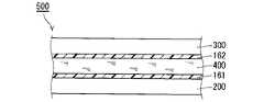
図1は、本実施の形態における液晶表示装置500の構成を概略的に示す部分断面図である。液晶表示装置500は、TFT基板200(薄膜トランジスタ基板)と、カラーフィルタ基板300(対向基板)と、液晶層400と、配向層161と、配向層162とを有している。カラーフィルタ基板300は、TFT基板200と間隔を空けて配置されている。液晶層400はTFT基板200およびカラーフィルタ基板300の間に保持されている。配向層161および162の各々は、液晶層400を配向させるものである。配向層161および162のそれぞれは、TFT基板200およびカラーフィルタ基板300上に設けられている。本実施の形態においては、液晶表示装置500はFFSモードのものである。<Embodiment 1>
(Configuration of liquid crystal display device)
FIG. 1 is a partial cross-sectional view schematically showing a configuration of a liquid
(TFT基板の構成)
図2は、TFT基板200の構成を模式的に示す平面図である。TFT基板200は、画像を表示する表示領域101と、表示領域101の外に設けられた額縁領域102とを有している。額縁領域102は、典型的には、図2に示されているように、表示領域101を囲んでいる。配向層161および162(図1)の各々は、平面視において、少なくとも表示領域101を包含するように配置されている。(Configuration of TFT substrate)
FIG. 2 is a plan view schematically showing the configuration of the
TFT基板200は、額縁領域102において、複数の外部配線107と、複数の端子電極108と、複数のIC(Integrated Circuit)チップ109とを有している。なお、図2では、便宜上、一つの端子電極108のみを図示している。外部配線107は、表示領域101の信号線103(ソース配線)および走査線104(ゲート配線)の各々から額縁領域102まで延びている配線である。端子電極108は、外部配線107の端部と電気的に接続されており、端子電極108の幅よりも大きな幅を有している。端子電極108は、外部接続用の端子であり、ここではICチップ109およびプリント基板110などの外部部材と重なるように配置されている。これにより、外部部材が外部配線107に電気的に接続されている。ICチップ109の端子は、端子電極108と、バンプまたはACF(Anisotropic Conductive Film)を介して電気的に接続されている。同じように、プリント基板110の端子は、端子電極108とバンプまたはACFを介して電気的に接続されている。 The
表示領域101には、複数の信号線103と、複数の走査線104と、これらと電気的に接続された複数のTFT105と、共通配線106とが設けられている。複数の信号線103および複数の走査線104は、互いに直交するように配設されている。隣接する信号線103と、隣接する走査線104とが囲む領域の各々には、1つの画素PX1が構成されている。これにより、複数の画素PX1がマトリックス状に配置されている。複数の画素PX1の各々にはTFT105が設けられている。よって複数のTFT105がマトリックス状に配列されている。 In the
(画素の構成および機能)
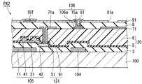
図3は、各画素PX1の構成を概略的に示す部分平面図である。図4は、図3と同様の視野での図であり、各画素PX2の構成を、一部の部材の図示を省略しつつ概略的に示す部分平面図である。図5は、線V−V(図3および図4)に沿う概略部分断面図である。なお、図を見やすくするために、図4において金属層15にドット模様が付されている。(Pixel configuration and function)
FIG. 3 is a partial plan view schematically showing the configuration of each pixel PX1. FIG. 4 is a view with the same field of view as FIG. 3, and is a partial plan view schematically showing the configuration of each pixel PX <b> 2 while omitting illustration of some members. FIG. 5 is a schematic partial sectional view taken along line VV (FIGS. 3 and 4). In addition, in order to make a figure legible, the dot pattern is attached | subjected to the
TFT基板200は、透明絶縁性基板100(支持基板)と、走査線104と、ゲート絶縁膜2と、チャネル層31と、信号線103と、ドレイン電極42と、絶縁膜20(第1の絶縁膜)と、画素電極71と、層間絶縁膜8(第2の絶縁膜)と、共通電極91と、金属層15とを有している。 The
走査線104は透明絶縁性基板100上に設けられている。画素PX1の各々において走査線104の一部の領域はゲート電極11としての機能を有している。言い換えれば、走査線104は、画素PX1の各々に配置されたゲート電極11を含む。 The
ゲート絶縁膜2は走査線104を覆っている。ゲート絶縁膜2としては、例えばSiN膜もしくはSiO膜またはSiOとSiNとの積層膜などが用いられる。 The
チャネル層31は、ゲート絶縁膜2を介してゲート電極11の各々の上に、島状に設けられている。チャネル層31は酸化物半導体からなる。酸化物半導体は、一般に、光によって劣化しやすい。 The
ゲート電極11は、典型程にはAl、Cu、Ni、Ag、Nd、Mo、Nbなどの金属材料からなるので、遮光性を有している。この遮光性により、液晶表示装置500(図1)の動作時に、図1の下側からのバックライトの光がチャネル層31へ入射することが抑制される。この効果を高めるためには、チャネル層31が平面視においてゲート電極11に包含されていることが好ましい。 Since the
信号線103(図4)はゲート絶縁膜2(図5)上に設けられている。画素PX1の各々において信号線103の一部の領域はソース電極41としての機能を有している。言い換えれば、信号線103は、画素PX1の各々に配置されたソース電極41を含む。ソース電極41はチャネル層31の一方端部上に接している。 The signal line 103 (FIG. 4) is provided on the gate insulating film 2 (FIG. 5). In each pixel PX 1, a part of the
ドレイン電極42は画素PX1の各々に配置されている。ドレイン電極42は、チャネル層31の他方端部上に接しており、ソース電極41から離れている。チャネル層31のうちソース電極41とドレイン電極42との間の部分が、TFT105のチャネル領域として機能する。 The
絶縁膜20は、表示領域101(図2)および額縁領域102(図2)に跨って設けられている。表示領域101において、絶縁膜20はチャネル層31と信号線103とドレイン電極42との上に設けられている。絶縁膜20には、ドレイン電極42に達するドレインコンタクトホール121が設けられている。 The insulating
絶縁膜20は、保護絶縁膜5と、その上に積層された平坦化膜6とを有している。保護絶縁膜5および平坦化膜6のそれぞれにはコンタクトホール51およびコンタクトホール61が設けられている。これらが互いにつながることで、上述したドレインコンタクトホール121が構成されている。額縁領域102において、絶縁膜20は、外部配線107上に設けられている。絶縁膜20と外部配線107との間にゲート絶縁膜2が延びていてもよい。 The insulating
保護絶縁膜5としては、例えば、SiN膜もしくは酸化シリコン膜(SiO膜)、またはSiNとSiOの積層膜などの無機絶縁膜が用いられる。保護絶縁膜5にSiN膜などの無機絶縁膜を用いることで、平坦化膜6などからの水分などによりTFT105の特性が劣化することを抑制することができる。それでだけでなく、無機絶縁膜は高い機械強度を有することから、外部からの傷が生じ難いという効果も得られる。 As the protective
平坦化膜6はTFT105上に保護絶縁膜5を介して配置されている。平坦化膜6は、平坦化された上面を有している。平坦化膜6としては、例えば有機樹脂膜が用いられてもよい。有機樹脂は、優れた平坦性を有するので、平坦化膜6の材料に有機樹脂が適用された場合には、平坦化膜6下方のTFT105などの構造物の段差(高低差)が、平坦化膜6の上面に反映され難くなる。これにより、画素電極71ひいては共通電極91を平坦な平面上に形成することができる。 The
平坦化膜6としては、例えば、アクリルを主体とした有機樹脂膜、またはスピンオングラス(Spin On Glass:SOG)膜が用いられてもよい。これらの比誘電率は3〜4程度であり、SiNの比誘電率(6〜7)などと比べて低い。このため、平坦化膜6にアクリル樹脂またはSOG膜が適用された場合には、信号線103と下部電極(画素電極71)との間の寄生容量が小さくなる。これにより、信号線103から画素電極71へのノイズの影響を抑制することができる。よって、ノイズに起因した表示品位の悪化を抑制することができる。なお、ノイズの影響を抑制するという点だけをみれば、平坦化膜6に、SOG膜の誘電率と同程度の誘電率を有するSiO膜を適用することも考えられる。ただし、SiO膜は、SiN膜と同様、平坦化がやや困難である。 As the
平坦化膜6の材料には、例えば、感光性を有する材料から形成された有機樹脂膜が用いられてもよい。その場合、フォトリソグラフィーによって、平坦化膜6に所望のパターンを有する開口を形成することができる。よって、コンタクトホール61を、エッチングを行うことなく容易に形成することができる。そして、コンタクトホール61が設けられた平坦化膜6をエッチングマスクとして用いたドライエッチングにより、保護絶縁膜5にコンタクトホール51を形成することができる。 For example, an organic resin film formed of a photosensitive material may be used as the material of the
画素電極71は絶縁膜20の平坦化膜6上に設けられている。画素電極71は、画素PX1の各々に配置されたパターンを有している。画素電極71は透明導電材料からなる。透明導電材料としては、例えば、IZO(Indium Zinc Oxide)またはITO(Indium Tin Oxide)などが用いられる。画素電極71は、平板電極部分に加えて、接続導電層71aを有している。接続導電層71aはドレインコンタクトホール121によってドレイン電極42に電気的に接続されている。接続導電層71aが設けられることにより、画素電極71はドレイン電極42に電気的に接続されている。図5においては画素電極71の平板電極部分と接続導電層71aとが分離されているように見えるが、図4に示すように、両者は互いにつながっている。 The
層間絶縁膜8は画素電極71上に設けられている。層間絶縁膜8は画素電極71を覆っている。 The
共通電極91は層間絶縁膜8上に設けられている。共通電極91は透明導電材料からなる。透明導電材料としては、例えば、IZOまたはITOなどが用いられる。共通電極91は、平面視において画素電極71と部分的に重畳している。画素PX1の各々において共通電極91はスリット91a(開口部)を有している。スリット91aは厚み方向において層間絶縁膜8を介して画素電極71と対向している。下部電極としての画素電極71と、上部電極としての共通電極91との間に電圧を印加すると、両電極間でフリンジ電界が発生する。フリンジ電界は、画素電極71から出て、共通電極91のスリット91aの開口部を介して上方に進み、共通電極91の上方に配設された液晶層400(図1)内にて水平方向(横方向)に向かってから、下側に位置する共通電極91に向かう。このようにフリンジ電界は、透明絶縁性基板100とほぼ水平な電界を含む。この水平な電界によって液晶層400内の液晶分子が水平方向に駆動される。これにより、当該液晶分子を通過する光の偏光方向が画素ごとに適宜変更される。よって、表示領域101(図2)において、画素PX1を単位とした所望の表示を行うことが可能となる。 The
なお、共通電極91(図3)と画素電極71(図4)とが重畳された領域が、画素PX1を単位とした表示に用いられる領域、つまり画素表示領域151(図3)、である。カラーフィルタ基板300(図1)が有する遮光膜(ブラックマトリックス)は、平面視において、画素表示領域151に対応する領域に開口部を有する。また、共通電極91は複数の画素PX1に跨っていることで、共通配線106(図2)としての機能も有している。 Note that a region where the common electrode 91 (FIG. 3) and the pixel electrode 71 (FIG. 4) are overlapped is a region used for display in units of the pixel PX1, that is, the pixel display region 151 (FIG. 3). The light shielding film (black matrix) included in the color filter substrate 300 (FIG. 1) has an opening in a region corresponding to the
ゲート電極11とゲート絶縁膜2とチャネル層31とソース電極41とドレイン電極42とにより、画素電極71および共通電極91の下方において透明絶縁性基板100上に、TFT105が構成されている。走査線104からゲート電極11に供給される電圧により、TFT105のオンとオフとが制御される。また、外部から入力された信号データに基づいて信号線103からソース電極41に電圧が供給される。この構成により、信号線103から供給される信号データに基づいた電圧を、特定の画素PX1のドレイン電極42に選択的に印加することができる。ドレイン電極42に接続された画素電極71には、電流(信号データ)が伝達される。信号データは、端子電極108(図2)に接続されたICチップ109およびプリント基板110によって制御される。この制御は、外部から入力された表示データに基づいて行われる。以上により、複数の画素PX1の各々の表示が、外部から入力された表示データに基づいて制御される。 The
金属層15は、共通電極91の一部と積層構造を有している。図5に示された例においては、金属層15は層間絶縁膜8上に設けられている。金属層15は、金属材料からなり、ここでいう「金属材料」は合金材料であってもよい。金属材料は、一般に、高い遮光性を有している。 The
金属層15は遮光部15fを有している。遮光部15fは、平面視において、チャネル層31と少なくとも部分的に重なっており、好ましくは、図4に示すようにチャネル層31を包含している。遮光部15fにより、チャネル層31の上方から入射する光を遮光することができる。よって、酸化物半導体層からなるTFT105の電気特性の変化を防ぐことができる。チャネル層31へ向かう上方からの光としては、製造時に用いられる照射光、または、液晶表示装置500としての動作時の回り込み光などがある。製造時に用いられる光としては、例えば、TFT基板200の洗浄工程において照射されるUV(ultraviolet:紫外)光がある。 The
平坦化膜6として、有機樹脂膜、特に、感光性を有する有機樹脂から形成された有機樹脂膜、が用いられる場合は、平坦化膜6が可視光の短波長側およびUV光を吸収しやすい。このような平坦化膜6は、チャネル層31への光入射を、ある程度抑制する。しかしながら、より十分な抑制のためには遮光部15fが必要である。平坦化膜6としてSOG膜が用いられる場合は、有機樹脂膜が用いられる場合と異なり、可視光の短波調側およびUV光が平坦化膜6を透過しやすい。このため、遮光部15fなしでは、酸化物半導体層を用いたTFT105の電気特性が大きく変化しやすい。よって、遮光部15fによる大きな効果が得られる。 When an organic resin film, in particular, an organic resin film formed from a photosensitive organic resin, is used as the
金属層15は共通電極91と接触している。これにより、共通電極91に加えて金属層15も共通配線106(図1)を構成する。よって共通配線106の電気抵抗を低くすることができる。金属層15が走査線104に沿って延びている場合、共通配線106の電気抵抗を顕著に低くすることができる。これにより、共通配線106の異なる箇所間での、電圧降下に起因した電位差を低くすることができる。よって、この電位差に起因しての、共通電極91と画素電極71との間の電圧の変動が抑制される。よって、共通電極91と画素電極71との間の電圧に応じて生じるフリンジ電界の、異なる画素PX1間でのばらつきが抑制される。よって、液晶表示装置500の表示むらを抑えることができる。また、共通配線106の電気抵抗を低くすることで、信号遅延に起因した表示むらも抑えることができる。金属層15の材料としては、低い抵抗率を有するものが好ましく、例えば、Al、Ni、Mo、Nb、Ag、Nd、Cuなどの金属材料、または、それらの複数の金属材料を含む金属合金が用いられる。 The
金属層15は、平面視において、走査線104と、少なくとも部分的に重なっている。これにより、表示領域101(図1)中の画素表示領域151(図3)の割合、すなわち開口率、を高く保ちつつ、金属層15のための面積を大きく確保することができる。 The
金属層15の上述した機能のみを考慮すれば、金属層15は、共通電極91の上面および下面のいずれに配置されてもよい。しかしながら、金属層15が共通電極91の上面上に設けられると、金属層15が液晶層400(図1)に、より近く配置される。このため、液晶層400と金属層15との接触の可能性が高まる。液晶層400に異種の金属が接触すると、接触電位差に起因して液晶層400に直流電圧が印加される。この結果、液晶層400に液晶材料の組成変質などの悪影響が生じることがある。このような現象を防ぐためには、金属層15は、共通電極91の上面ではなく下面に配置されることが好ましい。言い換えれば、金属層15は、層間絶縁膜8と共通電極91との間に配置されることが好ましい。 Considering only the above-described function of the
(効果のまとめ)
本実施の形態によれば、図5に示されているように、共通電極91は画素電極71の上方に配置される。これにより、厚み方向において、TFT105と、透明導電材料からなる画素電極71との間に、共通電極91が配置されなくてよい。よって、これらの間に共通電極91が配置される場合に比して、TFT105と画素電極71との間の電気的経路を短くし得る。よって、その電気抵抗が過度に大きくなることを避けつつ、当該電気的経路を構成するコンタクトホールの面積を抑えることができる。よって、非画素表示領域の面積を抑えることができる。よって、大きな開口率を確保しやすくなる。さらに、第1に、チャネル層31への光を遮る遮光部15fを有する金属層15が設けられる。これにより、酸化物半導体からなるチャネル層31の、光に起因した劣化が抑制される。よって、チャネル層31の劣化に起因しての表示制御の不良が抑制される。第2に、金属層15は共通電極91の一部と積層構造を有している。この積層構造は、低抵抗の電気的経路を構成する。これにより、TFT基板200内での共通電極91の電位の差異が抑制される。よって、TFT基板200を用いた表示装置の表示むらが抑制される。以上から、大きな開口率を確保しつつ、表示不良を抑制することができる。(Summary of effects)
According to the present embodiment, the
好ましくは、金属層15は、図4における横方向に沿って、すなわち走査線104に沿って、延びている。これにより、走査線104の延在方向、言い換えればTFT基板200(図2)の行方向、に沿った、共通電極91による電流経路の電気抵抗を、大幅に低減することができる。よって、行方向における複数の画素PX1間での表示むらが抑制される。 Preferably, the
好ましくは、図4に示されているように、チャネル層31は平面視においてゲート電極11に包含されている。これにより、透明絶縁性基板100からチャネル層31へ向かう光がゲート電極11によって十分に遮られる。よって、光に起因した酸化物半導体の劣化が抑制される。よって、酸化物半導体からなるチャネル層31の劣化に起因しての表示制御の不良が、より抑制される。 Preferably, as shown in FIG. 4, the
好ましくは、図5に示されているように、金属層15は層間絶縁膜8と共通電極91との間に配置されている。これにより、金属層15が液晶層400(図1)からより遠ざけられる。よって、金属層15と液晶層400との間の接触電位差が液晶層400へ及ぼす悪影響を防止することができる。 Preferably, as shown in FIG. 5, the
絶縁膜20は有機樹脂膜を含み得る。これにより、絶縁膜20の表面の平坦性を容易に高めることができる。また、比較的低い誘電率を有する有機樹脂膜によって画素電極71と信号線103とが互いに絶縁されることで、両者の間の寄生容量が小さくなる。これにより、信号線103から画素電極71へのノイズに起因しての表示品位の悪化を抑制することができる。 The insulating
絶縁膜20はSOG膜を含み得る。これにより、絶縁膜20の表面の平坦性を容易に高めることができる。また、比較的低い誘電率を有する有機樹脂膜によって画素電極71と信号線103とが互いに絶縁されることで、両者の間の寄生容量が小さくなる。これにより、信号線103から画素電極71へのノイズに起因しての表示品位の悪化を抑制することができる。 The insulating
<実施の形態2>
図6および図7を参照して、本実施の形態においては、TFT基板200(図1および図2)は、実施の形態1で説明した画素PX1(図4および図5)に代わり、画素PX2を有している。<
Referring to FIGS. 6 and 7, in the present embodiment, TFT substrate 200 (FIGS. 1 and 2) is replaced with pixel PX2 instead of pixel PX1 (FIGS. 4 and 5) described in the first embodiment. have.
画素PX2において、TFT基板200は、共通透明導電層106aを有している。共通透明導電層106aは絶縁膜20上に配置されている。言い換えれば、共通透明導電層106aは、画素電極71と同層に配置されている。共通透明導電層106aは画素電極71から離れて設けられている。共通透明導電層106aは透明導電材料からなる。好ましくは、共通透明導電層106aは、画素電極71の材料と同じ材料からなり、この場合、両者を同時に形成することが可能である。これにより、工程数を増やすことなく共通透明導電層106aを形成することができる。 In the pixel PX2, the
層間絶縁膜8には、共通透明導電層106aに達する共通透明導電層コンタクトホール81が設けられている。金属層15は、接続金属層15aを有している。接続金属層15aは共通透明導電層コンタクトホール81によって共通透明導電層106aに電気的に接続されている。よって本実施の形態においては、共通配線106が、共通電極91および金属層15だけでなく共通透明導電層106aによっても構成されている。これにより、共通配線106の電気抵抗を下げることができる。これにより、TFT基板200内での共通電極91の電位の差異が、より抑制される。よって、TFT基板200を用いた表示装置の表示むらが、より抑制される。 The
共通透明導電層106aは、平面視において、走査線104に、少なくとも部分的に重なっていることが好ましい。これにより、表示領域101(図1)中の画素表示領域151(図3)の割合、すなわち開口率、を高く保ちつつ、共通透明導電層106aのための面積を大きく確保することができる。 The common transparent
共通透明導電層106aが、平面視においてチャネル層31と、少なくとも部分的に重なっている場合、厚み方向において共通透明導電層106aとゲート電極11との間にチャネル層31が挟まれる。この場合に共通透明導電層106aとゲート電極11との間に電位差が生じると、チャネル層31に、厚み方向(図7における縦方向)の電界が加わる。この電界が大きいとチャネル層31が劣化し得る。特に、共通透明導電層106a上において層間絶縁膜8に共通透明導電層コンタクトホール81がドライエッチングによって形成される際に、チャネル層31に大きな電界が印加されやすい。よって、このドライエッチング時にチャネル層31が特に劣化しやすい。チャネル層31のこのような劣化を避けるため、共通透明導電層106aは、平面視においてチャネル層31の外に配置されることが好ましい。 When the common transparent
なお、上記以外の構成については、上述した実施の形態1の構成とほぼ同じであるため、同一または対応する要素について同一の符号を付し、その説明を繰り返さない。 Since the configuration other than the above is substantially the same as the configuration of the first embodiment described above, the same or corresponding elements are denoted by the same reference numerals, and description thereof is not repeated.
<実施の形態3>
(構成)
図8および図9を参照して、本実施の形態においては、TFT基板200(図1および図2)は、実施の形態1で説明した画素PX1(図4および図5)に代わり、画素PX3を有している。<
(Constitution)
Referring to FIGS. 8 and 9, in the present embodiment, TFT substrate 200 (FIGS. 1 and 2) is replaced with pixel PX3 instead of pixel PX1 (FIGS. 4 and 5) described in the first embodiment. have.
画素PX3において、ゲート絶縁膜2には、走査線104に達する下部ゲートコンタクトホール53(第1のゲートコンタクトホール)が設けられている。絶縁膜20には、下部ゲートコンタクトホール53につながれた上部ゲートコンタクトホール122(第2のゲートコンタクトホール)が設けられている。上部ゲートコンタクトホール122は、保護絶縁膜5および平坦化膜6のそれぞれに設けられたコンタクトホール52およびコンタクトホール62によって構成されている。 In the pixel PX3, the
金属層15は、本実施の形態においては、図9に示すように、絶縁膜20の平坦化膜6上に部分的に設けられている。言い換えれば、金属層15は、画素電極71と同層に配置されている。層間絶縁膜8は画素電極71および金属層15を覆っている。なお、金属層15に含まれる遮光部15fの平面視における配置は実施の形態1と同様である。 In the present embodiment, the
金属層15は接続金属層15aを有している。接続金属層15aは、下部ゲートコンタクトホール53および上部ゲートコンタクトホール122を通って走査線104に達している。言い換えれば、金属層15は、下部ゲートコンタクトホール53および上部ゲートコンタクトホール122によって走査線104に電気的に接続されている。 The
なお、上記以外の構成については、上述した実施の形態1の構成とほぼ同じであるため、同一または対応する要素について同一の符号を付し、その説明を繰り返さない。 Since the configuration other than the above is substantially the same as the configuration of the first embodiment described above, the same or corresponding elements are denoted by the same reference numerals, and description thereof is not repeated.
(効果)
実施の形態1と同様、本実施の形態においても、厚み方向において、TFT105と、透明導電材料からなる画素電極71との間に、共通電極91が配置されなくてよい。これにより、これらの間に共通電極91が配置される場合に比して、TFT105と画素電極71との間の電気的経路を短くし得る。よって、その電気抵抗が過度に大きくなることを避けつつ、当該電気的経路を構成するコンタクトホールの面積を抑えることができる。よって、非画素表示領域の面積を抑えることができる。よって、大きな開口率を確保しやすくなる。さらに、チャネル層31への光を遮る遮光部15fを有する金属層15が設けられる。これにより、酸化物半導体からなるチャネル層31の、光に起因した劣化が抑制される。よって、チャネル層31の劣化に起因しての表示制御の不良が抑制される。以上から、大きな開口率を確保しつつ、表示不良を抑制することができる。(effect)
Similar to the first embodiment, in this embodiment, the
さらに本実施の形態によれば、金属層15は、走査線104に電気的に接続されている。すなわち、金属層15と走査線104とが互いに電気的に短絡されている。これにより、金属層15に含まれる遮光部15fと、走査線104に含まれるゲート電極11との間での高電界の発生が避けられる。よって、遮光部15fとゲート電極11との間に配置されたチャネル層31が高電界に起因して劣化することが防止される。よって、チャネル層31の劣化に起因しての表示制御の不良がより抑制される。仮に、金属層15がゲート電極11に電気的に接続されていないとすると、金属層15とゲート電極11との間に、TFT基板200の製造時または使用時における何らかの要因により電位差が発生し得る。この場合、金属層15の遮光部15fとゲート電極11との間に配置されたチャネル層31に、厚み方向(図9における縦方向)の電界が加わる。この電界が大きいとチャネル層31が劣化し得る。 Furthermore, according to the present embodiment, the
好ましくは、金属層15は走査線104に沿って延びている。これにより、走査線104の延在方向、言い換えれば行方向、に沿った、走査線104による電流経路の電気抵抗を低減することができる。よって、TFT基板200内での各走査線104の電位差、および、走査線104の信号遅延が抑制される。よって、行方向における複数の画素PX3間での表示むらが抑制される。 Preferably, the
(変形例)
上記本実施の形態においては、図8および図9に示すように、画素電極71と金属層15とが互いに重ならないように配置されている。(Modification)
In the present embodiment, as shown in FIGS. 8 and 9, the
第1の変形例として、金属層15は、接続金属層15aに加えて、接続導電層71aと積層された接続金属層を含んでもよい。これにより、ドレイン電極42へのコンタクト抵抗が低減される。よって、表示特性をより向上させることができる。なお、走査線104と画素電極71との短絡を避けるため、追加される接続金属層が接続金属層15aからは分離されている必要がある。 As a first modification, the
第2の変形例として、画素電極71の材料と同じ透明導電材料からなり接続金属層15aと積層された接続導電層が設けられてもよい。これにより、走査線104へのコンタクト抵抗が低減される。よって、表示特性をより向上させることができる。なお、走査線104と画素電極71との短絡を避けるためには、追加される接続導電層が画素電極71からは分離されている必要がある。この変形例に上記第1の変形例が組み合わされてもよい。 As a second modification, a connection conductive layer made of the same transparent conductive material as the material of the
<実施の形態4>
本実施の形態においては、配向層161(図1)は、光配向性を有する材料からなる。この場合、液晶表示装置500の製造方法は、光配向性を有する材料からなる配向層161をTFT基板200上に形成する工程と、この配向層161に対して光配向処理を行う工程とを有する。光配向処理により、配向層161の表面の配向状態が所望のものに変化させられる。光配向処理は、例えば、TFT基板200の上面に配向層161を形成した後、上方向または斜め上方向からUV光を照射することにより行われる。なお、上記以外の構成については、上述した実施の形態1〜3の構成とほぼ同じである。<Embodiment 4>
In the present embodiment, the alignment layer 161 (FIG. 1) is made of a material having photo-alignment properties. In this case, the method for manufacturing the liquid
本実施の形態によれば、光配向処理において、チャネル層31へ向かう光が遮光部15fによって遮られる。これにより、遮光部15fがない場合に比して、酸化物半導体からなるチャネル層31の光に起因した劣化が抑制される。よって、チャネル層31の劣化に起因しての表示制御の不良が抑制される。 According to the present embodiment, in the photo-alignment process, the light traveling toward the
<実施の形態5>
(構成)
図10を参照して、外部配線107(図2)は、典型的には、外部ゲート配線107a(第1の配線)と、外部ソース配線107b(第2の配線)とを含む。外部ゲート配線107aは、透明絶縁性基板100上に配置されている。言い換えれば、外部ゲート配線107aは、走査線104と同層に配置されている。外部ゲート配線107aは、走査線104の材料と同じ材料からなる。よって外部ゲート配線107aは、走査線104と同時に形成され得る。外部ソース配線107bは、ゲート絶縁膜2上に配置されている。言い換えれば、外部ソース配線107bは、信号線103と同層に配置されている。外部ソース配線107bは信号線103の材料と同じ材料からなる。よって外部ソース配線107bは、信号線103と同時に形成され得る。外部配線107の構成上、外部ゲート配線107aと外部ソース配線107bとが額縁領域102(図2)において互いに電気的に接続される場合がある。本実施の形態は、このような場合について説明する。<
(Constitution)
Referring to FIG. 10, external wiring 107 (FIG. 2) typically includes an
本実施の形態においては、額縁領域102において、ゲート絶縁膜2にはコンタクトホール55が設けられており、保護絶縁膜5にはコンタクトホール54およびコンタクトホール56が設けられており、平坦化膜6にはコンタクトホール64およびコンタクトホール66が設けられている。コンタクトホール64とコンタクトホール54とコンタクトホール55とがつながることによって、絶縁膜20およびゲート絶縁膜2を貫通する外部ゲートコンタクトホール124(第1のコンタクトホール)が構成されている。コンタクトホール66とコンタクトホール56とがつながることによって、絶縁膜20を貫通する外部ソースコンタクトホール126(第2のコンタクトホール)が構成されている。 In the present embodiment, in the
金属層15は、額縁領域102内に配置された接続金属層15pを含む。接続金属層15pは、外部ゲートコンタクトホール124によって外部ゲート配線107aに電気的に接続されており、かつ、外部ソースコンタクトホール126によって外部ソース配線107bに電気的に接続されている。これにより、外部ゲート配線107aと外部ソース配線107bとが互いに電気的に接続されている。金属層15は、本実施の形態においては、実施の形態1または2と同様、層間絶縁膜8上に配置されている。このため層間絶縁膜8には、外部ゲートコンタクトホール124および外部ソースコンタクトホール126のそれぞれにつながるコンタクトホール82およびコンタクトホール83が設けられている。 The
額縁領域102には、接続導電層71pが設けられてもよい。接続導電層71pは、絶縁膜20上に配置されている。言い換えれば、接続導電層71pは、画素電極71(図5または図7)と同層に配置されている。また接続導電層71pは、画素電極71の透明導電材料と同じものから形成され得る。よって接続導電層71pは、画素電極71と同時に形成され得る。接続導電層71pが接続金属層15pと外部ゲートコンタクトホール124において積層されることで、そのコンタクト抵抗を低減することができる。接続導電層71pが接続金属層15pと外部ソースコンタクトホール126において積層されることで、そのコンタクト抵抗を低減することができる。接続導電層71pのうち外部ゲートコンタクトホール124に配置された部分と外部ソースコンタクトホール126に配置された部分とは、必ずしも互いにつながっている必要はないが、図示されているように互いにつながっている場合、外部ゲート配線107aと外部ソース配線107bとの間の電気抵抗をより低減することができる。 In the
額縁領域102には、接続導電層91pが設けられてもよい。接続導電層91pは、層間絶縁膜8上に配置されており、図10においては、接続金属層15pが設けられた層間絶縁膜8上に配置されている。言い換えれば、接続導電層91pは、共通電極91(図5または図7)と同層に配置されている。また接続導電層91pは、共通電極91の透明導電材料と同じものから形成され得る。よって接続導電層91pは、共通電極91と同時に形成され得る。接続導電層91pが接続金属層15pと外部ゲートコンタクトホール124およびコンタクトホール82において積層されることで、そのコンタクト抵抗を低減することができる。接続導電層91pが接続金属層15pと外部ソースコンタクトホール126およびコンタクトホール83において積層されることで、そのコンタクト抵抗を低減することができる。接続導電層91pのうち外部ゲートコンタクトホール124に配置された部分と外部ソースコンタクトホール126に配置された部分とは、必ずしも互いにつながっている必要はないが、図示されているように互いにつながっている場合、外部ゲート配線107aと外部ソース配線107bとの間の電気抵抗をより低減することができる。 In the
なお上記以外の構成については、上述した実施の形態1または2の構成とほぼ同じであるため、同一または対応する要素について同一の符号を付し、その説明を繰り返さない。 Since the configuration other than the above is substantially the same as the configuration of the first or second embodiment described above, the same or corresponding elements are denoted by the same reference numerals, and description thereof will not be repeated.
(効果)
本実施の形態によれば、外部ゲート配線107aと外部ソース配線107bとの間が接続金属層15pによって接続される。接続金属層15pは、透明導電材料の抵抗率に比して一般に低い抵抗率を有する材料である金属からなる。これにより、外部ゲート配線107aと外部ソース配線107bとの間を低抵抗で接続することができる。よって、外部ゲート配線107aと外部ソース配線107bとを有する外部配線107の配線抵抗および信号遅延を小さくし得る。言い換えれば、表示領域101へ至る外部配線107の配線抵抗および信号遅延を小さくし得る。よって表示特性を向上させることができる。(effect)
According to the present embodiment, the
なお額縁領域102(図2)に配置される接続金属層15pは、金属層15の他の部分と同時に形成され得る。よって、接続金属層15pを設けることによる工程数の増加は避けることができる。 The
(第1の変形例)
外部配線107(図2)と同様の機能を有する構成の少なくとも一部が、表示領域101内に分散配置されてもよい。このような配置は、例えば、表示領域101内に駆動回路が分散配置される場合に適用される。この場合、上述した接続金属層15pは、額縁領域102に代わりまたはそれに加えて表示領域101内に配置され得る。(First modification)
At least a part of the configuration having the same function as that of the external wiring 107 (FIG. 2) may be distributed in the
(第2の変形例)
上記の本実施の形態においては、接続金属層15p(図10)が実施の形態1または2(図5または図7)の構成に適用される場合について説明した。一方、本変形例の接続金属層15p(図11)は、実施の形態3(図9)の構成に適用されるものである。この場合、金属層15の接続金属層15p(図11)は、接続金属層15aおよび遮光部15f(図9)と共に、絶縁膜20の平坦化膜6上に配置される。よって、接続金属層15pの配置に関する限り、層間絶縁膜8のコンタクトホール82およびコンタクトホール83は、必ずしも必要ではない。ただしこれらのコンタクトホールは、接続導電層91pが設けられる場合に必要となる。(Second modification)
In the present embodiment, the case where the
(第3の変形例)
TFT105の製造工程と同様の工程を用いて、ICチップ109(図2)の機能を有する電子回路を額縁領域102に形成し得る。この電子回路内の配線として、外部ゲート配線107aおよび外部ソース配線107bが用いられ得る。これにより、当該電子回路内の配線抵抗および信号遅延が低減される。よって表示特性を向上させることができる。(Third Modification)
An electronic circuit having the function of the IC chip 109 (FIG. 2) can be formed in the
上記各実施の形態においては、液晶の駆動方式として一般的なFFSモードが用いられる場合について詳しく説明したが、一般的なFFSモード以外の他のモードが用いられてもよい。またTFT基板が適用される表示装置として液晶表示装置について詳しく説明したが、TFT基板が液晶表示装置以外の他の表示装置に適用されてもよい。 In each of the above embodiments, the case where a general FFS mode is used as a liquid crystal driving method has been described in detail, but other modes than the general FFS mode may be used. Although the liquid crystal display device has been described in detail as a display device to which the TFT substrate is applied, the TFT substrate may be applied to other display devices other than the liquid crystal display device.
本発明は、その発明の範囲内において、各実施の形態を自由に組み合わせたり、各実施の形態を適宜、変形、省略したりすることが可能である。 Within the scope of the present invention, the present invention can be freely combined with each other, or can be appropriately modified or omitted.
PX1〜PX3 画素、2 ゲート絶縁膜、5 保護絶縁膜、6 平坦化膜、8 層間絶縁膜(第2の絶縁膜)、11 ゲート電極、15a,15p 接続金属層、15 金属層、15f 遮光部、20 絶縁膜(第1の絶縁膜)、31 チャネル層、41 ソース電極、42 ドレイン電極、51,52,54〜56,61,62,64,66,82,83 コンタクトホール、53 下部ゲートコンタクトホール(第1のゲートコンタクトホール)、71 画素電極、71a,71p,91p 接続導電層、81 共通透明導電層コンタクトホール、91 共通電極、91a スリット(開口部)、100 透明絶縁性基板、101 表示領域、102 額縁領域、103 信号線(ソース配線)、104 走査線(ゲート配線)、105 TFT、106 共通配線、106a 共通透明導電層、107 外部配線、107a 外部ゲート配線(第1の配線)、107b 外部ソース配線(第2の配線)、121 ドレインコンタクトホール、122 上部ゲートコンタクトホール(第2のゲートコンタクトホール)、124 外部ゲートコンタクトホール(第1のコンタクトホール)、126 外部ソースコンタクトホール(第2のコンタクトホール)、151 画素表示領域、161,162 配向層、200 TFT基板(薄膜トランジスタ基板)、300 カラーフィルタ基板(対向基板)、400 液晶層、500 液晶表示装置。 PX1 to PX3 pixel, 2 gate insulating film, 5 protective insulating film, 6 planarizing film, 8 interlayer insulating film (second insulating film), 11 gate electrode, 15a, 15p connecting metal layer, 15 metal layer, 15f light shielding portion , 20 Insulating film (first insulating film), 31 Channel layer, 41 Source electrode, 42 Drain electrode, 51, 52, 54 to 56, 61, 62, 64, 66, 82, 83 Contact hole, 53 Lower gate contact Hole (first gate contact hole), 71 pixel electrode, 71a, 71p, 91p connection conductive layer, 81 common transparent conductive layer contact hole, 91 common electrode, 91a slit (opening), 100 transparent insulating substrate, 101 display Area, 102 frame area, 103 signal line (source wiring), 104 scanning line (gate wiring), 105 TFT, 106 Common wiring 106a common transparent conductive layer 107 external wiring 107a external gate wiring (first wiring) 107b external source wiring (second wiring) 121 drain contact hole 122 upper gate contact hole (second gate) Contact hole), 124 external gate contact hole (first contact hole), 126 external source contact hole (second contact hole), 151 pixel display region, 161, 162 alignment layer, 200 TFT substrate (thin film transistor substrate), 300 Color filter substrate (counter substrate), 400 liquid crystal layer, 500 liquid crystal display device.
Claims (13)
Translated fromJapanese支持基板と、
前記支持基板上に設けられ、前記画素の各々に配置されたゲート電極を含むゲート配線と、
前記ゲート配線を覆うゲート絶縁膜と、
前記ゲート絶縁膜を介して前記ゲート電極の各々の上に設けられ、酸化物半導体からなるチャネル層と、
前記画素の各々に配置されかつ前記チャネル層に接するソース電極を含むソース配線と、
前記画素の各々に配置され、前記チャネル層に接し、前記ソース電極から離れたドレイン電極と、
前記チャネル層と前記ソース配線と前記ドレイン電極との上に設けられ、前記ドレイン電極に達するドレインコンタクトホールが設けられた第1の絶縁膜と、
前記画素の各々において前記第1の絶縁膜上に設けられ、前記ドレインコンタクトホールによって前記ドレイン電極に電気的に接続された接続導電層を含み、透明導電材料からなる画素電極と、
前記画素電極を覆う第2の絶縁膜と、
前記第2の絶縁膜上に設けられ、厚み方向において前記画素電極と対向する開口部を有し、透明導電材料からなる共通電極と、
前記共通電極の一部と積層構造を有し、平面視において前記チャネル層と少なくとも部分的に重なる遮光部を有する金属層と、
を備える、
薄膜トランジスタ基板。In a thin film transistor substrate including a display region having a plurality of pixels arranged in a matrix,
A support substrate;
A gate wiring provided on the support substrate and including a gate electrode disposed in each of the pixels;
A gate insulating film covering the gate wiring;
A channel layer provided on each of the gate electrodes via the gate insulating film and made of an oxide semiconductor;
A source line including a source electrode disposed in each of the pixels and in contact with the channel layer;
A drain electrode disposed in each of the pixels, in contact with the channel layer and remote from the source electrode;
A first insulating film provided on the channel layer, the source wiring, and the drain electrode, and provided with a drain contact hole reaching the drain electrode;
A pixel electrode made of a transparent conductive material, including a connection conductive layer provided on the first insulating film in each of the pixels and electrically connected to the drain electrode by the drain contact hole;
A second insulating film covering the pixel electrode;
A common electrode provided on the second insulating film, having an opening facing the pixel electrode in the thickness direction, and made of a transparent conductive material;
A metal layer having a laminated structure with a part of the common electrode and having a light shielding portion at least partially overlapping the channel layer in plan view;
Comprising
Thin film transistor substrate.
前記第2の絶縁膜には、前記共通透明導電層に達する共通透明導電層コンタクトホールが設けられており、前記金属層は、前記共通透明導電層コンタクトホールによって前記共通透明導電層に電気的に接続されており、前記共通透明導電層は平面視において前記チャネル層の外に配置されている、
請求項1に記載の薄膜トランジスタ基板。A common transparent conductive layer provided on the first insulating film apart from the pixel electrode and made of a transparent conductive material;
A common transparent conductive layer contact hole reaching the common transparent conductive layer is provided in the second insulating film, and the metal layer is electrically connected to the common transparent conductive layer by the common transparent conductive layer contact hole. The common transparent conductive layer is disposed outside the channel layer in plan view,
The thin film transistor substrate according to claim 1.
支持基板と、
前記支持基板上に設けられ、前記画素の各々に配置されたゲート電極を含むゲート配線と、
前記ゲート配線を覆い、前記ゲート配線に達する第1のゲートコンタクトホールが設けられたゲート絶縁膜と、
前記ゲート絶縁膜を介して前記ゲート電極の各々の上に設けられ、酸化物半導体からなるチャネル層と、
前記画素の各々に配置されかつ前記チャネル層に接するソース電極を含むソース配線と、
前記画素の各々に配置され、前記チャネル層に接し、前記ソース電極から離れたドレイン電極と、
前記チャネル層と前記ソース配線と前記ドレイン電極との上に設けられ、前記第1のゲートコンタクトホールにつながれた第2のゲートコンタクトホールと、前記ドレイン電極に達するドレインコンタクトホールとが設けられた第1の絶縁膜と、
前記画素の各々において前記第1の絶縁膜上に設けられ、前記ドレインコンタクトホールによって前記ドレイン電極に電気的に接続された接続導電層を含み、透明導電材料からなる画素電極と、
前記第1の絶縁膜上に部分的に設けられ、平面視において前記チャネル層と少なくとも部分的に重なる遮光部を有する金属層と、
前記画素電極および前記金属層を覆う第2の絶縁膜と、
前記第2の絶縁膜上に設けられ、厚み方向において前記画素電極と対向する開口部を有し、透明導電材料からなる共通電極と、
を備え、
前記金属層は、前記第1のゲートコンタクトホールおよび前記第2のゲートコンタクトホールによって前記ゲート配線に電気的に接続されている、
薄膜トランジスタ基板。In a thin film transistor substrate including a display region having a plurality of pixels arranged in a matrix,
A support substrate;
A gate wiring provided on the support substrate and including a gate electrode disposed in each of the pixels;
A gate insulating film covering the gate wiring and provided with a first gate contact hole reaching the gate wiring;
A channel layer provided on each of the gate electrodes via the gate insulating film and made of an oxide semiconductor;
A source line including a source electrode disposed in each of the pixels and in contact with the channel layer;
A drain electrode disposed in each of the pixels, in contact with the channel layer and remote from the source electrode;
A second gate contact hole provided on the channel layer, the source wiring, and the drain electrode, connected to the first gate contact hole, and a drain contact hole reaching the drain electrode is provided. 1 insulating film;
A pixel electrode made of a transparent conductive material, including a connection conductive layer provided on the first insulating film in each of the pixels and electrically connected to the drain electrode by the drain contact hole;
A metal layer partially provided on the first insulating film and having a light-shielding portion at least partially overlapping the channel layer in plan view;
A second insulating film covering the pixel electrode and the metal layer;
A common electrode provided on the second insulating film, having an opening facing the pixel electrode in the thickness direction, and made of a transparent conductive material;
With
The metal layer is electrically connected to the gate wiring by the first gate contact hole and the second gate contact hole;
Thin film transistor substrate.
前記ゲート絶縁膜上に設けられ、前記ソース配線の材料と同じ材料からなる第2の配線と、
をさらに備え、
前記金属層は接続金属層を含み、
前記接続金属層が、前記第1の絶縁膜および前記ゲート絶縁膜を貫通する第1のコンタクトホールによって前記第1の配線に電気的に接続され、かつ、前記第1の絶縁膜を貫通する第2のコンタクトホールによって前記第2の配線に電気的に接続されることにより、前記第1の配線と前記第2の配線とは互いに電気的に接続されている、
請求項1から請求項9のいずれか1項に記載の薄膜トランジスタ基板。A first wiring provided on the support substrate and made of the same material as the gate wiring;
A second wiring provided on the gate insulating film and made of the same material as the source wiring;
Further comprising
The metal layer includes a connecting metal layer;
The connection metal layer is electrically connected to the first wiring by a first contact hole penetrating the first insulating film and the gate insulating film, and the connection metal layer penetrates the first insulating film. The first wiring and the second wiring are electrically connected to each other by being electrically connected to the second wiring by two contact holes.
The thin film transistor substrate according to any one of claims 1 to 9.
前記薄膜トランジスタ基板と間隔を空けて配置された対向基板と、
前記薄膜トランジスタ基板および前記対向基板の間に保持された液晶層と、
を備える、
液晶表示装置。The thin film transistor substrate according to any one of claims 1 to 11,
A counter substrate spaced from the thin film transistor substrate;
A liquid crystal layer held between the thin film transistor substrate and the counter substrate;
Comprising
Liquid crystal display device.
前記配向層は、光配向性を有する材料からなる、
請求項12に記載の液晶表示装置。An alignment layer provided on the thin film transistor substrate and aligning the liquid crystal layer;
The alignment layer is made of a material having photo-alignment properties.
The liquid crystal display device according to claim 12.
Priority Applications (2)
| Application Number | Priority Date | Filing Date | Title |
|---|---|---|---|
| JP2016096767AJP6775325B2 (en) | 2016-05-13 | 2016-05-13 | Thin film transistor substrate and liquid crystal display device |
| US15/588,885US10656482B2 (en) | 2016-05-13 | 2017-05-08 | Thin-film transistor substrate and liquid crystal display |
Applications Claiming Priority (1)
| Application Number | Priority Date | Filing Date | Title |
|---|---|---|---|
| JP2016096767AJP6775325B2 (en) | 2016-05-13 | 2016-05-13 | Thin film transistor substrate and liquid crystal display device |
Publications (3)
| Publication Number | Publication Date |
|---|---|
| JP2017203936Atrue JP2017203936A (en) | 2017-11-16 |
| JP2017203936A5 JP2017203936A5 (en) | 2019-05-30 |
| JP6775325B2 JP6775325B2 (en) | 2020-10-28 |
Family
ID=60296996
Family Applications (1)
| Application Number | Title | Priority Date | Filing Date |
|---|---|---|---|
| JP2016096767AActiveJP6775325B2 (en) | 2016-05-13 | 2016-05-13 | Thin film transistor substrate and liquid crystal display device |
Country Status (2)
| Country | Link |
|---|---|
| US (1) | US10656482B2 (en) |
| JP (1) | JP6775325B2 (en) |
Cited By (1)
| Publication number | Priority date | Publication date | Assignee | Title |
|---|---|---|---|---|
| CN110412805A (en)* | 2019-07-29 | 2019-11-05 | 昆山龙腾光电有限公司 | Array substrate and preparation method thereof, liquid crystal display device |
Families Citing this family (6)
| Publication number | Priority date | Publication date | Assignee | Title |
|---|---|---|---|---|
| KR102454383B1 (en)* | 2015-12-28 | 2022-10-17 | 엘지디스플레이 주식회사 | Fringe Field Switching Type Liquid Crystal Dispaly |
| JP2018116228A (en) | 2017-01-20 | 2018-07-26 | 株式会社ジャパンディスプレイ | Display device |
| CN107741675B (en)* | 2017-11-30 | 2020-11-27 | 武汉天马微电子有限公司 | Display panel and display device |
| JP7066445B2 (en)* | 2018-02-20 | 2022-05-13 | 株式会社ジャパンディスプレイ | Display device |
| JP2020021000A (en)* | 2018-08-02 | 2020-02-06 | 株式会社ジャパンディスプレイ | Display device |
| US10928691B2 (en)* | 2019-02-15 | 2021-02-23 | Sharp Kabushiki Kaisha | Active matrix substrate comprising a first contact hole that overlaps with a counter electrode control line and passes through a flattening film and liquid crystal display with the same |
Citations (6)
| Publication number | Priority date | Publication date | Assignee | Title |
|---|---|---|---|---|
| JP2002296615A (en)* | 2001-01-29 | 2002-10-09 | Hitachi Ltd | Liquid crystal display device |
| WO2013077262A1 (en)* | 2011-11-25 | 2013-05-30 | シャープ株式会社 | Liquid crystal display device |
| JP2013122536A (en)* | 2011-12-12 | 2013-06-20 | Panasonic Liquid Crystal Display Co Ltd | Display panel and display device |
| JP2015049426A (en)* | 2013-09-03 | 2015-03-16 | パナソニック液晶ディスプレイ株式会社 | Liquid crystal display device |
| JP2015099287A (en)* | 2013-11-20 | 2015-05-28 | 三菱電機株式会社 | Liquid crystal display panel and liquid crystal display panel manufacturing method |
| JP2016051093A (en)* | 2014-09-01 | 2016-04-11 | 三菱電機株式会社 | Liquid crystal display panel and manufacturing method thereof |
Family Cites Families (11)
| Publication number | Priority date | Publication date | Assignee | Title |
|---|---|---|---|---|
| JP3208658B2 (en) | 1997-03-27 | 2001-09-17 | 株式会社アドバンスト・ディスプレイ | Manufacturing method of electro-optical element |
| JP3661443B2 (en)* | 1998-10-27 | 2005-06-15 | 株式会社日立製作所 | Active matrix liquid crystal display device |
| TW575775B (en)* | 2001-01-29 | 2004-02-11 | Hitachi Ltd | Liquid crystal display device |
| JP4483235B2 (en) | 2003-09-01 | 2010-06-16 | カシオ計算機株式会社 | Transistor array substrate manufacturing method and transistor array substrate |
| JP5006598B2 (en) | 2005-09-16 | 2012-08-22 | キヤノン株式会社 | Field effect transistor |
| JP2009151285A (en) | 2007-11-30 | 2009-07-09 | Epson Imaging Devices Corp | Liquid crystal display device and method for manufacturing the same |
| JP5175133B2 (en) | 2008-05-09 | 2013-04-03 | 株式会社ジャパンディスプレイウェスト | Liquid crystal device and electronic device |
| JP5348521B2 (en) | 2008-06-27 | 2013-11-20 | 株式会社ジャパンディスプレイ | LCD panel |
| KR102140815B1 (en)* | 2013-12-09 | 2020-08-04 | 삼성디스플레이 주식회사 | Liquid crystal display |
| TWI553877B (en)* | 2014-01-17 | 2016-10-11 | 群創光電股份有限公司 | Thin film transistor substrate, display panel and display device |
| TWI663448B (en)* | 2015-10-06 | 2019-06-21 | 南韓商Lg化學股份有限公司 | Display device |
- 2016
- 2016-05-13JPJP2016096767Apatent/JP6775325B2/enactiveActive
- 2017
- 2017-05-08USUS15/588,885patent/US10656482B2/enactiveActive
Patent Citations (6)
| Publication number | Priority date | Publication date | Assignee | Title |
|---|---|---|---|---|
| JP2002296615A (en)* | 2001-01-29 | 2002-10-09 | Hitachi Ltd | Liquid crystal display device |
| WO2013077262A1 (en)* | 2011-11-25 | 2013-05-30 | シャープ株式会社 | Liquid crystal display device |
| JP2013122536A (en)* | 2011-12-12 | 2013-06-20 | Panasonic Liquid Crystal Display Co Ltd | Display panel and display device |
| JP2015049426A (en)* | 2013-09-03 | 2015-03-16 | パナソニック液晶ディスプレイ株式会社 | Liquid crystal display device |
| JP2015099287A (en)* | 2013-11-20 | 2015-05-28 | 三菱電機株式会社 | Liquid crystal display panel and liquid crystal display panel manufacturing method |
| JP2016051093A (en)* | 2014-09-01 | 2016-04-11 | 三菱電機株式会社 | Liquid crystal display panel and manufacturing method thereof |
Cited By (1)
| Publication number | Priority date | Publication date | Assignee | Title |
|---|---|---|---|---|
| CN110412805A (en)* | 2019-07-29 | 2019-11-05 | 昆山龙腾光电有限公司 | Array substrate and preparation method thereof, liquid crystal display device |
Also Published As
| Publication number | Publication date |
|---|---|
| US20170329176A1 (en) | 2017-11-16 |
| US10656482B2 (en) | 2020-05-19 |
| JP6775325B2 (en) | 2020-10-28 |
Similar Documents
| Publication | Publication Date | Title |
|---|---|---|
| JP6775325B2 (en) | Thin film transistor substrate and liquid crystal display device | |
| CN104335111B (en) | Liquid crystal display device | |
| US9171866B2 (en) | Array substrate for narrow bezel type liquid crystal display device and method of manufacturing the same | |
| KR101303476B1 (en) | Liquid crystal display device array substrate and manufacturing method thereof | |
| KR102334140B1 (en) | Display device and manufacturing method thereof | |
| CN110931505B (en) | display device | |
| CN104813386B (en) | TFT substrate | |
| JP4952425B2 (en) | Liquid crystal device and electronic device | |
| US9229289B2 (en) | Array substrate for narrow bezel type liquid crystal display device and method of manufacturing the same | |
| KR102007833B1 (en) | Array substrate for fringe field switching mode liquid crystal display device | |
| JP6655417B2 (en) | Display device | |
| KR102020353B1 (en) | Display apparatus and method of manufacturing the same | |
| CN104423110A (en) | Array substrate of liquid crystal display | |
| US9564459B2 (en) | Liquid crystal display panel and method for manufacturing liquid crystal display panel | |
| JP2019169660A (en) | Thin-film transistor substrate, display device, and method for manufacturing thin-film transistor substrate | |
| CN102043273B (en) | Normal black mode LCD devices | |
| WO2017024708A1 (en) | Display substrate and manufacturing method therefor, and display device | |
| CN111258136A (en) | Thin film transistor substrate and display panel | |
| JP2004205552A (en) | Picture display panel, picture display device and method for manufacturing picture display panel | |
| WO2016027758A1 (en) | Semiconductor device and liquid crystal display device | |
| US9726946B2 (en) | Liquid crystal display device and production method for same | |
| CN111554692B (en) | Method for manufacturing semiconductor device | |
| KR20120015162A (en) | Liquid crystal display device and manufacturing method thereof | |
| US9817291B2 (en) | Liquid crystal display device | |
| KR20160090948A (en) | Liquid crystal display and method for manufacturing the same |
Legal Events
| Date | Code | Title | Description |
|---|---|---|---|
| A521 | Request for written amendment filed | Free format text:JAPANESE INTERMEDIATE CODE: A523 Effective date:20190418 | |
| A621 | Written request for application examination | Free format text:JAPANESE INTERMEDIATE CODE: A621 Effective date:20190418 | |
| A131 | Notification of reasons for refusal | Free format text:JAPANESE INTERMEDIATE CODE: A131 Effective date:20200218 | |
| A977 | Report on retrieval | Free format text:JAPANESE INTERMEDIATE CODE: A971007 Effective date:20200219 | |
| A521 | Request for written amendment filed | Free format text:JAPANESE INTERMEDIATE CODE: A523 Effective date:20200415 | |
| TRDD | Decision of grant or rejection written | ||
| A01 | Written decision to grant a patent or to grant a registration (utility model) | Free format text:JAPANESE INTERMEDIATE CODE: A01 Effective date:20200908 | |
| A61 | First payment of annual fees (during grant procedure) | Free format text:JAPANESE INTERMEDIATE CODE: A61 Effective date:20201006 | |
| R150 | Certificate of patent or registration of utility model | Ref document number:6775325 Country of ref document:JP Free format text:JAPANESE INTERMEDIATE CODE: R150 | |
| R250 | Receipt of annual fees | Free format text:JAPANESE INTERMEDIATE CODE: R250 | |
| R250 | Receipt of annual fees | Free format text:JAPANESE INTERMEDIATE CODE: R250 |