JP2017195375A - Solid-state image sensor using backlighting - Google Patents
Solid-state image sensor using backlightingDownload PDFInfo
- Publication number
- JP2017195375A JP2017195375AJP2017092362AJP2017092362AJP2017195375AJP 2017195375 AJP2017195375 AJP 2017195375AJP 2017092362 AJP2017092362 AJP 2017092362AJP 2017092362 AJP2017092362 AJP 2017092362AJP 2017195375 AJP2017195375 AJP 2017195375A
- Authority
- JP
- Japan
- Prior art keywords
- layer
- thickness
- back surface
- microelectronic unit
- conductive contact
- Prior art date
- Legal status (The legal status is an assumption and is not a legal conclusion. Google has not performed a legal analysis and makes no representation as to the accuracy of the status listed.)
- Granted
Links
Images


Classifications
- H—ELECTRICITY
- H01—ELECTRIC ELEMENTS
- H01L—SEMICONDUCTOR DEVICES NOT COVERED BY CLASS H10
- H01L23/00—Details of semiconductor or other solid state devices
- H01L23/48—Arrangements for conducting electric current to or from the solid state body in operation, e.g. leads, terminal arrangements ; Selection of materials therefor
- H—ELECTRICITY
- H10—SEMICONDUCTOR DEVICES; ELECTRIC SOLID-STATE DEVICES NOT OTHERWISE PROVIDED FOR
- H10F—INORGANIC SEMICONDUCTOR DEVICES SENSITIVE TO INFRARED RADIATION, LIGHT, ELECTROMAGNETIC RADIATION OF SHORTER WAVELENGTH OR CORPUSCULAR RADIATION
- H10F39/00—Integrated devices, or assemblies of multiple devices, comprising at least one element covered by group H10F30/00, e.g. radiation detectors comprising photodiode arrays
- H10F39/80—Constructional details of image sensors
- H10F39/811—Interconnections
- H—ELECTRICITY
- H01—ELECTRIC ELEMENTS
- H01L—SEMICONDUCTOR DEVICES NOT COVERED BY CLASS H10
- H01L21/00—Processes or apparatus adapted for the manufacture or treatment of semiconductor or solid state devices or of parts thereof
- H01L21/70—Manufacture or treatment of devices consisting of a plurality of solid state components formed in or on a common substrate or of parts thereof; Manufacture of integrated circuit devices or of parts thereof
- H01L21/71—Manufacture of specific parts of devices defined in group H01L21/70
- H01L21/768—Applying interconnections to be used for carrying current between separate components within a device comprising conductors and dielectrics
- H01L21/76898—Applying interconnections to be used for carrying current between separate components within a device comprising conductors and dielectrics formed through a semiconductor substrate
- H—ELECTRICITY
- H10—SEMICONDUCTOR DEVICES; ELECTRIC SOLID-STATE DEVICES NOT OTHERWISE PROVIDED FOR
- H10F—INORGANIC SEMICONDUCTOR DEVICES SENSITIVE TO INFRARED RADIATION, LIGHT, ELECTROMAGNETIC RADIATION OF SHORTER WAVELENGTH OR CORPUSCULAR RADIATION
- H10F39/00—Integrated devices, or assemblies of multiple devices, comprising at least one element covered by group H10F30/00, e.g. radiation detectors comprising photodiode arrays
- H10F39/011—Manufacture or treatment of image sensors covered by group H10F39/12
- H10F39/026—Wafer-level processing
- H—ELECTRICITY
- H10—SEMICONDUCTOR DEVICES; ELECTRIC SOLID-STATE DEVICES NOT OTHERWISE PROVIDED FOR
- H10F—INORGANIC SEMICONDUCTOR DEVICES SENSITIVE TO INFRARED RADIATION, LIGHT, ELECTROMAGNETIC RADIATION OF SHORTER WAVELENGTH OR CORPUSCULAR RADIATION
- H10F39/00—Integrated devices, or assemblies of multiple devices, comprising at least one element covered by group H10F30/00, e.g. radiation detectors comprising photodiode arrays
- H10F39/10—Integrated devices
- H10F39/12—Image sensors
- H10F39/199—Back-illuminated image sensors
- H—ELECTRICITY
- H10—SEMICONDUCTOR DEVICES; ELECTRIC SOLID-STATE DEVICES NOT OTHERWISE PROVIDED FOR
- H10F—INORGANIC SEMICONDUCTOR DEVICES SENSITIVE TO INFRARED RADIATION, LIGHT, ELECTROMAGNETIC RADIATION OF SHORTER WAVELENGTH OR CORPUSCULAR RADIATION
- H10F39/00—Integrated devices, or assemblies of multiple devices, comprising at least one element covered by group H10F30/00, e.g. radiation detectors comprising photodiode arrays
- H10F39/80—Constructional details of image sensors
- H10F39/804—Containers or encapsulations
- H—ELECTRICITY
- H10—SEMICONDUCTOR DEVICES; ELECTRIC SOLID-STATE DEVICES NOT OTHERWISE PROVIDED FOR
- H10F—INORGANIC SEMICONDUCTOR DEVICES SENSITIVE TO INFRARED RADIATION, LIGHT, ELECTROMAGNETIC RADIATION OF SHORTER WAVELENGTH OR CORPUSCULAR RADIATION
- H10F39/00—Integrated devices, or assemblies of multiple devices, comprising at least one element covered by group H10F30/00, e.g. radiation detectors comprising photodiode arrays
- H10F39/80—Constructional details of image sensors
- H10F39/812—Arrangements for transferring the charges in the image sensor perpendicular to the imaging plane, e.g. buried regions used to transfer generated charges to circuitry under the photosensitive region
- H—ELECTRICITY
- H01—ELECTRIC ELEMENTS
- H01L—SEMICONDUCTOR DEVICES NOT COVERED BY CLASS H10
- H01L2224/00—Indexing scheme for arrangements for connecting or disconnecting semiconductor or solid-state bodies and methods related thereto as covered by H01L24/00
- H01L2224/01—Means for bonding being attached to, or being formed on, the surface to be connected, e.g. chip-to-package, die-attach, "first-level" interconnects; Manufacturing methods related thereto
- H01L2224/10—Bump connectors; Manufacturing methods related thereto
- H01L2224/12—Structure, shape, material or disposition of the bump connectors prior to the connecting process
- H01L2224/13—Structure, shape, material or disposition of the bump connectors prior to the connecting process of an individual bump connector
- H01L2224/13001—Core members of the bump connector
- H01L2224/1302—Disposition
- H01L2224/13024—Disposition the bump connector being disposed on a redistribution layer on the semiconductor or solid-state body
Landscapes
- Engineering & Computer Science (AREA)
- Physics & Mathematics (AREA)
- Condensed Matter Physics & Semiconductors (AREA)
- General Physics & Mathematics (AREA)
- Computer Hardware Design (AREA)
- Microelectronics & Electronic Packaging (AREA)
- Power Engineering (AREA)
- Manufacturing & Machinery (AREA)
- Solid State Image Pick-Up Elements (AREA)
- Light Receiving Elements (AREA)
- Internal Circuitry In Semiconductor Integrated Circuit Devices (AREA)
Abstract
Translated fromJapaneseDescription
Translated fromJapanese 本出願において図示及び記述される内容は超小型電子イメージセンサ、及び、例えば、
超小型電子イメージセンサを作製する方法に関する。The content illustrated and described in this application includes a microelectronic image sensor and, for example,
The present invention relates to a method for manufacturing a microelectronic image sensor.
[関連出願の相互参照]
本出願は、2010年11月5日に出願された米国特許出願第12/940,326号
の継続出願であり、その開示内容は引用することにより本明細書の一部をなすものとする
。[Cross-reference of related applications]
This application is a continuation of US patent application Ser. No. 12 / 940,326, filed on Nov. 5, 2010, the disclosure of which is hereby incorporated by reference.
固体イメージセンサ、例えば、電荷結合素子(「CCD」)アレイは、無数の応用形態
を有する。例えば、固体イメージセンサを用いて、デジタルカメラ、カムコーダ、携帯電
話カメラ等に画像を取り込むことができる。チップ上の1つ以上の光検出素子を、必要な
電子回路とともに用いて、「ピクセル」又は画素、すなわち、画像の基本単位を取り込む
。Solid state image sensors, such as charge coupled device ("CCD") arrays, have a myriad of applications. For example, a solid-state image sensor can be used to capture an image into a digital camera, camcorder, mobile phone camera or the like. One or more light detection elements on the chip are used with the necessary electronic circuitry to capture “pixels” or pixels, ie, the basic units of the image.
固体イメージセンサの構造、及び固体イメージセンサを作製するために用いられるプロ
セスに対する改善を行うことができる。Improvements can be made to the structure of the solid state image sensor and the process used to make the solid state image sensor.
一実施の形態によれば、超小型電子ユニットが、前面と、該前面から離れた背面とを有
する半導体素子と、前記半導体素子の前記前面に取り付けられるパッケージング層とを備
えることができる。前記半導体素子は、アレイとして配列される複数の光検出器素子を含
み、前記前面に隣接して配置され、かつ前記背面の一部分を通して光を受光するために前
記背面の該部分と位置合わせされる光検出器と、前記前面にあり、該光検出器に接続され
る導電性コンタクトとを含みうる。前記導電性コンタクトは、第1の厚みを有する薄い領
域と、該第1の厚みよりも厚い第2の厚みを有する厚い領域とを含みうる。導電性相互接
続は前記パッケージング層を貫通して前記導電性コンタクトの前記薄い領域まで延在する
ことができ、該導電性相互接続の少なくとも一部は該超小型電子ユニットの表面において
露出する。According to one embodiment, the microelectronic unit can include a semiconductor device having a front surface and a back surface away from the front surface, and a packaging layer attached to the front surface of the semiconductor device. The semiconductor element includes a plurality of photodetector elements arranged in an array, disposed adjacent to the front surface, and aligned with the portion of the back surface for receiving light through a portion of the back surface. It may include a photodetector and a conductive contact on the front surface and connected to the photodetector. The conductive contact may include a thin region having a first thickness and a thick region having a second thickness that is greater than the first thickness. A conductive interconnect can extend through the packaging layer to the thin region of the conductive contact, with at least a portion of the conductive interconnect exposed at the surface of the microelectronic unit.
別の一実施の形態では、超小型電子ユニットを形成する方法は、半導体素子の前面に取
り付けられたパッケージング層を貫通して延在し、導電性コンタクトの薄い領域において
終端する凹部を形成するステップを含みうる。該導電性コンタクトは該半導体素子の該前
面に配置される。該半導体素子は該前面から離れた背面を有し、アレイとして配列される
複数の光検出器素子を含む光検出器を備える。該光検出器は前記前面に隣接して配置され
、前記導電性コンタクトに接続され、前記背面の一部分を通して光を受光するために該背
面の該部分と位置合わせされる。さらに、前記導電性コンタクトは、前記薄い領域におい
て第1の厚みを有し、該第1の厚みよりも厚い第2の厚みを有する厚い領域を含む。本方
法は、前記凹部を貫通して延在し、前記薄い領域において前記導電性コンタクトに接続す
る導電性相互接続を形成するステップであって、該導電性相互接続の少なくとも一部は前
記超小型電子ユニットの表面において露出するステップを更に含みうる。In another embodiment, a method of forming a microelectronic unit forms a recess that extends through a packaging layer attached to a front surface of a semiconductor element and terminates in a thin region of a conductive contact. Steps may be included. The conductive contact is disposed on the front surface of the semiconductor element. The semiconductor element includes a photodetector having a back surface remote from the front surface and including a plurality of photodetector elements arranged in an array. The photodetector is disposed adjacent to the front surface, connected to the conductive contact, and aligned with the portion of the back surface for receiving light through the portion of the back surface. Further, the conductive contact includes a thick region having a first thickness in the thin region and a second thickness greater than the first thickness. The method includes the step of forming a conductive interconnect that extends through the recess and connects to the conductive contact in the thin region, wherein at least a portion of the conductive interconnect is the microminiature. The method may further include exposing at the surface of the electronic unit.
別の実施の形態によれば、超小型電子ユニットが、前面と、該前面から離れた背面と、
該前面と該背面との間に配置され本質的に半導体材料からなる領域とを有する半導体素子
を備えることができる。第1のパッケージング層を前記半導体素子の前記前面に取り付け
ることができる。前記半導体素子は、アレイとして配列される複数の光検出器素子を含み
、前記前面に隣接して配置され、かつ前記背面の一部分を通して光を受光するために該背
面の該部分と位置合わせされる光検出器とを備えることができる。前記前面にある導電性
コンタクトは該光検出器に接続される。第2のパッケージング層を有するパッケージング
アセンブリは、前記半導体素子の前記背面に取り付けることができる。導電性相互接続が
前記第1のパッケージング層を貫通し、前記導電性コンタクトを貫通して、前記第2のパ
ッケージング層の中に延在することができ、前記導電性コンタクトに接続される。前記導
電性相互接続は、前記半導体領域から電気的に分離され、前記導電性相互接続の少なくと
も一部は前記超小型電子ユニットの表面において露出する。According to another embodiment, the microelectronic unit comprises a front surface, a back surface away from the front surface,
A semiconductor element may be provided having a region disposed between the front surface and the back surface and consisting essentially of a semiconductor material. A first packaging layer can be attached to the front surface of the semiconductor device. The semiconductor element includes a plurality of photodetector elements arranged in an array, disposed adjacent to the front surface, and aligned with the portion of the back surface for receiving light through the portion of the back surface. And a photodetector. The conductive contact on the front side is connected to the photodetector. A packaging assembly having a second packaging layer can be attached to the back surface of the semiconductor device. A conductive interconnect can extend through the first packaging layer, through the conductive contact, into the second packaging layer, and connected to the conductive contact . The conductive interconnect is electrically isolated from the semiconductor region, and at least a portion of the conductive interconnect is exposed at the surface of the microelectronic unit.
一実施の形態では、半導体素子内の分離領域が、導電性コンタクトを半導体領域から電
気的に分離するように、導電性コンタクトを完全に取り囲む。In one embodiment, the isolation region in the semiconductor element completely surrounds the conductive contact so as to electrically isolate the conductive contact from the semiconductor region.
本発明の一実施形態では、背面照明イメージセンサを有するウェハレベルパッケージが
開示される。引用することにより本明細書の一部をなすものとする米国特許第6,646
,289号明細書は、薄いシリコン基板を利用する集積回路デバイスを開示している。対
応する透明保護層から離れて面する表面上に光電子構成要素が形成される。In one embodiment of the present invention, a wafer level package having a backlit image sensor is disclosed. US Pat. No. 6,646, which is hereby incorporated by reference.
No. 289 discloses an integrated circuit device utilizing a thin silicon substrate. An optoelectronic component is formed on the surface facing away from the corresponding transparent protective layer.
米国特許第6,646,289号明細書において論じられたように、シリコンが薄いこ
とによって、光電子構成要素は、透明保護層を介して突き当たる光に露光されるようにな
る。保護層の内面上にカラーフィルタを形成することができる。さらに、保護層の内面上
にマイクロレンズのアレイも配置することができる。As discussed in US Pat. No. 6,646,289, the thin silicon causes the optoelectronic component to be exposed to light impinging through the transparent protective layer. A color filter can be formed on the inner surface of the protective layer. Furthermore, an array of microlenses can also be arranged on the inner surface of the protective layer.
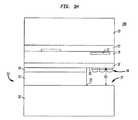
ここで、背面照明イメージセンサを作製する方法が、図1A〜図1Oの個々の作製段階
を示す断面図を参照しながら説明される。図1Aに示されるように、パッケージングプロ
セスが実行される前の作製の準備段階では、半導体材料ウェハ10が設けられ、ウェハ1
0の表面11上にプロセス停止層12が配置される。ウェハ10は本質的にシリコンから
なることがあり、代替的には、例えば、ゲルマニウム(Ge)、炭素(C)、シリコンと
そのような材料との合金若しくは組み合わせ、又はそれぞれ周期表のIII族元素とV族
元素との化合物である1つ以上のIII−V化合物半導体材料等の他の半導体材料を含み
うる。一実施形態では、層12は、約1μm〜約5μmの厚みを有することができ、本質
的に二酸化シリコンからなることがある。Here, a method of manufacturing a back-illuminated image sensor will be described with reference to cross-sectional views showing individual manufacturing steps of FIGS. As shown in FIG. 1A, in a preparation stage of fabrication before the packaging process is performed, a
A
図1Bを参照すると、ウェハ10と同一又は類似の材料から形成される半導体デバイス
ウェハ14が、層12の露出面15においてウェハ10と接合される。図1Cを参照する
と、ウェハ10及び14が接合された後に、ウェハ14を研削するか、又はスマートカッ
トすること等によって、ウェハ14の厚みが薄くされる。Referring to FIG. 1B, a
ウェハ14は、本質的にシリコンからなることがあるアクティブ半導体層又はアクティ
ブ領域を含む。図1A〜図1Oには示されていないが、ウェハ14は、それぞれイメージ
センシング領域を構成する複数の隣接するダイを含む。図1Dを参照すると、各センシン
グ領域がアクティブ領域内に形成されるイメージセンサ17を含む。イメージセンサは複
数の光検出器素子を含み、それらの素子は通常はアレイとして配列され、ウェハ14の前
面又は背面に対して垂直な方向の光を介してその上に投じられる画像を取り込むための1
つ以上の画素(ピクセル)を形成する。一例では、イメージセンサは、電荷結合素子(「
CCD」)アレイでありうる。別の例では、イメージセンサは、相補型金属酸化膜半導体
(「CMOS」)デバイスアレイでありうる。ウェハ14のセンシング領域又はダイはそ
れぞれ、後の作製段階において互いに切り離される。本発明の特徴を強調するために、図
1A〜図1Oには、ウェハ14を含む超小型電子アセンブリ100の単一のイメージセン
シング領域の一部が示される。アセンブリ100の作製処理がアセンブリ100の単一の
イメージセンシング領域に関して以下に説明されるが、同じ作製処理が、アセンブリ10
0の他のイメージセンシング領域において行われることを理解されたい。
One or more picture elements (pixels) are formed. In one example, the image sensor is a charge coupled device (“
CCD ") array. In another example, the image sensor can be a complementary metal oxide semiconductor (“CMOS”) device array. Each sensing region or die of the
It should be understood that this is done in zero other image sensing areas.
一実施形態では、ウェハ14は最終的な厚みまで薄くすることができ、その厚みは、ウ
ェハ14の表面に沿った横方向における、センサ17内に形成されるピクセルの横寸法と
同じである。他の実施形態では、ウェハ14は約3μm〜約5μmの最終的な厚みを有す
る。In one embodiment, the
更に図1Dを参照すると、ウェハ14の厚みが薄くされた後に、ボンドパッド16がウ
ェハ14の前面19上に形成される。オプションでは、ボンドパッド16は、前面19に
配置される誘電体層(図示せず)の上に重なることができる。Still referring to FIG. 1D, after the thickness of the
本明細書において用いられるときに、「上部」、「底部」、「上方の」又は「上方に」
及び「下方の」又は「下方に」等の用語は超小型電子素子、例えば、半導体ウェハ若しく
はチップ、又はそのようなウェハ若しくはチップを組み込むアセンブリ若しくはユニット
の座標系を指している。これらの用語は、通常の重力座標系を指していない。参照しやす
いように、本明細書では、デバイスウェハ14の「上面」又は「前面」19を基準にして
方向が示される。通常、「上方」又は「〜から上昇」と称される方向は、前面19に直交
しかつ前面19から離れる方向を指すものとする。「下方」と称される方向は、前面19
に直交しかつ上方向と反対の方向を指すものとする。「垂直」方向は、チップ前面に直交
する方向を指すものとする。基準点「の上」という用語は、基準点の上方の点を指すもの
とし、基準点「の下」という用語は、基準点の下方の点を指すものとする。任意の個々の
素子の「上部」は、上方において最も離れて延在する、その素子の単数又は複数の点を指
すものとし、任意の素子の「底部」という用語は、下方において最も離れて延在する、そ
の素子の単数又は複数の点を指すものとする。As used herein, “top”, “bottom”, “upper” or “upward”
And terms such as “down” or “down” refer to the coordinate system of a microelectronic element, such as a semiconductor wafer or chip, or an assembly or unit incorporating such a wafer or chip. These terms do not refer to the normal gravitational coordinate system. For ease of reference, the direction is indicated herein with respect to the “top” or “front” 19 of the
It is assumed to point in a direction orthogonal to the upper direction and opposite to the upward direction. The “vertical” direction refers to a direction orthogonal to the front surface of the chip. The term “above” the reference point shall refer to a point above the reference point, and the term “below” the reference point shall refer to a point below the reference point. The “top” of any individual element shall refer to the point or points of that element that extend the farthest upward, and the term “bottom” of any element extends the farthest downward. It shall refer to one or more points of the device.
本明細書において用いられるとき、導電性構造体が誘電体構造体の面「において露出し
ている」という記述は、導電性構造体が、誘電体構造体の面に対して垂直である方向にお
いて、誘電体構造体の外側から誘電体構造体の面に向かって移動している理論的な点に接
触することができることを示す。したがって、誘電体構造体の面において露出している端
子又は他の導電性構造体は、このような面から突出することができるか、このような面と
同一平面とすることができるか、又はこのような面に対して凹状であり、誘電体の孔又は
窪みを通して露出することができる。As used herein, the description that a conductive structure is “exposed in the plane of the dielectric structure” means that the conductive structure is perpendicular to the plane of the dielectric structure. It shows that a theoretical point moving from the outside of the dielectric structure toward the surface of the dielectric structure can be contacted. Thus, a terminal or other conductive structure exposed at the surface of the dielectric structure can protrude from such a surface, can be coplanar with such a surface, or It is concave to such a surface and can be exposed through a hole or depression in the dielectric.
図1Eを参照すると、キャリアウェハ又はパッケージング層20が、接着剤22を用い
て、前面19においてウェハ14に接合される。接着剤22は、任意の適切な材料とする
ことができ、エポキシでありうる。接着剤22は、後続の熱処理中に受けることになる最
大の加熱に耐える特性、及び最大の加熱に耐えるだけの十分に高いガラス転移温度Tgを
有するべきである。接着剤22は、前面19を覆うことができる。好ましくは、接着剤は
、米国特許第5,980,663号明細書及び第6,646,289号明細書において記
述されるようなスピンボンディングによって均質に塗布され、それらの特許の開示は引用
することにより本明細書の一部をなすものとする。代替的には、任意の他の適切な技法を
利用することができる。別の実施形態では、酸化物/窒化物層を用いて、パッケージング
層20をデバイスウェハ14に接合することができる。Referring to FIG. 1E, a carrier wafer or
層20は、デバイスウェハ14の熱膨張係数に一致する熱膨張係数を有するように、シ
リコン、ガラス又はセラミック等の材料から形成することができる。一例では、パッケー
ジング層20は、ウェハ14に最初に接合されるときに、約500μm〜約1000μm
の厚みを有することができる。
The thickness can be as follows.
図1Fを参照すると、アセンブリ100のウェハ10が、エッチング及び/又は研削等
によって、完全に除去される。一実施形態では、ウェハ10は、最初に機械的に研削又は
粗研磨して、ウェハ10の数マイクロメートルの厚みを除いて全て除去し、その後、エッ
チングを実行して、ウェハ10の残りの数マイクロメートルを除去する。アセンブリ10
0の層12はエッチストップとしての役割を果たすことができ、言い換えると、ウェハ1
0が除去されるときに、イメージセンシング領域を含むデバイスウェハ14の部分がエッ
チング(除去)されるのを防ぐことがきる。Referring to FIG. 1F, the
The zero
When 0 is removed, the portion of the
特定の実施形態では、層10を数マイクロメートルの厚みまで機械的に研削した後に、
化学及び/又は機械研磨を実行して、層10の残りの厚みを除去することができる。In certain embodiments, after mechanically grinding
Chemical and / or mechanical polishing can be performed to remove the remaining thickness of
代替の実施形態では、バルク層10が完全に除去された後に、層12を完全に除去する
ことができ、その後、制御された厚みを有することができる透明誘電体等の、別の材料層
をデバイスウェハ14の露出した背面23上に設けることができる。一例では、代わりと
なる透明層は、反射防止層を含みうる。In an alternative embodiment, after the
図1Gを参照すると、層12が除去されない場合に、誘電体層12の露出した背面26
上に反射防止コーティング(具体的には示されない)を形成することができる。反射防止
コーティングは、ウェハ14の表面23から反射される光の量を低減し、コントラスト比
を改善するのを助けることができる。反射防止コーティングは、二酸化シリコン、フッ化
マグネシウム及び/又は酸化インジウムスズを含みうる。Referring to FIG. 1G, the exposed back
An antireflective coating (not specifically shown) can be formed thereon. The antireflective coating can help reduce the amount of light reflected from the
その後、カラーフィルタ28を含むカラーフィルタアレイを表面26の上に重なるよう
に形成又は積層することができる。カラーフィルタ28を用いて、カラーフィルタに達す
る光の波長を異なる色範囲に対応する異なる波長範囲に分離し、波長によって分離された
光をカラーフィルタからデバイスウェハ14の背面23に向かって伝搬させることができ
る。ウェハ14内のイメージセンサ17の単数又は複数のピクセルとそれぞれ位置合わせ
された、種々の異なるカラーフィルタを使用することにより、各カラーフィルタ及びピク
セルを用いて、特定の色範囲に対応する限られた所定の範囲の波長のみを検知することが
できる。そのようにして、均質な光検出器素子のアレイを、異なる色を透過するように適
合したカラーフィルタの適切な組み合わせとともに用いて、数多くの異なる色の組み合わ
せを検出できるようになる。Thereafter, a color filter array including the
そして、カラーフィルタ28のアレイの露出面の上に重なる複数組のマイクロレンズ3
0を形成することができる。マイクロレンズ30は、アレイとして配列される屈折材料か
らなる小さなバンプを含み、それらのバンプはデバイスウェハ14のイメージセンサの1
つ以上のピクセル上に光を合焦するのを助ける。マイクロレンズ30の露出面30Aに達
する光は、主に1つ以上の対応するピクセルに向けられる。Then, a plurality of sets of microlenses 3 overlapping the exposed surface of the array of color filters 28.
0 can be formed. The
Help focus the light on more than one pixel. Light reaching the exposed
図1Hに更に示されるように、パッケージングアセンブリ31の側壁又はスタンドオフ
を構成するパッケージング層32を、接着剤34を用いて、誘電体層12の背面26に取
り付けることができる。側壁32は、レンズ30を含むアセンブリ100の領域の上に垂
直方向に重ならないように取り付けることができる。側壁32は誘電体材料から形成する
ことができる。さらに、側壁32の背面35に蓋又はカバー用ウェハ36が接合される。
側壁32を層12に取り付けることができ、そして、蓋ウェハ36が側壁32に取り付け
られる。代替的には、側壁32及び蓋ウェハ36は最初に互いに取り付けられ、そして、
側壁32が蓋ウェハ36とともに層12に取り付けられる。側壁32及び蓋ウェハ36は
合わせて、デバイス14のセンシング領域に関連付けられるフィルタ及びマイクロレンズ
を封入する空洞37を画定する。As further shown in FIG. 1H, the
A
蓋ウェハ36は、イメージセンサ17内に組み込まれる光検出器素子の対象波長に対し
て少なくとも部分的に透過性であり、1つ以上の種々のタイプのガラスから形成すること
ができ、無機材料若しくは有機材料、又はその組み合わせを含みうる。空洞37は、層1
2の背面26と蓋ウェハ36の向かい合う面との間に延在する高さ又は垂直寸法D1を有
することができ、D1は約35μm〜約40μmである。イメージセンサの背面に接合さ
れるパッケージングアセンブリの詳細な説明に関しては、例えば、引用することにより本
明細書の一部をなすものとする、米国特許出願第12/583,830号を参照されたい
。The
2 may have a height or vertical dimension D1 extending between the
図1Iに示されるように、蓋ウェハ36をデバイスウェハ14に取り付けた後に、パッ
ケージング層20を約30μm以上の厚みまで研削することができる。層20は、アセン
ブリ100のための機械的な支持体としての役割を果たすだけの十分な剛性を有するよう
な最終的な厚みを有する。As shown in FIG. 1I, after the
図1Jに示されるように、パッケージング層20の前面42内に凹部40を形成するこ
とができる。凹部40は、層20の外面42Aから接着剤22の内面43まで内向きに延
在する。一実施形態では、フォトリソグラフィを用いて、層20の前面42の上に重なる
マスクパターン(図示せず)を形成することができ、その後、ウエットエッチング又はド
ライエッチングを用いて、層20を前面42からエッチングすることができる。接着剤2
2は、凹部40が形成されるときにデバイスウェハ14がエッチングされるのを回避する
エッチストップ層として機能する。代替的な実施形態では、凹部40は、層20のレーザ
アブレーションによって形成することができる。別の実施形態では、引用することにより
本明細書の一部をなすものとする、2010年7月23日に出願の同じ譲受人に譲渡され
た同時係属の米国特許出願第12/842,612号において開示されるような、方向性
の粒子流を用いて層20をサンドブラストして、凹部40を形成することができる。A
2 functions as an etch stop layer that prevents the
一実施形態では、凹部40は、ボンドパッド16の上に重なる場所にのみ形成される個
別のビアホール又は切欠きとすることができる。別の代替の実施形態では、凹部40は、
アセンブリ100の接着層22の表面43にわたって連続して延在する溝の形をとること
ができる。例えば、引用することにより本明細書の一部をなすものとする、2008年2
月26日に出願の米国特許出願第12/072,508号、及び2009年8月26日に
出願の米国特許出願第12/583,830号を参照されたい。In one embodiment, the
It can take the form of a groove that extends continuously across the
See U.S. Patent Application No. 12 / 072,508 filed on May 26, and U.S. Patent Application No. 12 / 583,830 filed August 26, 2009.
図1Kに示されるように、パッケージング層20の前面42、凹部40内の層20の側
壁表面44及び凹部40の底部における接着剤22の内面43の露出部分を含む、アセン
ブリ100の露出した前面の全ての上に、ポリマ層又はパッシベーション層50が形成さ
れる。図1Kを参照すると、層50は、接着剤22の表面43上にあり、ボンドパッド1
6の上に重なる下側部分52と、層20の前面42上にある上側部分54と、層20の側
壁表面44上にある側壁部分56とを含む。層50は、例えば、スプレー若しくはスピン
コーティング、電解析出若しくは電気泳動析出、酸化物化学気相成長又はプラズマ化学気
相成長によって形成することができる。層50は、コンプライアンスを与えるほど十分な
厚みを有するように形成することができるか、代替的には、酸化物層等の非コンプライア
ント層とすることができる。引用することにより本明細書の一部をなすものとする、20
09年8月26日に出願された米国特許出願第12/583,830号を参照されたい。As shown in FIG. 1K, the exposed front surface of the
6 includes a
See US patent application Ser. No. 12 / 583,830, filed Aug. 26, 2009.
図1Lに示されるように、層50の下側部分52を貫通して凹部60を形成することが
できる。凹部60は、層50と、その下側の接着剤22とを貫通してボンドパッド16ま
で、そしてボンドパッド16の中まで垂直に延在する。凹部60は、ボンドパッド16の
中に部分的にのみ延在することができる。一実施形態では、凹部60が形成されるときに
、ボンドパッド16の前面において、ボンドパッド16の1マイクロメートル未満の厚み
が除去される。凹部60は、制御されたレーザエッチング又はアブレーションによって形
成することができ、その場合、そのパルス幅、強度、数及び波長を適切に制御して、層5
0の部分52の全て又は或る部分と、層50のアブレートされた部分52の下層を成し、
かつ垂直に位置合わせされた接着剤22の部分と、接着剤22のアブレートされた部分の
下層を成しかつ垂直に位置合わせされたボンドパッド16の所定の厚みと、を垂直にアブ
レートする。例えば、引用することにより本明細書の一部をなすものとする、2008年
7月31日に出願の米国特許出願第12/221,204号を参照されたい。A
Forming all or some of the zero
The vertically aligned portion of the adhesive 22 and the predetermined thickness of the vertically aligned
別の実施形態では、ボンドパッド16へのアブレーション深度は、ボンドパッドの厚み
の10%以下である。更なる実施形態では、ボンドパッド16へのアブレーション深度は
、ボンドパッドの厚みの50%以上まで延在することができる。図1Mに関連して後に説
明されるように、後に被着される相互接続金属のために、信頼性があり、かつ低抵抗のオ
ーミックコンタクトを形成できるように、ボンドパッドの金属面のアブレーションによっ
て、汚れのない金属が露出されるようにすることが有利である。In another embodiment, the ablation depth to the
一実施形態では、凹部60は、デバイスウェハ14のアクティブ構成要素がボンドパッ
ド16の下にないときに、ボンドパッド16を完全に貫通して延在することができる。In one embodiment, the
図1L及び図1Mを参照すると、パッシベーション層50の上側部分54の露出面上に
シード金属層70が選択的に形成され、凹部40及び凹部60内の層50の露出面、凹部
60内の接着層22の露出面58及びボンドパッド16の露出面上にも形成される。層7
0は、スパッタリング又はブランケットメタライゼーションと、その後のフォトリソグラ
フィを用いる表面パターニングとによって形成することができる。引用することにより本
明細書の一部をなすものとする、2006年11月22日に出願された米国特許出願第1
1/603,935号を参照されたい。代替的には、シード金属層70は無電解めっきに
よって形成することができる。Referring to FIGS. 1L and 1M, a
O can be formed by sputtering or blanket metallization followed by surface patterning using photolithography. U.S. Patent Application No. 1 filed on Nov. 22, 2006, which is hereby incorporated by reference.
See 1 / 603,935. Alternatively, the
図1Nに示されるように、マスク用誘電体層80が、層50の上側部分54の露出面上
、及び層70の露出した前面72上にパターニングされて形成され、ハンダバンプ位置9
0を画定する。さらに、凹部40及び60内の層70の露出面上に層80が形成される。
一実施形態では、層80の材料は、凹部40及び凹部60の全体を満たすことができる。As shown in FIG. 1N, a masking
0 is defined. Further, a
In one embodiment, the material of
図1Oに示されるように、ハンダマスク80が存在していない層70上の場所90にお
いて、ハンダバンプ96を形成することができる。引用することにより本明細書の一部を
なすものとする、米国特許出願第12/583,830号を参照されたい。As shown in FIG. 1O, solder bumps 96 can be formed at
一実施形態では、図1A〜図1Oの方法に従って製造されるパッケージされたイメージ
センサユニットを、例えば、米国特許出願第12/583,830号において記述される
ように、それぞれがアクティブ領域を含む超小型電子ユニットを構成する個々のパッケー
ジされたチップアセンブリ100に単体化することができる。In one embodiment, packaged image sensor units manufactured according to the method of FIGS. 1A-1O may be manufactured as described in, for example, US patent application Ser. No. 12 / 583,830. It can be singulated into individual packaged
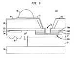
図2を参照すると、本発明の別の実施形態では、超小型電子アセンブリ200のデバイ
スウェハ14上に、アセンブリ100のボンドパッド16に関連する厚みを増したボンド
パッド216を設けることができる。アセンブリ200は、ボンドパッド216を除いて
、アセンブリ100の構成に類似の構成を有し、同じ参照番号が同一又は類似の要素を示
す。ボンドパッド216は、デバイスウェハ14の前面19と接触する金属層216Bと
、金属層216B上に配置される金属層216Aとを含む。層216A、216Bによっ
て、前面19から離れて延在するボンドパッド216の厚みが、後に塗布される接着剤2
2と概ね同じ厚みになるようにする。凹部60は、ボンドパッド216の金属層216A
内で終端するように形成することができる。凹部60は、アセンブリ100のボンドパッ
ド16の厚みと概ね同じ厚みを有する金属層216Bの中に延在しないことが望ましい。Referring to FIG. 2, in another embodiment of the present invention, an increased
The thickness is approximately the same as 2. The
Can be formed to terminate within. The
ボンドパッド216は、ボンドパッド16よりも厚い厚みを有し、凹部60、それゆえ
、パッケージングプロセス中に形成される金属層70がボンドパッド216内で終端し、
デバイスウェハ14と接触しないようにする。結果として、センサ17のような、デバイ
スウェハ14のアクティブ領域は、凹部60内の金属層70から電気的に分離される。一
実施形態では、金属層216Bがデバイスウェハ14の前面19上に形成された後に、金
属層216B上に金属層216Aを形成することによってボンドパッド216が設けられ
ることを除いて、アセンブリ200の作製は、アセンブリ100の場合に上述されたのと
概ね同じように実行することができる。The
Avoid contact with the
ボンドパッド216は、0.5μmよりもはるかに厚い厚みを有することができ、レー
ザアブレーションに耐える金属又は他の材料を含みうる。例えば、層216Aのために用
いられる金属は、層216Bを形成するアルミニウムよりも、レーザアブレーションに耐
えることができる。レーザアブレーションに耐えること、コストが低いこと、及び標準的
な無電解めっきプロセスによって容易に堆積されることに基づいて、層216Aを形成す
るためにニッケル、銅、金、銀等の材料が望ましい。The
一実施形態では、ボンドパッド216は、アルミニウムから形成された層216B上に
配置される、ニッケル、銅、金又は銀から形成された層216Aを含みうる。一実施形態
では、層216Aの厚みは、ボンドパッド216の厚みの50%よりも厚くすることがで
きる。層216Aの厚みは3μm〜5μmとすることができ、0.5μm〜30μmとす
ることができる。In one embodiment, the
本発明によれば、同じ面上にアクティブ領域及びボンドパッドを有する前面照明センサ
アセンブリにおいて、厚みを増したボンドパッドを形成することもでき、その場合、更な
る作製ステップ中にアセンブリが反転されることを理解されたい。In accordance with the present invention, a thickened bond pad can also be formed in a front illumination sensor assembly having an active area and bond pad on the same surface, in which case the assembly is inverted during further fabrication steps. Please understand that.
図3を参照すると、本発明の更なる実施形態では、超小型電子アセンブリ300内に含
まれるデバイスウェハ14内に、複数のレベル又は層を有するボンドパッド316を設け
ることができる。アセンブリ300は、ボンドパッド316を除いて、アセンブリ100
の構成に類似の構成を有し、同じ参照番号が同一又は類似の要素を示す。ボンドパッド3
16は、イメージセンサ17のピクセルを形成するために実行される一連のステップの一
部として作製することができる。ボンドパッド316は幾つかの金属層316Aを含み、
各金属層316Aは、上記のアセンブリ100のボンドパッド16等の単層ボンドパッド
と同一又は類似の構成を有することができる。層316Aは、導電性ビア316B又は他
の導電性垂直構造体によって互いに接続される。一実施形態では、金属層316A及びビ
ア316はウェハ14内の半導体材料から分離することができる。ボンドパッド316は
、図3に示されるように、ウェハ14内に部分的に、又は完全に凹所を作るように作製す
ることができるか、代替的には、ウェハ14の表面19上に形成することができる。凹部
60は、ウェハ14の背面23に最も近いボンドパッド316の金属層316Aの背面に
届かない深さまでボンドパッド316内に延在するように形成されることが望ましい。結
果として、センサ17のような、ウェハデバイス14のアクティブ領域は、凹部60内の
金属層70から電気的に分離される。アセンブリ300の作製は、デバイスウェハ14内
にボンドパッド316が形成されることを除いて、アセンブリ100の場合に上述された
のと概ね同じように実行することができる。Referring to FIG. 3, in a further embodiment of the present invention, a
The same reference numerals indicate the same or similar elements. Bond pad 3
16 can be made as part of a series of steps performed to form the pixels of the
Each
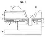
図4を参照すると、本発明の別の実施形態では、超小型電子アセンブリ350において
、電気的分離領域360が、ボンドパッド16の背面361、及びデバイスウェハ14の
背面19から離れるように延在する。アセンブリ350は、アセンブリ100の構成に類
似の構成を有し、同じ参照番号が同一又は類似の要素を示す。領域360はボンドパッド
16の背面361の一部によって部分的に画定され、その部分は、そこを貫通して凹部6
0が形成されるボンドパッド16の部分を完全に取り囲む。領域360は、二酸化シリコ
ンのような誘電体材料で満たすことができ、側壁32の一部とすることができる。代替的
には、領域360は、側壁32をウェハ14に取り付けるために用いられるのと同じ接着
材料で満たすことができる。Referring to FIG. 4, in another embodiment of the present invention, in
It completely surrounds the portion of the
領域360内の材料は、凹部60の側壁に沿って延在する金属層70をウェハ14のセ
ンサ17のようなアクティブ領域から電気的に分離する。上述したように、金属層70は
、凹部60内のボンドパッド16の径方向に対称なコンタクト領域においてボンドパッド
16と接触していることが望ましい。領域360によって、金属層70はウェハ14から
電気的に分離されるようになる。図4に示されるように、凹部60は、ボンドパッド16
の全体を貫通して延在するように形成することができ、領域360、接着層34及び/又
は側壁32内の材料のような、ボンドパッド16の下層を成す1つ以上の材料層を貫通し
て延在する場合もある。The material in
Through one or more material layers underlying the
側壁32を取り付ける前に層12を除去することができ、そして、フォトリソグラフィ
及びエッチングを使用すること等により、ウェハ14の一部を除去することによってボン
ドパッド16の下層を成す領域360が形成されることを除いて、アセンブリ350の作
製は、アセンブリ100の場合に上述したのと概ね同じように実行することができる。望
ましくは、領域360は、デバイスウェハ14の厚みが薄くされた後に形成される。The
図5を参照すると、本発明の別の実施形態では、アセンブリ100に類似の構成を有す
る超小型電子アセンブリ400が、デバイスウェハ14内に分離領域又はトレンチ410
を含みうる。アセンブリ400は、アセンブリ100の構成に類似の構成を有し、同じ参
照番号が同一又は類似の要素を示す。トレンチ410は、ボンドパッド16を完全に取り
囲み、少なくとも部分的に、そして一実施形態では完全にウェハ14を貫通して延在する
。Referring to FIG. 5, in another embodiment of the present invention, a
Can be included.
トレンチ410は、誘電体材料で満たすことができる。代替的には、トレンチ410は
、トレンチ410に隣接し、かつトレンチによって取り囲まれるウェハ14の半導体領域
のドーピングとは異なるドーピングを有するウェハ14のドープ半導体領域である。トレ
ンチ410が、トレンチ410の一方にある、トレンチ410によって取り囲まれるウェ
ハ14の隣接する領域と、トレンチ410を挟んで凹部60の反対側にあるウェハ14の
領域と、の間に電気的分離を与えるように、トレンチ410と隣接する領域との間のドー
ピングの差を適応させる。ドープされたトレンチ410は、例えば、PINダイオードの
真性領域(I)によって与えられるのと同じような電気的分離を与えることができる。The
トレンチ410は、ボンドパッド16の真下に延在し、凹部60内の金属層70と接触
することができるウェハ14の部分を、センサ17のようなイメージング素子を含む、ウ
ェハ14の残りの部分から電気的に分離する。実際には、トレンチ410はウェハ14内
の高抵抗率の素子であり、ウェハ14内に電気的な島状部を作り出す。トレンチ410は
、ボンドパッド16を取り囲むことによって、ボンドパッド16を貫通してボンドパッド
16下のウェハ14の中に延在するように、レーザエッチングを用いて凹部60を形成で
きるようにする。トレンチ410は、センサ17のようなウェハ14のアクティブ部分が
、凹部60内に形成される金属層70の部分と短絡するのを避ける。The
トレンチ410が好ましくは、イメージセンサ17のピクセルを形成する一連のステッ
プの一部として、かつ側壁32及び蓋ウェハ36を含むパッケージングアセンブリ31が
ウェハ14に取り付けられる前に、半導体ウェハ14の作製中に形成されることを除いて
、アセンブリ400の作製は、アセンブリ100の場合に上述したのと概ね同じように実
行することができる。The
本発明は特定の実施形態を参照しながら本明細書において説明されてきたが、これらの
実施形態は本発明の原理及び応用形態を例示するにすぎないことを理解されたい。そのた
め、添付の特許請求の範囲によって規定されるような本発明の趣旨及び範囲から逸脱する
ことなく、例示的な実施形態に数多くの変更を加えることができること、及び他の構成を
考案することができることを理解されたい。Although the invention has been described herein with reference to particular embodiments, it is to be understood that these embodiments are merely illustrative of the principles and applications of the present invention. Thus, numerous modifications can be made to the exemplary embodiments and other arrangements can be devised without departing from the spirit and scope of the invention as defined by the appended claims. Please understand that you can.
Claims (45)
Translated fromJapanese前面と該前面から離れた背面とを有する半導体素子と、
前記半導体素子の前記前面に取り付けられるパッケージング層と、
ここで、前記半導体素子は、前記前面に隣接して配置され、前記背面の一部分を通して
光を受光するために該背面の該部分と位置合わせされる光検出器と、前記前面にあり、該
光検出器に接続される導電性コンタクトとを含み、前記光検出器は、アレイとして配列さ
れる複数の光検出器素子を含み、前記導電性コンタクトは、第1の厚みを有する薄い領域
と、該第1の厚みよりも厚い第2の厚みを有する厚い領域とを含んでおり、
前記パッケージング層を貫通して前記導電性コンタクトの前記薄い領域まで延在する導
電性相互接続であって、該導電性相互接続の少なくとも一部は該超小型電子ユニットの表
面において露出する、導電性相互接続と
を備えてなる、超小型電子ユニット。A microelectronic unit,
A semiconductor element having a front surface and a back surface away from the front surface;
A packaging layer attached to the front surface of the semiconductor element;
Wherein the semiconductor element is disposed adjacent to the front surface and is aligned with the portion of the back surface for receiving light through a portion of the back surface; A conductive contact connected to a detector, wherein the photodetector includes a plurality of photodetector elements arranged in an array, the conductive contact comprising a thin region having a first thickness; A thick region having a second thickness greater than the first thickness,
A conductive interconnect extending through the packaging layer to the thin region of the conductive contact, wherein at least a portion of the conductive interconnect is exposed at a surface of the microelectronic unit. An ultra-compact electronic unit comprising
子ユニット。The microelectronic unit of claim 1, wherein the first thickness is 90 percent of the second thickness.
子ユニット。The microelectronic unit of claim 1, wherein the first thickness is 50 percent of the second thickness.
検出器と位置合わせされる空洞を画定するパッケージングアセンブリを更に備える、請求
項1に記載の超小型電子ユニット。The microelectronic unit of claim 1, further comprising a packaging assembly attached to the back surface of the semiconductor element and defining a cavity aligned with the photodetector in a direction perpendicular to the back surface.
グアセンブリが取り付けられる第1の誘電体層を更に備える、請求項4に記載の超小型電
子ユニット。5. The microelectronic unit of claim 4, further comprising a first dielectric layer disposed on the back surface of the semiconductor element and to which the packaging assembly is attached through a second dielectric layer.
2の誘電体層は接着材料を含む、請求項5に記載の超小型電子ユニット。The microelectronic unit according to claim 5, wherein the first dielectric layer has a thickness of 1 micrometer to 5 micrometers, and the second dielectric layer includes an adhesive material.
する、請求項1に記載の超小型電子ユニット。The microelectronic unit of claim 1, wherein the packaging layer has a thickness of 30 micrometers to 1000 micrometers.
記半導体素子の厚みに等しい、前記前面に沿った横方向における横寸法を有する、請求項
1に記載の超小型電子ユニット。The photodetector of claim 1, comprising a plurality of photoelements defining one or more pixels, each pixel having a lateral dimension along the front surface equal to the thickness of the semiconductor element. Ultra-small electronic unit.
請求項1に記載の超小型電子ユニット。A layer comprising an adhesive material for attaching the semiconductor element to the packaging layer;
The microelectronic unit according to claim 1.
を含み、前記半導体素子は、該第3の厚みよりも厚い第4の厚みを有し、
前記導電性相互接続は、前記第3の厚み未満の深さまで、前記導電性コンタクトの中に
延在し、前記導電性相互接続は、前記導電性コンタクトの前記複数の層のうちの金属層に
接続する、請求項1に記載の超小型電子ユニット。The conductive contact is disposed in the semiconductor element and includes a plurality of layers having a third thickness, and the semiconductor element has a fourth thickness greater than the third thickness;
The conductive interconnect extends into the conductive contact to a depth less than the third thickness, and the conductive interconnect extends to a metal layer of the plurality of layers of the conductive contact. The microelectronic unit according to claim 1, which is connected.
の超小型電子ユニット。The microelectronic unit of claim 10, wherein the plurality of layers of the conductive contact includes a layer comprising a dielectric material.
を含む、請求項10に記載の超小型電子ユニット。The microelectronic unit of claim 10, wherein the conductive contact includes a conductive via that interconnects adjacent layers of the plurality of layers.
項10に記載の超小型電子ユニット。The microelectronic unit of claim 10, wherein the plurality of layers of the conductive contact includes alternating layers of dielectric material layers and metal layers.
ユニット。The microelectronic unit of claim 10, wherein the third thickness is a maximum of 10 micrometers.
ジング層に向かって延在しており、
前記導電性相互接続は、前記第2の厚み未満の深さまで、前記導電性コンタクトの中に
延在している、請求項1に記載の超小型電子ユニット。The thin region and the thick region of the conductive contact extend from the front surface toward the packaging layer;
The microelectronic unit of claim 1, wherein the conductive interconnect extends into the conductive contact to a depth less than the second thickness.
記パッケージング層との間に配置される少なくとも1つの第2の金属層とを含む、請求項
15に記載の超小型電子ユニット。The conductive contact includes a first metal layer adjacent to the front surface and at least one second metal layer disposed between the first metal layer and the packaging layer. 15. The microelectronic unit according to 15.
のうちの少なくとも1つを含む、請求項16に記載の超小型電子ユニット。17. The microelectronic unit according to claim 16, wherein the first metal layer includes aluminum, and the second metal layer includes at least one of nickel, copper, silver, or gold.
ユニット。The microelectronic unit according to claim 16, wherein the second metal layer is formed by electrodeless plating.
超小型電子ユニット。The microelectronic unit according to claim 16, wherein the second metal layer has a thickness greater than that of the first metal layer.
請求項16に記載の超小型電子ユニット。The second metal layer has a thickness of 0.5 to 30 micrometers;
The microelectronic unit according to claim 16.
うな深さまで前記導電性コンタクトの中に延在する、請求項16に記載の超小型電子ユニ
ット。17. The microelectronic unit of claim 16, wherein the conductive interconnect extends into the conductive contact to a depth that terminates between the first metal layer and the packaging layer.
検出器と位置合わせされる空洞を画定するパッケージングアセンブリを更に備える、請求
項15に記載の超小型電子ユニット。16. The microelectronic unit of claim 15, further comprising a packaging assembly attached to the back surface of the semiconductor element and defining a cavity aligned with the photodetector in a direction perpendicular to the back surface.
半導体素子の前面に取り付けられたパッケージング層を貫通して延在し、導電性コンタ
クトの薄い領域において終端する凹部を形成するステップであって、該導電性コンタクト
は前記半導体素子の前記前面に配置され、該半導体素子は該前面から離れた背面を有し、
該前面に隣接して配置され、前記導電性コンタクトに接続され、前記背面の一部分を通し
て光を受光するために該背面の該部分と位置合わせされる光検出器を含み、該光検出器は
アレイとして配列される複数の光検出器素子を含み、前記導電性コンタクトは、前記薄い
領域において第1の厚みを有し、該第1の厚みよりも厚い第2の厚みを有する厚い領域を
含むステップと、
前記凹部を貫通して延在し、前記薄い領域において前記導電性コンタクトに接続する導
電性相互接続を形成するステップであって、該導電性相互接続の少なくとも一部は前記超
小型電子ユニットの表面において露出するステップと
を含んでなる、超小型電子ユニットを形成する方法。A method of forming a microelectronic unit,
Forming a recess extending through a packaging layer attached to the front surface of the semiconductor element and terminating in a thin region of the conductive contact, the conductive contact being disposed on the front surface of the semiconductor element The semiconductor element has a back surface away from the front surface;
A photodetector disposed adjacent to the front surface, connected to the conductive contact and aligned with the portion of the back surface for receiving light through the portion of the back surface, the light detector comprising an array A plurality of photodetector elements arranged as: the conductive contact including a thick region having a first thickness in the thin region and a second thickness greater than the first thickness. When,
Forming a conductive interconnect extending through the recess and connecting to the conductive contact in the thin region, wherein at least a portion of the conductive interconnect is a surface of the microelectronic unit Exposing a microelectronic unit comprising the steps of:
する複数の超小型電子素子を含み、凹部を形成する前記ステップは、前記複数の超小型電
子素子のそれぞれにおいて凹部を形成し、導電性相互接続を形成する前記ステップは、前
記複数の超小型電子素子のそれぞれにおいて導電性相互接続を形成し、
その上に前記パッケージング層を有する前記半導体素子を複数の個々の超小型電子ユニ
ットに切り離すステップを更に含む、請求項23に記載の方法。The semiconductor element includes a plurality of microelectronic elements attached together at a periphery thereof, each having an individual photodetector, and the step of forming a recess is performed in each of the plurality of microelectronic elements. The step of forming a recess and forming a conductive interconnect forms a conductive interconnect in each of the plurality of microelectronic elements;
24. The method of claim 23, further comprising separating the semiconductor device having the packaging layer thereon into a plurality of individual microelectronic units.
、前記導電性コンタクトをアブレートし、前記薄い領域において前記第1の厚みを得るこ
とを含む、請求項23に記載の方法。24. The method of claim 23, wherein the forming the recess comprises ablating the conductive contact using light energy supplied by a laser to obtain the first thickness in the thin region. .
の前記形成中に制御される、請求項25に記載の方法。26. The method of claim 25, wherein the intensity, wavelength and duration of the light energy supplied by the laser is controlled during the formation of the recess.
あって、前記背面に対して垂直な方向において前記光検出器と位置合わせされる空洞を画
定するステップを更に含む、請求項23に記載の方法。24. The mounting of a packaging assembly on the back surface of the semiconductor device, further comprising defining a cavity that is aligned with the photodetector in a direction perpendicular to the back surface. Method.
けるステップを更に含む、請求項23に記載の方法。24. The method of claim 23, further comprising attaching a first dielectric layer on the back surface of the semiconductor element prior to the formation of the recess.
られ、そして、パッケージングアセンブリの一部であるガラス層が前記第1の誘電体層に
取り付けられ、それによって前記パッケージングアセンブリが前記背面に対して垂直な方
向において前記光検出器と位置合わせされる空洞を画定する、請求項30に記載の方法。Prior to the formation of the recess, the first dielectric layer is attached to the back surface of the semiconductor device, and a glass layer that is part of a packaging assembly is attached to the first dielectric layer; 32. The method of claim 30, wherein the packaging assembly defines a cavity that is aligned with the photodetector in a direction perpendicular to the back surface.
るガラス層に取り付けられ、そして、前記第1の誘電体層は前記半導体素子の前記背面に
取り付けられ、それによって前記パッケージングアセンブリが前記背面に対して垂直な方
向において前記光検出器と位置合わせされる空洞を画定する、請求項30に記載の方法。Prior to the formation of the recess, the first dielectric layer is attached to a glass layer that is part of a packaging assembly, and the first dielectric layer is attached to the back surface of the semiconductor device; 32. The method of claim 30, wherein the packaging assembly defines a cavity that is aligned with the photodetector in a direction perpendicular to the back surface.
素子の前記背面上に配置され、前記第1の誘電体層は前記第2の誘電体層に取り付けられ
る、請求項30に記載の方法。A second dielectric layer having a thickness of 1 micrometer to 5 micrometers is disposed on the back surface of the semiconductor element, and the first dielectric layer is attached to the second dielectric layer. 30. The method according to 30.
、請求項23に記載の方法。24. The method of claim 23, wherein the semiconductor element is attached to the packaging layer by a layer comprising an adhesive material.
前記パッケージング層の一部分を除去するステップを更に含む、請求項23に記載の方法
。Before forming the recess, the packaging layer has at least a predetermined thickness,
24. The method of claim 23, further comprising removing a portion of the packaging layer.
る前記ステップは、研削及びエッチングの少なくとも1つを含む、請求項35に記載の方
法。36. The method of claim 35, wherein the packaging layer comprises silicon and the step of removing the portion of the packaging layer comprises at least one of grinding and etching.
4に記載の方法。The semiconductor device has a thickness of 3 micrometers to 5 micrometers.
4. The method according to 4.
前面と、該前面から離れた背面と、該前面と該背面との間に配置され本質的に半導体材
料からなる領域とを有する半導体素子と、
前記半導体素子の前記前面に取り付けられる第1のパッケージング層と、
ここで、前記半導体素子は、前記前面に隣接して配置され、前記背面の一部分を通して
光を受光するために該背面の該部分と位置合わせされる光検出器と、前記前面にあり、該
光検出器に接続される導電性コンタクトとを含み、前記光検出器は、アレイとして配列さ
れる複数の光検出器素子を含んでおり、
前記半導体素子の前記背面に取り付けられる第2のパッケージング層を有するパッケー
ジングアセンブリと、
前記第1のパッケージング層を貫通し、前記導電性コンタクトを貫通して、前記第2の
パッケージング層の中に延在し、前記導電性コンタクトに接続される導電性相互接続であ
って、該導電性相互接続は、前記半導体領域から電気的に分離され、前記導電性相互接続
の少なくとも一部は前記超小型電子ユニットの表面において露出する、前記導電性相互接
続と
を備えてなる、超小型電子ユニット。A microelectronic unit,
A semiconductor element having a front surface, a back surface away from the front surface, and a region consisting essentially of a semiconductor material disposed between the front surface and the back surface;
A first packaging layer attached to the front surface of the semiconductor element;
Wherein the semiconductor element is disposed adjacent to the front surface and is aligned with the portion of the back surface for receiving light through a portion of the back surface; A conductive contact connected to a detector, the photodetector including a plurality of photodetector elements arranged in an array;
A packaging assembly having a second packaging layer attached to the back surface of the semiconductor device;
A conductive interconnect extending through the first packaging layer, through the conductive contact, extending into the second packaging layer and connected to the conductive contact; The conductive interconnect is electrically isolated from the semiconductor region, and the conductive interconnect comprises the conductive interconnect, wherein at least a portion of the conductive interconnect is exposed at a surface of the microelectronic unit. Small electronic unit.
、請求項38に記載の超小型電子ユニット。40. The microelectronic unit of claim 38, wherein the second packaging layer is attached to a portion of the back surface of the conductive contact.
から電気的に分離する誘電体材料層を更に備える、請求項38に記載の超小型電子ユニッ
ト。40. The microelectronic unit of claim 38, further comprising a dielectric material layer that contacts the back portion of the conductive contact and electrically isolates the semiconductor region from the conductive interconnect.
ユニット。41. The microelectronic unit of claim 40, wherein the dielectric layer is in contact with the back surface of the semiconductor element.
領域は前記導電性コンタクトを前記半導体領域から電気的に分離する、請求項38に記載
の超小型電子ユニット。39. The microelectronic unit of claim 38, wherein the semiconductor element includes an isolation region that completely surrounds the conductive contact, the isolation region electrically isolating the conductive contact from the semiconductor region.
体材料のドーピングとは異なるドーピングを有する半導体材料を含む、請求項43に記載
の超小型電子ユニット。44. The microelectronic unit of claim 43, wherein the isolation region comprises a semiconductor material having a doping different from the doping of the semiconductor material in the region of the semiconductor element adjacent to and surrounded by the isolation region.
Applications Claiming Priority (2)
| Application Number | Priority Date | Filing Date | Title |
|---|---|---|---|
| US12/940,326US8624342B2 (en) | 2010-11-05 | 2010-11-05 | Rear-face illuminated solid state image sensors |
| US12/940,326 | 2010-11-05 |
Related Parent Applications (1)
| Application Number | Title | Priority Date | Filing Date |
|---|---|---|---|
| JP2013537697ADivisionJP6165630B2 (en) | 2010-11-05 | 2011-10-25 | Back-lighting solid-state image sensor |
Publications (2)
| Publication Number | Publication Date |
|---|---|
| JP2017195375Atrue JP2017195375A (en) | 2017-10-26 |
| JP6599924B2 JP6599924B2 (en) | 2019-10-30 |
Family
ID=44906466
Family Applications (2)
| Application Number | Title | Priority Date | Filing Date |
|---|---|---|---|
| JP2013537697AActiveJP6165630B2 (en) | 2010-11-05 | 2011-10-25 | Back-lighting solid-state image sensor |
| JP2017092362AActiveJP6599924B2 (en) | 2010-11-05 | 2017-05-08 | Back-lighting solid-state image sensor |
Family Applications Before (1)
| Application Number | Title | Priority Date | Filing Date |
|---|---|---|---|
| JP2013537697AActiveJP6165630B2 (en) | 2010-11-05 | 2011-10-25 | Back-lighting solid-state image sensor |
Country Status (7)
| Country | Link |
|---|---|
| US (4) | US8624342B2 (en) |
| EP (1) | EP2636065B1 (en) |
| JP (2) | JP6165630B2 (en) |
| KR (1) | KR101943996B1 (en) |
| CN (1) | CN103283025B (en) |
| TW (1) | TWI550837B (en) |
| WO (1) | WO2012061114A1 (en) |
Families Citing this family (5)
| Publication number | Priority date | Publication date | Assignee | Title |
|---|---|---|---|---|
| TWI525673B (en) | 2013-10-08 | 2016-03-11 | 精材科技股份有限公司 | Method of fabricating a wafer-level chip package |
| US10541204B2 (en)* | 2015-10-20 | 2020-01-21 | Taiwan Semiconductor Manufacturing Co., Ltd. | Interconnection structure and method of forming the same |
| USD847295S1 (en) | 2017-01-10 | 2019-04-30 | Oms Investments, Inc. | Rodent trap |
| US10950511B2 (en)* | 2018-10-30 | 2021-03-16 | Medtronic, Inc. | Die carrier package and method of forming same |
| JP2020098849A (en) | 2018-12-18 | 2020-06-25 | ソニーセミコンダクタソリューションズ株式会社 | Semiconductor device |
Citations (9)
| Publication number | Priority date | Publication date | Assignee | Title |
|---|---|---|---|---|
| JPS62291163A (en)* | 1986-06-11 | 1987-12-17 | Oki Electric Ind Co Ltd | Semiconductor integrated circuit device |
| JPS63292672A (en)* | 1987-05-26 | 1988-11-29 | Nec Corp | Semiconductor device |
| WO2008093531A1 (en)* | 2007-01-29 | 2008-08-07 | Nec Corporation | Semiconductor device and method for manufacturing the same |
| JP2008288595A (en)* | 2007-05-18 | 2008-11-27 | Samsung Electronics Co Ltd | Semiconductor package, manufacturing method thereof, package module using semiconductor package, and electronic product |
| JP2009016431A (en)* | 2007-07-02 | 2009-01-22 | Fujifilm Corp | Semiconductor substrate and semiconductor device manufacturing method |
| JP2009016691A (en)* | 2007-07-06 | 2009-01-22 | Toshiba Corp | Solid-state imaging device, camera module using the solid-state imaging device, and method for manufacturing semiconductor device |
| JP2009267122A (en)* | 2008-04-25 | 2009-11-12 | Oki Semiconductor Co Ltd | Semiconductor device |
| US20100006963A1 (en)* | 2008-07-09 | 2010-01-14 | Brady Frederick T | Wafer level processing for backside illuminated sensors |
| JP2010147230A (en)* | 2008-12-18 | 2010-07-01 | Toshiba Corp | Semiconductor device and method of manufacturing the same |
Family Cites Families (21)
| Publication number | Priority date | Publication date | Assignee | Title |
|---|---|---|---|---|
| IL108359A (en)* | 1994-01-17 | 2001-04-30 | Shellcase Ltd | Method and apparatus for producing integrated circuit devices |
| US5518964A (en) | 1994-07-07 | 1996-05-21 | Tessera, Inc. | Microelectronic mounting with multiple lead deformation and bonding |
| IL113739A (en) | 1995-05-15 | 1998-03-10 | Shellcase Ltd | Bonding machine |
| IL123207A0 (en) | 1998-02-06 | 1998-09-24 | Shellcase Ltd | Integrated circuit device |
| US6624505B2 (en) | 1998-02-06 | 2003-09-23 | Shellcase, Ltd. | Packaged integrated circuits and methods of producing thereof |
| US6168965B1 (en) | 1999-08-12 | 2001-01-02 | Tower Semiconductor Ltd. | Method for making backside illuminated image sensor |
| IL133453A0 (en) | 1999-12-10 | 2001-04-30 | Shellcase Ltd | Methods for producing packaged integrated circuit devices and packaged integrated circuit devices produced thereby |
| KR100855015B1 (en) | 2000-12-21 | 2008-08-28 | 테쎄라 테크놀로지스 헝가리 케이에프티. | Packaged integrated circuit and manufacturing method thereof |
| US6972480B2 (en) | 2003-06-16 | 2005-12-06 | Shellcase Ltd. | Methods and apparatus for packaging integrated circuit devices |
| JP4249042B2 (en) | 2004-01-22 | 2009-04-02 | 三菱電機株式会社 | Offset cancel device for differential charge pump |
| KR20070033991A (en)* | 2004-06-09 | 2007-03-27 | 코닌클리케 필립스 일렉트로닉스 엔.브이. | Image sensor manufacturing method, and image sensor |
| US7936062B2 (en) | 2006-01-23 | 2011-05-03 | Tessera Technologies Ireland Limited | Wafer level chip packaging |
| US20070190747A1 (en) | 2006-01-23 | 2007-08-16 | Tessera Technologies Hungary Kft. | Wafer level packaging to lidded chips |
| US7781781B2 (en)* | 2006-11-17 | 2010-08-24 | International Business Machines Corporation | CMOS imager array with recessed dielectric |
| KR20080101635A (en)* | 2007-05-18 | 2008-11-21 | 삼성전자주식회사 | Semiconductor package, manufacturing method thereof, and package module and electronic product using semiconductor package |
| JP2009277883A (en)* | 2008-05-14 | 2009-11-26 | Sharp Corp | Electronic element wafer module and method of manufacturing the same, electronic element module, and electronic information device |
| JP5356742B2 (en)* | 2008-07-10 | 2013-12-04 | ラピスセミコンダクタ株式会社 | Semiconductor device, semiconductor device manufacturing method, and semiconductor package manufacturing method |
| JP2010040621A (en) | 2008-08-01 | 2010-02-18 | Toshiba Corp | Solid-state imaging device, and method of manufacturing the same |
| US8211732B2 (en) | 2008-09-11 | 2012-07-03 | Omnivision Technologies, Inc. | Image sensor with raised photosensitive elements |
| US9142586B2 (en) | 2009-02-24 | 2015-09-22 | Taiwan Semiconductor Manufacturing Company, Ltd. | Pad design for backside illuminated image sensor |
| CN101814478B (en)* | 2009-02-24 | 2012-07-25 | 台湾积体电路制造股份有限公司 | Image sensing device and manufacturing method thereof |
- 2010
- 2010-11-05USUS12/940,326patent/US8624342B2/enactiveActive
- 2011
- 2011-10-25WOPCT/US2011/057645patent/WO2012061114A1/enactiveApplication Filing
- 2011-10-25EPEP11779059.2Apatent/EP2636065B1/enactiveActive
- 2011-10-25CNCN201180064140.XApatent/CN103283025B/enactiveActive
- 2011-10-25KRKR1020137014497Apatent/KR101943996B1/enactiveActive
- 2011-10-25JPJP2013537697Apatent/JP6165630B2/enactiveActive
- 2011-11-04TWTW100140428Apatent/TWI550837B/enactive
- 2014
- 2014-01-06USUS14/148,096patent/US8900910B2/enactiveActive
- 2014-12-02USUS14/557,562patent/US9484379B2/enactiveActive
- 2016
- 2016-10-31USUS15/330,742patent/US10249673B2/enactiveActive
- 2017
- 2017-05-08JPJP2017092362Apatent/JP6599924B2/enactiveActive
Patent Citations (9)
| Publication number | Priority date | Publication date | Assignee | Title |
|---|---|---|---|---|
| JPS62291163A (en)* | 1986-06-11 | 1987-12-17 | Oki Electric Ind Co Ltd | Semiconductor integrated circuit device |
| JPS63292672A (en)* | 1987-05-26 | 1988-11-29 | Nec Corp | Semiconductor device |
| WO2008093531A1 (en)* | 2007-01-29 | 2008-08-07 | Nec Corporation | Semiconductor device and method for manufacturing the same |
| JP2008288595A (en)* | 2007-05-18 | 2008-11-27 | Samsung Electronics Co Ltd | Semiconductor package, manufacturing method thereof, package module using semiconductor package, and electronic product |
| JP2009016431A (en)* | 2007-07-02 | 2009-01-22 | Fujifilm Corp | Semiconductor substrate and semiconductor device manufacturing method |
| JP2009016691A (en)* | 2007-07-06 | 2009-01-22 | Toshiba Corp | Solid-state imaging device, camera module using the solid-state imaging device, and method for manufacturing semiconductor device |
| JP2009267122A (en)* | 2008-04-25 | 2009-11-12 | Oki Semiconductor Co Ltd | Semiconductor device |
| US20100006963A1 (en)* | 2008-07-09 | 2010-01-14 | Brady Frederick T | Wafer level processing for backside illuminated sensors |
| JP2010147230A (en)* | 2008-12-18 | 2010-07-01 | Toshiba Corp | Semiconductor device and method of manufacturing the same |
Also Published As
| Publication number | Publication date |
|---|---|
| TW201225275A (en) | 2012-06-16 |
| KR101943996B1 (en) | 2019-01-30 |
| TWI550837B (en) | 2016-09-21 |
| US20170117318A1 (en) | 2017-04-27 |
| CN103283025A (en) | 2013-09-04 |
| US8624342B2 (en) | 2014-01-07 |
| WO2012061114A1 (en) | 2012-05-10 |
| EP2636065B1 (en) | 2020-05-06 |
| JP6599924B2 (en) | 2019-10-30 |
| US9484379B2 (en) | 2016-11-01 |
| JP6165630B2 (en) | 2017-07-19 |
| KR20130132840A (en) | 2013-12-05 |
| CN103283025B (en) | 2016-03-02 |
| US20140120650A1 (en) | 2014-05-01 |
| EP2636065A1 (en) | 2013-09-11 |
| US8900910B2 (en) | 2014-12-02 |
| US20150091120A1 (en) | 2015-04-02 |
| US10249673B2 (en) | 2019-04-02 |
| US20120112301A1 (en) | 2012-05-10 |
| JP2013543275A (en) | 2013-11-28 |
Similar Documents
| Publication | Publication Date | Title |
|---|---|---|
| CN102983111B (en) | The staged encapsulation of imageing sensor and manufacture method thereof | |
| US9373660B2 (en) | Method of forming a low profile image sensor package with an image sensor substrate, a support substrate and a printed circuit board | |
| JP6599924B2 (en) | Back-lighting solid-state image sensor | |
| KR101791765B1 (en) | Semiconductor device for detection of radiation and method of producing a semiconductor device for detection of radiation | |
| KR101420934B1 (en) | Wire bond interposer package for cmos image sensor and method of making same | |
| TWI508235B (en) | Chip package and manufacturing method thereof | |
| US20130249031A1 (en) | Quantum Efficiency Back Side Illuminated CMOS Image Sensor And Package, And Method Of Making Same | |
| US9293630B2 (en) | Semiconductor package and method of forming semiconductor package | |
| US20130168791A1 (en) | Quantum Efficiency Back Side Illuminated CMOS Image Sensor And Package, And Method Of Making Same | |
| TW201143044A (en) | Wafer level compliant packages for rear-face illuminated solid state image sensors | |
| TWI442535B (en) | Electronics device package and fabrication method thereof | |
| KR20110050091A (en) | Image sensor and its manufacturing method | |
| HK1196181A (en) | Low profile image sensor package and method | |
| HK1196181B (en) | Low profile image sensor package and method |
Legal Events
| Date | Code | Title | Description |
|---|---|---|---|
| A521 | Request for written amendment filed | Free format text:JAPANESE INTERMEDIATE CODE: A523 Effective date:20170607 | |
| A621 | Written request for application examination | Free format text:JAPANESE INTERMEDIATE CODE: A621 Effective date:20170607 | |
| A131 | Notification of reasons for refusal | Free format text:JAPANESE INTERMEDIATE CODE: A131 Effective date:20180626 | |
| A521 | Request for written amendment filed | Free format text:JAPANESE INTERMEDIATE CODE: A523 Effective date:20180926 | |
| A131 | Notification of reasons for refusal | Free format text:JAPANESE INTERMEDIATE CODE: A131 Effective date:20190125 | |
| A521 | Request for written amendment filed | Free format text:JAPANESE INTERMEDIATE CODE: A523 Effective date:20190422 | |
| TRDD | Decision of grant or rejection written | ||
| A01 | Written decision to grant a patent or to grant a registration (utility model) | Free format text:JAPANESE INTERMEDIATE CODE: A01 Effective date:20190903 | |
| A61 | First payment of annual fees (during grant procedure) | Free format text:JAPANESE INTERMEDIATE CODE: A61 Effective date:20191003 | |
| R150 | Certificate of patent or registration of utility model | Ref document number:6599924 Country of ref document:JP Free format text:JAPANESE INTERMEDIATE CODE: R150 | |
| R250 | Receipt of annual fees | Free format text:JAPANESE INTERMEDIATE CODE: R250 | |
| R250 | Receipt of annual fees | Free format text:JAPANESE INTERMEDIATE CODE: R250 | |
| R250 | Receipt of annual fees | Free format text:JAPANESE INTERMEDIATE CODE: R250 |