JP2017188693A - Method for manufacturing semiconductor device, and method for manufacturing liquid crystal display device - Google Patents
Method for manufacturing semiconductor device, and method for manufacturing liquid crystal display deviceDownload PDFInfo
- Publication number
- JP2017188693A JP2017188693AJP2017101407AJP2017101407AJP2017188693AJP 2017188693 AJP2017188693 AJP 2017188693AJP 2017101407 AJP2017101407 AJP 2017101407AJP 2017101407 AJP2017101407 AJP 2017101407AJP 2017188693 AJP2017188693 AJP 2017188693A
- Authority
- JP
- Japan
- Prior art keywords
- layer
- electrode layer
- thin film
- oxide semiconductor
- transistor
- Prior art date
- Legal status (The legal status is an assumption and is not a legal conclusion. Google has not performed a legal analysis and makes no representation as to the accuracy of the status listed.)
- Granted
Links
Images


Classifications
- H—ELECTRICITY
- H10—SEMICONDUCTOR DEVICES; ELECTRIC SOLID-STATE DEVICES NOT OTHERWISE PROVIDED FOR
- H10D—INORGANIC ELECTRIC SEMICONDUCTOR DEVICES
- H10D86/00—Integrated devices formed in or on insulating or conducting substrates, e.g. formed in silicon-on-insulator [SOI] substrates or on stainless steel or glass substrates
- H10D86/40—Integrated devices formed in or on insulating or conducting substrates, e.g. formed in silicon-on-insulator [SOI] substrates or on stainless steel or glass substrates characterised by multiple TFTs
- H10D86/421—Integrated devices formed in or on insulating or conducting substrates, e.g. formed in silicon-on-insulator [SOI] substrates or on stainless steel or glass substrates characterised by multiple TFTs having a particular composition, shape or crystalline structure of the active layer
- H10D86/423—Integrated devices formed in or on insulating or conducting substrates, e.g. formed in silicon-on-insulator [SOI] substrates or on stainless steel or glass substrates characterised by multiple TFTs having a particular composition, shape or crystalline structure of the active layer comprising semiconductor materials not belonging to the Group IV, e.g. InGaZnO
- H—ELECTRICITY
- H10—SEMICONDUCTOR DEVICES; ELECTRIC SOLID-STATE DEVICES NOT OTHERWISE PROVIDED FOR
- H10D—INORGANIC ELECTRIC SEMICONDUCTOR DEVICES
- H10D86/00—Integrated devices formed in or on insulating or conducting substrates, e.g. formed in silicon-on-insulator [SOI] substrates or on stainless steel or glass substrates
- H10D86/40—Integrated devices formed in or on insulating or conducting substrates, e.g. formed in silicon-on-insulator [SOI] substrates or on stainless steel or glass substrates characterised by multiple TFTs
- H10D86/421—Integrated devices formed in or on insulating or conducting substrates, e.g. formed in silicon-on-insulator [SOI] substrates or on stainless steel or glass substrates characterised by multiple TFTs having a particular composition, shape or crystalline structure of the active layer
- H10D86/427—Integrated devices formed in or on insulating or conducting substrates, e.g. formed in silicon-on-insulator [SOI] substrates or on stainless steel or glass substrates characterised by multiple TFTs having a particular composition, shape or crystalline structure of the active layer having different thicknesses of the semiconductor bodies in different TFTs
- H—ELECTRICITY
- H10—SEMICONDUCTOR DEVICES; ELECTRIC SOLID-STATE DEVICES NOT OTHERWISE PROVIDED FOR
- H10D—INORGANIC ELECTRIC SEMICONDUCTOR DEVICES
- H10D86/00—Integrated devices formed in or on insulating or conducting substrates, e.g. formed in silicon-on-insulator [SOI] substrates or on stainless steel or glass substrates
- H10D86/40—Integrated devices formed in or on insulating or conducting substrates, e.g. formed in silicon-on-insulator [SOI] substrates or on stainless steel or glass substrates characterised by multiple TFTs
- H10D86/471—Integrated devices formed in or on insulating or conducting substrates, e.g. formed in silicon-on-insulator [SOI] substrates or on stainless steel or glass substrates characterised by multiple TFTs having different architectures, e.g. having both top-gate and bottom-gate TFTs
- H—ELECTRICITY
- H10—SEMICONDUCTOR DEVICES; ELECTRIC SOLID-STATE DEVICES NOT OTHERWISE PROVIDED FOR
- H10D—INORGANIC ELECTRIC SEMICONDUCTOR DEVICES
- H10D86/00—Integrated devices formed in or on insulating or conducting substrates, e.g. formed in silicon-on-insulator [SOI] substrates or on stainless steel or glass substrates
- H10D86/40—Integrated devices formed in or on insulating or conducting substrates, e.g. formed in silicon-on-insulator [SOI] substrates or on stainless steel or glass substrates characterised by multiple TFTs
- H10D86/60—Integrated devices formed in or on insulating or conducting substrates, e.g. formed in silicon-on-insulator [SOI] substrates or on stainless steel or glass substrates characterised by multiple TFTs wherein the TFTs are in active matrices
- G—PHYSICS
- G02—OPTICS
- G02F—OPTICAL DEVICES OR ARRANGEMENTS FOR THE CONTROL OF LIGHT BY MODIFICATION OF THE OPTICAL PROPERTIES OF THE MEDIA OF THE ELEMENTS INVOLVED THEREIN; NON-LINEAR OPTICS; FREQUENCY-CHANGING OF LIGHT; OPTICAL LOGIC ELEMENTS; OPTICAL ANALOGUE/DIGITAL CONVERTERS
- G02F1/00—Devices or arrangements for the control of the intensity, colour, phase, polarisation or direction of light arriving from an independent light source, e.g. switching, gating or modulating; Non-linear optics
- G02F1/01—Devices or arrangements for the control of the intensity, colour, phase, polarisation or direction of light arriving from an independent light source, e.g. switching, gating or modulating; Non-linear optics for the control of the intensity, phase, polarisation or colour
- G02F1/13—Devices or arrangements for the control of the intensity, colour, phase, polarisation or direction of light arriving from an independent light source, e.g. switching, gating or modulating; Non-linear optics for the control of the intensity, phase, polarisation or colour based on liquid crystals, e.g. single liquid crystal display cells
- G02F1/133—Constructional arrangements; Operation of liquid crystal cells; Circuit arrangements
- G02F1/1333—Constructional arrangements; Manufacturing methods
- G02F1/1345—Conductors connecting electrodes to cell terminals
- G02F1/13454—Drivers integrated on the active matrix substrate
- G—PHYSICS
- G02—OPTICS
- G02F—OPTICAL DEVICES OR ARRANGEMENTS FOR THE CONTROL OF LIGHT BY MODIFICATION OF THE OPTICAL PROPERTIES OF THE MEDIA OF THE ELEMENTS INVOLVED THEREIN; NON-LINEAR OPTICS; FREQUENCY-CHANGING OF LIGHT; OPTICAL LOGIC ELEMENTS; OPTICAL ANALOGUE/DIGITAL CONVERTERS
- G02F2201/00—Constructional arrangements not provided for in groups G02F1/00 - G02F7/00
- G02F2201/40—Arrangements for improving the aperture ratio
- G—PHYSICS
- G02—OPTICS
- G02F—OPTICAL DEVICES OR ARRANGEMENTS FOR THE CONTROL OF LIGHT BY MODIFICATION OF THE OPTICAL PROPERTIES OF THE MEDIA OF THE ELEMENTS INVOLVED THEREIN; NON-LINEAR OPTICS; FREQUENCY-CHANGING OF LIGHT; OPTICAL LOGIC ELEMENTS; OPTICAL ANALOGUE/DIGITAL CONVERTERS
- G02F2202/00—Materials and properties
- G02F2202/10—Materials and properties semiconductor
Landscapes
- Thin Film Transistor (AREA)
- Liquid Crystal (AREA)
- Devices For Indicating Variable Information By Combining Individual Elements (AREA)
- Electroluminescent Light Sources (AREA)
- Metal-Oxide And Bipolar Metal-Oxide Semiconductor Integrated Circuits (AREA)
- Electrodes Of Semiconductors (AREA)
- Shift Register Type Memory (AREA)
Abstract
Description
Translated fromJapanese酸化物半導体を用いる半導体装置及びその作製方法に関する。The present invention relates to a semiconductor device using an oxide semiconductor and a manufacturing method thereof.
なお、本明細書中において半導体装置とは、半導体特性を利用することで機能しうる装置
全般を指し、表示装置などの電気光学装置、半導体回路及び電子機器は全て半導体装置で
ある。Note that in this specification, a semiconductor device refers to all devices that can function by utilizing semiconductor characteristics, and electro-optical devices such as display devices, semiconductor circuits, and electronic devices are all semiconductor devices.
透光性を有する金属酸化物が半導体装置において利用されている。例えば、酸化インジウ
ム錫(ITO)などの導電性を備える金属酸化物(以下、酸化物導電体という)は、液晶
ディスプレイなどの表示装置で必要とされる透明電極材料として適用されている。A light-transmitting metal oxide is used in a semiconductor device. For example, a metal oxide (hereinafter referred to as an oxide conductor) having conductivity such as indium tin oxide (ITO) is applied as a transparent electrode material required for a display device such as a liquid crystal display.
加えて、半導体特性を示す材料としても透光性を有する金属酸化物が注目されている。例
えば、In−Ga−Zn−O系酸化物などは、液晶ディスプレイなどの表示装置で必要と
される半導体材料に適用することが期待されている。特に、薄膜トランジスタ(以下、T
FTともいう)のチャネル層に適用することが期待されている。In addition, a metal oxide having a light-transmitting property has attracted attention as a material exhibiting semiconductor characteristics. For example, an In—Ga—Zn—O-based oxide or the like is expected to be applied to a semiconductor material required for a display device such as a liquid crystal display. In particular, a thin film transistor (hereinafter referred to as T
It is expected to be applied to a channel layer (also called FT).
半導体特性を備えた金属酸化物(以下、酸化物半導体という)を適用したTFTは、低温
プロセスによって作製することが可能である。そのため、表示装置などで用いられるアモ
ルファスシリコンを代替又は凌駕する材料としての期待が高まっている。A TFT to which a metal oxide having semiconductor characteristics (hereinafter referred to as an oxide semiconductor) is applied can be manufactured by a low-temperature process. Therefore, the expectation as a material which substitutes or surpasses the amorphous silicon used by a display apparatus etc. is increasing.
また、酸化物導電体及び酸化物半導体は、共に透光性を有する。そのため、これらを用い
てTFTを構成することによって、透光性を有するTFTを作製することができる(例え
ば、非特許文献1参照。)。In addition, both the oxide conductor and the oxide semiconductor have a light-transmitting property. Therefore, a TFT having a light-transmitting property can be manufactured by using these to form a TFT (see
また、酸化物半導体を適用したTFTは、電界効果移動度が高い。そのため、当該TFT
を用いて、表示装置などの駆動回路を構成することもできる(例えば、非特許文献2参照
。)。A TFT using an oxide semiconductor has high field effect mobility. Therefore, the TFT
A driving circuit such as a display device can also be configured using (see, for example, Non-Patent Document 2).
本発明の一態様は、半導体装置の製造コストを低減することを課題の一とする。An object of one embodiment of the present invention is to reduce manufacturing cost of a semiconductor device.
本発明の一態様は、半導体装置の開口率を向上することを課題の一とする。An object of one embodiment of the present invention is to improve the aperture ratio of a semiconductor device.
本発明の一態様は、半導体装置の表示部で表示する画像を高精細化することを課題の一と
する。An object of one embodiment of the present invention is to increase the definition of an image displayed on a display portion of a semiconductor device.
本発明の一態様は、高速駆動が可能な半導体装置を提供することを課題の一とする。An object of one embodiment of the present invention is to provide a semiconductor device that can be driven at high speed.
本発明の一態様は、同一基板上に駆動回路部と、表示部(画素部ともいう)とを有し、当
該駆動回路部は、ソース電極(ソース電極層ともいう)及びドレイン電極(ドレイン電極
層ともいう)が金属によって構成され且つチャネル層が酸化物半導体によって構成された
駆動回路用薄膜トランジスタと、金属によって構成された駆動回路用配線とを有し、当該
表示部は、ソース電極層及びドレイン電極層が酸化物導電体によって構成され且つ半導体
層が酸化物半導体によって構成された画素用薄膜トランジスタと、酸化物導電体によって
構成された表示部用配線とを有する半導体装置である。One embodiment of the present invention includes a driver circuit portion and a display portion (also referred to as a pixel portion) over the same substrate. The driver circuit portion includes a source electrode (also referred to as a source electrode layer) and a drain electrode (drain electrode). A thin film transistor for a driving circuit in which a channel layer is formed of an oxide semiconductor and a wiring for a driving circuit formed of a metal, and the display portion includes a source electrode layer and a drain This is a semiconductor device including a pixel thin film transistor in which an electrode layer is formed of an oxide conductor and a semiconductor layer is formed of an oxide semiconductor, and a display portion wiring formed of an oxide conductor.
画素用薄膜トランジスタ及び駆動回路用薄膜トランジスタとして、ボトムゲート構造の逆
スタガ型薄膜トランジスタを用いる。画素用薄膜トランジスタは半導体層のチャネル形成
領域上にチャネル保護層が設けられたチャネル保護型(チャネルストップ型)薄膜トラン
ジスタであり、一方駆動回路用薄膜トランジスタはソース電極層及びドレイン電極層との
間に露呈した半導体層に接する酸化物絶縁膜が設けられたチャネルエッチ型薄膜トランジ
スタである。An inverted staggered thin film transistor having a bottom gate structure is used as the pixel thin film transistor and the driver circuit thin film transistor. The pixel thin film transistor is a channel protection type (channel stop type) thin film transistor in which a channel protection layer is provided on the channel formation region of the semiconductor layer, while the driver circuit thin film transistor is exposed between the source electrode layer and the drain electrode layer. A channel-etched thin film transistor provided with an oxide insulating film in contact with a semiconductor layer.
なお、非特許文献1には、具体的なTFTの作製工程及び半導体装置を構成する他の素子
(例えば、容量素子など)の構造などは開示されていない。また、同一基板上に駆動回路
と、透光性を有するTFTとを作製する記載などもない。Note that Non-Patent
本発明の一態様の半導体装置は、同一基板上において、駆動回路用TFTを有する駆動回
路部、及び画素用TFTを有する表示部が作製される。そのため、当該半導体装置の製造
コストを低減することができる。In the semiconductor device of one embodiment of the present invention, a driver circuit portion including a driver circuit TFT and a display portion including a pixel TFT are manufactured over the same substrate. Therefore, the manufacturing cost of the semiconductor device can be reduced.
また、本発明の一態様の半導体装置は、表示部に、ソース電極及びドレイン電極が酸化物
導電体によって構成され且つ半導体層が酸化物半導体によって構成された画素用TFTと
、酸化物導電体によって構成された表示部用配線とを有する。つまり、当該半導体装置は
、画素用TFT及び表示部用配線が形成された領域を開口部とすることができる。そのた
め、当該半導体装置の開口率を向上させることができる。In addition, in the semiconductor device of one embodiment of the present invention, the display portion includes a pixel TFT in which a source electrode and a drain electrode are formed using an oxide conductor and a semiconductor layer is formed using an oxide semiconductor, and an oxide conductor. And display portion wiring configured. That is, in the semiconductor device, a region where the pixel TFT and the display portion wiring are formed can be an opening. Therefore, the aperture ratio of the semiconductor device can be improved.
また、本発明の一態様の半導体装置は、表示部に、ソース電極及びドレイン電極が酸化物
導電体によって構成され且つ半導体層が酸化物半導体によって構成された画素用TFTと
、酸化物導電体によって構成された表示部用配線とを有する。つまり、当該半導体装置は
、画素用TFTのサイズに制限されることなく画素サイズを設計することができる。その
ため、当該半導体装置の表示部で表示する画像を高精細化することができる。In addition, in the semiconductor device of one embodiment of the present invention, the display portion includes a pixel TFT in which a source electrode and a drain electrode are formed using an oxide conductor and a semiconductor layer is formed using an oxide semiconductor, and an oxide conductor. And display portion wiring configured. That is, in the semiconductor device, the pixel size can be designed without being limited by the size of the pixel TFT. Therefore, the image displayed on the display portion of the semiconductor device can be made high definition.
また、本発明の一態様の半導体装置は、駆動回路部に、ソース電極及びドレイン電極が金
属によって構成され且つチャネル層が酸化物半導体によって構成された駆動回路用TFT
と、金属によって構成された駆動回路用配線とを有する。つまり、当該半導体装置は、高
い電界効果移動度を示すTFTと、抵抗の低い配線とによって駆動回路が構成される。そ
のため、当該半導体装置を高速駆動が可能な半導体装置とすることができる。The semiconductor device of one embodiment of the present invention includes a driver circuit TFT in which a source electrode and a drain electrode are formed of metal and a channel layer is formed of an oxide semiconductor in a driver circuit portion.
And a wiring for a driving circuit made of metal. That is, in the semiconductor device, a driver circuit is formed using a TFT that exhibits high field-effect mobility and a wiring with low resistance. Therefore, the semiconductor device can be a semiconductor device that can be driven at high speed.
また、本明細書中で用いる酸化物半導体は、InMO3(ZnO)m(m>0)で表記さ
れる薄膜を形成し、その薄膜を酸化物半導体層として用いた薄膜トランジスタを作製する
。なお、Mは、Ga、Fe、Ni、Mn及びCoから選ばれた一の金属元素または複数の
金属元素を示す。例えばMとして、Gaの場合があることの他、GaとNiまたはGaと
Feなど、Ga以外の上記金属元素が含まれる場合がある。また、上記酸化物半導体にお
いて、Mとして含まれる金属元素の他に、不純物元素としてFe、Niその他の遷移金属
元素、または該遷移金属の酸化物が含まれているものがある。本明細書においては、In
MO3(ZnO)m(m>0)で表記される構造の酸化物半導体層のうち、MとしてGa
を含む構造の酸化物半導体をIn−Ga−Zn−O系酸化物半導体とよび、その薄膜をI
n−Ga−Zn−O系非単結晶膜とも呼ぶ。As the oxide semiconductor used in this specification, a thin film represented by InMO3 (ZnO)m (m> 0) is formed, and a thin film transistor using the thin film as an oxide semiconductor layer is manufactured. Note that M represents one metal element or a plurality of metal elements selected from Ga, Fe, Ni, Mn, and Co. For example, M may be Ga, and may contain the above metal elements other than Ga, such as Ga and Ni or Ga and Fe. In addition to the metal element contained as M, some of the above oxide semiconductors contain Fe, Ni, other transition metal elements, or oxides of the transition metal as impurity elements. In this specification, In
Among oxide semiconductor layers having a structure represented by MO3 (ZnO)m (m> 0), M is Ga.
An oxide semiconductor having a structure containing In is referred to as an In—Ga—Zn—O-based oxide semiconductor, and a thin film thereof is referred to as I
Also referred to as an n-Ga-Zn-O-based non-single-crystal film.
また、酸化物半導体層に適用する金属酸化物として上記の他にも、In−Sn−Zn−O
系、In−Al−Zn−O系、Sn−Ga−Zn−O系、Al−Ga−Zn−O系、Sn
−Al−Zn−O系、In−Zn−O系、Sn−Zn−O系、Al−Zn−O系、In−
O系、Sn−O系、Zn−O系の金属酸化物を適用することができる。また上記金属酸化
物からなる酸化物半導体層に酸化珪素を含ませてもよい。In addition to the above, In—Sn—Zn—O is used as the metal oxide applied to the oxide semiconductor layer.
-Based, In-Al-Zn-O-based, Sn-Ga-Zn-O-based, Al-Ga-Zn-O-based, Sn
-Al-Zn-O, In-Zn-O, Sn-Zn-O, Al-Zn-O, In-
O-based, Sn-O-based, and Zn-O-based metal oxides can be used. Further, silicon oxide may be included in the oxide semiconductor layer formed of the metal oxide.
窒素、または希ガス(アルゴン、ヘリウムなど)の不活性気体雰囲気下、或いは減圧下で
の加熱処理を行った場合、酸化物半導体層は加熱処理により酸素欠乏型となって低抵抗化
、即ちN型化(N−化など)させ、その後、酸化物半導体層に接する酸化物絶縁膜の形成
を行うことにより酸化物半導体層を酸素過剰な状態とすることで高抵抗化、即ちI型化さ
せているとも言える。これにより、電気特性が良好で信頼性のよい薄膜トランジスタを有
する半導体装置を作製し、提供することが可能となる。In the case where heat treatment is performed in an inert gas atmosphere of nitrogen or a rare gas (such as argon or helium) or under reduced pressure, the oxide semiconductor layer becomes oxygen-deficient due to the heat treatment, which reduces resistance. The oxide semiconductor layer is made to be in an oxygen-excess state by forming an oxide insulating film in contact with the oxide semiconductor layer (N-type , etc.) and then increasing the resistance, that is, making it an I-type. It can be said that it is. Thus, a semiconductor device including a thin film transistor with favorable electrical characteristics and high reliability can be manufactured and provided.
脱水化または脱水素化は、窒素、または希ガス(アルゴン、ヘリウムなど)の不活性気体
雰囲気下、或いは減圧下での350℃以上、好ましくは400℃以上基板の歪み点未満の
加熱処理を行い、酸化物半導体層の含有水分などの不純物を低減することができる。In dehydration or dehydrogenation, heat treatment is performed at 350 ° C. or higher, preferably 400 ° C. or higher and lower than the strain point of the substrate in an inert gas atmosphere of nitrogen or a rare gas (such as argon or helium) or under reduced pressure. Impurities such as moisture contained in the oxide semiconductor layer can be reduced.
上記脱水化または脱水素化では、脱水化または脱水素化後の酸化物半導体層に対して昇温
脱離ガス分光法(Thermal Desorption Spectroscopy:
TDS)で450℃まで測定を行っても水の2つのピーク、少なくとも300℃付近に現
れる1つのピークが検出されない程度の熱処理条件とする。従って、脱水化または脱水素
化が行われた酸化物半導体層を用いた薄膜トランジスタに対してTDSで450℃まで測
定を行っても少なくとも300℃付近に現れる水のピークは検出されない。In the above dehydration or dehydrogenation, thermal desorption gas spectroscopy (Thermal Desorption Spectroscopy) is applied to the oxide semiconductor layer after the dehydration or dehydrogenation.
Even if the measurement is performed up to 450 ° C. by TDS), the heat treatment conditions are such that two peaks of water, at least one peak appearing in the vicinity of 300 ° C., are not detected. Therefore, even when a thin film transistor using a dehydrated or dehydrogenated oxide semiconductor layer is measured up to 450 ° C. by TDS, a peak of water appearing at least at about 300 ° C. is not detected.
そして、酸化物半導体層に対して脱水化または脱水素化を行う加熱温度Tから温度を下げ
る際、脱水化または脱水素化を行った同じ炉を用いて大気に触れさせずに、水または水素
を再び混入させないことが重要である。脱水化または脱水素化を行い、酸化物半導体層を
低抵抗化、即ちN型化(N−など)させた後、高抵抗化させてI型とした酸化物半導体層
を用いて薄膜トランジスタを作製すると、薄膜トランジスタのしきい値電圧値をプラスと
することができ、所謂ノーマリーオフのスイッチング素子を実現できる。薄膜トランジス
タのゲート電圧が0Vにできるだけ近い正のしきい値電圧でチャネルが形成されることが
半導体装置(表示装置)には望ましい。なお、薄膜トランジスタのしきい値電圧値がマイ
ナスであると、ゲート電圧が0Vでもソース電極とドレイン電極の間に電流が流れる、所
謂ノーマリーオンとなりやすい。アクティブマトリクス型の表示装置においては、回路を
構成する薄膜トランジスタの電気特性が重要であり、この電気特性が表示装置の性能を左
右する。特に、薄膜トランジスタの電気特性のうち、しきい値電圧(Vth)が重要であ
る。電界効果移動度が高くともしきい値電圧値が高い、或いはしきい値電圧値がマイナス
であると、回路として制御することが困難である。しきい値電圧値が高く、しきい値電圧
の絶対値が大きい薄膜トランジスタの場合には、駆動電圧が低い状態ではTFTとしての
スイッチング機能を果たすことができず、負荷となる恐れがある。nチャネル型の薄膜ト
ランジスタの場合、ゲート電圧に正の電圧を印加してはじめてチャネルが形成されて、ド
レイン電流が流れ出すトランジスタが望ましい。駆動電圧を高くしないとチャネルが形成
されないトランジスタや、負の電圧状態でもチャネルが形成されてドレイン電流が流れる
トランジスタは、回路に用いる薄膜トランジスタとしては不向きである。Then, when the temperature is lowered from the heating temperature T at which dehydration or dehydrogenation is performed on the oxide semiconductor layer, water or hydrogen is used without being exposed to the atmosphere using the same furnace where dehydration or dehydrogenation is performed. It is important not to mix again. After dehydration or dehydrogenation, the resistance of the oxide semiconductor layer is reduced, that is, N-type (N− or the like), and then the resistance is increased to form a thin film transistor using the I-type oxide semiconductor layer Then, the threshold voltage value of the thin film transistor can be made positive, and a so-called normally-off switching element can be realized. It is desirable for the semiconductor device (display device) that the channel is formed with a positive threshold voltage as close as possible to 0 V as the gate voltage of the thin film transistor. Note that if the threshold voltage value of the thin film transistor is negative, a so-called normally-on state in which a current flows between the source electrode and the drain electrode even when the gate voltage is 0 V is likely to occur. In an active matrix display device, the electrical characteristics of the thin film transistors constituting the circuit are important, and the electrical characteristics affect the performance of the display device. In particular, the threshold voltage (Vth) is important among the electrical characteristics of thin film transistors. Even if the field effect mobility is high, if the threshold voltage value is high or the threshold voltage value is negative, it is difficult to control the circuit. In the case of a thin film transistor having a high threshold voltage value and a large absolute value of the threshold voltage, the switching function as the TFT cannot be achieved in a state where the drive voltage is low, which may cause a load. In the case of an n-channel thin film transistor, a transistor in which a channel is formed and drain current flows only after a positive voltage is applied to the gate voltage is desirable. A transistor in which a channel is not formed unless the driving voltage is increased or a transistor in which a channel is formed and a drain current flows even in a negative voltage state is not suitable as a thin film transistor used in a circuit.
また、加熱温度Tから温度を下げる際のガス雰囲気は、加熱温度Tまで昇温したガス雰囲
気と異なるガス雰囲気に切り替えてもよい。例えば、脱水化または脱水素化を行った同じ
炉で大気に触れさせることなく、炉の中を高純度の酸素ガスまたはN2Oガス、超乾燥エ
ア(露点が−40℃以下、好ましくは−60℃以下)で満たして冷却を行う。The gas atmosphere when the temperature is lowered from the heating temperature T may be switched to a gas atmosphere different from the gas atmosphere heated up to the heating temperature T. For example, without exposing to the atmosphere in the same furnace where dehydration or dehydrogenation is performed, the inside of the furnace is highly purified oxygen gas or N2 O gas, ultra-dry air (dew point is −40 ° C. or lower, preferably − 60 ° C. or less) and cooling is performed.
脱水化または脱水素化を行う加熱処理によって膜中の含有水分を低減させた後、水分を含
まない雰囲気(露点が−40℃以下、好ましくは−60℃以下)下で徐冷(または冷却)
した酸化物半導体膜を用いて、薄膜トランジスタの電気特性を向上させるとともに、量産
性と高性能の両方を備えた薄膜トランジスタを実現する。After the moisture content in the film is reduced by heat treatment for dehydration or dehydrogenation, it is gradually cooled (or cooled) in an atmosphere that does not contain moisture (dew point is −40 ° C. or lower, preferably −60 ° C. or lower).
By using the oxide semiconductor film, the electrical characteristics of the thin film transistor are improved, and a thin film transistor having both mass productivity and high performance is realized.
本明細書では、窒素、または希ガス(アルゴン、ヘリウムなど)の不活性気体雰囲気下、
或いは減圧下での加熱処理を脱水化または脱水素化のための加熱処理と呼ぶ。本明細書で
は、この加熱処理によってH2として脱離させていることのみを脱水素化と呼んでいるわ
けではなく、H、OHなどを脱離することを含めて脱水化または脱水素化と便宜上呼ぶこ
ととする。In this specification, under an inert gas atmosphere of nitrogen or a rare gas (such as argon or helium),
Alternatively, heat treatment under reduced pressure is referred to as heat treatment for dehydration or dehydrogenation. In this specification, it is not called dehydrogenation only that it is desorbed as H2 by this heat treatment, and dehydration or dehydrogenation including desorption of H, OH, etc. It will be called for convenience.
窒素、または希ガス(アルゴン、ヘリウムなど)の不活性気体雰囲気下、或いは減圧下で
の加熱処理を行った場合、酸化物半導体層は加熱処理により酸素欠乏型となって低抵抗化
、即ちN型化(N−化など)させる。その結果、ドレイン電極層と重なる領域が酸素欠乏
型である高抵抗ドレイン領域(HRD領域とも呼ぶ)として形成される。In the case where heat treatment is performed in an inert gas atmosphere of nitrogen or a rare gas (such as argon or helium) or under reduced pressure, the oxide semiconductor layer becomes oxygen-deficient due to the heat treatment, which reduces resistance. -type (N- reduction, etc.) make. As a result, a region overlapping with the drain electrode layer is formed as an oxygen-deficient high-resistance drain region (also referred to as an HRD region).
具体的には、高抵抗ドレイン領域のキャリア濃度は、1×10¹⁷/cm3以上の範囲内
であり、少なくともチャネル形成領域のキャリア濃度(1×10¹⁷/cm3未満)より
も高い領域である。なお、本明細書のキャリア濃度は、室温にてHall効果測定から求
めたキャリア濃度の値を指す。Specifically, the carrier concentration of the high-resistance drain region is in a range of 1 × 10¹⁷ / cm3 or more, and at least higher than the carrier concentration of the channel formation region (less than 1 × 10¹⁷ / cm3 ). is there. The carrier concentration in the present specification refers to the value of the carrier concentration obtained from the Hall effect measurement at room temperature.
そして、脱水化または脱水素化した酸化物半導体層の少なくとも一部を酸素過剰な状態と
することで、高抵抗化、即ちI型化させてチャネル形成領域を形成する。なお、脱水化ま
たは脱水素化した酸化物半導体層の一部を酸素過剰な状態とする処理としては、脱水化ま
たは脱水素化した酸化物半導体層に接する酸化物絶縁膜のスパッタ法の成膜、または酸化
物絶縁膜成膜後の加熱処理、または酸素を含む雰囲気での加熱処理、または不活性ガス雰
囲気下で加熱した後に酸素雰囲気で冷却する処理、超乾燥エア(露点が−40℃以下、好
ましくは−60℃以下)で冷却する処理などによって行う。Then, at least part of the oxide semiconductor layer that has been dehydrated or dehydrogenated is in an oxygen-excess state, so that the resistance is increased, that is, the channel formation region is formed. Note that as the treatment for bringing part of the dehydrated or dehydrogenated oxide semiconductor layer into an oxygen-excess state, a sputtering method for forming an oxide insulating film in contact with the dehydrated or dehydrogenated oxide semiconductor layer is used. Or heat treatment after the oxide insulating film is formed, heat treatment in an atmosphere containing oxygen, or heat treatment in an inert gas atmosphere and then cooling in an oxygen atmosphere, ultra-dry air (dew point is −40 ° C. or lower) , Preferably at −60 ° C. or lower).
また、脱水化または脱水素化した酸化物半導体層の少なくとも一部(ゲート電極層と重な
る部分)をチャネル形成領域とするため、選択的に酸素過剰な状態とすることで、高抵抗
化、即ちI型化させることもできる。脱水化または脱水素化した酸化物半導体層上に接し
てTiなどの金属電極からなるソース電極層やドレイン電極層を形成し、ソース電極層や
ドレイン電極層に重ならない露出領域を選択的に酸素過剰な状態としてチャネル形成領域
を形成することができる。選択的に酸素過剰な状態とする場合、ソース電極層に重なる第
1の高抵抗ドレイン領域と、ドレイン電極層に重なる第2の高抵抗ドレイン領域とが形成
され、第1の高抵抗ドレイン領域と第2の高抵抗ドレイン領域との間の領域がチャネル形
成領域となる。即ち、チャネル形成領域がソース電極層及びドレイン電極層の間に自己整
合的に形成される。In addition, since at least a part of the dehydrated or dehydrogenated oxide semiconductor layer (a portion overlapping with the gate electrode layer) is used as a channel formation region, a high oxygen resistance state can be obtained by selective oxygen excess. It can also be made I-type. A source electrode layer or a drain electrode layer made of a metal electrode such as Ti is formed on and in contact with the dehydrated or dehydrogenated oxide semiconductor layer, and an exposed region that does not overlap with the source electrode layer or the drain electrode layer is selectively oxygenated. A channel formation region can be formed as an excessive state. When the oxygen-excess state is selectively formed, a first high-resistance drain region that overlaps the source electrode layer and a second high-resistance drain region that overlaps the drain electrode layer are formed, and the first high-resistance drain region and A region between the second high-resistance drain region is a channel formation region. That is, a channel formation region is formed in a self-aligned manner between the source electrode layer and the drain electrode layer.
これにより、電気特性が良好で信頼性のよい薄膜トランジスタを有する半導体装置を作製
し、提供することが可能となる。Thus, a semiconductor device including a thin film transistor with favorable electrical characteristics and high reliability can be manufactured and provided.
なお、ドレイン電極層(及びソース電極層)と重畳した酸化物半導体層において高抵抗ド
レイン領域を形成することにより、駆動回路を形成した際の信頼性の向上を図ることがで
きる。具体的には、高抵抗ドレイン領域を形成することで、ドレイン電極層から高抵抗ド
レイン領域、チャネル形成領域にかけて、導電性を段階的に変化させうるような構造とす
ることができる。そのため、ドレイン電極層を高電源電位VDDを供給する配線に接続し
て動作させる場合、ゲート電極層とドレイン電極層との間に高電界が印加されても高抵抗
ドレイン領域がバッファとなり局所的な高電界が印加されず、トランジスタの耐圧を向上
させた構成とすることができる。Note that by forming the high-resistance drain region in the oxide semiconductor layer overlapping with the drain electrode layer (and the source electrode layer), reliability when the driver circuit is formed can be improved. Specifically, by forming the high resistance drain region, a structure in which the conductivity can be changed stepwise from the drain electrode layer to the high resistance drain region and the channel formation region can be obtained. Therefore, when the drain electrode layer is connected to a wiring that supplies the high power supply potential VDD and operated, even if a high electric field is applied between the gate electrode layer and the drain electrode layer, the high-resistance drain region becomes a buffer and is locally A high electric field is not applied, and the withstand voltage of the transistor can be improved.
また、ドレイン電極層(及びソース電極層)と重畳した酸化物半導体層において高抵抗ド
レイン領域を形成することにより、駆動回路を形成した際のチャネル形成領域でのリーク
電流の低減を図ることができる。具体的には、高抵抗ドレイン領域を形成することで、ド
レイン電極層とソース電極層との間に流れるトランジスタのリーク電流の経路として、ド
レイン電極層、ドレイン電極層側の高抵抗ドレイン領域、チャネル形成領域、ソース電極
層側の高抵抗ドレイン領域、ソース電極層の順となる。このときチャネル形成領域では、
ドレイン電極層側の低抵抗N型領域よりチャネル形成領域に流れるリーク電流を、トラン
ジスタがオフ時に高抵抗となるゲート絶縁層とチャネル形成領域の界面近傍に集中させる
ことができ、バックチャネル部(ゲート電極層から離れているチャネル形成領域の表面の
一部)でのリーク電流を低減することができる。In addition, by forming the high-resistance drain region in the oxide semiconductor layer overlapping with the drain electrode layer (and the source electrode layer), leakage current in the channel formation region when the driver circuit is formed can be reduced. . Specifically, by forming the high-resistance drain region, the drain electrode layer, the high-resistance drain region on the drain electrode layer side, the channel as a path of the leakage current of the transistor flowing between the drain electrode layer and the source electrode layer The formation region, the high resistance drain region on the source electrode layer side, and the source electrode layer are arranged in this order. At this time, in the channel formation region,
The leakage current flowing from the low resistance N-type region on the drain electrode layer side to the channel formation region can be concentrated in the vicinity of the interface between the gate insulating layer and the channel formation region, which has a high resistance when the transistor is turned off. Leakage current at a part of the surface of the channel formation region away from the electrode layer can be reduced.
また、ソース電極層に重なる第1の高抵抗ドレイン領域と、ドレイン電極層に重なる第2
の高抵抗ドレイン領域は、ゲート電極層の幅にもよるが、ゲート電極層の一部とゲート絶
縁層を介して重なり、より効果的にドレイン電極層の端部近傍の電界強度を緩和させるこ
とができる。In addition, a first high-resistance drain region overlapping the source electrode layer and a second high-resistance drain region overlapping the drain electrode layer
Depending on the width of the gate electrode layer, the high resistance drain region overlaps with part of the gate electrode layer through the gate insulating layer, and more effectively relaxes the electric field strength near the end of the drain electrode layer. Can do.
本明細書で開示する発明の構成の一形態は、同一基板上に第1の薄膜トランジスタを有す
る画素部と第2の薄膜トランジスタを有する駆動回路を有し、第1の薄膜トランジスタは
、基板上にゲート電極層と、ゲート電極層上にゲート絶縁層と、ゲート絶縁層上に酸化物
半導体層と、酸化物半導体層の一部と接する第1の酸化物絶縁層と、第1の酸化物絶縁層
及び酸化物半導体層上にソース電極層及びドレイン電極層と、第1の酸化物絶縁層上に画
素電極層とを有し、第1の薄膜トランジスタのゲート電極層、ゲート絶縁層、酸化物半導
体層、ソース電極層、ドレイン電極層、第1の酸化物絶縁層、及び画素電極層は透光性を
有し、第2の薄膜トランジスタのソース電極層及びドレイン電極層は、第2の酸化物絶縁
層で覆われ、第1の薄膜トランジスタのソース電極層及びドレイン電極層と材料が異なり
、第1の薄膜トランジスタのソース電極層及びドレイン電極層よりも低抵抗の導電材料で
ある半導体装置である。One embodiment of a structure of the invention disclosed in this specification includes a pixel portion having a first thin film transistor and a driver circuit having a second thin film transistor over the same substrate, and the first thin film transistor includes a gate electrode over the substrate. A gate insulating layer over the gate electrode layer; an oxide semiconductor layer over the gate insulating layer; a first oxide insulating layer in contact with part of the oxide semiconductor layer; a first oxide insulating layer; A source electrode layer and a drain electrode layer over the oxide semiconductor layer; and a pixel electrode layer over the first oxide insulating layer; a gate electrode layer of the first thin film transistor; a gate insulating layer; an oxide semiconductor layer; The source electrode layer, the drain electrode layer, the first oxide insulating layer, and the pixel electrode layer have a light-transmitting property, and the source electrode layer and the drain electrode layer of the second thin film transistor are the second oxide insulating layer. Covered, first thin film tiger Different source and drain electrode layers and the material of the register, which is a semiconductor device which is a conductive material having low resistance than the first source and drain electrode layers of the thin film transistor.
本明細書で開示する発明の構成の一形態は、第1のゲート電極層及び第2のゲート電極層
を形成し、第1のゲート電極層及び第2のゲート電極層上にゲート絶縁層を形成し、ゲー
ト絶縁層上に第1のゲート電極層と重なる第1の酸化物半導体層と、第2のゲート電極層
と重なる第2の酸化物半導体層を形成し、第1の酸化物半導体層及び第2の酸化物半導体
層を脱水化または脱水素化した後、大気に触れることなく、第1の酸化物半導体層及び第
2の酸化物半導体層への水や水素の再混入を防ぎ、第2の酸化物半導体層上に第2のソー
ス電極層及び第2のドレイン電極層を形成し、第2の酸化物半導体層の一部と接する第2
の酸化物絶縁層と、第1の酸化物半導体層の第1のゲート電極層と重なる領域に第1の酸
化物絶縁層を形成し、第1の酸化物半導体層及び第1の酸化物絶縁層上に第1のソース電
極層及び第1のドレイン電極層を形成し、第1の酸化物絶縁層、第1のソース電極層、第
1のドレイン電極層、及び第2の酸化物絶縁層上に保護絶縁層を形成し、保護絶縁層上に
第1のドレイン電極層または第1のソース電極層と電気的に接続する画素電極層と、第2
の酸化物半導体層と重なる導電層とを形成する半導体装置の作製方法である。In one embodiment of the structure of the invention disclosed in this specification, a first gate electrode layer and a second gate electrode layer are formed, and a gate insulating layer is formed over the first gate electrode layer and the second gate electrode layer. Forming a first oxide semiconductor layer overlapping with the first gate electrode layer and a second oxide semiconductor layer overlapping with the second gate electrode layer over the gate insulating layer; After dehydration or dehydrogenation of the layer and the second oxide semiconductor layer, re-mixing of water and hydrogen into the first oxide semiconductor layer and the second oxide semiconductor layer is prevented without exposure to the air The second source electrode layer and the second drain electrode layer are formed over the second oxide semiconductor layer and are in contact with part of the second oxide semiconductor layer.
The first oxide insulating layer is formed in a region overlapping with the first gate electrode layer of the first oxide semiconductor layer, and the first oxide semiconductor layer and the first oxide insulating layer are formed. Forming a first source electrode layer and a first drain electrode layer on the first layer; a first oxide insulating layer; a first source electrode layer; a first drain electrode layer; and a second oxide insulating layer A protective insulating layer is formed thereon, a pixel electrode layer electrically connected to the first drain electrode layer or the first source electrode layer on the protective insulating layer, and a second
This is a method for manufacturing a semiconductor device in which a conductive layer overlapping with the oxide semiconductor layer is formed.
上記構成において、第2の薄膜トランジスタの酸化物半導体層は、ソース電極層またはド
レイン電極層と重なる領域よりも膜厚の薄い領域を有してもよい。また、第2の薄膜トラ
ンジスタの酸化物半導体層は、ソース電極層またはドレイン電極層と重なる領域よりも膜
厚の薄いチャネル形成領域を有し、チャネル形成領域上に第2の酸化物絶縁層を介して導
電層を有する構造でもよい。In the above structure, the oxide semiconductor layer of the second thin film transistor may include a region whose thickness is thinner than a region overlapping with the source electrode layer or the drain electrode layer. In addition, the oxide semiconductor layer of the second thin film transistor includes a channel formation region whose thickness is thinner than a region overlapping with the source electrode layer or the drain electrode layer, and the second oxide insulating layer is interposed over the channel formation region. Alternatively, a structure having a conductive layer may be used.
第1の酸化物絶縁層と第2の酸化物絶縁層は、同じ工程で形成できるため、同じ透光性を
有する絶縁材料を用いることができる。Since the first oxide insulating layer and the second oxide insulating layer can be formed in the same step, an insulating material having the same light-transmitting property can be used.
また、第2の薄膜トランジスタのソース電極層及びドレイン電極層は、Al、Cr、Cu
、Ta、Ti、Mo、Wから選ばれた元素を主成分とする膜、若しくはそれらの合金膜と
を組み合わせた積層膜からなる金属導電膜を用いることが好ましい。The source electrode layer and the drain electrode layer of the second thin film transistor are made of Al, Cr, Cu
It is preferable to use a metal conductive film composed of a film mainly composed of an element selected from Ta, Ti, Mo, and W, or a laminated film in combination with an alloy film thereof.
一方、記第1の薄膜トランジスタのソース電極層、ドレイン電極層、及び画素電極層は、
酸化インジウム、酸化インジウム酸化スズ合金、酸化インジウム酸化亜鉛合金、または酸
化亜鉛のような透光性導電膜を用いることが好ましい。On the other hand, the source electrode layer, the drain electrode layer, and the pixel electrode layer of the first thin film transistor are
It is preferable to use a light-transmitting conductive film such as indium oxide, indium oxide-tin oxide alloy, indium zinc oxide alloy, or zinc oxide.
上記構成において、さらに同一基板上に容量部を有し、容量部は、容量配線及び該容量配
線と重なる容量電極を有し、容量配線及び容量電極は透光性を有してもよい。In the above structure, a capacitor portion may be further provided over the same substrate, the capacitor portion may include a capacitor wiring and a capacitor electrode overlapping with the capacitor wiring, and the capacitor wiring and the capacitor electrode may have a light-transmitting property.
また、第2の薄膜トランジスタの酸化物半導体層のソース電極層またはドレイン電極層と
重なる高抵抗ドレイン領域を有する構造でもよい。Alternatively, a structure having a high-resistance drain region overlapping with the source electrode layer or the drain electrode layer of the oxide semiconductor layer of the second thin film transistor may be employed.
なお、第1、第2として付される序数詞は便宜上用いるものであり、工程順又は積層順を
示すものではない。また、本明細書において発明を特定するための事項として固有の名称
を示すものではない。In addition, the ordinal numbers attached as the first and second are used for convenience and do not indicate the order of steps or the order of lamination. In addition, a specific name is not shown as a matter for specifying the invention in this specification.
また、駆動回路を有する表示装置としては、液晶表示装置の他に、発光素子を用いた発光
表示装置や、電気泳動表示素子を用いた電子ペーパーとも称される表示装置が挙げられる
。In addition to a liquid crystal display device, a display device including a driver circuit includes a light-emitting display device using a light-emitting element and a display device also called electronic paper using an electrophoretic display element.
発光素子を用いた発光表示装置においては、画素部に複数の薄膜トランジスタを有し、画
素部においてもある薄膜トランジスタのゲート電極と他のトランジスタのソース配線(ソ
ース配線層ともいう)、或いはドレイン配線(ドレイン配線層ともいう)を接続させる箇
所を有している。また、発光素子を用いた発光表示装置の駆動回路においては、薄膜トラ
ンジスタのゲート電極とその薄膜トランジスタのソース配線、或いはドレイン配線を接続
させる箇所を有している。In a light-emitting display device using a light-emitting element, a pixel portion includes a plurality of thin film transistors, and a gate electrode of a thin film transistor in the pixel portion and a source wiring (also referred to as a source wiring layer) of another transistor or a drain wiring (drain) (Also referred to as a wiring layer). In addition, a driver circuit of a light-emitting display device using a light-emitting element has a portion where a gate electrode of a thin film transistor is connected to a source wiring or a drain wiring of the thin film transistor.
安定した電気特性を有する薄膜トランジスタを作製し、提供することができる。よって、
電気特性が良好で信頼性のよい薄膜トランジスタを有する半導体装置を提供することがで
きる。A thin film transistor having stable electrical characteristics can be manufactured and provided. Therefore,
A semiconductor device including a thin film transistor with favorable electric characteristics and high reliability can be provided.
実施の形態について、図面を用いて詳細に説明する。但し、以下の説明に限定されず、趣
旨及びその範囲から逸脱することなくその形態及び詳細を様々に変更し得ることは当業者
であれば容易に理解される。従って、以下に示す実施の形態の記載内容に限定して解釈さ
れるものではない。なお、以下に説明する構成において、同一部分又は同様な機能を有す
る部分には同一の符号を異なる図面間で共通して用い、その繰り返しの説明は省略する。Embodiments will be described in detail with reference to the drawings. However, it is not limited to the following description, and it will be easily understood by those skilled in the art that modes and details can be variously changed without departing from the spirit and scope of the invention. Therefore, the present invention is not construed as being limited to the description of the embodiments below. Note that in the structures described below, the same portions or portions having similar functions are denoted by the same reference numerals in different drawings, and description thereof is not repeated.
(実施の形態1)
半導体装置及び半導体装置の作製方法の一形態を図1乃至3を用いて説明する。(Embodiment 1)
One embodiment of a semiconductor device and a method for manufacturing the semiconductor device will be described with reference to FIGS.
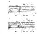
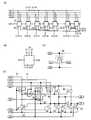
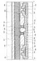
図1(A1)乃至(C)には同一基板上に作製された異なる構造の2つの薄膜トランジス
タの断面構造の一例を示す。図1(A1)乃至(C)に示す薄膜トランジスタ410は、
チャネルエッチ型と呼ばれるボトムゲート構造の一つであり、薄膜トランジスタ420は
チャネル保護型(チャネルストップ型ともいう)と呼ばれるボトムゲート構造の一つであ
る。薄膜トランジスタ410及び薄膜トランジスタ420は逆スタガ型薄膜トランジスタ
ともいう。FIGS. 1A1 to 1C illustrate an example of a cross-sectional structure of two thin film transistors with different structures manufactured over the same substrate. A
The
図1(A1)は駆動回路に配置されるチャネルエッチ型の薄膜トランジスタ410の平面
図であり、図1(B)は図1(A1)の線C1−C2における断面図である。また、図1
(C)は、図1(A1)の線C3−C4における断面図である。1A1 is a plan view of a channel-etched
FIG. 3C is a cross-sectional view taken along line C3-C4 in FIG.
駆動回路に配置される薄膜トランジスタ410はチャネルエッチ型の薄膜トランジスタで
あり、絶縁表面を有する基板400上に、ゲート電極層411、第1のゲート絶縁層40
2a、第2のゲート絶縁層402b、少なくともチャネル形成領域413、第1の高抵抗
ドレイン領域414a、及び第2の高抵抗ドレイン領域414bを有する酸化物半導体層
、ソース電極層415a、及びドレイン電極層415bを含む。また、薄膜トランジスタ
410を覆い、チャネル形成領域413に接する酸化物絶縁層416が設けられている。The
2a, a second
ソース電極層415aの下面に接して第1の高抵抗ドレイン領域414aが自己整合的に
形成されている。また、ドレイン電極層415bの下面に接して第2の高抵抗ドレイン領
域414bが自己整合的に形成されている。また、チャネル形成領域413は、酸化物絶
縁層416と接し、且つ膜厚が薄くなっており、第1の高抵抗ドレイン領域414a、及
び第2の高抵抗ドレイン領域414bよりも高抵抗の領域(I型領域)とする。A first high-
また、薄膜トランジスタ410は配線を低抵抗化するためにソース電極層415a、及び
ドレイン電極層415bとして金属材料を用いることが好ましい。The
また、液晶表示装置において、同一基板上に画素部と駆動回路を形成する場合、駆動回路
において、インバータ回路、NAND回路、NOR回路、ラッチ回路といった論理ゲート
を構成する薄膜トランジスタや、センスアンプ、定電圧発生回路、VCOといったアナロ
グ回路を構成する薄膜トランジスタは、ソース電極とドレイン電極間に正極性のみ、もし
くは負極性のみが印加される。従って、耐圧が要求される第2の高抵抗ドレイン領域41
4bの幅を第1の高抵抗ドレイン領域414aの幅よりも広く設計してもよい。また、第
1の高抵抗ドレイン領域414a、及び第2の高抵抗ドレイン領域414bがゲート電極
層と重なる幅を広くしてもよい。In a liquid crystal display device, when a pixel portion and a driver circuit are formed over the same substrate, a thin film transistor, a sense amplifier, a constant voltage, or the like that forms a logic gate such as an inverter circuit, a NAND circuit, a NOR circuit, or a latch circuit in the driver circuit. In a thin film transistor forming an analog circuit such as a generation circuit or a VCO, only positive polarity or only negative polarity is applied between a source electrode and a drain electrode. Therefore, the second high-
The width of 4b may be designed wider than the width of the first high
また、駆動回路に配置される薄膜トランジスタ410はシングルゲート構造の薄膜トラン
ジスタを用いて説明したが、必要に応じて、チャネル形成領域を複数有するマルチゲート
構造の薄膜トランジスタも形成することができる。Although the
また、チャネル形成領域413上方に重なる導電層417を設ける。導電層417をゲー
ト電極層411と電気的に接続し、同電位とすることで、ゲート電極層411と導電層4
17の間に配置された酸化物半導体層に上下からゲート電圧を印加することができる。ま
た、ゲート電極層411と導電層417を異なる電位、例えば固定電位、GND、0Vと
する場合には、TFTの電気特性、例えばしきい値電圧などを制御することができる。す
なわち、ゲート電極層411を第1のゲート電極層として機能させ、導電層417を第2
のゲート電極層として機能させることで、薄膜トランジスタ410を4端子の薄膜トラン
ジスタとして用いることができる。In addition, a
A gate voltage can be applied to the oxide semiconductor layer disposed between 17 from above and below. In the case where the
Thus, the
また、導電層417と酸化物絶縁層416の間には保護絶縁層403と、平坦化絶縁層4
04とを積層する。Further, a protective
04 is laminated.
また、保護絶縁層403は、保護絶縁層403の下方に設ける第1のゲート絶縁層402
aまたは下地となる絶縁膜と接する構成とすることが好ましく、基板の側面からの水分や
、水素イオンや、酸素イオンや、OH−などの不純物が侵入することをブロックする。特
に、保護絶縁層403と接する第1のゲート絶縁層402aまたは下地となる絶縁膜を窒
化珪素膜とすると有効である。The protective
It is preferable to be configured to be in contact with a or an insulating film serving as a base, and block entry of impurities such as moisture, hydrogen ions, oxygen ions, and OH− from the side surface of the substrate. In particular, it is effective that the first
また、図1(A2)は画素に配置されるチャネル保護型の薄膜トランジスタ420の平面
図であり、図1(B)は図1(A2)の線D1−D2における断面図である。また、図1
(C)は、図1(A2)の線D3−D4における断面図である。1A2 is a plan view of a channel protective
FIG. 3C is a cross-sectional view taken along line D3-D4 in FIG.
画素に配置される薄膜トランジスタ420はチャネル保護型の薄膜トランジスタであり、
絶縁表面を有する基板400上に、ゲート電極層421、第1のゲート絶縁層402a、
第2のゲート絶縁層402b、チャネル形成領域を含む酸化物半導体層422、チャネル
保護層として機能する酸化物絶縁層426、ソース電極層425a、及びドレイン電極層
425bを含む。また、薄膜トランジスタ420を覆い、酸化物絶縁層426、ソース電
極層425a、及びドレイン電極層425bに接して保護絶縁層403、及び平坦化絶縁
層404が積層して設けられている。平坦化絶縁層404上にはドレイン電極層425b
と接する画素電極層427が設けられており、薄膜トランジスタ420と電気的に接続し
ている。The
Over the
A second
Is provided, and is electrically connected to the
また、酸化物半導体膜の成膜以後に、不純物である水分などを低減する加熱処理(脱水化
または脱水素化のための加熱処理)が行われる。脱水化または脱水素化のための加熱処理
及び徐冷させた後、酸化物半導体層に接して酸化物絶縁膜の形成などを行って酸化物半導
体層のキャリア濃度を低減することが、薄膜トランジスタ420の電気特性の向上及び信
頼性の向上に繋がる。Further, after the oxide semiconductor film is formed, heat treatment (heat treatment for dehydration or dehydrogenation) that reduces moisture or the like which is an impurity is performed. The
画素に配置される薄膜トランジスタ420のチャネル形成領域は、酸化物半導体層422
のうち、チャネル保護層である酸化物絶縁層426に接し、且つゲート電極層421と重
なる領域である。薄膜トランジスタ420は、酸化物絶縁層426によって保護されるた
め、ソース電極層425a、ドレイン電極層425bを形成するエッチング工程で、酸化
物半導体層422がエッチングされるのを防ぐことができる。A channel formation region of the
Among these regions, the
また、薄膜トランジスタ420は透光性を有する薄膜トランジスタとして高開口率を有す
る表示装置を実現するためにソース電極層425a、ドレイン電極層425bは、透光性
を有する導電膜を用いる。The
また、薄膜トランジスタ420のゲート電極層421も透光性を有する導電膜を用いる。The
また、薄膜トランジスタ420が配置される画素には、画素電極層427、またはその他
の電極層(容量電極層など)や、その他の配線層(容量配線層など)に可視光に対して透
光性を有する導電膜を用い、高開口率を有する表示装置を実現する。勿論、第1のゲート
絶縁層402a、第2のゲート絶縁層402b、酸化物絶縁層426も可視光に対して透
光性を有する膜を用いることが好ましい。In addition, the pixel in which the
本明細書において、可視光に対して透光性を有する膜とは可視光の透過率が75〜100
%である膜厚を有する膜を指し、その膜が導電性を有する場合は透明の導電膜とも呼ぶ。
また、ゲート電極層、ソース電極層、ドレイン電極層、画素電極層、またはその他の電極
層や、その他の配線層に適用する金属酸化物として、可視光に対して半透明の導電膜を用
いてもよい。可視光に対して半透明とは可視光の透過率が50〜75%であることを指す
。In this specification, a film having a light-transmitting property with respect to visible light has a visible light transmittance of 75 to 100.
%, And when the film has conductivity, it is also called a transparent conductive film.
In addition, as a metal oxide applied to a gate electrode layer, a source electrode layer, a drain electrode layer, a pixel electrode layer, other electrode layers, or other wiring layers, a conductive film that is translucent to visible light is used. Also good. Translucent to visible light means that the visible light transmittance is 50 to 75%.
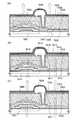
以下、図2及び図3(A)乃至(E)を用い、同一基板上に薄膜トランジスタ410及び
薄膜トランジスタ420を作製する工程を説明する。Hereinafter, a process of manufacturing the
まず、絶縁表面を有する基板400上に透光性を有する導電膜を形成した後、第1のフォ
トリソグラフィ工程によりゲート電極層411、421を形成する。また、画素部にはゲ
ート電極層411、421と同じ透光性を有する材料を用いて、第1のフォトリソグラフ
ィ工程により容量配線層を形成する。また、画素部だけでなく駆動回路に容量が必要な場
合には、駆動回路にも容量配線層を形成する。なお、レジストマスクをインクジェット法
で形成してもよい。レジストマスクをインクジェット法で形成するとフォトマスクを使用
しないため、製造コストを低減できる。First, after a light-transmitting conductive film is formed over the
絶縁表面を有する基板400に使用することができる基板に大きな制限はないが、少なく
とも、後の加熱処理に耐えうる程度の耐熱性を有していることが必要となる。絶縁表面を
有する基板400にはバリウムホウケイ酸ガラスやアルミノホウケイ酸ガラスなどのガラ
ス基板を用いることができる。There is no particular limitation on a substrate that can be used as the
また、基板400としては、後の加熱処理の温度が高い場合には、歪み点が730℃以上
のものを用いると良い。また、ガラス基板には、例えば、アルミノシリケートガラス、ア
ルミノホウケイ酸ガラス、バリウムホウケイ酸ガラスなどのガラス材料が用いられている
。なお、ホウ酸と比較して酸化バリウム(BaO)を多く含ませることで、より実用的な
耐熱ガラスが得られる。このため、B2O3よりBaOを多く含むガラス基板を用いるこ
とが好ましい。As the
なお、上記のガラス基板に代えて、セラミック基板、石英基板、サファイア基板などの絶
縁体でなる基板を用いても良い。他にも、結晶化ガラスなどを用いることができる。Note that a substrate formed of an insulator such as a ceramic substrate, a quartz substrate, or a sapphire substrate may be used instead of the glass substrate. In addition, crystallized glass or the like can be used.
また、下地膜となる絶縁膜を基板400とゲート電極層411、421の間に設けてもよ
い。下地膜は、基板400からの不純物元素の拡散を防止する機能があり、窒化珪素膜、
酸化珪素膜、窒化酸化珪素膜、又は酸化窒化珪素膜から選ばれた一又は複数の膜による積
層構造により形成することができる。An insulating film serving as a base film may be provided between the
It can be formed with a stacked structure of one or more films selected from a silicon oxide film, a silicon nitride oxide film, and a silicon oxynitride film.
ゲート電極層411、421の材料は、可視光に対して透光性を有する導電材料、例えば
In−Sn−Zn−O系、In−Al−Zn−O系、Sn−Ga−Zn−O系、Al−G
a−Zn−O系、Sn−Al−Zn−O系、In−Zn−O系、Sn−Zn−O系、Al
−Zn−O系、In−O系、Sn−O系、Zn−O系の金属酸化物を適用することができ
、膜厚は50nm以上300nm以下の範囲内で適宜選択する。ゲート電極層411、4
21に用いる金属酸化物の成膜方法は、スパッタ法や真空蒸着法(電子ビーム蒸着法など
)や、アーク放電イオンプレーティング法や、スプレー法を用いる。また、スパッタ法を
用いる場合、SiO2を2重量%以上10重量%以下含むターゲットを用いて成膜を行い
、透光性を有する導電膜に結晶化を阻害するSiOx(X>0)を含ませ、後の工程で行
う脱水化または脱水素化のための加熱処理の際に結晶化してしまうのを抑制することが好
ましい。The material of the gate electrode layers 411 and 421 is a conductive material having a property of transmitting visible light, such as an In—Sn—Zn—O-based material, an In—Al—Zn—O-based material, or a Sn—Ga—Zn—O-based material. , Al-G
a-Zn-O, Sn-Al-Zn-O, In-Zn-O, Sn-Zn-O, Al
A —Zn—O-based, In—O-based, Sn—O-based, or Zn—O-based metal oxide can be used, and the film thickness is appropriately selected within a range of 50 nm to 300 nm. Gate electrode layers 411, 4
As a method for forming a
次いで、ゲート電極層411、421上にゲート絶縁層を形成する。Next, a gate insulating layer is formed over the gate electrode layers 411 and 421.
ゲート絶縁層は、プラズマCVD法又はスパッタリング法等を用いて、酸化珪素層、窒化
珪素層、酸化窒化珪素層又は窒化酸化珪素層を単層で又は積層して形成することができる
。例えば、成膜ガスとして、SiH4、酸素及び窒素を用いてプラズマCVD法により酸
化窒化珪素層を形成すればよい。The gate insulating layer can be formed as a single layer or a stack of silicon oxide layers, silicon nitride layers, silicon oxynitride layers, or silicon nitride oxide layers by a plasma CVD method, a sputtering method, or the like. For example, a silicon oxynitride layer may be formed by a plasma CVD method using SiH4 , oxygen, and nitrogen as a deposition gas.
本実施の形態では、膜厚50nm以上200nm以下の第1のゲート絶縁層402aと、
膜厚50nm以上300nm以下の第2のゲート絶縁層402bの積層のゲート絶縁層と
する。第1のゲート絶縁層402aとしては膜厚100nmの窒化珪素膜または窒化酸化
珪素膜を用いる。また、第2のゲート絶縁層402bとしては、膜厚100nmの酸化珪
素膜を用いる。In this embodiment, a first
The gate insulating layer is a stack of the second
第2のゲート絶縁層402b上に、膜厚2nm以上200nm以下の酸化物半導体膜43
0を形成する。酸化物半導体膜430の形成後に脱水化または脱水素化のための加熱処理
を行っても酸化物半導体膜を非晶質な状態とするため、膜厚を50nm以下と薄くするこ
とが好ましい。酸化物半導体膜の膜厚を薄くすることで酸化物半導体層の形成後に加熱処
理した場合に、結晶化してしまうのを抑制することができる。An
0 is formed. Even when heat treatment for dehydration or dehydrogenation is performed after the formation of the
なお、酸化物半導体膜430をスパッタ法により成膜する前に、アルゴンガスを導入して
プラズマを発生させる逆スパッタを行い、第2のゲート絶縁層402bの表面に付着して
いるゴミを除去することが好ましい。逆スパッタとは、ターゲット側に電圧を印加せずに
、アルゴン雰囲気下で基板側にRF電源を用いて電圧を印加して基板近傍にプラズマを形
成して表面を改質する方法である。なお、アルゴン雰囲気に代えて窒素、ヘリウム、酸素
などを用いてもよい。Note that before the
酸化物半導体膜430は、In−Ga−Zn−O系非単結晶膜、In−Sn−Zn−O系
、In−Al−Zn−O系、Sn−Ga−Zn−O系、Al−Ga−Zn−O系、Sn−
Al−Zn−O系、In−Zn−O系、Sn−Zn−O系、Al−Zn−O系、In−O
系、Sn−O系、Zn−O系の酸化物半導体膜を用いる。本実施の形態では、In−Ga
−Zn−O系酸化物半導体ターゲットを用いてスパッタ法により成膜する。また、酸化物
半導体膜430は、希ガス(代表的にはアルゴン)雰囲気下、酸素雰囲気下、又は希ガス
(代表的にはアルゴン)及び酸素雰囲気下においてスパッタ法により形成することができ
る。また、スパッタ法を用いる場合、SiO2を2重量%以上10重量%以下含むターゲ
ットを用いて成膜を行い、酸化物半導体膜430に結晶化を阻害するSiOx(X>0)
を含ませ、後の工程で行う脱水化または脱水素化のための加熱処理の際に結晶化してしま
うのを抑制することが好ましい。The
Al-Zn-O, In-Zn-O, Sn-Zn-O, Al-Zn-O, In-O
, Sn—O, and Zn—O-based oxide semiconductor films are used. In this embodiment, In—Ga
A film is formed by a sputtering method using a —Zn—O-based oxide semiconductor target. The
It is preferable to suppress crystallization during heat treatment for dehydration or dehydrogenation performed in a later step.
また、酸化物半導体膜は、好ましくはInを含有する酸化物半導体、さらに好ましくは、
In、及びGaを含有する酸化物半導体膜である。酸化物半導体膜をI型(真性)とする
ため、脱水化または脱水素化は有効である。The oxide semiconductor film is preferably an oxide semiconductor containing In, more preferably
It is an oxide semiconductor film containing In and Ga. Since the oxide semiconductor film is i-type (intrinsic), dehydration or dehydrogenation is effective.
次いで、酸化物半導体膜430を第2のフォトリソグラフィ工程により島状の酸化物半導
体層に加工する。また、島状の酸化物半導体層を形成するためのレジストマスクをインク
ジェット法で形成してもよい。レジストマスクをインクジェット法で形成するとフォトマ
スクを使用しないため、製造コストを低減できる。Next, the
次いで、酸化物半導体層の脱水化または脱水素化を行う。脱水化または脱水素化を行う第
1の加熱処理の温度は、350℃以上基板の歪み点未満、好ましくは400℃以上とする
。ここでは、加熱処理装置の一つである電気炉に基板を導入し、酸化物半導体層に対して
窒素雰囲気下において加熱処理を行った後、大気に触れることなく、酸化物半導体層への
水や水素の再混入を防ぎ、酸化物半導体層431、432を得る(図2(B)参照。)。
本実施の形態では、酸化物半導体層の脱水化または脱水素化を行う加熱温度Tから、再び
水が入らないような十分な温度まで同じ炉を用い、具体的には加熱温度Tよりも100℃
以上下がるまで窒素雰囲気下で徐冷する。また、窒素雰囲気に限定されず、ヘリウム、ネ
オン、アルゴンの希ガス雰囲気下或いは減圧下において脱水化または脱水素化を行う。Next, dehydration or dehydrogenation of the oxide semiconductor layer is performed. The temperature of the first heat treatment for dehydration or dehydrogenation is 350 ° C. or higher and lower than the strain point of the substrate, preferably 400 ° C. or higher. Here, a substrate is introduced into an electric furnace which is one of heat treatment apparatuses, and heat treatment is performed on the oxide semiconductor layer in a nitrogen atmosphere. And re-mixing of hydrogen and the oxide semiconductor layers 431 and 432 are obtained (see FIG. 2B).
In this embodiment, the same furnace is used from the heating temperature T at which the oxide semiconductor layer is dehydrated or dehydrogenated to a sufficient temperature so that water does not enter again. ℃
Slowly cool in a nitrogen atmosphere until the temperature drops. Further, without limitation to a nitrogen atmosphere, dehydration or dehydrogenation is performed in a rare gas atmosphere of helium, neon, or argon or under reduced pressure.
なお、第1の加熱処理においては、窒素、またはヘリウム、ネオン、アルゴン等の希ガス
に、水、水素などが含まれないことが好ましい。または、加熱処理装置に導入する窒素、
またはヘリウム、ネオン、アルゴン等の希ガスの純度を、6N(99.9999%)以上
、好ましくは7N(99.99999%)以上、(即ち不純物濃度を1ppm以下、好ま
しくは0.1ppm以下)とすることが好ましい。Note that in the first heat treatment, it is preferable that water, hydrogen, or the like be not contained in nitrogen or a rare gas such as helium, neon, or argon. Or nitrogen introduced into the heat treatment apparatus,
Alternatively, the purity of a rare gas such as helium, neon, or argon is 6N (99.9999%) or more, preferably 7N (99.99999%) or more (that is, the impurity concentration is 1 ppm or less, preferably 0.1 ppm or less). It is preferable to do.
また、第1の加熱処理の条件、または酸化物半導体膜の材料によっては、結晶化し、微結
晶膜または多結晶膜となる場合もある。Further, depending on the conditions of the first heat treatment or the material of the oxide semiconductor film, it may crystallize into a microcrystalline film or a polycrystalline film.
また、酸化物半導体層の第1の加熱処理は、島状の酸化物半導体層に加工する前の酸化物
半導体膜430に行うこともできる。その場合には、第1の加熱処理後に、加熱装置から
基板を取り出し、フォトリソグラフィ工程を行う。The first heat treatment of the oxide semiconductor layer can be performed on the
また、酸化物半導体膜430の成膜前に、不活性ガス雰囲気(窒素、またはヘリウム、ネ
オン、アルゴン等)下、酸素雰囲気、或いは減圧下において加熱処理(400℃以上基板
の歪み点未満)を行い、ゲート絶縁層内に含まれる水素及び水などの不純物を除去しても
よい。Further, before the
次いで、第2のゲート絶縁層402b、及び酸化物半導体層431、432上に、金属導
電膜を形成した後、第3のフォトリソグラフィ工程によりレジストマスク433a、43
3bを形成し、選択的にエッチングを行って金属電極層434、435を形成する(図2
(C)参照)。金属導電膜の材料としては、Al、Cr、Cu、Ta、Ti、Mo、Wか
ら選ばれた元素、または上述した元素を成分とする合金か、上述した元素を組み合わせた
合金等がある。Next, after a metal conductive film is formed over the second
3b is formed and selectively etched to form metal electrode layers 434 and 435 (FIG. 2).
(See (C)). Examples of the material for the metal conductive film include an element selected from Al, Cr, Cu, Ta, Ti, Mo, and W, an alloy containing the above-described element as a component, or an alloy combining the above-described elements.
金属導電膜としては、チタン層上にアルミニウム層と、該アルミニウム層上にチタン層が
積層された三層の積層構造、またはモリブデン層上にアルミニウム層と、該アルミニウム
層上にモリブデン層を積層した三層の積層構造とすることが好ましい。勿論、金属導電膜
として単層、または2層構造、または4層以上の積層構造としてもよい。As the metal conductive film, an aluminum layer on the titanium layer and a three-layer structure in which the titanium layer is laminated on the aluminum layer, or an aluminum layer on the molybdenum layer and a molybdenum layer on the aluminum layer are laminated. A three-layer structure is preferable. Of course, the metal conductive film may have a single layer, a two-layer structure, or a stacked structure of four or more layers.
また、金属電極層434、435を形成するためのレジストマスクをインクジェット法で
形成してもよい。レジストマスクをインクジェット法で形成するとフォトマスクを使用し
ないため、製造コストを低減できる。Further, a resist mask for forming the metal electrode layers 434 and 435 may be formed by an inkjet method. When the resist mask is formed by an ink-jet method, a manufacturing cost can be reduced because a photomask is not used.
次いで、レジストマスク433a、433bを除去し、第4のフォトリソグラフィ工程に
よりレジストマスク436a、436bを形成し、選択的にエッチングを行ってソース電
極層415a、及びドレイン電極層415bを形成する(図2(D)参照)。なお、第4
のフォトリソグラフィ工程では、酸化物半導体層431は一部のみがエッチングされ、溝
部(凹部)を有する酸化物半導体層437となる。また、酸化物半導体層431に溝部(
凹部)を形成するためのレジストマスク436a、436bをインクジェット法で形成し
てもよい。レジストマスクをインクジェット法で形成するとフォトマスクを使用しないた
め、製造コストを低減できる。Next, the resist
In this photolithography step, only part of the
Resist
次いで、レジストマスク436a、436bを除去し、第5のフォトリソグラフィ工程に
より酸化物半導体層437を覆うレジストマスク438を形成し、酸化物半導体層432
上の金属電極層435を除去する(図2(E)参照。)。Next, the resist
The upper
なお、第5のフォトリソグラフィ工程で酸化物半導体層432と重なる金属電極層435
を除去するため、金属電極層435のエッチングの際に、酸化物半導体層432も除去さ
れないようにそれぞれの材料及びエッチング条件を適宜調節する。Note that the
In order to remove the
酸化物半導体層432の上面及び側面に接し、酸化物半導体層437の溝部(凹部)に接
する保護絶縁膜となる酸化物絶縁膜439を形成する。An
酸化物絶縁膜439は、少なくとも1nm以上の膜厚とし、スパッタリング法など、酸化
物絶縁膜439に水、水素等の不純物を混入させない方法を適宜用いて形成することがで
きる。本実施の形態では、酸化物絶縁膜439として膜厚300nmの酸化珪素膜をスパ
ッタリング法を用いて成膜する。成膜時の基板温度は、室温以上300℃以下とすればよ
く、本実施の形態では100℃とする。酸化珪素膜のスパッタリング法による成膜は、希
ガス(代表的にはアルゴン)雰囲気下、酸素雰囲気下、または希ガス(代表的にはアルゴ
ン)及び酸素雰囲気下において行うことができる。また、ターゲットとして酸化珪素ター
ゲットまたは珪素ターゲットを用いることができる。例えば、珪素ターゲットを用いて、
酸素、及び窒素雰囲気下でスパッタリング法により酸化珪素を形成することができる。低
抵抗化した酸化物半導体層に接して形成する酸化物絶縁膜439は、水分や、水素イオン
や、酸素イオンや、OH−などの不純物を含まず、これらが外部から侵入することをブロ
ックする無機絶縁膜を用い、代表的には酸化珪素膜、窒化酸化珪素膜、酸化アルミニウム
膜、または酸化窒化アルミニウムなどを用いる。The
Silicon oxide can be formed by a sputtering method in an atmosphere containing oxygen and nitrogen. The
次いで、不活性ガス雰囲気下、または酸素ガス雰囲気下で第2の加熱処理(好ましくは2
00℃以上400℃以下、例えば250℃以上350℃以下)を行う(図3(A)参照。
)。例えば、窒素雰囲気下で250℃、1時間の第2の加熱処理を行う。第2の加熱処理
を行うと、酸化物半導体層437の溝部、酸化物半導体層432の上面及び側面が酸化物
絶縁膜439と接した状態で加熱される。Next, a second heat treatment (preferably 2) is performed in an inert gas atmosphere or an oxygen gas atmosphere.
00 ° C. or more and 400 ° C. or less, for example, 250 ° C. or more and 350 ° C. or less) (see FIG. 3A).
). For example, the second heat treatment is performed at 250 ° C. for 1 hour in a nitrogen atmosphere. When the second heat treatment is performed, the groove of the
以上の工程を経ることによって、成膜後の酸化物半導体膜に対して脱水化または脱水素化
のための加熱処理を行って低抵抗化した後、酸化物半導体膜の一部を選択的に酸素過剰な
状態とする。その結果、ゲート電極層411と重なるチャネル形成領域413は、I型と
なり、ソース電極層415aに重なる第1の高抵抗ドレイン領域414aと、ドレイン電
極層415bに重なる第2の高抵抗ドレイン領域414bとが自己整合的に形成される。
また、ゲート電極層421と重なる酸化物半導体層422は、全体がI型となる。Through the above steps, the oxide semiconductor film after film formation is subjected to heat treatment for dehydration or dehydrogenation to reduce resistance, and then part of the oxide semiconductor film is selectively formed. Make oxygen excess. As a result, the
In addition, the
しかし、高抵抗化された(I型化された)酸化物半導体層422が露出している状態で、
窒素、不活性ガス雰囲気下、又は減圧下で加熱処理を行うと、高抵抗化された(I型化さ
れた)酸化物半導体層422が低抵抗化してしまうため、酸化物半導体層422が露出し
ている状態で行う加熱処理は酸素ガス、N2Oガス雰囲気下、又は、超乾燥エア(露点が
−40℃以下、好ましくは−60℃以下)で行う。However, in a state where the
When heat treatment is performed in an atmosphere of nitrogen, an inert gas, or reduced pressure, the resistance of the
ドレイン電極層415b(及びソース電極層415a)と重畳した酸化物半導体層におい
て第2の高抵抗ドレイン領域414b(又は第1の高抵抗ドレイン領域414a)を形成
することにより、駆動回路を形成した際の信頼性の向上を図ることができる。具体的には
、第2の高抵抗ドレイン領域414bを形成することで、ドレイン電極層から第2の高抵
抗ドレイン領域414b、チャネル形成領域にかけて、導電性を段階的に変化させうるよ
うな構造とすることができる。そのため、ドレイン電極層415bを高電源電位VDDを
供給する配線に接続して動作させる場合、ゲート電極層411とドレイン電極層415b
との間に高電界が印加されても高抵抗ドレイン領域がバッファとなり局所的な高電界が印
加されず、トランジスタの耐圧を向上させた構成とすることができる。When the driver circuit is formed by forming the second high-
Even if a high electric field is applied between them, the high-resistance drain region becomes a buffer and a local high electric field is not applied, so that the withstand voltage of the transistor can be improved.
また、ドレイン電極層415b(及びソース電極層415a)と重畳した酸化物半導体層
において第2の高抵抗ドレイン領域414b(又は第1の高抵抗ドレイン領域414a)
を形成することにより、駆動回路を形成した際のチャネル形成領域413でのリーク電流
の低減を図ることができる。Further, in the oxide semiconductor layer overlapping with the
Thus, leakage current in the
次いで、第6のフォトリソグラフィ工程により、レジストマスク440a、440bを形
成し、酸化物絶縁膜439を選択的にエッチングして、酸化物絶縁層416、426を形
成する(図3(B)参照。)。酸化物絶縁層426は酸化物半導体層422のチャネル形
成領域上に設けられ、チャネル保護層として機能する。なお、本実施の形態のように、ゲ
ート絶縁層402bとして酸化物絶縁層を用いる場合、酸化物絶縁膜439のエッチング
工程により、ゲート絶縁層402bの一部もエッチングされて膜厚が薄くなる(膜減りす
る)場合がある。ゲート絶縁層402bとして酸化物絶縁膜439と選択比の高い窒化絶
縁膜を用いる場合は、ゲート絶縁層402bが一部エッチングされるのを防ぐことができ
る。Next, resist
次いで、酸化物半導体層422及び酸化物絶縁層426上に、透光性を有する導電膜を形
成した後、第7のフォトリソグラフィ工程によりソース電極層425a、及びドレイン電
極層425bを形成する(図3(C)参照。)。透光性を有する導電膜の成膜方法は、ス
パッタ法や真空蒸着法(電子ビーム蒸着法など)や、アーク放電イオンプレーティング法
や、スプレー法を用いる。導電膜の材料としては、可視光に対して透光性を有する導電材
料、例えばIn−Sn−Zn−O系、In−Al−Zn−O系、Sn−Ga−Zn−O系
、Al−Ga−Zn−O系、Sn−Al−Zn−O系、In−Zn−O系、Sn−Zn−
O系、Al−Zn−O系、In−O系、Sn−O系、Zn−O系の金属酸化物を適用する
ことができ、膜厚は50nm以上300nm以下の範囲内で適宜選択する。また、スパッ
タ法を用いる場合、SiO2を2重量%以上10重量%以下含むターゲットを用いて成膜
を行い、透光性を有する導電膜に結晶化を阻害するSiOx(X>0)を含ませ、後の工
程で加熱処理を行う際に結晶化してしまうのを抑制することが好ましい。Next, a light-transmitting conductive film is formed over the
An O-based, Al-Zn-O-based, In-O-based, Sn-O-based, or Zn-O-based metal oxide can be used, and the film thickness is appropriately selected within the range of 50 nm to 300 nm. In addition, in the case of using a sputtering method, a film containing a SiO2 target of 2 wt% to 10 wt% is formed, and the light-transmitting conductive film contains SiO x (X> 0) that inhibits crystallization. However, it is preferable to suppress crystallization when heat treatment is performed in a later step.
なお、ソース電極層425a、ドレイン電極層425bを形成するためのレジストマスク
をインクジェット法で形成してもよい。レジストマスクをインクジェット法で形成すると
フォトマスクを使用しないため、製造コストを低減できる。Note that a resist mask for forming the
次いで、酸化物絶縁層416、426、ソース電極層425a、ドレイン電極層425b
上に保護絶縁層403を形成する。本実施の形態では、RFスパッタ法を用いて窒化珪素
膜を形成する。RFスパッタ法は、量産性がよいため、保護絶縁層403の成膜方法とし
て好ましい。保護絶縁層403は、水分や、水素イオンや、OH−などの不純物を含まず
、これらが外部から侵入することをブロックする無機絶縁膜を用い、窒化珪素膜、窒化ア
ルミニウム膜、窒化酸化珪素膜、酸化窒化アルミニウムなどを用いる。勿論、保護絶縁層
403は透光性を有する絶縁膜である。Next, the
A protective insulating
また、保護絶縁層403は、保護絶縁層403の下方に設ける第1のゲート絶縁層402
aまたは下地となる絶縁膜と接する構成とすることが好ましく、基板の側面近傍からの水
分や、水素イオンや、OH−などの不純物が侵入することをブロックする。特に、保護絶
縁層403と接する第1のゲート絶縁層402aまたは下地となる絶縁膜を窒化珪素膜と
すると有効である。即ち、酸化物半導体層の下面、上面、及び側面を囲むように窒化珪素
膜を設けると、表示装置の信頼性が向上する。The protective
It is preferable to be configured to be in contact with a or an insulating film serving as a base, and to block entry of moisture, hydrogen ions, impurities such as OH− from the vicinity of the side surface of the substrate. In particular, it is effective that the first
次いで、保護絶縁層403上に平坦化絶縁層404を形成する。平坦化絶縁層404とし
ては、ポリイミド、アクリル、ベンゾシクロブテン、ポリアミド、エポキシ等の、耐熱性
を有する有機材料を用いることができる。また上記有機材料の他に、低誘電率材料(lo
w−k材料)、シロキサン系樹脂、PSG(リンガラス)、BPSG(リンボロンガラス
)等を用いることができる。なお、これらの材料で形成される絶縁膜を複数積層させるこ
とで、平坦化絶縁層404を形成してもよい。Next, a
wk material), siloxane-based resin, PSG (phosphorus glass), BPSG (phosphorus boron glass), or the like can be used. Note that the
なおシロキサン系樹脂とは、シロキサン系材料を出発材料として形成されたSi−O−S
i結合を含む樹脂に相当する。シロキサン系樹脂は置換基としては有機基(例えばアルキ
ル基やアリール基)やフルオロ基を用いても良い。また、有機基はフルオロ基を有してい
ても良い。Note that the siloxane-based resin is Si—O—S formed using a siloxane-based material as a starting material.
It corresponds to a resin containing i-bond. Siloxane resins may use organic groups (for example, alkyl groups and aryl groups) and fluoro groups as substituents. The organic group may have a fluoro group.
平坦化絶縁層404の形成法は、特に限定されず、その材料に応じて、スパッタ法、SO
G法、スピンコート、ディップ、スプレー塗布、液滴吐出法(インクジェット法、スクリ
ーン印刷、オフセット印刷等)等の方法や、ドクターナイフ、ロールコーター、カーテン
コーター、ナイフコーター等を用いることができる。There is no particular limitation on the formation method of the
Methods such as G method, spin coating, dipping, spray coating, droplet discharge method (ink jet method, screen printing, offset printing, etc.), doctor knife, roll coater, curtain coater, knife coater, etc. can be used.
次に、第8のフォトリソグラフィ工程を行い、レジストマスクを形成し、平坦化絶縁層4
04、及び保護絶縁層403のエッチングによりドレイン電極層425bに達するコンタ
クトホール441を形成する(図3(D)参照。)。また、ここでのエッチングによりゲ
ート電極層411、421に達するコンタクトホールも形成する。また、ドレイン電極層
425bに達するコンタクトホールを形成するためのレジストマスクをインクジェット法
で形成してもよい。レジストマスクをインクジェット法で形成するとフォトマスクを使用
しないため、製造コストを低減できる。Next, an eighth photolithography step is performed to form a resist mask, and the
04 and the protective insulating
次いで、レジストマスクを除去した後、透光性を有する導電膜を成膜する。透光性を有す
る導電膜の材料としては、酸化インジウム(In2O3)や酸化インジウム酸化スズ合金
(In2O3―SnO2、ITOと略記する)などをスパッタ法や真空蒸着法などを用い
て形成する。透光性を有する導電膜の他の材料として、窒素を含ませたAl−Zn−O系
非単結晶膜、即ちAl−Zn−O−N系非単結晶膜や、窒素を含ませたZn−O系非単結
晶膜や、窒素を含ませたSn−Zn−O系非単結晶膜を用いてもよい。なお、Al−Zn
−O−N系非単結晶膜の亜鉛の組成比(原子%)は、47原子%以下とし、非単結晶膜中
のアルミニウムの組成比(原子%)より大きく、非単結晶膜中のアルミニウムの組成比(
原子%)は、非単結晶膜中の窒素の組成比(原子%)より大きい。このような材料のエッ
チング処理は塩酸系の溶液により行う。しかし、特にITOのエッチングは残渣が発生し
やすいので、エッチング加工性を改善するために酸化インジウム酸化亜鉛合金(In2O
3―ZnO)を用いても良い。Next, after removing the resist mask, a light-transmitting conductive film is formed. As a material for the light-transmitting conductive film, indium oxide (In2 O3 ), indium tin oxide alloy (In2 O3 —SnO2 , abbreviated as ITO), or the like is formed by sputtering or vacuum evaporation. Use to form. As another material for the light-transmitting conductive film, an Al—Zn—O-based non-single-crystal film containing nitrogen, that is, an Al—Zn—O—N-based non-single-crystal film, or Zn containing nitrogen A —O-based non-single-crystal film or a Sn—Zn—O-based non-single-crystal film containing nitrogen may be used. Al-Zn
The composition ratio (atomic%) of zinc in the —O—N-based non-single-crystal film is 47 atomic% or less, which is larger than the composition ratio (atomic%) of aluminum in the non-single-crystal film. Composition ratio (
(Atomic%) is larger than the composition ratio (atomic%) of nitrogen in the non-single crystal film. Etching treatment of such a material is performed with a hydrochloric acid based solution. However, in particular, etching of ITO tends to generate a residue, so in order to improve etching processability, an indium oxide-zinc oxide alloy (In2 O
3- ZnO) may be used.
なお、透光性を有する導電膜の組成比の単位は原子%とし、電子線マイクロアナライザー
(EPMA:Electron Probe X−ray MicroAnalyzer
)を用いた分析により評価するものとする。Note that the unit of the composition ratio of the light-transmitting conductive film is atomic%, and an electron probe microanalyzer (EPMA: Electron Probe X-ray Micro Analyzer).
).
次に、第9のフォトリソグラフィ工程を行い、レジストマスクを形成し、エッチングによ
り不要な部分を除去して画素電極層427及び導電層417を形成する(図3(E)参照
。)。Next, a ninth photolithography step is performed to form a resist mask, and unnecessary portions are removed by etching, so that the
以上の工程により、9枚のマスクを用いて、同一基板上に薄膜トランジスタ410及び薄
膜トランジスタ420をそれぞれ駆動回路または画素部に作り分けて作製することができ
る。駆動回路用の薄膜トランジスタ410は、第1の高抵抗ドレイン領域414a、第2
の高抵抗ドレイン領域414b、及びチャネル形成領域413を含む酸化物半導体層41
2を含むチャネルエッチ型薄膜トランジスタであり、画素用の薄膜トランジスタ420は
、全体がI型化した酸化物半導体層422を含むチャネル保護型薄膜トランジスタである
。Through the above process, the
The pixel
また、第1のゲート絶縁層402a、第2のゲート絶縁層402bを誘電体とし容量配線
層と容量電極とで形成される保持容量も同一基板上に形成することができる。薄膜トラン
ジスタ420と保持容量を個々の画素に対応してマトリクス状に配置して画素部を構成し
、画素部の周辺に薄膜トランジスタ410を有する駆動回路を配置することによりアクテ
ィブマトリクス型の表示装置を作製するための一方の基板とすることができる。本明細書
では便宜上このような基板をアクティブマトリクス基板と呼ぶ。In addition, a storage capacitor formed using a capacitor wiring layer and a capacitor electrode using the first
なお、画素電極層427は、平坦化絶縁層404、及び保護絶縁層403に形成されたコ
ンタクトホールを介して容量電極と電気的に接続する。なお、容量電極は、ソース電極層
425a、ドレイン電極層425bと同じ透光性を有する材料、同じ工程で形成すること
ができる。Note that the
導電層417を酸化物半導体層のチャネル形成領域413と重なる位置に設けることによ
って、薄膜トランジスタの信頼性を調べるためのバイアス−熱ストレス試験(以下、BT
試験という)において、BT試験前後における薄膜トランジスタ410のしきい値電圧の
変化量を低減することができる。また、導電層417は、電位がゲート電極層411と同
じでもよいし、異なっていても良く、第2のゲート電極層として機能させることもできる
。また、導電層417の電位がGND、0V、或いはフローティング状態であってもよい
。By providing the
In the test), the amount of change in the threshold voltage of the
また、画素電極層427を形成するためのレジストマスクをインクジェット法で形成して
もよい。レジストマスクをインクジェット法で形成するとフォトマスクを使用しないため
、製造コストを低減できる。Further, a resist mask for forming the
(実施の形態2)
本実施の形態では、画素用薄膜トランジスタにおいて加熱処理が実施の形態1と異なる例
を図4に示す。図4は、図1乃至図3と工程が一部異なる点以外は同じであるため、同じ
箇所には同じ符号を用い、同じ箇所の詳細な説明は省略する。(Embodiment 2)
In this embodiment mode, FIG. 4 shows an example in which the heat treatment in the pixel thin film transistor is different from that in
まず、実施の形態1に従って、実施の形態1における図3(B)の工程まで行う。図4(
A)は、図3(B)の工程後、レジストマスク440a、440bを除去した状態である
。First, according to
FIG. 3A shows a state in which the resist
絶縁表面を有する基板400上に、ゲート電極層411、421、第1のゲート絶縁層4
02a、第2のゲート絶縁層402bが形成され、駆動回路部においてはチャネル形成領
域413、第1の高抵抗ドレイン領域414a、第2の高抵抗ドレイン領域414bを含
む酸化物半導体層412、ソース電極層415a、ドレイン電極層415b、酸化物絶縁
層416が形成され、画素部においては酸化物半導体層422、酸化物絶縁層426が形
成されている(図4(A)参照。)。酸化物半導体層422は高抵抗化されたI型である
。On the
02a, a second
本実施の形態では、少なくとも酸化物半導体層422の一部が露出している状態で、窒素
、不活性ガス雰囲気下、又は減圧下で加熱処理を行う。高抵抗化された(I型化された)
酸化物半導体層422が露出している状態で、窒素、不活性ガス雰囲気下、又は減圧下で
加熱処理を行うと、酸化物半導体層422において露出している高抵抗化された(I型化
された)領域が低抵抗化することができる。In this embodiment, heat treatment is performed in a nitrogen or inert gas atmosphere or under reduced pressure with at least part of the
When heat treatment is performed in an atmosphere of nitrogen, an inert gas, or reduced pressure with the
酸化物半導体層422において、高抵抗化された(I型化された)領域を低抵抗化する加
熱処理は、好ましくは200℃以上400℃以下、例えば250℃以上350℃以下で行
えばよい。例えば、窒素雰囲気下で250℃、1時間の加熱処理を行う。In the
本実施の形態では、加熱処理装置の一つである電気炉に基板を導入し、酸化物半導体層4
22に対して窒素雰囲気下において加熱処理を行った後、大気に触れることなく、加熱温
度Tから、加熱温度Tよりも100℃以上下がるまで窒素雰囲気下で徐冷する。また、窒
素雰囲気に限定されず、ヘリウム、ネオン、アルゴン等の希ガス雰囲気下或いは減圧下に
おいて脱水化または脱水素化を行う。なお、加熱処理においては、窒素、またはヘリウム
、ネオン、アルゴン等の希ガスに、水、水素などが含まれないことが好ましい。または、
加熱処理装置に導入する窒素、またはヘリウム、ネオン、アルゴン等の希ガスの純度を、
6N(99.9999%)以上、好ましくは7N(99.99999%)以上、(即ち不
純物濃度を1ppm以下、好ましくは0.1ppm以下)とすることが好ましい。In this embodiment, a substrate is introduced into an electric furnace which is one of heat treatment apparatuses, and the
After heat-treating 22 in a nitrogen atmosphere, it is gradually cooled in a nitrogen atmosphere from the heating temperature T until the temperature falls by 100 ° C. or more from the heating temperature T without touching the air. Further, the present invention is not limited to a nitrogen atmosphere, and dehydration or dehydrogenation is performed in a rare gas atmosphere such as helium, neon, or argon, or under reduced pressure. Note that in the heat treatment, it is preferable that water, hydrogen, or the like be not contained in nitrogen or a rare gas such as helium, neon, or argon. Or
The purity of nitrogen or a rare gas such as helium, neon, or argon introduced into the heat treatment apparatus,
6N (99.9999%) or more, preferably 7N (99.99999%) or more (that is, the impurity concentration is 1 ppm or less, preferably 0.1 ppm or less).
酸化物半導体層422に対する窒素、不活性ガス雰囲気下、又は減圧下での加熱処理によ
って、酸化物半導体層422の露出領域は低抵抗化し、抵抗の異なる領域(図4(B)に
おいては斜線領域及び白地領域で示す)を有する酸化物半導体層442となる。The exposed region of the
次いで、酸化物半導体層442及び酸化物絶縁層426上に、透光性を有する導電膜を形
成した後、第7のフォトリソグラフィ工程によりソース電極層425a、及びドレイン電
極層425bを形成する(図4(C)参照。)。Next, a light-transmitting conductive film is formed over the
次いで、酸化物絶縁層416、426、ソース電極層425a、ドレイン電極層425b
上に保護絶縁層403、平坦化絶縁層404を積層して形成する。Next, the
A protective insulating
次に、第8のフォトリソグラフィ工程を行い、レジストマスクを形成し、平坦化絶縁層4
04、及び保護絶縁層403のエッチングによりドレイン電極層425bに達するコンタ
クトホール441を形成する(図4(D)参照。)。Next, an eighth photolithography step is performed to form a resist mask, and the
04 and the protective insulating
次いで、レジストマスクを除去した後、透光性を有する導電膜を成膜する。Next, after removing the resist mask, a light-transmitting conductive film is formed.
次に、第9のフォトリソグラフィ工程を行い、レジストマスクを形成し、エッチングによ
り不要な部分を除去して画素電極層427及び導電層417を形成する(図4(E)参照
。)。Next, a ninth photolithography step is performed, a resist mask is formed, unnecessary portions are removed by etching, and a
以上の工程により、9枚のマスクを用いて、同一基板上に薄膜トランジスタ410及び薄
膜トランジスタ448をそれぞれ駆動回路または画素部に作り分けて作製することができ
る。駆動回路用の薄膜トランジスタ410は、第1の高抵抗ドレイン領域414a、第2
の高抵抗ドレイン領域414b、及びチャネル形成領域413を含む酸化物半導体層41
2を含むチャネルエッチ型薄膜トランジスタであり、画素用の薄膜トランジスタ448も
、第1の高抵抗ドレイン領域424a、第2の高抵抗ドレイン領域424b、及びチャネ
ル形成領域423を含む酸化物半導体層442を含むチャネル保護型薄膜トランジスタで
ある。よって、薄膜トランジスタ410、448は、高電界が印加されても高抵抗ドレイ
ン領域がバッファとなり局所的な高電界が印加されず、トランジスタの耐圧を向上させた
構成となっている。Through the above steps, the
The pixel
また、第1のゲート絶縁層402a、第2のゲート絶縁層402bを誘電体とし容量配線
層と容量電極とで形成される保持容量も同一基板上に形成することができる。薄膜トラン
ジスタ448と保持容量を個々の画素に対応してマトリクス状に配置して画素部を構成し
、画素部の周辺に薄膜トランジスタ410を有する駆動回路を配置することによりアクテ
ィブマトリクス型の表示装置を作製するための一方の基板とすることができる。In addition, a storage capacitor formed using a capacitor wiring layer and a capacitor electrode using the first
導電層417を酸化物半導体層412のチャネル形成領域と重なる位置に設けることによ
って、薄膜トランジスタの信頼性を調べるためのバイアス−熱ストレス試験(以下、BT
試験という)において、BT試験前後における薄膜トランジスタ410のしきい値電圧の
変化量を低減することができる。また、導電層417は、電位がゲート電極層411と同
じでもよいし、異なっていても良く、第2のゲート電極層として機能させることもできる
。また、導電層417の電位がGND、0V、或いはフローティング状態であってもよい
。By providing the
In the test), the amount of change in the threshold voltage of the
(実施の形態3)
本実施の形態では、第1の加熱処理が実施の形態1と異なる例を図5に示す。図5は、図
1乃至図3と工程が一部異なる点以外は同じであるため、同じ箇所には同じ符号を用い、
同じ箇所の詳細な説明は省略する。(Embodiment 3)
In this embodiment, an example in which the first heat treatment is different from that in
Detailed description of the same part is omitted.
まず、実施の形態1に従って、絶縁表面を有する基板400上に透光性を有する導電膜を
形成した後、第1のフォトリソグラフィ工程によりゲート電極層411、421を形成す
る。First, in accordance with
次いで、ゲート電極層411、421上に第1のゲート絶縁層402aと第2のゲート絶
縁層402bの積層を形成する(図5(A)参照。)。なお、図5(A)は図2(A)と
同一である。なお、ここまでの工程は、実施の形態1と同一である。Next, a stack of a first
次いで、第2のゲート絶縁層402b上に、膜厚2nm以上200nm以下の酸化物半導
体膜430を形成する(図5(A)参照。)。なお、ここまでの工程は、実施の形態1と
同一であり、図5(A)は図2(A)と対応している。Next, an
次いで、不活性ガス雰囲気下または減圧下において、酸化物半導体膜430の脱水化また
は脱水素化を行う。脱水化または脱水素化を行う第1の加熱処理の温度は、350℃以上
基板の歪み点未満、好ましくは400℃以上とする。ここでは、加熱処理装置の一つであ
る電気炉に基板を導入し、酸化物半導体膜430に対して窒素雰囲気下において加熱処理
を行った後、大気に触れることなく、酸化物半導体膜430への水や水素の再混入を防ぎ
、酸化物半導体膜430を酸素欠乏型として低抵抗化、即ちN型化(N−など)させる。
その後、同じ炉に高純度の酸素ガス、高純度のN2Oガス、又は超乾燥エア(露点が−4
0℃以下、好ましくは−60℃以下)を導入して冷却を行う。酸素ガスまたはN2Oガス
に、水、水素などが含まれないことが好ましい。または、加熱処理装置に導入する酸素ガ
スまたはN2Oガスの純度を、6N(99.9999%)以上、好ましくは7N(99.
99999%)以上、(即ち酸素ガスまたはN2Oガス中の不純物濃度を1ppm以下、
好ましくは0.1ppm以下)とすることが好ましい。Next, dehydration or dehydrogenation of the
Then, high purity oxygen gas, high purity N2 O gas, or ultra dry air (with a dew point of −4
0 ° C. or lower, preferably −60 ° C. or lower) is introduced for cooling. It is preferable that water, hydrogen, and the like are not contained in the oxygen gas or N2 O gas. Alternatively, the purity of oxygen gas or N2 O gas introduced into the heat treatment apparatus is 6N (99.9999%) or higher, preferably 7N (99.99%).
99999%) or more (that is, the impurity concentration in oxygen gas or N2 O gas is 1 ppm or less,
Preferably it is 0.1 ppm or less.
また、脱水化または脱水素化を行う第1の加熱処理後に200℃以上400℃以下、好ま
しくは200℃以上300℃以下の温度で酸素ガスまたはN2Oガス雰囲気下での加熱処
理を行ってもよい。Further, after the first heat treatment for dehydration or dehydrogenation, heat treatment is performed at a temperature of 200 ° C. to 400 ° C., preferably 200 ° C. to 300 ° C. in an oxygen gas or N2 O gas atmosphere. Also good.
以上の工程を経ることによって酸化物半導体膜全体を酸素過剰な状態とすることで、高抵
抗化、即ちI型化させる。Through the above steps, the entire oxide semiconductor film is brought into an oxygen-excess state, so that the resistance is increased, that is, an I-type structure is obtained.
この結果、後に形成される薄膜トランジスタの信頼性を高めることができる。As a result, the reliability of a thin film transistor to be formed later can be improved.
次いで、酸化物半導体膜をフォトリソグラフィ工程により島状の酸化物半導体層である酸
化物半導体層444、422に加工する(図5(B)参照。)。なお、図5(B)におけ
る酸化物半導体層422は、図3(A)における酸化物半導体層422と同じ高抵抗化さ
れた(I型化された)酸化物半導体層なので同じ符号を付している。同様に本明細書では
異なる方法を用いて形成された薄膜であっても、同等な機能や特性(例えば抵抗など)を
有する薄膜に同じ符号を付す場合がある。Next, the oxide semiconductor film is processed into oxide semiconductor layers 444 and 422 which are island-shaped oxide semiconductor layers by a photolithography process (see FIG. 5B). Note that the
なお、本実施の形態では、酸化物半導体膜の成膜後に、脱水化または脱水素化を行う例を
示したが、特に限定されず、酸化物半導体膜の第1の加熱処理は、島状の酸化物半導体層
として加工した後の酸化物半導体層に行うこともできる。Note that in this embodiment, an example in which dehydration or dehydrogenation is performed after formation of the oxide semiconductor film is described; however, there is no particular limitation, and the first heat treatment of the oxide semiconductor film is performed in an island shape. It can also be performed on the oxide semiconductor layer after being processed as the oxide semiconductor layer.
また、不活性ガス雰囲気下または減圧下において、酸化物半導体膜の脱水化または脱水素
化を行い、不活性ガス雰囲気下で冷却した後、フォトリソグラフィ工程により島状の酸化
物半導体層である酸化物半導体層444、422に加工し、その後で200℃以上400
℃以下、好ましくは200℃以上300℃以下の温度で酸素ガス、又はN2Oガス下での
加熱処理を行ってもよい。In addition, the oxide semiconductor film is dehydrated or dehydrogenated in an inert gas atmosphere or under reduced pressure, cooled in an inert gas atmosphere, and then oxidized in an island-shaped oxide semiconductor layer by a photolithography process. Processed into physical semiconductor layers 444 and 422, and then 200 ° C. or higher and 400
° C. or less, preferably oxygen gas at a temperature of 300 ° C. 200 ° C. or higher, or may be subjected to heat treatment in the N2 O gas pressure.
また、酸化物半導体膜の成膜前に、不活性ガス雰囲気(窒素、またはヘリウム、ネオン、
アルゴン等)下、酸素雰囲気、或いは減圧下において加熱処理(400℃以上基板の歪み
点未満)を行い、ゲート絶縁層内に含まれる水素及び水などの不純物を除去してもよい。In addition, before forming the oxide semiconductor film, an inert gas atmosphere (nitrogen, helium, neon,
An impurity such as hydrogen and water contained in the gate insulating layer may be removed by heat treatment (at 400 ° C. or higher and lower than the strain point of the substrate) in an oxygen atmosphere or under reduced pressure.
しかし、高抵抗化された(I型化された)酸化物半導体層444、422が露出している
状態で、窒素、不活性ガス雰囲気下、又は減圧下で加熱処理を行うと、高抵抗化された(
I型化された)酸化物半導体層444、422が低抵抗化してしまうため、酸化物半導体
層444、422が露出している状態で行う加熱処理は酸素ガス、N2Oガス雰囲気下、
又は超乾燥エア(露点が−40℃以下、好ましくは−60℃以下)で行う。However, when heat treatment is performed in an atmosphere of nitrogen or an inert gas or under reduced pressure with the oxide semiconductor layers 444 and 422 with increased resistance (I-type) exposed, the resistance increases. (
Since the resistance of the I-type oxide semiconductor layers 444 and 422 is reduced, heat treatment performed in a state where the oxide semiconductor layers 444 and 422 are exposed is performed in an oxygen gas or N2 O gas atmosphere.
Alternatively, it is performed with ultra-dry air (dew point is −40 ° C. or lower, preferably −60 ° C. or lower).
後は、実施の形態1における図2(C)乃至(E)及び図3(A)乃至(E)と同様に、
周辺駆動回路部においては、酸化物半導体層444の一部のみをエッチングして、溝部(
凹部)を有する酸化物半導体層443を形成し、金属導電層であるソース電極層415a
、ドレイン電極層415b、酸化物半導体層443に接する酸化物絶縁層416を形成し
て、駆動回路用の薄膜トランジスタ449を作製する。一方、画素部においては、酸化物
半導体層422のチャネル形成領域上に酸化物絶縁層426を形成し、透光性を有する導
電層であるソース電極層425a、ドレイン電極層425bを形成し、画素用の薄膜トラ
ンジスタ420を作製する。After that, as in FIGS. 2C to 2E and FIGS. 3A to 3E in the first embodiment,
In the peripheral driver circuit portion, only part of the
A
A
次いで、不活性ガス雰囲気下、または酸素ガス雰囲気下で第2の加熱処理(好ましくは2
00℃以上400℃以下、例えば250℃以上350℃以下)を行う。例えば、窒素雰囲
気下で250℃、1時間の第2の加熱処理を行う。Next, a second heat treatment (preferably 2) is performed in an inert gas atmosphere or an oxygen gas atmosphere.
00 ° C to 400 ° C, for example, 250 ° C to 350 ° C). For example, the second heat treatment is performed at 250 ° C. for 1 hour in a nitrogen atmosphere.
次いで、薄膜トランジスタ449、420を覆い、酸化物絶縁層416、426及びソー
ス電極層425a、ドレイン電極層425bに接して保護絶縁層403、及び平坦化絶縁
層404を積層して形成する。保護絶縁層403、及び平坦化絶縁層404にドレイン電
極層425bに達するコンタクトホールを形成し、コンタクトホール及び平坦化絶縁層4
04上に透光性を有する導電膜を成膜する。透光性を有する導電膜を選択的にエッチング
して薄膜トランジスタ420と電気的に接続する画素電極層427、及び導電層417を
形成する。Next, the protective insulating
A light-transmitting conductive film is formed over 04. A
以上の工程により、9枚のマスクを用いて、同一基板上に薄膜トランジスタ449及び薄
膜トランジスタ420をそれぞれ駆動回路または画素部に作り分けて作製することができ
る。駆動回路用の薄膜トランジスタ449は、全体がI型化した酸化物半導体層443を
含むチャネルエッチ型薄膜トランジスタであり、画素用の薄膜トランジスタ420も、全
体がI型化した酸化物半導体層422を含むチャネル保護型薄膜トランジスタである。Through the above steps, the
また、第1のゲート絶縁層402a、第2のゲート絶縁層402bを誘電体とし容量配線
層と容量電極とで形成される保持容量も同一基板上に形成することができる。薄膜トラン
ジスタ420と保持容量を個々の画素に対応してマトリクス状に配置して画素部を構成し
、画素部の周辺に薄膜トランジスタ449を有する駆動回路を配置することによりアクテ
ィブマトリクス型の表示装置を作製するための一方の基板とすることができる。In addition, a storage capacitor formed using a capacitor wiring layer and a capacitor electrode using the first
導電層417を酸化物半導体層443のチャネル形成領域と重なる位置に設けることによ
って、薄膜トランジスタの信頼性を調べるためのバイアス−熱ストレス試験(以下、BT
試験という)において、BT試験前後における薄膜トランジスタ449のしきい値電圧の
変化量を低減することができる。また、導電層417は、電位がゲート電極層411と同
じでもよいし、異なっていても良く、第2のゲート電極層として機能させることもできる
。また、導電層417の電位がGND、0V、或いはフローティング状態であってもよい
。By providing the
In the test), the amount of change in the threshold voltage of the
(実施の形態4)
本実施の形態では、画素用薄膜トランジスタにおいて第1の加熱処理が実施の形態3と異
なる例を図6に示す。図6は、図1乃至図5と工程が一部異なる点以外は同じであるため
、同じ箇所には同じ符号を用い、同じ箇所の詳細な説明は省略する。(Embodiment 4)
In this embodiment mode, an example in which the first heat treatment in the pixel thin film transistor is different from that in
まず、実施の形態3に従って、実施の形態3における図5(B)の工程まで行う。図6(
A)は、図5(B)の工程と同一である。First, according to
A) is the same as the process of FIG.
絶縁表面を有する基板400上に、ゲート電極層411、421、第1のゲート絶縁層4
02a、第2のゲート絶縁層402bが形成され、駆動回路部においては酸化物半導体層
444が形成され、画素部においては酸化物半導体層422が形成されている(図6(A
)参照。)。酸化物半導体層444、422は高抵抗化されたI型である。On the
02a, a second
)reference. ). The oxide semiconductor layers 444 and 422 are i-type transistors with high resistance.
周辺駆動回路部においては、酸化物半導体層444の一部のみをエッチングして、溝部(
凹部)を有する酸化物半導体層443を形成し、金属導電層であるソース電極層415a
、ドレイン電極層415b、酸化物半導体層443に接する酸化物絶縁層416を形成し
て、駆動回路用の薄膜トランジスタ449を作製する。一方、画素部においては、酸化物
半導体層422のチャネル形成領域上に酸化物絶縁層426を形成する(図6(B)参照
。)。In the peripheral driver circuit portion, only part of the
A
A
本実施の形態でも実施の形態2と同様に、少なくとも酸化物半導体層422の一部が露出
している状態で、窒素、不活性ガス雰囲気下、又は減圧下で加熱処理を行う。高抵抗化さ
れた(I型化された)酸化物半導体層422が露出している状態で、窒素、不活性ガス雰
囲気下、又は減圧下で加熱処理を行うと、酸化物半導体層422において露出している高
抵抗化された(I型化された)領域が低抵抗化することができる。In this embodiment, as in
酸化物半導体層422において、高抵抗化された(I型化された)領域を低抵抗化する加
熱処理は、好ましくは200℃以上400℃以下、例えば250℃以上350℃以下で行
えばよい。例えば、窒素雰囲気下で250℃、1時間の加熱処理を行う。In the
本実施の形態では、加熱処理装置の一つである電気炉に基板を導入し、酸化物半導体層4
22に対して窒素雰囲気下において加熱処理を行った後、大気に触れることなく、加熱温
度Tから、加熱温度Tよりも100℃以上下がるまで窒素雰囲気下で徐冷する。また、窒
素雰囲気に限定されず、ヘリウム、ネオン、アルゴン等雰囲気下或いは減圧下において脱
水化または脱水素化を行う。なお、加熱処理においては、窒素、またはヘリウム、ネオン
、アルゴン等の希ガスに、水、水素などが含まれないことが好ましい。または、加熱処理
装置に導入する窒素、またはヘリウム、ネオン、アルゴン等の希ガスの純度を、6N(9
9.9999%)以上、好ましくは7N(99.99999%)以上、(即ち不純物濃度
を1ppm以下、好ましくは0.1ppm以下)とすることが好ましい。In this embodiment, a substrate is introduced into an electric furnace which is one of heat treatment apparatuses, and the
After heat-treating 22 in a nitrogen atmosphere, it is gradually cooled in a nitrogen atmosphere from the heating temperature T until the temperature falls by 100 ° C. or more from the heating temperature T without touching the air. Further, the present invention is not limited to a nitrogen atmosphere, and dehydration or dehydrogenation is performed in an atmosphere such as helium, neon, or argon or under reduced pressure. Note that in the heat treatment, it is preferable that water, hydrogen, or the like be not contained in nitrogen or a rare gas such as helium, neon, or argon. Alternatively, the purity of nitrogen or a rare gas such as helium, neon, or argon introduced into the heat treatment apparatus is set to 6N (9
9.9999%) or more, preferably 7N (99.99999%) or more (that is, the impurity concentration is 1 ppm or less, preferably 0.1 ppm or less).
酸化物半導体層422に対する窒素、不活性ガス雰囲気下、又は減圧下での加熱処理によ
って、酸化物半導体層422の露出領域は低抵抗化し、抵抗の異なる領域(図6(C)に
おいては斜線領域及び白地領域で示す)を有する酸化物半導体層442となる。The exposed region of the
次いで、酸化物半導体層442及び酸化物絶縁層426上に、透光性を有する導電膜を形
成した後、第7のフォトリソグラフィ工程によりソース電極層425a、及びドレイン電
極層425bを形成する。Next, after a light-transmitting conductive film is formed over the
次いで、酸化物絶縁層416、426、ソース電極層425a、ドレイン電極層425b
上に保護絶縁層403、平坦化絶縁層404を積層して形成する。Next, the
A protective insulating
保護絶縁層403、及び平坦化絶縁層404にドレイン電極層425bに達するコンタク
トホールを形成し、コンタクトホール及び平坦化絶縁層404上に透光性を有する導電膜
を成膜する。透光性を有する導電膜を選択的にエッチングして薄膜トランジスタ448と
電気的に接続する画素電極層427、及び導電層417を形成する(図6(D)参照。)
。A contact hole reaching the
.
以上の工程により、9枚のマスクを用いて、同一基板上に薄膜トランジスタ449及び薄
膜トランジスタ448をそれぞれ駆動回路または画素部に作り分けて作製することができ
る。駆動回路用の薄膜トランジスタ449は、全体がI型化した酸化物半導体層443を
含むチャネルエッチ型薄膜トランジスタであり、画素用の薄膜トランジスタ448は、第
1の高抵抗ドレイン領域424a、第2の高抵抗ドレイン領域424b、及びチャネル形
成領域423を含む酸化物半導体層442を含むチャネル保護型薄膜トランジスタである
。薄膜トランジスタ448は、高電界が印加されても高抵抗ドレイン領域がバッファとな
り局所的な高電界が印加されず、トランジスタの耐圧を向上させた構成となっている。Through the above process, the
また、第1のゲート絶縁層402a、第2のゲート絶縁層402bを誘電体とし容量配線
層と容量電極とで形成される保持容量も同一基板上に形成することができる。薄膜トラン
ジスタ448と保持容量を個々の画素に対応してマトリクス状に配置して画素部を構成し
、画素部の周辺に薄膜トランジスタ449を有する駆動回路を配置することによりアクテ
ィブマトリクス型の表示装置を作製するための一方の基板とすることができる。In addition, a storage capacitor formed using a capacitor wiring layer and a capacitor electrode using the first
導電層417を酸化物半導体層443のチャネル形成領域と重なる位置に設けることによ
って、薄膜トランジスタの信頼性を調べるためのバイアス−熱ストレス試験(以下、BT
試験という)において、BT試験前後における薄膜トランジスタ449のしきい値電圧の
変化量を低減することができる。また、導電層417は、電位がゲート電極層411と同
じでもよいし、異なっていても良く、第2のゲート電極層として機能させることもできる
。また、導電層417の電位がGND、0V、或いはフローティング状態であってもよい
。By providing the
In the test), the amount of change in the threshold voltage of the
(実施の形態5)
本実施の形態では、実施の形態1に示したアクティブマトリクス基板を用いて、アクティ
ブマトリクス型の液晶表示装置を作製する一例を示す。なお、本実施の形態は実施の形態
2乃至4で示したアクティブマトリクス基板にも適用することができる。(Embodiment 5)
In this embodiment, an example of manufacturing an active matrix liquid crystal display device using the active matrix substrate described in
アクティブマトリクス基板の断面構造の一例を図7(A)に示す。An example of a cross-sectional structure of the active matrix substrate is shown in FIG.
実施の形態1では、同一基板上に駆動回路の薄膜トランジスタと画素部の薄膜トランジス
タを図示したが、本実施の形態では、それら薄膜トランジスタに加え、保持容量、ゲート
配線、ソース配線の端子部も図示して説明する。容量、ゲート配線、ソース配線の端子部
は、実施の形態1に示す作製工程と同じ工程で形成することができ、フォトマスク枚数の
増加や、工程数の増加することなく作製することができる。また、画素部の表示領域とな
る部分においては、ゲート配線、ソース配線、及び容量配線層は全て透光性を有する導電
膜で形成されており、高い開口率を実現している。また、表示領域でない部分のソース配
線層は、配線抵抗を低抵抗とするため金属配線を用いることができる。In
図7(A)において、薄膜トランジスタ210は、駆動回路に設けられるチャネルエッチ
型の薄膜トランジスタであり、本実施の形態では、実施の形態1の薄膜トランジスタ41
0と同じ構造を用いる。画素電極層227と電気的に接続する薄膜トランジスタ220は
、画素部に設けられるチャネル保護型の薄膜トランジスタであり、本実施の形態では、実
施の形態1の薄膜トランジスタ420と同じ構造を用いる。In FIG. 7A, a
The same structure as 0 is used. The
薄膜トランジスタ220のゲート電極層と同じ透光性を有する材料、及び同じ工程で形成
される容量配線層230は、誘電体となる第1のゲート絶縁層202a、第2のゲート絶
縁層202bを介して容量電極231と重なり、保持容量を形成する。なお、容量電極2
31は、薄膜トランジスタ220のソース電極層またはドレイン電極層と同じ透光性を有
する材料、及び同じ工程で形成される。従って、薄膜トランジスタ220が透光性を有し
ていることに加え、それぞれの保持容量も透光性を有するため、開口率を向上させること
ができる。The material having the same light-transmitting property as the gate electrode layer of the
31 is formed using the same light-transmitting material as the source electrode layer or the drain electrode layer of the
保持容量が透光性を有することは、開口率を向上させる上で重要である。特に10インチ
以下の小型の液晶表示パネルにおいて、ゲート配線の本数を増やすなどして表示画像の高
精細化を図るため、画素寸法を微細化しても、高い開口率を実現することができる。また
、薄膜トランジスタ220及び保持容量の構成部材に透光性を有する膜を用いることで、
広視野角を実現するため、1画素を複数のサブピクセルに分割しても高い開口率を実現す
ることができる。即ち、高密度の薄膜トランジスタ群を配置しても開口率を大きくとるこ
とができ、表示領域の面積を十分に確保することができる。例えば、一つの画素内に2〜
4個のサブピクセル及び保持容量を有する場合、薄膜トランジスタが透光性を有している
ことに加え、それぞれの保持容量も透光性を有するため、開口率を向上させることができ
る。It is important for the storage capacitor to have a light-transmitting property in order to improve the aperture ratio. In particular, in a small liquid crystal display panel of 10 inches or less, a high aperture ratio can be realized even if the pixel size is miniaturized in order to increase the display image by increasing the number of gate wirings. In addition, by using a light-transmitting film as a constituent member of the
In order to realize a wide viewing angle, a high aperture ratio can be realized even if one pixel is divided into a plurality of subpixels. That is, even when a high-density thin film transistor group is arranged, the aperture ratio can be increased, and the display area can be sufficiently secured. For example, 2 to 2 in one pixel
In the case of having four subpixels and a storage capacitor, the thin film transistor has a light-transmitting property, and each storage capacitor also has a light-transmitting property, so that the aperture ratio can be improved.
なお、保持容量は、画素電極層227の下方に設けられ、容量電極231が画素電極層2
27と電気的に接続される。Note that the storage capacitor is provided below the
27 is electrically connected.
本実施の形態では、容量電極231、及び容量配線層230を用いて保持容量を形成する
例を示したが、保持容量を形成する構造については特に限定されない。例えば、容量配線
層を設けず、画素電極層を隣り合う画素のゲート配線と平坦化絶縁層、保護絶縁層、及び
第1のゲート絶縁層及び第2のゲート絶縁層を介して重ねて保持容量を形成してもよい。In this embodiment mode, an example in which a storage capacitor is formed using the
また、ゲート配線、ソース配線、及び容量配線層は画素密度に応じて複数本設けられるも
のである。また、端子部においては、ゲート配線と同電位の第1の端子電極、ソース配線
と同電位の第2の端子電極、容量配線層と同電位の第3の端子電極などが複数並べられて
配置される。それぞれの端子電極の数は、それぞれ任意な数で設ければ良いものとし、実
施者が適宣決定すれば良い。In addition, a plurality of gate wirings, source wirings, and capacitor wiring layers are provided depending on the pixel density. In the terminal portion, a plurality of first terminal electrodes having the same potential as the gate wiring, second terminal electrodes having the same potential as the source wiring, third terminal electrodes having the same potential as the capacitor wiring layer, and the like are arranged. Is done. Any number of terminal electrodes may be provided, and the practitioner may appropriately determine the number of terminal electrodes.
端子部において、ゲート配線と同電位の第1の端子電極は、画素電極層227と同じ透光
性を有する材料で形成することができる。第1の端子電極は、ゲート配線に達するコンタ
クトホールを介してゲート配線と電気的に接続される。ゲート配線に達するコンタクトホ
ールは、薄膜トランジスタ220のドレイン電極層と、画素電極層227とを電気的に接
続するためのコンタクトホールと同じフォトマスクを用い、平坦化絶縁層204、保護絶
縁層203、酸化物絶縁層216、第2のゲート絶縁層202b、及び第1のゲート絶縁
層202aを選択的にエッチングして形成する。In the terminal portion, the first terminal electrode having the same potential as the gate wiring can be formed using the same light-transmitting material as the
また、駆動回路の薄膜トランジスタ210のゲート電極層は、酸化物半導体層の上方に設
けられた導電層217と電気的に接続させる構造としてもよい。その場合には、薄膜トラ
ンジスタ220のドレイン電極層と、画素電極層227とを電気的に接続するためのコン
タクトホールと同じフォトマスクを用い、平坦化絶縁層204、保護絶縁層203、酸化
物絶縁層216、第2のゲート絶縁層202b、及び第1のゲート絶縁層202aを選択
的にエッチングしてコンタクトホールを形成する。このコンタクトホールを介して導電層
217と駆動回路の薄膜トランジスタ210のゲート電極層とを電気的に接続する。Alternatively, the gate electrode layer of the
また、駆動回路のソース配線234と同電位の第2の端子電極235は、画素電極層22
7と同じ透光性を有する材料で形成することができる。第2の端子電極235は、ソース
配線234に達するコンタクトホールを介してソース配線と電気的に接続される。ソース
配線は金属配線であり、薄膜トランジスタ210のソース電極層と同じ材料、同じ工程で
形成され、同電位である。The second
7 can be formed of a material having the same light-transmitting property as that of No.7. The second
また、容量配線層230と同電位の第3の端子電極は、画素電極層227と同じ透光性を
有する材料で形成することができる。また、容量配線層230に達するコンタクトホール
は、容量電極231が画素電極層227と電気的に接続するためのコンタクトホールと同
じフォトマスク、同じ工程で形成することができる。The third terminal electrode having the same potential as the
また、アクティブマトリクス型の液晶表示装置を作製する場合には、アクティブマトリク
ス基板と、対向電極(対向電極層ともいう)が設けられた対向基板との間に液晶層を設け
、アクティブマトリクス基板と対向基板とを固定する。なお、対向基板に設けられた対向
電極と電気的に接続する共通電極をアクティブマトリクス基板上に設け、共通電極と電気
的に接続する第4の端子電極を端子部に設ける。この第4の端子電極は、共通電極を固定
電位、例えばGND、0Vなどに設定するための端子である。第4の端子電極は、画素電
極層227と同じ透光性を有する材料で形成することができる。In the case of manufacturing an active matrix liquid crystal display device, a liquid crystal layer is provided between an active matrix substrate and a counter substrate provided with a counter electrode (also referred to as a counter electrode layer) so as to face the active matrix substrate. Fix the board. Note that a common electrode electrically connected to the counter electrode provided on the counter substrate is provided over the active matrix substrate, and a fourth terminal electrode electrically connected to the common electrode is provided in the terminal portion. The fourth terminal electrode is a terminal for setting the common electrode to a fixed potential such as GND or 0V. The fourth terminal electrode can be formed using the same light-transmitting material as the
また、薄膜トランジスタ220のソース電極層と薄膜トランジスタ210のソース電極層
とを電気的に接続する構成は特に限定されず、例えば、薄膜トランジスタ220のソース
電極層と薄膜トランジスタ210のソース電極層を接続する接続電極を画素電極層227
と同じ工程で形成してもよい。また、表示領域でない部分において、薄膜トランジスタ2
20のソース電極層と薄膜トランジスタ210のソース電極層を接触して重ねる構成とし
てもよい。There is no particular limitation on the structure for electrically connecting the source electrode layer of the
You may form in the same process. Further, in a portion other than the display area, the
The 20 source electrode layers and the source electrode layer of the
なお、駆動回路のゲート配線232の断面構造を図7(A)に示している。本実施の形態
は、10インチ以下の小型の液晶表示パネルの例であるため、駆動回路のゲート配線23
2は、薄膜トランジスタ220のゲート電極層と同じ透光性を有する材料を用いている。Note that a cross-sectional structure of the
2 uses the same light-transmitting material as the gate electrode layer of the
また、ゲート電極層、ソース電極層、ドレイン電極層、画素電極層、またはその他の電極
層や、その他の配線層に同じ材料を用いれば共通のスパッタターゲットや共通の製造装置
を用いることができ、その材料コスト及びエッチング時に使用するエッチャント(または
エッチングガス)に要するコストを低減することができ、結果として製造コストを削減す
ることができる。In addition, if the same material is used for the gate electrode layer, the source electrode layer, the drain electrode layer, the pixel electrode layer, or other electrode layers, or other wiring layers, a common sputtering target or a common manufacturing apparatus can be used. The material cost and the cost required for the etchant (or etching gas) used during etching can be reduced, and as a result, the manufacturing cost can be reduced.
また、図7(A)の構造において、平坦化絶縁層204として感光性の樹脂材料を用いる
場合、レジストマスクを形成する工程を省略することができる。In the structure of FIG. 7A, when a photosensitive resin material is used for the
また、図7(B)に、図7(A)とは一部異なる断面構造を示す。図7(B)は、図7(
A)と平坦化絶縁層204が存在しない点以外は同じであるため、同じ箇所には同じ符号
を用い、同じ箇所の詳細な説明は省略する。図7(B)では、保護絶縁層203上に接し
て画素電極層227、導電層217、及び第2の端子電極235を形成する。FIG. 7B illustrates a cross-sectional structure which is partly different from that in FIG. FIG. 7 (B) is similar to FIG.
A) is the same except that the
図7(B)の構造とすると、平坦化絶縁層204の工程を省略することができる。With the structure of FIG. 7B, the step of the
本実施の形態は実施の形態1乃至4と自由に組み合わせることができる。This embodiment mode can be freely combined with
(実施の形態6)
本実施の形態では、液晶表示パネルのサイズが10インチを超え、60インチ、さらには
120インチとする場合には透光性を有する配線の配線抵抗が問題となる恐れがあるため
、ゲート配線の一部を金属配線として配線抵抗を低減する例を示す。(Embodiment 6)
In this embodiment, when the size of the liquid crystal display panel exceeds 10 inches, 60 inches, or even 120 inches, the wiring resistance of the light-transmitting wiring may be a problem. An example in which a part of the metal wiring is used to reduce the wiring resistance is shown.
なお、図8(A)は図7(A)と同じ箇所には同じ符号を用い、同じ箇所の詳細な説明は
省略する。なお、本実施の形態は実施の形態1乃至4で示したアクティブマトリクス基板
に適用することができる。Note that in FIG. 8A, the same portions as those in FIG. 7A are denoted by the same reference numerals, and detailed description of the same portions is omitted. Note that this embodiment can be applied to the active matrix substrate described in
図8(A)は、駆動回路のゲート配線の一部を金属配線とし、薄膜トランジスタ210の
ゲート電極層と同じ透光性を有する配線と接して形成する例である。なお、金属配線を形
成するため、実施の形態1に比べ、フォトマスクの数は増える。FIG. 8A illustrates an example in which part of the gate wiring of the driver circuit is a metal wiring and is in contact with a wiring having the same light-transmitting property as the gate electrode layer of the
まず、基板200上に脱水化または脱水素化のための第1の加熱処理に耐えることのでき
る耐熱性導電性材料膜(膜厚100nm以上500nm以下)を形成する。First, a heat-resistant conductive material film (having a thickness of 100 nm to 500 nm) that can withstand the first heat treatment for dehydration or dehydrogenation is formed over the
本実施の形態では、第1の金属配線層として膜厚370nmのタングステン膜と第2の金
属配線層として膜厚50nmの窒化タンタル膜を形成する。ここでは導電膜を窒化タンタ
ル膜とタングステン膜との積層としたが、特に限定されず、Ta、W、Ti、Mo、Al
、Cuから選ばれた元素、または上述した元素を成分とする合金か、上述した元素を組み
合わせた合金膜、または上述した元素を成分とする窒化物で形成する。耐熱性導電性材料
膜は、上述した元素を含む単層に限定されず、二層以上の積層を用いることができる。In this embodiment, a 370 nm-thickness tungsten film is formed as the first metal wiring layer, and a 50-nm-thick tantalum nitride film is formed as the second metal wiring layer. Here, the conductive film is a stacked layer of a tantalum nitride film and a tungsten film, but is not particularly limited, Ta, W, Ti, Mo, Al
An element selected from Cu, an alloy containing the above-described element as a component, an alloy film combining the above-described elements, or a nitride containing the above-described element as a component. The heat-resistant conductive material film is not limited to a single layer containing the above-described element, and a stack of two or more layers can be used.
第1のフォトリソグラフィ工程により金属配線を形成し、第1の金属配線層236と第2
の金属配線層237を形成する。タングステン膜及び窒化タンタル膜のエッチングにはI
CP(Inductively Coupled Plasma:誘導結合型プラズマ)
エッチング法を用いると良い。ICPエッチング法を用い、エッチング条件(コイル型の
電極に印加される電力量、基板側の電極に印加される電力量、基板側の電極温度等)を適
宜調節することによって所望のテーパー形状に膜をエッチングすることができる。第1の
金属配線層236と第2の金属配線層237をテーパー形状とすることで上に接して形成
する透光性を有する導電膜の成膜不良を低減することができる。A metal wiring is formed by the first photolithography process, and the first
The
CP (Inductively Coupled Plasma)
An etching method may be used. Using the ICP etching method, the film is formed into a desired taper shape by appropriately adjusting the etching conditions (the amount of power applied to the coil-type electrode, the amount of power applied to the substrate-side electrode, the electrode temperature on the substrate side, etc.) Can be etched. By forming the first
次いで、透光性を有する導電膜を形成した後、第2のフォトリソグラフィ工程によりゲー
ト配線層238、薄膜トランジスタ210のゲート電極層、薄膜トランジスタ220のゲ
ート電極層を形成する。透光性を有する導電膜は、実施の形態1に記載の可視光に対して
透光性を有する導電材料を用いる。Next, after forming a light-transmitting conductive film, a
なお、透光性を有する導電膜の材料によっては、例えば、ゲート配線層238が第1の金
属配線層236または第2の金属配線層237に接する界面があると、後の熱処理などに
よって酸化膜が形成され、接触抵抗が高くなる恐れがあるため、第2の金属配線層237
は第1の金属配線層236の酸化を防ぐ窒化金属膜を用いることが好ましい。Note that depending on the material of the light-transmitting conductive film, for example, when there is an interface where the
It is preferable to use a metal nitride film that prevents oxidation of the first
次いで、実施の形態1と同じ工程でゲート絶縁層、酸化物半導体層などを形成する。以降
の工程は、実施の形態1に従ってアクティブマトリクス基板を作製する。Next, a gate insulating layer, an oxide semiconductor layer, and the like are formed in the same process as in
また、本実施の形態では、平坦化絶縁層204を形成した後、フォトマスクを用いて端子
部の平坦化絶縁層を選択的に除去する例を示す。端子部においては、平坦化絶縁層が存在
しないほうが、FPCとの良好な接続を行う上で好ましい。In this embodiment, after the
図8(A)では、第2の端子電極235は、保護絶縁層203上に形成される。また、図
8(A)では、第2の金属配線層237の一部と重なるゲート配線層238を示したが、
第1の金属配線層236及び第2の金属配線層237の全部を覆うゲート配線層としても
よい。即ち、第1の金属配線層236及び第2の金属配線層237は、ゲート配線層23
8を低抵抗化するための補助配線と呼ぶことができる。In FIG. 8A, the second
A gate wiring layer that covers all of the first
8 can be referred to as an auxiliary wiring for reducing the resistance.
また、端子部において、ゲート配線と同電位の第1の端子電極は、保護絶縁層203上に
形成され、第2の金属配線層237と電気的に接続する。端子部から引き回す配線も金属
配線で形成する。In the terminal portion, the first terminal electrode having the same potential as the gate wiring is formed over the protective insulating
また、表示領域でない部分のゲート配線層、容量配線層は、配線抵抗を低抵抗とするため
金属配線、即ち、第1の金属配線層236及び第2の金属配線層237を補助配線として
用いることもできる。In addition, the gate wiring layer and the capacitor wiring layer in a portion other than the display area use metal wiring, that is, the first
また、図8(B)に、図8(A)とは一部異なる断面構造を示す。図8(B)は、図8(
A)と駆動回路の薄膜トランジスタのゲート電極層の材料が異なる点以外は同じであるた
め、同じ箇所には同じ符号を用い、同じ箇所の詳細な説明は省略する。FIG. 8B illustrates a cross-sectional structure which is partly different from that in FIG. FIG. 8 (B) is similar to FIG.
A) is the same except that the material of the gate electrode layer of the thin film transistor of the driver circuit is different, so the same reference numerals are used for the same portions, and detailed descriptions of the same portions are omitted.
図8(B)は、駆動回路の薄膜トランジスタのゲート電極層を金属配線とする例である。
駆動回路においては、ゲート電極層は透光性を有する材料に限定されない。FIG. 8B illustrates an example in which the gate electrode layer of the thin film transistor in the driver circuit is a metal wiring.
In the driver circuit, the gate electrode layer is not limited to a light-transmitting material.
図8(B)において、駆動回路の薄膜トランジスタ240は第1の金属配線層242上に
第2の金属配線層241が積層されたゲート電極層とする。なお、第1の金属配線層24
2は、第1の金属配線層236と同じ材料、同じ工程で形成することができる。また、第
2の金属配線層241は、第2の金属配線層237と同じ材料、同じ工程で形成すること
ができる。In FIG. 8B, a
2 can be formed using the same material and the same process as the first
また、第1の金属配線層242を導電層217と電気的に接続する場合、第1の金属配線
層242の酸化を防ぐための第2の金属配線層241が窒化金属膜であることが好ましい
。In addition, when the first
本実施の形態では、金属配線を一部用いて配線抵抗を低減し、液晶表示パネルのサイズが
10インチを超え、60インチ、さらには120インチとする場合であっても表示画像の
高精細化を図り、高い開口率を実現することができる。In this embodiment, a part of metal wiring is used to reduce wiring resistance, and even if the size of the liquid crystal display panel exceeds 10 inches, 60 inches, or even 120 inches, the display image has high definition. As a result, a high aperture ratio can be realized.
(実施の形態7)
本実施の形態では、保持容量の構成について、実施の形態5と異なる例を図9(A)及び
図9(B)に示す。図9(A)は、図7(A)と保持容量の構成が異なる点以外は同じで
あるため、同じ箇所には同じ符号を用い、同じ箇所の詳細な説明は省略する。なお、図9
(A)では画素部の薄膜トランジスタ220と保持容量の断面構造を示す。(Embodiment 7)
In this embodiment, an example of the structure of the storage capacitor, which is different from that in
FIG. 6A shows a cross-sectional structure of the
図9(A)は、誘電体を酸化物絶縁層216、保護絶縁層203、及び平坦化絶縁層20
4とし、画素電極層227と、該画素電極層227と重なる容量配線層250とで保持容
量を形成する例である。容量配線層250は、画素部の薄膜トランジスタ220のソース
電極層と同じ透光性を有する材料、及び同じ工程で形成されるため、薄膜トランジスタ2
20のソース配線層と重ならないようにレイアウトされる。FIG. 9A illustrates a case where a dielectric is formed using an
4 is an example in which a storage capacitor is formed by the
The layout is made so as not to overlap the 20 source wiring layers.
図9(A)に示す保持容量は、一対の電極及び誘電体が透光性を有しており、保持容量全
体として透光性を有する。In the storage capacitor illustrated in FIG. 9A, the pair of electrodes and the dielectric have a light-transmitting property, and the entire storage capacitor has a light-transmitting property.
また、図9(B)は、図9(A)と異なる保持容量の構成の例である。図9(B)も、図
7(A)と保持容量の構成が異なる点以外は同じであるため、同じ箇所には同じ符号を用
い、同じ箇所の詳細な説明は省略する。FIG. 9B illustrates an example of a structure of a storage capacitor which is different from that in FIG. 9B is the same as FIG. 7A except for the structure of the storage capacitor, and thus the same portions are denoted by the same reference numerals and detailed description of the same portions is omitted.
図9(B)は、誘電体を第1のゲート絶縁層202a及び第2のゲート絶縁層202bと
し、容量配線層230と、該容量配線層230と重なる酸化物半導体層251と容量電極
231との積層で保持容量を形成する例である。また、酸化物半導体層251上に容量電
極231は接して積層されており、保持容量の一方の電極として機能する。なお、酸化物
半導体層251は、薄膜トランジスタ220のソース電極層またはドレイン電極層と同じ
透光性を有する材料、同じ工程で形成する。また、容量配線層230は、薄膜トランジス
タ220のゲート電極層と同じ透光性を有する材料、同じ工程で形成されるため、薄膜ト
ランジスタ220のゲート配線層と重ならないようにレイアウトされる。In FIG. 9B, the first
また、容量電極231は画素電極層227と電気的に接続されている。Further, the
図9(B)に示す保持容量も、一対の電極及び誘電体が透光性を有しており、保持容量全
体として透光性を有する。In the storage capacitor illustrated in FIG. 9B, the pair of electrodes and the dielectric have a light-transmitting property, and the entire storage capacitor has a light-transmitting property.
図9(A)及び図9(B)に示す保持容量は、透光性を有しており、ゲート配線の本数を
増やすなどして表示画像の高精細化を図るため、画素寸法を微細化しても、十分な容量を
得ることができ、且つ、高い開口率を実現することができる。The storage capacitors illustrated in FIGS. 9A and 9B have a light-transmitting property, and in order to increase the definition of a display image by increasing the number of gate wirings, the pixel dimensions are reduced. However, a sufficient capacity can be obtained and a high aperture ratio can be realized.
本実施の形態は他の実施の形態と自由に組み合わせることができる。This embodiment can be freely combined with any of the other embodiments.
(実施の形態8)
本実施の形態では、同一基板上に少なくとも駆動回路の一部と、画素部に配置する薄膜ト
ランジスタを作製する例について以下に説明する。(Embodiment 8)
In this embodiment, an example in which at least part of a driver circuit and a thin film transistor placed in a pixel portion are formed over the same substrate will be described below.
画素部に配置する薄膜トランジスタは、実施の形態1乃至4に従って形成する。また、実
施の形態1乃至4に示す薄膜トランジスタはnチャネル型TFTであるため、駆動回路の
うち、nチャネル型TFTで構成することができる駆動回路の一部を画素部の薄膜トラン
ジスタと同一基板上に形成する。Thin film transistors to be arranged in the pixel portion are formed according to
アクティブマトリクス型表示装置のブロック図の一例を図14(A)に示す。表示装置の
基板5300上には、画素部5301、第1の走査線駆動回路5302、第2の走査線駆
動回路5303、信号線駆動回路5304を有する。画素部5301には、複数の信号線
が信号線駆動回路5304から延伸して配置され、複数の走査線が第1の走査線駆動回路
5302、及び第2の走査線駆動回路5303から延伸して配置されている。なお走査線
と信号線との交差領域には、各々、表示素子を有する画素がマトリクス状に配置されてい
る。また、表示装置の基板5300はFPC(Flexible Printed Ci
rcuit)等の接続部を介して、タイミング制御回路5305(コントローラ、制御I
Cともいう)に接続されている。An example of a block diagram of an active matrix display device is illustrated in FIG. A
timing control circuit 5305 (controller, control I
C).
図14(A)では、第1の走査線駆動回路5302、第2の走査線駆動回路5303、信
号線駆動回路5304は、画素部5301と同じ基板5300上に形成される。そのため
、外部に設ける駆動回路等の部品の数が減るので、コストの低減を図ることができる。ま
た、基板5300外部に駆動回路を設けた場合の配線を延伸させることによる接続部での
接続数を減らすことができ、信頼性の向上、又は歩留まりの向上を図ることができる。In FIG. 14A, the first scan
なお、タイミング制御回路5305は、第1の走査線駆動回路5302に対し、一例とし
て、第1の走査線駆動回路用スタート信号(GSP1)(スタートパルスともいう)、走
査線駆動回路用クロック信号(GCK1)を供給する。また、タイミング制御回路530
5は、第2の走査線駆動回路5303に対し、一例として、第2の走査線駆動回路用スタ
ート信号(GSP2)、走査線駆動回路用クロック信号(GCK2)を供給する。信号線
駆動回路5304に、信号線駆動回路用スタート信号(SSP)、信号線駆動回路用クロ
ック信号(SCK)、ビデオ信号用データ(DATA)(単にビデオ信号ともいう)、ラ
ッチ信号(LAT)を供給するものとする。なお各クロック信号は、周期のずれた複数の
クロック信号でもよいし、クロック信号を反転させた信号(CKB)とともに供給される
ものであってもよい。なお、第1の走査線駆動回路5302と第2の走査線駆動回路53
03との一方を省略することが可能である。Note that the
5 supplies, to the second scanning
One of 03 can be omitted.
図14(B)では、駆動周波数が低い回路(例えば、第1の走査線駆動回路5302、第
2の走査線駆動回路5303)を画素部5301と同じ基板5300に形成し、信号線駆
動回路5304を画素部5301とは別の基板に形成する構成について示している。In FIG. 14B, circuits with low driving frequencies (for example, the first scan
また、実施の形態1乃至4に示す薄膜トランジスタは、nチャネル型TFTである。図1
5(A)、図15(B)ではnチャネル型TFTで構成する信号線駆動回路の構成、動作
について一例を示し説明する。The thin film transistors described in any of
5A and 15B illustrate an example of the structure and operation of a signal line driver circuit including n-channel TFTs.
信号線駆動回路は、シフトレジスタ5601、及びスイッチング回路5602を有する。
スイッチング回路5602は、スイッチング回路5602_1〜5602_N(Nは自然
数)という複数の回路を有する。スイッチング回路5602_1〜5602_Nは、各々
、薄膜トランジスタ5603_1〜5603_k(kは自然数)という複数のトランジス
タを有する。薄膜トランジスタ5603_1〜5603_kが、Nチャネル型TFTであ
る例を説明する。The signal line driver circuit includes a
The
信号線駆動回路の接続関係について、スイッチング回路5602_1を例にして説明する
。薄膜トランジスタ5603_1〜5603_kの第1端子は、各々、配線5604_1
〜5604_kと接続される。薄膜トランジスタ5603_1〜5603_kの第2端子
は、各々、信号線S1〜Skと接続される。薄膜トランジスタ5603_1〜5603_
kのゲートは、配線5605_1と接続される。A connection relation of the signal line driver circuit is described by using the
To 5604_k. Second terminals of the thin film transistors 5603_1 to 5603_k are connected to signal lines S1 to Sk, respectively. Thin film transistors 5603_1 to 5603_
The gate of k is connected to the wiring 5605_1.
シフトレジスタ5601は、配線5605_1〜5605_Nに順番にHレベル(H信号
、高電源電位レベル、ともいう)の信号を出力し、スイッチング回路5602_1〜56
02_Nを順番に選択する機能を有する。The
It has a function of selecting 02_N in order.
スイッチング回路5602_1は、配線5604_1〜5604_kと信号線S1〜Sk
との導通状態(第1端子と第2端子との間の導通)を制御する機能、即ち配線5604_
1〜5604_kの電位を信号線S1〜Skに供給するか否かを制御する機能を有する。
このように、スイッチング回路5602_1は、セレクタとしての機能を有する。また薄
膜トランジスタ5603_1〜5603_kは、各々、配線5604_1〜5604_k
と信号線S1〜Skとの導通状態を制御する機能、即ち配線5604_1〜5604_k
の電位を信号線S1〜Skに供給する機能を有する。このように、薄膜トランジスタ56
03_1〜5603_kは、各々、スイッチとしての機能を有する。The switching circuit 5602_1 includes wirings 5604_1 to 5604_k and signal lines S1 to Sk.
For controlling the conduction state between the first terminal and the second terminal, that is, the wiring 5604_
It has a function of controlling whether or not the potential of 1 to 5604_k is supplied to the signal lines S1 to Sk.
As described above, the
For controlling the conduction state between the signal lines S1 and Sk, that is, the wirings 5604_1 to 5604_k.
Has a function of supplying the potentials to the signal lines S1 to Sk. Thus, the thin film transistor 56
03_1 to 5603_k each have a function as a switch.
なお、配線5604_1〜5604_kには、各々、ビデオ信号用データ(DATA)が
入力される。ビデオ信号用データ(DATA)は、画像情報又は画像信号に応じたアナロ
グ信号である場合が多い。Note that video signal data (DATA) is input to each of the wirings 5604_1 to 5604_k. The video signal data (DATA) is often an image signal or an analog signal corresponding to the image signal.
次に、図15(A)の信号線駆動回路の動作について、図15(B)のタイミングチャー
トを参照して説明する。図15(B)には、信号Sout_1〜Sout_N、及び信号
Vdata_1〜Vdata_kの一例を示す。信号Sout_1〜Sout_Nは、各
々、シフトレジスタ5601の出力信号の一例であり、信号Vdata_1〜Vdata
_kは、各々、配線5604_1〜5604_kに入力される信号の一例である。なお、
信号線駆動回路の1動作期間は、表示装置における1ゲート選択期間に対応する。1ゲー
ト選択期間は、一例として、期間T1〜期間TNに分割される。期間T1〜TNは、各々
、選択された行に属する画素にビデオ信号用データ(DATA)を書き込むための期間で
ある。Next, operation of the signal line driver circuit in FIG. 15A is described with reference to a timing chart in FIG. FIG. 15B illustrates an example of the signals Sout_1 to Sout_N and the signals Vdata_1 to Vdata_k. Each of the signals Sout_1 to Sout_N is an example of an output signal of the
_K is an example of a signal input to each of the wirings 5604_1 to 5604_k. In addition,
One operation period of the signal line driver circuit corresponds to one gate selection period in the display device. As an example, one gate selection period is divided into a period T1 to a period TN. The periods T1 to TN are periods for writing video signal data (DATA) to the pixels belonging to the selected row.
なお、本実施の形態の図面等において示す各構成の、信号波形のなまり等は、明瞭化のた
めに誇張して表記している場合がある。よって、必ずしもそのスケールに限定されないも
のであることを付記する。Note that signal waveform rounding and the like in each structure illustrated in the drawings and the like in this embodiment are exaggerated for simplicity in some cases. Therefore, it is added that it is not necessarily limited to the scale.
期間T1〜期間TNにおいて、シフトレジスタ5601は、Hレベルの信号を配線560
5_1〜5605_Nに順番に出力する。例えば、期間T1において、シフトレジスタ5
601は、ハイレベルの信号を配線5605_1に出力する。すると、薄膜トランジスタ
5603_1〜5603_kはオンになるので、配線5604_1〜5604_kと、信
号線S1〜Skとが導通状態になる。このとき、配線5604_1〜5604_kには、
Data(S1)〜Data(Sk)が入力される。Data(S1)〜Data(Sk
)は、各々、薄膜トランジスタ5603_1〜5603_kを介して、選択される行に属
する画素のうち、1列目〜k列目の画素に書き込まれる。こうして、期間T1〜TNにお
いて、選択された行に属する画素に、k列ずつ順番にビデオ信号用データ(DATA)が
書き込まれる。In the periods T1 to TN, the
Output sequentially to 5_1 to 5605_N. For example, in the period T1, the
601 outputs a high-level signal to the wiring 5605_1. Then, the thin film transistors 5603_1 to 5603_k are turned on, so that the wirings 5604_1 to 5604_k and the signal lines S1 to Sk are brought into conduction. At this time, the wirings 5604_1 to 5604_k
Data (S1) to Data (Sk) are input. Data (S1) to Data (Sk
) Are written to the pixels in the first to kth columns among the pixels belonging to the selected row through the thin film transistors 5603_1 to 5603_k, respectively. Thus, in the periods T1 to TN, video signal data (DATA) is sequentially written to the pixels belonging to the selected row by k columns.
以上のように、ビデオ信号用データ(DATA)が複数の列ずつ画素に書き込まれること
によって、ビデオ信号用データ(DATA)の数、又は配線の数を減らすことができる。
よって、外部回路との接続数を減らすことができる。また、ビデオ信号が複数の列ずつ画
素に書き込まれることによって、書き込み時間を長くすることができ、ビデオ信号の書き
込み不足を防止することができる。As described above, the number of video signal data (DATA) or the number of wirings can be reduced by writing video signal data (DATA) to pixels by a plurality of columns.
Therefore, the number of connections with external circuits can be reduced. In addition, since the video signal is written to the pixels in a plurality of columns, the writing time can be extended and insufficient writing of the video signal can be prevented.
なお、シフトレジスタ5601及びスイッチング回路5602としては、実施の形態1乃
至4に示す薄膜トランジスタで構成される回路を用いることが可能である。Note that as the
走査線駆動回路及び/または信号線駆動回路の一部に用いるシフトレジスタの一形態につ
いて図16及び図17を用いて説明する。One mode of a shift register used for part of the scan line driver circuit and / or the signal line driver circuit is described with reference to FIGS.
走査線駆動回路は、シフトレジスタを有している。また場合によってはレベルシフタやバ
ッファ等を有していても良い。走査線駆動回路において、シフトレジスタにクロック信号
(CLK)及びスタートパルス信号(SP)が入力されることによって、選択信号が生成
される。生成された選択信号はバッファにおいて緩衝増幅され、対応する走査線に供給さ
れる。走査線には、1ライン分の画素のトランジスタのゲート電極が接続されている。そ
して、1ライン分の画素のトランジスタを一斉にONにしなくてはならないので、バッフ
ァは大きな電流を流すことが可能なものが用いられる。The scan line driver circuit includes a shift register. In some cases, a level shifter, a buffer, or the like may be provided. In the scan line driver circuit, when a clock signal (CLK) and a start pulse signal (SP) are input to the shift register, a selection signal is generated. The generated selection signal is buffered and amplified in the buffer and supplied to the corresponding scanning line. A gate electrode of a transistor of a pixel for one line is connected to the scanning line. Since the transistors of pixels for one line must be turned on all at once, a buffer that can flow a large current is used.
シフトレジスタは、第1のパルス出力回路10_1乃至第Nのパルス出力回路10_N(
Nは3以上の自然数)を有している(図16(A)参照)。図16(A)に示すシフトレ
ジスタの第1のパルス出力回路10_1乃至第Nのパルス出力回路10_Nには、第1の
配線11より第1のクロック信号CK1、第2の配線12より第2のクロック信号CK2
、第3の配線13より第3のクロック信号CK3、第4の配線14より第4のクロック信
号CK4が供給される。また第1のパルス出力回路10_1では、第5の配線15からの
スタートパルスSP1(第1のスタートパルス)が入力される。また2段目以降の第nの
パルス出力回路10_n(nは、2以上N以下の自然数)では、一段前段のパルス出力回
路からの信号(前段信号OUT(n−1)という)が入力される。また第1のパルス出力
回路10_1では、2段後段の第3のパルス出力回路10_3からの信号が入力される。
同様に、2段目以降の第nのパルス出力回路10_nでは、2段後段の第(n+2)のパ
ルス出力回路10_(n+2)からの信号(後段信号OUT(n+2)という)が入力さ
れる。従って、各段のパルス出力回路からは、後段及び/または2段前段のパルス出力回
路に入力するための第1の出力信号(OUT(1)(SR)〜OUT(N)(SR))、
別の回路等に入力される第2の出力信号(OUT(1)〜OUT(N))が出力される。
ただし、図16(A)に示すように、シフトレジスタの最終段の2つの段には、後段信号
OUT(n+2)が入力されないため、一例としては、別途第2のスタートパルスSP2
、第3のスタートパルスSP3をそれぞれ入力する構成とすればよい。The shift register includes the first pulse output circuit 10_1 to the Nth pulse output circuit 10_N (
N is a natural number of 3 or more) (see FIG. 16A). In the first pulse output circuit 10_1 to the Nth pulse output circuit 10_N of the shift register illustrated in FIG. 16A, the first clock signal CK1 from the first wiring 11 and the second clock output from the second wiring 12 are second. Clock signal CK2
The third clock signal CK3 is supplied from the
Similarly, in the n-th pulse output circuit 10_n in the second and subsequent stages, a signal (referred to as a subsequent-stage signal OUT (n + 2)) from the (n + 2) -th pulse output circuit 10_ (n + 2) in the second stage is input. Therefore, the first output signals (OUT (1) (SR) to OUT (N) (SR)) to be input from the pulse output circuit at each stage to the pulse output circuit at the subsequent stage and / or two stages before,
A second output signal (OUT (1) to OUT (N)) input to another circuit or the like is output.
However, as shown in FIG. 16A, since the latter stage signal OUT (n + 2) is not input to the last two stages of the shift register, as an example, the second start pulse SP2 is separately provided.
The third start pulse SP3 may be input.
なお、クロック信号(CK)は、一定の間隔でHレベルとLレベル(L信号、低電源電位
レベル、ともいう)を繰り返す信号である。ここで、第1のクロック信号(CK1)〜第
4のクロック信号(CK4)は、順に1/4周期分遅延している。本実施の形態では、第
1のクロック信号(CK1)〜第4のクロック信号(CK4)を利用して、パルス出力回
路の駆動の制御等を行う。なお、クロック信号は、入力される駆動回路に応じて、GCK
、SCKということもあるが、ここではCKとして説明を行うNote that the clock signal (CK) is a signal that repeats an H level and an L level (also referred to as an L signal or a low power supply potential level) at regular intervals. Here, the first clock signal (CK1) to the fourth clock signal (CK4) are sequentially delayed by ¼ period. In this embodiment, driving of the pulse output circuit is controlled by using the first clock signal (CK1) to the fourth clock signal (CK4). Note that the clock signal is GCK depending on the input drive circuit.
, Sometimes referred to as SCK, but here it will be described as CK
第1の入力端子21、第2の入力端子22及び第3の入力端子23は、第1の配線11〜
第4の配線14のいずれかと電気的に接続されている。例えば、図16(A)において、
第1のパルス出力回路10_1は、第1の入力端子21が第1の配線11と電気的に接続
され、第2の入力端子22が第2の配線12と電気的に接続され、第3の入力端子23が
第3の配線13と電気的に接続されている。また、第2のパルス出力回路10_2は、第
1の入力端子21が第2の配線12と電気的に接続され、第2の入力端子22が第3の配
線13と電気的に接続され、第3の入力端子23が第4の配線14と電気的に接続されて
いる。The
It is electrically connected to one of the
In the first pulse output circuit 10_1, the
第1のパルス出力回路10_1〜第Nのパルス出力回路10_Nの各々は、第1の入力端
子21、第2の入力端子22、第3の入力端子23、第4の入力端子24、第5の入力端
子25、第1の出力端子26、第2の出力端子27を有しているとする(図16(B)参
照)。第1のパルス出力回路10_1において、第1の入力端子21に第1のクロック信
号CK1が入力され、第2の入力端子22に第2のクロック信号CK2が入力され、第3
の入力端子23に第3のクロック信号CK3が入力され、第4の入力端子24にスタート
パルスが入力され、第5の入力端子25に後段信号OUT(3)が入力され、第1の出力
端子26より第1の出力信号OUT(1)(SR)が出力され、第2の出力端子27より
第2の出力信号OUT(1)が出力されていることとなる。Each of the first pulse output circuit 10_1 to the Nth pulse output circuit 10_N includes a
The third clock signal CK3 is input to the
なお第1のパルス出力回路10_1〜第Nのパルス出力回路10_Nは、3端子の薄膜ト
ランジスタ(TFT:Thin Film Transistorともいう)の他に、上
記実施の形態で説明した4端子の薄膜トランジスタを用いることができる。なお、本明細
書において、薄膜トランジスタが半導体層を介して二つのゲート電極を有する場合、半導
体層より下方のゲート電極を下方のゲート電極、半導体層に対して上方のゲート電極を上
方のゲート電極とも呼ぶ。Note that each of the first pulse output circuit 10_1 to the Nth pulse output circuit 10_N uses the four-terminal thin film transistor described in the above embodiment in addition to a three-terminal thin film transistor (also referred to as a thin film transistor). it can. Note that in this specification, in the case where a thin film transistor includes two gate electrodes with a semiconductor layer interposed therebetween, a gate electrode below the semiconductor layer is a lower gate electrode, and an upper gate electrode with respect to the semiconductor layer is an upper gate electrode. Call.
酸化物半導体を薄膜トランジスタのチャネル形成領域を含む半導体層に用いた場合、製造
工程により、しきい値電圧がマイナス側、或いはプラス側にシフトすることがある。その
ため、チャネル形成領域を含む半導体層に酸化物半導体を用いた薄膜トランジスタでは、
しきい値電圧の制御を行うことのできる構成が好適である。4端子の薄膜トランジスタの
しきい値電圧は、上方及び/または下方のゲート電極の電位を制御することにより所望の
値に制御することができる。In the case where an oxide semiconductor is used for a semiconductor layer including a channel formation region of a thin film transistor, the threshold voltage may shift to a negative side or a positive side depending on a manufacturing process. Therefore, in a thin film transistor using an oxide semiconductor for a semiconductor layer including a channel formation region,
A configuration capable of controlling the threshold voltage is preferable. The threshold voltage of the four-terminal thin film transistor can be controlled to a desired value by controlling the potential of the upper and / or lower gate electrodes.
次に、図16(B)に示したパルス出力回路の具体的な回路構成の一例について、図16
(D)で説明する。Next, an example of a specific circuit configuration of the pulse output circuit illustrated in FIG.
This will be described in (D).
図16(D)に示したパルス出力回路は、第1のトランジスタ31〜第13のトランジス
タ43を有している。また、上述した第1の入力端子21〜第5の入力端子25、及び第
1の出力端子26、第2の出力端子27に加え、第1の高電源電位VDDが供給される電
源線51、第2の高電源電位VCCが供給される電源線52、低電源電位VSSが供給さ
れる電源線53から、第1のトランジスタ31〜第13のトランジスタ43に信号、また
は電源電位が供給される。ここで図16(D)における各電源線の電源電位の大小関係は
、第1の電源電位VDDは第2の電源電位VCC以上の電位とし、第2の電源電位VCC
は第3の電源電位VSSより大きい電位とする。なお、第1のクロック信号(CK1)〜
第4のクロック信号(CK4)は、一定の間隔でHレベルとLレベルを繰り返す信号であ
るが、HレベルのときVDD、LレベルのときVSSであるとする。なお電源線51の電
位VDDを、電源線52の電位VCCより高くすることにより、動作に影響を与えること
なく、トランジスタのゲート電極に印加される電位を低く抑えることができ、トランジス
タのしきい値のシフトを低減し、劣化を抑制することができる。なお、第1のトランジス
タ31〜第13のトランジスタ43のうち、第1のトランジスタ31、第6のトランジス
タ36乃至第9のトランジスタ39には、4端子の薄膜トランジスタを用いることが好ま
しい。第1のトランジスタ31、第6のトランジスタ36乃至第9のトランジスタ39の
動作は、ソースまたはドレインとなる電極の一方が接続されたノードの電位を、ゲート電
極の制御信号によって切り替えることが求められるトランジスタであり、ゲート電極に入
力される制御信号に対する応答が速い(オン電流の立ち上がりが急峻)ことでよりパルス
出力回路の誤動作を低減することができるトランジスタである。そのため、図4端子の薄
膜トランジスタを用いることによりしきい値電圧を制御することができ、誤動作がより低
減できるパルス出力回路とすることができる。The pulse output circuit illustrated in FIG. 16D includes a
Is higher than the third power supply potential VSS. Note that the first clock signal (CK1) to
The fourth clock signal (CK4) is a signal that repeats the H level and the L level at regular intervals, and is assumed to be VDD when it is H level and VSS when it is L level. Note that by making the potential VDD of the
図16(D)において、第1のトランジスタ31は、第1端子が電源線51に電気的に接
続され、第2端子が第9のトランジスタ39の第1端子に電気的に接続され、ゲート電極
(下方のゲート電極及び上方のゲート電極)が第4の入力端子24に電気的に接続されて
いる。第2のトランジスタ32は、第1端子が電源線53に電気的に接続され、第2端子
が第9のトランジスタ39の第1端子に電気的に接続され、ゲート電極が第4のトランジ
スタ34のゲート電極に電気的に接続されている。第3のトランジスタ33は、第1端子
が第1の入力端子21に電気的に接続され、第2端子が第1の出力端子26に電気的に接
続されている。第4のトランジスタ34は、第1端子が電源線53に電気的に接続され、
第2端子が第1の出力端子26に電気的に接続されている。第5のトランジスタ35は、
第1端子が電源線53に電気的に接続され、第2端子が第2のトランジスタ32のゲート
電極及び第4のトランジスタ34のゲート電極に電気的に接続され、ゲート電極が第4の
入力端子24に電気的に接続されている。第6のトランジスタ36は、第1端子が電源線
52に電気的に接続され、第2端子が第2のトランジスタ32のゲート電極及び第4のト
ランジスタ34のゲート電極に電気的に接続され、ゲート電極(下方のゲート電極及び上
方のゲート電極)が第5の入力端子25に電気的に接続されている。第7のトランジスタ
37は、第1端子が電源線52に電気的に接続され、第2端子が第8のトランジスタ38
の第2端子に電気的に接続され、ゲート電極(下方のゲート電極及び上方のゲート電極)
が第3の入力端子23に電気的に接続されている。第8のトランジスタ38は、第1端子
が第2のトランジスタ32のゲート電極及び第4のトランジスタ34のゲート電極に電気
的に接続され、ゲート電極(下方のゲート電極及び上方のゲート電極)が第2の入力端子
22に電気的に接続されている。第9のトランジスタ39は、第1端子が第1のトランジ
スタ31の第2端子及び第2のトランジスタ32の第2端子に電気的に接続され、第2端
子が第3のトランジスタ33のゲート電極及び第10のトランジスタ40のゲート電極に
電気的に接続され、ゲート電極(下方のゲート電極及び上方のゲート電極)が電源線52
に電気的に接続されている。第10のトランジスタ40は、第1端子が第1の入力端子2
1に電気的に接続され、第2端子が第2の出力端子27に電気的に接続され、ゲート電極
が第9のトランジスタ39の第2端子に電気的に接続されている。第11のトランジスタ
41は、第1端子が電源線53に電気的に接続され、第2端子が第2の出力端子27に電
気的に接続され、ゲート電極が第2のトランジスタ32のゲート電極及び第4のトランジ
スタ34のゲート電極に電気的に接続されている。第12のトランジスタ42は、第1端
子が電源線53に電気的に接続され、第2端子が第2の出力端子27に電気的に接続され
、ゲート電極が第7のトランジスタ37のゲート電極(下方のゲート電極及び上方のゲー
ト電極)に電気的に接続されている。第13のトランジスタ43は、第1端子が電源線5
3に電気的に接続され、第2端子が第1の出力端子26に電気的に接続され、ゲート電極
が第7のトランジスタ37のゲート電極(下方のゲート電極及び上方のゲート電極)に電
気的に接続されている。In FIG. 16D, the
The second terminal is electrically connected to the
The first terminal is electrically connected to the
A gate electrode (a lower gate electrode and an upper gate electrode)
Are electrically connected to the
Is electrically connected. The
1, the second terminal is electrically connected to the
3, the second terminal is electrically connected to the
図16(D)において、第3のトランジスタ33のゲート電極、第10のトランジスタ4
0のゲート電極、及び第9のトランジスタ39の第2端子の接続箇所をノードAとする。
また、第2のトランジスタ32のゲート電極、第4のトランジスタ34のゲート電極、第
5のトランジスタ35の第2端子、第6のトランジスタ36の第2端子、第8のトランジ
スタ38の第1端子、及び第11のトランジスタ41のゲート電極の接続箇所をノードB
とする。In FIG. 16D, the gate electrode of the
A connection point between the zero gate electrode and the second terminal of the
In addition, the gate electrode of the
And
図17(A)に、図16(D)で説明したパルス出力回路を第1のパルス出力回路10_
1に適用した場合に、第1の入力端子21乃至第5の入力端子25と第1の出力端子26
及び第2の出力端子27に入力または出力される信号を示している。In FIG. 17A, the pulse output circuit described in FIG. 16D is replaced with the first pulse output circuit 10_.
1, the
And a signal input to or output from the
具体的には、第1の入力端子21に第1のクロック信号CK1が入力され、第2の入力端
子22に第2のクロック信号CK2が入力され、第3の入力端子23に第3のクロック信
号CK3が入力され、第4の入力端子24にスタートパルスが入力され、第5の入力端子
25に後段信号OUT(3)が入力され、第1の出力端子26より第1の出力信号OUT
(1)(SR)が出力され、第2の出力端子27より第2の出力信号OUT(1)が出力
される。Specifically, the first
(1) (SR) is output, and the second output signal OUT (1) is output from the
なお、薄膜トランジスタとは、ゲートと、ドレインと、ソースとを含む少なくとも三つの
端子を有する素子である。また、ゲートと重畳した領域にチャネル領域が形成される半導
体を有しており、ゲートの電位を制御することで、チャネル領域を介してドレインとソー
スの間に流れる電流を制御することが出来る。ここで、ソースとドレインとは、薄膜トラ
ンジスタの構造や動作条件等によって変わるため、いずれがソースまたはドレインである
かを限定することが困難である。そこで、ソース及びドレインとして機能する領域を、ソ
ースもしくはドレインと呼ばない場合がある。その場合、一例としては、それぞれを第1
端子、第2端子と表記する場合がある。Note that a thin film transistor is an element having at least three terminals including a gate, a drain, and a source. In addition, a semiconductor in which a channel region is formed in a region overlapping with the gate is included, and current flowing between the drain and the source through the channel region can be controlled by controlling the potential of the gate. Here, since the source and the drain vary depending on the structure and operating conditions of the thin film transistor, it is difficult to limit which is the source or the drain. Thus, a region functioning as a source and a drain may not be referred to as a source or a drain. In that case, as an example, each of the first
Sometimes referred to as a terminal or a second terminal.
なお図16(D)、図17(A)において、ノードAを浮遊状態とすることによりブート
ストラップ動作を行うための、容量素子を別途設けても良い。またノードBの電位を保持
するため、一方の電極をノードBに電気的に接続した容量素子を別途設けてもよい。16D and 17A, a capacitor for performing a bootstrap operation by bringing the node A into a floating state may be additionally provided. Further, in order to hold the potential of the node B, a capacitor in which one electrode is electrically connected to the node B may be separately provided.
ここで、図17(A)に示したパルス出力回路を複数具備するシフトレジスタのタイミン
グチャートについて図17(B)に示す。なおシフトレジスタが走査線駆動回路である場
合、図17(B)中の期間61は垂直帰線期間であり、期間62はゲート選択期間に相当
する。Here, FIG. 17B illustrates a timing chart of a shift register including a plurality of pulse output circuits illustrated in FIG. Note that in the case where the shift register is a scan line driver circuit, a
なお、図17(A)に示すように、ゲートに第2の電源電位VCCが印加される第9のト
ランジスタ39を設けておくことにより、ブートストラップ動作の前後において、以下の
ような利点がある。As shown in FIG. 17A, by providing the
ゲート電極に第2の電源電位VCCが印加される第9のトランジスタ39がない場合、ブ
ートストラップ動作によりノードAの電位が上昇すると、第1のトランジスタ31の第2
端子であるソースの電位が上昇していき、第1の電源電位VDDより大きくなる。そして
、第1のトランジスタ31のソースが第1端子側、即ち電源線51側に切り替わる。その
ため、第1のトランジスタ31においては、ゲートとソースの間、ゲートとドレインの間
ともに、大きなバイアス電圧が印加されるために大きなストレスがかかり、トランジスタ
の劣化の要因となりうる。そこで、ゲート電極に第2の電源電位VCCが印加される第9
のトランジスタ39を設けておくことにより、ブートストラップ動作によりノードAの電
位は上昇するものの、第1のトランジスタ31の第2端子の電位の上昇を生じないように
することができる。つまり、第9のトランジスタ39を設けることにより、第1のトラン
ジスタ31のゲートとソースの間に印加される負のバイアス電圧の値を小さくすることが
できる。よって、本実施の形態の回路構成とすることにより、第1のトランジスタ31の
ゲートとソースの間に印加される負のバイアス電圧も小さくできるため、ストレスによる
第1のトランジスタ31の劣化を抑制することができる。When the
The potential of the source which is a terminal rises and becomes higher than the first power supply potential VDD. Then, the source of the
By providing the
なお、第9のトランジスタ39を設ける箇所については、第1のトランジスタ31の第2
端子と第3のトランジスタ33のゲートとの間に第1端子と第2端子を介して接続される
ように設ける構成であればよい。なお、本実施形態でのパルス出力回路を複数具備するシ
フトレジスタの場合、走査線駆動回路より段数の多い信号線駆動回路では、第9のトラン
ジスタ39を省略してもよく、トランジスタ数を削減することが利点がある。Note that the
Any structure may be used as long as it is connected between the terminal and the gate of the
なお第1のトランジスタ31乃至第13のトランジスタ43の半導体層として、酸化物半
導体を用いることにより、薄膜トランジスタのオフ電流を低減すると共に、オン電流及び
電界効果移動度を高めることが出来ると共に、劣化の度合いを低減することが出来るため
、回路内の誤動作を低減することができる。また酸化物半導体を用いたトランジスタ、ア
モルファスシリコンを用いたトランジスタに比べ、ゲート電極に高電位が印加されること
によるトランジスタの劣化の程度が小さい。そのため、第2の電源電位VCCを供給する
電源線に、第1の電源電位VDDを供給しても同様の動作が得られ、且つ回路間を引き回
す電源線の数を低減することができるため、回路の小型化を図ることが出来る。Note that by using an oxide semiconductor as the semiconductor layers of the
なお、第7のトランジスタ37のゲート電極(下方のゲート電極及び上方のゲート電極)
に第3の入力端子23によって供給されるクロック信号、第8のトランジスタ38のゲー
ト電極(下方のゲート電極及び上方のゲート電極)に第2の入力端子22によって供給さ
れるクロック信号は、第7のトランジスタ37のゲート電極(下方のゲート電極及び上方
のゲート電極)に第2の入力端子22によって供給されるクロック信号、第8のトランジ
スタ38ゲート電極(下方のゲート電極及び上方のゲート電極)に第3の入力端子23に
よって供給されるクロック信号となるように、結線関係を入れ替えても同様の作用を奏す
る。なお、図17(A)に示すシフトレジスタにおいて、第7のトランジスタ37及び第
8のトランジスタ38が共にオンの状態から、第7のトランジスタ37がオフ、第8のト
ランジスタ38がオンの状態、次いで第7のトランジスタ37がオフ、第8のトランジス
タ38がオフの状態とすることによって、第2の入力端子22及び第3の入力端子23の
電位が低下することで生じる、ノードBの電位の低下が第7のトランジスタ37のゲート
電極の電位の低下、及び第8のトランジスタ38のゲート電極の電位の低下に起因して2
回生じることとなる。一方、図17(A)に示すシフトレジスタを図17(B)の期間の
ように、第7のトランジスタ37及び第8のトランジスタ38が共にオンの状態から、第
7のトランジスタ37がオン、第8のトランジスタ38がオフの状態、次いで、第7のト
ランジスタ37がオフ、第8のトランジスタ38がオフの状態とすることによって、第2
の入力端子22及び第3の入力端子23の電位が低下することで生じるノードBの電位の
低下を、第8のトランジスタ38のゲート電極の電位の低下による一回に低減することが
できる。そのため、第7のトランジスタ37のゲート電極(下方のゲート電極及び上方の
ゲート電極)に第3の入力端子にから供給されるクロック信号が供給され、第8のトラン
ジスタ38のゲート電極(下方のゲート電極及び上方のゲート電極)に第2の入力端子か
らクロック信号が供給される結線関係とすることが好ましい。なぜなら、ノードBの電位
の変動回数が低減され、またノイズを低減することが出来るためである。Note that the gate electrode of the seventh transistor 37 (lower gate electrode and upper gate electrode)
The clock signal supplied from the
Will occur. On the other hand, in the shift register shown in FIG. 17A, the
The decrease in the potential of the node B caused by the decrease in the potential of the
このように、第1の出力端子26及び第2の出力端子27の電位をLレベルに保持する期
間に、ノードBに定期的にHレベルの信号が供給される構成とすることにより、パルス出
力回路の誤動作を抑制することができる。As described above, by setting the signal to be periodically supplied to the node B during the period in which the potentials of the
(実施の形態9)
薄膜トランジスタを作製し、該薄膜トランジスタを画素部、さらには駆動回路に用いて表
示機能を有する半導体装置(表示装置ともいう)を作製することができる。また、薄膜ト
ランジスタを有する駆動回路の一部または全体を、画素部と同じ基板上に一体形成し、シ
ステムオンパネルを形成することができる。(Embodiment 9)
A thin film transistor is manufactured, and a semiconductor device having a display function (also referred to as a display device) can be manufactured using the thin film transistor in a pixel portion and further in a driver circuit. In addition, part or the whole of a driver circuit including a thin film transistor can be formed over the same substrate as the pixel portion to form a system-on-panel.
表示装置は表示素子を含む。表示素子としては液晶素子(液晶表示素子ともいう)、発光
素子(発光表示素子ともいう)を用いることができる。発光素子は、電流または電圧によ
って輝度が制御される素子をその範疇に含んでおり、具体的には無機EL(Electr
o Luminescence)素子、有機EL素子等が含まれる。また、電子インクな
ど、電気的作用によりコントラストが変化する表示媒体も適用することができる。The display device includes a display element. As the display element, a liquid crystal element (also referred to as a liquid crystal display element) or a light-emitting element (also referred to as a light-emitting display element) can be used. A light-emitting element includes an element whose luminance is controlled by current or voltage, specifically, an inorganic EL (Electr EL).
o Luminescence) element, organic EL element and the like. In addition, a display medium whose contrast is changed by an electric effect, such as electronic ink, can be used.
また、表示装置は、表示素子が封止された状態にあるパネルと、該パネルにコントローラ
を含むIC等を実装した状態にあるモジュールとを含む。さらに、該表示装置を作製する
過程における、表示素子が完成する前の一形態に相当する素子基板は、電流を表示素子に
供給するための手段を複数の各画素に備える。素子基板は、具体的には、表示素子の画素
電極のみが形成された状態であっても良いし、画素電極となる導電膜を成膜した後であっ
て、エッチングして画素電極を形成する前の状態であっても良いし、あらゆる形態があて
はまる。The display device includes a panel in which the display element is sealed, and a module in which an IC including a controller is mounted on the panel. Further, an element substrate corresponding to one embodiment before the display element is completed in the process of manufacturing the display device includes a unit for supplying current to the display element in each of the plurality of pixels. Specifically, the element substrate may be in a state where only the pixel electrode of the display element is formed, or after the conductive film to be the pixel electrode is formed, the pixel electrode is formed by etching. The previous state may be used, and all forms are applicable.
なお、本明細書中における表示装置とは、画像表示デバイス、表示デバイス、もしくは光
源(照明装置含む)を指す。また、コネクター、例えばFPC(Flexible pr
inted circuit)もしくはTAB(Tape Automated Bon
ding)テープもしくはTCP(Tape Carrier Package)が取り
付けられたモジュール、TABテープやTCPの先にプリント配線板が設けられたモジュ
ール、または表示素子にCOG(Chip On Glass)方式によりIC(集積回
路)が直接実装されたモジュールも全て表示装置に含むものとする。Note that a display device in this specification means an image display device, a display device, or a light source (including a lighting device). Also, a connector such as an FPC (Flexible pr
integrated circuit) or TAB (Tape Automated Bon)
ding) tape or TCP (Tape Carrier Package) attached module, TAB tape or TCP is provided with a printed wiring board, or a display element is an IC (integrated circuit) by COG (Chip On Glass) method. All directly mounted modules are included in the display device.
半導体装置の一形態に相当する液晶表示パネルの外観及び断面について、図10を用いて
説明する。図10(A1)(A2)は、薄膜トランジスタ4010、4011、及び液晶
素子4013を、第1の基板4001及び第2の基板4006との間にシール材4005
によって封止した、パネルの平面図であり、図10(B)は、図10(A1)(A2)の
M−Nにおける断面図に相当する。An appearance and a cross section of a liquid crystal display panel, which is one embodiment of a semiconductor device, will be described with reference to FIGS. FIGS. 10A1 and 10A2 illustrate
FIG. 10B is a cross-sectional view taken along line MN in FIGS. 10A1 and 10A2.
第1の基板4001上に設けられた画素部4002と、走査線駆動回路4004とを囲む
ようにして、シール材4005が設けられている。また画素部4002と、走査線駆動回
路4004の上に第2の基板4006が設けられている。よって画素部4002と、走査
線駆動回路4004とは、第1の基板4001とシール材4005と第2の基板4006
とによって、液晶層4008と共に封止されている。また第1の基板4001上のシール
材4005によって囲まれている領域とは異なる領域に、別途用意された基板上に単結晶
半導体膜又は多結晶半導体膜で形成された信号線駆動回路4003が実装されている。A
Are sealed together with the
なお、別途形成した駆動回路の接続方法は、特に限定されるものではなく、COG方法、
ワイヤボンディング方法、或いはTAB方法などを用いることができる。図10(A1)
は、COG方法により信号線駆動回路4003を実装する例であり、図10(A2)は、
TAB方法により信号線駆動回路4003を実装する例である。Note that a connection method of a separately formed drive circuit is not particularly limited, and a COG method,
A wire bonding method, a TAB method, or the like can be used. FIG. 10 (A1)
Is an example in which the signal
In this example, the signal
また第1の基板4001上に設けられた画素部4002と、走査線駆動回路4004は、
薄膜トランジスタを複数有しており、図10(B)では、画素部4002に含まれる薄膜
トランジスタ4010と、走査線駆動回路4004に含まれる薄膜トランジスタ4011
とを例示している。薄膜トランジスタ4010、4011上には絶縁層4041、404
2、4020、4021が設けられている。In addition, the
10B, the
And are illustrated. Insulating
2, 4020, 4021 are provided.
薄膜トランジスタ4010、4011は、実施の形態1乃至4で示した酸化物半導体層を
含む信頼性の高い薄膜トランジスタを適用することができる。駆動回路用の薄膜トランジ
スタ4011としては、実施の形態1乃至4で示した薄膜トランジスタ410、499、
画素用の薄膜トランジスタ4010としては、薄膜トランジスタ420、498を用いる
ことができる。本実施の形態において、薄膜トランジスタ4010、4011はnチャネ
ル型薄膜トランジスタである。As the
絶縁層4021上において、駆動回路用の薄膜トランジスタ4011の酸化物半導体層の
チャネル形成領域と重なる位置に導電層4040が設けられている。導電層4040を酸
化物半導体層のチャネル形成領域と重なる位置に設けることによって、BT試験前後にお
ける薄膜トランジスタ4011のしきい値電圧の変化量を低減することができる。また、
導電層4040は、電位が薄膜トランジスタ4011のゲート電極層と同じでもよいし、
異なっていても良く、第2のゲート電極層として機能させることもできる。また、導電層
4040の電位がGND、0V、或いはフローティング状態であってもよい。A
The
They may be different, and can function as the second gate electrode layer. Further, the potential of the
また、液晶素子4013が有する画素電極層4030は、薄膜トランジスタ4010と電
気的に接続されている。そして液晶素子4013の対向電極層4031は第2の基板40
06上に形成されている。画素電極層4030と対向電極層4031と液晶層4008と
が重なっている部分が、液晶素子4013に相当する。なお、画素電極層4030、対向
電極層4031はそれぞれ配向膜として機能する絶縁層4032、4033が設けられ、
絶縁層4032、4033を介して液晶層4008を挟持している。In addition, the
06 is formed. A portion where the
A
なお、第1の基板4001、第2の基板4006としては、透光性基板を用いることがで
き、ガラス、セラミックス、プラスチックを用いることができる。プラスチックとしては
、FRP(Fiberglass−Reinforced Plastics)板、PV
F(ポリビニルフルオライド)フィルム、ポリエステルフィルムまたはアクリル樹脂フィ
ルムを用いることができる。Note that a light-transmitting substrate can be used as the
An F (polyvinyl fluoride) film, a polyester film, or an acrylic resin film can be used.
また4035は絶縁膜を選択的にエッチングすることで得られる柱状のスペーサであり、
画素電極層4030と対向電極層4031との間の距離(セルギャップ)を制御するため
に設けられている。なお球状のスペーサを用いていても良い。また、対向電極層4031
は、薄膜トランジスタ4010と同一基板上に設けられる共通電位線と電気的に接続され
る。共通接続部を用いて、一対の基板間に配置される導電性粒子を介して対向電極層40
31と共通電位線とを電気的に接続することができる。なお、導電性粒子はシール材40
05に含有させる。4035 is a columnar spacer obtained by selectively etching the insulating film,
It is provided to control the distance (cell gap) between the
Are electrically connected to a common potential line provided over the same substrate as the
31 and the common potential line can be electrically connected. The conductive particles are the sealing
05.
また、配向膜を用いないブルー相を示す液晶を用いてもよい。ブルー相は液晶相の一つで
あり、コレステリック液晶を昇温していくと、コレステリック相から等方相へ転移する直
前に発現する相である。ブルー相は狭い温度範囲でしか発現しないため、温度範囲を改善
するために5重量%以上のカイラル剤を混合させた液晶組成物を用いて液晶層4008に
用いる。ブルー相を示す液晶とカイラル剤とを含む液晶組成物は、応答速度が1msec
以下と短く、光学的等方性であるため配向処理が不要であり、視野角依存性が小さい。Alternatively, a liquid crystal exhibiting a blue phase for which an alignment film is unnecessary may be used. The blue phase is one of the liquid crystal phases. When the temperature of the cholesteric liquid crystal is increased, the blue phase appears immediately before the transition from the cholesteric phase to the isotropic phase. Since the blue phase appears only in a narrow temperature range, a liquid crystal composition mixed with 5% by weight or more of a chiral agent is used for the
Since it is short as follows and is optically isotropic, alignment treatment is unnecessary, and viewing angle dependency is small.
なお透過型液晶表示装置の他に、半透過型液晶表示装置でも適用できる。In addition to the transmissive liquid crystal display device, a transflective liquid crystal display device can also be applied.
また、液晶表示装置では、基板の外側(視認側)に偏光板を設け、内側に着色層(カラー
フィルタ)、表示素子に用いる電極層という順に設ける例を示すが、偏光板は基板の内側
に設けてもよい。また、偏光板と着色層の積層構造も本実施の形態に限定されず、偏光板
及び着色層の材料や作製工程条件によって適宜設定すればよい。また、表示部以外にブラ
ックマトリクスとして機能する遮光膜を設けてもよい。In the liquid crystal display device, an example in which a polarizing plate is provided on the outer side (viewing side) of the substrate, a colored layer (color filter) on the inner side, and an electrode layer used for the display element is shown in this order. It may be provided. Further, the stacked structure of the polarizing plate and the colored layer is not limited to this embodiment mode, and may be set as appropriate depending on the material and manufacturing process conditions of the polarizing plate and the colored layer. In addition to the display portion, a light shielding film functioning as a black matrix may be provided.
薄膜トランジスタ4011は、保護絶縁膜としてチャネル形成領域を含む半導体層に接し
て絶縁層4041が形成され、薄膜トランジスタ4011はチャネル保護層として絶縁層
4042が形成されている。絶縁層4041、4042は実施の形態1で示した酸化物絶
縁層416、426と同様な材料及び方法で形成すればよい。また、薄膜トランジスタの
表面凹凸を低減するため平坦化絶縁膜として機能する絶縁層4021で覆う構成となって
いる。ここでは、絶縁層4041、4042として、実施の形態1を用いてスパッタ法に
より酸化珪素膜を形成する。In the
また、絶縁層4041、4042上に絶縁層4020が形成されている。絶縁層4041
、4042は実施の形態1で示した保護絶縁層403と同様な材料及び方法で形成すれば
よい。ここでは、絶縁層4020として、RFスパッタ法により窒化珪素膜を形成する。An insulating
4042 may be formed using a material and a method similar to those of the protective insulating
また、平坦化絶縁膜として絶縁層4021を形成する。絶縁層4021としては、実施の
形態1で示した平坦化絶縁層404と同様な材料及び方法で形成すればよく、ポリイミド
、アクリル、ベンゾシクロブテン、ポリアミド、エポキシ等の、耐熱性を有する有機材料
を用いることができる。また上記有機材料の他に、低誘電率材料(low−k材料)、シ
ロキサン系樹脂、PSG(リンガラス)、BPSG(リンボロンガラス)等を用いること
ができる。なお、これらの材料で形成される絶縁膜を複数積層させることで、絶縁層40
21を形成してもよい。In addition, the insulating
21 may be formed.
本実施の形態では、画素部の複数の薄膜トランジスタをまとめて窒化物絶縁膜で囲む構成
としてもよい。絶縁層4020とゲート絶縁層とに窒化物絶縁膜を用いて、図10に示す
ように少なくともアクティブマトリクス基板の画素部の周縁を囲むように絶縁層4020
とゲート絶縁層とが接する領域を設ける構成とすればよい。この製造プロセスでは、外部
からの水分の侵入を防ぐことができる。また、半導体装置、例えば表示装置としてデバイ
スが完成した後にも長期的に、外部からの水分の侵入を防ぐことができデバイスの長期信
頼性を向上することができる。In this embodiment mode, a plurality of thin film transistors in the pixel portion may be collectively surrounded by a nitride insulating film. Using a nitride insulating film for the insulating
A region where the gate insulating layer is in contact with the gate insulating layer may be provided. In this manufacturing process, moisture can be prevented from entering from the outside. In addition, moisture can be prevented from entering from the outside for a long time even after the device is completed as a semiconductor device, for example, a display device, and the long-term reliability of the device can be improved.
なおシロキサン系樹脂とは、シロキサン系材料を出発材料として形成されたSi−O−S
i結合を含む樹脂に相当する。シロキサン系樹脂は置換基としては有機基(例えばアルキ
ル基やアリール基)やフルオロ基を用いても良い。また、有機基はフルオロ基を有してい
ても良い。Note that the siloxane-based resin is Si—O—S formed using a siloxane-based material as a starting material.
It corresponds to a resin containing i-bond. Siloxane resins may use organic groups (for example, alkyl groups and aryl groups) and fluoro groups as substituents. The organic group may have a fluoro group.
絶縁層4021の形成法は、特に限定されず、その材料に応じて、スパッタ法、SOG法
、スピンコート、ディップ、スプレー塗布、液滴吐出法(インクジェット法、スクリーン
印刷、オフセット印刷等)等の方法、ドクターナイフ、ロールコーター、カーテンコータ
ー、ナイフコーター等を用いることができる。絶縁層4021の焼成工程と半導体層のア
ニールを兼ねることで効率よく半導体装置を作製することが可能となる。The formation method of the insulating
画素電極層4030、対向電極層4031は、酸化タングステンを含むインジウム酸化物
、酸化タングステンを含むインジウム亜鉛酸化物、酸化チタンを含むインジウム酸化物、
酸化チタンを含むインジウム錫酸化物、インジウム錫酸化物(以下、ITOと示す。)、
インジウム亜鉛酸化物、酸化ケイ素を添加したインジウム錫酸化物などの透光性を有する
透光性の導電性材料を用いることができる。The
Indium tin oxide containing titanium oxide, indium tin oxide (hereinafter referred to as ITO),
A light-transmitting conductive material such as indium zinc oxide or indium tin oxide to which silicon oxide is added can be used.
また、画素電極層4030、対向電極層4031として、導電性高分子(導電性ポリマー
ともいう)を含む導電性組成物を用いて形成することができる。導電性組成物を用いて形
成した画素電極は、シート抵抗が10000Ω/□以下、波長550nmにおける透光率
が70%以上であることが好ましい。シート抵抗は、より低いことが好ましい。また、導
電性組成物に含まれる導電性高分子の抵抗率が0.1Ω・cm以下であることが好ましい
。The
導電性高分子としては、いわゆるπ電子共役系導電性高分子が用いることができる。例え
ば、ポリアニリンまたはその誘導体、ポリピロールまたはその誘導体、ポリチオフェンま
たはその誘導体、若しくはこれらの2種以上の共重合体などがあげられる。As the conductive polymer, a so-called π-electron conjugated conductive polymer can be used. For example, polyaniline or a derivative thereof, polypyrrole or a derivative thereof, polythiophene or a derivative thereof, or a copolymer of two or more kinds thereof can be given.
また別途形成された信号線駆動回路4003と、走査線駆動回路4004または画素部4
002に与えられる各種信号及び電位は、FPC4018から供給されている。In addition, a separately formed signal
Various signals and potentials applied to 002 are supplied from the
接続端子電極4015が、液晶素子4013が有する画素電極層4030と同じ導電膜か
ら形成され、端子電極4016は、薄膜トランジスタ4010、4011のソース電極層
及びドレイン電極層と同じ導電膜で形成されている。The
接続端子電極4015は、FPC4018が有する端子と、異方性導電膜4019を介し
て電気的に接続されている。The
また図10においては、信号線駆動回路4003を別途形成し、第1の基板4001に実
装している例を示しているがこの構成に限定されない。走査線駆動回路を別途形成して実
装しても良いし、信号線駆動回路の一部または走査線駆動回路の一部のみを別途形成して
実装しても良い。FIG. 10 illustrates an example in which the signal
図19は、本明細書に開示する作製方法により作製されるTFT基板2600を用いて半
導体装置として液晶表示モジュールを構成する一例を示している。FIG. 19 illustrates an example in which a liquid crystal display module is formed as a semiconductor device using a
図19は液晶表示モジュールの一例であり、TFT基板2600と対向基板2601がシ
ール材2602により固着され、その間にTFT等を含む画素部2603、液晶層を含む
表示素子2604、着色層2605が設けられ表示領域を形成している。着色層2605
はカラー表示を行う場合に必要であり、RGB方式の場合は、赤、緑、青の各色に対応し
た着色層が各画素に対応して設けられている。TFT基板2600と対向基板2601の
外側には偏光板2606、偏光板2607、拡散板2613が配設されている。光源は冷
陰極管2610と反射板2611により構成され、回路基板2612は、フレキシブル配
線基板2609によりTFT基板2600の配線回路部2608と接続され、コントロー
ル回路や電源回路などの外部回路が組みこまれている。また偏光板と、液晶層との間に位
相差板を有した状態で積層してもよい。FIG. 19 illustrates an example of a liquid crystal display module. A
Is necessary for color display. In the case of the RGB method, a colored layer corresponding to each color of red, green, and blue is provided corresponding to each pixel. A
液晶表示モジュールには、TN(Twisted Nematic)モード、IPS(I
n−Plane−Switching)モード、FFS(Fringe Field S
witching)モード、MVA(Multi−domain Vertical A
lignment)モード、PVA(Patterned Vertical Alig
nment)モード、ASM(Axially Symmetric aligned
Micro−cell)モード、OCB(Optically Compensated
Birefringence)モード、FLC(Ferroelectric Liq
uid Crystal)モード、AFLC(AntiFerroelectric L
iquid Crystal)モードなどを用いることができる。The liquid crystal display module has TN (Twisted Nematic) mode, IPS (I
n-Plane-Switching) mode, FFS (Fringe Field S)
switching) mode, MVA (Multi-domain Vertical A)
license) mode, PVA (Patterned Vertical Align)
nment) mode, ASM (Axial Symmetrical aligned)
Micro-cell) mode, OCB (Optically Compensated)
Birefringence mode, FLC (Ferroelectric Liq)
uid Crystal) mode, AFLC (Antiferroelectric L)
an equivalent Crystal) mode can be used.
以上の工程により、半導体装置として信頼性の高い液晶表示パネルを作製することができ
る。Through the above process, a highly reliable liquid crystal display panel as a semiconductor device can be manufactured.
本実施の形態は、他の実施の形態に記載した構成と適宜組み合わせて実施することが可能
である。This embodiment can be implemented in appropriate combination with the structures described in the other embodiments.
(実施の形態10)
半導体装置の一形態として電子ペーパーの例を示す。(Embodiment 10)
An example of electronic paper will be described as an embodiment of a semiconductor device.
スイッチング素子と電気的に接続する素子を利用して電子インクを駆動させる電子ペーパ
ーに用いてもよい。電子ペーパーは、電気泳動表示装置(電気泳動ディスプレイ)とも呼
ばれており、紙と同じ読みやすさ、他の表示装置に比べ低消費電力、薄くて軽い形状とす
ることが可能という利点を有している。You may use for the electronic paper which drives an electronic ink using the element electrically connected with a switching element. Electronic paper is also called an electrophoretic display device (electrophoretic display), and has the same readability as paper, low power consumption compared to other display devices, and the advantage that it can be made thin and light. ing.
電気泳動ディスプレイは、様々な形態が考えられ得るが、プラスの電荷を有する第1の粒
子と、マイナスの電荷を有する第2の粒子とを含むマイクロカプセルが溶媒または溶質に
複数分散されたものであり、マイクロカプセルに電界を印加することによって、マイクロ
カプセル中の粒子を互いに反対方向に移動させて一方側に集合した粒子の色のみを表示す
るものである。なお、第1の粒子または第2の粒子は染料を含み、電界がない場合におい
て移動しないものである。また、第1の粒子の色と第2の粒子の色は異なるもの(無色を
含む)とする。The electrophoretic display can be considered in various forms, and a plurality of microcapsules including first particles having a positive charge and second particles having a negative charge are dispersed in a solvent or a solute. In other words, by applying an electric field to the microcapsules, the particles in the microcapsules are moved in opposite directions to display only the color of the particles assembled on one side. Note that the first particle or the second particle contains a dye and does not move in the absence of an electric field. In addition, the color of the first particles and the color of the second particles are different (including colorless).
このように、電気泳動ディスプレイは、誘電定数の高い物質が高い電界領域に移動する、
いわゆる誘電泳動的効果を利用したディスプレイである。電気泳動ディスプレイは、液晶
表示装置には必要な偏光板が必要ない。In this way, the electrophoretic display moves a substance having a high dielectric constant to a high electric field region.
This is a display using the so-called dielectrophoretic effect. The electrophoretic display does not require a polarizing plate necessary for a liquid crystal display device.
上記マイクロカプセルを溶媒中に分散させたものが電子インクと呼ばれるものであり、こ
の電子インクはガラス、プラスチック、布、紙などの表面に印刷することができる。また
、カラーフィルタや色素を有する粒子を用いることによってカラー表示も可能である。A solution in which the above microcapsules are dispersed in a solvent is referred to as electronic ink. This electronic ink can be printed on a surface of glass, plastic, cloth, paper, or the like. Color display is also possible by using particles having color filters or pigments.
また、アクティブマトリクス基板上に適宜、二つの電極の間に挟まれるように上記マイク
ロカプセルを複数配置すればアクティブマトリクス型の表示装置が完成し、マイクロカプ
セルに電界を印加すれば表示を行うことができる。例えば、実施の形態1乃至4の薄膜ト
ランジスタによって得られるアクティブマトリクス基板を用いることができる。In addition, an active matrix display device can be completed by arranging a plurality of the above microcapsules so as to be appropriately sandwiched between two electrodes on an active matrix substrate, and display can be performed by applying an electric field to the microcapsules. it can. For example, the active matrix substrate obtained by the thin film transistor of
なお、マイクロカプセル中の第1の粒子および第2の粒子は、導電体材料、絶縁体材料、
半導体材料、磁性材料、液晶材料、強誘電性材料、エレクトロルミネセント材料、エレク
トロクロミック材料、磁気泳動材料から選ばれた一種の材料、またはこれらの複合材料を
用いればよい。Note that the first particle and the second particle in the microcapsule are a conductor material, an insulator material,
A material selected from semiconductor materials, magnetic materials, liquid crystal materials, ferroelectric materials, electroluminescent materials, electrochromic materials, and magnetophoretic materials, or a composite material thereof may be used.
図18は、半導体装置の例としてアクティブマトリクス型の電子ペーパーを示す。半導体
装置に用いられる薄膜トランジスタ581としては、実施の形態1で示す薄膜トランジス
タと同様に作製でき、酸化物半導体層を含む信頼性の高い薄膜トランジスタである。また
、実施の形態2乃至4で示す薄膜トランジスタも本実施の薄膜トランジスタ581として
適用することもできる。FIG. 18 illustrates active matrix electronic paper as an example of a semiconductor device. The
図18の電子ペーパーは、ツイストボール表示方式を用いた表示装置の例である。ツイス
トボール表示方式とは、白と黒に塗り分けられた球形粒子を表示素子に用いる電極層であ
る第1の電極層及び第2の電極層の間に配置し、第1の電極層及び第2の電極層に電位差
を生じさせての球形粒子の向きを制御することにより、表示を行う方法である。The electronic paper in FIG. 18 is an example of a display device using a twisting ball display system. The twist ball display method is a method in which spherical particles separately painted in white and black are arranged between a first electrode layer and a second electrode layer which are electrode layers used for a display element, and the first electrode layer and the second electrode layer are arranged. In this method, display is performed by controlling the orientation of spherical particles by generating a potential difference between the two electrode layers.
基板580上に形成された薄膜トランジスタ581はボトムゲート構造の薄膜トランジス
タであり、半導体層と接する絶縁膜583に覆われている。薄膜トランジスタ581のソ
ース電極層又はドレイン電極層は第1の電極層587と、絶縁層585に形成する開口で
接しており電気的に接続している。第1の電極層583、587と基板596上に形成さ
れた第2の電極層588との間には黒色領域590a及び白色領域590bを有し、周り
に液体で満たされているキャビティ594を含む球形粒子589が設けられており、球形
粒子589の周囲は樹脂等の充填材595で充填されている。第1の電極層587が画素
電極に相当し、第2の電極層588が共通電極に相当する。第2の電極層588は、薄膜
トランジスタ581と同一基板上に設けられる共通電位線と電気的に接続される。共通接
続部を用いて、一対の基板間に配置される導電性粒子を介して第2の電極層588と共通
電位線とを電気的に接続することができる。The
また、ツイストボールの代わりに、電気泳動素子を用いることも可能である。透明な液体
と、正に帯電した白い微粒子と負に帯電した黒い微粒子とを封入した直径10μm〜20
0μm程度のマイクロカプセルを用いる。第1の電極層と第2の電極層との間に設けられ
るマイクロカプセルは、第1の電極層と第2の電極層によって、電場が与えられると、白
い微粒子と、黒い微粒子が逆の方向に移動し、白または黒を表示することができる。この
原理を応用した表示素子が電気泳動表示素子であり、電気泳動表示素子を用いたデバイス
は一般的に電子ペーパーとよばれている。電気泳動表示素子は、液晶表示素子に比べて反
射率が高いため、補助ライトは不要であり、また消費電力が小さく、薄暗い場所でも表示
部を認識することが可能である。また、表示部に電源が供給されない場合であっても、一
度表示した像を保持することが可能であるため、電波発信源から表示機能付き半導体装置
(単に表示装置、又は表示装置を具備する半導体装置ともいう)を遠ざけた場合であって
も、表示された像を保存しておくことが可能となる。Further, instead of the twisting ball, an electrophoretic element can be used. A diameter of 10 μm to 20 in which transparent liquid, positively charged white fine particles, and negatively charged black fine particles are enclosed.
Use microcapsules of about 0 μm. In the microcapsule provided between the first electrode layer and the second electrode layer, when an electric field is applied by the first electrode layer and the second electrode layer, the white particles and the black particles are in opposite directions. And can display white or black. A display element to which this principle is applied is an electrophoretic display element, and a device using the electrophoretic display element is generally called electronic paper. Since the electrophoretic display element has higher reflectance than the liquid crystal display element, an auxiliary light is unnecessary, power consumption is small, and the display portion can be recognized even in a dim place. Further, even when power is not supplied to the display portion, an image once displayed can be held; therefore, a semiconductor device with a display function from a radio wave source (simply a display device or a semiconductor having a display device) Even when the device is also moved away, the displayed image can be stored.
以上の工程により、半導体装置として信頼性の高い電子ペーパーを作製することができる
。Through the above steps, highly reliable electronic paper as a semiconductor device can be manufactured.
本実施の形態は、他の実施の形態に記載した構成と適宜組み合わせて実施することが可能
である。This embodiment can be implemented in appropriate combination with the structures described in the other embodiments.
(実施の形態11)
半導体装置として発光表示装置の例を示す。表示装置の有する表示素子としては、ここで
はエレクトロルミネッセンスを利用する発光素子を用いて示す。エレクトロルミネッセン
スを利用する発光素子は、発光材料が有機化合物であるか、無機化合物であるかによって
区別され、一般的に、前者は有機EL素子、後者は無機EL素子と呼ばれている。(Embodiment 11)
An example of a light-emitting display device will be described as a semiconductor device. As a display element included in the display device, a light-emitting element utilizing electroluminescence is used here. A light-emitting element using electroluminescence is distinguished depending on whether the light-emitting material is an organic compound or an inorganic compound. Generally, the former is called an organic EL element and the latter is called an inorganic EL element.
有機EL素子は、発光素子に電圧を印加することにより、一対の電極から電子および正孔
がそれぞれ発光性の有機化合物を含む層に注入され、電流が流れる。そして、それらキャ
リア(電子および正孔)が再結合することにより、発光性の有機化合物が励起状態を形成
し、その励起状態が基底状態に戻る際に発光する。このようなメカニズムから、このよう
な発光素子は、電流励起型の発光素子と呼ばれる。In the organic EL element, by applying a voltage to the light emitting element, electrons and holes are respectively injected from the pair of electrodes into the layer containing the light emitting organic compound, and a current flows. Then, these carriers (electrons and holes) recombine, whereby the light-emitting organic compound forms an excited state, and emits light when the excited state returns to the ground state. Due to such a mechanism, such a light-emitting element is referred to as a current-excitation light-emitting element.
無機EL素子は、その素子構成により、分散型無機EL素子と薄膜型無機EL素子とに分
類される。分散型無機EL素子は、発光材料の粒子をバインダ中に分散させた発光層を有
するものであり、発光メカニズムはドナー準位とアクセプター準位を利用するドナー−ア
クセプター再結合型発光である。薄膜型無機EL素子は、発光層を誘電体層で挟み込み、
さらにそれを電極で挟んだ構造であり、発光メカニズムは金属イオンの内殻電子遷移を利
用する局在型発光である。なお、ここでは、発光素子として有機EL素子を用いて説明す
る。Inorganic EL elements are classified into a dispersion-type inorganic EL element and a thin-film inorganic EL element depending on the element structure. The dispersion-type inorganic EL element has a light-emitting layer in which particles of a light-emitting material are dispersed in a binder, and the light emission mechanism is donor-acceptor recombination light emission using a donor level and an acceptor level. The thin-film inorganic EL element has a light emitting layer sandwiched between dielectric layers,
Furthermore, it has a structure in which it is sandwiched between electrodes, and the light emission mechanism is localized light emission that utilizes inner-shell electron transition of metal ions. Note that description is made here using an organic EL element as a light-emitting element.
図12は、半導体装置の例としてデジタル時間階調駆動を適用可能な画素構成の一例を示
す図である。FIG. 12 is a diagram illustrating an example of a pixel configuration to which digital time grayscale driving can be applied as an example of a semiconductor device.
デジタル時間階調駆動を適用可能な画素の構成及び画素の動作について説明する。ここで
は酸化物半導体層をチャネル形成領域に用いるnチャネル型のトランジスタを1つの画素
に2つ用いる例を示す。A structure and operation of a pixel to which digital time gray scale driving can be applied will be described. Here, an example is shown in which two n-channel transistors each using an oxide semiconductor layer for a channel formation region are used for one pixel.
画素6400は、スイッチング用トランジスタ6401、発光素子の駆動用トランジスタ
6402、発光素子6404及び容量素子6403を有している。スイッチング用トラン
ジスタ6401はゲートが走査線6406に接続され、第1電極(ソース電極及びドレイ
ン電極の一方)が信号線6405に接続され、第2電極(ソース電極及びドレイン電極の
他方)が発光素子の駆動用トランジスタ6402のゲートに接続されている。発光素子の
駆動用トランジスタ6402は、ゲートが容量素子6403を介して電源線6407に接
続され、第1電極が電源線6407に接続され、第2電極が発光素子6404の第1電極
(画素電極)に接続されている。発光素子6404の第2電極は共通電極6408に相当
する。共通電極6408は、同一基板上に形成される共通電位線と電気的に接続される。The
なお、発光素子6404の第2電極(共通電極6408)には低電源電位が設定されてい
る。なお、低電源電位とは、電源線6407に設定される高電源電位を基準にして低電源
電位<高電源電位を満たす電位であり、低電源電位としては例えばGND、0Vなどが設
定されていても良い。この高電源電位と低電源電位との電位差を発光素子6404に印加
して、発光素子6404に電流を流して発光素子6404を発光させるため、高電源電位
と低電源電位との電位差が発光素子6404の順方向しきい値電圧以上となるようにそれ
ぞれの電位を設定する。Note that a low power supply potential is set for the second electrode (the common electrode 6408) of the light-emitting
なお、容量素子6403は発光素子の駆動用トランジスタ6402のゲート容量を代用し
て省略することも可能である。発光素子の駆動用トランジスタ6402のゲート容量につ
いては、チャネル領域とゲート電極との間で容量が形成されていてもよい。Note that the
ここで、電圧入力電圧駆動方式の場合には、発光素子の駆動用トランジスタ6402のゲ
ートには、発光素子の駆動用トランジスタ6402が十分にオンするか、オフするかの二
つの状態となるようなビデオ信号を入力する。つまり、発光素子の駆動用トランジスタ6
402は線形領域で動作させる。発光素子の駆動用トランジスタ6402は線形領域で動
作させるため、電源線6407の電圧よりも高い電圧を発光素子の駆動用トランジスタ6
402のゲートにかける。なお、信号線6405には、(電源線電圧+発光素子の駆動用
トランジスタ6402のVth)以上の電圧をかける。Here, in the case of the voltage input voltage driving method, the gate of the light emitting
402 operates in the linear region. Since the driving
Hang on the 402 gate. Note that a voltage equal to or higher than (power supply line voltage + Vth of the driving
また、デジタル時間階調駆動に代えて、アナログ階調駆動を行う場合、信号の入力を異な
らせることで、図12と同じ画素構成を用いることができる。In addition, when analog grayscale driving is performed instead of digital time grayscale driving, the same pixel configuration as that in FIG. 12 can be used by changing signal input.
アナログ階調駆動を行う場合、発光素子の駆動用トランジスタ6402のゲートに発光素
子6404の順方向電圧+発光素子の駆動用トランジスタ6402のVth以上の電圧を
かける。発光素子6404の順方向電圧とは、所望の輝度とする場合の電圧を指しており
、少なくとも順方向しきい値電圧を含む。なお、発光素子の駆動用トランジスタ6402
が飽和領域で動作するようなビデオ信号を入力することで、発光素子6404に電流を流
すことができる。発光素子の駆動用トランジスタ6402を飽和領域で動作させるため、
電源線6407の電位は、発光素子の駆動用トランジスタ6402のゲート電位よりも高
くする。ビデオ信号をアナログとすることで、発光素子6404にビデオ信号に応じた電
流を流し、アナログ階調駆動を行うことができる。When analog gradation driving is performed, a voltage equal to or higher than the forward voltage of the
By inputting a video signal that operates in a saturation region, current can be passed through the light-emitting
The potential of the
なお、図12に示す画素構成は、これに限定されない。例えば、図12に示す画素に新た
にスイッチ、抵抗素子、容量素子、トランジスタ又は論理回路などを追加してもよい。Note that the pixel structure illustrated in FIG. 12 is not limited thereto. For example, a switch, a resistor, a capacitor, a transistor, a logic circuit, or the like may be newly added to the pixel illustrated in FIG.
次に、発光素子の構成について、図13を用いて説明する。ここでは、駆動用TFTがn
型の場合を例に挙げて、画素の断面構造について説明する。図13(A)(B)(C)の
半導体装置に用いられる駆動用TFT7001、7011、7021は、実施の形態1で
示す薄膜トランジスタと同様に作製でき、酸化物半導体層を含む信頼性の高い薄膜トラン
ジスタである。また、実施の形態2乃至4で示す薄膜トランジスタを駆動用TFT700
1、7011、7021として適用することもできる。Next, the structure of the light-emitting element will be described with reference to FIG. Here, the driving TFT is n
Taking the case of a mold as an example, the cross-sectional structure of a pixel will be described. Driving
1, 7011 and 7021 can also be applied.
発光素子は発光を取り出すために少なくとも陽極又は陰極の一方が透明であればよい。そ
して、基板上に薄膜トランジスタ及び発光素子を形成し、基板とは逆側の面から発光を取
り出す上面射出や、基板側の面から発光を取り出す下面射出や、基板側及び基板とは反対
側の面から発光を取り出す両面射出構造の発光素子があり、画素構成はどの射出構造の発
光素子にも適用することができる。In order to extract light emitted from the light-emitting element, at least one of the anode and the cathode may be transparent. Then, a thin film transistor and a light emitting element are formed on the substrate, and a top emission that extracts light from a surface opposite to the substrate, a bottom emission that extracts light from a surface on the substrate, and a surface opposite to the substrate and the substrate are provided. There is a light-emitting element having a dual emission structure in which light emission is extracted from the pixel, and the pixel structure can be applied to a light-emitting element having any emission structure.
上面射出構造の発光素子について図13(A)を用いて説明する。A light-emitting element having a top emission structure will be described with reference to FIG.
図13(A)に、駆動用TFT7001がn型で、発光素子7002から発せられる光が
陽極7005側に抜ける場合の、画素の断面図を示す。図13(A)では、発光素子70
02の陰極7003と駆動用TFT7001が電気的に接続されており、陰極7003上
に発光層7004、陽極7005が順に積層されている。陰極7003は仕事関数が小さ
く、なおかつ光を反射する導電膜であれば様々の材料を用いることができる。例えば、C
a、Al、MgAg、AlLi等が望ましい。そして発光層7004は、単数の層で構成
されていても、複数の層が積層されるように構成されていてもどちらでも良い。複数の層
で構成されている場合、陰極7003上に電子注入層、電子輸送層、発光層、ホール輸送
層、ホール注入層の順に積層する。なおこれらの層を全て設ける必要はない。陽極700
5は透光性を有する導電性材料を用いて形成し、例えば酸化タングステンを含むインジウ
ム酸化物、酸化タングステンを含むインジウム亜鉛酸化物、酸化チタンを含むインジウム
酸化物、酸化チタンを含むインジウム錫酸化物、インジウム錫酸化物(以下、ITOと示
す。)、インジウム亜鉛酸化物、酸化ケイ素を添加したインジウム錫酸化物などの透光性
を有する導電膜を用いても良い。FIG. 13A is a cross-sectional view of a pixel in the case where the driving
02
a, Al, MgAg, AlLi and the like are desirable. The
5 is formed using a light-transmitting conductive material, for example, indium oxide containing tungsten oxide, indium zinc oxide containing tungsten oxide, indium oxide containing titanium oxide, indium tin oxide containing titanium oxide Alternatively, a light-transmitting conductive film such as indium tin oxide (hereinafter referred to as ITO), indium zinc oxide, or indium tin oxide to which silicon oxide is added may be used.
また、陰極7003と隣り合う画素の陰極7008の間に、それぞれの端部を覆って隔壁
7009を設ける。隔壁7009は、ポリイミド、アクリル、ポリアミド、エポキシ等の
有機樹脂膜、無機絶縁膜または有機ポリシロキサンを用いて形成する。隔壁7009は、
特に感光性の樹脂材料を用い、隔壁7009の側面が連続した曲率を持って形成される傾
斜面となるように形成することが好ましい。隔壁7009として感光性の樹脂材料を用い
る場合、レジストマスクを形成する工程を省略することができる。A
In particular, a photosensitive resin material is preferably used so that the side surface of the
陰極7003及び陽極7005で発光層7004を挟んでいる領域が発光素子7002に
相当する。図13(A)に示した画素の場合、発光素子7002から発せられる光は、矢
印で示すように陽極7005側に射出する。A region where the light-emitting
次に、下面射出構造の発光素子について図13(B)を用いて説明する。駆動用TFT7
011がn型で、発光素子7012から発せられる光が陰極7013側に射出する場合の
、画素の断面図を示す。図13(B)では、駆動用TFT7011と電気的に接続された
透光性を有する導電膜7017上に、発光素子7012の陰極7013が成膜されており
、陰極7013上に発光層7014、陽極7015が順に積層されている。なお、陽極7
015が透光性を有する場合、陽極上を覆うように、光を反射または遮蔽するための遮蔽
膜7016が成膜されていてもよい。陰極7013は、図13(A)の場合と同様に、仕
事関数が小さい導電性材料であれば様々な材料を用いることができる。ただしその膜厚は
、光を透過する程度(好ましくは、5nm〜30nm程度)とする。例えば20nmの膜
厚を有するアルミニウム膜を、陰極7013として用いることができる。そして発光層7
014は、図13(A)と同様に、単数の層で構成されていても、複数の層が積層される
ように構成されていてもどちらでも良い。陽極7015は光を透過する必要はないが、図
13(A)と同様に、透光性を有する導電性材料を用いて形成することができる。そして
遮蔽膜7016は、例えば光を反射する金属等を用いることができるが、金属膜に限定さ
れない。例えば黒の顔料を添加した樹脂等を用いることもできる。Next, a light-emitting element having a bottom emission structure will be described with reference to FIG. Driving TFT7
A cross-sectional view of a pixel in the case where 011 is an n-type and light emitted from the light-emitting
When 015 has a light-transmitting property, a
Similarly to FIG. 13A, 014 may be composed of a single layer or a plurality of layers stacked. The
また、導電膜7017と隣り合う画素の導電膜7018の間に、それぞれの端部を覆って
隔壁7019を設ける。隔壁7019は、ポリイミド、アクリル、ポリアミド、エポキシ
等の有機樹脂膜、無機絶縁膜または有機ポリシロキサンを用いて形成する。隔壁7019
は、特に感光性の樹脂材料を用い、隔壁7019の側面が連続した曲率を持って形成され
る傾斜面となるように形成することが好ましい。隔壁7019として感光性の樹脂材料を
用いる場合、レジストマスクを形成する工程を省略することができる。A
In particular, it is preferable to use a photosensitive resin material so that the side surface of the
陰極7013及び陽極7015で、発光層7014を挟んでいる領域が発光素子7012
に相当する。図13(B)に示した画素の場合、発光素子7012から発せられる光は、
矢印で示すように陰極7013側に射出する。A region where the
It corresponds to. In the case of the pixel illustrated in FIG. 13B, light emitted from the light-emitting
As indicated by the arrow, the light is emitted to the
次に、両面射出構造の発光素子について、図13(C)を用いて説明する。図13(C)
では、駆動用TFT7021と電気的に接続された透光性を有する導電膜7027上に、
発光素子7022の陰極7023が成膜されており、陰極7023上に発光層7024、
陽極7025が順に積層されている。陰極7023は、図13(A)の場合と同様に、仕
事関数が小さい導電性材料であれば様々な材料を用いることができる。ただしその膜厚は
、光を透過する程度とする。例えば20nmの膜厚を有するAlを、陰極7023として
用いることができる。そして発光層7024は、図13(A)と同様に、単数の層で構成
されていても、複数の層が積層されるように構成されていてもどちらでも良い。陽極70
25は、図13(A)と同様に、透光性を有する導電性材料を用いて形成することができ
る。Next, a light-emitting element having a dual emission structure will be described with reference to FIG. FIG. 13 (C)
Then, over the light-transmitting
A
An
25 can be formed using a light-transmitting conductive material as in the case of FIG.
また、導電膜7027と隣り合う画素の導電膜7028の間に、それぞれの端部を覆って
隔壁7029を設ける。隔壁7029は、ポリイミド、アクリル、ポリアミド、エポキシ
等の有機樹脂膜、無機絶縁膜または有機ポリシロキサンを用いて形成する。隔壁7029
は、特に感光性の樹脂材料を用い、隔壁7029の側面が連続した曲率を持って形成され
る傾斜面となるように形成することが好ましい。隔壁7029として感光性の樹脂材料を
用いる場合、レジストマスクを形成する工程を省略することができる。A
In particular, it is preferable to use a photosensitive resin material so that the side surface of the
陰極7023と、発光層7024と、陽極7025とが重なっている部分が発光素子70
22に相当する。図13(C)に示した画素の場合、発光素子7022から発せられる光
は、矢印で示すように陽極7025側と陰極7023側の両方に射出する。A portion where the
This corresponds to 22. In the case of the pixel shown in FIG. 13C, light emitted from the light-emitting
なお、ここでは、発光素子として有機EL素子について述べたが、発光素子として無機E
L素子を設けることも可能である。Note that although an organic EL element is described here as a light-emitting element, an inorganic E element is used as a light-emitting element.
An L element can also be provided.
なお、発光素子の駆動を制御する薄膜トランジスタ(駆動用TFT)と発光素子が電気的
に接続されている例を示したが、駆動用TFTと発光素子との間に電流制御用TFTが接
続されている構成であってもよい。Although an example in which a thin film transistor (driving TFT) for controlling driving of a light emitting element and the light emitting element are electrically connected is shown, a current control TFT is connected between the driving TFT and the light emitting element. It may be a configuration.
なお半導体装置は、図13に示した構成に限定されるものではなく、本明細書に開示する
技術的思想に基づく各種の変形が可能である。Note that the semiconductor device is not limited to the configuration shown in FIG. 13 and can be variously modified based on the technical idea disclosed in this specification.
次に、半導体装置の一形態に相当する発光表示パネル(発光パネルともいう)の外観及び
断面について、図11を用いて説明する。図11(A)は、第1の基板上に形成された薄
膜トランジスタ及び発光素子を、第2の基板との間にシール材によって封止した、パネル
の平面図であり、図11(B)は、図11(A)のH−Iにおける断面図に相当する。Next, the appearance and cross section of a light-emitting display panel (also referred to as a light-emitting panel), which is one embodiment of a semiconductor device, will be described with reference to FIGS. FIG. 11A is a plan view of a panel in which a thin film transistor and a light-emitting element formed over the first substrate are sealed with a sealant between the second substrate and FIG. 11B. 11 corresponds to a cross-sectional view taken along line HI in FIG.
第1の基板4501上に設けられた画素部4502、信号線駆動回路4503a、450
3b、及び走査線駆動回路4504a、4504bを囲むようにして、シール材4505
が設けられている。また画素部4502、信号線駆動回路4503a、4503b、及び
走査線駆動回路4504a、4504bの上に第2の基板4506が設けられている。よ
って画素部4502、信号線駆動回路4503a、4503b、及び走査線駆動回路45
04a、4504bは、第1の基板4501とシール材4505と第2の基板4506と
によって、充填材4507と共に密封されている。このように外気に曝されないように気
密性が高く、脱ガスの少ない保護フィルム(貼り合わせフィルム、紫外線硬化樹脂フィル
ム等)やカバー材でパッケージング(封入)することが好ましい。A
3b and the scanning
Is provided. A
04a and 4504b are sealed together with a
また第1の基板4501上に設けられた画素部4502、信号線駆動回路4503a、4
503b、及び走査線駆動回路4504a、4504bは、薄膜トランジスタを複数有し
ており、図11(B)では、画素部4502に含まれる薄膜トランジスタ4510と、信
号線駆動回路4503aに含まれる薄膜トランジスタ4509とを例示している。In addition, a
503b and the scan
薄膜トランジスタ4509、4510は、実施の形態1乃至4で示した酸化物半導体層を
含む信頼性の高い薄膜トランジスタを適用することができる。駆動回路用の薄膜トランジ
スタ4509としては、実施の形態1乃至4で示した薄膜トランジスタ410、499、
画素用の薄膜トランジスタ4510としては、薄膜トランジスタ420、498を用いる
ことができる。本実施の形態において、薄膜トランジスタ4509、4510はnチャネ
ル型薄膜トランジスタである。As the
絶縁層4544上において駆動回路用の薄膜トランジスタ4509の酸化物半導体層のチ
ャネル形成領域と重なる位置に導電層4540が設けられている。導電層4540を酸化
物半導体層のチャネル形成領域と重なる位置に設けることによって、BT試験前後におけ
る薄膜トランジスタ4509のしきい値電圧の変化量を低減することができる。また、導
電層4540は、電位が薄膜トランジスタ4509のゲート電極層と同じでもよいし、異
なっていても良く、第2のゲート電極層として機能させることもできる。また、導電層4
540の電位がGND、0V、或いはフローティング状態であってもよい。A
The potential of 540 may be GND, 0 V, or a floating state.
薄膜トランジスタ4509は、保護絶縁膜としてチャネル形成領域を含む半導体層に接し
て絶縁層4541が形成され、薄膜トランジスタ4510はチャネル保護層として絶縁層
4542が形成されている。絶縁層4541、4542は実施の形態1で示した酸化物絶
縁層416、426と同様な材料及び方法で形成すればよい。また、薄膜トランジスタの
表面凹凸を低減するため平坦化絶縁膜として機能する絶縁層4544で覆う構成となって
いる。ここでは、絶縁層4541、4542として、実施の形態1を用いてスパッタ法に
より酸化珪素膜を形成する。A
また、絶縁層4541、4542上に絶縁層4543が形成されている。絶縁層4543
は実施の形態1で示した保護絶縁層403と同様な材料及び方法で形成すればよい。ここ
では、絶縁層4543として、RFスパッタ法により窒化珪素膜を形成する。An insulating
May be formed using a material and a method similar to those of the protective insulating
また、平坦化絶縁膜として絶縁層4544を形成する。絶縁層4544としては、実施の
形態1で示した平坦化絶縁層404と同様な材料及び方法で形成すればよい。ここでは、
絶縁層4544としてアクリルを用いる。In addition, an insulating
Acrylic is used for the insulating
本実施の形態では、画素部の複数の薄膜トランジスタをまとめて窒化物絶縁膜で囲む構成
としてもよい。絶縁層4543とゲート絶縁層とに窒化物絶縁膜を用いて、図11に示す
ように少なくともアクティブマトリクス基板の画素部の周縁を囲むように絶縁層4543
とゲート絶縁層とが接する領域を設ける構成とすればよい。この製造プロセスでは、外部
からの水分の侵入を防ぐことができる。また、半導体装置、例えば表示装置としてデバイ
スが完成した後にも長期的に、外部からの水分の侵入を防ぐことができデバイスの長期信
頼性を向上することができる。In this embodiment mode, a plurality of thin film transistors in the pixel portion may be collectively surrounded by a nitride insulating film. Using a nitride insulating film for the insulating
A region where the gate insulating layer is in contact with the gate insulating layer may be provided. In this manufacturing process, moisture can be prevented from entering from the outside. In addition, moisture can be prevented from entering from the outside for a long time even after the device is completed as a semiconductor device, for example, a display device, and the long-term reliability of the device can be improved.
また4511は発光素子に相当し、発光素子4511が有する画素電極である第1の電極
層4517は、薄膜トランジスタ4510のソース電極層またはドレイン電極層と電気的
に接続されている。なお発光素子4511の構成は、第1の電極層4517、電界発光層
4512、第2の電極層4513の積層構造であるが、示した構成に限定されない。発光
素子4511から取り出す光の方向などに合わせて、発光素子4511の構成は適宜変え
ることができる。4511 corresponds to a light-emitting element, and a
隔壁4520は、有機樹脂膜、無機絶縁膜または有機ポリシロキサンを用いて形成する。
特に感光性の材料を用い、第1の電極層4517上に開口部を形成し、その開口部の側壁
が連続した曲率を持って形成される傾斜面となるように形成することが好ましい。A
In particular, a photosensitive material is preferably used so that an opening is formed over the
電界発光層4512は、単数の層で構成されていても、複数の層が積層されるように構成
されていてもどちらでも良い。The
発光素子4511に酸素、水素、水分、二酸化炭素等が侵入しないように、第2の電極層
4513及び隔壁4520上に保護膜を形成してもよい。保護膜としては、窒化珪素膜、
窒化酸化珪素膜、DLC膜等を形成することができる。A protective film may be formed over the
A silicon nitride oxide film, a DLC film, or the like can be formed.
また、信号線駆動回路4503a、4503b、走査線駆動回路4504a、4504b
、または画素部4502に与えられる各種信号及び電位は、FPC4518a、4518
bから供給されている。In addition, signal
Alternatively, various signals and potentials supplied to the
b.
接続端子電極4515が、発光素子4511が有する第1の電極層4517と同じ導電膜
から形成され、端子電極4516は、薄膜トランジスタ4509、4510が有するソー
ス電極層及びドレイン電極層と同じ導電膜から形成されている。The
接続端子電極4515は、FPC4518aが有する端子と、異方性導電膜4519を介
して電気的に接続されている。The
発光素子4511からの光の取り出し方向に位置する第2の基板は透光性でなければなら
ない。その場合には、ガラス板、プラスチック板、ポリエステルフィルムまたはアクリル
フィルムのような透光性を有する材料を用いる。The second substrate located in the direction in which light is extracted from the light-emitting
また、充填材4507としては窒素やアルゴンなどの不活性な気体の他に、紫外線硬化樹
脂または熱硬化樹脂を用いることができ、PVC(ポリビニルクロライド)、アクリル、
ポリイミド、エポキシ樹脂、シリコーン樹脂、PVB(ポリビニルブチラル)またはEV
A(エチレンビニルアセテート)を用いることができる。例えば充填材として窒素を用い
ればよい。Further, as the
Polyimide, epoxy resin, silicone resin, PVB (polyvinyl butyral) or EV
A (ethylene vinyl acetate) can be used. For example, nitrogen may be used as the filler.
また、必要であれば、発光素子の射出面に偏光板、又は円偏光板(楕円偏光板を含む)、
位相差板(λ/4板、λ/2板)、カラーフィルタなどの光学フィルムを適宜設けてもよ
い。また、偏光板又は円偏光板に反射防止膜を設けてもよい。例えば、表面の凹凸により
反射光を拡散し、映り込みを低減できるアンチグレア処理を施すことができる。In addition, if necessary, a polarizing plate or a circularly polarizing plate (including an elliptical polarizing plate) on the emission surface of the light emitting element,
An optical film such as a retardation plate (λ / 4 plate, λ / 2 plate) or a color filter may be provided as appropriate. Further, an antireflection film may be provided on the polarizing plate or the circularly polarizing plate. For example, anti-glare treatment can be performed that diffuses reflected light due to surface irregularities and reduces reflection.
信号線駆動回路4503a、4503b、及び走査線駆動回路4504a、4504bは
、別途用意された基板上に単結晶半導体膜又は多結晶半導体膜によって形成された駆動回
路で実装されていてもよい。また、信号線駆動回路のみ、或いは一部、又は走査線駆動回
路のみ、或いは一部のみを別途形成して実装しても良く、図11の構成に限定されない。The signal
以上の工程により、半導体装置として信頼性の高い発光表示装置(表示パネル)を作製す
ることができる。Through the above process, a highly reliable light-emitting display device (display panel) as a semiconductor device can be manufactured.
本実施の形態は、他の実施の形態に記載した構成と適宜組み合わせて実施することが可能
である。This embodiment can be implemented in appropriate combination with the structures described in the other embodiments.
(実施の形態12)
本明細書に開示する半導体装置は、電子ペーパーとして適用することができる。電子ペー
パーは、情報を表示するものであればあらゆる分野の電子機器に用いることが可能である
。例えば、電子ペーパーを用いて、電子書籍(電子ブック)、ポスター、電車などの乗り
物の車内広告、クレジットカード等の各種カードにおける表示等に適用することができる
。電子機器の一例を図20に示す。(Embodiment 12)
The semiconductor device disclosed in this specification can be applied as electronic paper. Electronic paper can be used for electronic devices in various fields as long as they display information. For example, the electronic paper can be applied to an electronic book (electronic book), a poster, an advertisement in a vehicle such as a train, and a display on various cards such as a credit card. An example of the electronic device is illustrated in FIG.
図20は、電子書籍2700を示している。例えば、電子書籍2700は、筐体2701
および筐体2703の2つの筐体で構成されている。筐体2701および筐体2703は
、軸部2711により一体とされており、該軸部2711を軸として開閉動作を行うこと
ができる。このような構成により、紙の書籍のような動作を行うことが可能となる。FIG. 20 illustrates an
And two
筐体2701には表示部2705が組み込まれ、筐体2703には表示部2707が組み
込まれている。表示部2705および表示部2707は、続き画面を表示する構成として
もよいし、異なる画面を表示する構成としてもよい。異なる画面を表示する構成とするこ
とで、例えば右側の表示部(図20では表示部2705)に文章を表示し、左側の表示部
(図20では表示部2707)に画像を表示することができる。A
また、図20では、筐体2701に操作部などを備えた例を示している。例えば、筐体2
701において、電源2721、操作キー2723、スピーカ2725などを備えている
。操作キー2723により、頁を送ることができる。なお、筐体の表示部と同一面にキー
ボードやポインティングディバイスなどを備える構成としてもよい。また、筐体の裏面や
側面に、外部接続用端子(イヤホン端子、USB端子、またはACアダプタおよびUSB
ケーブルなどの各種ケーブルと接続可能な端子など)、記録媒体挿入部などを備える構成
としてもよい。さらに、電子書籍2700は、電子辞書としての機能を持たせた構成とし
てもよい。FIG. 20 illustrates an example in which the
701 includes a
A terminal that can be connected to various cables such as a cable), a recording medium insertion portion, and the like. Further, the
また、電子書籍2700は、無線で情報を送受信できる構成としてもよい。無線により、
電子書籍サーバから、所望の書籍データなどを購入し、ダウンロードする構成とすること
も可能である。Further, the
It is also possible to purchase desired book data from an electronic book server and download it.
(実施の形態13)
本明細書に開示する半導体装置は、さまざまな電子機器(遊技機も含む)に適用すること
ができる。電子機器としては、例えば、テレビジョン装置(テレビ、またはテレビジョン
受信機ともいう)、コンピュータ用などのモニタ、デジタルカメラ、デジタルビデオカメ
ラ、デジタルフォトフレーム、携帯電話機(携帯電話、携帯電話装置ともいう)、携帯型
ゲーム機、携帯情報端末、音響再生装置、パチンコ機などの大型ゲーム機などが挙げられ
る。(Embodiment 13)
The semiconductor device disclosed in this specification can be applied to a variety of electronic devices (including game machines). Examples of the electronic device include a television device (also referred to as a television or a television receiver), a monitor for a computer, a digital camera, a digital video camera, a digital photo frame, a mobile phone (also referred to as a mobile phone or a mobile phone device). ), Large game machines such as portable game machines, portable information terminals, sound reproducing devices, and pachinko machines.
図21(A)は、テレビジョン装置9600を示している。テレビジョン装置9600は
、筐体9601に表示部9603が組み込まれている。表示部9603により、映像を表
示することが可能である。また、ここでは、スタンド9605により筐体9601を支持
した構成を示している。FIG. 21A illustrates a
テレビジョン装置9600の操作は、筐体9601が備える操作スイッチや、別体のリモ
コン操作機9610により行うことができる。リモコン操作機9610が備える操作キー
9609により、チャンネルや音量の操作を行うことができ、表示部9603に表示され
る映像を操作することができる。また、リモコン操作機9610に、当該リモコン操作機
9610から出力する情報を表示する表示部9607を設ける構成としてもよい。The
なお、テレビジョン装置9600は、受信機やモデムなどを備えた構成とする。受信機に
より一般のテレビ放送の受信を行うことができ、さらにモデムを介して有線または無線に
よる通信ネットワークに接続することにより、一方向(送信者から受信者)または双方向
(送信者と受信者間、あるいは受信者間同士など)の情報通信を行うことも可能である。Note that the
図21(B)は、デジタルフォトフレーム9700を示している。例えば、デジタルフォ
トフレーム9700は、筐体9701に表示部9703が組み込まれている。表示部97
03は、各種画像を表示することが可能であり、例えばデジタルカメラなどで撮影した画
像データを表示させることで、通常の写真立てと同様に機能させることができる。FIG. 21B illustrates a
03 can display various images. For example, by displaying image data taken by a digital camera or the like, it can function in the same manner as a normal photo frame.
なお、デジタルフォトフレーム9700は、操作部、外部接続用端子(USB端子、US
Bケーブルなどの各種ケーブルと接続可能な端子など)、記録媒体挿入部などを備える構
成とする。これらの構成は、表示部と同一面に組み込まれていてもよいが、側面や裏面に
備えるとデザイン性が向上するため好ましい。例えば、デジタルフォトフレーム9700
の記録媒体挿入部に、デジタルカメラで撮影した画像データを記憶したメモリを挿入して
画像データを取り込み、取り込んだ画像データを表示部9703に表示させることができ
る。Note that the
A terminal that can be connected to various cables such as a B cable), a recording medium insertion portion, and the like. Although these structures may be incorporated on the same surface as the display unit, it is preferable to provide them on the side surface or the back surface because the design is improved. For example,
A memory storing image data photographed by a digital camera can be inserted into the recording medium insertion unit, and the image data can be captured, and the captured image data can be displayed on the
また、デジタルフォトフレーム9700は、無線で情報を送受信できる構成としてもよい
。無線により、所望の画像データを取り込み、表示させる構成とすることもできる。Further, the
図22(A)は携帯型遊技機であり、筐体9881と筐体9891の2つの筐体で構成さ
れており、連結部9893により、開閉可能に連結されている。筐体9881には表示部
9882が組み込まれ、筐体9891には表示部9883が組み込まれている。また、図
22(A)に示す携帯型遊技機は、その他、スピーカ部9884、記録媒体挿入部988
6、LEDランプ9890、入力手段(操作キー9885、接続端子9887、センサ9
888(力、変位、位置、速度、加速度、角速度、回転数、距離、光、液、磁気、温度、
化学物質、音声、時間、硬度、電場、電流、電圧、電力、放射線、流量、湿度、傾度、振
動、におい又は赤外線を測定する機能を含むもの)、マイクロフォン9889)等を備え
ている。もちろん、携帯型遊技機の構成は上述のものに限定されず、少なくとも本明細書
に開示する半導体装置を備えた構成であればよく、その他付属設備が適宜設けられた構成
とすることができる。図22(A)に示す携帯型遊技機は、記録媒体に記録されているプ
ログラム又はデータを読み出して表示部に表示する機能や、他の携帯型遊技機と無線通信
を行って情報を共有する機能を有する。なお、図22(A)に示す携帯型遊技機が有する
機能はこれに限定されず、様々な機能を有することができる。FIG. 22A illustrates a portable game machine which includes two housings, a
6,
888 (force, displacement, position, velocity, acceleration, angular velocity, rotation speed, distance, light, liquid, magnetism, temperature,
Including a function of measuring chemical substances, sound, time, hardness, electric field, current, voltage, power, radiation, flow rate, humidity, gradient, vibration, odor or infrared), microphone 9889) and the like. Needless to say, the structure of the portable game machine is not limited to that described above, and may be any structure as long as it includes at least a semiconductor device disclosed in this specification, and can have a structure in which other accessory facilities are provided as appropriate. The portable game machine shown in FIG. 22A shares information by reading a program or data recorded in a recording medium and displaying the program or data on a display unit, or by performing wireless communication with another portable game machine. It has a function. Note that the function of the portable game machine illustrated in FIG. 22A is not limited to this, and the portable game machine can have a variety of functions.
図22(B)は大型遊技機であるスロットマシン9900を示している。スロットマシン
9900は、筐体9901に表示部9903が組み込まれている。また、スロットマシン
9900は、その他、スタートレバーやストップスイッチなどの操作手段、コイン投入口
、スピーカなどを備えている。もちろん、スロットマシン9900の構成は上述のものに
限定されず、少なくとも本明細書に開示する半導体装置を備えた構成であればよく、その
他付属設備が適宜設けられた構成とすることができる。FIG. 22B illustrates a
図23(A)は携帯型のコンピュータの一例を示す斜視図である。FIG. 23A is a perspective view illustrating an example of a portable computer.
図23(A)の携帯型のコンピュータは、上部筐体9301と下部筐体9302とを接続
するヒンジユニットを閉状態として表示部9303を有する上部筐体9301と、キーボ
ード9304を有する下部筐体9302とを重ねた状態とすることができ、持ち運ぶこと
が便利であるとともに、使用者がキーボード入力する場合には、ヒンジユニットを開状態
として、表示部9303を見て入力操作を行うことができる。A portable computer in FIG. 23A has an
また、下部筐体9302はキーボード9304の他に入力操作を行うポインティングデバ
イス9306を有する。また、表示部9303をタッチ入力パネルとすれば、表示部の一
部に触れることで入力操作を行うこともできる。また、下部筐体9302はCPUやハー
ドディスク等の演算機能部を有している。また、下部筐体9302は他の機器、例えばU
SBの通信規格に準拠した通信ケーブルが差し込まれる外部接続ポート9305を有して
いる。In addition to the
It has an
上部筐体9301には更に上部筐体9301内部にスライドさせて収納可能な表示部93
07を有しており、広い表示画面を実現することができる。また、収納可能な表示部93
07の画面の向きを使用者は調節できる。また、収納可能な表示部9307をタッチ入力
パネルとすれば、収納可能な表示部の一部に触れることで入力操作を行うこともできる。The
07, and a wide display screen can be realized. Further, the display unit 93 that can be stored
The user can adjust the screen orientation of 07. Further, when the
表示部9303または収納可能な表示部9307は、液晶表示パネル、有機発光素子また
は無機発光素子などの発光表示パネルなどの映像表示装置を用いる。The
また、図23(A)の携帯型のコンピュータは、受信機などを備えた構成として、テレビ
放送を受信して映像を表示部9303または表示部9307に表示することができる。ま
た、上部筐体9301と下部筐体9302とを接続するヒンジユニットを閉状態としたま
ま、表示部9307をスライドさせて画面全面を露出させ、画面角度を調節して使用者が
テレビ放送を見ることもできる。この場合には、ヒンジユニットを開状態として表示部9
303を表示させず、さらにテレビ放送を表示するだけの回路の起動のみを行うため、最
小限の消費電力とすることができ、バッテリー容量の限られている携帯型のコンピュータ
において有用である。In addition, the portable computer in FIG. 23A can be provided with a receiver and the like and can receive a television broadcast to display an image on the
Since only the circuit that only displays the television broadcast is displayed without displaying 303, the power consumption can be minimized, which is useful in a portable computer with a limited battery capacity.
また、図23(B)は、腕時計のように使用者の腕に装着可能な形態を有している携帯電
話の一例を示す斜視図である。FIG. 23B is a perspective view showing an example of a mobile phone having a form that can be worn on a user's arm like a wristwatch.
この携帯電話は、少なくとも電話機能を有する通信装置及びバッテリーを有する本体、本
体を腕に装着するためのバンド部9204、腕に対するバンド部9204の固定状態を調
節する調節部9205、表示部9201、スピーカ9207、及びマイク9208から構
成されている。This mobile phone includes a communication device having a telephone function and a battery, a main body having a battery, a
また、本体は、操作スイッチ9203を有し、電源入力スイッチや、表示切り替えスイッ
チや、撮像開始指示スイッチの他、例えばスイッチを押すとインタネット用のプログラム
が起動されるなど、各ファンクションを対応づけることができる。In addition, the main body has an
この携帯電話の入力操作は、表示部9201に指や入力ペンなどで触れること、又は操作
スイッチ9203の操作、またはマイク9208への音声入力により行われる。なお、図
23(B)では、表示部9201に表示された表示ボタン9202を図示しており、指な
どで触れることにより入力を行うことができる。This input operation of the cellular phone is performed by touching the
また、本体は、撮影レンズを通して結像される被写体像を電子画像信号に変換する撮像手
段を有するカメラ部9206を有する。なお、特にカメラ部は設けなくともよい。In addition, the main body includes a
また、図23(B)に示す携帯電話は、テレビ放送の受信機などを備えた構成として、テ
レビ放送を受信して映像を表示部9201に表示することができ、さらにメモリーなどの
記憶装置などを備えた構成として、テレビ放送をメモリーに録画できる。また、図23(
B)に示す携帯電話は、GPSなどの位置情報を収集できる機能を有していてもよい。The mobile phone illustrated in FIG. 23B includes a television broadcast receiver and the like, and can receive television broadcast and display video on the
The mobile phone shown in B) may have a function of collecting position information such as GPS.
表示部9201は、液晶表示パネル、有機発光素子または無機発光素子などの発光表示パ
ネルなどの映像表示装置を用いる。図23(B)に示す携帯電話は、小型、且つ、軽量で
あるため、バッテリー容量が限られており、表示部9201に用いる表示装置は低消費電
力で駆動できるパネルを用いることが好ましい。The
なお、図23(B)では”腕”に装着するタイプの電子機器を図示したが、特に限定され
ず、携行できる形状を有しているものであればよい。Note that FIG. 23B illustrates an electronic device of a type attached to an “arm”; however, the electronic device is not particularly limited, and any electronic device having a shape that can be carried is acceptable.
(実施の形態14)
本実施の形態では、半導体装置の一形態として、実施の形態1乃至4で示す薄膜トランジ
スタを有する表示装置の例を図24乃至図37を用いて説明する。本実施の形態は、表示
素子として液晶素子を用いた液晶表示装置の例を図24乃至図37を用いて説明する。図
24乃至図37の液晶表示装置に用いられるTFT628、629は、実施の形態1乃至
4で示す薄膜トランジスタを適用することができ、実施の形態1乃至4で示す工程で同様
に作製できる電気特性及び信頼性の高い薄膜トランジスタである。TFT628はチャネ
ル保護層608を、TFT629はチャネル保護層611をそれぞれ有し、酸化物半導体
層をチャネル形成領域とする逆スタガ薄膜トランジスタである。(Embodiment 14)
In this embodiment, as an example of a semiconductor device, a display device including the thin film transistor described in any of
はじめにVA(Vertical Alignment)型の液晶表示装置について示す
。VA型の液晶表示装置とは、液晶表示パネルの液晶分子の配列を制御する方式の一種で
ある。VA型の液晶表示装置は、電圧が印加されていないときにパネル面に対して液晶分
子が垂直方向を向く方式である。本実施の形態では、特に画素(ピクセル)をいくつかの
領域(サブピクセル)に分け、それぞれ別の方向に分子を倒すよう工夫されている。これ
をマルチドメイン化あるいはマルチドメイン設計という。以下の説明では、マルチドメイ
ン設計が考慮された液晶表示装置について説明する。First, a VA (vertical alignment) liquid crystal display device is described. A VA liquid crystal display device is a type of a method for controlling the alignment of liquid crystal molecules of a liquid crystal display panel. The VA liquid crystal display device is a method in which liquid crystal molecules face a vertical direction with respect to a panel surface when no voltage is applied. In the present embodiment, the pixel (pixel) is divided into several regions (sub-pixels), and each molecule is devised to tilt the molecules in different directions. This is called multi-domain or multi-domain design. In the following description, a liquid crystal display device considering multi-domain design will be described.
図25及び図26は、それぞれ画素電極及び対向電極を示している。なお、図25は画素
電極が形成される基板側の平面図であり、図中に示す切断線E−Fに対応する断面構造を
図24に表している。また、図26は対向電極が形成される基板側の平面図である。以下
の説明ではこれらの図を参照して説明する。25 and 26 show a pixel electrode and a counter electrode, respectively. FIG. 25 is a plan view on the substrate side where the pixel electrode is formed, and FIG. 24 shows a cross-sectional structure corresponding to the cutting line EF shown in the figure. FIG. 26 is a plan view of the substrate side on which the counter electrode is formed. The following description will be given with reference to these drawings.
図24は、TFT628とそれに接続する画素電極層624、及び保持容量部630が形
成された基板600と、対向電極層640等が形成される対向基板601とが重ね合わせ
られ、液晶が注入された状態を示している。In FIG. 24, the
対向基板601には、着色膜636、対向電極層640が形成され、対向電極層640上
に突起644が形成されている。画素電極層624上には配向膜648が形成され、同様
に対向電極層640及び突起644上にも配向膜646が形成されている。基板600と
対向基板601の間に液晶層650が形成されている。A
基板600上には、TFT628とそれに接続する画素電極層624、及び保持容量部6
30が形成される。画素電極層624は、TFT628、配線616、及び保持容量部6
30を覆う絶縁膜620、絶縁膜620を覆う絶縁膜622をそれぞれ貫通するコンタク
トホール623で、配線618と接続する。TFT628は実施の形態1乃至4で示す薄
膜トランジスタを適宜用いることができる。また、保持容量部630は、TFT628の
ゲート配線602と同時に形成した第1の容量配線604と、ゲート絶縁膜606と、配
線616、618と同時に形成した第2の容量配線617で構成される。On the
30 is formed. The
The
画素電極層624と液晶層650と対向電極層640が重なり合うことで、液晶素子が形
成されている。The
図25に基板600上の平面構造を示す。画素電極層624は実施の形態1で示した材料
を用いて形成する。画素電極層624にはスリット625を設ける。スリット625は液
晶の配向を制御するためのものである。FIG. 25 shows a planar structure on the
図25に示すTFT629とそれに接続する画素電極層626及び保持容量部631は、
それぞれTFT628、画素電極層624及び保持容量部630と同様に形成することが
できる。TFT628とTFT629は共に配線616と接続している。この液晶表示パ
ネルの画素(ピクセル)は、画素電極層624と画素電極層626により構成されている
。画素電極層624と画素電極層626はサブピクセルである。The
Each can be formed in the same manner as the
図26に対向基板側の平面構造を示す。遮光膜632上に対向電極層640が形成されて
いる。対向電極層640は、画素電極層624と同様の材料を用いて形成することが好ま
しい。対向電極層640上には液晶の配向を制御する突起644が形成されている。なお
、図26に基板600上に形成される画素電極層624及び画素電極層626を破線で示
し、対向電極層640と、画素電極層624及び画素電極層626が重なり合って配置さ
れている様子を示している。FIG. 26 shows a planar structure on the counter substrate side. A
この画素構造の等価回路を図27に示す。TFT628とTFT629は、共にゲート配
線602、配線616と接続している。この場合、容量配線604と容量配線605の電
位を異ならせることで、液晶素子651と液晶素子652の動作を異ならせることができ
る。すなわち、容量配線604と容量配線605の電位を個別に制御することにより液晶
の配向を精密に制御して視野角を広げている。An equivalent circuit of this pixel structure is shown in FIG. The
スリット625を設けた画素電極層624に電圧を印加すると、スリット625の近傍に
は電界の歪み(斜め電界)が発生する。このスリット625と、対向基板601側の突起
644とを交互に咬み合うように配置することで、斜め電界を効果的に発生させて液晶の
配向を制御することで、液晶が配向する方向を場所によって異ならせている。すなわち、
マルチドメイン化して液晶表示パネルの視野角を広げている。When a voltage is applied to the
The viewing angle of the liquid crystal display panel is expanded by making it multi-domain.
次に、上記とは異なるVA型の液晶表示装置について、図28乃至図31を用いて説明す
る。Next, a VA liquid crystal display device different from the above is described with reference to FIGS.
図28と図29は、VA型液晶表示パネルの画素構造を示している。図29は基板600
の平面図であり、図中に示す切断線Y−Zに対応する断面構造を図28に表している。28 and 29 show a pixel structure of a VA liquid crystal display panel. FIG. 29 shows a
FIG. 28 shows a cross-sectional structure corresponding to the cutting line YZ shown in the figure.
この画素構造は、一つの画素に複数の画素電極が有り、それぞれの画素電極にTFTが接
続されている。各TFTは、異なるゲート信号で駆動されるように構成されている。すな
わち、マルチドメイン設計された画素において、個々の画素電極に印加する信号を、独立
して制御する構成を有している。In this pixel structure, a single pixel has a plurality of pixel electrodes, and a TFT is connected to each pixel electrode. Each TFT is configured to be driven by a different gate signal. In other words, a multi-domain designed pixel has a configuration in which signals applied to individual pixel electrodes are controlled independently.
画素電極層624は、絶縁膜620、及び絶縁膜622をそれぞれ貫通するコンタクトホ
ール623において、配線618でTFT628と接続している。また、画素電極層62
6は、絶縁膜620、及び絶縁膜622をそれぞれ貫通するコンタクトホール627にお
いて、配線619でTFT629と接続している。TFT628のゲート配線602と、
TFT629のゲート配線603には、異なるゲート信号を与えることができるように分
離されている。一方、データ線として機能する配線616は、TFT628とTFT62
9で共通に用いられている。TFT628とTFT629は実施の形態1乃至4で示す薄
膜トランジスタを適宜用いることができる。なお、ゲート配線602、ゲート配線603
及び容量配線690上にはゲート絶縁膜606が形成されている。The
6 is connected to the
The
9 is commonly used. As the
A
画素電極層624と画素電極層626の形状は異なっており、V字型に広がる画素電極層
624の外側を囲むように画素電極層626が形成されている。画素電極層624と画素
電極層626に印加する電圧を、TFT628及びTFT629により異ならせることで
、液晶の配向を制御している。この画素構造の等価回路を図31に示す。TFT628は
ゲート配線602と接続し、TFT629はゲート配線603と接続している。また、T
FT628とTFT629は、共に配線616と接続している。ゲート配線602とゲー
ト配線603に異なるゲート信号を与えることで、液晶素子651と液晶素子652の動
作を異ならせることができる。すなわち、TFT628とTFT629の動作を個別に制
御することにより、液晶素子651と液晶素子652の液晶の配向を精密に制御して視野
角を広げることができる。The
Both the
対向基板601には、着色膜636、対向電極層640が形成されている。また、着色膜
636と対向電極層640の間には平坦化膜637が形成され、液晶の配向乱れを防いで
いる。図30に対向基板側の平面構造を示す。対向電極層640は異なる画素間で共通化
されている電極であるが、スリット641が形成されている。このスリット641と、画
素電極層624及び画素電極層626側のスリット625とを交互に咬み合うように配置
することで、斜め電界を効果的に発生させて液晶の配向を制御することができる。これに
より、液晶が配向する方向を場所によって異ならせることができ、視野角を広げている。
なお、図30に基板600上に形成される画素電極層624及び画素電極層626を破線
で示し、対向電極層640と、画素電極層624及び画素電極層626が重なり合って配
置されている様子を示している。A
Note that in FIG. 30, the
画素電極層624及び画素電極層626上には配向膜648が形成され、同様に対向電極
層640上にも配向膜646が形成されている。基板600と対向基板601の間に液晶
層650が形成されている。また、画素電極層624と液晶層650と対向電極層640
が重なり合うことで、第1の液晶素子が形成されている。また、画素電極層626と液晶
層650と対向電極層640が重なり合うことで、第2の液晶素子が形成されている。図
28乃至図31で説明する表示パネルの画素構造は、一画素に第1の液晶素子と第2の液
晶素子が設けられたマルチドメイン構造となっている。An
Are overlapped to form the first liquid crystal element. In addition, the
次に、横電界方式の液晶表示装置について示す。横電界方式は、セル内の液晶分子に対し
て水平方向に電界を加えることで液晶を駆動して階調表現する方式である。この方式によ
れば、視野角を約180度にまで広げることができる。以下の説明では、横電界方式を採
用する液晶表示装置について説明する。Next, a horizontal electric field liquid crystal display device is described. The horizontal electric field method is a method of expressing gradation by driving a liquid crystal by applying an electric field in a horizontal direction to liquid crystal molecules in a cell. According to this method, the viewing angle can be expanded to about 180 degrees. In the following description, a liquid crystal display device adopting a horizontal electric field method will be described.
図32は、電極層607、TFT628、TFT628に接続する画素電極層624が形
成された基板600と、対向基板601を重ね合わせ、液晶を注入した状態を示している
。対向基板601には、着色膜636、平坦化膜637などが形成されている。なお、対
向基板601側に対向電極は設けられていない。また、基板600と対向基板601の間
に、配向膜646及び配向膜648を介して液晶層650が形成されている。FIG. 32 shows a state in which the
基板600上には、電極層607及び電極層607に接続する容量配線604、並びにT
FT628が形成される。電極層607は、実施の形態1乃至4で示す画素電極層427
と同様の材料を用いることができる。容量配線604はTFT628のゲート配線602
と同時に形成することができる。TFT628としては、実施の形態1乃至5で示した薄
膜トランジスタを適用することができる。電極層607は略画素の形状に区画化した形状
で形成する。なお、電極層607及び容量配線604上にはゲート絶縁膜606が形成さ
れる。On the
The same material can be used. The
It can be formed at the same time. As the
TFT628の配線616、配線618がゲート絶縁膜606上に形成される。配線61
6は液晶表示パネルにおいてビデオ信号をのせるデータ線であり一方向に伸びる配線であ
ると同時に、TFT628のソース領域又はドレイン領域と接続し、ソース及びドレイン
の一方の電極となる。配線618はソース及びドレインの他方の電極となり、画素電極層
624と接続する配線である。A
A data line 6 for carrying a video signal in the liquid crystal display panel is a wiring extending in one direction, and at the same time, is connected to a source region or a drain region of the
配線616、配線618上に絶縁膜620が形成される。また、絶縁膜620上には、絶
縁膜620に形成されるコンタクトホールにおいて、配線618に接続する画素電極層6
24が形成される。画素電極層624は実施の形態1で示した画素電極層と同様の材料を
用いて形成する。An insulating
24 is formed. The
このようにして、基板600上にTFT628とそれに接続する画素電極層624が形成
される。なお、保持容量は電極層607と画素電極層624の間で形成している。In this manner, the
図33は、画素電極の構成を示す平面図である。図33に示す切断線O−Pに対応する断
面構造を図32に表している。画素電極層624にはスリット625が設けられる。スリ
ット625は液晶の配向を制御するためのものである。この場合、電界は電極層607と
画素電極層624の間で発生する。電極層607と画素電極層624の間にはゲート絶縁
膜606が形成されているが、ゲート絶縁膜606の厚さは50〜200nmであり、2
〜10μmである液晶層の厚さと比較して十分薄いので、実質的に基板600と平行な方
向(水平方向)に電界が発生する。この電界により液晶の配向が制御される。この基板と
略平行な方向の電界を利用して液晶分子を水平に回転させる。この場合、液晶分子はどの
状態でも水平であるため、見る角度によるコントラストなどの影響は少なく、視野角が広
がることとなる。また、電極層607と画素電極層624は共に透光性の電極であるので
、開口率を向上させることができる。FIG. 33 is a plan view showing the configuration of the pixel electrode. FIG. 32 shows a cross-sectional structure corresponding to the cutting line OP shown in FIG. A
Since the thickness of the liquid crystal layer is 10 μm, which is sufficiently thin, an electric field is generated in a direction substantially parallel to the substrate 600 (horizontal direction). The orientation of the liquid crystal is controlled by this electric field. Liquid crystal molecules are rotated horizontally using an electric field in a direction substantially parallel to the substrate. In this case, since the liquid crystal molecules are horizontal in any state, there is little influence of contrast or the like depending on the viewing angle, and the viewing angle is widened. In addition, since the
次に、横電界方式の液晶表示装置の他の一例について示す。Next, another example of a horizontal electric field liquid crystal display device is described.
図34と図35は、IPS型の液晶表示装置の画素構造を示している。図35は平面図で
あり、図中に示す切断線V−Wに対応する断面構造を図34に表している。以下の説明で
はこの両図を参照して説明する。34 and 35 show a pixel structure of an IPS liquid crystal display device. FIG. 35 is a plan view, and FIG. 34 shows a cross-sectional structure corresponding to the cutting line V-W shown in the figure. The following description will be given with reference to both the drawings.
図34は、TFT628とそれに接続する画素電極層624が形成された基板600と、
対向基板601を重ね合わせ、液晶を注入した状態を示している。対向基板601には、
着色膜636、平坦化膜637などが形成されている。なお、対向基板601側に対向電
極は設けられていない。基板600と対向基板601の間に、配向膜646及び配向膜6
48を介して液晶層650が形成されている。FIG. 34 shows a
The
A
A
基板600上には、共通電位線609、及びTFT628が形成される。共通電位線60
9はTFT628のゲート配線602と同時に形成することができる。TFT628とし
ては、実施の形態1乃至4で示した薄膜トランジスタを適用することができる。A common
9 can be formed simultaneously with the
TFT628の配線616、配線618がゲート絶縁膜606上に形成される。配線61
6は液晶表示パネルにおいてビデオ信号をのせるデータ線であり一方向に伸びる配線であ
ると同時に、TFT628のソース領域又はドレイン領域と接続し、ソース及びドレイン
の一方の電極となる。配線618はソース及びドレインの他方の電極となり、画素電極層
624と接続する配線である。A
A data line 6 for carrying a video signal in the liquid crystal display panel is a wiring extending in one direction, and at the same time, is connected to a source region or a drain region of the
配線616、配線618上に絶縁膜620が形成される。また、絶縁膜620上には、絶
縁膜620に形成されるコンタクトホール623を介して、配線618に接続する画素電
極層624が形成される。画素電極層624は実施の形態1で示した画素電極層と同様の
材料を用いて形成する。なお、図35に示すように、画素電極層624は、共通電位線6
09と同時に形成した櫛形の電極と横電界が発生するように形成される。また、画素電極
層624の櫛歯の部分が共通電位線609と同時に形成した櫛形の電極と交互に咬み合う
ように形成される。An insulating
And a comb-shaped electrode formed at the same time as 09 and a lateral electric field are generated. In addition, comb-shaped portions of the
画素電極層624に印加される電位と共通電位線609の電位との間に電界が生じると、
この電界により液晶の配向が制御される。この基板と略平行な方向の電界を利用して液晶
分子を水平に回転させる。この場合、液晶分子はどの状態でも水平であるため、見る角度
によるコントラストなどの影響は少なく、視野角が広がることとなる。When an electric field is generated between the potential applied to the
The orientation of the liquid crystal is controlled by this electric field. Liquid crystal molecules are rotated horizontally using an electric field in a direction substantially parallel to the substrate. In this case, since the liquid crystal molecules are horizontal in any state, there is little influence of contrast or the like depending on the viewing angle, and the viewing angle is widened.
このようにして、基板600上にTFT628とそれに接続する画素電極層624が形成
される。保持容量は共通電位線609と容量電極615の間にゲート絶縁膜606を設け
、それにより形成している。容量電極615と画素電極層624はコンタクトホール63
3を介して接続されている。In this manner, the
3 is connected.
次に、TN型の液晶表示装置の形態について示す。Next, a form of a TN liquid crystal display device is described.
図36と図37は、TN型の液晶表示装置の画素構造を示している。図37は平面図であ
り、図中に示す切断線K−Lに対応する断面構造を図36に表している。以下の説明では
この両図を参照して説明する。36 and 37 show a pixel structure of a TN liquid crystal display device. FIG. 37 is a plan view, and FIG. 36 shows a cross-sectional structure corresponding to the cutting line KL shown in the drawing. The following description will be given with reference to both the drawings.
画素電極層624はコンタクトホール623により、配線618でTFT628と接続し
ている。データ線として機能する配線616は、TFT628と接続している。TFT6
28は実施の形態1乃至4に示すTFTのいずれかを適用することができる。The
For the
画素電極層624は、実施の形態1で示す画素電極層を用いて形成されている。容量配線
604はTFT628のゲート配線602と同時に形成することができる。ゲート配線6
02及び容量配線604上にはゲート絶縁膜606が形成される。保持容量は、容量配線
604と容量電極615の間にゲート絶縁膜606を介して形成している。容量電極61
5と画素電極層624はコンタクトホール623を介して接続されている。The
02 and the
5 and the
対向基板601には、着色膜636、対向電極層640が形成されている。また、着色膜
636と対向電極層640の間には平坦化膜637が形成され、液晶の配向乱れを防いで
いる。液晶層650は画素電極層624と対向電極層640の間に配向膜648及び配向
膜646を介して形成されている。A
画素電極層624と液晶層650と対向電極層640が重なり合うことで、液晶素子が形
成されている。The
また、着色膜636は、基板600側に形成されていても良い。また、基板600の薄膜
トランジスタが形成されている面とは逆の面に偏光板を貼り合わせ、また対向基板601
の対向電極層640が形成されている面とは逆の面に、偏光板を貼り合わせておく。Further, the
A polarizing plate is bonded to the surface opposite to the surface on which the
以上の工程により、表示装置として液晶表示装置を作製することができる。本実施の形態
の液晶表示装置は、開口率が高い液晶表示装置である。Through the above process, a liquid crystal display device can be manufactured as a display device. The liquid crystal display device of this embodiment is a liquid crystal display device with a high aperture ratio.
(実施の形態15)
本実施の形態では、実施の形態1よりも工程数及びフォトマスク数が少ない工程の例を図
39(A)乃至図39(D)に示す。図39(A)乃至図39(D)は、図1乃至図3と
工程が一部異なる点以外は同じであるため、同じ箇所には同じ符号を用い、同じ箇所の詳
細な説明は省略する。(Embodiment 15)
In this embodiment mode, an example of a process in which the number of processes and the number of photomasks are smaller than those in
まず、実施の形態1に従って、絶縁表面を有する基板400上に透光性を有する導電膜を
形成した後、第1のフォトリソグラフィ工程によりゲート電極層411、421を形成す
る。First, in accordance with
次いで、次いで、ゲート電極層411、421上に第1のゲート絶縁層402aと第2の
ゲート絶縁層402bの積層を形成する。Next, a stack of a first
次いで、第2のゲート絶縁層402b上に、膜厚2nm以上200nm以下の酸化物半導
体膜430を形成する(図39(A)参照。)。なお、図39(A)は図2(A)と同一
である。Next, an
次いで、酸化物半導体膜430を第2のフォトリソグラフィ工程により島状の酸化物半導
体層に加工する。Next, the
島状の酸化物半導体層の脱水化または脱水素化を行う。脱水化または脱水素化を行う第1
の加熱処理の温度は、350℃以上基板の歪み点未満、好ましくは400℃以上とする。
ここでは、加熱処理装置の一つである電気炉に基板を導入し、酸化物半導体層に対して窒
素雰囲気下において加熱処理を行った後、大気に触れることなく、酸化物半導体層への水
や水素の再混入を防ぎ、酸化物半導体層431、432を得る(図39(B)参照。)な
お、ここまでの工程は、実施の形態1と同一であり、図39(B)は図2(B)と同一で
ある。Dehydration or dehydrogenation of the island-shaped oxide semiconductor layer is performed. First dehydration or dehydrogenation
The temperature of the heat treatment is 350 ° C. or higher and lower than the strain point of the substrate, preferably 400 ° C. or higher.
Here, a substrate is introduced into an electric furnace which is one of heat treatment apparatuses, and heat treatment is performed on the oxide semiconductor layer in a nitrogen atmosphere. In addition, the oxide semiconductor layers 431 and 432 are obtained by preventing re-mixing of hydrogen and hydrogen (see FIG. 39B). Note that the steps up to here are the same as those in
次いで、第2のゲート絶縁層402b、及び酸化物半導体層431、432上に、金属導
電膜を形成した後、第3のフォトリソグラフィ工程によりレジストマスク445a、44
5bを形成し、選択的にエッチングを行ってソース電極層415a、及びドレイン電極層
415bを形成する。レジストマスク445a、445bを用いることによって、実施の
形態におけるレジストマスク433a、433bを省略することができる。Next, after a metal conductive film is formed over the second
5b is formed and selectively etched to form a
次いで、そのままレジストマスク445a、445bを用いて、酸化物半導体層の一部を
薄くして溝部(凹部)を有する酸化物半導体層437を形成する(図39(C)参照。)
。ただし、酸化物半導体層に溝部(凹部)を形成しなくとも薄膜トランジスタがスイッチ
ング素子として機能する場合には、特にこのエッチングを行わなくてもよい。Next, part of the oxide semiconductor layer is thinned using the resist
. However, in the case where the thin film transistor functions as a switching element without forming a groove (concave portion) in the oxide semiconductor layer, this etching is not particularly necessary.
次いで、レジストマスク445a、445bを除去し、第4のフォトリソグラフィ工程に
より酸化物半導体層437を覆うレジストマスク438を形成し、酸化物半導体層432
上の金属電極層435を除去する(図39(D)参照。)。選択的にエッチングを行うた
め、アルカリ性のエッチャントを用いることで図39(D)の状態を得ることができる。
金属導電膜の材料としては、Al、Cr、Cu、Ta、Ti、Mo、Wから選ばれた元素
、または上述した元素を成分とする合金か、上述した元素を組み合わせた合金等がある。
本実施の形態では、金属導電膜としてTi膜を用いて、酸化物半導体層431、432に
はIn−Ga−Zn−O系酸化物半導体膜を用いて、エッチャントとして過水アンモニア
水(アンモニア、水、過酸化水素水の混合液)を用いる。Next, the resist
The upper
Examples of the material for the metal conductive film include an element selected from Al, Cr, Cu, Ta, Ti, Mo, and W, an alloy containing the above-described element as a component, or an alloy combining the above-described elements.
In this embodiment, a Ti film is used as the metal conductive film, an In—Ga—Zn—O-based oxide semiconductor film is used as the oxide semiconductor layers 431 and 432, and an aqueous ammonia solution (ammonia, A mixed solution of water and hydrogen peroxide solution).
酸化物半導体層は、非晶質の状態を保つために膜厚50nm以下とすることが好ましい。
特にチャネルエッチ型の薄膜トランジスタにおいては、さらにエッチングされ、膜厚の薄
い領域、即ちチャネル形成領域の膜厚は30nm以下となり、最終的に作製された薄膜ト
ランジスタの膜厚の薄い領域の膜厚は5nm以上20nm以下とする。The oxide semiconductor layer preferably has a thickness of 50 nm or less in order to maintain an amorphous state.
In particular, in a channel etch type thin film transistor, it is further etched, and the thin film region, that is, the channel formation region has a film thickness of 30 nm or less, and the final thin film transistor has a thin film thickness of 5 nm or more. 20 nm or less.
また、最終的に作製された薄膜トランジスタのチャネル幅は0.5μm以上10μm以下
とすることが好ましい。The channel width of the finally manufactured thin film transistor is preferably 0.5 μm or more and 10 μm or less.
以降の工程は実施の形態1と同様に、図3(A)乃至(E)の工程を行い、薄膜トランジ
スタ410及び薄膜トランジスタ420を形成し、保護絶縁層403、及び平坦化絶縁層
404を形成した後、ドレイン電極層425bに達するコンタクトホールの形成と、画素
電極層427及び導電層417の形成を行う。After the steps shown in FIGS. 3A to 3E are performed as in
以上の工程により、8枚のフォトマスクを用いて、同一基板上に薄膜トランジスタ410
及び薄膜トランジスタ420をそれぞれ駆動回路または画素部に作り分けて作製すること
ができる。工程数を増やすことなく、同一基板上に最適な構造のトランジスタを割り当て
て様々な回路を構成することができる。Through the above process, the
And the
本実施の形態は他の実施の形態と自由に組み合わせることができる。This embodiment can be freely combined with any of the other embodiments.
(実施の形態16)
本実施の形態では、実施の形態1及び実施の形態15よりも工程数及びフォトマスク数が
少ない工程の例を図40(A)乃至(C)に示す。図40(A)乃至(C)は、図1乃至
図3と工程が一部異なる点以外は同じであるため、同じ箇所には同じ符号を用い、同じ箇
所の詳細な説明は省略する。(Embodiment 16)
In this embodiment mode, an example of a process in which the number of processes and the number of photomasks are smaller than those in
まず、実施の形態1に従って、絶縁表面を有する基板400上に透光性を有する導電膜を
形成した後、第1のフォトリソグラフィ工程によりゲート電極層411、421を形成す
る。First, in accordance with
次いで、次いで、ゲート電極層411、421上に第1のゲート絶縁層402aと第2の
ゲート絶縁層402bの積層を形成する。Next, a stack of a first
次いで、第2のゲート絶縁層402b上に、膜厚2nm以上200nm以下の酸化物半導
体膜430を形成する(図40(A)参照。)。なお、図40(A)は図2(A)と同一
である。Next, an
次いで、酸化物半導体膜430を第2のフォトリソグラフィ工程により島状の酸化物半導
体層に加工する。Next, the
島状の酸化物半導体層の脱水化または脱水素化を行う。脱水化または脱水素化を行う第1
の加熱処理の温度は、350℃以上基板の歪み点未満、好ましくは400℃以上とする。
ここでは、加熱処理装置の一つである電気炉に基板を導入し、酸化物半導体層に対して窒
素雰囲気下において加熱処理を行った後、大気に触れることなく、酸化物半導体層への水
や水素の再混入を防ぎ、酸化物半導体層431、432を得る(図40(B)参照。)な
お、ここまでの工程は、実施の形態1と同一であり、図40(B)は図2(B)と同一で
ある。Dehydration or dehydrogenation of the island-shaped oxide semiconductor layer is performed. First dehydration or dehydrogenation
The temperature of the heat treatment is 350 ° C. or higher and lower than the strain point of the substrate, preferably 400 ° C. or higher.
Here, a substrate is introduced into an electric furnace which is one of heat treatment apparatuses, and heat treatment is performed on the oxide semiconductor layer in a nitrogen atmosphere. And the oxide semiconductor layers 431 and 432 are obtained (see FIG. 40B). The steps up to here are the same as those in
次いで、第2のゲート絶縁層402b、及び酸化物半導体層431、432上に、金属導
電膜を形成した後、第3のフォトリソグラフィ工程によりレジストマスク446a、44
6bを形成し、選択的にエッチングを行ってソース電極層415a、及びドレイン電極層
415bを形成し、かつ酸化物半導体層432上の金属導電膜を除去する(図40(D)
参照。)。レジストマスク446a、446bを用いることによって、実施の形態におけ
るレジストマスク433a、433b、438を省略することができる。Next, after forming a metal conductive film over the second
6b is formed, and selective etching is performed to form the
reference. ). By using the resist masks 446a and 446b, the resist
酸化物半導体層431、432と金属導電膜とのエッチングにおける選択比が高い場合、
図40(C)のように、酸化物半導体層431、432は金属導電膜のエッチング工程に
おける膜減りを軽減することができる。When the selectivity in etching between the oxide semiconductor layers 431 and 432 and the metal conductive film is high,
As shown in FIG. 40C, the oxide semiconductor layers 431 and 432 can reduce film loss in the etching process of the metal conductive film.
選択的にエッチングを行うため、アルカリ性のエッチャントを用いることで図40(C)
の状態を得ることができる。金属導電膜の材料としては、Al、Cr、Cu、Ta、Ti
、Mo、Wから選ばれた元素、または上述した元素を成分とする合金か、上述した元素を
組み合わせた合金等がある。本実施の形態では、金属導電膜としてTi膜を用いて、酸化
物半導体層431、432にはIn−Ga−Zn−O系酸化物半導体膜を用いて、エッチ
ャントとして過水アンモニア水(アンモニア、水、過酸化水素水の混合液)を用いる。In order to perform selective etching, an alkaline etchant is used, so that FIG.
Can be obtained. As the material of the metal conductive film, Al, Cr, Cu, Ta, Ti
There are elements selected from Mo, W, alloys containing the above-described elements as a component, alloys combining the above-described elements, and the like. In this embodiment, a Ti film is used as the metal conductive film, an In—Ga—Zn—O-based oxide semiconductor film is used as the oxide semiconductor layers 431 and 432, and an aqueous ammonia solution (ammonia, A mixed solution of water and hydrogen peroxide solution).
以降の工程は実施の形態1と同様に、図3(A)乃至(E)の工程を行い、薄膜トランジ
スタ410及び薄膜トランジスタ420を形成し、保護絶縁層403、及び平坦化絶縁層
404を形成した後、ドレイン電極層425bに達するコンタクトホールの形成と、画素
電極層427及び導電層417の形成を行う。After the steps shown in FIGS. 3A to 3E are performed as in
以上の工程により、7枚のフォトマスクを用いて、同一基板上に薄膜トランジスタ410
及び薄膜トランジスタ420をそれぞれ駆動回路または画素部に作り分けて作製すること
ができる。工程数を増やすことなく、同一基板上に最適な構造のトランジスタを割り当て
て様々な回路を構成することができる。Through the above process, the
And the
本実施の形態は他の実施の形態と自由に組み合わせることができる。This embodiment can be freely combined with any of the other embodiments.
(実施の形態17)
本実施の形態では、断面から見て酸化物半導体層を窒化物絶縁膜で囲む例を図38に示す
。図38は、酸化物絶縁層416の上面形状及び端部の位置が図1と異なる点、ゲート絶
縁層の構成が異なる点以外は同じであるため、同じ箇所には同じ符号を用い、同じ箇所の
詳細な説明は省略する。(Embodiment 17)
In this embodiment, FIG. 38 illustrates an example in which an oxide semiconductor layer is surrounded by a nitride insulating film as viewed from a cross section. 38 is the same except that the top surface shape and end position of the
駆動回路に配置される薄膜トランジスタ410はチャネルエッチ型の薄膜トランジスタで
あり、絶縁表面を有する基板400上に、ゲート電極層411、窒化物絶縁膜からなるゲ
ート絶縁層402、少なくともチャネル形成領域413、第1の高抵抗ドレイン領域41
4a、及び第2の高抵抗ドレイン領域414bを有する酸化物半導体層、ソース電極層4
15a、及びドレイン電極層415bを含む。また、薄膜トランジスタ410を覆い、チ
ャネル形成領域413に接する酸化物絶縁層416が設けられている。The
4a and the oxide semiconductor layer having the second high-
15a and a
酸化物絶縁層416は、画素に配置される薄膜トランジスタ420のチャネル保護層とし
て機能する酸化物絶縁層426をフォトリソグラフィ工程で形成する際に薄膜トランジス
タ410の外側のゲート絶縁層402が露出するように加工する。少なくとも酸化物絶縁
層416の上面形状は、酸化物半導体層の上面形状よりも広く、薄膜トランジスタ410
を覆う上面形状とすることが好ましい。The
It is preferable that the upper surface shape is covered.
さらに酸化物絶縁層416の上面及び側面を覆うように窒化物絶縁膜からなる保護絶縁層
403を形成する。Further, a protective
また、ソース電極層415aの下面に接して第1の高抵抗ドレイン領域414aが自己整
合的に形成されている。また、ドレイン電極層415bの下面に接して第2の高抵抗ドレ
イン領域414bが自己整合的に形成されている。また、チャネル形成領域413は、酸
化物絶縁層416と接し、且つ膜厚が薄くなっており、第1の高抵抗ドレイン領域414
a、及び第2の高抵抗ドレイン領域414bよりも高抵抗の領域(I型領域)とする。A first high
a and a region (I-type region) having a higher resistance than the second high-
また、チャネル形成領域413、第1の高抵抗ドレイン領域414a、及び第2の高抵抗
ドレイン領域414bの下面に接して窒化物絶縁膜からなるゲート絶縁層402が形成さ
れている。Further, a
窒化物絶縁膜からなる保護絶縁層403は、スパッタ法で得られる窒化珪素膜、酸化窒化
珪素膜、窒化アルミニウム膜、酸化窒化アルミニウム膜などの水分や、水素イオンや、O
H−などの不純物を含まず、これらが外部から侵入することをブロックする無機絶縁膜を
用いる。The protective
An inorganic insulating film that does not contain impurities such as H− and blocks entry of these from the outside is used.
本実施の形態では、窒化物絶縁膜からなる保護絶縁層403として、酸化物半導体層41
2の下面、上面、及び側面を囲むようにRFスパッタ法を用い、膜厚100nmの窒化珪
素膜を設ける。また、保護絶縁層403を窒化物絶縁膜からなるゲート絶縁層402と接
する構成とする。In this embodiment, the
A silicon nitride film having a thickness of 100 nm is provided using RF sputtering so as to surround the lower surface, the upper surface, and the side surface of 2. The protective
図38に示す構造とすることで、窒化物絶縁膜からなる保護絶縁層403の形成後の製造
プロセスにおいて、外部からの水分の侵入を防ぐことができる。また、半導体装置、例え
ば液晶表示装置としてデバイスが完成した後にも長期的に、外部からの水分の侵入を防ぐ
ことができデバイスの長期信頼性を向上することができる。With the structure shown in FIG. 38, entry of moisture from the outside can be prevented in the manufacturing process after the formation of the protective insulating
また、薄膜トランジスタ420も同様に、窒化物絶縁膜からなる保護絶縁層403として
、酸化物半導体層422の上面、及び側面を囲むようにRFスパッタ法で形成された膜厚
100nmの窒化珪素膜を用いる。また、保護絶縁層403を窒化物絶縁膜からなるゲー
ト絶縁層402と接する構成とする。Similarly, the
また、本実施の形態では一つの薄膜トランジスタを窒化物絶縁膜で囲む構成を示したが特
に限定されず、複数の薄膜トランジスタを窒化物絶縁膜で囲む構成としてもよいし、画素
部の複数の薄膜トランジスタをまとめて窒化物絶縁膜で囲む構成としてもよい。少なくと
もアクティブマトリクス基板の画素部の周縁を囲むように保護絶縁層403とゲート絶縁
層402とが接する領域を設ける構成とすればよい。In this embodiment mode, a structure in which one thin film transistor is surrounded by a nitride insulating film is shown; however, there is no particular limitation, and a plurality of thin film transistors may be surrounded by a nitride insulating film. A configuration may be adopted in which the insulating layers are collectively surrounded by nitride insulating films. A region where the protective insulating
本実施の形態は他の実施の形態と自由に組み合わせることができる。This embodiment can be freely combined with any of the other embodiments.
Claims (4)
Translated fromJapanese前記第1の工程の後、前記ゲート電極層上にゲート絶縁層を形成する第2の工程と、
前記第2の工程の後、前記ゲート絶縁層上に、前記ゲート電極層と重なる領域を有し、Inと、Gaと、Znとを有する酸化物半導体層を形成する第3の工程と、
前記第3の工程の後、350℃以上前記基板の歪み点未満の第1の加熱処理を行う第4の工程と、
前記第4の工程の後、前記酸化物半導体層と重なる領域を有する、ソース電極層及びドレイン電極層を形成する第5の工程と、
前記第5の工程の後、前記ソース電極層及び前記ドレイン電極層上に、前記酸化物半導体層と接する領域を有し、酸化珪素を有する第1の絶縁層を形成する第6の工程と、
前記第6の工程の後、第2の加熱処理を行う第7の工程と、
前記第7の工程の後、前記第1の絶縁層上に、窒化珪素を有する第2の絶縁層を形成する第8の工程と、を有することを特徴とする半導体装置の作製方法。A first step of forming a gate electrode layer on the substrate;
After the first step, a second step of forming a gate insulating layer on the gate electrode layer;
A third step of forming an oxide semiconductor layer having a region overlapping with the gate electrode layer and including In, Ga, and Zn on the gate insulating layer after the second step;
After the third step, a fourth step of performing a first heat treatment at 350 ° C. or higher and lower than the strain point of the substrate;
A fifth step of forming a source electrode layer and a drain electrode layer having a region overlapping with the oxide semiconductor layer after the fourth step;
After the fifth step, a sixth step of forming a first insulating layer having silicon oxide and having a region in contact with the oxide semiconductor layer on the source electrode layer and the drain electrode layer;
A seventh step of performing a second heat treatment after the sixth step;
And a eighth step of forming a second insulating layer containing silicon nitride on the first insulating layer after the seventh step.
前記第1の工程の後、前記ゲート電極層上にゲート絶縁層を形成する第2の工程と、
前記第2の工程の後、前記ゲート絶縁層上に、前記ゲート電極層と重なる領域を有し、Inと、Gaと、Znとを有する酸化物半導体層を形成する第3の工程と、
前記第3の工程の後、350℃以上前記基板の歪み点未満の第1の加熱処理を行う第4の工程と、
前記第4の工程の後、前記酸化物半導体層と重なる領域を有する、ソース電極層及びドレイン電極層を形成する第5の工程と、
前記第5の工程の後、前記ソース電極層及び前記ドレイン電極層上に、前記酸化物半導体層と接する領域を有し、酸化珪素を有する第1の絶縁層を形成する第6の工程と、
前記第6の工程の後、200℃以上400℃以下の第2の加熱処理を行う第7の工程と、
前記第7の工程の後、前記第1の絶縁層上に、窒化珪素を有する第2の絶縁層を形成する第8の工程と、を有することを特徴とする半導体装置の作製方法。A first step of forming a gate electrode layer on the substrate;
After the first step, a second step of forming a gate insulating layer on the gate electrode layer;
A third step of forming an oxide semiconductor layer having a region overlapping with the gate electrode layer and including In, Ga, and Zn on the gate insulating layer after the second step;
After the third step, a fourth step of performing a first heat treatment at 350 ° C. or higher and lower than the strain point of the substrate;
A fifth step of forming a source electrode layer and a drain electrode layer having a region overlapping with the oxide semiconductor layer after the fourth step;
After the fifth step, a sixth step of forming a first insulating layer having silicon oxide and having a region in contact with the oxide semiconductor layer on the source electrode layer and the drain electrode layer;
A seventh step of performing a second heat treatment at 200 ° C. or higher and 400 ° C. or lower after the sixth step;
And a eighth step of forming a second insulating layer containing silicon nitride on the first insulating layer after the seventh step.
基板上にゲート電極層を形成する第1の工程と、
前記第1の工程の後、前記ゲート電極層上にゲート絶縁層を形成する第2の工程と、
前記第2の工程の後、前記ゲート絶縁層上に、前記ゲート電極層と重なる領域を有し、Inと、Gaと、Znとを有する酸化物半導体層を形成する第3の工程と、
前記第3の工程の後、350℃以上前記基板の歪み点未満の第1の加熱処理を行う第4の工程と、
前記第4の工程の後、前記酸化物半導体層と重なる領域を有する、ソース電極層及びドレイン電極層を形成する第5の工程と、
前記第5の工程の後、前記ソース電極層及び前記ドレイン電極層上に、前記酸化物半導体層と接する領域を有し、酸化珪素を有する第1の絶縁層を形成する第6の工程と、
前記第6の工程の後、第2の加熱処理を行う第7の工程と、
前記第7の工程の後、前記第1の絶縁層上に、窒化珪素を有する第2の絶縁層を形成する第8の工程と、を有することを特徴とする液晶表示装置の作製方法。A method of manufacturing a liquid crystal display device having a transistor and a liquid crystal layer on the transistor,
A first step of forming a gate electrode layer on the substrate;
After the first step, a second step of forming a gate insulating layer on the gate electrode layer;
A third step of forming an oxide semiconductor layer having a region overlapping with the gate electrode layer and including In, Ga, and Zn on the gate insulating layer after the second step;
After the third step, a fourth step of performing a first heat treatment at 350 ° C. or higher and lower than the strain point of the substrate;
A fifth step of forming a source electrode layer and a drain electrode layer having a region overlapping with the oxide semiconductor layer after the fourth step;
After the fifth step, a sixth step of forming a first insulating layer having silicon oxide and having a region in contact with the oxide semiconductor layer on the source electrode layer and the drain electrode layer;
A seventh step of performing a second heat treatment after the sixth step;
And a eighth step of forming a second insulating layer containing silicon nitride on the first insulating layer after the seventh step.
基板上にゲート電極層を形成する第1の工程と、
前記第1の工程の後、前記ゲート電極層上にゲート絶縁層を形成する第2の工程と、
前記第2の工程の後、前記ゲート絶縁層上に、前記ゲート電極層と重なる領域を有し、Inと、Gaと、Znとを有する酸化物半導体層を形成する第3の工程と、
前記第3の工程の後、350℃以上前記基板の歪み点未満の第1の加熱処理を行う第4の工程と、
前記第4の工程の後、前記酸化物半導体層と重なる領域を有する、ソース電極層及びドレイン電極層を形成する第5の工程と、
前記第5の工程の後、前記ソース電極層及び前記ドレイン電極層上に、前記酸化物半導体層と接する領域を有し、酸化珪素を有する第1の絶縁層を形成する第6の工程と、
前記第6の工程の後、200℃以上400℃以下の第2の加熱処理を行う第7の工程と、
前記第7の工程の後、前記第1の絶縁層上に、窒化珪素を有する第2の絶縁層を形成する第8の工程と、を有することを特徴とする液晶表示装置の作製方法。A method of manufacturing a liquid crystal display device having a transistor and a liquid crystal layer on the transistor,
A first step of forming a gate electrode layer on the substrate;
After the first step, a second step of forming a gate insulating layer on the gate electrode layer;
A third step of forming an oxide semiconductor layer having a region overlapping with the gate electrode layer and including In, Ga, and Zn on the gate insulating layer after the second step;
After the third step, a fourth step of performing a first heat treatment at 350 ° C. or higher and lower than the strain point of the substrate;
A fifth step of forming a source electrode layer and a drain electrode layer having a region overlapping with the oxide semiconductor layer after the fourth step;
After the fifth step, a sixth step of forming a first insulating layer having silicon oxide and having a region in contact with the oxide semiconductor layer on the source electrode layer and the drain electrode layer;
A seventh step of performing a second heat treatment at 200 ° C. or higher and 400 ° C. or lower after the sixth step;
And a eighth step of forming a second insulating layer containing silicon nitride on the first insulating layer after the seventh step.
Applications Claiming Priority (2)
| Application Number | Priority Date | Filing Date | Title |
|---|---|---|---|
| JP2009169594 | 2009-07-17 | ||
| JP2009169594 | 2009-07-17 |
Related Parent Applications (1)
| Application Number | Title | Priority Date | Filing Date |
|---|---|---|---|
| JP2017037916ADivisionJP6150959B1 (en) | 2009-07-17 | 2017-03-01 | Method for manufacturing semiconductor device and method for manufacturing liquid crystal display device |
Related Child Applications (1)
| Application Number | Title | Priority Date | Filing Date |
|---|---|---|---|
| JP2018150645ADivisionJP6749974B2 (en) | 2009-07-17 | 2018-08-09 | Display device |
Publications (2)
| Publication Number | Publication Date |
|---|---|
| JP2017188693Atrue JP2017188693A (en) | 2017-10-12 |
| JP6386623B2 JP6386623B2 (en) | 2018-09-05 |
Family
ID=43449287
Family Applications (10)
| Application Number | Title | Priority Date | Filing Date |
|---|---|---|---|
| JP2010158785AActiveJP5417271B2 (en) | 2009-07-17 | 2010-07-13 | Method for manufacturing semiconductor device |
| JP2013237770AExpired - Fee RelatedJP5719424B2 (en) | 2009-07-17 | 2013-11-18 | Method for manufacturing semiconductor device |
| JP2015057142AActiveJP5969079B2 (en) | 2009-07-17 | 2015-03-20 | Method for manufacturing semiconductor device |
| JP2016133935AActiveJP6105133B2 (en) | 2009-07-17 | 2016-07-06 | Method for manufacturing semiconductor device |
| JP2017037916AActiveJP6150959B1 (en) | 2009-07-17 | 2017-03-01 | Method for manufacturing semiconductor device and method for manufacturing liquid crystal display device |
| JP2017101407AActiveJP6386623B2 (en) | 2009-07-17 | 2017-05-23 | Method for manufacturing semiconductor device and method for manufacturing liquid crystal display device |
| JP2018150645AActiveJP6749974B2 (en) | 2009-07-17 | 2018-08-09 | Display device |
| JP2020136459AWithdrawnJP2020198442A (en) | 2009-07-17 | 2020-08-12 | Method for manufacturing semiconductor device |
| JP2022074835AWithdrawnJP2022107603A (en) | 2009-07-17 | 2022-04-28 | Display device |
| JP2024095353APendingJP2024123065A (en) | 2009-07-17 | 2024-06-12 | Semiconductor Device |
Family Applications Before (5)
| Application Number | Title | Priority Date | Filing Date |
|---|---|---|---|
| JP2010158785AActiveJP5417271B2 (en) | 2009-07-17 | 2010-07-13 | Method for manufacturing semiconductor device |
| JP2013237770AExpired - Fee RelatedJP5719424B2 (en) | 2009-07-17 | 2013-11-18 | Method for manufacturing semiconductor device |
| JP2015057142AActiveJP5969079B2 (en) | 2009-07-17 | 2015-03-20 | Method for manufacturing semiconductor device |
| JP2016133935AActiveJP6105133B2 (en) | 2009-07-17 | 2016-07-06 | Method for manufacturing semiconductor device |
| JP2017037916AActiveJP6150959B1 (en) | 2009-07-17 | 2017-03-01 | Method for manufacturing semiconductor device and method for manufacturing liquid crystal display device |
Family Applications After (4)
| Application Number | Title | Priority Date | Filing Date |
|---|---|---|---|
| JP2018150645AActiveJP6749974B2 (en) | 2009-07-17 | 2018-08-09 | Display device |
| JP2020136459AWithdrawnJP2020198442A (en) | 2009-07-17 | 2020-08-12 | Method for manufacturing semiconductor device |
| JP2022074835AWithdrawnJP2022107603A (en) | 2009-07-17 | 2022-04-28 | Display device |
| JP2024095353APendingJP2024123065A (en) | 2009-07-17 | 2024-06-12 | Semiconductor Device |
Country Status (4)
| Country | Link |
|---|---|
| US (2) | US8242496B2 (en) |
| JP (10) | JP5417271B2 (en) |
| TW (2) | TWI559500B (en) |
| WO (1) | WO2011007677A1 (en) |
Families Citing this family (70)
| Publication number | Priority date | Publication date | Assignee | Title |
|---|---|---|---|---|
| US9041202B2 (en)* | 2008-05-16 | 2015-05-26 | Semiconductor Energy Laboratory Co., Ltd. | Semiconductor device and manufacturing method of the same |
| CN101719493B (en) | 2008-10-08 | 2014-05-14 | 株式会社半导体能源研究所 | Display device |
| WO2011001881A1 (en) | 2009-06-30 | 2011-01-06 | Semiconductor Energy Laboratory Co., Ltd. | Method for manufacturing semiconductor device |
| JP5663214B2 (en)* | 2009-07-03 | 2015-02-04 | 株式会社半導体エネルギー研究所 | Method for manufacturing semiconductor device |
| CN105070749B (en) | 2009-07-18 | 2019-08-09 | 株式会社半导体能源研究所 | Semiconductor device and method of manufacturing semiconductor device |
| CN102751295B (en) | 2009-07-18 | 2015-07-15 | 株式会社半导体能源研究所 | Semiconductor device and method for manufacturing semiconductor device |
| WO2011010545A1 (en) | 2009-07-18 | 2011-01-27 | Semiconductor Energy Laboratory Co., Ltd. | Semiconductor device and method for manufacturing the same |
| WO2011010542A1 (en)* | 2009-07-23 | 2011-01-27 | Semiconductor Energy Laboratory Co., Ltd. | Semiconductor device and method for manufacturing the same |
| KR102097932B1 (en) | 2009-07-31 | 2020-04-06 | 가부시키가이샤 한도오따이 에네루기 켄큐쇼 | Semiconductor device and manufacturing method thereof |
| TWI634642B (en)* | 2009-08-07 | 2018-09-01 | 半導體能源研究所股份有限公司 | Semiconductor device and method of manufacturing same |
| CN102498570B (en) | 2009-09-04 | 2016-02-10 | 株式会社半导体能源研究所 | Light emitting device and manufacturing method thereof |
| KR101843558B1 (en)* | 2009-10-09 | 2018-03-30 | 가부시키가이샤 한도오따이 에네루기 켄큐쇼 | Shift register and display device and driving method thereof |
| KR101779349B1 (en)* | 2009-10-14 | 2017-09-18 | 가부시키가이샤 한도오따이 에네루기 켄큐쇼 | Semiconductor device and manufacturing method thereof |
| KR101745747B1 (en)* | 2009-10-16 | 2017-06-27 | 가부시키가이샤 한도오따이 에네루기 켄큐쇼 | Logic circuit and semiconductor device |
| KR101812683B1 (en)* | 2009-10-21 | 2017-12-27 | 가부시키가이샤 한도오따이 에네루기 켄큐쇼 | Method for manufacturing semiconductor device |
| WO2011077916A1 (en) | 2009-12-24 | 2011-06-30 | Semiconductor Energy Laboratory Co., Ltd. | Display device |
| CN102903758B (en) | 2009-12-28 | 2015-06-03 | 株式会社半导体能源研究所 | Semiconductor device |
| WO2011086905A1 (en)* | 2010-01-13 | 2011-07-21 | シャープ株式会社 | Active matrix substrate and manufacturing method thereof |
| US8912080B2 (en) | 2011-01-12 | 2014-12-16 | Semiconductor Energy Laboratory Co., Ltd. | Manufacturing method of the semiconductor device |
| KR101555113B1 (en) | 2011-02-28 | 2015-09-22 | 샤프 가부시키가이샤 | Semiconductor device and process of producing same, and display device |
| US8772849B2 (en)* | 2011-03-10 | 2014-07-08 | Semiconductor Energy Laboratory Co., Ltd. | Semiconductor memory device |
| TWI624878B (en) | 2011-03-11 | 2018-05-21 | 半導體能源研究所股份有限公司 | Semiconductor device manufacturing method |
| US9012905B2 (en)* | 2011-04-08 | 2015-04-21 | Semiconductor Energy Laboratory Co., Ltd. | Semiconductor device including transistor comprising oxide semiconductor and method for manufacturing the same |
| US9214474B2 (en)* | 2011-07-08 | 2015-12-15 | Semiconductor Energy Laboratory Co., Ltd. | Semiconductor device and method for manufacturing semiconductor device |
| TWI613822B (en) | 2011-09-29 | 2018-02-01 | 半導體能源研究所股份有限公司 | Semiconductor device and method of manufacturing same |
| JP6076038B2 (en) | 2011-11-11 | 2017-02-08 | 株式会社半導体エネルギー研究所 | Method for manufacturing display device |
| US8907392B2 (en)* | 2011-12-22 | 2014-12-09 | Semiconductor Energy Laboratory Co., Ltd. | Semiconductor memory device including stacked sub memory cells |
| US9435826B2 (en)* | 2012-05-08 | 2016-09-06 | Kla-Tencor Corporation | Variable spacing four-point probe pin device and method |
| JP6208469B2 (en) | 2012-05-31 | 2017-10-04 | 株式会社半導体エネルギー研究所 | Semiconductor device |
| US9048265B2 (en) | 2012-05-31 | 2015-06-02 | Semiconductor Energy Laboratory Co., Ltd. | Method for manufacturing semiconductor device comprising oxide semiconductor layer |
| US8937307B2 (en)* | 2012-08-10 | 2015-01-20 | Semiconductor Energy Laboratory Co., Ltd. | Semiconductor device |
| TWI474516B (en)* | 2012-08-30 | 2015-02-21 | Lextar Electronics Corp | Flip-chip light-emitting diode structure and manufacturing method thereof |
| WO2014054329A1 (en)* | 2012-10-05 | 2014-04-10 | シャープ株式会社 | Element substrate and display device |
| WO2014092116A1 (en)* | 2012-12-12 | 2014-06-19 | シャープ株式会社 | Liquid-crystal display panel, liquid-crystal display, and method for manufacturing liquid-crystal display panels |
| KR101978789B1 (en)* | 2012-12-24 | 2019-05-15 | 엘지디스플레이 주식회사 | Array substrate for display device and method of fabricating the same |
| US9366913B2 (en) | 2013-02-21 | 2016-06-14 | Semiconductor Energy Laboratory Co., Ltd. | Liquid crystal display device and electronic device |
| TWI809474B (en)* | 2013-05-16 | 2023-07-21 | 日商半導體能源研究所股份有限公司 | Semiconductor device |
| KR102099288B1 (en)* | 2013-05-29 | 2020-04-10 | 삼성디스플레이 주식회사 | Organic light emitting display device and method of manufacturing an organic light emitting display device |
| KR20150061256A (en)* | 2013-11-27 | 2015-06-04 | 삼성디스플레이 주식회사 | Display substrate comprising pixel tft and driving tft and preparation method thereof |
| US20150155313A1 (en)* | 2013-11-29 | 2015-06-04 | Semiconductor Energy Laboratory Co., Ltd. | Semiconductor device |
| JP2015114376A (en)* | 2013-12-09 | 2015-06-22 | 株式会社ジャパンディスプレイ | Display device |
| US10903246B2 (en) | 2014-02-24 | 2021-01-26 | Lg Display Co., Ltd. | Thin film transistor substrate and display using the same |
| US10985196B2 (en)* | 2014-02-24 | 2021-04-20 | Lg Display Co., Ltd. | Thin film transistor substrate with intermediate insulating layer and display using the same |
| US10186528B2 (en) | 2014-02-24 | 2019-01-22 | Lg Display Co., Ltd. | Thin film transistor substrate and display using the same |
| US9721973B2 (en) | 2014-02-24 | 2017-08-01 | Lg Display Co., Ltd. | Thin film transistor substrate and display using the same |
| US9691799B2 (en) | 2014-02-24 | 2017-06-27 | Lg Display Co., Ltd. | Thin film transistor substrate and display using the same |
| US10325937B2 (en)* | 2014-02-24 | 2019-06-18 | Lg Display Co., Ltd. | Thin film transistor substrate with intermediate insulating layer and display using the same |
| US9214508B2 (en) | 2014-02-24 | 2015-12-15 | Lg Display Co., Ltd. | Thin film transistor substrate with intermediate insulating layer and display using the same |
| US9881986B2 (en) | 2014-02-24 | 2018-01-30 | Lg Display Co., Ltd. | Thin film transistor substrate and display using the same |
| US10483293B2 (en) | 2014-02-27 | 2019-11-19 | Semiconductor Energy Laboratory Co., Ltd. | Active matrix display device, and module and electronic appliance including the same |
| KR102156588B1 (en)* | 2014-06-10 | 2020-09-16 | 엘지디스플레이 주식회사 | Flexible display device and method for manufacturing of the saem |
| KR102308621B1 (en)* | 2014-07-15 | 2021-10-05 | 삼성디스플레이 주식회사 | Thin film transistor array panel and method of manufacturing the same |
| CN113793872A (en)* | 2014-12-10 | 2021-12-14 | 株式会社半导体能源研究所 | Semiconductor device and method of manufacturing the same |
| US9640228B2 (en)* | 2014-12-12 | 2017-05-02 | Globalfoundries Inc. | CMOS device with reading circuit |
| KR102244015B1 (en)* | 2015-01-29 | 2021-04-27 | 삼성디스플레이 주식회사 | Display apparatus having gate driving circuit |
| CN104779203B (en)* | 2015-04-23 | 2017-11-28 | 京东方科技集团股份有限公司 | A kind of array base palte and its manufacture method, display device |
| US9781800B2 (en) | 2015-05-21 | 2017-10-03 | Infineon Technologies Ag | Driving several light sources |
| US9974130B2 (en)* | 2015-05-21 | 2018-05-15 | Infineon Technologies Ag | Driving several light sources |
| JP7023114B2 (en)* | 2015-11-20 | 2022-02-21 | 株式会社半導体エネルギー研究所 | Semiconductor devices, display devices, display modules, electronic devices |
| KR102430051B1 (en)* | 2015-11-27 | 2022-08-04 | 엘지디스플레이 주식회사 | Organic light emitting display device |
| US10192898B2 (en)* | 2016-04-08 | 2019-01-29 | Innolux Corporation | Display device including hybrid types of transistors |
| CN112133710B (en)* | 2016-04-08 | 2024-12-20 | 群创光电股份有限公司 | Display Devices |
| US11302717B2 (en) | 2016-04-08 | 2022-04-12 | Semiconductor Energy Laboratory Co., Ltd. | Transistor and method for manufacturing the same |
| KR102627284B1 (en)* | 2016-05-12 | 2024-01-22 | 엘지디스플레이 주식회사 | Method of manufacturing a connection structure connecting cathode electrode to auxiliary cathode electrode, and organic light emitting diode display device using the same |
| WO2018155284A1 (en)* | 2017-02-21 | 2018-08-30 | シャープ株式会社 | Drive circuit, tft substrate, and display device |
| WO2018221294A1 (en)* | 2017-05-31 | 2018-12-06 | シャープ株式会社 | Active matrix substrate and method of manufacturing same |
| CN107168589B (en)* | 2017-07-20 | 2020-09-18 | 上海天马微电子有限公司 | A display substrate and its manufacturing method, a display panel and a display device |
| JP6799123B2 (en)* | 2018-09-19 | 2020-12-09 | シャープ株式会社 | Active matrix substrate and its manufacturing method |
| CN113451532B (en)* | 2021-06-29 | 2022-11-29 | 云谷(固安)科技有限公司 | Light emitting device, array substrate, display panel and pixel circuit |
| CN119943705A (en)* | 2023-11-06 | 2025-05-06 | 纮华电子科技(上海)有限公司 | Die Bonding Estimation Methodology |
Citations (4)
| Publication number | Priority date | Publication date | Assignee | Title |
|---|---|---|---|---|
| JP2008053356A (en)* | 2006-08-23 | 2008-03-06 | Canon Inc | Thin film transistor manufacturing method using amorphous oxide semiconductor film |
| JP2008281988A (en)* | 2007-04-09 | 2008-11-20 | Canon Inc | Light emitting device and manufacturing method thereof |
| JP2009021612A (en)* | 2005-09-29 | 2009-01-29 | Semiconductor Energy Lab Co Ltd | Semiconductor device and manufacturing method thereof |
| WO2009075281A1 (en)* | 2007-12-13 | 2009-06-18 | Idemitsu Kosan Co., Ltd. | Field effect transistor using oxide semiconductor and method for manufacturing the same |
Family Cites Families (135)
| Publication number | Priority date | Publication date | Assignee | Title |
|---|---|---|---|---|
| JPH05251705A (en)* | 1992-03-04 | 1993-09-28 | Fuji Xerox Co Ltd | Thin-film transistor |
| JPH06258661A (en)* | 1993-03-02 | 1994-09-16 | Seiko Epson Corp | Liquid crystal display |
| KR100394896B1 (en)* | 1995-08-03 | 2003-11-28 | 코닌클리케 필립스 일렉트로닉스 엔.브이. | A semiconductor device including a transparent switching element |
| JP3625598B2 (en) | 1995-12-30 | 2005-03-02 | 三星電子株式会社 | Manufacturing method of liquid crystal display device |
| JP4170454B2 (en) | 1998-07-24 | 2008-10-22 | Hoya株式会社 | Article having transparent conductive oxide thin film and method for producing the same |
| JP2000150861A (en) | 1998-11-16 | 2000-05-30 | Tdk Corp | Oxide thin film |
| JP3276930B2 (en) | 1998-11-17 | 2002-04-22 | 科学技術振興事業団 | Transistor and semiconductor device |
| JP3868649B2 (en)* | 1999-01-22 | 2007-01-17 | 株式会社アドバンスト・ディスプレイ | Liquid crystal display device and manufacturing method thereof |
| US6861670B1 (en)* | 1999-04-01 | 2005-03-01 | Semiconductor Energy Laboratory Co., Ltd. | Semiconductor device having multi-layer wiring |
| TW460731B (en) | 1999-09-03 | 2001-10-21 | Ind Tech Res Inst | Electrode structure and production method of wide viewing angle LCD |
| JP2001332734A (en)* | 2000-05-22 | 2001-11-30 | Sony Corp | Method for manufacturing thin film transistor |
| JP4089858B2 (en) | 2000-09-01 | 2008-05-28 | 国立大学法人東北大学 | Semiconductor device |
| KR20020038482A (en) | 2000-11-15 | 2002-05-23 | 모리시타 요이찌 | Thin film transistor array, method for producing the same, and display panel using the same |
| JP3997731B2 (en) | 2001-03-19 | 2007-10-24 | 富士ゼロックス株式会社 | Method for forming a crystalline semiconductor thin film on a substrate |
| JP2002289859A (en) | 2001-03-23 | 2002-10-04 | Minolta Co Ltd | Thin film transistor |
| JP2003029293A (en) | 2001-07-13 | 2003-01-29 | Minolta Co Ltd | Layered display device and manufacturing method therefor |
| JP3925839B2 (en) | 2001-09-10 | 2007-06-06 | シャープ株式会社 | Semiconductor memory device and test method thereof |
| JP4090716B2 (en)* | 2001-09-10 | 2008-05-28 | 雅司 川崎 | Thin film transistor and matrix display device |
| JP2003172946A (en)* | 2001-09-28 | 2003-06-20 | Fujitsu Display Technologies Corp | Liquid crystal display device substrate and liquid crystal display device using the same |
| JP4164562B2 (en) | 2002-09-11 | 2008-10-15 | 独立行政法人科学技術振興機構 | Transparent thin film field effect transistor using homologous thin film as active layer |
| WO2003040441A1 (en)* | 2001-11-05 | 2003-05-15 | Japan Science And Technology Agency | Natural superlattice homologous single crystal thin film, method for preparation thereof, and device using said single crystal thin film |
| JP4083486B2 (en) | 2002-02-21 | 2008-04-30 | 独立行政法人科学技術振興機構 | Method for producing LnCuO (S, Se, Te) single crystal thin film |
| CN1445821A (en) | 2002-03-15 | 2003-10-01 | 三洋电机株式会社 | Forming method of ZnO film and ZnO semiconductor layer, semiconductor element and manufacturing method thereof |
| JP3933591B2 (en)* | 2002-03-26 | 2007-06-20 | 淳二 城戸 | Organic electroluminescent device |
| US7339187B2 (en) | 2002-05-21 | 2008-03-04 | State Of Oregon Acting By And Through The Oregon State Board Of Higher Education On Behalf Of Oregon State University | Transistor structures |
| JP2004022625A (en) | 2002-06-13 | 2004-01-22 | Murata Mfg Co Ltd | Semiconductor device and method of manufacturing the semiconductor device |
| US7105868B2 (en) | 2002-06-24 | 2006-09-12 | Cermet, Inc. | High-electron mobility transistor with zinc oxide |
| US7067843B2 (en) | 2002-10-11 | 2006-06-27 | E. I. Du Pont De Nemours And Company | Transparent oxide semiconductor thin film transistors |
| US7452257B2 (en)* | 2002-12-27 | 2008-11-18 | Semiconductor Energy Laboratory Co., Ltd. | Method of manufacturing a display device |
| JP4166105B2 (en) | 2003-03-06 | 2008-10-15 | シャープ株式会社 | Semiconductor device and manufacturing method thereof |
| JP2004273732A (en) | 2003-03-07 | 2004-09-30 | Sharp Corp | Active matrix substrate and manufacturing method thereof |
| JP4108633B2 (en)* | 2003-06-20 | 2008-06-25 | シャープ株式会社 | THIN FILM TRANSISTOR, MANUFACTURING METHOD THEREOF, AND ELECTRONIC DEVICE |
| US7262463B2 (en) | 2003-07-25 | 2007-08-28 | Hewlett-Packard Development Company, L.P. | Transistor including a deposited channel region having a doped portion |
| CN1998087B (en) | 2004-03-12 | 2014-12-31 | 独立行政法人科学技术振兴机构 | Amorphous oxide and thin film transistor |
| US7282782B2 (en) | 2004-03-12 | 2007-10-16 | Hewlett-Packard Development Company, L.P. | Combined binary oxide semiconductor device |
| US7145174B2 (en) | 2004-03-12 | 2006-12-05 | Hewlett-Packard Development Company, Lp. | Semiconductor device |
| US7297977B2 (en) | 2004-03-12 | 2007-11-20 | Hewlett-Packard Development Company, L.P. | Semiconductor device |
| US7211825B2 (en) | 2004-06-14 | 2007-05-01 | Yi-Chi Shih | Indium oxide-based thin film transistors and circuits |
| JP2006100760A (en) | 2004-09-02 | 2006-04-13 | Casio Comput Co Ltd | Thin film transistor and manufacturing method thereof |
| US7285501B2 (en) | 2004-09-17 | 2007-10-23 | Hewlett-Packard Development Company, L.P. | Method of forming a solution processed device |
| US7298084B2 (en)* | 2004-11-02 | 2007-11-20 | 3M Innovative Properties Company | Methods and displays utilizing integrated zinc oxide row and column drivers in conjunction with organic light emitting diodes |
| US7453065B2 (en) | 2004-11-10 | 2008-11-18 | Canon Kabushiki Kaisha | Sensor and image pickup device |
| KR100953596B1 (en) | 2004-11-10 | 2010-04-21 | 캐논 가부시끼가이샤 | Light emitting device |
| US7829444B2 (en) | 2004-11-10 | 2010-11-09 | Canon Kabushiki Kaisha | Field effect transistor manufacturing method |
| AU2005302964B2 (en) | 2004-11-10 | 2010-11-04 | Canon Kabushiki Kaisha | Field effect transistor employing an amorphous oxide |
| US7863611B2 (en) | 2004-11-10 | 2011-01-04 | Canon Kabushiki Kaisha | Integrated circuits utilizing amorphous oxides |
| US7791072B2 (en) | 2004-11-10 | 2010-09-07 | Canon Kabushiki Kaisha | Display |
| EP2453481B1 (en) | 2004-11-10 | 2017-01-11 | Canon Kabushiki Kaisha | Field effect transistor with amorphous oxide |
| US7579224B2 (en) | 2005-01-21 | 2009-08-25 | Semiconductor Energy Laboratory Co., Ltd. | Method for manufacturing a thin film semiconductor device |
| TWI445178B (en) | 2005-01-28 | 2014-07-11 | Semiconductor Energy Lab | Semiconductor device, electronic device, and method of manufacturing semiconductor device |
| TWI505473B (en) | 2005-01-28 | 2015-10-21 | Semiconductor Energy Lab | Semiconductor device, electronic device, and method of manufacturing semiconductor device |
| US7858451B2 (en) | 2005-02-03 | 2010-12-28 | Semiconductor Energy Laboratory Co., Ltd. | Electronic device, semiconductor device and manufacturing method thereof |
| US7948171B2 (en) | 2005-02-18 | 2011-05-24 | Semiconductor Energy Laboratory Co., Ltd. | Light emitting device |
| US20060197092A1 (en) | 2005-03-03 | 2006-09-07 | Randy Hoffman | System and method for forming conductive material on a substrate |
| US8681077B2 (en) | 2005-03-18 | 2014-03-25 | Semiconductor Energy Laboratory Co., Ltd. | Semiconductor device, and display device, driving method and electronic apparatus thereof |
| US7544967B2 (en) | 2005-03-28 | 2009-06-09 | Massachusetts Institute Of Technology | Low voltage flexible organic/transparent transistor for selective gas sensing, photodetecting and CMOS device applications |
| US7645478B2 (en) | 2005-03-31 | 2010-01-12 | 3M Innovative Properties Company | Methods of making displays |
| US8300031B2 (en) | 2005-04-20 | 2012-10-30 | Semiconductor Energy Laboratory Co., Ltd. | Semiconductor device comprising transistor having gate and drain connected through a current-voltage conversion element |
| KR20060114757A (en)* | 2005-05-02 | 2006-11-08 | 삼성전자주식회사 | Thin film transistor substrate |
| JP2006344849A (en) | 2005-06-10 | 2006-12-21 | Casio Comput Co Ltd | Thin film transistor |
| US7691666B2 (en) | 2005-06-16 | 2010-04-06 | Eastman Kodak Company | Methods of making thin film transistors comprising zinc-oxide-based semiconductor materials and transistors made thereby |
| US7402506B2 (en) | 2005-06-16 | 2008-07-22 | Eastman Kodak Company | Methods of making thin film transistors comprising zinc-oxide-based semiconductor materials and transistors made thereby |
| US7507618B2 (en) | 2005-06-27 | 2009-03-24 | 3M Innovative Properties Company | Method for making electronic devices using metal oxide nanoparticles |
| KR100711890B1 (en) | 2005-07-28 | 2007-04-25 | 삼성에스디아이 주식회사 | OLED display and manufacturing method thereof |
| JP2007059128A (en) | 2005-08-23 | 2007-03-08 | Canon Inc | Organic EL display device and manufacturing method thereof |
| JP5116225B2 (en) | 2005-09-06 | 2013-01-09 | キヤノン株式会社 | Manufacturing method of oxide semiconductor device |
| JP4850457B2 (en) | 2005-09-06 | 2012-01-11 | キヤノン株式会社 | Thin film transistor and thin film diode |
| JP4560502B2 (en)* | 2005-09-06 | 2010-10-13 | キヤノン株式会社 | Field effect transistor |
| JP2007073705A (en) | 2005-09-06 | 2007-03-22 | Canon Inc | Oxide semiconductor channel thin film transistor and method for manufacturing the same |
| JP4280736B2 (en) | 2005-09-06 | 2009-06-17 | キヤノン株式会社 | Semiconductor element |
| KR100729043B1 (en) | 2005-09-14 | 2007-06-14 | 삼성에스디아이 주식회사 | Transparent thin film transistor and method for manufacturing same |
| JP5064747B2 (en)* | 2005-09-29 | 2012-10-31 | 株式会社半導体エネルギー研究所 | Semiconductor device, electrophoretic display device, display module, electronic device, and method for manufacturing semiconductor device |
| JP5078246B2 (en) | 2005-09-29 | 2012-11-21 | 株式会社半導体エネルギー研究所 | Semiconductor device and manufacturing method of semiconductor device |
| JP5037808B2 (en) | 2005-10-20 | 2012-10-03 | キヤノン株式会社 | Field effect transistor using amorphous oxide, and display device using the transistor |
| JP5129473B2 (en) | 2005-11-15 | 2013-01-30 | 富士フイルム株式会社 | Radiation detector |
| CN101577231B (en)* | 2005-11-15 | 2013-01-02 | 株式会社半导体能源研究所 | Semiconductor device and method of manufacturing the same |
| US7745798B2 (en)* | 2005-11-15 | 2010-06-29 | Fujifilm Corporation | Dual-phosphor flat panel radiation detector |
| KR100732849B1 (en)* | 2005-12-21 | 2007-06-27 | 삼성에스디아이 주식회사 | Organic light emitting display |
| CN101866085B (en)* | 2005-12-26 | 2012-07-25 | 夏普株式会社 | Active matrix substrate, display device, television receiver, and method for repairing defects of active matrix substrate |
| TWI292281B (en) | 2005-12-29 | 2008-01-01 | Ind Tech Res Inst | Pixel structure of active organic light emitting diode and method of fabricating the same |
| US7867636B2 (en) | 2006-01-11 | 2011-01-11 | Murata Manufacturing Co., Ltd. | Transparent conductive film and method for manufacturing the same |
| JP4977478B2 (en) | 2006-01-21 | 2012-07-18 | 三星電子株式会社 | ZnO film and method of manufacturing TFT using the same |
| US7576394B2 (en) | 2006-02-02 | 2009-08-18 | Kochi Industrial Promotion Center | Thin film transistor including low resistance conductive thin films and manufacturing method thereof |
| US7977169B2 (en) | 2006-02-15 | 2011-07-12 | Kochi Industrial Promotion Center | Semiconductor device including active layer made of zinc oxide with controlled orientations and manufacturing method thereof |
| KR20070101595A (en) | 2006-04-11 | 2007-10-17 | 삼성전자주식회사 | ZnO TFT |
| JP2007286150A (en)* | 2006-04-13 | 2007-11-01 | Idemitsu Kosan Co Ltd | Electro-optical device, current control TFT substrate, and manufacturing method thereof |
| JP2007294709A (en)* | 2006-04-26 | 2007-11-08 | Epson Imaging Devices Corp | Electro-optical device, electronic apparatus, and method of manufacturing electro-optical device |
| US20070252928A1 (en) | 2006-04-28 | 2007-11-01 | Toppan Printing Co., Ltd. | Structure, transmission type liquid crystal display, reflection type display and manufacturing method thereof |
| JP5028033B2 (en) | 2006-06-13 | 2012-09-19 | キヤノン株式会社 | Oxide semiconductor film dry etching method |
| JP4999400B2 (en) | 2006-08-09 | 2012-08-15 | キヤノン株式会社 | Oxide semiconductor film dry etching method |
| JP4609797B2 (en) | 2006-08-09 | 2011-01-12 | Nec液晶テクノロジー株式会社 | Thin film device and manufacturing method thereof |
| JP4332545B2 (en) | 2006-09-15 | 2009-09-16 | キヤノン株式会社 | Field effect transistor and manufacturing method thereof |
| JP2008076823A (en)* | 2006-09-22 | 2008-04-03 | Toppan Printing Co Ltd | Display device |
| JP5164357B2 (en)* | 2006-09-27 | 2013-03-21 | キヤノン株式会社 | Semiconductor device and manufacturing method of semiconductor device |
| JP4274219B2 (en) | 2006-09-27 | 2009-06-03 | セイコーエプソン株式会社 | Electronic devices, organic electroluminescence devices, organic thin film semiconductor devices |
| US7622371B2 (en) | 2006-10-10 | 2009-11-24 | Hewlett-Packard Development Company, L.P. | Fused nanocrystal thin film semiconductor and method |
| JP2008129314A (en)* | 2006-11-21 | 2008-06-05 | Hitachi Displays Ltd | Image display device and manufacturing method thereof |
| US7772021B2 (en) | 2006-11-29 | 2010-08-10 | Samsung Electronics Co., Ltd. | Flat panel displays comprising a thin-film transistor having a semiconductive oxide in its channel and methods of fabricating the same for use in flat panel displays |
| JP2008140684A (en) | 2006-12-04 | 2008-06-19 | Toppan Printing Co Ltd | Color EL display and manufacturing method thereof |
| KR101303578B1 (en) | 2007-01-05 | 2013-09-09 | 삼성전자주식회사 | Etching method of thin film |
| KR20080068240A (en)* | 2007-01-18 | 2008-07-23 | 삼성전자주식회사 | Method of manufacturing thin film transistor substrate |
| US8207063B2 (en) | 2007-01-26 | 2012-06-26 | Eastman Kodak Company | Process for atomic layer deposition |
| JP4934599B2 (en)* | 2007-01-29 | 2012-05-16 | キヤノン株式会社 | Active matrix display device |
| US8436349B2 (en)* | 2007-02-20 | 2013-05-07 | Canon Kabushiki Kaisha | Thin-film transistor fabrication process and display device |
| JP5196870B2 (en)* | 2007-05-23 | 2013-05-15 | キヤノン株式会社 | Electronic device using oxide semiconductor and method for manufacturing the same |
| WO2008105347A1 (en) | 2007-02-20 | 2008-09-04 | Canon Kabushiki Kaisha | Thin-film transistor fabrication process and display device |
| JP2008235871A (en)* | 2007-02-20 | 2008-10-02 | Canon Inc | Thin film transistor forming method and display device |
| US8259279B2 (en)* | 2007-03-07 | 2012-09-04 | Sharp Kabushiki Kaisha | Liquid crystal display panel, liquid crystal display device, and television receiver |
| KR100851215B1 (en) | 2007-03-14 | 2008-08-07 | 삼성에스디아이 주식회사 | Thin film transistor and organic light emitting display device using same |
| JP4727684B2 (en)* | 2007-03-27 | 2011-07-20 | 富士フイルム株式会社 | Thin film field effect transistor and display device using the same |
| US7795613B2 (en) | 2007-04-17 | 2010-09-14 | Toppan Printing Co., Ltd. | Structure with transistor |
| KR101325053B1 (en) | 2007-04-18 | 2013-11-05 | 삼성디스플레이 주식회사 | Thin film transistor substrate and manufacturing method thereof |
| KR20080094300A (en) | 2007-04-19 | 2008-10-23 | 삼성전자주식회사 | Thin film transistors and methods of manufacturing the same and flat panel displays comprising thin film transistors |
| KR101334181B1 (en) | 2007-04-20 | 2013-11-28 | 삼성전자주식회사 | Thin Film Transistor having selectively crystallized channel layer and method of manufacturing the same |
| CN101663762B (en) | 2007-04-25 | 2011-09-21 | 佳能株式会社 | Oxynitride semiconductor |
| KR101334182B1 (en)* | 2007-05-28 | 2013-11-28 | 삼성전자주식회사 | Fabrication method of ZnO family Thin film transistor |
| KR101345376B1 (en)* | 2007-05-29 | 2013-12-24 | 삼성전자주식회사 | Fabrication method of ZnO family Thin film transistor |
| JP5241143B2 (en)* | 2007-05-30 | 2013-07-17 | キヤノン株式会社 | Field effect transistor |
| EP2153468B1 (en)* | 2007-05-31 | 2010-12-01 | Canon Kabushiki Kaisha | Manufacturing method of thin film transistor using oxide semiconductor |
| KR20100047828A (en)* | 2007-06-01 | 2010-05-10 | 노오쓰웨스턴 유니버시티 | Transparent nanowire transistors and methods for fabricating same |
| US7682882B2 (en)* | 2007-06-20 | 2010-03-23 | Samsung Electronics Co., Ltd. | Method of manufacturing ZnO-based thin film transistor |
| JP5272342B2 (en)* | 2007-07-13 | 2013-08-28 | 凸版印刷株式会社 | Thin film transistor substrate manufacturing method and image display device |
| JP5307994B2 (en)* | 2007-08-17 | 2013-10-02 | 株式会社半導体エネルギー研究所 | Method for manufacturing semiconductor device |
| JP2009099847A (en)* | 2007-10-18 | 2009-05-07 | Canon Inc | THIN FILM TRANSISTOR, ITS MANUFACTURING METHOD, AND DISPLAY DEVICE |
| KR101375831B1 (en)* | 2007-12-03 | 2014-04-02 | 삼성전자주식회사 | Display device using oxide semiconductor thin film transistor |
| KR101270174B1 (en)* | 2007-12-03 | 2013-05-31 | 삼성전자주식회사 | Method of manufacturing oxide semiconductor thin film transistor |
| US8202365B2 (en) | 2007-12-17 | 2012-06-19 | Fujifilm Corporation | Process for producing oriented inorganic crystalline film, and semiconductor device using the oriented inorganic crystalline film |
| JP5540517B2 (en) | 2008-02-22 | 2014-07-02 | 凸版印刷株式会社 | Image display device |
| JP2009265271A (en) | 2008-04-23 | 2009-11-12 | Nippon Shokubai Co Ltd | Electro-optical display |
| US9041202B2 (en)* | 2008-05-16 | 2015-05-26 | Semiconductor Energy Laboratory Co., Ltd. | Semiconductor device and manufacturing method of the same |
| JP4623179B2 (en) | 2008-09-18 | 2011-02-02 | ソニー株式会社 | Thin film transistor and manufacturing method thereof |
| JP5451280B2 (en) | 2008-10-09 | 2014-03-26 | キヤノン株式会社 | Wurtzite crystal growth substrate, manufacturing method thereof, and semiconductor device |
| KR20160072845A (en)* | 2008-10-24 | 2016-06-23 | 가부시키가이샤 한도오따이 에네루기 켄큐쇼 | Semiconductor device and method for manufacturing the same |
| KR102503687B1 (en)* | 2009-07-03 | 2023-02-27 | 가부시키가이샤 한도오따이 에네루기 켄큐쇼 | Method for manufacturing semiconductor device |
| KR101857405B1 (en)* | 2009-07-10 | 2018-05-11 | 가부시키가이샤 한도오따이 에네루기 켄큐쇼 | Semiconductor device and method for manufacturing the same |
- 2010
- 2010-06-24WOPCT/JP2010/061222patent/WO2011007677A1/enactiveApplication Filing
- 2010-07-13USUS12/835,117patent/US8242496B2/enactiveActive
- 2010-07-13JPJP2010158785Apatent/JP5417271B2/enactiveActive
- 2010-07-14TWTW099123121Apatent/TWI559500B/ennot_activeIP Right Cessation
- 2010-07-14TWTW104131127Apatent/TWI629769B/ennot_activeIP Right Cessation
- 2012
- 2012-08-06USUS13/567,451patent/US8445905B2/enactiveActive
- 2013
- 2013-11-18JPJP2013237770Apatent/JP5719424B2/ennot_activeExpired - Fee Related
- 2015
- 2015-03-20JPJP2015057142Apatent/JP5969079B2/enactiveActive
- 2016
- 2016-07-06JPJP2016133935Apatent/JP6105133B2/enactiveActive
- 2017
- 2017-03-01JPJP2017037916Apatent/JP6150959B1/enactiveActive
- 2017-05-23JPJP2017101407Apatent/JP6386623B2/enactiveActive
- 2018
- 2018-08-09JPJP2018150645Apatent/JP6749974B2/enactiveActive
- 2020
- 2020-08-12JPJP2020136459Apatent/JP2020198442A/ennot_activeWithdrawn
- 2022
- 2022-04-28JPJP2022074835Apatent/JP2022107603A/ennot_activeWithdrawn
- 2024
- 2024-06-12JPJP2024095353Apatent/JP2024123065A/enactivePending
Patent Citations (4)
| Publication number | Priority date | Publication date | Assignee | Title |
|---|---|---|---|---|
| JP2009021612A (en)* | 2005-09-29 | 2009-01-29 | Semiconductor Energy Lab Co Ltd | Semiconductor device and manufacturing method thereof |
| JP2008053356A (en)* | 2006-08-23 | 2008-03-06 | Canon Inc | Thin film transistor manufacturing method using amorphous oxide semiconductor film |
| JP2008281988A (en)* | 2007-04-09 | 2008-11-20 | Canon Inc | Light emitting device and manufacturing method thereof |
| WO2009075281A1 (en)* | 2007-12-13 | 2009-06-18 | Idemitsu Kosan Co., Ltd. | Field effect transistor using oxide semiconductor and method for manufacturing the same |
Also Published As
| Publication number | Publication date |
|---|---|
| JP5417271B2 (en) | 2014-02-12 |
| JP2014075587A (en) | 2014-04-24 |
| US8445905B2 (en) | 2013-05-21 |
| JP6386623B2 (en) | 2018-09-05 |
| JP2017130672A (en) | 2017-07-27 |
| JP5969079B2 (en) | 2016-08-10 |
| JP5719424B2 (en) | 2015-05-20 |
| JP2011040726A (en) | 2011-02-24 |
| TW201601297A (en) | 2016-01-01 |
| TWI629769B (en) | 2018-07-11 |
| JP2016197741A (en) | 2016-11-24 |
| JP2020198442A (en) | 2020-12-10 |
| JP6150959B1 (en) | 2017-06-21 |
| JP6105133B2 (en) | 2017-03-29 |
| US8242496B2 (en) | 2012-08-14 |
| JP2018189988A (en) | 2018-11-29 |
| US20120298990A1 (en) | 2012-11-29 |
| US20110012105A1 (en) | 2011-01-20 |
| TWI559500B (en) | 2016-11-21 |
| JP2022107603A (en) | 2022-07-22 |
| JP6749974B2 (en) | 2020-09-02 |
| JP2024123065A (en) | 2024-09-10 |
| TW201133787A (en) | 2011-10-01 |
| WO2011007677A1 (en) | 2011-01-20 |
| JP2015156496A (en) | 2015-08-27 |
Similar Documents
| Publication | Publication Date | Title |
|---|---|---|
| JP6386623B2 (en) | Method for manufacturing semiconductor device and method for manufacturing liquid crystal display device | |
| JP6586542B1 (en) | Display device | |
| JP6271050B2 (en) | Semiconductor device | |
| JP6339151B2 (en) | Display device | |
| JP5145381B2 (en) | Semiconductor device | |
| JP5148773B2 (en) | Semiconductor device |
Legal Events
| Date | Code | Title | Description |
|---|---|---|---|
| TRDD | Decision of grant or rejection written | ||
| A01 | Written decision to grant a patent or to grant a registration (utility model) | Free format text:JAPANESE INTERMEDIATE CODE: A01 Effective date:20180717 | |
| A61 | First payment of annual fees (during grant procedure) | Free format text:JAPANESE INTERMEDIATE CODE: A61 Effective date:20180809 | |
| R150 | Certificate of patent or registration of utility model | Ref document number:6386623 Country of ref document:JP Free format text:JAPANESE INTERMEDIATE CODE: R150 | |
| R250 | Receipt of annual fees | Free format text:JAPANESE INTERMEDIATE CODE: R250 | |
| R250 | Receipt of annual fees | Free format text:JAPANESE INTERMEDIATE CODE: R250 | |
| R250 | Receipt of annual fees | Free format text:JAPANESE INTERMEDIATE CODE: R250 | |
| R250 | Receipt of annual fees | Free format text:JAPANESE INTERMEDIATE CODE: R250 | |
| R250 | Receipt of annual fees | Free format text:JAPANESE INTERMEDIATE CODE: R250 |