JP2017183563A - Imaging apparatus, driving method, and electronic apparatus - Google Patents
Imaging apparatus, driving method, and electronic apparatusDownload PDFInfo
- Publication number
- JP2017183563A JP2017183563AJP2016070061AJP2016070061AJP2017183563AJP 2017183563 AJP2017183563 AJP 2017183563AJP 2016070061 AJP2016070061 AJP 2016070061AJP 2016070061 AJP2016070061 AJP 2016070061AJP 2017183563 AJP2017183563 AJP 2017183563A
- Authority
- JP
- Japan
- Prior art keywords
- unit
- charge
- transfer
- signal
- turned
- Prior art date
- Legal status (The legal status is an assumption and is not a legal conclusion. Google has not performed a legal analysis and makes no representation as to the accuracy of the status listed.)
- Pending
Links
Images


Classifications
- H—ELECTRICITY
- H04—ELECTRIC COMMUNICATION TECHNIQUE
- H04N—PICTORIAL COMMUNICATION, e.g. TELEVISION
- H04N25/00—Circuitry of solid-state image sensors [SSIS]; Control thereof
- H04N25/50—Control of the SSIS exposure
- H04N25/57—Control of the dynamic range
- H—ELECTRICITY
- H04—ELECTRIC COMMUNICATION TECHNIQUE
- H04N—PICTORIAL COMMUNICATION, e.g. TELEVISION
- H04N25/00—Circuitry of solid-state image sensors [SSIS]; Control thereof
- H04N25/50—Control of the SSIS exposure
- H04N25/57—Control of the dynamic range
- H04N25/58—Control of the dynamic range involving two or more exposures
- H04N25/587—Control of the dynamic range involving two or more exposures acquired sequentially, e.g. using the combination of odd and even image fields
- H04N25/589—Control of the dynamic range involving two or more exposures acquired sequentially, e.g. using the combination of odd and even image fields with different integration times, e.g. short and long exposures
- H—ELECTRICITY
- H04—ELECTRIC COMMUNICATION TECHNIQUE
- H04N—PICTORIAL COMMUNICATION, e.g. TELEVISION
- H04N25/00—Circuitry of solid-state image sensors [SSIS]; Control thereof
- H04N25/50—Control of the SSIS exposure
- H04N25/57—Control of the dynamic range
- H04N25/59—Control of the dynamic range by controlling the amount of charge storable in the pixel, e.g. modification of the charge conversion ratio of the floating node capacitance
- H—ELECTRICITY
- H04—ELECTRIC COMMUNICATION TECHNIQUE
- H04N—PICTORIAL COMMUNICATION, e.g. TELEVISION
- H04N25/00—Circuitry of solid-state image sensors [SSIS]; Control thereof
- H04N25/70—SSIS architectures; Circuits associated therewith
- H04N25/76—Addressed sensors, e.g. MOS or CMOS sensors
- H04N25/767—Horizontal readout lines, multiplexers or registers
- H—ELECTRICITY
- H04—ELECTRIC COMMUNICATION TECHNIQUE
- H04N—PICTORIAL COMMUNICATION, e.g. TELEVISION
- H04N25/00—Circuitry of solid-state image sensors [SSIS]; Control thereof
- H04N25/70—SSIS architectures; Circuits associated therewith
- H04N25/76—Addressed sensors, e.g. MOS or CMOS sensors
- H04N25/77—Pixel circuitry, e.g. memories, A/D converters, pixel amplifiers, shared circuits or shared components
- H04N25/771—Pixel circuitry, e.g. memories, A/D converters, pixel amplifiers, shared circuits or shared components comprising storage means other than floating diffusion
- H—ELECTRICITY
- H04—ELECTRIC COMMUNICATION TECHNIQUE
- H04N—PICTORIAL COMMUNICATION, e.g. TELEVISION
- H04N25/00—Circuitry of solid-state image sensors [SSIS]; Control thereof
- H04N25/70—SSIS architectures; Circuits associated therewith
- H04N25/76—Addressed sensors, e.g. MOS or CMOS sensors
- H04N25/78—Readout circuits for addressed sensors, e.g. output amplifiers or A/D converters
- H—ELECTRICITY
- H10—SEMICONDUCTOR DEVICES; ELECTRIC SOLID-STATE DEVICES NOT OTHERWISE PROVIDED FOR
- H10F—INORGANIC SEMICONDUCTOR DEVICES SENSITIVE TO INFRARED RADIATION, LIGHT, ELECTROMAGNETIC RADIATION OF SHORTER WAVELENGTH OR CORPUSCULAR RADIATION
- H10F39/00—Integrated devices, or assemblies of multiple devices, comprising at least one element covered by group H10F30/00, e.g. radiation detectors comprising photodiode arrays
- H10F39/10—Integrated devices
- H10F39/12—Image sensors
- H10F39/18—Complementary metal-oxide-semiconductor [CMOS] image sensors; Photodiode array image sensors
- H10F39/186—Complementary metal-oxide-semiconductor [CMOS] image sensors; Photodiode array image sensors having arrangements for blooming suppression
- H10F39/1865—Overflow drain structures
- H—ELECTRICITY
- H10—SEMICONDUCTOR DEVICES; ELECTRIC SOLID-STATE DEVICES NOT OTHERWISE PROVIDED FOR
- H10F—INORGANIC SEMICONDUCTOR DEVICES SENSITIVE TO INFRARED RADIATION, LIGHT, ELECTROMAGNETIC RADIATION OF SHORTER WAVELENGTH OR CORPUSCULAR RADIATION
- H10F39/00—Integrated devices, or assemblies of multiple devices, comprising at least one element covered by group H10F30/00, e.g. radiation detectors comprising photodiode arrays
- H10F39/80—Constructional details of image sensors
- H10F39/803—Pixels having integrated switching, control, storage or amplification elements
- H10F39/8037—Pixels having integrated switching, control, storage or amplification elements the integrated elements comprising a transistor
Landscapes
- Engineering & Computer Science (AREA)
- Multimedia (AREA)
- Signal Processing (AREA)
- Solid State Image Pick-Up Elements (AREA)
- Transforming Light Signals Into Electric Signals (AREA)
Abstract
Translated fromJapaneseDescription
Translated fromJapanese本技術は、撮像装置、駆動方法、および、電子機器に関し、特に、ダイナミックレンジを拡大できるようにした撮像装置、駆動方法、および、電子機器に関する。 The present technology relates to an imaging device, a driving method, and an electronic device, and more particularly, to an imaging device, a driving method, and an electronic device that can expand a dynamic range.
従来、様々な方式の撮像装置のダイナミックレンジ拡大技術が存在する。 Conventionally, there are techniques for expanding the dynamic range of various types of imaging devices.
例えば、異なる感度で時分割に撮影し、時分割に撮影した複数の画像を合成する時分割方式が知られている。(例えば、特許文献1参照) For example, a time division method is known in which images are taken in time division with different sensitivities and a plurality of images taken in time division are combined. (For example, see Patent Document 1)
また、例えば、感度が異なる受光素子を設け、感度が異なる受光素子でそれぞれ撮影した複数の画像を合成することによりダイナミックレンジを拡大する空間分割方式が知られている(例えば、特許文献2参照)。 In addition, for example, a space division method is known in which a light receiving element having different sensitivity is provided and a dynamic range is expanded by combining a plurality of images captured by light receiving elements having different sensitivities (see, for example, Patent Document 2). .
さらに、例えば、各画素内にフォトダイオードから溢れた電荷を蓄積するメモリを設け、1回の露光期間に蓄積できる電荷量を増やすことによりダイナミックレンジを拡大する画素内メモリ方式が知られている(例えば、特許文献3参照)。 Furthermore, for example, an in-pixel memory system is known in which a memory that accumulates charges overflowing from a photodiode is provided in each pixel and the dynamic range is expanded by increasing the amount of charge that can be accumulated in one exposure period ( For example, see Patent Document 3).
しかしながら、時分割方式や空間分割方式では、分割数を増やすことによりダイナミックレンジを拡大することができる一方、分割数が増えると、アーチファクトの発生や解像度の低下等による画質の劣化が発生する可能性があった。 However, in the time division method and the space division method, the dynamic range can be expanded by increasing the number of divisions. On the other hand, if the number of divisions is increased, image quality may be deteriorated due to artifacts or resolution reduction. was there.
また、画素内メモリ方式では、メモリの容量が限られるため、拡大できるダイナミックレンジに限界があった。 Further, in the intra-pixel memory system, since the memory capacity is limited, the dynamic range that can be expanded is limited.
本技術は、このような状況に鑑みてなされたものであり、画質を劣化させずに、撮像装置のダイナミックレンジを拡大することができるようにするものである。 The present technology has been made in view of such a situation, and makes it possible to expand the dynamic range of an imaging apparatus without degrading image quality.
本技術の一側面の撮像装置は、複数の単位画素が配置されている画素アレイ部と、前記単位画素の動作を制御する駆動部とを備え、前記単位画素は、光電変換部と、電荷を保持する電荷保持部と、前記電荷を電圧に変換する電荷電圧変換部と、前記光電変換部から前記電荷保持部へと電荷を転送する第1転送部と、前記光電変換部から前記電荷電圧変換部へと電荷を転送する第2転送部と、前記電荷保持部から前記電荷電圧変換部へと電荷を転送する第3転送部とを備える。 An imaging device according to an aspect of the present technology includes a pixel array unit in which a plurality of unit pixels are arranged, and a drive unit that controls the operation of the unit pixel. The unit pixel includes a photoelectric conversion unit and a charge. A charge holding unit that holds the charge, a charge-voltage conversion unit that converts the charge into a voltage, a first transfer unit that transfers charge from the photoelectric conversion unit to the charge holding unit, and the charge-voltage conversion from the photoelectric conversion unit A second transfer unit that transfers charge to the unit, and a third transfer unit that transfers charge from the charge holding unit to the charge-voltage conversion unit.
本技術の一側面の駆動方法は、複数の単位画素が配置されている画素アレイ部と、前記単位画素の動作を制御する駆動部とを備え、前記単位画素は、光電変換部と、電荷を保持する電荷保持部と、前記電荷を電圧に変換する電荷電圧変換部と、前記光電変換部から前記電荷保持部へと電荷を転送する第1転送部と、前記光電変換部から前記電荷電圧変換部へと電荷を転送する第2転送部と、前記電荷保持部から前記電荷電圧変換部へと電荷を転送する第3転送部とを備える撮像装置が、露光期間において、前記第1転送部と前記第2転送部を、交互にオンすることで、前記光電変換部から前記電荷保持部への電荷の転送と、前記光電変換部から前記電荷電圧変換部への電荷の転送を交互に行うステップを含む。 A driving method according to an aspect of the present technology includes a pixel array unit in which a plurality of unit pixels are arranged, and a driving unit that controls the operation of the unit pixel. The unit pixel includes a photoelectric conversion unit, and a charge. A charge holding unit that holds the charge, a charge-voltage conversion unit that converts the charge into a voltage, a first transfer unit that transfers charge from the photoelectric conversion unit to the charge holding unit, and the charge-voltage conversion from the photoelectric conversion unit An imaging apparatus comprising: a second transfer unit that transfers charges to a unit; and a third transfer unit that transfers charges from the charge holding unit to the charge-voltage conversion unit. A step of alternately transferring charges from the photoelectric conversion unit to the charge holding unit and transferring charges from the photoelectric conversion unit to the charge voltage conversion unit by turning on the second transfer unit alternately; including.
本技術の一側面の電子機器は、複数の単位画素が配置されている画素アレイ部と、前記単位画素の動作を制御する駆動部とを備え、前記単位画素は、光電変換部と、電荷を保持する電荷保持部と、前記電荷を電圧に変換する電荷電圧変換部と、前記光電変換部から前記電荷保持部へと電荷を転送する第1転送部と、前記光電変換部から前記電荷電圧変換部へと電荷を転送する第2転送部と、前記電荷保持部から前記電荷電圧変換部へと電荷を転送する第3転送部とを備える撮像装置を備える。 An electronic apparatus according to an aspect of the present technology includes a pixel array unit in which a plurality of unit pixels are arranged, and a drive unit that controls the operation of the unit pixel. The unit pixel includes a photoelectric conversion unit and a charge. A charge holding unit that holds the charge, a charge-voltage conversion unit that converts the charge into a voltage, a first transfer unit that transfers charge from the photoelectric conversion unit to the charge holding unit, and the charge-voltage conversion from the photoelectric conversion unit An image pickup apparatus including a second transfer unit that transfers charges to the unit and a third transfer unit that transfers charges from the charge holding unit to the charge-voltage conversion unit.
本技術の一側面の撮像装置においては、複数の単位画素が配置されている画素アレイ部の単位画素が、光電変換部と、電荷を保持する電荷保持部と、電荷を電圧に変換する電荷電圧変換部と、光電変換部から電荷保持部へと電荷を転送する第1転送部と、光電変換部から電荷電圧変換部へと電荷を転送する第2転送部と、電荷保持部から電荷電圧変換部へと電荷を転送する第3転送部とを備える構成とされている。 In the imaging device according to one aspect of the present technology, the unit pixel of the pixel array unit in which a plurality of unit pixels are arranged includes a photoelectric conversion unit, a charge holding unit that holds charge, and a charge voltage that converts charge into voltage. A conversion unit; a first transfer unit that transfers charges from the photoelectric conversion unit to the charge holding unit; a second transfer unit that transfers charges from the photoelectric conversion unit to the charge voltage conversion unit; and a charge voltage conversion from the charge holding unit. And a third transfer unit that transfers charges to the unit.
本技術の一側面の駆動方法においては、前記撮像装置の露光期間において、第1転送部と第2転送部を、交互にオンすることで、光電変換部から電荷保持部への電荷の転送と、光電変換部から電荷電圧変換部への電荷の転送が交互行われる。 In the driving method according to one aspect of the present technology, the charge transfer from the photoelectric conversion unit to the charge holding unit is performed by alternately turning on the first transfer unit and the second transfer unit during the exposure period of the imaging device. The charge transfer from the photoelectric conversion unit to the charge voltage conversion unit is performed alternately.
本技術の一側面の電子機器は、前記撮像装置を備える構成とされている。 An electronic device according to one aspect of the present technology includes the imaging device.
本技術の一側面によれば、画質を劣化させずに、撮像装置のダイナミックレンジを拡大することができる。 According to one aspect of the present technology, the dynamic range of the imaging apparatus can be expanded without degrading the image quality.
なお、ここに記載された効果は必ずしも限定されるものではなく、本開示中に記載されたいずれかの効果であってもよい。 Note that the effects described here are not necessarily limited, and may be any of the effects described in the present disclosure.
以下に、本技術を実施するための形態(以下、実施の形態という)について説明する。なお、説明は、以下の順序で行う。
1.本技術が適用される撮像装置
2.第1の実施の形態
3.第2の実施の形態
4.第3の実施の形態
5.第4の実施の形態
6.第5の実施の形態
7.第6の実施の形態
8.ノイズ除去処理および演算処理に関する説明
9.変形例
10.撮像装置の使用例Hereinafter, modes for carrying out the present technology (hereinafter referred to as embodiments) will be described. The description will be given in the following order.
1. 1. Imaging device to which the present technology is applied 1.
<本技術が適用される撮像装置>
{基本的なシステム構成}
図1は、本技術が適用される撮像装置、例えばX−Yアドレス方式撮像装置の一種であるCMOSイメージセンサの構成の概略を示すシステム構成図である。ここで、CMOSイメージセンサとは、CMOSプロセスを応用して、または、部分的に使用して作成されたイメージセンサである。<Imaging device to which the present technology is applied>
{Basic system configuration}
FIG. 1 is a system configuration diagram illustrating an outline of a configuration of an imaging apparatus to which the present technology is applied, for example, a CMOS image sensor which is a kind of XY addressing type imaging apparatus. Here, the CMOS image sensor is an image sensor created by applying or partially using a CMOS process.
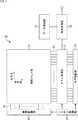
本適用例に係るCMOSイメージセンサ10は、図示せぬ半導体基板(チップ)上に形成された画素アレイ部11と、当該画素アレイ部11と同じ半導体基板上に集積された周辺回路部とを有する構成となっている。周辺回路部は、例えば、垂直駆動部12、カラム処理部13、水平駆動部14およびシステム制御部15から構成されている。 A
CMOSイメージセンサ10はさらに、信号処理部18およびデータ格納部19を備えている。信号処理部18およびデータ格納部19については、CMOSイメージセンサ10と同じ基板上に搭載しても構わないし、CMOSイメージセンサ10とは別の基板上に配置するようにしても構わない。また、信号処理部18およびデータ格納部19の各処理については、CMOSイメージセンサ10とは別の基板に設けられる外部信号処理部、例えば、DSP(Digital Signal Processor)回路やソフトウェアによる処理でも構わない。 The
画素アレイ部11は、受光した光量に応じた電荷を生成しかつ蓄積する光電変換部を有する単位画素(以下、単に「画素」と記述する場合もある)が行方向および列方向に、すなわち、行列状に2次元配置された構成となっている。ここで、行方向とは画素行の画素の配列方向(すなわち、水平方向)をいい、列方向とは画素列の画素の配列方向(すなわち、垂直方向)をいう。単位画素の具体的な回路構成や画素構造の詳細については後述する。 The
画素アレイ部11において、行列状の画素配列に対して、画素行毎に画素駆動線16が行方向に沿って配線され、画素列毎に垂直信号線17が列方向に沿って配線されている。画素駆動線16は、画素から信号を読み出す際の駆動を行うための駆動信号を伝送する。図1では、画素駆動線16について1本の配線として示しているが、1本に限られるものではない。画素駆動線16の一端は、垂直駆動部12の各行に対応した出力端に接続されている。 In the
垂直駆動部12は、シフトレジスタやアドレスデコーダなどによって構成され、画素アレイ部11の各画素を全画素同時あるいは行単位等で駆動する。すなわち、垂直駆動部12は、当該垂直駆動部12を制御するシステム制御部15と共に、画素アレイ部11の各画素の動作を制御する駆動部を構成している。この垂直駆動部12はその具体的な構成については図示を省略するが、一般的に、読出し走査系と掃き出し走査系の2つの走査系を有する構成となっている。 The
読出し走査系は、単位画素から信号を読み出すために、画素アレイ部11の単位画素を行単位で順に選択走査する。単位画素から読み出される信号はアナログ信号である。掃き出し走査系は、読出し走査系によって読出し走査が行われる読出し行に対して、その読出し走査よりも露光時間分だけ先行して掃き出し走査を行う。 The readout scanning system selectively scans the unit pixels of the
この掃き出し走査系による掃き出し走査により、読出し行の単位画素の光電変換部から不要な電荷が掃き出されることによって当該光電変換部がリセットされる。そして、この掃き出し走査系による不要電荷の掃き出す(リセットする)ことにより、所謂電子シャッタ動作が行われる。ここで、電子シャッタ動作とは、光電変換部の電荷を捨てて、新たに露光を開始する(電荷の蓄積を開始する)動作のことをいう。 By the sweep scanning by the sweep scanning system, unnecessary charges are swept out from the photoelectric conversion unit of the unit pixel in the readout row, thereby resetting the photoelectric conversion unit. A so-called electronic shutter operation is performed by sweeping out (resetting) unnecessary charges by the sweep-out scanning system. Here, the electronic shutter operation refers to an operation in which the electric charge of the photoelectric conversion unit is discarded and exposure is newly started (charge accumulation is started).
読出し走査系による読出し動作によって読み出される信号は、その直前の読出し動作または電子シャッタ動作以降に受光した光量に対応するものである。そして、直前の読出し動作による読出しタイミングまたは電子シャッタ動作による掃き出しタイミングから、今回の読出し動作による読出しタイミングまでの期間が、単位画素における電荷の露光期間となる。 The signal read by the reading operation by the reading scanning system corresponds to the amount of light received after the immediately preceding reading operation or electronic shutter operation. The period from the read timing by the previous read operation or the sweep timing by the electronic shutter operation to the read timing by the current read operation is the charge exposure period in the unit pixel.
垂直駆動部12によって選択走査された画素行の各単位画素から出力される信号は、画素列毎に垂直信号線17の各々を通してカラム処理部13に入力される。カラム処理部13は、画素アレイ部11の画素列毎に、選択行の各画素から垂直信号線17を通して出力される信号に対して所定の信号処理を行うと共に、信号処理後の画素信号を一時的に保持する。 A signal output from each unit pixel of the pixel row selectively scanned by the
具体的には、カラム処理部13は、信号処理として少なくとも、ノイズ除去処理、例えばCDS(Correlated Double Sampling;相関二重サンプリング)処理や、DDS(Double Data Sampling)処理を行う。例えば、CDS処理により、リセットノイズや画素内の増幅トランジスタの閾値ばらつき等の画素固有の固定パターンノイズが除去される。カラム処理部13にノイズ除去処理以外に、例えば、AD(アナログ−デジタル)変換機能を持たせ、アナログの画素信号をデジタル信号に変換して出力することも可能である。 Specifically, the
水平駆動部14は、シフトレジスタやアドレスデコーダなどによって構成され、カラム処理部13の画素列に対応する単位回路を順番に選択する。この水平駆動部14による選択走査により、カラム処理部13において単位回路毎に信号処理された画素信号が順番に出力される。 The
システム制御部15は、各種のタイミング信号を生成するタイミングジェネレータなどによって構成され、当該タイミングジェネレータで生成された各種のタイミングを基に、垂直駆動部12、カラム処理部13、および、水平駆動部14などの駆動制御を行う。 The
信号処理部18は、少なくとも演算処理機能を有し、カラム処理部13から出力される画素信号に対して演算処理等の種々の信号処理を行う。また、信号処理部18は、後述する本技術のゲイン乗算処理を行うためのアンプを備える。 The
データ格納部19は、信号処理部18での信号処理に当たって、その処理に必要なデータを一時的に格納する。 The
{他のシステム構成}
本技術が適用されるCMOSイメージセンサ10としては、上述したシステム構成のものに限られるものではない。他のシステム構成として、以下のようなシステム構成のものを挙げることができる。{Other system configuration}
The
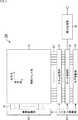
例えば、図2に示すように、データ格納部19をカラム処理部13の後段に配置し、カラム処理部13から出力される画素信号を、データ格納部19を経由して信号処理部18に供給するシステム構成のCMOSイメージセンサ10Aを挙げることができる。 For example, as shown in FIG. 2, the
さらには、図3に示すように、画素アレイ部11の列毎あるいは複数の列毎にAD変換するAD変換機能をカラム処理部13に持たせると共に、当該カラム処理部13に対してデータ格納部19および信号処理部18を並列的に設けるシステム構成のCMOSイメージセンサ10Bを挙げることができる。 Furthermore, as shown in FIG. 3, the
<第1の実施の形態>
次に、図4乃至図10を参照して、本技術の第1の実施の形態について説明する。<First Embodiment>
Next, a first embodiment of the present technology will be described with reference to FIGS. 4 to 10.
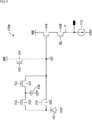
{単位画素100Aの回路構成}
図4は、図1乃至図3の画素アレイ部11に配置される単位画素100Aの構成例を示す回路図あり、図5は、単位画素100Aの構成例を示す平面レイアウト図である。また、図5では、一例として、単位画素100Aが、いわゆる裏面照射型の撮像装置である場合の構造を示している。{Circuit configuration of
FIG. 4 is a circuit diagram illustrating a configuration example of the
単位画素100Aは、PD(フォトダイオード)101、第1転送トランジスタ102、第2転送トランジスタ103、第3転送トランジスタ104、メモリ部105、リセットトランジスタ106、FD部107、増幅トランジスタ108、および選択トランジスタ109を備えて構成される。 The
PD101は、入射した光を光電変換により電荷に変換して蓄積する光電変換部であり、アノード端子が接地されていると共に、カソード端子が第1転送トランジスタ102と第2転送トランジスタ103にそれぞれ接続されている。 The
第1転送トランジスタ102は、垂直駆動部12(図1)から供給される転送信号TG1に従って駆動し、第1転送トランジスタ102がオンになると、PD101に蓄積されている電荷がメモリ部105に転送される。メモリ部105は、電荷を一時的に保持する電荷保持部として機能する。 The
第2転送トランジスタ103は、垂直駆動部12(図1)から供給される転送信号TG2に従って駆動し、第2転送トランジスタ103がオンになると、PD101に蓄積されている電荷がFD部107に転送される。 The
第3転送トランジスタ104は、垂直駆動部12(図1)から供給される転送信号TG3に従って駆動し、第3転送トランジスタ104がオンになると、メモリ部105に蓄積されている電荷がFD部107に転送される。 The
FD部107は、増幅トランジスタ108のゲート電極に接続された所定の蓄積容量を有する浮遊拡散領域であり、PD101から直接的および間接的(メモリ部105を介して)転送される電荷を蓄積する。 The
増幅トランジスタ108は、FD部107に蓄積されている電荷に応じたレベル(即ち、FD部107の電圧)の画素信号を、選択トランジスタ109を介して垂直信号線17に出力する。すなわち、FD部107が増幅トランジスタ108のゲート電極に接続される構成により、FD部107および増幅トランジスタ108は、PD101において発生した電荷を、その電荷に応じたレベルの画素信号に変換する変換部(電荷電圧変換部)として機能する。 The
選択トランジスタ109は、垂直駆動部12(図1)から供給される選択信号SELに従って駆動し、選択トランジスタ109がオンになると、増幅トランジスタ108から出力される画素信号が垂直信号線17に出力可能な状態となる。垂直信号線17には、ソースフォロワ回路を構成する定電流源110が接続されている。 The
リセットトランジスタ106は、垂直駆動部12から供給されるリセット信号RSTに従って駆動し、リセットトランジスタ106がオンになると、FD部107に蓄積されている電荷が電源配線Vddに排出されて、FD部107がリセットされる。 The
なお、以下、各駆動信号がアクティブ状態になることを、各駆動信号がオンするともいい、各駆動信号が非アクティブ状態になることを、各駆動信号がオフするともいう。また、以下、各ゲート部または各トランジスタが導通状態になることを、各ゲート部または各トランジスタがオンするともいい、各ゲート部または各トランジスタが非導通状態になることを、各ゲート部または各トランジスタがオフするともいう。 In the following description, each drive signal is in an active state, each drive signal is turned on, and each drive signal is in an inactive state, each drive signal is also turned off. In addition, hereinafter, each gate portion or each transistor is turned on, each gate portion or each transistor is also turned on, and each gate portion or each transistor is turned off, each gate portion or each transistor is turned on. It is also said that the transistor is turned off.
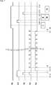
裏面照射型の撮像装置において、PD101が形成されたシリコン基板は、フォトダイオードへの光の入射面となる第1の面と、第1の面に対向する第2の面と、を備える。図5は、単位画素100Aに関わる、シリコン基板の第2の面における平面レイアウト図であって、単位画素100Aに備わる活性領域、光電変換部、画素トランジスタ、電荷蓄積部、およびこれらの間を接続する配線の、平面レイアウト図である。 In the back-illuminated imaging device, the silicon substrate on which the
図5において、PD101、第1転送トランジスタ102、第2転送トランジスタ103、第3転送トランジスタ104、メモリ部105、リセットトランジスタ106、FD部107、および電源VDDへの接続部が、連続した第1の活性領域上に形成されている。 In FIG. 5, the
第1の活性領域とは別に、増幅トランジスタ108、および選択トランジスタ109、電源VDDへの接続部および垂直信号線17への接続部が、連続した第2の活性領域上に形成されている。 Apart from the first active region, an
図5において、FD部107と、増幅トランジスタ108のゲート電極との間は、ゲート電極よりも上層に配置された配線によって接続されている。 In FIG. 5, the
なお、第1転送トランジスタ102は、例えばゲート部に第1の電圧(例えば負電圧)を印加した際には、ゲート電極下方のチャネル領域に、オーバーフローパスが形成されるようにチャネル領域の不純物濃度が設定されているように構成することも可能である。 The
このように構成されている場合、PD101に強い光が入射して、これによって発生した電荷がPD101の飽和蓄積量を超えた場合には、PD101から溢れた電荷が、このオーバーフローパスを経由してメモリ部105へと転送される構成とすることができる。 In such a configuration, when strong light is incident on the
図6に単位画素100Aの断面図を示す。図6の上部には、参考のため、図5に示した単位画素100Aの平面図を示し、下部に単位画素100Aの断面図を示す。図6の上部に示した平面図に示した直線A〜Bの断面図が、図6の上図の平面に対応して、下図に描かれており、同じ部位には同じ番号が付してある。 FIG. 6 shows a cross-sectional view of the unit pixel 100A. 6 is a plan view of the
図6に示すように、FD部107とPD101との間に、第2転送トランジスタ103が形成されている。また、PD101とメモリ部105との間に、第1転送トランジスタ102が形成されている。また、メモリ部105とFD部107との間に、第3転送トランジスタ104が形成されている。そして、FD部107は、増幅トランジスタ108に配線により接続されている。 As shown in FIG. 6, the
このように、本技術を適用した単位画素100Aは、PD101で蓄積された電荷をメモリ部105に一旦蓄積してから、FD部107に転送するための第1転送トランジスタ102と第3転送トランジスタ104を備える。また、単位画素100Aは、PD101で蓄積された電荷をFD部107に転送するための第2転送トランジスタ103を備える。 As described above, the
このように、第1の実施の形態における単位画素100Aは、3個の転送トランジスタとメモリを備え、PD101からFD部107に直接的に電荷を転送する転送トランジスタと、メモリを介して間接的に電荷を転送する転送トランジスタとが備えられている。 As described above, the
{単位画素の動作}
図7を参照して、このような構成を有する単位画素100Aの動作について説明する。{Operation of unit pixel}
The operation of the
図7は、第1の実施の形態における単位画素100Aに備わる選択トランジスタ109を駆動する選択信号SEL、リセットトランジスタ106を駆動するリセット信号RST、第3転送トランジスタ104を駆動する転送信号TG3、第2転送トランジスタ103を駆動する転送信号TG2、および第1転送トランジスタ102を駆動する転送信号TG1のタイミングチャートを示す。 FIG. 7 illustrates a selection signal SEL for driving the
まず、リセットトランジスタ106のゲート部がオンにされ、その期間中に第2転送トランジスタ103、第3転送トランジスタ104のそれぞれのゲート部もオンにされる。 First, the gate portion of the
図7に示したタイミングチャートを参照するに、時刻t1にリセット信号RSTがオンにされることで、リセットトランジスタ106が、オンにされる。時刻t1後の時刻t2において、転送信号TG2と転送信号TG3が、それぞれオンにされることで、第2転送トランジスタ103、第3転送トランジスタ104が、それぞれオンにされる。これらの動作により、単位画素100Aに備わるPD101、メモリ部105、およびFD部107がそれぞれリセットされる。 Referring to the timing chart shown in FIG. 7, when the reset signal RST is turned on at time t1, the
PD101、メモリ部105、およびFD部107がそれぞれリセットされた後、第2転送トランジスタ103、第3転送トランジスタ104、およびリセットトランジスタ106のそれぞれのゲート部がオフにされる。 After the
図7に示したタイミングチャートを参照するに、時刻t3に、転送信号TG2と転送信号TG3が、それぞれオフにされることで、第2転送トランジスタ103、第3転送トランジスタ104が、それぞれオフにされる。時刻t3後の時刻t4において、リセット信号RSTがオフにされることで、リセットトランジスタ106が、オフにされる。 Referring to the timing chart shown in FIG. 7, at time t3, the transfer signal TG2 and the transfer signal TG3 are turned off, so that the
リセット動作が行われた後、PD101において光電変換の結果発生した電荷が蓄積される蓄積期間が開始される。この蓄積期間においては、第2転送トランジスタ103と第1転送トランジスタ102が、交互にオン、オフされる。 After the reset operation is performed, an accumulation period in which charges generated as a result of photoelectric conversion in the
すなわち、時刻t4において、転送信号TG1がオンにされることで、第1転送トランジスタ102がオンにされ、時刻t5において、転送信号TG1がオフにされることで、第1転送トランジスタ102がオフにされる。 That is, at time t4, the transfer signal TG1 is turned on to turn on the
また時刻t5において、転送信号TG2がオンにされることで、第2転送トランジスタ103がオンにされ、時刻t6において、転送信号TG2がオフにされることで、第2転送トランジスタ103がオフにされる。 At time t5, the transfer signal TG2 is turned on to turn on the
第1転送トランジスタ102がオンにされることで、PD101に蓄積されている信号電荷が、メモリ部105に転送される。また、第2転送トランジスタ103がオンにされることで、PD101に蓄積されている信号電荷が、FD部107に転送される。 When the
このように、PD101において光電変換の結果発生した電荷が蓄積される蓄積期間において、第1転送トランジスタ102と第2転送トランジスタ103が、交互にオンにされることで、PD101で蓄積されている信号電荷が、メモリ部105とFD部107に交互に転送される。 Thus, in the accumulation period in which charges generated as a result of photoelectric conversion in the
第1転送トランジスタ102は、時刻t4から時刻t7の間、オン、オフを繰り返すことで、PD101からメモリ部105に信号電荷を転送する。また、第2転送トランジスタ103は、時刻t5から時刻t8の間、オン、オフを繰り返すことで、PD101からFD部107に信号電荷を転送する。 The
ここで、図8を参照して、図7のタイミングチャートの時刻t4乃至t6における単位画素100Aの動作の詳細について説明する。図8Aは、単位画素100Aの断面構造を示し、図6に示した断面構造を参考のために図示した。図8B,図8C,図8Dは、時刻t4乃至t6それぞれにおける単位画素100Aのポテンシャル図を示している。また図中黒塗りの四角は、その駆動信号がオンされていることを示し、白抜きの四角は、その駆動信号がオフされていることを示している。 Here, with reference to FIG. 8, the details of the operation of the
図8Bは、例えば、時刻t4におけるポテンシャルの状態を表し、PD101に電荷が蓄積される前の状態であり、メモリ部105およびFD部107がリセットされた状態を示している。図8Bに示すように、第1転送トランジスタ102は、PD101とメモリ部105との間に設けられ、メモリ部105のポテンシャルは、PD101のポテンシャルよりも深くされている。 FIG. 8B shows, for example, a potential state at time t4, which is a state before charge is accumulated in the
メモリ部105のポテンシャルは、PD101のポテンシャルよりも深くされていることで、第1転送トランジスタ102の駆動により、PD101からメモリ部105に信号電荷を転送できる。PD101からメモリ部101へ電荷を転送し、転送した電荷をメモリ部105に蓄積すると、蓄積した電荷の量に応じてメモリ部105のポテンシャルが、図8Bに示したメモリ部105のポテンシャルよりも浅くなる。電荷を蓄積することでメモリ部105のポテンシャルが浅くなり、メモリ部105のポテンシャルが図8Bに示したPD101のポテンシャルと等しくなるまで、メモリ部105は電荷を蓄積できる。 Since the potential of the
図8Bに示したような状態のとき、PD101において電荷の蓄積が開始され、第1転送トランジスタ102がオンにされると、図8Cに示すように、PD101の信号電荷は、メモリ部105に転送される。その後、第1転送トランジスタ102がオフにされると、PD101とメモリ部105の間にポテンシャル障壁が形成され、PD101からメモリ部105への信号電荷の転送が停止される。 In the state shown in FIG. 8B, when charge accumulation is started in the
時刻t5において、第1転送トランジスタ102がオフにされる一方で、第2転送トランジスタ103がオンにされると、PD101からFD部107に信号電荷が転送される。 At time t5, when the
このように、メモリ部105への電荷の転送と、FD部107への電荷の転送が行われる。 In this manner, charge transfer to the
このような動作が露光期間に交互に繰り返されることで、露光期間にPD101で光電変換された信号電荷のうち、第1転送トランジスタ102がオンにされていた期間(第1期間とする)内に発生した信号電荷は、メモリ部105に転送され、蓄積/保持される。また、露光期間にPD101で光電変換された信号電荷のうち、第2転送トランジスタ103がオンにされていた期間(第2期間とする)内に発生した信号電荷は、FD部107に転送され、蓄積/保持される。 Such an operation is alternately repeated during the exposure period, so that the signal charge photoelectrically converted by the
ここで、第1期間の方が、第2期間よりも長い期間であるとする。換言すれば、PD101から信号電荷をメモリ部105に転送する期間の方が、FD部107に転送する期間よりも長い期間であるとする。この第1期間、第2期間は、露光時間に長さに相当するため、第1期間内に蓄積された信号電荷は、長い露光時間で蓄積された信号電荷に相当し、第2期間内に蓄積された信号電荷は、短い露光時間で蓄積された信号電荷に相当する。 Here, it is assumed that the first period is longer than the second period. In other words, it is assumed that the period during which signal charges are transferred from the
図7において時刻t4から時刻t8までの間、単位画素100Aは、PD101へ入射した光によって発生した電荷を、信号電荷として蓄積している。より具体的には、単位画素100Aは、時刻t4から時刻t8までの間、第1転送トランジスタ102と第2転送トランジスタ103を交互にオンまたはオフすることにより、PD101へ入射した光によって発生した電荷を、メモリ部105またはFD部107のどちらかに、信号電荷として蓄積している。 In FIG. 7, from time t4 to time t8, the
メモリ部105に電荷が蓄積される第1期間を、FD部107に電荷が蓄積される第2期間よりも長いと仮定すると、時刻t4から時刻t8までの間に、メモリ部105に蓄積/保持される信号電荷の量は、FD部107に蓄積/保持される信号電荷の量よりも多い。 Assuming that the first period in which charges are accumulated in the
このため、メモリ部105に電荷が蓄積される第1期間を、FD部107に電荷が蓄積される第2期間よりも長いと仮定すると、PD101へ入射した光によって発生した電荷を、より多く蓄積/保持しているメモリ部105から得られる信号は、PD101へ入射した光に対する感度が高い信号と呼ぶことができる。 Therefore, assuming that the first period in which charges are accumulated in the
一方、PD101へ入射した光によって発生した電荷を、これよりも少なく蓄積/保持しているFD部107から得られる信号は、PD101へ入射した光に対する感度が低い信号と呼ぶことができる。 On the other hand, a signal obtained from the
以後、第1転送トランジスタ102がオンにされ、メモリ部105に蓄積/保持される信号電荷(第1期間で蓄積/保持される信号電荷)の方を、高感度データ信号(以下、高感度データ信号SHと記述する)と呼ぶ。また、第2転送トランジスタ103がオンにされ、FD部107に蓄積/保持される信号電荷(第2期間で蓄積/保持される信号電荷)の方を、低感度データ信号(以下、低感度データ信号SLと記述する)と呼ぶ。 Thereafter, the
このように、本技術によれば、高感度データ信号SHと低感度データ信号SLを得ることができ、高感度データ信号SHと低感度データ信号SLを用いた後述するような処理により、ダイナミックレジが拡大された画像を撮像することが可能となる。 As described above, according to the present technology, the high sensitivity data signal SH and the low sensitivity data signal SL can be obtained, and the dynamic registration is performed by the process described later using the high sensitivity data signal SH and the low sensitivity data signal SL. It is possible to capture an image in which is enlarged.
上記したような蓄積期間が終了後、読み出し期間へと移行する。蓄積期間内では、上記したような処理、すなわち、リセットからメモリ部105またはFD部107への転送までの処理を、画素アレイ部11内の全画素同時に行うことで、全画素で蓄積時間が同一のグローバルシャッターを実現することができる。 After the accumulation period as described above ends, the period shifts to the reading period. Within the accumulation period, the processing as described above, that is, the processing from reset to transfer to the
次に読み出し期間内の動作について説明する。時刻t9において、選択信号SELがオンにされることで、選択トランジスタ109がオンの状態にされる。選択トランジスタ109がオンにされることで、増幅トランジスタ108を介して、FD部107に蓄積されている電荷に応じたレベル(即ち、FD部107の電圧)の画素信号が垂直信号線17に出力される。 Next, an operation within the reading period will be described. At time t9, the selection signal SEL is turned on, so that the
蓄積期間直後にFD部107から読み出される画素信号は、PD101から第2転送トランジスタ103によりFD部107に転送された信号電荷に対応する信号、換言すれば、第2期間内に蓄積された信号電荷に対応する信号である。すなわち、低感度データ信号SLである。 The pixel signal read from the
低感度データ信号SLの読み出し後、高感度データ信号SHの読み出しが行われる。まず時刻t10において、リセット信号RSTがオンにされることで、リセットトランジスタ106がオンの状態にされる。その後、時刻t11において、リセット信号RSTがオフにされることで、リセットトランジスタ106がオフの状態にされる。リセットトランジスタ106がオンおよびオフにされることで、FD部107がリセットされる。 After the low sensitivity data signal SL is read, the high sensitivity data signal SH is read. First, at time t10, the reset signal RST is turned on, so that the
時刻t11後、FD部107のリセット後の信号(FDレベル)が、選択トランジスタ109を介して垂直信号線17に出力される。この信号を、低感度リセット信号NLと記述する。この低感度リセット信号NLは、次に読み出されるメモリ部105に蓄積されていた信号に対するP相(高感度リセット信号NHと記述する)に該当する。 After time t11, a signal (FD level) after reset of the
時刻t12において、転送信号TG3がオンにされることで、第3転送トランジスタ104がオンの状態とされる。第3転送トランジスタ104がオンの状態となることで、メモリ部105に蓄積されていた信号電荷が、FD部107に転送される。時刻t13において、転送信号TG3がオフにされることで、第3転送トランジスタ104がオフの状態とされる。 At time t12, the transfer signal TG3 is turned on, so that the
このとき、選択トランジスタ109は、オンの状態とされているため、増幅トランジスタ108を介して、FD部107に蓄積されている電荷に応じたレベル(即ち、FD部107の電圧)の画素信号が垂直信号線17に出力される。 At this time, since the
このときFD部107から読み出される画素信号は、PD101から第1転送トランジスタ102によりメモリ部105に一旦転送され、第3転送トランジスタ104によりメモリ部105からFD部107に転送された信号電荷に対応する信号、換言すれば、第1期間内に蓄積された信号電荷に対応する信号である。すなわち、高感度データ信号SHである。 At this time, the pixel signal read from the
このように、低感度データ信号SLの読み出し後に引き続き、高感度データ信号SHの読み出しが行われる。 As described above, the high sensitivity data signal SH is read after the low sensitivity data signal SL is read.
低感度データ信号SLは、上記したように、第2転送トランジスタ103がオンにされていた第2期間内に発生した信号電荷である。この第2期間は、第2転送トランジスタ103が1回にオンされている時間(時間T2とする)と、蓄積期間内での第2転送トランジスタ103がオンにされる回数に依存する期間である。 As described above, the low sensitivity data signal SL is a signal charge generated in the second period in which the
また、高感度データ信号SHは、上記したように、第1転送トランジスタ102がオンにされていた第1期間内に発生した信号電荷である。この第1期間は、第1転送トランジスタ102が1回にオンされている時間(時間T1とする)と、蓄積期間内での第1転送トランジスタ102がオンにされる回数に依存する期間である。 Further, as described above, the high-sensitivity data signal SH is a signal charge generated during the first period in which the
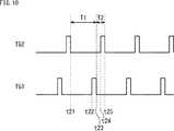
図9、図10を参照し、時間T1と時間T2について説明を加える。図9は、第1転送トランジスタ102と第2転送トランジスタ103を、それぞれ時間T1、時間T2のオン時間で交互に駆動している状態を表している。図9における時間T1は、図7における時刻t4から時刻t5までの時間に相当し、時間T2は、時刻t5から時刻t6の時間に相当する。 With reference to FIG. 9 and FIG. 10, the time T1 and the time T2 will be described. FIG. 9 shows a state in which the
このような動作により、
全露光時間×時間T1/(時間T1+時間T2)
で光電変換された信号電荷のみを、第1転送トランジスタ102を介して、メモリ部105に転送することができる。また
全露光時間×時間T2/(時間T1+時間T2)
で光電変換された信号電荷のみを、第2転送トランジスタ103を介して、FD部107に転送することができる。With this behavior,
Total exposure time x time T1 / (time T1 + time T2)
Only the signal charge photoelectrically converted in step S <b> 1 can be transferred to the
Only the signal charge photoelectrically converted in step S <b> 1 can be transferred to the
すなわち、実効的に、感度を、T1:T2の比で変換した信号データを、それぞれメモリ部105とFD部107に保持させることになる。 That is, the signal data obtained by converting the sensitivity with the ratio of T1: T2 is effectively held in the
このことは、時間T1と時間T2を変えることで、任意の感度調整を行うことができることも意味する。すなわち、時間T1と時間T2を変えることで、換言すれば、転送信号TG1のオン、オフの時間と、転送信号TG2のオン、オフの時間を調整することで、感度を調整することができる。 This also means that arbitrary sensitivity adjustment can be performed by changing the time T1 and the time T2. That is, by changing the time T1 and the time T2, in other words, the sensitivity can be adjusted by adjusting the on / off time of the transfer signal TG1 and the on / off time of the transfer signal TG2.
また、時間T1と時間T2(第1期間と第2期間)を設けて撮影を行うため、例えばLED(Light Emitting Diode)フリッカなどにより影響を受けづらい撮影を行うことができる。LED照明は、常時点灯ではなく、所定の周期で点滅している。このため、短シャッタで撮影を行うとき、露光タイミングとLEDの点滅の消灯のタイミングが重なると、LEDが消えた画が撮影されてしまう。 In addition, since shooting is performed with time T1 and time T2 (first period and second period), it is possible to perform shooting that is not easily affected by, for example, LED (Light Emitting Diode) flicker. The LED illumination is not constantly lit but blinks at a predetermined cycle. For this reason, when shooting with a short shutter, if the exposure timing overlaps with the blinking and extinguishing timing of the LED, an image with the LED turned off is shot.
例えば、1回の短シャッタでもシャッタ時間で感度の低下を実現できるが、1回の短シャッタが、上記したように、LEDの点滅の消灯のタイミングが重なると、画が撮像できない可能性がある。しかしながら、本技術によれば、時間T1と時間T2という異なる時間を用いて撮影を行うため、仮に、時間T1と時間T2のうちの一方の時間が、LEDの点滅の消灯のタイミングと重なってしまっても、他方の時間で撮影を行うことができる。 For example, the sensitivity can be reduced by the shutter time even with one short shutter, but if the timing of the blinking of the LED blinking overlaps as described above, there is a possibility that the image cannot be captured. . However, according to the present technology, since shooting is performed using different times of the time T1 and the time T2, one of the time T1 and the time T2 is overlapped with the timing of turning off and blinking the LED. However, shooting can be performed at the other time.
よって、LEDフリッカなどにより、画が撮像できないようなことを防ぐことが可能となる。 Therefore, it is possible to prevent an image from being captured due to LED flicker or the like.
図9では、第1転送トランジスタ102と第2転送トランジスタ103は、排他的に動作させる例を示したが、完全転送ができるパルス幅が取れれば、図10のような動作も可能となる。図10に示したように、一方のパルスを立ち下げてから他方のパルスを立ち下げるまでが、時間T1、時間T2となればよい。 FIG. 9 shows an example in which the
例えば、時刻t21において、転送信号TG2がオフにされた後、時刻t22において、転送信号TG1がオンにされ、その転送信号TG1が、時刻t23でオフにされる。この時刻t21から時刻t23までが時間T1とされる。この場合、時刻t21から時刻t23、すなわち時間T1の間、PD101で蓄積された電荷が、時刻t22から時刻t23の間に、第1転送トランジスタ102がオンされ、PD101からメモリ部105に転送される。 For example, after the transfer signal TG2 is turned off at time t21, the transfer signal TG1 is turned on at time t22, and the transfer signal TG1 is turned off at time t23. The period from time t21 to time t23 is time T1. In this case, the charge accumulated in the
時刻t23の後の時刻t24において、転送信号TG2がオンにされ、その転送信号TG2が、時刻t25でオフにされる。この時刻t23から時刻t25までが時間T2とされる。この場合、時刻t23から時刻t25、すなわち時間T2の間、PD101で蓄積された電荷が、時刻t24から時刻t25の間に、第2転送トランジスタ103がオンされ、PD101からFD部107に転送される。 At time t24 after time t23, the transfer signal TG2 is turned on, and the transfer signal TG2 is turned off at time t25. The period from time t23 to time t25 is time T2. In this case, the charge accumulated in the
このような動作でも、上記した場合、例えば、図9を参照して説明した場合と同様に、低感度データ信号SLと高感度データ信号SHを取得することができる。 Even in such an operation, the low sensitivity data signal SL and the high sensitivity data signal SH can be acquired in the above case, for example, as in the case described with reference to FIG.
このようにして読み出された、低感度データ信号SLと高感度データ信号SHを用いることで、ダイナミックレンジを拡大した撮影を行えることについて、図11を参照して説明を加える。 The use of the low-sensitivity data signal SL and the high-sensitivity data signal SH read out in this manner will allow a description to be taken with an expanded dynamic range with reference to FIG.
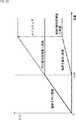
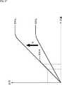
図11は、高感度データ信号SHと低感度データ信号SLの入出力特性を表している。すなわち、時刻t4から時刻t8までの信号電荷蓄積期間にPD101へ入射される光量を横軸にとり、これに対して、PD101での光電変換の結果得られる出力(光電変換の結果蓄積した電荷の量)を縦軸に表している。図11において、PD101での光電変換の結果得られる出力のうち、メモリ部105で保持される高感度データ信号SHは、「MEM保持」と付記した実線でその特性を表した。また、FD部107で保持される低感度データ信号SLは、「FD保持」と付記した実線でその特性を表した。 FIG. 11 shows input / output characteristics of the high sensitivity data signal SH and the low sensitivity data signal SL. That is, the horizontal axis represents the amount of light incident on the
図11において、メモリ部105で保持される高感度データ信号SHの特性は、入射光量が少ない領域においては、グラフの原点を通り、かつ、光量の増加に従って出力が一定の傾きで増加する直線となる。ここで、この直線の傾きを、k1と名付ける。光量の増加に従って蓄積する電荷が増加して、蓄積する電荷がメモリ部105の飽和電荷量に達すると、高感度データ信号SHの特性は、それ以上は光量が増加しても出力が一定となる。すなわち飽和する。ここで、蓄積する電荷がメモリ部105の飽和電荷量に達した時点の光量を、L1と名付ける。また、メモリ部105の飽和電荷量をC1と名付ける。 In FIG. 11, the characteristics of the high-sensitivity data signal SH held in the
図11において、FD部107で保持される低感度データ信号SLの特性は、入射光量が少ない領域においては、グラフの原点を通り、かつ、光量の増加に従って出力が一定の傾きで増加する直線となる。ここで、この直線の傾きを、k2と名付ける。光量の増加に従って蓄積する電荷が増加し、蓄積する電荷がFD部107の飽和電荷量に達すると、低感度データ信号SLの特性は、それ以上は光量が増加しても出力が一定となる。すなわち飽和する。ここで、蓄積する電荷がFD部107の飽和電荷量に達した時点の光量を、L2と名付ける。また、FD部107の飽和電荷量をC2と名付ける。 In FIG. 11, the characteristics of the low-sensitivity data signal SL held by the
ここで、図11に記載の高感度データ信号SHと低感度データ信号SLの特性は、図7と同様に、メモリ部105に電荷が蓄積される第1期間T1が、FD部107に電荷が蓄積される第2期間T2よりも長い、との仮定に基づいたものであり、かつ、FD部107が飽和する電荷量が、メモリ部105が飽和する電荷量よりも大きい、との仮定に基づいたものである。 Here, the characteristics of the high-sensitivity data signal SH and the low-sensitivity data signal SL shown in FIG. 11 are similar to those in FIG. Based on the assumption that it is longer than the accumulated second period T2, and based on the assumption that the amount of charge that
このため、図11に記載の高感度データ信号SHと低感度データ信号SLの特性は、メモリ部105で保持される高感度データ信号SHの傾きk1が、FD部107で保持される低感度データ信号SLの傾きk2よりも大きくなっている。また、低感度データ信号SLが飽和する出力レベル(電荷量)が、高感度データ信号SHが飽和する出力レベル(電荷量)よりも大きくなっている。 Therefore, the characteristics of the high-sensitivity data signal SH and the low-sensitivity data signal SL shown in FIG. 11 are such that the slope k1 of the high-sensitivity data signal SH held in the
さらに、図11に記載の高感度データ信号SHと低感度データ信号SLの特性は、FD部107で保持される低感度データ信号SLの傾きk2が、メモリ部105で保持される高感度データ信号SHの傾きk1よりも小さく、かつ、FD部107が飽和する電荷量C2が、メモリ部105が飽和する電荷量C1よりも大きい、との仮定に基づいたものであるため、低感度データ信号SLが飽和した時点の光量L2は、高感度データ信号SHが飽和した時点の光量L1よりも大きくなっている。 Furthermore, the characteristics of the high-sensitivity data signal SH and the low-sensitivity data signal SL shown in FIG. The low-sensitivity data signal SL is based on the assumption that the charge amount C2 at which the
高感度データ信号SHは低感度データ信号SLよりも低い光量において、出力が飽和する。低感度データ信号SLは高感度データ信号SHの出力が飽和している光量においても、PD101へ入射した光量に応じた信号を出力する。つまり図11に示す入出力特性において、低感度データ信号SLは高感度データ信号SHよりも入力レンジ(PD101へ入射した光量に応じた出力を得ることができる光量の範囲)が広く、これに応じて出力レンジ(PD101へ入射した光量に応じた出力を得られる範囲)も広い。言い換えれば、低感度データ信号SLの特性は高感度データ信号SHの特性よりも、ダイナミックレンジが広い。 The output of the high sensitivity data signal SH is saturated at a light amount lower than that of the low sensitivity data signal SL. The low sensitivity data signal SL outputs a signal corresponding to the amount of light incident on the
そこで、単位画素100Aは、信号処理部18に備わるゲイン乗算処理を行うためのアンプを用いて、低感度データ信号SLへゲインを掛ける処理を行う。より具体的には、図11において、飽和前の高感度データ信号SHの傾きk1と、飽和前の低感度データ信号SLに対してゲインを掛けた所謂ゲインアップ後の傾きが同じになるように、低感度データ信号SLに対してゲインを掛ける。 Therefore, the
図11における破線が、このゲインアップ後の信号を表している。これにより単位画素100Aは、高感度データ信号SHが入射光量に応じた電荷を出力している光量の範囲から、低感度データ信号SLが入射光量に応じた電荷を出力している光量の範囲までとなる、広い範囲に渡って、入力(PD101へ入射した光量)に対して線形な出力(光電変換の結果蓄積した電荷の量)を得ており、ダイナミックレンジの広い特性を備えている。 The broken line in FIG. 11 represents the signal after the gain increase. As a result, the
ここで、図4に記載の単位画素100Aにおいてメモリ部105とFD部107へ交互に電荷を蓄積する動作を行わない形態を、比較例として想定する。すなわち、比較例の単位画素は、図4に記載の単位画素100Aと等価回路上は同じ構成を備え、かつ、単位画素100Aにおけるメモリ部105とFD部107へ交互に電荷を蓄積する動作を行わず、信号電荷蓄積期間にPD101へ入射した光によって発生した電荷は、全てメモリ部105へ転送して蓄積する動作を行うものとする。 Here, a mode in which the operation of alternately accumulating charges in the
図11において、比較例の入出力特性(入射光量に対して、光電変換の結果蓄積した電荷の量)を考える(不図示)。比較例の特性は、入射光量が少ない領域においては、図11に実線で記載した本技術の第1の実施の形態の高感度データ信号SHと同様に、図11のグラフの原点を通り、かつ、光量の増加に従って出力が一定の傾きで増加する直線となる。ここで、この直線の傾きを、k0と名付ける。 In FIG. 11, the input / output characteristics of the comparative example (the amount of charge accumulated as a result of photoelectric conversion with respect to the amount of incident light) are considered (not shown). In the region where the amount of incident light is small, the characteristic of the comparative example passes through the origin of the graph of FIG. 11 as in the high-sensitivity data signal SH of the first embodiment of the present technology described by the solid line in FIG. As the light quantity increases, the output becomes a straight line increasing at a constant slope. Here, the slope of this straight line is named k0.
さらに比較例の特性は、光量の増加に従って蓄積する電荷が増加し、蓄積する電荷がメモリ部105の飽和電荷量に達すると、それ以上は光量が増加しても出力が一定となる。ここで、蓄積する電荷がメモリ部105の飽和電荷量に達した時点の光量を、L0と名付ける。 Furthermore, the characteristic of the comparative example is that the accumulated charge increases as the amount of light increases, and when the accumulated charge reaches the saturation charge amount of the
上に述べた比較例の特性と、図11に記載の本技術の第1の実施の形態の特性を比較する。 The characteristics of the comparative example described above are compared with the characteristics of the first embodiment of the present technology illustrated in FIG.
比較例は、信号電荷蓄積期間にPD101で発生した電荷を、全てメモリ部105へ転送して蓄積する。 In the comparative example, all the charges generated in the
一方、図11に記載の本技術の第1の実施の形態は、信号電荷蓄積期間にPD101で発生した電荷の総量のうち、T1/(T1+T2)の割合に相当する量だけを、メモリ部105へ転送して蓄積する。その特性は、高感度データ信号SHの特性として、図11において「MEM保持」と付記した実線で表されている。高感度データ信号SHの特性の直線部分の傾きk1は、k0のT1/(T1+T2)倍に抑えられている。また、高感度データ信号SHの特性が飽和する時点での光量L1は、L0の(T1+T2)/T1倍に増加する。 On the other hand, in the first embodiment of the present technology shown in FIG. 11, only the amount corresponding to the ratio of T1 / (T1 + T2) out of the total amount of charges generated in the
さらに、図11に記載の本技術の第1の実施の形態は、信号電荷蓄積期間にPD101で発生した電荷の総量のうち、T2/(T1+T2)の割合に相当する量だけを、FD部107へ転送して蓄積する。その特性は、低感度データ信号SLの特性として、図11において「FD保持」と付記した実線で表されている。低感度データ信号SLの特性の直線部分の傾きk2は、k0のT2/(T1+T2)倍に抑えられている。また、低感度データ信号SLの特性が飽和する時点での光量L2は、L0の(C2/C1)×(T1+T2)/T2倍に増加する。 Furthermore, in the first embodiment of the present technology illustrated in FIG. 11, only the amount corresponding to the ratio of T2 / (T1 + T2) out of the total amount of charges generated in the
このため、飽和前の高感度データ信号SHの傾きk1と、飽和前の低感度データ信号SLに対してゲインを掛けた所謂ゲインアップ後の傾きが同じになるように、低感度データ信号SLに対してゲインを掛ける処理を行った本技術の第1の実施の形態の特性(図11の破線)は、入力レンジ(PD101へ入射した光量に応じた出力を得ることができる光量の範囲)が比較例の(C2/C1)×(T1+T2)/T2倍に拡大している。また、出力レンジ(PD101へ入射した光量に応じた出力を得られる範囲)は、比較例との入力レンジの比(C2/C1)×(T1+T2)/T2に、比較例の傾きk0と高感度データ信号SHの傾きk1の比T1/(T1+T2)を乗じた結果である、(C2/C1)×(T1/T2)倍となる。 For this reason, the low-sensitivity data signal SL is set so that the slope k1 of the high-sensitivity data signal SH before saturation and the so-called slope after gain increase obtained by multiplying the low-sensitivity data signal SL before saturation by the gain are the same. The characteristic (dashed line in FIG. 11) of the first embodiment of the present technology in which the process of multiplying the gain is performed on the input range (the light amount range in which an output corresponding to the light amount incident on the
なお、図11に記載の本技術の第1の実施の形態の特性は、T1>T2かつC2>C1を前提としている。 The characteristics of the first embodiment of the present technology illustrated in FIG. 11 are premised on T1> T2 and C2> C1.
結果として、本技術の第1の実施の形態の単位画素100Aは、比較例に対して、入力レンジが(C2/C1)×(T1+T2)/T2倍、出力レンジが(C2/C1)×(T1/T2)倍に拡大した、ダイナミックレンジの広いものとなっている。 As a result, the
図11に記載の本技術の第1の実施の形態の特性は、T1>T2かつC2>C1を前提としたが、仮に、C2≦C1となる条件下であっても、(C2/C1)×(T1/T2)>1となるように、T1とT2を設定すれば、本技術の第1の実施の形態の単位画素100Aは、比較例よりもダイナミックレンジの広い特性を備える。同様に、T1≦T2となる条件下であっても、(C2/C1)×(T1/T2)>1となるように、C1とC2を設定すれば、本技術の第1の実施の形態の単位画素100Aは、比較例よりもダイナミックレンジの広い特性を備える。 The characteristics of the first embodiment of the present technology illustrated in FIG. 11 are based on the premise that T1> T2 and C2> C1, but even if the condition of C2 ≦ C1 is satisfied, (C2 / C1) If T1 and T2 are set so that x (T1 / T2)> 1, the
なお、本技術の第1の実施の形態の画素100Aは、その出力として、信号電荷の蓄積期間中にPD101へ入射した光量がL1以下の場合は、低感度データ信号SLへゲインを掛けたゲインアップ後の低感度データ信号SLを出力するよりも、高感度データ信号SHを出力するほうが好ましい。これは、メモリ部105で保持される高感度データ信号SHと、FD部107で保持される低感度データ信号SLのノイズレベルが同等であるならば、これにゲインを掛けた低感度データ信号SLのノイズレベルよりも、ゲインを掛けない高感度データ信号SHのほうが、ノイズが少なく、S/N比(Signal Noise比)が良好なためである。 Note that the output of the
さらに、例えば、メモリ部105の構造として、特開2011―199816の図4(A)に記載の埋め込み型MOSキャパシタを用い、FD部107の構造として、自由電子が多数存在する縮退した半導体領域を一部に含むPN接合容量を用いる場合には、高感度データ信号SHのノイズレベルが、ゲインを掛ける前の低感度データ信号SLのノイズレベルよりも小さくなる可能性が高い。このような場合には、信号電荷の蓄積期間中にPD101へ入射した光量がL1以下の場合に高感度データ信号SHを出力する利点が、さらに大きくなる。 Further, for example, the embedded MOS capacitor described in FIG. 4A of Japanese Patent Application Laid-Open No. 2011-199816 is used as the structure of the
<第2の実施の形態>
次に本技術を適用した第2の実施の形態について説明する。図12は、第2の実施の形態における単位画素100(以下、第2の実施の形態においては、単位画素100Bと記述する)の平面レイアウトを示す図であり、図13は、断面構造を示す図である。<Second Embodiment>
Next, a second embodiment to which the present technology is applied will be described. FIG. 12 is a diagram showing a planar layout of a unit pixel 100 (hereinafter referred to as a
図12に示した第2の実施の形態における単位画素100Bは、第1の実施の形態における単位画素100Aと基本的な構成は同一であるため、同一の部分には同一の符号を付し、その説明は適宜省略する。 Since the basic configuration of the
図12に示した第2の実施の形態における単位画素100Bの平面レイアウトと、図3に示した第1の実施の形態における単位画素100Aの平面レイアウトとを比較するに、単位画素100Bは、第1転送トランジスタ102がメモリ部105上にまで形成されている点が、第1の実施の形態における単位画素100Aと異なる。 Compared with the planar layout of the
図13に示した第2の実施の形態における単位画素100Bの断面構造と、図6に示した第1の実施の形態における単位画素100Aの断面構造とを比較するに、単位画素100Bは、PD101とメモリ部105との間だけでなく、第1転送トランジスタ102がメモリ部105上にまで延ばされて形成されている点が、第1の実施の形態における単位画素100Aと異なる。 13 is compared with the cross-sectional structure of the
図12、図13を参照するに、FD部107とPD101との間に、第2転送トランジスタ103が形成されている。この点は、第1の実施の形態における単位画素100Aと同じである。PD101とメモリ部105との間とメモリ部105の上部にまで第1転送トランジスタ102Bが形成されている。この点は、第1の実施の形態における単位画素100Aと異なる。 Referring to FIGS. 12 and 13, the
また、メモリ部105とFD部107との間に、第3転送トランジスタ104が形成され、FD部107は、増幅トランジスタ108に配線により接続されている。この点は、第1の実施の形態における単位画素100Aと同じである。 A
このように、本技術を適用した単位画素100Bは、PD101で蓄積された電荷をメモリ部105に一旦蓄積してから、FD部107に転送するための第1転送トランジスタ102Bと第3転送トランジスタ104を備える。また、単位画素100Bは、PD101で蓄積された電荷をFD部107に転送するための第2転送トランジスタ103を備える。また、第1転送トランジスタ102Bは、メモリ部105上にまで、拡大されて設けられている。 As described above, the
このように、第1転送トランジスタ102Bが、メモリ部105の上部にまで設けられていることで、第1転送トランジスタ102Bがオンにされると、メモリ部105のポテンシャルが一緒に深くなり、メモリ部105のポテンシャルを深くすることが可能となる。このことについて、図14を参照して説明する。 As described above, since the
なお、第2の実施の形態においても、単位画素100Bの回路図は、第1の実施の形態における単位画素100Aの回路図と同じく、図4に示したようになるため、その説明は省略する。また、基本的な動作も、図7に示したタイミングチャートを参照して説明した場合と同様であるため、その説明は省略する。 Also in the second embodiment, the circuit diagram of the
図14は、図8と同じく、図7のタイミングチャートの時刻t4乃至t6における単位画素100Bの動作の詳細について説明するための図である。図14Aは、単位画素100Bの断面構造を示し、図13に示した断面構造を参考のために図示した。 FIG. 14 is a diagram for explaining the details of the operation of the
図14B,図14C,図14Dは、時刻t4乃至t6のそれぞれにおける単位画素100Bのポテンシャル図を示している。また図中黒塗りの四角は、その駆動信号がオンされていることを示し、白抜きの四角は、その駆動信号がオフされていることを示している。 14B, 14C, and 14D show potential diagrams of the
図14Bは、例えば、時刻t4におけるポテンシャルの状態を表し、PD101に電荷が蓄積される前の状態であり、メモリ部105およびFD部107がリセットされた状態を示している。図14Bに示すように、第1転送トランジスタ102Bは、PD101とメモリ部105との間と、メモリ部105上にまで拡大して設けられ、メモリ部105のポテンシャルは、PD101のポテンシャルとほぼ同程度にされている。 FIG. 14B shows a potential state at time t4, for example, a state before charge is accumulated in the
図14Bに示したような状態のとき、PD101において電荷の蓄積が開始され、第1転送トランジスタ102Bがオンにされると、図14Cに示すように、PD101の信号電荷は、メモリ部105に転送される。第1転送トランジスタ102Bがオンにされると、PD101とメモリ部105との間のポテンシャル障壁と、メモリ部105のポテンシャルが、共に深くなり、PD101からメモリ部105へと、信号電荷を転送できる状態となる。 In the state shown in FIG. 14B, when charge accumulation is started in the
このように、第1転送トランジスタ102Bがオンにされると、PD101とメモリ部105との間のポテンシャル障壁と、メモリ部105のポテンシャルが、共に深くなるため、上記したように、メモリ部105のポテンシャルは、PD101のポテンシャルとほぼ同程度に形成することができる。 As described above, when the
第1の実施の形態においては、図8を参照して説明したように、メモリ部105のポテンシャルは、PD101のポテンシャルよりも深くされている必要があったが、第2の実施の形態においては、メモリ部105のポテンシャルは、PD101のポテンシャルとほぼ同程度にすることができる。 In the first embodiment, as described with reference to FIG. 8, the potential of the
なお、第2の実施の形態においても、メモリ部105のポテンシャルは、PD101のポテンシャルよりも深くされているようにしても勿論良い。 In the second embodiment, the potential of the
第1転送トランジスタ102Bがオフにされると、PD101とメモリ部105の間にポテンシャル障壁が形成され、PD101からメモリ部105への信号電荷の転送が停止される。そして時刻t5において、第1転送トランジスタ102Bがオフにされる一方で、第2転送トランジスタ103がオンにされると、PD101からFD部107に信号電荷が転送される。 When the
このように、メモリ部105への電荷の転送と、FD部107への電荷の転送が行われる。 In this manner, charge transfer to the
このような動作が露光期間に交互に繰り返されることで、露光期間にPD101で光電変換された信号電荷のうち、第1転送トランジスタ102Bがオンにされていた期間(第1期間とする)内に発生した信号電荷は、メモリ部105に転送され、蓄積/保持される。また、露光期間にPD101で光電変換された信号電荷のうち、第2転送トランジスタ103がオンにされていた期間(第2期間とする)内に発生した信号電荷は、FD部107に転送され、蓄積/保持される。 By repeating such an operation alternately during the exposure period, the signal charge photoelectrically converted by the
このような動作は、第1の実施の形態と同様である。すなわち、第2の実施の形態においても、第1の実施の形態と同じく、低感度データ信号SLと高感度データ信号SHを取得することができ、ダイナミックレンジを拡大した撮像を行うことができる。 Such an operation is the same as in the first embodiment. That is, also in the second embodiment, as in the first embodiment, the low sensitivity data signal SL and the high sensitivity data signal SH can be acquired, and imaging with an expanded dynamic range can be performed.
<第3の実施の形態>
次に本技術を適用した第3の実施の形態について説明する。図15は、第3の実施の形態における単位画素100(以下、第3の実施の形態においては、単位画素100Cと記述する)の平面レイアウトを示す図であり、図16は、断面構造を示す図である。<Third Embodiment>
Next, a third embodiment to which the present technology is applied will be described. FIG. 15 is a diagram showing a planar layout of a unit pixel 100 (hereinafter referred to as a unit pixel 100C in the third embodiment) in the third embodiment, and FIG. 16 shows a cross-sectional structure. FIG.
図15に示した第3の実施の形態における単位画素100Cは、第1の実施の形態または第2の実施の形態における単位画素100A(100B)と基本的な構成は同一であるため、同一の部分には同一の符号を付し、その説明は適宜省略する。 The unit pixel 100C in the third embodiment shown in FIG. 15 has the same basic configuration as the
図15に示した第3の実施の形態における単位画素100Cの平面レイアウトと、図3に示した第1の実施の形態における単位画素100Aの平面レイアウト、または図12に示した第2の実施の形態における単位画素100Bの平面レイアウトとを比較するに、単位画素100Cは、第1転送トランジスタ102がメモリ部105上にまで形成されている点が、第1の実施の形態における単位画素100Aと異なり、第2の実施の形態における単位画素100Bと同一である。 The planar layout of the unit pixel 100C in the third embodiment shown in FIG. 15 and the planar layout of the
第3の実施の形態における単位画素100Cは、第1転送トランジスタ102が、2つに分割されている点が、第2の実施の形態における単位画素100Bと異なる。すなわち、単位画素100Cの第1転送トランジスタ102Cは、第1転送トランジスタ102C−1と第1転送トランジスタ102C−2とから構成されている。 The unit pixel 100C in the third embodiment is different from the
図16に示した第3の実施の形態における単位画素100Cの断面構造と、図6に示した第1の実施の形態における単位画素100Aの断面構造、または図13に示した第2の実施の形態における単位画素100Bの断面構造とを比較するに、単位画素100Cは、第1転送トランジスタ102がメモリ部105上にも形成されている点が、第1の実施の形態における単位画素100Aと異なり、第2の実施の形態における単位画素100Bと同一である。 The sectional structure of the unit pixel 100C in the third embodiment shown in FIG. 16, the sectional structure of the
第3の実施の形態における単位画素100Cは、第1転送トランジスタ102が、2つに分割されている点が、第2の実施の形態における単位画素100Bと異なる。すなわち、単位画素100Cの第1転送トランジスタ102Cは、第1転送トランジスタ102C−1と第1転送トランジスタ102C−2とから構成されている。そして、第1転送トランジスタ102C−1は、PD101とメモリ部105との間に設けられ、第1転送トランジスタ102C−2は、メモリ部105上に設けられている。 The unit pixel 100C in the third embodiment is different from the
このように、PD101とメモリ部105との間に、第1転送トランジスタ102C−1が形成され、メモリ部105上に、第1転送トランジスタ102C−2が形成されている。この第1転送トランジスタ102C−1と第1転送トランジスタ102C−2は、第1の実施の形態における第1転送トランジスタ102または第2の実施の形態における第1転送トランジスタ102Bと同じく、PD101からの信号電荷を、メモリ部105へと転送する転送トランジスタとして設けられている。 Thus, the first transfer transistor 102C-1 is formed between the
また、FD部107とPD101との間に、第2転送トランジスタ103が形成され、メモリ部105とFD部107との間に、第3転送トランジスタ104が形成され、FD部107は、増幅トランジスタ108に配線により接続されている。この点は、第1の実施の形態における単位画素100A(第2の実施の形態における単位画素100B)と同じである。 Further, the
このように、本技術を適用した単位画素100Cは、PD101で蓄積された電荷をメモリ部105に一旦蓄積してから、FD部107に転送するための第1転送トランジスタ102Cと第3転送トランジスタ104を備える。また、単位画素100Cは、PD101で蓄積された電荷をFD部107に転送するための第3転送トランジスタ104を備える。また、第1転送トランジスタ102Cは分割され、PD101とメモリ部105との間に、第1転送トランジスタ102C−1が形成され、メモリ部105上に、第1転送トランジスタ102C−2が形成されている。 As described above, in the unit pixel 100C to which the present technology is applied, the first transfer transistor 102C and the
このように、第1転送トランジスタ102Cを構成する第1転送トランジスタ102C−2が、メモリ部105の上部に設けられていることで、第2の実施の形態と同じく、第1転送トランジスタ102C−2がオンにされると、メモリ部105のポテンシャルが一緒に深くなり、メモリ部105のポテンシャルを深くすることが可能となる。このことについては、図18を参照して後述する。 As described above, since the first transfer transistor 102C-2 constituting the first transfer transistor 102C is provided on the upper portion of the
第3の実施の形態においても、単位画素100Cの回路図は、第1の実施の形態における単位画素100Aの回路図と同じく、図4に示したようになるため、その説明は省略する。ただし、図4に示した第1転送トランジスタ102は、第1転送トランジスタ102C−1と第1転送トランジスタ102C−2から構成されている点が異なる。 Also in the third embodiment, the circuit diagram of the unit pixel 100C is the same as that of the
第3の実施の形態における単位画素100Cの動作について、図17に示したタイミングチャートを参照して説明する。 The operation of the unit pixel 100C in the third embodiment will be described with reference to the timing chart shown in FIG.
図17は、第3の実施の形態における単位画素100Cに備わる選択トランジスタ109を駆動する選択信号SEL、リセットトランジスタ106を駆動するリセット信号RST、第3転送トランジスタ104を駆動する転送信号TG3、第2転送トランジスタ103を駆動する転送信号TG2、第1転送トランジスタ102C−2を駆動する転送信号TG1b、および第1転送トランジスタ102C−1を駆動する転送信号TG1aのタイミングチャートを示す。 FIG. 17 illustrates a selection signal SEL for driving the
まず、リセットトランジスタ106のゲート部がオンにされ、その期間中に第2転送トランジスタ103、第3転送トランジスタ104のそれぞれのゲート部もオンにされる。 First, the gate portion of the
図17に示したタイミングチャートを参照するに、時刻t41にリセット信号RSTがオンにされることで、リセットトランジスタ106が、オンにされる。時刻t41後の時刻t42において、転送信号TG2と転送信号TG3が、それぞれオンにされることで、第2転送トランジスタ103、第3転送トランジスタ104が、それぞれオンにされる。これらの動作により、単位画素100Cに備わるPD101、メモリ部105、およびFD部107がそれぞれリセットされる。 Referring to the timing chart shown in FIG. 17, when the reset signal RST is turned on at time t41, the
PD101、メモリ部105、およびFD部107がそれぞれリセットされた後、第2転送トランジスタ103、第3転送トランジスタ104、およびリセットトランジスタ106のそれぞれのゲート部がオフにされる。 After the
図17に示したタイミングチャートを参照するに、時刻t43に、転送信号TG2と転送信号TG3が、それぞれオフにされることで、第2転送トランジスタ103、第3転送トランジスタ104が、それぞれオフにされる。時刻t43後の時刻t44において、リセット信号RSTがオフにされることで、リセットトランジスタ106が、オフにされる。 Referring to the timing chart shown in FIG. 17, at time t43, the transfer signal TG2 and the transfer signal TG3 are turned off, so that the
リセット動作が行われた後、PD101において光電変換の結果発生した電荷が蓄積される蓄積期間が開始される。この蓄積期間においては、第2転送トランジスタ103と第1転送トランジスタ102Cが、交互にオン、オフされる。 After the reset operation is performed, an accumulation period in which charges generated as a result of photoelectric conversion in the
すなわち、時刻t44において、転送信号TG1aと転送信号TG1bがオンにされることで、第1転送トランジスタ102C−1と第1転送トランジスタ102C−2がそれぞれオンにされ、時刻t45において、転送信号TG1aがオフにされることで、第1転送トランジスタ102C−1がオフにされる。 That is, the transfer signal TG1a and the transfer signal TG1b are turned on at time t44, thereby turning on the first transfer transistor 102C-1 and the first transfer transistor 102C-2. At time t45, the transfer signal TG1a is turned on. By being turned off, the first transfer transistor 102C-1 is turned off.
また時刻t45において、転送信号TG2がオンにされることで、第2転送トランジスタ103がオンにされ、時刻t47において、転送信号TG2がオフにされることで、第2転送トランジスタ103がオフにされる。 At time t45, the transfer signal TG2 is turned on to turn on the
時刻t45の後の時刻であり、時刻t47より前の時刻である時刻t46に、転送信号TG1bがオフにされることで、第1転送トランジスタ102C−2がオフにされる。 The transfer signal TG1b is turned off at time t46, which is time after time t45 and before time t47, thereby turning off the first transfer transistor 102C-2.
このように、第1転送トランジスタ102C−1と第1転送トランジスタ102C−2は、同時にオンにされるが、第1転送トランジスタ102C−1の方が、第1転送トランジスタ102C−2よりも先にオフにされる。また、第1転送トランジスタ102C−1がオフにされたときに、第2転送トランジスタ103がオンにされる。 Thus, the first transfer transistor 102C-1 and the first transfer transistor 102C-2 are turned on at the same time, but the first transfer transistor 102C-1 is earlier than the first transfer transistor 102C-2. Turned off. Further, when the first transfer transistor 102C-1 is turned off, the
第1転送トランジスタ102C−1と第1転送トランジスタ102C−2が共にオンにされることで、PD101に蓄積されている信号電荷が、メモリ部105に転送される。その後、第1転送トランジスタ102C−1がオフにされると、PD101からメモリ部105への転送は停止される。また、第2転送トランジスタ103がオンにされることで、PD101に蓄積されている信号電荷が、FD部107に転送される。 When both the first transfer transistor 102C-1 and the first transfer transistor 102C-2 are turned on, the signal charges accumulated in the
このように、PD101において光電変換の結果発生した電荷が蓄積される蓄積期間において、第1転送トランジスタ102Cと第2転送トランジスタ103が、交互にオンにされることで、PD101で蓄積されている信号電荷が、メモリ部105とFD部107に交互に転送される。 Thus, in the accumulation period in which charges generated as a result of photoelectric conversion in the
第1転送トランジスタ102Cは、時刻t44から時刻t49の間、オン、オフを繰り返すことで、PD101からメモリ部105に信号電荷を転送する。また、第2転送トランジスタ103は、時刻t45から時刻t50の間、オン、オフを繰り返すことで、PD101からFD部107に信号電荷を転送する。 The
ここで、図18を参照して、図17のタイミングチャートの時刻t44乃至t47における単位画素100Cの動作の詳細について説明する。図18Aは、単位画素100Cの断面構造を示し、図16に示した断面構造を参考のために図示した。 Here, with reference to FIG. 18, the details of the operation of the unit pixel 100C at times t44 to t47 in the timing chart of FIG. 17 will be described. 18A shows a cross-sectional structure of the unit pixel 100C, and the cross-sectional structure shown in FIG. 16 is shown for reference.
図18B,図18C,図18D、図18Eは、時刻t44乃至t47のそれぞれにおける単位画素100Cのポテンシャル図を示している。また図中黒塗りの四角は、その駆動信号がオンされていることを示し、白抜きの四角は、その駆動信号がオフされていることを示している。 18B, 18C, 18D, and 18E show potential diagrams of the unit pixel 100C at times t44 to t47, respectively. In the drawing, a black square indicates that the drive signal is turned on, and a white square indicates that the drive signal is turned off.
図18Bは、例えば、時刻t44におけるポテンシャルの状態を表し、PD101に電荷が蓄積される前の状態であり、メモリ部105およびFD部107がリセットされた状態を示している。 FIG. 18B shows, for example, a potential state at time t44, a state before charge is accumulated in the
図18Bに示すように、第1転送トランジスタ102C−1は、PD101とメモリ部105との間に形成され、第1転送トランジスタ102C−2は、メモリ部105上に設けられているため、第2の実施の形態と同じく、メモリ部105のポテンシャルは、PD101のポテンシャルとほぼ同程度にしておくことができる。 As shown in FIG. 18B, the first transfer transistor 102C-1 is formed between the
なお、第3の実施の形態においても、メモリ部105のポテンシャルは、PD101のポテンシャルよりも深くされているようにしても勿論良い。 In the third embodiment, the potential of the
図18Bに示したような状態のとき、PD101において電荷の蓄積が開始され、第1転送トランジスタ102C−1と第1転送トランジスタ102C−2が共にオンにされると、図18Cに示すように、PD101の信号電荷は、メモリ部105に転送される。 In the state shown in FIG. 18B, when charge accumulation is started in the
第1転送トランジスタ102C−1がオンにされると、PD101とメモリ部105との間のポテンシャル障壁が深くなり、第1転送トランジスタ102C−2がオンにされると、メモリ部105のポテンシャルが深くなる。このように、メモリ部105のポテンシャルが、PD101のポテンシャルよりも深くなると、PD101からメモリ部105へと信号電荷が転送される。 When the first transfer transistor 102C-1 is turned on, the potential barrier between the
図18Dに示すように、第1転送トランジスタ102C−1がオフにされると、PD101とメモリ部105の間にポテンシャル障壁が形成され、PD101からメモリ部105への信号電荷の転送が停止される。このとき(時刻t45のとき)には、まだ第1転送トランジスタ102C−2は、オンにされているため、メモリ部105のポテンシャルは、PD101のポテンシャルよりも低い状態が維持されている。 As shown in FIG. 18D, when the first transfer transistor 102C-1 is turned off, a potential barrier is formed between the
この後(時刻t46)で、第1転送トランジスタ102C−2がオフにされると、図18Eに示すように、メモリ部105のポテンシャルが元のポテンシャルに戻るが、PD101とメモリ部105との間には、第1転送トランジスタ102C−1がオフにされることでポテンシャル障壁が形成されているため、メモリ部105からPD101に信号電荷が逆流するようなことを防ぐことができる。 After this (time t46), when the first transfer transistor 102C-2 is turned off, as shown in FIG. 18E, the potential of the
そして時刻t46において、第1転送トランジスタ102C−2がオフにされる一方で、第3転送トランジスタ104がオンにされると、PD101からFD部107に信号電荷が転送される。 At time t46, when the first transfer transistor 102C-2 is turned off and the
このように、メモリ部105への電荷の転送と、FD部107への電荷の転送が行われる。 In this manner, charge transfer to the
このような動作が露光期間に交互に繰り返されることで、露光期間にPD101で光電変換された信号電荷のうち、第1転送トランジスタ102Cがオンにされていた期間(第1期間とする)内に発生した信号電荷は、メモリ部105に転送され、蓄積/保持される。また、露光期間にPD101で光電変換された信号電荷のうち、第2転送トランジスタ103がオンにされていた期間(第2期間とする)内に発生した信号電荷は、FD部107に転送され、蓄積/保持される。 Such an operation is alternately repeated during the exposure period, so that the signal charge photoelectrically converted by the
このような動作は、第1の実施の形態と同様である。すなわち、第3の実施の形態においても、第1の実施の形態と同じく、低感度データ信号SLと高感度データ信号SHを取得することができ、ダイナミックレンジを拡大した撮像を行うことができる。 Such an operation is the same as in the first embodiment. That is, also in the third embodiment, as in the first embodiment, the low sensitivity data signal SL and the high sensitivity data signal SH can be acquired, and imaging with an expanded dynamic range can be performed.
また、第3の実施の形態においては、第1転送トランジスタ102Cを、第1転送トランジスタ102−1と第1転送トランジスタ102C−2に分割し、第1転送トランジスタ102C−1と第1転送トランジスタ102C−2を共にオンにすることで、PD101からメモリ部105へと電荷を転送させた後、第1転送トランジスタ102C−1を、第1転送トランジスタ102C−2よりも先にオフにし、PD101からメモリ部105との間に、ポテンシャル障壁が形成されるようにした。 In the third embodiment, the first transfer transistor 102C is divided into the first transfer transistor 102-1 and the first transfer transistor 102C-2, and the first transfer transistor 102C-1 and the first transfer transistor 102C are divided. -2 are turned on to transfer the charge from the
そして、ポテンシャル障壁が形成された後、第1転送トランジスタ102C−2がオフにされるようにしたため、第1転送トランジスタ102C−2を立ち下げても、メモリ部105からPD101に電荷(特に飽和時)が逆流しにくくなるという効果も、第3の実施の形態によれば得られる。 Since the first transfer transistor 102C-2 is turned off after the potential barrier is formed, even if the first transfer transistor 102C-2 is lowered, the charge from the
上記したような蓄積期間が終了後、読み出し期間へと移行する。蓄積期間内では、上記したような処理、すなわち、リセットからメモリ部105またはFD部107への転送までの処理を、画素アレイ部11内の全画素同時に行うことで、全画素で蓄積時間が同一のグローバルシャッターを実現することができる。 After the accumulation period as described above ends, the period shifts to the reading period. Within the accumulation period, the processing as described above, that is, the processing from reset to transfer to the
読み出し期間内の動作は、第1の実施の形態と同様に行われるため、その説明は省略する。 Since the operation in the reading period is performed in the same manner as in the first embodiment, description thereof is omitted.
第3の実施の形態においても、第1の実施の形態、第2の実施の形態と同じく、低感度データ信号SLと高感度データ信号SHを取得することができ、ダイナミックレンジを拡大した撮像を行うことができる。 Also in the third embodiment, the low-sensitivity data signal SL and the high-sensitivity data signal SH can be acquired as in the first and second embodiments, and imaging with an expanded dynamic range can be performed. It can be carried out.
<第4の実施の形態>
次に本技術を適用した第4の実施の形態について説明する。図19は、第4の実施の形態における単位画素100(以下、第4の実施の形態においては、単位画素100Dと記述する)の回路図である。<Fourth embodiment>
Next, a fourth embodiment to which the present technology is applied will be described. FIG. 19 is a circuit diagram of a unit pixel 100 (hereinafter referred to as a
図19に示した第4の実施の形態における単位画素100Dは、第1の実施の形態における単位画素100Aに排出トランジスタ201が追加された構成とされ、その他の部分は同一であるため、同一の部分には同一の符号を付し、その説明は適宜省略する。 The
図19に示した第4の実施の形態における単位画素100Dの回路図と、図4に示した第1の実施の形態における単位画素100Aの回路図を比較するに、単位画素100Dは、単位画素100Aに排出トランジスタ201が追加された構成とされ、その排出トランジスタ201は、PD101のカソード端子に接続されている構成とされている点が異なる。 19 is compared with the circuit diagram of the
グローバルシャッター動作をするとき、メモリ部105、FD部107で電荷を保持し、1行毎に読み出しが行われるが、その間、メカシャッタ等で入射光を遮らなければ、PD101において、信号電荷が発生してしまう。この信号電荷が、読み出し前のメモリ部105、FD部107に流入すると、データを壊すことになる。これを防ぐため、蓄積完了後は、排出トランジスタ201をオンにして、PD101で発生した信号電荷が、ドレイン(VDD)に排出される構成とする。 When the global shutter operation is performed, the
図20は、第4の実施の形態における単位画素100Dの平面レイアウトを示す図である。図20に示した単位画素100Dの平面レイアウトは、図12に示した第2の実施の形態における単位画素100Bの平面レイアウトと基本的に同様であるが、排出トランジスタ201が、追加されている点が異なる。 FIG. 20 is a diagram illustrating a planar layout of a
すなわち、PD101、第1転送トランジスタ102、第2転送トランジスタ103、第3転送トランジスタ104、メモリ部105、リセットトランジスタ106、FD部107、電源VDDへの接続部、および排出トランジスタ201が、連続した第1の活性領域上に形成されている。また、電源VDDへの接続部とPD101との間に、排出トランジスタ201が形成されている。 That is, the
図20では、第2の実施の形態における単位画素100B(図12)に、排出トランジスタ201を追加した構成を示したが、第1の実施の形態における単位画素100A(図5)に、排出トランジスタ201を追加した構成とすることも可能である。すなわち、第4の実施の形態における単位画素100Dにおいては、第1転送トランジスタ102は、図5に示したように、PD101とメモリ部105との間に設けられていても良いし、図12に示したように、PD101とメモリ部105との間と、メモリ部105の上部にまで延ばされて設けられていても良い。 20 shows a configuration in which the
さらに、第3の実施の形態における単位画素100C(図15)に、排出トランジスタ201を追加した構成とすることも可能である。すなわち、第4の実施の形態における単位画素100Dにおいては、第1転送トランジスタ102は、図15に示したように、PD101とメモリ部105との間に第1転送トランジスタ102C−1が設けられ、メモリ部105の上部に第1転送トランジスタ102C―2が設けられていても良い。 Furthermore, it is possible to adopt a configuration in which the
第4の実施の形態における単位画素100Dの動作について、図21に示したタイミングチャートを参照して説明する。 The operation of the
図21は、第4の実施の形態における単位画素100Dに備わる選択トランジスタ109を駆動する選択信号SEL、リセットトランジスタ106を駆動するリセット信号RST、第3転送トランジスタ104を駆動する転送信号TG3、第2転送トランジスタ103を駆動する転送信号TG2、第1転送トランジスタ102Bを駆動する転送信号TG1、および排出トランジスタ201を駆動する排出信号OFGのタイミングチャートを示す。 FIG. 21 shows a selection signal SEL for driving the
第4の実施の形態における単位画素100Dの動作は、基本的に、第2の実施の形態における単位画素100Bと同様の動作であり、単位画素100Bの動作に、排出トランジスタ201の動作が追加された動作である。ここでは、追加された動作である排出トランジスタ201の動作について説明を加え、他の同様の動作については適宜説明を省略する。 The operation of the
時刻t74乃至時刻t79は、電荷の蓄積期間であり、PD101により蓄積された電荷が、メモリ部105とFD部107に交互に転送され、保持される期間である。この蓄積期間前の時点で、リセットが行われるが、このリセット期間は、排出信号OFGはオンにされ、排出トランジスタ201がオンにされている状態とされる。 Time t74 to time t79 is a charge accumulation period, in which the charge accumulated by the
すなわち、リセット期間に、排出トランジスタ201は、PD101で発生した信号電荷をドレイン(VDD)に排出するための動作を行う。そして蓄積期間の間は、排出信号OFGはオフにされ、排出トランジスタ201はオフにされている状態とされる。 That is, during the reset period, the
蓄積期間の後に、読み出し期間に移行するが、この読み出し期間中(時刻t80以降)は、排出信号OFGはオンにされ、排出トランジスタ201がオンにされている状態とされる。読み出し期間中は、PD101からメモリ部105やFD部107への電荷の転送はないが、PD101は、受光し電荷を蓄積してしまう可能性がある。このような期間中は、排出トランジスタ201は、PD101で発生した信号電荷をドレイン(VDD)に排出するための動作を行う状態とされる。 After the accumulation period, a transition is made to a read period. During this read period (after time t80), the discharge signal OFG is turned on and the
第4の実施の形態においても、PD101において光電変換の結果発生した電荷が蓄積される蓄積期間において、第1転送トランジスタ102Bと第2転送トランジスタ103が、交互にオンにされることで、PD101で蓄積されている信号電荷が、メモリ部105とFD部107に交互に転送される。 Also in the fourth embodiment, the
このような動作が露光期間に交互に繰り返されることで、露光期間にPD101で光電変換された信号電荷のうち、第1転送トランジスタ102Bがオンにされていた期間(第1期間とする)内に発生した信号電荷は、メモリ部105に転送され、蓄積/保持される。また、露光期間にPD101で光電変換された信号電荷のうち、第2転送トランジスタ103がオンにされていた期間(第2期間とする)内に発生した信号電荷は、FD部107に転送され、蓄積/保持される。 By repeating such an operation alternately during the exposure period, the signal charge photoelectrically converted by the
このような動作は、第1の実施の形態と同様である。すなわち、第4の実施の形態においても、第1乃至第3の実施の形態と同じく、低感度データ信号SLと高感度データ信号SHを取得することができ、ダイナミックレンジを拡大した撮像を行うことができる。 Such an operation is the same as in the first embodiment. That is, also in the fourth embodiment, as in the first to third embodiments, the low sensitivity data signal SL and the high sensitivity data signal SH can be acquired, and imaging with an expanded dynamic range is performed. Can do.
また、第4の実施の形態においては、排出トランジスタ201を設け、リセット期間や読み出し期間(蓄積期間以外の期間)にPD101で発生する電荷をドレイン(VDD)に排出するための動作が行われるため、リセット期間や読み出し期間に、PD101で発生した電荷が、メモリ部105やFD部107に流入するようなことを防ぎ、データが壊れるようなことを防ぐことが可能となる。 In the fourth embodiment, the
<第5の実施の形態>
次に第5の実施の形態について説明する。第5の実施の形態における単位画素100は、第4の実施の形態における単位画素100Dと同様の構成を有しているため、その説明は省略する。図22と図23を参照して、第5の実施の形態における単位画素100Dの動作について説明する。<Fifth embodiment>
Next, a fifth embodiment will be described. Since the
図22は、第5の実施の形態における単位画素100Dに備わる選択トランジスタ109を駆動する選択信号SEL、リセットトランジスタ106を駆動するリセット信号RST、第3転送トランジスタ104を駆動する転送信号TG3、第2転送トランジスタ103を駆動する転送信号TG2、第1転送トランジスタ102Bを駆動する転送信号TG1、および排出トランジスタ201を駆動する排出信号OFGのタイミングチャートを示す。 22 illustrates a selection signal SEL for driving the
図23は、第5の実施の形態の画素が、光電変換の結果発生した電荷を蓄積する蓄積動作の期間に、受光した光量を横軸にとり、これに対して光電変換の結果得られる出力(例えば蓄積した電荷の量)を縦軸に表したものである。図23において、実線は、蓄積動作の期間に受光した光量に対して、PD101に蓄積された電荷の量を表している。図23において、一点鎖線は、蓄積動作の期間に受光した光量に対して、メモリ部105へ蓄積された電荷の量を表している。 FIG. 23 shows the output obtained as a result of photoelectric conversion with respect to the amount of received light on the horizontal axis during the accumulation operation period in which the pixel of the fifth embodiment accumulates the charge generated as a result of photoelectric conversion. For example, the amount of accumulated charge) is represented on the vertical axis. In FIG. 23, the solid line represents the amount of charge accumulated in the
時刻t101において、リセット信号RSTと排出信号OFGがそれぞれオンにされることで、リセットトランジスタ106と排出トランジスタ201のゲート部がオンにされる。 At time t101, the reset signal RST and the discharge signal OFG are turned on, so that the gate portions of the
そして、リセットトランジスタ106と排出トランジスタ201がオンにされている期間中(時刻t102)に、転送信号TG1、転送信号TG2、および転送信号TG3がオンにされることで、第1転送トランジスタ102B、第2転送トランジスタ103、および第3転送トランジスタ104のそれぞれのゲート部がオンにされる。これらの動作により、単位画素100Dに備わるPD101、メモリ部105、およびFD部107が、それぞれリセットされる。 Then, the transfer signal TG1, the transfer signal TG2, and the transfer signal TG3 are turned on during the period when the
PD101、メモリ部105、およびFD部107がリセットされた後、第2転送トランジスタ103、第3転送トランジスタ104、リセットトランジスタ106のそれぞれのゲート部がオフにされる。また、第1転送トランジスタ102Bと排出トランジスタ201のゲート部も閉じられる。 After the
第5の実施の形態において、第1転送トランジスタ102Bは、例えば、ゲート部に第1の電圧(例えば負電圧)を印加した際には、ゲート電極下方のチャネル領域に、オーバーフローパスが形成されるようにチャネル領域の不純物濃度が設定されている。PD101に強い光が入射して、これによって発生した電荷がPD101の飽和蓄積量を超えた場合には、PD101から溢れた電荷がこのオーバーフローパスを経由してメモリ部105へと転送される。 In the fifth embodiment, for example, when a first voltage (eg, negative voltage) is applied to the gate portion of the
また、排出トランジスタ201も、第1転送トランジスタ102Bと同様に、ゲート電極下方のチャネル領域にオーバーフローパスを備える。さらに排出トランジスタ201は、図22に示されているように3値駆動される。 Similarly to the
すなわち排出トランジスタ201のゲート部へ、第1の電圧(例えば負電圧)を与えた場合には、排出トランジスタ201に備わるオーバーフローパスのポテンシャルが、第1転送トランジスタ102Bのオーバーフローパスのポテンシャルよりも浅くなり、第2の電圧(例えば接地電圧)を与えた場合には、排出トランジスタ201に備わるオーバーフローパスのポテンシャルが、第1転送トランジスタ102Bのオーバーフローパスのポテンシャルより深くなるようにチャネル領域の不純物濃度が設定されている。さらに第3の電圧(例えばVDD電源電圧)を与えられた場合には、排出トランジスタ201はオンする。 That is, when a first voltage (eg, negative voltage) is applied to the gate portion of the
そして、リセット動作が行われた後、第1転送トランジスタ102Bと排出トランジスタ201のゲート部を閉じる際には、第1転送トランジスタ102Bよりも排出トランジスタ201の方が、ゲート電極下方のチャネルのポテンシャルが深くなるように閉じられる。このために、排出トランジスタ201のゲート部に第2の電圧(例えば接地電圧)が印加される。 When the gates of the
これらの動作により、第1転送トランジスタ102Bと排出トランジスタ201は、チャネル領域にオーバーフローパスを備えるように閉じられ、第2転送トランジスタ103、第3転送トランジスタ104、およびリセットトランジスタ106も閉じられ、かつ第1転送トランジスタ102Bと排出トランジスタ201は、第2転送トランジスタ103よりもチャネルのポテンシャルが深くなるように閉じられる。 By these operations, the
この時点(時刻t104)から、PD101において光電変換の結果発生した電荷がPD101内に蓄積される蓄積期間が開始される。図22において、この光電変換の結果発生した電荷の蓄積が開始されるタイミングは、時刻t104であり、適宜、Tstartとも記載する。蓄積動作を開始した時点では、蓄積動作の期間に受光した光量はまだ0であるため、図23においてTstartのタイミングはグラフの原点に相当する。 From this time point (time t104), an accumulation period in which charges generated as a result of photoelectric conversion in the
光電変換の結果発生した電荷を蓄積する期間中、排出トランジスタ201は、
排出トランジスタ201のチャネルのポテンシャルが第1転送トランジスタ102Bのチャネルのポテンシャルよりも深い状態となる第1の期間T11(図22中、例えば、時刻t104から時刻t105の期間)と、
排出トランジスタ201のチャネルのポテンシャルが第1転送トランジスタ102Bのチャネルのポテンシャルよりも浅い状態となる第2の期間T12(図22中、例えば、時刻t105から時刻t106の期間)との、
2つ期間を交互に繰り返すように、ゲート電極に駆動信号が与えられる。During the period of accumulating charges generated as a result of photoelectric conversion, the
A first period T11 (for example, a period from time t104 to time t105 in FIG. 22) in which the channel potential of the
A second period T12 (for example, a period from time t105 to time t106 in FIG. 22) in which the channel potential of the
A drive signal is applied to the gate electrode so that the two periods are alternately repeated.
蓄積期間中に光電変換の結果発生した電荷の量が、PD101の飽和蓄積量に至るまでの間は、発生した電荷は、PD101へ蓄積される。図22において、蓄積期間中に光電変換の結果発生した電荷の量が、PD101の飽和蓄積量に至るタイミングを、Tsatと記載した。 Until the amount of charge generated as a result of photoelectric conversion during the accumulation period reaches the saturation accumulation amount of the
また図23において、蓄積期間中に光電変換の結果発生した電荷の量が、PD101の飽和蓄積量に至る光量を、Lsatと記載した。 Further, in FIG. 23, the amount of electric charge generated as a result of photoelectric conversion during the accumulation period reaches the saturation accumulation amount of the
PD101は、時刻Tsatまでの間に光量Lsatの光量を受光し、その光電変換の結果発生した電荷によりPD101へ蓄積された電荷が、PD101の飽和電荷量に達する。PD101が受光した光量が光量Lsatに達するまでの間は、受光した光量に比例して発生した電荷が、PD101に蓄積される。この間、電荷は、メモリ部105に蓄積されない。 The
蓄積期間中に光電変換の結果発生した電荷の量が、PD101の飽和蓄積量を超えると、飽和蓄積量を超えて発生した電荷は、
排出トランジスタ201のチャネルのポテンシャルが、第1転送トランジスタ102Bのチャネルのポテンシャルよりも深くなる第1の期間には、排出トランジスタ201に備わるオーバーフローパスを経由して、排出トランジスタ201の先のオーバーフロードレイン(例えば電源VDD)へと排出され、
排出トランジスタ201のチャネルのポテンシャルが第1転送トランジスタ102Bのチャネルのポテンシャルよりも浅くなる第2の期間には、第1転送トランジスタ102Bに備わるオーバーフローパスを経由して、メモリ部105へ蓄積される。If the amount of charge generated as a result of photoelectric conversion during the accumulation period exceeds the saturation accumulation amount of
In the first period in which the channel potential of the
In the second period in which the channel potential of the
このような動作により、上記第1の期間T11と第2の期間T12との比となる一定の比率で、上記蓄積期間中にPD101の飽和蓄積量を超えて発生した電荷は、その一部がメモリ部105へ蓄積される。 Due to such an operation, a part of the charge generated exceeding the saturation accumulation amount of the
図23において、PD101において蓄積期間が時刻Tsatを超え蓄積期間中に受光した光量が光量Lsatを超えると、PD101は、飽和電荷量に達するため、それ以後、PD101に蓄積された電荷量は、飽和電荷量のまま一定となっている。 In FIG. 23, when the amount of light received in the
一方、PD101において蓄積期間が時刻Tsatを超え蓄積期間中に受光した光量が光量Lsatを超えると、PD101の飽和蓄積量を超えて発生した電荷は、第1の期間T11においてはオーバーフロードレインへ排出され、第2の期間T12においてはメモリ部105へ蓄積される。この動作の結果、蓄積期間が時刻Tsatを超え蓄積期間中に受光した光量が光量Lsatを超える期間において、該期間に発生する電荷の総量のT12/(T11+T12)の割合に相当する量が、第1のメモリ部105へ蓄積される。 On the other hand, when the amount of light received in the
このため受光した光量に対して蓄積する電荷の量を表した図23のグラフの傾きは、受光量が光量Lsatに達する前に電荷をPD101へ蓄積している間の、グラフの傾きよりも、受光量が光量Lsatに達した後に電荷をメモリ部105へ蓄積している間の、グラフの傾きの方が小さく、後者のグラフの傾きは、前者のグラフの傾きのT12/(T11+T12)倍と抑えられている。 For this reason, the slope of the graph of FIG. 23 representing the amount of charge accumulated with respect to the received light amount is larger than the slope of the graph during which charge is accumulated in the
所望の蓄積期間が終了する前(時刻t108よりも前の時点)に、排出トランジスタ201のレベルが、第2の電圧に固定される。また、時刻t108において、リセットトランジスタ106のゲート部がオンにされ、FD部107が改めてリセットされる。 Before the end of the desired accumulation period (time point before time t108), the level of the
FD部107がリセットされた後、時刻t109において、リセットトランジスタ106のゲート部がオフにされる。リセットトランジスタ106のゲート部がオフにされた後、この時点のFD部107の電圧が、PD101に蓄積された電荷を読み出す直前の高感度リセット信号NHとして、増幅トランジスタ108と選択トランジスタ109を介して、垂直信号線17へと読み出される。 After the
高感度リセット信号NHが読み出された後、時刻t110において、第2転送トランジスタ103のゲート部がオンにされる。これにより、PD101で発生した電荷を蓄積する蓄積期間を終了させ、これまでにPD101に蓄積された電荷が、FD部107へと転送される。図22において電荷の蓄積を終了させるタイミングを、時刻t110とし、適宜、時刻Tendと記述する。 After the high-sensitivity reset signal NH is read, the gate portion of the
上記したように転送が行われた結果、PD101からFD部107へ転送された電荷によって発生した電圧変化が、FD部107のリセットレベルに加わった状態の電圧が、高感度データ信号SHとして、増幅トランジスタ108と選択トランジスタ109を介して、垂直信号線17へと読み出される。 As a result of the transfer as described above, the voltage in the state where the voltage change caused by the charge transferred from the
高感度データ信号SHが読み出された後、時刻t112において、リセットトランジスタ106のゲート部がオンにされ、FD部107が改めてリセットされる。 After the high-sensitivity data signal SH is read, at time t112, the gate portion of the
FD部107がリセットされた後、時刻t113において、リセットトランジスタ106のゲート部がオフにされる。リセットトランジスタ106のゲート部がオフにされた後、この時点でのFD部107の電圧が、メモリ部105に蓄積された電荷を読み出す直前の低感度リセット信号NLとして、増幅トランジスタ108と選択トランジスタ109を介して、垂直信号線17へと読み出される。 After the
低感度リセット信号NLが読み出された後、時刻t114において、第3転送トランジスタ104のゲート部がオンにされる。これにより、メモリ部105に蓄積された電荷が、FD部107へと転送される。 After the low-sensitivity reset signal NL is read, the gate portion of the
上記したように転送が行われた結果、メモリ部105からFD部107へ転送された電荷によって発生した電圧変化が、FD部107のリセットレベルに加わった状態の電圧が、低感度データ信号SLとして、増幅トランジスタ108と選択トランジスタ109を介して、垂直信号線17へと読み出される。 As a result of the transfer performed as described above, the voltage in a state where the voltage change generated by the charge transferred from the
高感度データ信号SHと高感度リセット信号NHの差分が算出されることにより、蓄積期間中にPD101へ蓄積された電荷による信号量SH−NHが求められる。また、低感度データ信号SLと低感度リセット信号NLの差分が算出されることにより、蓄積期間中にメモリ部105へ蓄積された電荷量による信号量SL−NLが求められる。 By calculating the difference between the high-sensitivity data signal SH and the high-sensitivity reset signal NH, the signal amount SH-NH due to the charge accumulated in the
蓄積期間中にメモリ部105へ蓄積された電荷量による信号量SL−NLに対して、蓄積期間に対する第2の期間の比、換言すれば、蓄積期間中の感度の比T12/(T11+T12)、の逆数となるゲインを掛けて、蓄積期間中にPD101へ蓄積された電荷による信号量SH−NHへ加えることで、蓄積期間中に光電変換の結果発生した電荷量に相当する信号量(図23中の太い破線)が得られる。 The ratio of the second period to the accumulation period with respect to the signal amount SL-NL due to the amount of charge accumulated in the
図23を参照して、第5の実施の形態によって得られる作用効果について説明する。
(A)受光量が光量Lsatに達する前に電荷をPD101へ蓄積している間と、
(B)受光量が光量Lsatに達した後に電荷をメモリ部105へ蓄積している間と、
を比較すると、PD101が単位光量を受光した際に蓄積される電荷量は、(A)の期間よりも(B)の期間の方が小さく抑えられている。換言すれば、画素の感度は、(A)の期間よりも(B)の期間の方が小さく抑えられている。With reference to FIG. 23, the effect obtained by 5th Embodiment is demonstrated.
(A) While accumulating charges in the
(B) While the charge is accumulated in the
When the
これにより、(B)の期間中は、(A)の期間中よりも、より少ない電荷蓄積部の容量で、より広い範囲の光量に対して、発生した電荷を、階調性を備えて蓄積することが可能となる。 As a result, during the period of (B), the generated charges are accumulated with gradation characteristics with a smaller capacity of the charge accumulating portion than in the period of (A) for a wider range of light quantity. It becomes possible to do.
この結果、第5の実施の形態を適用した撮像装置において、(B)の期間に蓄積した電荷へ、(A)の期間と(B)の期間との感度の比の逆数となるゲインを掛けた後、(A)の期間に撮影した画素データと加算して得た画像は、メモリ部105と、メモリ部105に間欠的に電荷を転送する機構を備えない従来の撮像装置から得られる画像と比較して、ダイナミックレンジの広い画像となっている。これにより第5の実施の形態の撮像装置は、ダイナミックレンジの広い画像の撮影を可能にする作用効果をもたらす。 As a result, in the imaging apparatus to which the fifth embodiment is applied, the electric charge accumulated in the period (B) is multiplied by a gain that is the reciprocal of the sensitivity ratio between the period (A) and the period (B). After that, an image obtained by adding the pixel data photographed in the period (A) is an image obtained from a conventional imaging device that does not include the
<第6の実施の形態>
次に第6の実施の形態について説明する。第1乃至第5の実施の形態においては、PD101からの電荷は、メモリ部105を介してFD部107に転送される経路と、PD101からFD部107に直接的に転送される経路とがある場合を例に挙げて説明した。このPD101からFD部107に直接的に転送される経路も、メモリ部を介してFD部107に間接的に転送される経路とすることも可能である。<Sixth Embodiment>
Next, a sixth embodiment will be described. In the first to fifth embodiments, there are a path in which the charge from the
図24は、第6の実施の形態における単位画素100(以下、第6の実施の形態においては、単位画素100Eと記述する)の回路図である。図24に示した第6の実施の形態における単位画素100Eと、図19に示した第4の実施の形態における単位画素100Dと比較するに、単位画素100Eは、単位画素100Dに、第4転送トランジスタ301とメモリ部302を追加した構成とされている点が異なり、他の部分は同一である。 FIG. 24 is a circuit diagram of a
第6の実施の形態における単位画素100Eにおいては、PD101からの電荷は、第1転送トランジスタ102を介してメモリ部105に一旦保持された後、第3転送トランジスタ104を介して、FD部107に転送される構成とされている。また、第6の実施の形態における単位画素100Eにおいては、PD101からの電荷は、第2転送トランジスタ103を介してメモリ部302に一旦保持された後、第4転送トランジスタ301を介して、FD部107に転送される構成とされている。 In the
図24では、排出トランジスタ201を備える構成を示したが、排出トランジスタ201を備えない構成、例えば、図4に示した第1の実施の形態における単位画素100Aに対して、第4転送トランジスタ301とメモリ部302を追加した構成としても良い。 In FIG. 24, the configuration including the
また、第2の実施の形態のように、第6の実施の形態における単位画素100Eにおいても、第1転送トランジスタ102は、メモリ部105の上部にまで設けられている構成としても良い。同じく、第2転送トランジスタ103は、メモリ部302の上部にまで設けられている構成としても良い。 Further, as in the second embodiment, in the
また、第3の実施の形態のように、第6の実施の形態における単位画素100Eにおいても、第1転送トランジスタ102を2つに分割し、一方をメモリ部105の上部に設けた構成としても良い。同じく、第2転送トランジスタ103を2つに分割し、一方をメモリ部302の上部に設けた構成としても良い。 Further, as in the third embodiment, also in the
図25を参照し、単位画素100Eの動作について説明する。基本的な動作は、図21を参照して説明した第4の実施の形態の単位画素100Dと同様であり、その動作に、第4転送トランジスタ301の動作が追加された動作となる。ここでは第4転送トランジスタ301の動作について説明を加え、図21を参照して説明した第4の実施の形態の単位画素100Dと同様の動作については適宜説明を省略する。 The operation of the
図25は、第6の実施の形態における単位画素100Eに備わる選択トランジスタ109を駆動する選択信号SEL、リセットトランジスタ106を駆動するリセット信号RST、第4転送トランジスタ301を駆動する転送信号TG4、第3転送トランジスタ104を駆動する転送信号TG3、第2転送トランジスタ103を駆動する転送信号TG2、第1転送トランジスタ102を駆動する転送信号TG1、および排出トランジスタ201を駆動する排出信号OFGのタイミングチャートを示す。 FIG. 25 shows a selection signal SEL for driving the
時刻t151から時刻t154までリセット信号RSTがオンにされ、リセットトランジスタ106がオンの状態にされることで、リセット動作が行われる。この間の時刻t152から時刻t153において、転送信号TG4と転送信号TG3がオンにされることで、第4転送トランジスタ301と第3転送トランジスタ104が共にオンにされる。また、排出トランジスタ201もオンの状態とされている。 The reset signal RST is turned on from time t151 to time t154, and the
リセット動作が行われることで、PD101、メモリ部105、メモリ部302、およびFD部107がリセットされる。 By performing the reset operation, the
リセット動作後、蓄積期間に移行する。時刻t154から時刻t159までの蓄積期間においては、第1転送トランジスタ102と第2転送トランジスタ103が、交互にオンにされることで、PD101で蓄積されている信号電荷が、メモリ部105とメモリ部302に交互に転送される。 After the reset operation, the storage period starts. In the accumulation period from time t154 to time t159, the
なお、第1の実施の形態などと同じく、第1転送トランジスタ102がオンにされている期間を第1期間とし、第2転送トランジスタ103がオンにされている期間を第2期間とすることができる。 As in the first embodiment, the period in which the
このような動作が露光期間に交互に繰り返されることで、露光期間にPD101で光電変換された信号電荷のうち、第1転送トランジスタ102がオンにされていた期間(第1期間)内に発生した信号電荷は、メモリ部105に転送され、蓄積/保持される。また、露光期間にPD101で光電変換された信号電荷のうち、第2転送トランジスタ103がオンにされていた期間(第2期間)内に発生した信号電荷は、メモリ部302に転送され、蓄積/保持される。 By repeating such an operation alternately during the exposure period, signal charges photoelectrically converted by the
ここで、第1の実施の形態などと同じく、第1期間の方が、第2期間よりも長い期間であるとする。換言すれば、PD101から信号電荷をメモリ部105に転送する期間の方が、メモリ部302に転送する期間よりも長い期間であるとする。このように第1期間、第2期間を設定した場合、第1期間内でメモリ部105に蓄積/保持される信号電荷は、高感度データ信号SHとして扱うことができ、第2期間内でメモリ部302に蓄積/保持される信号電荷は、低感度データ信号SLとして扱うことができる。 Here, as in the first embodiment, the first period is longer than the second period. In other words, it is assumed that the period for transferring the signal charge from the
時刻t159において蓄積期間が終了されると、読み出し期間に以降される。時刻t159においては、メモリ部105には高感度データ信号SHが保持され、メモリ部302には低感度データ信号SLが保持されている状態である。 When the accumulation period ends at time t159, the reading period starts. At time t159, the high sensitivity data signal SH is held in the
メモリ部105に保持されている高感度データ信号SHから先に読み出しても良いし、メモリ部302に保持されている低感度データ信号SLから先に読み出しても良いが、ここでは、メモリ部302に保持されている低感度データ信号SLから先に読み出されるとして説明を続ける。 The high sensitivity data signal SH held in the
時刻t159において、選択信号SELがオンにされることで、選択トランジスタ109がオンの状態にされる。時刻t160から時刻t161において、リセット信号RSTがオンにされることで、リセットトランジスタ106がオンにされ、FD部107がリセットされる。 At time t159, the selection signal SEL is turned on, so that the
FD部107がリセットされた後、この時点でのFD部107の電圧が、メモリ部302に蓄積された電荷を読み出す直前の低感度リセット信号NLとして、増幅トランジスタ108と選択トランジスタ109を介して、垂直信号線17へと読み出される。 After the
低感度リセット信号NLが読み出された後、第4転送トランジスタ301のゲート部がオンにされる(時刻t162)。第4転送トランジスタ301のゲート部がオンにされることで、メモリ部302に蓄積された電荷が、FD部107へと転送される。 After the low sensitivity reset signal NL is read, the gate part of the
この転送が行われた結果、メモリ部302からFD部107へ転送された電荷によって発生した電圧変化が、FD部107のリセットレベルに加わった状態の電圧が、低感度データ信号SLとして、増幅トランジスタ108と選択トランジスタ109を介して、垂直信号線17へと読み出される。 As a result of this transfer, the voltage in a state where the voltage change generated by the charge transferred from the
この後、時刻t164から時刻t165において、リセット信号RSTがオンにされることで、リセットトランジスタ106がオンにされ、FD部107が再度リセットされる。 Thereafter, from time t164 to time t165, the reset signal RST is turned on, so that the
FD部107がリセットされた後、この時点のFD部107の電圧が、メモリ部105に蓄積された電荷を読み出す直前の高感度リセット信号NHとして、増幅トランジスタ108と選択トランジスタ109を介して、垂直信号線17へと読み出される。 After the
高感度リセット信号NHが読み出された後、時刻t166において、転送信号TG3がオンにされることで、第3転送トランジスタ104のゲート部がオンにされる。第3転送トランジスタ104のゲート部がオンにされたことによりメモリ部105に蓄積された電荷が、FD部107へと転送される。 After the high-sensitivity reset signal NH is read, the transfer signal TG3 is turned on at time t166, so that the gate portion of the
この転送が行われた結果、メモリ部105からFD部107へ転送された電荷によって発生した電圧変化が、FD部107のリセットレベルに加わった状態の電圧が、高感度データ信号SHとして、増幅トランジスタ108と選択トランジスタ109を介して、垂直信号線17へと読み出される。 As a result of this transfer, the voltage in the state where the voltage change generated by the charge transferred from the
高感度データ信号SHと高感度リセット信号NHの差分が算出されることにより、蓄積期間中にPD101へ蓄積された電荷による信号量SH−NHが求められる。また、低感度データ信号SLと低感度リセット信号NLの差分が算出されることにより、蓄積期間中にメモリ部105へ蓄積された電荷量による信号量SL−NLが求められる。 By calculating the difference between the high-sensitivity data signal SH and the high-sensitivity reset signal NH, the signal amount SH-NH due to the charge accumulated in the
蓄積期間中にメモリ部105へ蓄積された電荷量による信号量SL−NLに対して、蓄積期間に対する第2の期間の比、換言すれば、蓄積期間中の感度の比T1/(T1+T1)を補正するゲインを掛けて、蓄積期間中にPD101へ蓄積された電荷による信号量SH−NHへ加えることで、蓄積期間中に光電変換の結果発生した電荷量に相当する信号量が得られる。なお、T1、T2は、図9などを参照して説明した時間T1、時間T2である。 The ratio of the second period to the accumulation period, in other words, the ratio T1 / (T1 + T1) of the sensitivity during the accumulation period with respect to the signal amount SL-NL due to the amount of charge accumulated in the
このように、第6の実施の形態においても、第1乃至第5の実施の形態と同じく、低感度データ信号SLと高感度データ信号SHを取得することができ、ダイナミックレンジを拡大した撮像を行うことができる。 As described above, also in the sixth embodiment, as in the first to fifth embodiments, the low sensitivity data signal SL and the high sensitivity data signal SH can be acquired, and imaging with an expanded dynamic range can be performed. It can be carried out.
また第6の実施の形態においては、メモリ部105とメモリ部302に、それぞれ信号電荷が保持され、FD部107で保持する構成ではないようにすることができる。FD部107に信号を保持する場合と、メモリ部302に信号を保持する場合とを比べると、FD部107に信号を保持する方が、ノイズ成分が大きくなる傾向にある。このようなことから、第6の実施の形態のように、FD部107ではなく、メモリ部302に信号が保持される構成とすることで、ノイズを低減できる構成とすることができる。 In the sixth embodiment, the signal charges are held in the
また、FD部107で信号を保持しない構成とすることで、FD部107以降の構成を、他の画素と共有する構成とすることができる。図26に、2画素共有の例を示す。図26では、単位画素100E−1と単位画素100E−2が、FD部107、リセットトランジスタ106、増幅トランジスタ108、および選択トランジスタ109を共有した構成とされている。 Further, by adopting a configuration in which the
なお、図26では、2画素共有の場合を例に挙げたが、2画素以上の画素で、FD部107などを共有する構成とすることも可能である。 In FIG. 26, the case where two pixels are shared is taken as an example, but a configuration in which the
このように、FD部107などを複数の画素で共有する構成とすることで、レイアウト効率を向上させることができ、撮像装置をより小型化することが可能となる。 Thus, by adopting a configuration in which the
<ノイズ除去処理および演算処理に関する説明>
上述した単位画素100A乃至100Eからは、低感度データ信号SL、低感度リセット信号NL、高感度リセット信号NH、および、高感度データ信号SHが、垂直信号線17に対して信号が出力される。そして、後段の信号処理部、例えば、図1乃至図3に示すカラム処理部13や信号処理部18において、低感度データ信号SL、低感度リセット信号NL、高感度リセット信号NH、および、高感度データ信号SHに対して所定のノイズ除去処理および信号処理が行われる。以下、後段のカラム処理部13におけるノイズ除去処理および信号処理部18における演算処理の例について説明する。<Explanation regarding noise removal processing and arithmetic processing>
From the above-described
{ノイズ除去処理}
最初に、カラム処理部13によるノイズ除去処理について説明する。{Noise removal processing}
First, noise removal processing by the
(ノイズ除去処理の処理例1)
まず、ノイズ除去処理の処理例1について説明する。(Processing example 1 of noise removal processing)
First, processing example 1 of the noise removal processing will be described.
まず、カラム処理部13は、低感度データ信号SLと低感度リセット信号NLとの差分をとることにより、低感度差分信号SNLを生成する。従って、低感度差分信号SNL=低感度データ信号SL−低感度リセット信号NLとなる。 First, the
次に、カラム処理部13は、高感度データ信号SHと高感度リセット信号NHとの差分をとることにより、高感度差分信号SNHを生成する。従って、高感度差分信号SNH=高感度データ信号SH−高感度リセット信号NHとなる。 Next, the
このように、処理例1では、低感度の信号SL、NLに対しては、画素内の増幅トランジスタの閾値ばらつき等の画素固有の固定パターンノイズは除去されるもののリセットノイズは除去されないDDS処理が行われる。高感度の信号SH、NHについては、リセットノイズや画素内の増幅トランジスタの閾値ばらつき等の画素固有の固定パターンノイズが除去されるCDS処理が行われる。 As described above, in the processing example 1, for low-sensitivity signals SL and NL, DDS processing that does not remove reset noise but removes fixed pattern noise peculiar to the pixel such as threshold variation of amplification transistors in the pixel. Done. For the highly sensitive signals SH and NH, CDS processing is performed in which pixel-specific fixed pattern noise such as reset noise and variation in threshold values of amplification transistors in the pixel is removed.
また、処理例1では、フレームメモリを用いる必要がない演算処理であることから、回路構成の簡略化、および、低コスト化が図れる利点がある。 Further, since the processing example 1 is an arithmetic processing that does not require the use of a frame memory, there is an advantage that the circuit configuration can be simplified and the cost can be reduced.
(ノイズ除去処理の処理例2)
次に、ノイズ除去処理の処理例2について説明する。(Noise removal processing example 2)
Next, processing example 2 of the noise removal process will be described.
処理例2では、前のフレームの情報を用いるために、記憶手段、例えば、フレームメモリが必要になる。従って、処理例2の演算処理は、例えば、信号処理部18において、データ格納部19を記憶手段として用いたり、外部のDSP回路において、フレームメモリを用いたりして行うことになる。 In the processing example 2, in order to use the information of the previous frame, a storage unit, for example, a frame memory is required. Accordingly, the arithmetic processing of the processing example 2 is performed, for example, by using the
具体的には、まず、カラム処理部13は、低感度データ信号SLと、前フレームにおける低感度リセット信号NLAとの差分をとることにより、低感度差分信号SNLを生成する。従って、低感度差分信号SNL=低感度データ信号SL−低感度リセット信号NLAとなる。 Specifically, the
次に、カラム処理部13は、高感度データ信号SHと高感度リセット信号NHとの差分をとることにより、高感度差分信号SNHを生成する。従って、高感度差分信号SNH=高感度データ信号SH−高感度リセット信号NHとなる。 Next, the
このように、処理例2では、低感度の信号SL、NLについても、リセットノイズや画素内の増幅トランジスタの閾値ばらつき等の画素固有の固定パターンノイズが除去されるCDS処理が行われる。これにより、フレームメモリ等の記憶手段が必要になるものの、処理例1に比べてリセットノイズを大幅に抑制できる利点がある。 As described above, in the processing example 2, the CDS process for removing the fixed pattern noise unique to the pixel such as the reset noise and the threshold variation of the amplification transistor in the pixel is performed on the low-sensitivity signals SL and NL. Thereby, although a storage means such as a frame memory is required, there is an advantage that the reset noise can be significantly suppressed as compared with the processing example 1.
{画素信号の演算処理}
次に、上述した第1乃至第6の実施の形態における信号処理部18(図1)の画素信号の演算処理について説明する。{Calculation of pixel signal}
Next, pixel signal calculation processing of the signal processing unit 18 (FIG. 1) in the first to sixth embodiments described above will be described.
(画素信号の演算処理の処理例1)
まず、画素信号の演算処理の処理例1について説明する。(Processing Example 1 of Pixel Signal Calculation Processing)
First, processing example 1 of pixel signal calculation processing will be described.
まず、信号処理部18は、低感度差分信号SNLが所定の範囲内となったときに、低感度差分信号SNLと高感度差分信号SNHの比を画素毎、複数画素毎、色毎、共有画素単位内の特定画素毎、もしくは全画素一律にゲインとして算出してゲインテーブルを生成する。そして、信号処理部18は、低感度差分信号SNLと当該ゲインテーブルの積を低感度差分信号SNLの補正値として算出する。 First, when the low-sensitivity difference signal SNL falls within a predetermined range, the
ここで、ゲインをG、低感度差分信号SNLの補正値(以下、補正低感度差分信号と称する)をSNL’とすると、ゲインGおよび補正低感度差分信号SNL’は、次式(1)乃至(4)に基づいて求めることができる。 Here, when the gain is G and the correction value of the low sensitivity difference signal SNL (hereinafter referred to as a corrected low sensitivity difference signal) is SNL ′, the gain G and the corrected low sensitivity difference signal SNL ′ are expressed by the following equations (1) to (1) to It can be determined based on (4).
G=SNH/SNL=SENS_H/SENS_L ・・・(1)
SENS_H=T2/(T1+T2) ・・・(2)
SENS_L=T1/(T1+T2) ・・・(3)
SNL’=G×SNL ・・・(4)G = SNH / SNL = SENS_H / SENS_L (1)
SENS_H = T2 / (T1 + T2) (2)
SENS_L = T1 / (T1 + T2) (3)
SNL ′ = G × SNL (4)
T1、T2は、図9を参照して説明した時間T1、時間T2であり、第1転送トランジスタ102または第2転送トランジスタ103がオンにされている時間に相当する。ゲインGは、感度比と等化となる。 T1 and T2 are the time T1 and the time T2 described with reference to FIG. 9, and correspond to the time when the
図27は、入射光量に対する低感度差分信号SNL、高感度差分信号SNH、および、補正低感度差分信号SNL’の関係を示している。 FIG. 27 shows the relationship of the low sensitivity difference signal SNL, the high sensitivity difference signal SNH, and the corrected low sensitivity difference signal SNL ′ with respect to the amount of incident light.
次に、信号処理部18は、図28Aに示すように、予め設定された所定の閾値Vtを用いる。閾値Vtは、光応答特性において、高感度差分信号SNHが飽和前かつ光応答特性がリニアな領域において予め設定される。 Next, the
そして、信号処理部18は、高感度差分信号SNHが所定の閾値Vtを超えない場合、当該高感度差分信号SNHを処理対象画素の画素信号SNとして出力する。すなわち、SNH<Vtの場合、画素信号SN=高感度差分信号SNHとなる。 Then, when the high sensitivity difference signal SNH does not exceed the predetermined threshold value Vt, the
一方、信号処理部18は、高感度差分信号SNHが所定の閾値Vtを超える場合、低感度差分信号SNLの補正低感度差分信号SNL’を処理対象画素の画素信号SNとして出力する。すなわち、Vt≦SNHの場合、画素信号SN=補正低感度差分信号SNL’となる。 On the other hand, when the high sensitivity difference signal SNH exceeds the predetermined threshold Vt, the
(画素信号の演算処理の処理例2)
次に、画素信号の演算処理の処理例2について説明する。(Processing example 2 of pixel signal calculation processing)
Next, a processing example 2 of pixel signal calculation processing will be described.
具体的には、信号処理部18は、図28Bに示すように、高感度差分信号SNHが所定の範囲内において、補正低感度差分信号SNL’、および、高感度差分信号SNHを予め設定された比率において合成し、画素信号SNとして出力する。 Specifically, as illustrated in FIG. 28B, the
例えば、信号処理部18は、所定の閾値Vtを基準としてその前後の範囲において、下記のように、段階的に、補正低感度差分信号SNL’、および、高感度差分信号SNHの合成比率を変化させる。所定の閾値Vtは、先述したように、光応答特性において、高感度差分信号SNHが飽和前かつ光応答特性がリニアな領域において予め設定される値である。 For example, the
SNH<Vt×0.90の場合に、SN=SNH
Vt×0.90≦SNH<Vt×0.94の場合に、
SN=0.9×SNH+0.1×SNL’
Vt×0.94≦SNH<Vt×0.98の場合に、
SN=0.7×SNH+0.3×SNL’
Vt×0.98≦SNH<Vt×1.02の場合に、
SN=0.5×SNH+0.5×SNL’
Vt×1.02≦SNH<Vt×1.06の場合に、
SN=0.3×SNH+0.7×SNL’
Vt×1.06≦SNH<Vt×1.10の場合に、
SN=0.1×SNH+0.9×SNL’
Vt×1.10≦SNHの場合に、SN=SNL’When SNH <Vt × 0.90, SN = SNH
When Vt × 0.90 ≦ SNH <Vt × 0.94,
SN = 0.9 × SNH + 0.1 × SNL '
When Vt × 0.94 ≦ SNH <Vt × 0.98,
SN = 0.7 × SNH + 0.3 × SNL '
When Vt × 0.98 ≦ SNH <Vt × 1.02,
SN = 0.5 × SNH + 0.5 × SNL '
When Vt × 1.02 ≦ SNH <Vt × 1.06,
SN = 0.3 × SNH + 0.7 × SNL '
When Vt × 1.06 ≦ SNH <Vt × 1.10.
SN = 0.1 × SNH + 0.9 × SNL '
When Vt × 1.10 ≦ SNH, SN = SNL ′
以上のような演算処理を行うことにより、低照度時の信号から高照度時の信号へより滑らかに切り替えることができる。 By performing the arithmetic processing as described above, it is possible to more smoothly switch from a signal at low illuminance to a signal at high illuminance.
また、CMOSイメージセンサ10、10Aおよび10Bでは、低感度データ信号SLが飽和するレベルを引き上げることができる。これにより、ダイナミックレンジの最小値を保持したまま、ダイナミックレンジの最大値を大きくすることができ、ダイナミックレンジを拡大することができる。 In the
例えば、車載向けのイメージセンサにおいて、LED光源のように点滅する被写体を、点滅するタイミングによって撮像できないLEDフリッカという現象が発生する場合がある。このLEDフリッカは、例えば、従来のイメージセンサのダイナミックレンジが低く、被写体毎に露光時間を調整する必要があるために生じる。 For example, in an in-vehicle image sensor, there may occur a phenomenon called LED flicker in which a blinking subject such as an LED light source cannot be imaged at the blinking timing. This LED flicker occurs, for example, because the dynamic range of a conventional image sensor is low and it is necessary to adjust the exposure time for each subject.
すなわち、従来のイメージセンサは、様々な照度の被写体に対応するため、低照度の被写体に対しては露光時間を長く、高照度の被写体に対しては露光時間を短くしている。これにより、低いダイナミックレンジでも様々な照度の被写体に対応することが可能になる。一方、露光時間に関わらず読み出し速度は一定であるため、読み出し時間よりも短い単位で露光時間を設定する場合、露光時間以外に光電変換部に入射した光は、光電変換されて電荷になるものの、読み出されることなく破棄される。 That is, since the conventional image sensor is compatible with subjects with various illuminances, the exposure time is long for low-illuminance subjects and the exposure time is short for high-illuminance subjects. Thereby, it is possible to deal with subjects with various illuminances even in a low dynamic range. On the other hand, since the readout speed is constant regardless of the exposure time, when the exposure time is set in a unit shorter than the readout time, light incident on the photoelectric conversion unit other than the exposure time is photoelectrically converted into electric charges. , Discarded without being read.
一方、CMOSイメージセンサ10、10Aおよび10Bでは、上述したようにダイナミックレンジを拡大することができ、露光時間を長く設定することができるため、LEDフリッカの発生を抑制することができる。 On the other hand, in the
また、CMOSイメージセンサ10、10Aおよび10Bでは、上述したように時分割方式や空間分割方式で分割数を増やした場合に発生するアーチファクトの発生や解像度の低下を防止することができる。 Further, in the
<変形例>
以上の説明では、1画素内に感度が異なる2つの光電変換部が設けられた構成と同等の構成である場合を例に挙げて説明したが、1画素内に3つ以上の光電変換部が設けられた構成と同等の構成とすることも可能である。<Modification>
In the above description, the case where the configuration is equivalent to the configuration in which two photoelectric conversion units having different sensitivities are provided in one pixel has been described as an example. However, three or more photoelectric conversion units are included in one pixel. A configuration equivalent to the provided configuration can also be used.
また、上記実施形態では、単位画素が行列状に配置されてなるCMOSイメージセンサに適用した場合を例に挙げて説明したが、本技術はCMOSイメージセンサへの適用に限られるものではない。すなわち、本技術は、単位画素が行列状に2次元配置されてなるX−Yアドレス方式の撮像装置全般に対して適用可能である。 In the above embodiment, the case where the present invention is applied to a CMOS image sensor in which unit pixels are arranged in a matrix has been described as an example. However, the present technology is not limited to application to a CMOS image sensor. That is, the present technology is applicable to all XY addressing imaging devices in which unit pixels are two-dimensionally arranged in a matrix.
さらに、本技術は、可視光の入射光量の分布を検知して画像として撮像する撮像装置への適用に限らず、赤外線やX線、あるいは粒子等の入射量の分布を画像として撮像する撮像装置全般に対して適用可能である。 Furthermore, the present technology is not limited to application to an imaging apparatus that detects the distribution of the amount of incident light of visible light and captures it as an image. Applicable to all.
なお、撮像装置はワンチップとして形成された形態であってもよいし、撮像部と、信号処理部または光学系とがまとめてパッケージングされた撮像機能を有するモジュール状の形態であってもよい。 Note that the imaging device may be formed as a single chip, or may be in a modular form having an imaging function in which an imaging unit and a signal processing unit or an optical system are packaged together. .
<撮像装置の使用例>
図29は、上述の撮像装置の使用例を示す図である。<Usage example of imaging device>
FIG. 29 is a diagram illustrating a usage example of the above-described imaging device.
上述した撮像装置は、例えば、以下のように、可視光や、赤外光、紫外光、X線等の光をセンシングする様々なケースに使用することができる。 The imaging device described above can be used in various cases for sensing light such as visible light, infrared light, ultraviolet light, and X-ray as follows.
・デジタルカメラや、カメラ機能付きの携帯機器等の、鑑賞の用に供される画像を撮影する装置
・自動停止等の安全運転や、運転者の状態の認識等のために、自動車の前方や後方、周囲、車内等を撮影する車載用センサ、走行車両や道路を監視する監視カメラ、車両間等の測距を行う測距センサ等の、交通の用に供される装置
・ユーザのジェスチャを撮影して、そのジェスチャに従った機器操作を行うために、TVや、冷蔵庫、エアーコンディショナ等の家電に供される装置
・内視鏡や、赤外光の受光による血管撮影を行う装置等の、医療やヘルスケアの用に供される装置
・防犯用途の監視カメラや、人物認証用途のカメラ等の、セキュリティの用に供される装置
・肌を撮影する肌測定器や、頭皮を撮影するマイクロスコープ等の、美容の用に供され装置
・スポーツ用途等向けのアクションカメラやウェアラブルカメラ等の、スポーツの用に供される装置
・畑や作物の状態を監視するためのカメラ等の、農業の用に供される装置・ Devices for taking images for viewing, such as digital cameras and mobile devices with camera functions ・ For safe driving such as automatic stop and recognition of the driver's condition, etc. Devices used for traffic, such as in-vehicle sensors that capture the back, surroundings, and interiors of vehicles, surveillance cameras that monitor traveling vehicles and roads, and ranging sensors that measure distances between vehicles, etc. Equipment used for home appliances such as TVs, refrigerators, air conditioners, etc. to take pictures and operate the equipment according to the gestures ・ Endoscopes, equipment that performs blood vessel photography by receiving infrared light, etc. Equipment used for medical and health care ・ Security equipment such as security surveillance cameras and personal authentication cameras ・ Skin measuring instrument for photographing skin and scalp photography Such as a microscope to do beauty Equipment used for sports, such as action cameras and wearable cameras for sports applications, etc. Equipment used for agriculture, such as cameras for monitoring the condition of fields and crops
{撮像装置}
図30は、本技術を適用した電子機器の一例である撮像装置(カメラ装置)1000の構成例を示すブロック図である。{Imaging device}
FIG. 30 is a block diagram illustrating a configuration example of an imaging apparatus (camera apparatus) 1000 that is an example of an electronic apparatus to which the present technology is applied.
図30に示すように、撮像装置1000は、レンズ群1001などを含む光学系、撮像素子1002、カメラ信号処理部であるDSP回路1003、フレームメモリ1004、表示装置1005、記録装置1006、操作系1007、および、電源系1008等を有している。そして、DSP回路1003、フレームメモリ1004、表示装置1005、記録装置1006、操作系1007、および、電源系1008がバスライン1009を介して相互に接続された構成となっている。 As shown in FIG. 30, the
レンズ群1001は、被写体からの入射光(像光)を取り込んで撮像素子1002の撮像面上に結像する。撮像素子1002は、レンズ群1001によって撮像面上に結像された入射光の光量を画素単位で電気信号に変換して画素信号として出力する。 The
表示装置1005は、液晶表示装置や有機EL(electro luminescence)表示装置等のパネル型表示装置から成り、撮像素子1002で撮像された動画または静止画を表示する。記録装置1006は、撮像素子1002で撮像された動画または静止画を、メモリカードやビデオテープやDVD(Digital Versatile Disk)等の記録媒体に記録する。 The
操作系1007は、ユーザによる操作の下に、本撮像装置1000が持つ様々な機能について操作指令を発する。電源系1008は、DSP回路1003、フレームメモリ1004、表示装置1005、記録装置1006、および、操作系1007の動作電源となる各種の電源を、これら供給対象に対して適宜供給する。 The
このような撮像装置1000は、ビデオカメラやデジタルスチルカメラ、さらには、スマートフォン、携帯電話機等のモバイル機器向けカメラモジュールに適用される。そして、この撮像装置1000において、撮像素子1002として、上述した各実施形態に係る撮像装置を用いることができる。これにより、撮像装置1000の画質を向上させることができる。 Such an
なお、本技術の実施の形態は、上述した実施の形態に限定されるものではなく、本技術の要旨を逸脱しない範囲において種々の変更が可能である。例えば、上述した各実施の形態は、可能な範囲で組み合わせることができる。 The embodiments of the present technology are not limited to the above-described embodiments, and various modifications can be made without departing from the gist of the present technology. For example, the above-described embodiments can be combined as much as possible.
また、本明細書において、システムとは、複数の装置により構成される装置全体を表すものである。 Further, in this specification, the system represents the entire apparatus constituted by a plurality of apparatuses.
なお、本明細書に記載された効果はあくまで例示であって限定されるものではなく、また他の効果があってもよい。 In addition, the effect described in this specification is an illustration to the last, and is not limited, Moreover, there may exist another effect.
なお、本技術の実施の形態は、上述した実施の形態に限定されるものではなく、本技術の要旨を逸脱しない範囲において種々の変更が可能である。 The embodiments of the present technology are not limited to the above-described embodiments, and various modifications can be made without departing from the gist of the present technology.
なお、本技術は以下のような構成もとることができる。
(1)
複数の単位画素が配置されている画素アレイ部と、
前記単位画素の動作を制御する駆動部と
を備え、
前記単位画素は、
光電変換部と、
電荷を保持する電荷保持部と、
前記電荷を電圧に変換する電荷電圧変換部と、
前記光電変換部から前記電荷保持部へと電荷を転送する第1転送部と、
前記光電変換部から前記電荷電圧変換部へと電荷を転送する第2転送部と、
前記電荷保持部から前記電荷電圧変換部へと電荷を転送する第3転送部と
を備える撮像装置。
(2)
前記第1転送部は、前記電荷保持部上にも形成されている
前記(1)に記載の撮像装置。
(3)
前記第1転送部がオンにされたとき、前記電荷保持部のポテンシャルが深くなる位置に、前記第1転送部は形成されている
前記(1)に記載の撮像装置。
(4)
前記第1転送部は、第1分割転送部と第2分割転送部とから構成され、
前記第1分割転送部は、前記光電変換部と前記電荷保持部との間に形成され、
前記第2分割転送部は、前記電荷保持部上に形成されている
前記(1)乃至(3)のいずれかに記載の撮像装置。
(5)
前記光電変換部に接続される電荷排出部をさらに備える
前記(1)乃至(4)のいずれかに記載の撮像装置。
(6)
第2電荷保持部と、
第4転送部と
をさらに備え、
前記第2転送部は、前記光電変換部から前記第2電荷保持部に電荷を転送し、
前記第4転送部は、前記第2電荷保持部から前記電荷電圧変換部に電荷を転送する
前記(1)乃至(5)のいずれかに記載の撮像装置。
(7)
露光期間において、
前記光電変換部から前記電荷保持部への電荷の転送と、前記光電変換部から前記電荷電圧変換部への電荷の転送が、交互に行われる
前記(1)乃至(6)のいずれかに記載の撮像装置。
(8)
露光期間において、
前記第1転送部と前記第2転送部は、交互にオンの状態とされる
前記(1)乃至(7)のいずれかに記載の撮像装置。
(9)
前記第1転送部がオンにされている第1の期間は、前記第2転送部がオンにされている第2の期間よりも長い
前記(8)に記載の撮像装置。
(10)
前記第2転送部が、オンの状態からオフの状態になった時点から、前記第1転送部がオンの状態からオフの状態になった時点までを第1の期間とし、前記第1転送部が、オンの状態からオフの状態になった時点から、前記第2転送部がオンの状態からオフの状態になった時点までを第2の期間とした場合、前記第1の期間は、前記第2の期間よりも長い
前記(8)に記載の撮像装置。
(11)
前記第2転送部がオンの状態のときに前記電荷電圧変換部に転送された電荷に対応する信号が読み出された後、前記第3転送部がオンにされ、
前記電荷保持部から前記電荷電圧変換部に電荷が転送され、
前記電荷電圧変換部に転送された電荷に対応する信号が読み出される
前記(1)乃至(10)のいずれかに記載の撮像装置。
(12)
前記第1分割転送部と前記第2分割転送部は、同時にオンにされ、
前記第1分割転送部がオフにされた後、前記第2分割転送部がオフにされる
前記(4)に記載の撮像装置。
(13)
前記第1分割転送部がオフにされた後、前記第2転送部がオンにされ、
前記第2転送部がオンにされた後、前記第2分割転送部がオフにされ、
前記第2分割転送部がオフにされた後、前記第2転送部がオフにされる
前記(12)に記載の撮像装置。
(14)
前記電荷排出部は、露光期間以外の期間ではオンにされている
前記(5)に記載の撮像装置。
(15)
前記第1転送部のゲート電極の下部に形成され、前記光電変換部から漏れた電荷を前記電荷保持部に転送する第1のオーバーフローパスと、
前記電荷排出部のゲート電極の下部に形成され、前記光電変換部から漏れた電荷を排出する第2のオーバーフローパスと
をさらに備える
前記(5)に記載の撮像装置。
(16)
前記電荷排出部は、3値駆動され、
第1の電圧が与えられた場合、前記第2のオーバーフローパスのポテンシャルが、前記第1のオーバーフローパスのポテンシャルよりも浅くなり、
第2の電圧が与えられた場合、前記第2のオーバーフローパスのポテンシャルが、前記第1のオーバーフローパスのポテンシャルより深くなり、
第3の電圧が与えられた場合、前記電荷排出部はオンの状態となる
前記(15)に記載の撮像装置。
(17)
蓄積期間が終了後、前記第4転送部がオンにされ、
前記第2電荷保持部から前記電荷電圧変換部に電荷が転送され、
前記電荷電圧変換部に転送された電荷に対応する信号が読み出され、
前記第3転送部がオンにされ、
前記電荷保持部から前記電荷電圧変換部に電荷が転送され、
前記電荷電圧変換部に転送された電荷に対応する信号が読み出される
前記(6)に記載の撮像装置。
(18)
複数の単位画素が配置されている画素アレイ部と、
前記単位画素の動作を制御する駆動部と
を備え、
前記単位画素は、
光電変換部と、
電荷を保持する電荷保持部と、
前記電荷を電圧に変換する電荷電圧変換部と、
前記光電変換部から前記電荷保持部へと電荷を転送する第1転送部と、
前記光電変換部から前記電荷電圧変換部へと電荷を転送する第2転送部と、
前記電荷保持部から前記電荷電圧変換部へと電荷を転送する第3転送部と
を備える撮像装置が、
露光期間において、
前記第1転送部と前記第2転送部を、交互にオンすることで、前記光電変換部から前記電荷保持部への電荷の転送と、前記光電変換部から前記電荷電圧変換部への電荷の転送を交互に行う
ステップを含む駆動方法。
(19)
複数の単位画素が配置されている画素アレイ部と、
前記単位画素の動作を制御する駆動部と
を備え、
前記単位画素は、
光電変換部と、
電荷を保持する電荷保持部と、
前記電荷を電圧に変換する電荷電圧変換部と、
前記光電変換部から前記電荷保持部へと電荷を転送する第1転送部と、
前記光電変換部から前記電荷電圧変換部へと電荷を転送する第2転送部と、
前記電荷保持部から前記電荷電圧変換部へと電荷を転送する第3転送部と
を備える撮像装置を
備える電子機器。In addition, this technique can also take the following structures.
(1)
A pixel array unit in which a plurality of unit pixels are arranged;
A drive unit for controlling the operation of the unit pixel,
The unit pixel is
A photoelectric conversion unit;
A charge holding unit for holding charge;
A charge-voltage converter for converting the charge into a voltage;
A first transfer unit that transfers charges from the photoelectric conversion unit to the charge holding unit;
A second transfer unit that transfers charges from the photoelectric conversion unit to the charge-voltage conversion unit;
An imaging apparatus comprising: a third transfer unit that transfers charges from the charge holding unit to the charge-voltage conversion unit.
(2)
The imaging device according to (1), wherein the first transfer unit is also formed on the charge holding unit.
(3)
The imaging device according to (1), wherein the first transfer unit is formed at a position where the potential of the charge holding unit becomes deep when the first transfer unit is turned on.
(4)
The first transfer unit includes a first division transfer unit and a second division transfer unit,
The first division transfer unit is formed between the photoelectric conversion unit and the charge holding unit,
The imaging device according to any one of (1) to (3), wherein the second division transfer unit is formed on the charge holding unit.
(5)
The imaging apparatus according to any one of (1) to (4), further including a charge discharging unit connected to the photoelectric conversion unit.
(6)
A second charge holding unit;
A fourth transfer unit, and
The second transfer unit transfers charges from the photoelectric conversion unit to the second charge holding unit,
The imaging device according to any one of (1) to (5), wherein the fourth transfer unit transfers charges from the second charge holding unit to the charge-voltage conversion unit.
(7)
In the exposure period,
The transfer of charge from the photoelectric conversion unit to the charge holding unit and the transfer of charge from the photoelectric conversion unit to the charge voltage conversion unit are alternately performed. Any one of (1) to (6) Imaging device.
(8)
In the exposure period,
The imaging device according to any one of (1) to (7), wherein the first transfer unit and the second transfer unit are alternately turned on.
(9)
The imaging apparatus according to (8), wherein a first period in which the first transfer unit is turned on is longer than a second period in which the second transfer unit is turned on.
(10)
The first transfer unit is defined as a first period from the time when the second transfer unit changes from the on state to the off state until the time when the first transfer unit changes from the on state to the off state. However, when the second period is from the time when the second transfer unit is turned off to the time when the second transfer unit is turned off from the on state to the off state, the first period is The imaging device according to (8), which is longer than the second period.
(11)
After a signal corresponding to the charge transferred to the charge-voltage conversion unit is read when the second transfer unit is on, the third transfer unit is turned on,
Charge is transferred from the charge holding unit to the charge-voltage conversion unit,
The imaging device according to any one of (1) to (10), wherein a signal corresponding to the charge transferred to the charge-voltage conversion unit is read out.
(12)
The first division transfer unit and the second division transfer unit are simultaneously turned on,
The imaging apparatus according to (4), wherein the second divided transfer unit is turned off after the first divided transfer unit is turned off.
(13)
After the first split transfer unit is turned off, the second transfer unit is turned on,
After the second transfer unit is turned on, the second divided transfer unit is turned off,
The imaging apparatus according to (12), wherein the second transfer unit is turned off after the second division transfer unit is turned off.
(14)
The imaging device according to (5), wherein the charge discharging unit is turned on in a period other than the exposure period.
(15)
A first overflow path formed under the gate electrode of the first transfer unit and transferring the charge leaked from the photoelectric conversion unit to the charge holding unit;
The imaging apparatus according to (5), further including: a second overflow path formed under the gate electrode of the charge discharging unit and discharging the charge leaked from the photoelectric conversion unit.
(16)
The charge discharging unit is ternary driven,
When a first voltage is applied, the potential of the second overflow path becomes shallower than the potential of the first overflow path;
When a second voltage is applied, the potential of the second overflow path becomes deeper than the potential of the first overflow path;
When the third voltage is applied, the charge discharging unit is turned on. The imaging device according to (15).
(17)
After the accumulation period ends, the fourth transfer unit is turned on,
Charge is transferred from the second charge holding unit to the charge-voltage conversion unit,
A signal corresponding to the charge transferred to the charge-voltage converter is read out,
The third transfer unit is turned on;
Charge is transferred from the charge holding unit to the charge-voltage conversion unit,
The imaging device according to (6), wherein a signal corresponding to the charge transferred to the charge-voltage conversion unit is read out.
(18)
A pixel array unit in which a plurality of unit pixels are arranged;
A drive unit for controlling the operation of the unit pixel,
The unit pixel is
A photoelectric conversion unit;
A charge holding unit for holding charge;
A charge-voltage converter for converting the charge into a voltage;
A first transfer unit that transfers charges from the photoelectric conversion unit to the charge holding unit;
A second transfer unit that transfers charges from the photoelectric conversion unit to the charge-voltage conversion unit;
An imaging device comprising: a third transfer unit that transfers charge from the charge holding unit to the charge-voltage conversion unit,
In the exposure period,
By alternately turning on the first transfer unit and the second transfer unit, charge transfer from the photoelectric conversion unit to the charge holding unit and charge transfer from the photoelectric conversion unit to the charge voltage conversion unit are performed. A driving method including a step of performing transfer alternately.
(19)
A pixel array unit in which a plurality of unit pixels are arranged;
A drive unit for controlling the operation of the unit pixel,
The unit pixel is
A photoelectric conversion unit;
A charge holding unit for holding charge;
A charge-voltage converter for converting the charge into a voltage;
A first transfer unit that transfers charges from the photoelectric conversion unit to the charge holding unit;
A second transfer unit that transfers charges from the photoelectric conversion unit to the charge-voltage conversion unit;
An electronic apparatus comprising: an imaging device comprising: a third transfer unit that transfers charges from the charge holding unit to the charge-voltage conversion unit.
10,10A,10B CMOSイメージセンサ, 11 画素アレイ部, 12 垂直駆動部, 13 カラム処理部, 14 水平駆動部, 15 システム制御部, 16 画素駆動線, 17 垂直信号線, 18 信号処理部, 19 データ格納部, 100A乃至100E 単位画素, 101 PD, 102 第1転送トランジスタ, 103 第2転送トランジスタ, 104 第3転送トランジスタ, 105 メモリ部, 106 リセットトランジスタ, 107 FD部, 108 増幅トランジスタ, 109 選択トランジスタ, 201 排出トランジスタ, 301 第4転送トランジスタ, 302 メモリ部 10, 10A, 10B CMOS image sensor, 11 pixel array unit, 12 vertical drive unit, 13 column processing unit, 14 horizontal drive unit, 15 system control unit, 16 pixel drive line, 17 vertical signal line, 18 signal processing unit, 19 Data storage unit, 100A to 100E unit pixel, 101 PD, 102 first transfer transistor, 103 second transfer transistor, 104 third transfer transistor, 105 memory unit, 106 reset transistor, 107 FD unit, 108 amplification transistor, 109 selection transistor , 201 discharge transistor, 301 fourth transfer transistor, 302 memory unit
Claims (19)
Translated fromJapanese前記単位画素の動作を制御する駆動部と
を備え、
前記単位画素は、
光電変換部と、
電荷を保持する電荷保持部と、
前記電荷を電圧に変換する電荷電圧変換部と、
前記光電変換部から前記電荷保持部へと電荷を転送する第1転送部と、
前記光電変換部から前記電荷電圧変換部へと電荷を転送する第2転送部と、
前記電荷保持部から前記電荷電圧変換部へと電荷を転送する第3転送部と
を備える撮像装置。A pixel array unit in which a plurality of unit pixels are arranged;
A drive unit for controlling the operation of the unit pixel,
The unit pixel is
A photoelectric conversion unit;
A charge holding unit for holding charge;
A charge-voltage converter for converting the charge into a voltage;
A first transfer unit that transfers charges from the photoelectric conversion unit to the charge holding unit;
A second transfer unit that transfers charges from the photoelectric conversion unit to the charge-voltage conversion unit;
An imaging apparatus comprising: a third transfer unit that transfers charges from the charge holding unit to the charge-voltage conversion unit.
請求項1に記載の撮像装置。The imaging device according to claim 1, wherein the first transfer unit is also formed on the charge holding unit.
請求項1に記載の撮像装置。The imaging device according to claim 1, wherein the first transfer unit is formed at a position where the potential of the charge holding unit becomes deep when the first transfer unit is turned on.
前記第1分割転送部は、前記光電変換部と前記電荷保持部との間に形成され、
前記第2分割転送部は、前記電荷保持部上に形成されている
請求項1に記載の撮像装置。The first transfer unit includes a first division transfer unit and a second division transfer unit,
The first division transfer unit is formed between the photoelectric conversion unit and the charge holding unit,
The imaging device according to claim 1, wherein the second division transfer unit is formed on the charge holding unit.
請求項1に記載の撮像装置。The imaging device according to claim 1, further comprising a charge discharging unit connected to the photoelectric conversion unit.
第4転送部と
をさらに備え、
前記第2転送部は、前記光電変換部から前記第2電荷保持部に電荷を転送し、
前記第4転送部は、前記第2電荷保持部から前記電荷電圧変換部に電荷を転送する
請求項1に記載の撮像装置。A second charge holding unit;
A fourth transfer unit, and
The second transfer unit transfers charges from the photoelectric conversion unit to the second charge holding unit,
The imaging device according to claim 1, wherein the fourth transfer unit transfers charges from the second charge holding unit to the charge-voltage conversion unit.
前記光電変換部から前記電荷保持部への電荷の転送と、前記光電変換部から前記電荷電圧変換部への電荷の転送が、交互に行われる
請求項1に記載の撮像装置。In the exposure period,
The imaging apparatus according to claim 1, wherein transfer of charge from the photoelectric conversion unit to the charge holding unit and transfer of charge from the photoelectric conversion unit to the charge voltage conversion unit are alternately performed.
前記第1転送部と前記第2転送部は、交互にオンの状態とされる
請求項1に記載の撮像装置。In the exposure period,
The imaging device according to claim 1, wherein the first transfer unit and the second transfer unit are alternately turned on.
請求項8に記載の撮像装置。The imaging apparatus according to claim 8, wherein a first period in which the first transfer unit is turned on is longer than a second period in which the second transfer unit is turned on.
請求項8に記載の撮像装置。The first transfer unit is defined as a first period from the time when the second transfer unit changes from the on state to the off state until the time when the first transfer unit changes from the on state to the off state. However, when the second period is from the time when the second transfer unit is turned off to the time when the second transfer unit is turned off from the on state to the off state, the first period is The imaging device according to claim 8, wherein the imaging device is longer than the second period.
前記電荷保持部から前記電荷電圧変換部に電荷が転送され、
前記電荷電圧変換部に転送された電荷に対応する信号が読み出される
請求項1に記載の撮像装置。After a signal corresponding to the charge transferred to the charge-voltage conversion unit is read when the second transfer unit is on, the third transfer unit is turned on,
Charge is transferred from the charge holding unit to the charge-voltage conversion unit,
The imaging device according to claim 1, wherein a signal corresponding to the charge transferred to the charge-voltage conversion unit is read out.
前記第1分割転送部がオフにされた後、前記第2分割転送部がオフにされる
請求項4に記載の撮像装置。The first division transfer unit and the second division transfer unit are simultaneously turned on,
The imaging apparatus according to claim 4, wherein the second division transfer unit is turned off after the first division transfer unit is turned off.
前記第2転送部がオンにされた後、前記第2分割転送部がオフにされ、
前記第2分割転送部がオフにされた後、前記第2転送部がオフにされる
請求項12に記載の撮像装置。After the first split transfer unit is turned off, the second transfer unit is turned on,
After the second transfer unit is turned on, the second divided transfer unit is turned off,
The imaging device according to claim 12, wherein the second transfer unit is turned off after the second division transfer unit is turned off.
請求項5に記載の撮像装置。The imaging apparatus according to claim 5, wherein the charge discharging unit is turned on in a period other than the exposure period.
前記電荷排出部のゲート電極の下部に形成され、前記光電変換部から漏れた電荷を排出する第2のオーバーフローパスと
をさらに備える
請求項5に記載の撮像装置。A first overflow path formed under the gate electrode of the first transfer unit and transferring the charge leaked from the photoelectric conversion unit to the charge holding unit;
The imaging apparatus according to claim 5, further comprising: a second overflow path that is formed below the gate electrode of the charge discharging unit and discharges the charge leaked from the photoelectric conversion unit.
第1の電圧が与えられた場合、前記第2のオーバーフローパスのポテンシャルが、前記第1のオーバーフローパスのポテンシャルよりも浅くなり、
第2の電圧が与えられた場合、前記第2のオーバーフローパスのポテンシャルが、前記第1のオーバーフローパスのポテンシャルより深くなり、
第3の電圧が与えられた場合、前記電荷排出部はオンの状態となる
請求項15に記載の撮像装置。The charge discharging unit is ternary driven,
When a first voltage is applied, the potential of the second overflow path becomes shallower than the potential of the first overflow path;
When a second voltage is applied, the potential of the second overflow path becomes deeper than the potential of the first overflow path;
The imaging apparatus according to claim 15, wherein when the third voltage is applied, the charge discharging unit is turned on.
前記第2電荷保持部から前記電荷電圧変換部に電荷が転送され、
前記電荷電圧変換部に転送された電荷に対応する信号が読み出され、
前記第3転送部がオンにされ、
前記電荷保持部から前記電荷電圧変換部に電荷が転送され、
前記電荷電圧変換部に転送された電荷に対応する信号が読み出される
請求項6に記載の撮像装置。After the accumulation period ends, the fourth transfer unit is turned on,
Charge is transferred from the second charge holding unit to the charge-voltage conversion unit,
A signal corresponding to the charge transferred to the charge-voltage converter is read out,
The third transfer unit is turned on;
Charge is transferred from the charge holding unit to the charge-voltage conversion unit,
The imaging device according to claim 6, wherein a signal corresponding to the charge transferred to the charge-voltage conversion unit is read out.
前記単位画素の動作を制御する駆動部と
を備え、
前記単位画素は、
光電変換部と、
電荷を保持する電荷保持部と、
前記電荷を電圧に変換する電荷電圧変換部と、
前記光電変換部から前記電荷保持部へと電荷を転送する第1転送部と、
前記光電変換部から前記電荷電圧変換部へと電荷を転送する第2転送部と、
前記電荷保持部から前記電荷電圧変換部へと電荷を転送する第3転送部と
を備える撮像装置が、
露光期間において、
前記第1転送部と前記第2転送部を、交互にオンすることで、前記光電変換部から前記電荷保持部への電荷の転送と、前記光電変換部から前記電荷電圧変換部への電荷の転送を交互に行う
ステップを含む駆動方法。A pixel array unit in which a plurality of unit pixels are arranged;
A drive unit for controlling the operation of the unit pixel,
The unit pixel is
A photoelectric conversion unit;
A charge holding unit for holding charge;
A charge-voltage converter for converting the charge into a voltage;
A first transfer unit that transfers charges from the photoelectric conversion unit to the charge holding unit;
A second transfer unit that transfers charges from the photoelectric conversion unit to the charge-voltage conversion unit;
An imaging device comprising: a third transfer unit that transfers charge from the charge holding unit to the charge-voltage conversion unit,
In the exposure period,
By alternately turning on the first transfer unit and the second transfer unit, charge transfer from the photoelectric conversion unit to the charge holding unit and charge transfer from the photoelectric conversion unit to the charge voltage conversion unit are performed. A driving method including a step of performing transfer alternately.
前記単位画素の動作を制御する駆動部と
を備え、
前記単位画素は、
光電変換部と、
電荷を保持する電荷保持部と、
前記電荷を電圧に変換する電荷電圧変換部と、
前記光電変換部から前記電荷保持部へと電荷を転送する第1転送部と、
前記光電変換部から前記電荷電圧変換部へと電荷を転送する第2転送部と、
前記電荷保持部から前記電荷電圧変換部へと電荷を転送する第3転送部と
を備える撮像装置を
備える電子機器。A pixel array unit in which a plurality of unit pixels are arranged;
A drive unit for controlling the operation of the unit pixel,
The unit pixel is
A photoelectric conversion unit;
A charge holding unit for holding charge;
A charge-voltage converter for converting the charge into a voltage;
A first transfer unit that transfers charges from the photoelectric conversion unit to the charge holding unit;
A second transfer unit that transfers charges from the photoelectric conversion unit to the charge-voltage conversion unit;
An electronic apparatus comprising: an imaging device comprising: a third transfer unit that transfers charges from the charge holding unit to the charge-voltage conversion unit.
Priority Applications (5)
| Application Number | Priority Date | Filing Date | Title |
|---|---|---|---|
| JP2016070061AJP2017183563A (en) | 2016-03-31 | 2016-03-31 | Imaging apparatus, driving method, and electronic apparatus |
| CN201780019372.0ACN108886049B (en) | 2016-03-31 | 2017-03-17 | Imaging device, driving method and electronic device |
| US16/088,142US11128823B2 (en) | 2016-03-31 | 2017-03-17 | Imaging apparatus, driving method, and electronic device |
| PCT/JP2017/010866WO2017169885A1 (en) | 2016-03-31 | 2017-03-17 | Imaging device, drive method, and electronic device |
| US17/446,636US11818487B2 (en) | 2016-03-31 | 2021-09-01 | Imaging apparatus, driving method, and electronic device |
Applications Claiming Priority (1)
| Application Number | Priority Date | Filing Date | Title |
|---|---|---|---|
| JP2016070061AJP2017183563A (en) | 2016-03-31 | 2016-03-31 | Imaging apparatus, driving method, and electronic apparatus |
Publications (1)
| Publication Number | Publication Date |
|---|---|
| JP2017183563Atrue JP2017183563A (en) | 2017-10-05 |
Family
ID=59964272
Family Applications (1)
| Application Number | Title | Priority Date | Filing Date |
|---|---|---|---|
| JP2016070061APendingJP2017183563A (en) | 2016-03-31 | 2016-03-31 | Imaging apparatus, driving method, and electronic apparatus |
Country Status (4)
| Country | Link |
|---|---|
| US (2) | US11128823B2 (en) |
| JP (1) | JP2017183563A (en) |
| CN (1) | CN108886049B (en) |
| WO (1) | WO2017169885A1 (en) |
Cited By (9)
| Publication number | Priority date | Publication date | Assignee | Title |
|---|---|---|---|---|
| JP2019114949A (en)* | 2017-12-25 | 2019-07-11 | キヤノン株式会社 | Imaging apparatus, imaging system, and driving method of imaging apparatus |
| JPWO2018105474A1 (en)* | 2016-12-08 | 2019-10-24 | パナソニックIpマネジメント株式会社 | Solid-state imaging device and imaging device |
| JP2020038908A (en)* | 2018-09-04 | 2020-03-12 | キヤノン株式会社 | Imaging device, method of manufacturing the same, and camera |
| JP2022028800A (en)* | 2017-11-30 | 2022-02-16 | ビーエイイー・システムズ・イメージング・ソリューションズ・インコーポレイテッド | LED flicker reduction for video |
| JP2023155306A (en)* | 2018-07-31 | 2023-10-20 | ソニーセミコンダクタソリューションズ株式会社 | Imaging device and electronic equipment |
| US11843014B2 (en) | 2018-10-24 | 2023-12-12 | Canon Kabushiki Kaisha | Photoelectric conversion apparatus having metal portion, imaging system, movable body, and semiconductor chip for stacking |
| WO2024116605A1 (en)* | 2022-11-29 | 2024-06-06 | ソニーセミコンダクタソリューションズ株式会社 | Solid-state imaging element, imaging device, and method for controlling solid-state imaging element |
| WO2024154623A1 (en)* | 2023-01-18 | 2024-07-25 | ソニーセミコンダクタソリューションズ株式会社 | Photodetection device and electronic device |
| JP2024529581A (en)* | 2022-07-21 | 2024-08-08 | 北京小米移動軟件有限公司 | Imaging device and imaging method |
Families Citing this family (14)
| Publication number | Priority date | Publication date | Assignee | Title |
|---|---|---|---|---|
| JP2017183563A (en) | 2016-03-31 | 2017-10-05 | ソニー株式会社 | Imaging apparatus, driving method, and electronic apparatus |
| WO2019065866A1 (en) | 2017-09-29 | 2019-04-04 | 株式会社ニコン | Image capture element |
| JP2019149713A (en)* | 2018-02-27 | 2019-09-05 | ソニーセミコンダクタソリューションズ株式会社 | Sensor element and electronic device |
| JP7277106B2 (en) | 2018-10-25 | 2023-05-18 | ソニーグループ株式会社 | Solid-state imaging device and imaging device |
| JP7353783B2 (en)* | 2019-04-16 | 2023-10-02 | キヤノン株式会社 | Imaging device and its control method; Imaging device and its control method |
| WO2021097770A1 (en)* | 2019-11-21 | 2021-05-27 | Huawei Technologies Co., Ltd. | Imaging element, imaging sensor, camera system, and device comprising camera system |
| JP7624427B2 (en)* | 2020-02-14 | 2025-01-30 | ヌヴォトンテクノロジージャパン株式会社 | Solid-state imaging device |
| CN111355901B (en)* | 2020-03-14 | 2025-02-28 | 北京大学深圳研究生院 | Photoelectric sensor, pixel circuit, image sensor and photoelectric sensing method |
| JP2023034113A (en)* | 2021-08-30 | 2023-03-13 | ソニーセミコンダクタソリューションズ株式会社 | Imaging element and imaging device |
| KR20230164468A (en) | 2022-05-25 | 2023-12-04 | 삼성전자주식회사 | Image sensors |
| US20240056699A1 (en)* | 2022-08-09 | 2024-02-15 | Sony Semiconductor Solutions Corporation | Imaging device and electronic apparatus |
| US12279060B2 (en) | 2022-09-30 | 2025-04-15 | Omnivision Technologies, Inc. | Method of operation for visible-infrared image capture with imaging system |
| US12142625B2 (en) | 2022-09-30 | 2024-11-12 | Omnivision Technologies, Inc. | Imaging system with selective readout for visible-infrared image capture |
| JP2024115946A (en)* | 2023-02-15 | 2024-08-27 | キヤノン株式会社 | Imaging device, control method thereof, image processing device, program, and storage medium |
Family Cites Families (56)
| Publication number | Priority date | Publication date | Assignee | Title |
|---|---|---|---|---|
| JP3071891B2 (en) | 1991-08-30 | 2000-07-31 | 富士写真フイルム株式会社 | Solid-state electronic imaging device |
| JP4403635B2 (en) | 2000-05-31 | 2010-01-27 | パナソニック株式会社 | Dynamic range expansion camera |
| JP4403687B2 (en)* | 2002-09-18 | 2010-01-27 | ソニー株式会社 | Solid-state imaging device and drive control method thereof |
| US7332786B2 (en)* | 2003-11-26 | 2008-02-19 | Micron Technology, Inc. | Anti-blooming storage pixel |
| US20050157194A1 (en)* | 2004-01-06 | 2005-07-21 | Altice Peter P.Jr. | Imager device with dual storage nodes |
| JP4317115B2 (en) | 2004-04-12 | 2009-08-19 | 国立大学法人東北大学 | Solid-state imaging device, optical sensor, and operation method of solid-state imaging device |
| JP4497366B2 (en)* | 2005-02-04 | 2010-07-07 | 国立大学法人東北大学 | Optical sensor and solid-state imaging device |
| JP2008028678A (en)* | 2006-07-20 | 2008-02-07 | Pentax Corp | Image sensor |
| JP2008035395A (en)* | 2006-07-31 | 2008-02-14 | Matsushita Electric Ind Co Ltd | Solid-state imaging device |
| US7696545B2 (en)* | 2006-08-29 | 2010-04-13 | Micron Technology, Inc. | Skimmed charge capture and charge packet removal for increased effective pixel photosensor full well capacity |
| JP4973115B2 (en)* | 2006-10-16 | 2012-07-11 | ソニー株式会社 | Solid-state imaging device, driving method of solid-state imaging device, and imaging device |
| JP5584982B2 (en)* | 2009-02-09 | 2014-09-10 | ソニー株式会社 | Solid-state imaging device and camera system |
| EP2051501A3 (en)* | 2007-10-15 | 2012-01-11 | CSEM Centre Suisse d'Electronique et de Microtechnique SA - Recherche et Développement | Photo sensor with a low-noise photo element, sub-linear response and global shutter |
| EP4020976A1 (en)* | 2008-04-07 | 2022-06-29 | Cmosis NV | Pixel array |
| US8625010B2 (en)* | 2008-05-02 | 2014-01-07 | Canon Kabushiki Kaisha | Solid-state imaging apparatus with each pixel including a photoelectric converter portion and plural holding portions |
| TWI433307B (en)* | 2008-10-22 | 2014-04-01 | Sony Corp | Solid-state image sensor, driving method thereof, imaging device and electronic device |
| JP2010193421A (en)* | 2009-01-26 | 2010-09-02 | Fujifilm Corp | Solid-state imaging device, endoscope apparatus, and drive method of solid-state imaging device |
| JP5359315B2 (en)* | 2009-01-28 | 2013-12-04 | ソニー株式会社 | Solid-state imaging device, driving method of solid-state imaging device, and imaging device |
| JP2010194291A (en)* | 2009-01-30 | 2010-09-09 | Fujifilm Corp | Endoscope device and method for driving the same |
| JP5713266B2 (en)* | 2010-02-05 | 2015-05-07 | 国立大学法人静岡大学 | Solid-state imaging device, pixel signal reading method, pixel |
| JP5521682B2 (en)* | 2010-02-26 | 2014-06-18 | ソニー株式会社 | Solid-state imaging device, driving method of solid-state imaging device, and electronic apparatus |
| JP5516960B2 (en)* | 2010-04-02 | 2014-06-11 | ソニー株式会社 | Solid-state imaging device, driving method of solid-state imaging device, and electronic apparatus |
| JP2011222708A (en)* | 2010-04-08 | 2011-11-04 | Sony Corp | Solid-state imaging apparatus, method of manufacturing the same, and electronic device |
| JP5821315B2 (en)* | 2011-06-21 | 2015-11-24 | ソニー株式会社 | Electronic device, driving method of electronic device |
| US9118883B2 (en)* | 2011-11-28 | 2015-08-25 | Semiconductor Components Industries, Llc | High dynamic range imaging with multi-storage pixels |
| US9007489B2 (en) | 2012-02-28 | 2015-04-14 | Semiconductor Components Industries, Llc | Method and apparatus for image background removal and replacement |
| JP2013225734A (en)* | 2012-04-20 | 2013-10-31 | Sony Corp | Solid-state imaging device and electronic apparatus |
| JP2014060519A (en) | 2012-09-14 | 2014-04-03 | Sony Corp | Solid-state image sensor, control method thereof and electronic apparatus |
| JP2014063889A (en)* | 2012-09-21 | 2014-04-10 | Sony Corp | Solid-state imaging element, method, and electronic device |
| WO2014080625A1 (en) | 2012-11-22 | 2014-05-30 | 株式会社ニコン | Image pickup element and image pickup unit |
| US9106851B2 (en)* | 2013-03-12 | 2015-08-11 | Tower Semiconductor Ltd. | Single-exposure high dynamic range CMOS image sensor pixel with internal charge amplifier |
| US10134788B2 (en)* | 2013-09-17 | 2018-11-20 | Omnivision Technologies, Inc. | Dual VPIN HDR image sensor pixel |
| JP6452381B2 (en)* | 2014-10-23 | 2019-01-16 | キヤノン株式会社 | Imaging device |
| JP6702704B2 (en)* | 2015-12-04 | 2020-06-03 | キヤノン株式会社 | Imaging device, imaging system, and method of driving imaging device |
| JP6727797B2 (en)* | 2015-12-04 | 2020-07-22 | キヤノン株式会社 | Driving method of imaging device |
| US9942503B2 (en)* | 2016-02-23 | 2018-04-10 | Semiconductor Components Industries, Llc | Image sensors having high-efficiency charge storage capabilities |
| JP2017183563A (en)* | 2016-03-31 | 2017-10-05 | ソニー株式会社 | Imaging apparatus, driving method, and electronic apparatus |
| US10063796B2 (en)* | 2016-04-01 | 2018-08-28 | Stmicroelectronics (Grenoble 2) Sas | Sensing pixel having sampling circuitry to sample photodiode signal multiple times before reset of photodiode |
| US10072974B2 (en)* | 2016-06-06 | 2018-09-11 | Semiconductor Components Industries, Llc | Image sensors with LED flicker mitigaton global shutter pixles |
| JP6789678B2 (en)* | 2016-06-06 | 2020-11-25 | キヤノン株式会社 | Imaging device, imaging system |
| JP6776011B2 (en)* | 2016-06-10 | 2020-10-28 | キヤノン株式会社 | Imaging device and imaging system |
| US9942492B2 (en)* | 2016-06-16 | 2018-04-10 | Semiconductor Components Industries, Llc | Image sensors having high dynamic range functionalities |
| JP6746421B2 (en)* | 2016-07-29 | 2020-08-26 | キヤノン株式会社 | Imaging device |
| US10397503B2 (en)* | 2016-12-13 | 2019-08-27 | Stmicroelectronics (Crolles 2) Sas | Image sensor with high dynamic range |
| KR102678455B1 (en)* | 2016-12-30 | 2024-06-27 | 삼성전자주식회사 | Image sensor |
| US10469775B2 (en)* | 2017-03-31 | 2019-11-05 | Semiconductor Components Industries, Llc | High dynamic range storage gate pixel circuitry |
| US20190026902A1 (en)* | 2017-07-20 | 2019-01-24 | Canon Kabushiki Kaisha | Imaging apparatus and control method |
| JP2019041170A (en)* | 2017-08-23 | 2019-03-14 | キヤノン株式会社 | Imaging apparatus and control method of the same |
| WO2019065866A1 (en)* | 2017-09-29 | 2019-04-04 | 株式会社ニコン | Image capture element |
| US10986290B2 (en)* | 2018-05-18 | 2021-04-20 | Omnivision Technologies, Inc. | Wide dynamic range image sensor with global shutter |
| US20200244900A1 (en)* | 2019-01-28 | 2020-07-30 | Semiconductor Components Industries, Llc | Backside illuminated image sensors with pixels that have high dynamic range, dynamic charge overflow, and global shutter scanning |
| JP7237622B2 (en)* | 2019-02-05 | 2023-03-13 | キヤノン株式会社 | Photoelectric conversion device |
| JP2021010075A (en)* | 2019-06-28 | 2021-01-28 | キヤノン株式会社 | Photoelectric conversion devise, photoelectric conversion system, and mobile body |
| US11218653B2 (en)* | 2019-07-09 | 2022-01-04 | Semiconductor Components Industries, Llc | Methods and circuitry for improving global shutter efficiency in backside illuminated high dynamic range image sensor pixels |
| US20210112212A1 (en)* | 2019-10-10 | 2021-04-15 | Semiconductor Components Industries, Llc | Imaging pixels having programmable dynamic range |
| US11496700B1 (en)* | 2021-04-22 | 2022-11-08 | Samsung Electronics Co., Ltd. | HDR image sensor employing multi-tap pixel architecture and method for operating same |
- 2016
- 2016-03-31JPJP2016070061Apatent/JP2017183563A/enactivePending
- 2017
- 2017-03-17CNCN201780019372.0Apatent/CN108886049B/enactiveActive
- 2017-03-17WOPCT/JP2017/010866patent/WO2017169885A1/ennot_activeCeased
- 2017-03-17USUS16/088,142patent/US11128823B2/enactiveActive
- 2021
- 2021-09-01USUS17/446,636patent/US11818487B2/enactiveActive
Cited By (16)
| Publication number | Priority date | Publication date | Assignee | Title |
|---|---|---|---|---|
| JPWO2018105474A1 (en)* | 2016-12-08 | 2019-10-24 | パナソニックIpマネジメント株式会社 | Solid-state imaging device and imaging device |
| JP7014734B2 (en) | 2016-12-08 | 2022-02-01 | ヌヴォトンテクノロジージャパン株式会社 | Solid-state image sensor and image sensor |
| JP7297850B2 (en) | 2017-11-30 | 2023-06-26 | ビーエイイー・システムズ・イメージング・ソリューションズ・インコーポレイテッド | LED flicker mitigation for video |
| JP2022028800A (en)* | 2017-11-30 | 2022-02-16 | ビーエイイー・システムズ・イメージング・ソリューションズ・インコーポレイテッド | LED flicker reduction for video |
| JP2019114949A (en)* | 2017-12-25 | 2019-07-11 | キヤノン株式会社 | Imaging apparatus, imaging system, and driving method of imaging apparatus |
| JP7157529B2 (en) | 2017-12-25 | 2022-10-20 | キヤノン株式会社 | Imaging device, imaging system, and imaging device driving method |
| JP2023155306A (en)* | 2018-07-31 | 2023-10-20 | ソニーセミコンダクタソリューションズ株式会社 | Imaging device and electronic equipment |
| JP7615246B2 (en) | 2018-07-31 | 2025-01-16 | ソニーセミコンダクタソリューションズ株式会社 | Imaging device and electronic device |
| US12230654B2 (en) | 2018-07-31 | 2025-02-18 | Sony Semiconductor Solutions Corporation | Imaging device and electronic apparatus |
| JP7356214B2 (en) | 2018-09-04 | 2023-10-04 | キヤノン株式会社 | Imaging device, its manufacturing method, and camera |
| JP2020038908A (en)* | 2018-09-04 | 2020-03-12 | キヤノン株式会社 | Imaging device, method of manufacturing the same, and camera |
| US11843014B2 (en) | 2018-10-24 | 2023-12-12 | Canon Kabushiki Kaisha | Photoelectric conversion apparatus having metal portion, imaging system, movable body, and semiconductor chip for stacking |
| JP2024529581A (en)* | 2022-07-21 | 2024-08-08 | 北京小米移動軟件有限公司 | Imaging device and imaging method |
| JP7605850B2 (en) | 2022-07-21 | 2024-12-24 | 北京小米移動軟件有限公司 | Imaging device and imaging method |
| WO2024116605A1 (en)* | 2022-11-29 | 2024-06-06 | ソニーセミコンダクタソリューションズ株式会社 | Solid-state imaging element, imaging device, and method for controlling solid-state imaging element |
| WO2024154623A1 (en)* | 2023-01-18 | 2024-07-25 | ソニーセミコンダクタソリューションズ株式会社 | Photodetection device and electronic device |
Also Published As
| Publication number | Publication date |
|---|---|
| US20210112214A1 (en) | 2021-04-15 |
| CN108886049B (en) | 2022-11-18 |
| US11128823B2 (en) | 2021-09-21 |
| US11818487B2 (en) | 2023-11-14 |
| CN108886049A (en) | 2018-11-23 |
| WO2017169885A1 (en) | 2017-10-05 |
| US20220060645A1 (en) | 2022-02-24 |
Similar Documents
| Publication | Publication Date | Title |
|---|---|---|
| WO2017169885A1 (en) | Imaging device, drive method, and electronic device | |
| JP6969539B2 (en) | Solid-state image sensor, solid-state image sensor drive method, and electronic equipment | |
| US11050955B2 (en) | Solid-state imaging device, method for driving solid-state imaging device, and electronic apparatus | |
| JP6694605B2 (en) | Solid-state imaging device, driving method of solid-state imaging device, and electronic device | |
| JP6754157B2 (en) | Imaging device | |
| US10362246B2 (en) | Solid-state image pickup device, method of driving the same, and electronic apparatus | |
| WO2017018188A1 (en) | Image sensor and electronic device | |
| JP6743011B2 (en) | Imaging device, driving method, electronic device | |
| JP2017175345A (en) | Solid-state imaging device, method of driving the same, and electronic equipment | |
| WO2016114153A1 (en) | Solid-state image capturing device, drive method, and electronic instrument | |
| WO2016158483A1 (en) | Solid-state imaging element, driving method, and electronic device | |
| JP6740230B2 (en) | Solid-state imaging device and electronic device | |
| JP2016208402A (en) | Solid state imaging device and driving method therefor, and electronic equipment | |
| WO2019107178A1 (en) | Solid-state imaging element and electronic device | |
| WO2023085138A1 (en) | Solid-state imaging device, method for driving same, and electronic apparatus | |
| JP2016187072A (en) | Image sensor, processing method and electronic apparatus |