JP2017173624A - Liquid crystal display device - Google Patents
Liquid crystal display deviceDownload PDFInfo
- Publication number
- JP2017173624A JP2017173624AJP2016060751AJP2016060751AJP2017173624AJP 2017173624 AJP2017173624 AJP 2017173624AJP 2016060751 AJP2016060751 AJP 2016060751AJP 2016060751 AJP2016060751 AJP 2016060751AJP 2017173624 AJP2017173624 AJP 2017173624A
- Authority
- JP
- Japan
- Prior art keywords
- pixel
- gradation
- data voltage
- liquid crystal
- input
- Prior art date
- Legal status (The legal status is an assumption and is not a legal conclusion. Google has not performed a legal analysis and makes no representation as to the accuracy of the status listed.)
- Pending
Links
- 239000004973liquid crystal related substanceSubstances0.000titleclaimsabstractdescription63
- 239000000758substrateSubstances0.000claimsabstractdescription48
- 230000005684electric fieldEffects0.000abstractdescription19
- 239000010408filmSubstances0.000description28
- 239000010410layerSubstances0.000description21
- 101150044251OGT geneProteins0.000description19
- 239000000463materialSubstances0.000description9
- 238000000034methodMethods0.000description9
- 239000011159matrix materialSubstances0.000description7
- 229910052581Si3N4Inorganic materials0.000description5
- 239000011229interlayerSubstances0.000description5
- 239000004065semiconductorSubstances0.000description5
- HQVNEWCFYHHQES-UHFFFAOYSA-Nsilicon nitrideChemical compoundN12[Si]34N5[Si]62N3[Si]51N64HQVNEWCFYHHQES-UHFFFAOYSA-N0.000description5
- 238000002834transmittanceMethods0.000description5
- 238000010586diagramMethods0.000description4
- 239000011521glassSubstances0.000description4
- 239000010936titaniumSubstances0.000description4
- 238000004040coloringMethods0.000description3
- 239000007769metal materialSubstances0.000description3
- 239000011368organic materialSubstances0.000description3
- 230000008569processEffects0.000description3
- VYPSYNLAJGMNEJ-UHFFFAOYSA-NSilicium dioxideChemical compoundO=[Si]=OVYPSYNLAJGMNEJ-UHFFFAOYSA-N0.000description2
- RTAQQCXQSZGOHL-UHFFFAOYSA-NTitaniumChemical compound[Ti]RTAQQCXQSZGOHL-UHFFFAOYSA-N0.000description2
- 229910021417amorphous siliconInorganic materials0.000description2
- 239000010949copperSubstances0.000description2
- 238000005520cutting processMethods0.000description2
- 239000006185dispersionSubstances0.000description2
- 239000007772electrode materialSubstances0.000description2
- 230000006870functionEffects0.000description2
- 229910052738indiumInorganic materials0.000description2
- APFVFJFRJDLVQX-UHFFFAOYSA-Nindium atomChemical compound[In]APFVFJFRJDLVQX-UHFFFAOYSA-N0.000description2
- 239000011572manganeseSubstances0.000description2
- 230000035699permeabilityEffects0.000description2
- 239000010409thin filmSubstances0.000description2
- 229910052719titaniumInorganic materials0.000description2
- RYGMFSIKBFXOCR-UHFFFAOYSA-NCopperChemical compound[Cu]RYGMFSIKBFXOCR-UHFFFAOYSA-N0.000description1
- PWHULOQIROXLJO-UHFFFAOYSA-NManganeseChemical compound[Mn]PWHULOQIROXLJO-UHFFFAOYSA-N0.000description1
- ZOKXTWBITQBERF-UHFFFAOYSA-NMolybdenumChemical compound[Mo]ZOKXTWBITQBERF-UHFFFAOYSA-N0.000description1
- 229910004298SiO 2Inorganic materials0.000description1
- ATJFFYVFTNAWJD-UHFFFAOYSA-NTinChemical compound[Sn]ATJFFYVFTNAWJD-UHFFFAOYSA-N0.000description1
- HCHKCACWOHOZIP-UHFFFAOYSA-NZincChemical compound[Zn]HCHKCACWOHOZIP-UHFFFAOYSA-N0.000description1
- NIXOWILDQLNWCW-UHFFFAOYSA-Nacrylic acid groupChemical groupC(C=C)(=O)ONIXOWILDQLNWCW-UHFFFAOYSA-N0.000description1
- 239000000956alloySubstances0.000description1
- 229910045601alloyInorganic materials0.000description1
- 229910052782aluminiumInorganic materials0.000description1
- XAGFODPZIPBFFR-UHFFFAOYSA-NaluminiumChemical compound[Al]XAGFODPZIPBFFR-UHFFFAOYSA-N0.000description1
- 230000008901benefitEffects0.000description1
- 230000005540biological transmissionEffects0.000description1
- 239000001055blue pigmentSubstances0.000description1
- 230000008859changeEffects0.000description1
- 229910052802copperInorganic materials0.000description1
- 230000006866deteriorationEffects0.000description1
- 239000001056green pigmentSubstances0.000description1
- 229910052748manganeseInorganic materials0.000description1
- 238000004519manufacturing processMethods0.000description1
- 229910052751metalInorganic materials0.000description1
- 239000002184metalSubstances0.000description1
- 229910052750molybdenumInorganic materials0.000description1
- 239000011733molybdenumSubstances0.000description1
- 239000000049pigmentSubstances0.000description1
- 239000001054red pigmentSubstances0.000description1
- 230000009467reductionEffects0.000description1
- 239000011347resinSubstances0.000description1
- 229920005989resinPolymers0.000description1
- 235000012239silicon dioxideNutrition0.000description1
- 239000000377silicon dioxideSubstances0.000description1
- WFKWXMTUELFFGS-UHFFFAOYSA-NtungstenChemical compound[W]WFKWXMTUELFFGS-UHFFFAOYSA-N0.000description1
- 229910052721tungstenInorganic materials0.000description1
- 239000010937tungstenSubstances0.000description1
- 239000011701zincSubstances0.000description1
- 229910052725zincInorganic materials0.000description1
Images


Classifications
- G—PHYSICS
- G09—EDUCATION; CRYPTOGRAPHY; DISPLAY; ADVERTISING; SEALS
- G09G—ARRANGEMENTS OR CIRCUITS FOR CONTROL OF INDICATING DEVICES USING STATIC MEANS TO PRESENT VARIABLE INFORMATION
- G09G3/00—Control arrangements or circuits, of interest only in connection with visual indicators other than cathode-ray tubes
- G09G3/20—Control arrangements or circuits, of interest only in connection with visual indicators other than cathode-ray tubes for presentation of an assembly of a number of characters, e.g. a page, by composing the assembly by combination of individual elements arranged in a matrix no fixed position being assigned to or needed to be assigned to the individual characters or partial characters
- G09G3/2007—Display of intermediate tones
- G09G3/2011—Display of intermediate tones by amplitude modulation
- G—PHYSICS
- G02—OPTICS
- G02F—OPTICAL DEVICES OR ARRANGEMENTS FOR THE CONTROL OF LIGHT BY MODIFICATION OF THE OPTICAL PROPERTIES OF THE MEDIA OF THE ELEMENTS INVOLVED THEREIN; NON-LINEAR OPTICS; FREQUENCY-CHANGING OF LIGHT; OPTICAL LOGIC ELEMENTS; OPTICAL ANALOGUE/DIGITAL CONVERTERS
- G02F1/00—Devices or arrangements for the control of the intensity, colour, phase, polarisation or direction of light arriving from an independent light source, e.g. switching, gating or modulating; Non-linear optics
- G02F1/01—Devices or arrangements for the control of the intensity, colour, phase, polarisation or direction of light arriving from an independent light source, e.g. switching, gating or modulating; Non-linear optics for the control of the intensity, phase, polarisation or colour
- G02F1/13—Devices or arrangements for the control of the intensity, colour, phase, polarisation or direction of light arriving from an independent light source, e.g. switching, gating or modulating; Non-linear optics for the control of the intensity, phase, polarisation or colour based on liquid crystals, e.g. single liquid crystal display cells
- G02F1/133—Constructional arrangements; Operation of liquid crystal cells; Circuit arrangements
- G02F1/1333—Constructional arrangements; Manufacturing methods
- G02F1/1343—Electrodes
- G02F1/134309—Electrodes characterised by their geometrical arrangement
- G—PHYSICS
- G02—OPTICS
- G02F—OPTICAL DEVICES OR ARRANGEMENTS FOR THE CONTROL OF LIGHT BY MODIFICATION OF THE OPTICAL PROPERTIES OF THE MEDIA OF THE ELEMENTS INVOLVED THEREIN; NON-LINEAR OPTICS; FREQUENCY-CHANGING OF LIGHT; OPTICAL LOGIC ELEMENTS; OPTICAL ANALOGUE/DIGITAL CONVERTERS
- G02F1/00—Devices or arrangements for the control of the intensity, colour, phase, polarisation or direction of light arriving from an independent light source, e.g. switching, gating or modulating; Non-linear optics
- G02F1/01—Devices or arrangements for the control of the intensity, colour, phase, polarisation or direction of light arriving from an independent light source, e.g. switching, gating or modulating; Non-linear optics for the control of the intensity, phase, polarisation or colour
- G02F1/13—Devices or arrangements for the control of the intensity, colour, phase, polarisation or direction of light arriving from an independent light source, e.g. switching, gating or modulating; Non-linear optics for the control of the intensity, phase, polarisation or colour based on liquid crystals, e.g. single liquid crystal display cells
- G02F1/133—Constructional arrangements; Operation of liquid crystal cells; Circuit arrangements
- G02F1/136—Liquid crystal cells structurally associated with a semi-conducting layer or substrate, e.g. cells forming part of an integrated circuit
- G02F1/1362—Active matrix addressed cells
- G02F1/136286—Wiring, e.g. gate line, drain line
- G—PHYSICS
- G09—EDUCATION; CRYPTOGRAPHY; DISPLAY; ADVERTISING; SEALS
- G09G—ARRANGEMENTS OR CIRCUITS FOR CONTROL OF INDICATING DEVICES USING STATIC MEANS TO PRESENT VARIABLE INFORMATION
- G09G3/00—Control arrangements or circuits, of interest only in connection with visual indicators other than cathode-ray tubes
- G09G3/20—Control arrangements or circuits, of interest only in connection with visual indicators other than cathode-ray tubes for presentation of an assembly of a number of characters, e.g. a page, by composing the assembly by combination of individual elements arranged in a matrix no fixed position being assigned to or needed to be assigned to the individual characters or partial characters
- G09G3/2003—Display of colours
- G—PHYSICS
- G09—EDUCATION; CRYPTOGRAPHY; DISPLAY; ADVERTISING; SEALS
- G09G—ARRANGEMENTS OR CIRCUITS FOR CONTROL OF INDICATING DEVICES USING STATIC MEANS TO PRESENT VARIABLE INFORMATION
- G09G3/00—Control arrangements or circuits, of interest only in connection with visual indicators other than cathode-ray tubes
- G09G3/20—Control arrangements or circuits, of interest only in connection with visual indicators other than cathode-ray tubes for presentation of an assembly of a number of characters, e.g. a page, by composing the assembly by combination of individual elements arranged in a matrix no fixed position being assigned to or needed to be assigned to the individual characters or partial characters
- G09G3/34—Control arrangements or circuits, of interest only in connection with visual indicators other than cathode-ray tubes for presentation of an assembly of a number of characters, e.g. a page, by composing the assembly by combination of individual elements arranged in a matrix no fixed position being assigned to or needed to be assigned to the individual characters or partial characters by control of light from an independent source
- G09G3/36—Control arrangements or circuits, of interest only in connection with visual indicators other than cathode-ray tubes for presentation of an assembly of a number of characters, e.g. a page, by composing the assembly by combination of individual elements arranged in a matrix no fixed position being assigned to or needed to be assigned to the individual characters or partial characters by control of light from an independent source using liquid crystals
- G09G3/3607—Control arrangements or circuits, of interest only in connection with visual indicators other than cathode-ray tubes for presentation of an assembly of a number of characters, e.g. a page, by composing the assembly by combination of individual elements arranged in a matrix no fixed position being assigned to or needed to be assigned to the individual characters or partial characters by control of light from an independent source using liquid crystals for displaying colours or for displaying grey scales with a specific pixel layout, e.g. using sub-pixels
- G—PHYSICS
- G09—EDUCATION; CRYPTOGRAPHY; DISPLAY; ADVERTISING; SEALS
- G09G—ARRANGEMENTS OR CIRCUITS FOR CONTROL OF INDICATING DEVICES USING STATIC MEANS TO PRESENT VARIABLE INFORMATION
- G09G3/00—Control arrangements or circuits, of interest only in connection with visual indicators other than cathode-ray tubes
- G09G3/20—Control arrangements or circuits, of interest only in connection with visual indicators other than cathode-ray tubes for presentation of an assembly of a number of characters, e.g. a page, by composing the assembly by combination of individual elements arranged in a matrix no fixed position being assigned to or needed to be assigned to the individual characters or partial characters
- G09G3/34—Control arrangements or circuits, of interest only in connection with visual indicators other than cathode-ray tubes for presentation of an assembly of a number of characters, e.g. a page, by composing the assembly by combination of individual elements arranged in a matrix no fixed position being assigned to or needed to be assigned to the individual characters or partial characters by control of light from an independent source
- G09G3/36—Control arrangements or circuits, of interest only in connection with visual indicators other than cathode-ray tubes for presentation of an assembly of a number of characters, e.g. a page, by composing the assembly by combination of individual elements arranged in a matrix no fixed position being assigned to or needed to be assigned to the individual characters or partial characters by control of light from an independent source using liquid crystals
- G09G3/3611—Control of matrices with row and column drivers
- G09G3/3614—Control of polarity reversal in general
- G—PHYSICS
- G09—EDUCATION; CRYPTOGRAPHY; DISPLAY; ADVERTISING; SEALS
- G09G—ARRANGEMENTS OR CIRCUITS FOR CONTROL OF INDICATING DEVICES USING STATIC MEANS TO PRESENT VARIABLE INFORMATION
- G09G3/00—Control arrangements or circuits, of interest only in connection with visual indicators other than cathode-ray tubes
- G09G3/20—Control arrangements or circuits, of interest only in connection with visual indicators other than cathode-ray tubes for presentation of an assembly of a number of characters, e.g. a page, by composing the assembly by combination of individual elements arranged in a matrix no fixed position being assigned to or needed to be assigned to the individual characters or partial characters
- G09G3/34—Control arrangements or circuits, of interest only in connection with visual indicators other than cathode-ray tubes for presentation of an assembly of a number of characters, e.g. a page, by composing the assembly by combination of individual elements arranged in a matrix no fixed position being assigned to or needed to be assigned to the individual characters or partial characters by control of light from an independent source
- G09G3/36—Control arrangements or circuits, of interest only in connection with visual indicators other than cathode-ray tubes for presentation of an assembly of a number of characters, e.g. a page, by composing the assembly by combination of individual elements arranged in a matrix no fixed position being assigned to or needed to be assigned to the individual characters or partial characters by control of light from an independent source using liquid crystals
- G09G3/3611—Control of matrices with row and column drivers
- G09G3/3685—Details of drivers for data electrodes
- G09G3/3688—Details of drivers for data electrodes suitable for active matrices only
- G—PHYSICS
- G02—OPTICS
- G02F—OPTICAL DEVICES OR ARRANGEMENTS FOR THE CONTROL OF LIGHT BY MODIFICATION OF THE OPTICAL PROPERTIES OF THE MEDIA OF THE ELEMENTS INVOLVED THEREIN; NON-LINEAR OPTICS; FREQUENCY-CHANGING OF LIGHT; OPTICAL LOGIC ELEMENTS; OPTICAL ANALOGUE/DIGITAL CONVERTERS
- G02F1/00—Devices or arrangements for the control of the intensity, colour, phase, polarisation or direction of light arriving from an independent light source, e.g. switching, gating or modulating; Non-linear optics
- G02F1/01—Devices or arrangements for the control of the intensity, colour, phase, polarisation or direction of light arriving from an independent light source, e.g. switching, gating or modulating; Non-linear optics for the control of the intensity, phase, polarisation or colour
- G02F1/13—Devices or arrangements for the control of the intensity, colour, phase, polarisation or direction of light arriving from an independent light source, e.g. switching, gating or modulating; Non-linear optics for the control of the intensity, phase, polarisation or colour based on liquid crystals, e.g. single liquid crystal display cells
- G02F1/133—Constructional arrangements; Operation of liquid crystal cells; Circuit arrangements
- G02F1/136—Liquid crystal cells structurally associated with a semi-conducting layer or substrate, e.g. cells forming part of an integrated circuit
- G02F1/1362—Active matrix addressed cells
- G02F1/1368—Active matrix addressed cells in which the switching element is a three-electrode device
- G—PHYSICS
- G02—OPTICS
- G02F—OPTICAL DEVICES OR ARRANGEMENTS FOR THE CONTROL OF LIGHT BY MODIFICATION OF THE OPTICAL PROPERTIES OF THE MEDIA OF THE ELEMENTS INVOLVED THEREIN; NON-LINEAR OPTICS; FREQUENCY-CHANGING OF LIGHT; OPTICAL LOGIC ELEMENTS; OPTICAL ANALOGUE/DIGITAL CONVERTERS
- G02F2201/00—Constructional arrangements not provided for in groups G02F1/00 - G02F7/00
- G02F2201/12—Constructional arrangements not provided for in groups G02F1/00 - G02F7/00 electrode
- G02F2201/121—Constructional arrangements not provided for in groups G02F1/00 - G02F7/00 electrode common or background
- G—PHYSICS
- G02—OPTICS
- G02F—OPTICAL DEVICES OR ARRANGEMENTS FOR THE CONTROL OF LIGHT BY MODIFICATION OF THE OPTICAL PROPERTIES OF THE MEDIA OF THE ELEMENTS INVOLVED THEREIN; NON-LINEAR OPTICS; FREQUENCY-CHANGING OF LIGHT; OPTICAL LOGIC ELEMENTS; OPTICAL ANALOGUE/DIGITAL CONVERTERS
- G02F2201/00—Constructional arrangements not provided for in groups G02F1/00 - G02F7/00
- G02F2201/12—Constructional arrangements not provided for in groups G02F1/00 - G02F7/00 electrode
- G02F2201/123—Constructional arrangements not provided for in groups G02F1/00 - G02F7/00 electrode pixel
- G—PHYSICS
- G09—EDUCATION; CRYPTOGRAPHY; DISPLAY; ADVERTISING; SEALS
- G09G—ARRANGEMENTS OR CIRCUITS FOR CONTROL OF INDICATING DEVICES USING STATIC MEANS TO PRESENT VARIABLE INFORMATION
- G09G2300/00—Aspects of the constitution of display devices
- G09G2300/04—Structural and physical details of display devices
- G09G2300/0421—Structural details of the set of electrodes
- G09G2300/0426—Layout of electrodes and connections
- G—PHYSICS
- G09—EDUCATION; CRYPTOGRAPHY; DISPLAY; ADVERTISING; SEALS
- G09G—ARRANGEMENTS OR CIRCUITS FOR CONTROL OF INDICATING DEVICES USING STATIC MEANS TO PRESENT VARIABLE INFORMATION
- G09G2310/00—Command of the display device
- G09G2310/08—Details of timing specific for flat panels, other than clock recovery
- G—PHYSICS
- G09—EDUCATION; CRYPTOGRAPHY; DISPLAY; ADVERTISING; SEALS
- G09G—ARRANGEMENTS OR CIRCUITS FOR CONTROL OF INDICATING DEVICES USING STATIC MEANS TO PRESENT VARIABLE INFORMATION
- G09G2320/00—Control of display operating conditions
- G09G2320/02—Improving the quality of display appearance
- G09G2320/0233—Improving the luminance or brightness uniformity across the screen
- G—PHYSICS
- G09—EDUCATION; CRYPTOGRAPHY; DISPLAY; ADVERTISING; SEALS
- G09G—ARRANGEMENTS OR CIRCUITS FOR CONTROL OF INDICATING DEVICES USING STATIC MEANS TO PRESENT VARIABLE INFORMATION
- G09G2320/00—Control of display operating conditions
- G09G2320/02—Improving the quality of display appearance
- G09G2320/0242—Compensation of deficiencies in the appearance of colours
Landscapes
- Physics & Mathematics (AREA)
- Engineering & Computer Science (AREA)
- General Physics & Mathematics (AREA)
- Chemical & Material Sciences (AREA)
- Computer Hardware Design (AREA)
- Theoretical Computer Science (AREA)
- Crystallography & Structural Chemistry (AREA)
- Nonlinear Science (AREA)
- Mathematical Physics (AREA)
- Optics & Photonics (AREA)
- Geometry (AREA)
- Microelectronics & Electronic Packaging (AREA)
- Control Of Indicators Other Than Cathode Ray Tubes (AREA)
- Liquid Crystal (AREA)
- Liquid Crystal Display Device Control (AREA)
Abstract
Description
Translated fromJapanese本発明は、液晶表示装置に関する。 The present invention relates to a liquid crystal display device.
各種の液晶表示装置のうち横電界方式の液晶表示装置(例えば特許文献1参照)は、広視野角特性に優れているという利点がある。横電界方式の液晶表示装置は、例えば、液晶層を介して対向配置される一対の基板のうち一方の基板に画素電極と共通電極とを備え、画素電極と共通電極との間に、基板面に平行な方向の電界(横電界)を発生させて、横電界を液晶に印加して液晶を駆動させることにより、液晶層を透過する光の量を制御して画像表示を行う。横電界方式には、例えば、IPS(In Plane Switching)方式やFFS(Fringe Field Switching)方式がある。 Among various types of liquid crystal display devices, a horizontal electric field type liquid crystal display device (see, for example, Patent Document 1) has an advantage of excellent wide viewing angle characteristics. A horizontal electric field type liquid crystal display device includes, for example, a pixel electrode and a common electrode on one of a pair of substrates opposed to each other via a liquid crystal layer, and a substrate surface between the pixel electrode and the common electrode. By generating an electric field (lateral electric field) in a direction parallel to the liquid crystal and applying the horizontal electric field to the liquid crystal to drive the liquid crystal, the amount of light transmitted through the liquid crystal layer is controlled to display an image. Examples of the lateral electric field method include an IPS (In Plane Switching) method and an FFS (Fringe Field Switching) method.
本願発明者らは、横電界方式の液晶表示装置にポジ型液晶を用いた場合に、隣り合う画素それぞれに印加されるデータ電圧の振幅の差の影響により表示輝度にばらつきが生じるという問題を見出した。ポジ型液晶は、長軸方向が電界方向にそろう性質を有するため、特に縦方向の電界を受ける領域ではチルト角が大きくなり透過率が低下し易い。このため、隣り合う画素それぞれに印加されるデータ電圧の振幅の差が大きい場合、例えば、一方の画素が白色に対応する正極性のデータ電圧(+Vn)に設定され、他方の画素が白色に対応する負極性のデータ電圧(−Vn)に設定されている場合は、特に2つの画素の境界部分において、上記振幅の差に応じた電界により液晶のチルト角が大きくなる。これにより、2つの画素の透過率が低下し表示輝度が低下する。このように、各画素において、隣り合う画素のデータ電圧の大きさ及び極性に応じて透過率及び表示輝度が変化する。 The inventors of the present application have found a problem that display brightness varies due to the difference in the amplitude of the data voltage applied to each adjacent pixel when a positive liquid crystal is used in a horizontal electric field type liquid crystal display device. It was. Since the positive type liquid crystal has the property that the major axis direction is aligned with the electric field direction, the tilt angle becomes large and the transmittance tends to decrease particularly in the region where the vertical electric field is received. For this reason, when the difference between the amplitudes of the data voltages applied to adjacent pixels is large, for example, one pixel is set to a positive data voltage (+ Vn) corresponding to white, and the other pixel corresponds to white. When the negative data voltage (−Vn) is set, the tilt angle of the liquid crystal is increased by the electric field corresponding to the difference in amplitude, particularly at the boundary between the two pixels. Thereby, the transmittance | permeability of two pixels falls and display luminance falls. Thus, in each pixel, the transmittance and display luminance change according to the magnitude and polarity of the data voltage of adjacent pixels.
本発明は、上記問題点に鑑みてなされたものであり、その目的は、横電界方式の液晶表示装置において、表示輝度のばらつきを低減することにある。 The present invention has been made in view of the above problems, and an object thereof is to reduce variation in display luminance in a horizontal electric field type liquid crystal display device.
上記課題を解決するために、本発明に係る液晶表示装置は、画素電極と共通電極とを含む第1基板と、前記第1基板に対向配置された第2基板と、前記第1基板及び前記第2基板の間に配置され、正の誘電率異方性を有する液晶分子を含む液晶層と、を含み、互いに隣り合う第1画素及び第2画素において、入力映像信号における前記第1画素に印加される第1データ電圧が、前記入力映像信号における前記第2画素に印加される第2データ電圧より高い場合は、前記第1データ電圧を低く補正した第1補正データ電圧を前記第1画素に印加する、ことを特徴とする。 In order to solve the above-described problems, a liquid crystal display device according to the present invention includes a first substrate including a pixel electrode and a common electrode, a second substrate disposed opposite to the first substrate, the first substrate, and the first substrate. A first liquid crystal layer including liquid crystal molecules having a positive dielectric anisotropy and disposed between the second substrates, wherein the first pixel and the second pixel adjacent to each other include the first pixel in the input video signal. When the applied first data voltage is higher than the second data voltage applied to the second pixel in the input video signal, the first corrected data voltage obtained by correcting the first data voltage to be lower is used as the first pixel. It is characterized by applying to.
本発明に係る液晶表示装置では、前記第1データ電圧と前記第2データ電圧との差が所定値より高い場合に、前記第1データ電圧を前記第1補正データ電圧に補正してもよい。 In the liquid crystal display device according to the present invention, the first data voltage may be corrected to the first correction data voltage when a difference between the first data voltage and the second data voltage is higher than a predetermined value.
本発明に係る液晶表示装置では、前記第1データ電圧が前記第2データ電圧より高く、かつ、前記第1データ電圧の極性と前記第2データ電圧の極性とが互いに異なる場合に、前記第1データ電圧を前記第1補正データ電圧に補正してもよい。 In the liquid crystal display device according to the present invention, when the first data voltage is higher than the second data voltage and the polarity of the first data voltage and the polarity of the second data voltage are different from each other, The data voltage may be corrected to the first correction data voltage.
本発明に係る液晶表示装置では、前記入力映像信号における前記第1画素に対応する第1入力階調が、前記入力映像信号における前記第2画素に対応する第2入力階調より高く、前記第1入力階調と前記第2入力階調との差が所定階調より高い場合に、前記第1入力階調を低く補正した第1補正階調に応じたデータ電圧を前記第1画素に印加してもよい。 In the liquid crystal display device according to the present invention, a first input gray level corresponding to the first pixel in the input video signal is higher than a second input gray level corresponding to the second pixel in the input video signal. When a difference between one input gradation and the second input gradation is higher than a predetermined gradation, a data voltage corresponding to a first correction gradation obtained by correcting the first input gradation to be low is applied to the first pixel. May be.
本発明に係る液晶表示装置では、前記入力映像信号における前記第1画素に対応する第1入力階調と、前記入力映像信号における前記第2画素に対応する第2入力階調とを比較する比較部と、前記第1入力階調が前記第2入力階調より高く、前記第1入力階調と前記第2入力階調との差が所定階調より高い場合に、前記第1入力階調を、前記第1入力階調より低い階調の第1補正階調に補正する補正部と、をさらに含んでもよい。 In the liquid crystal display device according to the present invention, the first input gradation corresponding to the first pixel in the input video signal is compared with the second input gradation corresponding to the second pixel in the input video signal. And the first input gradation when the first input gradation is higher than the second input gradation and the difference between the first input gradation and the second input gradation is higher than a predetermined gradation. May further include a correction unit that corrects the first correction gradation with a gradation lower than the first input gradation.
本発明に係る液晶表示装置では、前記第1入力階調と前記第2入力階調と前記第1補正階調とが関連付けられたルックアップテーブルと、前記ルックアップテーブルを参照して前記第1補正階調に決定する決定部と、をさらに含み、前記補正部は、前記第1入力階調を、前記決定部により決定された前記第1補正階調に補正してもよい。 In the liquid crystal display device according to the present invention, a lookup table in which the first input gradation, the second input gradation, and the first correction gradation are associated, and the first table with reference to the lookup table. A determination unit that determines a correction gradation, and the correction unit may correct the first input gradation to the first correction gradation determined by the determination unit.
また上記課題を解決するために、本発明に係る液晶表示装置は、画素電極と共通電極とを含む第1基板と、前記第1基板に対向配置された第2基板と、前記第1基板及び前記第2基板の間に配置され、正の誘電率異方性を有する液晶分子を含む液晶層と、を含み、1つの赤色画素、1つの緑色画素及び1つの青色画素からなる表示画素において、前記赤色画素、前記緑色画素および前記青色画素それぞれに最高階調の信号を入力して白画像を表示する場合は、第1電圧レベルを有する第1データ電圧を前記赤色画素に接続されるデータ線に供給し、前記表示画素において、前記赤色画素に前記最高階調の信号を入力し、かつ前記緑色画素及び前記青色画素に最低階調の信号を入力して赤色の単色画像を表示する場合は、第2電圧レベルを有する第2データ電圧を前記赤色画素に接続されるデータ線に供給し、前記第2電圧レベルは、前記第1電圧レベルより低く設定されている、ことを特徴とする。 In order to solve the above problem, a liquid crystal display device according to the present invention includes a first substrate including a pixel electrode and a common electrode, a second substrate disposed opposite to the first substrate, the first substrate, A display pixel that is disposed between the second substrates and includes a liquid crystal layer that includes liquid crystal molecules having positive dielectric anisotropy, and includes one red pixel, one green pixel, and one blue pixel. When displaying a white image by inputting a signal of the highest gradation to each of the red pixel, the green pixel, and the blue pixel, a data line connected to the red pixel is a first data voltage having a first voltage level. In the display pixel, when the signal of the highest gradation is input to the red pixel and the signal of the lowest gradation is input to the green pixel and the blue pixel, a single color image of red is displayed. Has a second voltage level The second data voltage is supplied to the data line connected to the red pixel, the second voltage level is set lower than the first voltage level, characterized in that.
本発明に係る液晶表示装置の構成によれば、横電界方式の液晶表示装置において、表示輝度のばらつきを低減することができる。 According to the configuration of the liquid crystal display device according to the present invention, variation in display luminance can be reduced in a horizontal electric field type liquid crystal display device.
本発明の実施形態について、図面を用いて以下に説明する。 Embodiments of the present invention will be described below with reference to the drawings.
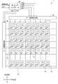
図1は、本実施形態に係る液晶表示装置の概略構成を示す平面図である。液晶表示装置1は、画像を表示する表示パネル10と、表示パネル10を駆動する駆動回路(データ線駆動回路20、ゲート線駆動回路30)と、駆動回路を制御するタイミングコントローラ40と、表示パネル10に背面側から光を照射するバックライト(図示せず)とを含んで構成されている。駆動回路は、表示パネル10に設けられてもよい。 FIG. 1 is a plan view showing a schematic configuration of the liquid crystal display device according to the present embodiment. The liquid crystal display device 1 includes a
図2は表示パネル10の一部の構成を示す平面図である。図3は図2のA−A´断面図であり、図4は図2のB−B´断面図である。図3に示すように、表示パネル10は、背面側に配置される薄膜トランジスタ基板100(以下、TFT基板という。)と、前面側(表示面側)に配置され、TFT基板100に対向するカラーフィルタ基板200(以下、CF基板という。)と、TFT基板100及びCF基板200の間に挟持される液晶層300と、を含んでいる。なお、図2は便宜上、前面側から、CF基板200を透視し、TFT基板100を見た状態を示している。 FIG. 2 is a plan view showing a partial configuration of the
図1及び図2に示すように、TFT基板100には、第1方向(例えば列方向)に延在する複数のデータ線11と、第1方向とは異なる第2方向(例えば行方向)に延在する複数のゲート線12とが形成され、複数のデータ線11と複数のゲート線12とのそれぞれの交差部近傍に薄膜トランジスタ13(以下、TFTという。)が形成され、隣り合う2本のデータ線11と隣り合う2本のゲート線12とにより囲まれる矩形領域が1つの画素14として規定され、該画素14がマトリクス状(行方向及び列方向)に複数配置されている。複数のデータ線11は、行方向に等間隔で配置されており、複数のゲート線12は、列方向に等間隔で配置されている。各画素14には画素電極15が設けられている。図2に示すように、各画素電極15は、開口部(例えばスリット)を有し、ストライプ状に形成されている。またTFT基板100には、各画素14に共通する1つの共通電極22(図3及び図4参照)が形成されており、共通電極22上には複数の共通電極配線21が形成されている。複数の共通電極配線21は、第1方向(例えば列方向)に延在し、第2方向(例えば行方向)に等間隔で配置されている。TFT13は、ゲート絶縁膜103(図3及び図4参照)上に、非晶質シリコン(a−Si)からなる半導体層18が形成され、半導体層18上にドレイン電極16及びソース電極17が形成されている。ドレイン電極16はデータ線11に電気的に接続され、ソース電極17と画素電極15とはコンタクトホール19を介して電気的に接続されている。 As shown in FIGS. 1 and 2, the
各データ線11には、データ線駆動回路20からデータ信号(データ電圧)が供給され、各ゲート線12には、ゲート線駆動回路30からゲート信号(ゲート電圧)が供給される。共通電極22には、複数の共通電極配線21(図3及び図4参照)を介して共通電圧Vcomが供給される。ゲート信号のオン電圧(ゲートオン電圧)がゲート線12に供給されると、ゲート線12に接続されたTFT13がオンし、TFT13に接続されたデータ線11を介して、データ電圧が画素電極15に供給される。画素電極15に供給されたデータ電圧と、共通電極22に供給された共通電圧Vcomとの差により電界が生じる。この電界により液晶を駆動してバックライトの光の透過率を制御することによって画像表示を行う。なお、カラー表示を行う場合は、ストライプ状の着色部で形成された赤色、緑色、青色に対応するそれぞれの画素14の画素電極15に接続されたそれぞれのデータ線11に、所望のデータ電圧を供給することにより実現される。 Each
図4に示すように、CF基板200には、各画素14に対応して複数の着色部202が形成されている。各着色部202は、光の透過を遮断するブラックマトリクス203で囲まれており、例えば矩形状に形成されている。また、複数の着色部202は、赤色(R色)の材料で形成され、赤色の光を透過する赤色部202Rと、緑色(G色)の材料で形成され、緑色の光を透過する緑色部202Gと、青色(B色)の材料で形成され、青色の光を透過する青色部202Bと、を含んでいる。赤色部202R、緑色部202G、及び青色部202Bは、行方向にこの順に繰り返し配列され、同一色の着色部202が列方向に配列され、行方向及び列方向に隣り合う着色部202の境界部分にブラックマトリクス203が形成されている。 As shown in FIG. 4, a plurality of colored portions 202 are formed on the
図1及び図2に示すように、複数の画素14は、赤色部202Rに対応する赤色画素14Rと、緑色部202Gに対応する緑色画素14Gと、青色部202Bに対応する青色画素14Bと、を含んでいる。また、これらの画素14は着色部202の配置に対応して配列されており、赤色画素14R、緑色画素14G、及び青色画素14Bが行方向にこの順に繰り返し配列され、同一色の画素14が列方向に配列されている。 As shown in FIGS. 1 and 2, the plurality of
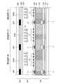
次に、図3及び図4を用いて、画素14の断面構造について具体的に説明する。図3は、図2においてTFT13を含む領域を行方向に切断した断面を示し、図4は、図2において画素14の開口領域を行方向に切断した断面を示している。 Next, the cross-sectional structure of the
図3を参照すると、TFT基板100において、ガラス基板101上にゲート線12が形成されている。ゲート線12は、アルミニウムAl、モリブデンMo、チタンTiあるいは銅Cuを主成分とする金属材料、又は上記の複数の積層層、又は上記金属材料にタングステンW、マンガンMnあるいはチタンTiなどが添加された合金、又は上記の組み合わせにおける積層金属層から形成される。 Referring to FIG. 3, the
ゲート線12を覆うように、ゲート絶縁膜103が形成されている。ゲート絶縁膜103の材料としては、シリコンナイトライドSiNを用いることができる。ゲート絶縁膜103上には半導体層18が形成されている。半導体層18上には、データ線11と、TFT13を構成するドレイン電極16及びソース電極17とが形成されている。ドレイン電極16は、データ線11に電気的に接続されている。 A
データ線11とドレイン電極16とソース電極17とを覆うように、層間絶縁膜104が形成されている。層間絶縁膜104の材料としては、シリコンナイトライドSiN又は二酸化シリコンSiO2を用いることができる。An interlayer insulating
層間絶縁膜104上には、有機絶縁膜105が形成されている。有機絶縁膜105の材料としては、アクリルを主成分とする感光性の有機材料を用いることができる。有機材料は、例えば比誘電率が4以下であり、シリコンナイトライドSiNの6.7に比べて低い。また製法上、有機材料は、シリコンナイトライドSiNに比べて厚く成膜することができる。有機絶縁膜105の厚さは、例えば1.5μmから3μmに設定されている。比誘電率を低く、かつ膜厚を厚くすることができるため、有機絶縁膜105の上に配置される共通電極22と、有機絶縁膜105の下に配置されるデータ線11又はゲート線12との間に形成される配線容量を大幅に低減することができる。 An organic insulating
有機絶縁膜105の上には、共通電極22が形成されている。共通電極22は、透明の電極材料ITOで構成されている。共通電極22の材料としては、例えば、インジウム・錫・酸化物や、インジウム・亜鉛・酸化物を用いることができる。各画素14の領域は、TFT13が形成される領域を除いて、共通電極22に覆われている。すなわち、共通電極22は、データ線11を覆っており、シールド電極としての機能を有している。これにより、例えばデータ線11から発せられる電界ノイズが液晶層300へ侵入することを防止することができる。共通電極22の上には、共通電極22に共通電圧Vcomを供給する共通電極配線21が形成されている。 A
共通電極22及び共通電極配線21を覆うように、上層絶縁膜106が形成されている。上層絶縁膜106の材料としては、シリコンナイトライドSiNを用いることができる。上層絶縁膜106の上には、画素電極15が形成されている。画素電極15は、透明の電極材料ITOで構成されている。画素電極15は、層間絶縁膜104及び上層絶縁膜106に形成されたコンタクトホール19を介して、ソース電極17に電気的に接続されている。図示はしていないが、画素電極15を覆うように配向膜が形成されており、ガラス基板101の外側には偏光板が形成されている。なお、図3及び図4に示す構成では、共通電極22が下層に配置され、画素電極15が上層に配置されているが、画素電極15が下層に配置され、共通電極22が上層に配置されてもよい。また、有機絶縁膜105が省略されていてもよい。 An upper insulating
CF基板200において、ガラス基板201上に着色部202(図4参照)とブラックマトリクス203とが形成されている。着色部202は、例えば赤色、緑色及び青色の顔料分散レジストによる着色層により形成されており、ブラックマトリクス203は、黒色の顔料を用いた樹脂材料あるいは金属材料で形成されている。着色部202及びブラックマトリクス203を覆うようにオーバーコート膜204が形成されており、オーバーコート膜204の上に配向膜205が形成されている。図示はしないが、ガラス基板201の外側には偏光板が形成されている。 In the
液晶層300は、正の誘電率異方性を有する液晶分子301(ポジ型液晶)を含む。 The
上記の例では、横電界方式の一例としてIPS方式を挙げたが、これに限定されない。また、画素14を構成する各部の積層構造は、上記の構成に限定されない。例えば、画素電極15及び共通電極22が櫛歯形状を有し同層に配置されてもよい。 In the above example, the IPS method is given as an example of the horizontal electric field method, but the present invention is not limited to this. Further, the stacked structure of each part constituting the
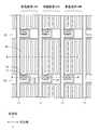
図5は、液晶表示装置1における各画素14に印加されるデータ電圧の極性の状態を示す図である。図5に示すように、各画素14に印加されるデータ電圧の極性は、1列ごとに反転する。また、図示はしないが、各データ電圧の極性は、1フレームごとに反転する。すなわち、液晶表示装置1は、列ライン反転駆動(カラム反転駆動ともいう。)を行う。列ライン反転駆動は、共通電圧Vcomを固定しつつ、隣り合うデータ線11に供給するデータ信号の電圧極性を互いに異ならせるとともに、1フレームごとに該電圧極性を反転させる駆動方法である。 FIG. 5 is a diagram illustrating the polarity state of the data voltage applied to each
次に、隣り合う画素それぞれに印加されるデータ電圧の振幅の差の影響による表示輝度のばらつきについて、具体例を挙げて説明する。 Next, the display luminance variation due to the influence of the difference in the amplitude of the data voltage applied to each adjacent pixel will be described with a specific example.
例えば、列ライン反転駆動において、赤色画素(R画素)、緑色画素(G画素)及び青色画素(B画素)それぞれに印加されるデータ電圧Vnを最大値(例えば±5V)に設定して、表示画面全体に白画像を表示(図6参照)したときの表示輝度をW0とする。また、赤色画素に印加されるデータ電圧Vnを最大値(例えば±5V)に設定し、緑色画素及び青色画素に印加されるデータ電圧Vnを0Vに設定して、表示画面全体に赤画像を表示(図7参照)したときの表示輝度をWrとする。また、緑色画素に印加されるデータ電圧Vnを最大値(例えば±5V)に設定し、赤色画素及び青色画素に印加されるデータ電圧Vnを0Vに設定して、表示画面全体に緑画像を表示(図8参照)したときの表示輝度とWgとする。また、青色画素に印加されるデータ電圧Vnを最大値(例えば±5V)に設定し、赤色画素及び緑色画素に印加されるデータ電圧Vnを0Vに設定して、表示画面全体に青画像を表示(図9参照)したときの表示輝度をWbとする。 For example, in the column line inversion drive, the data voltage Vn applied to each of the red pixel (R pixel), the green pixel (G pixel), and the blue pixel (B pixel) is set to the maximum value (for example, ± 5 V) to display The display brightness when a white image is displayed on the entire screen (see FIG. 6) is W0. Further, the data voltage Vn applied to the red pixel is set to the maximum value (for example, ± 5 V), the data voltage Vn applied to the green pixel and the blue pixel is set to 0 V, and the red image is displayed on the entire display screen. Let Wr be the display luminance when (see FIG. 7). Further, the data voltage Vn applied to the green pixel is set to the maximum value (for example, ± 5 V), the data voltage Vn applied to the red pixel and the blue pixel is set to 0 V, and the green image is displayed on the entire display screen. The display brightness and Wg when (see FIG. 8) are set. Further, the data voltage Vn applied to the blue pixel is set to the maximum value (for example, ± 5 V), the data voltage Vn applied to the red pixel and the green pixel is set to 0 V, and the blue image is displayed on the entire display screen. The display brightness when (see FIG. 9) is Wb.
理想的には、白画像の表示輝度(白色輝度)W0は、赤画像の表示輝度(赤色輝度)Wrと緑画像の表示輝度(緑色輝度)Wgと青画像の表示輝度(青色輝度)Wbとの合計(単色合計輝度Wrgb)に等しくなる(W0=Wr+Wg+Wb)。しかし、横電界方式の液晶表示装置にポジ型液晶を用いた場合において、白画像を表示する場合(図10(a)参照)は、単色画像を表示する場合(図10(b)参照)と比較して、隣り合う画素それぞれに印加されるデータ電圧の振幅の差(電圧差)が大きくなり、上記振幅の差に応じた電界により、隣り合う画素の境界部分の液晶のチルト角も大きくなる。このため、白画像を表示する場合は、各画素の透過率が低下し、表示輝度が低下する。すなわち、白色輝度W0が、単色合計輝度Wrgbより低くなる(W0<Wr+Wg+Wb)。 Ideally, the display brightness (white brightness) W0 of the white image includes the display brightness (red brightness) Wr of the red image, the display brightness (green brightness) Wg of the green image, and the display brightness (blue brightness) Wb of the blue image. (W0 = Wr + Wg + Wb). However, when a positive liquid crystal is used in a horizontal electric field type liquid crystal display device, when displaying a white image (see FIG. 10A), displaying a monochromatic image (see FIG. 10B). In comparison, the amplitude difference (voltage difference) of the data voltage applied to each adjacent pixel increases, and the tilt angle of the liquid crystal at the boundary portion between adjacent pixels also increases due to the electric field according to the amplitude difference. . For this reason, when displaying a white image, the transmittance | permeability of each pixel falls and a display brightness | luminance falls. That is, the white luminance W0 is lower than the monochromatic total luminance Wrgb (W0 <Wr + Wg + Wb).
図11は、入力階調と、白色輝度W0に対する、単色合計輝度Wrgb及び白色輝度W0の差の比((Wrgb−W0)/W0)との関係を示すグラフである。ここでは、入力階調を補正することなく、入力階調に応じた表示を行った場合の輝度の関係を示している。図11に示すように、入力階調が例えば150階調以上では、入力階調が高くなる程、輝度比が大きくなることが分かる。すなわち、入力階調が高くなる程、白色輝度W0と単色合計輝度Wrgbとの差が大きくなり、表示輝度のばらつきが大きくなることが分かる。このような表示輝度のばらつきは、表示品位の低下を招くおそれがある。 FIG. 11 is a graph showing the relationship between the input gradation and the ratio of the difference between the monochromatic total luminance Wrgb and the white luminance W0 ((Wrgb−W0) / W0) with respect to the white luminance W0. Here, the relationship of luminance is shown when display according to the input gradation is performed without correcting the input gradation. As shown in FIG. 11, when the input gradation is 150 gradations or more, for example, the luminance ratio increases as the input gradation increases. That is, it can be seen that the higher the input gradation, the larger the difference between the white luminance W0 and the single color total luminance Wrgb, and the larger the display luminance variation. Such variations in display luminance may cause a reduction in display quality.
これに対し、本実施形態に係る液晶表示装置1は、上記表示輝度のばらつきを低減する構成を有している。図12及び図13を用いて、具体的な構成について説明する。 On the other hand, the liquid crystal display device 1 according to the present embodiment has a configuration that reduces the variation in the display luminance. A specific configuration will be described with reference to FIGS.
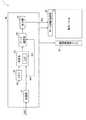
図12は、タイミングコントローラ40の具体的な構成を示すブロック図である。タイミングコントローラ40は、受信部41と、メモリ42と、決定部43と、データ補正部44と、出力部45とを含む。受信部41は、外部のシステム(図示せず)から映像信号DATを受信する。なお受信部41は、映像信号DATに含まれる、時間的に前後に配置された画素単位のデータ(画素データdat)を順次受信する。メモリ42は、受信した画素データdatを記憶する。決定部43は、受信した画素データdatに対する補正値を決定する。データ補正部44は、決定した補正値に基づいて画素データdatを補正する。出力部45は、画素データdatをデータ線駆動回路20に出力する。タイミングコントローラ40は、その他周知の画像処理を実行する。例えばタイミングコントローラ40は、外部のシステムから供給される映像信号と制御信号(クロック信号、垂直同期信号、水平同期信号)等に基づいて、データ線11に供給されるデータ電圧の極性を決定するための極性信号POLと、データ線駆動回路20及びゲート線駆動回路30の駆動を制御するための各種タイミング信号(データスタートパルスDSP、データクロックDCK、ゲートスタートパルスGSP、ゲートクロックGCK)とを生成する(図1参照)。 FIG. 12 is a block diagram showing a specific configuration of the
ここでは一例として、行方向に隣り合う2つの画素14を挙げる。それぞれの画素14に印加されるそれぞれの画素データdatは、映像信号DATにおいて時間的に前後に配置される。2つの画素データdatのうち先に受信される画素データdatを前画素データdat1と称し、前画素データdat1の次に受信される画素データdatを現画素データdat2と称す。 Here, as an example, two
先ず、前画素データdat1が受信部41に受信されると、前画素データdat1はメモリ42に記憶されるとともに、前画素データdat1の入力階調は補正されることなく、入力階調に応じた前画素データdat1が、出力部45からデータ線駆動回路20に出力される。 First, when the previous pixel data dat1 is received by the receiving
次に、現画素データdat2が受信部41に受信されると、決定部43は、メモリ42から前画素データdat1を取得し、受信部41から現画素データdat2を取得する。決定部43は、前画素データdat1及び現画素データdat2を比較して、ルックアップテーブル(LUT)431を参照して、現画素データdat2の補正値を決定する。決定部43は、比較部としての機能も有する。図13は、LUT431の一例を示す図である。LUT431には、映像信号DATにおける前画素データdat1の階調(入力階調)と、映像信号DATにおける現画素データdat2の階調(入力階調)と、現画素データdat2の補正階調Dnとが関連付けられている。現画素データdat2の補正階調Dnは、現画素データdat2の入力階調より低い階調に設定されている。例えば、LUT431には、現画素データdat2の入力階調が150階調以上で、かつ前画素データdat1の入力階調との差が150階調以上の範囲に、補正階調Dnが設定されている。また、補正階調Dnは、現画素データdat2の入力階調と前画素データdat1の入力階調との差が大きくなる程、補正量が大きくなるように設定されている。例えば、現画素データdat2の入力階調が160階調で、前画素データdat1の入力階調が0階調の場合は、補正階調Da1(<160階調)が設定されている。また現画素データdat2の入力階調が192階調で、前画素データdat1の入力階調が32階調,0階調の場合は、補正階調Db1(<192階調),Db2(<Db1)が設定されている。また現画素データdat2の入力階調が224階調で、前画素データdat1の入力階調が64階調,32階調,0階調の場合は、補正階調Dc1(<224階調),Dc2(<Dc1),Dc3(<Dc2)が設定されている。また現画素データdat2の入力階調が255階調で、前画素データdat1の入力階調が128階調,64階調,32階調,0階調の場合は、補正階調Dd1(<255階調),Dd2(<Dd1),Dd3(<Dd2),Dd4(<Dd3)が設定されている。 Next, when the current pixel data dat2 is received by the
決定部43が現画素データdat2の補正値(補正階調)を決定すると、データ補正部44は、補正値に基づいて現画素データdat2を補正する。具体的には、データ補正部44は、現画素データdat2の入力階調を補正階調に補正する。例えば、単色表示の場合(例えば図7及び図10(b)参照)、すなわち前画素データdat1の入力階調が0階調で、現画素データdat2の入力階調が255階調の場合、データ補正部44は、現画素データdat2を255階調より低い階調の補正階調Dd4(<255)に補正する。 When the
出力部45は、現画素データdat2の補正階調に応じたデータ電圧DAをデータ線駆動回路20に出力する。 The
上記構成によれば、例えば、図7〜図9に示すような単色表示を行う場合、すなわち、隣り合う2つの画素の一方が低階調、他方が高階調で、互いの階調差が所定値より大きい場合に、高階調の方を低く補正することにより、表示輝度を下げることができる。これにより、赤画像の表示輝度(赤色輝度)Wrと緑画像の表示輝度(緑色輝度)Wgと青画像の表示輝度(青色輝度)Wbのそれぞれを下げることができ、これらの合計輝度(単色合計輝度Wrgb)を、白画像の表示輝度(白色輝度)W0に近づけることができる(W0≒Wr+Wg+Wb)。よって、表示輝度のばらつきを低減できるため、表示品位の低下を抑えることができる。 According to the above configuration, for example, when performing monochromatic display as shown in FIGS. 7 to 9, that is, one of two adjacent pixels has a low gradation and the other has a high gradation, and the gradation difference between them is predetermined. When the value is larger than the value, the display luminance can be lowered by correcting the high gradation lower. Thereby, the display luminance (red luminance) Wr of the red image, the display luminance (green luminance) Wg of the green image, and the display luminance (blue luminance) Wb of the blue image can be lowered, and the total luminance (monochromatic total) The luminance Wrgb) can be made close to the display luminance (white luminance) W0 of the white image (W0≈Wr + Wg + Wb). Therefore, variation in display luminance can be reduced, so that deterioration in display quality can be suppressed.
タイミングコントローラ40の構成は図12に示す構成に限定されない。例えば、データ補正部44は、現画素データdat2と、前画素データdat1とを比較するだけでなく、さらに現画素データdat2と、次の画素データdat1とを比較して、現画素データdat2の補正をしてもよい。つまり、対象となる画素の入力階調を、該画素と左右または上下に隣接する2つの画素に入力される画素データと比較して、補正してもよい。また決定部43は、演算処理により上記補正値を算出してもよい。この場合、LUT431を省略することができる。また例えば、タイミングコントローラ40は、メモリ42が省略され、遅延回路を含んでもよい。この場合、遅延回路が前画素データdat1と現画素データdat2の転送タイミングを調整して、後段の決定部43及びデータ補正部44が各処理を実行すればよい。またタイミングコントローラ40が備える上記データ補正処理は、データ線駆動回路20の内部で行われてもよい。 The configuration of the
以上のように、本実施形態に係る液晶表示装置1では、1つの赤色画素14R、1つの緑色画素14G及び1つの青色画素14Bからなる表示画素14において、赤色画素14R、緑色画素14Gおよび青色画素14Bそれぞれに最高階調の信号を入力して白画像を表示する場合は、第1電圧レベルを有する第1データ電圧を赤色画素14R、緑色画素14G及び青色画素14Bそれぞれに接続される各データ線11に供給する。これに対して、表示画素14において、赤色画素14Rに最高階調の信号を入力し、かつ緑色画素14G及び青色画素14Bに最低階調の信号を入力して赤色の単色画像を表示する場合は、上記第1電圧レベルより低い電圧レベルを有するデータ電圧を赤色画素14Rに接続されるデータ線11に供給する。同様に、表示画素14において、緑色画素14Gに最高階調の信号を入力し、かつ赤色画素14R及び青色画素14Bに最低階調の信号を入力して緑色の単色画像を表示する場合は、上記第1電圧レベルより低い電圧レベルを有するデータ電圧を緑色画素14Gに接続されるデータ線11に供給する。同様に、表示画素14において、青色画素14Bに最高階調の信号を入力し、かつ赤色画素14R及び緑色画素14Gに最低階調の信号を入力して青色の単色画像を表示する場合は、上記第1電圧レベルより低い電圧レベルを有するデータ電圧を青色画素14Bに接続されるデータ線11に供給する。 As described above, in the liquid crystal display device 1 according to the present embodiment, in the
以上、本発明の実施形態について説明したが、本発明は上記各実施形態に限定されるものではなく、本発明の趣旨を逸脱しない範囲内で上記各実施形態から当業者が適宜変更した形態も本発明の技術的範囲に含まれることは言うまでもない。 As mentioned above, although embodiment of this invention was described, this invention is not limited to said each embodiment, The form suitably changed by those skilled in the art from said each embodiment within the range which does not deviate from the meaning of this invention. Needless to say, it is included in the technical scope of the present invention.
1 液晶表示装置、10 表示パネル、100 TFT基板、200 CF基板、300 液晶層、301 液晶分子、11 データ線、12 ゲート線、13 TFT、14 画素、14R 赤色画素、14G 緑色画素、14B 青色画素、15 画素電極、16 ドレイン電極、17 ソース電極、18 半導体層、19 コンタクトホール、20 共通電極、21 共通電極配線、103 ゲート絶縁膜、104 層間絶縁膜、105 有機絶縁膜、106 上層絶縁膜、202 着色部、202R 赤色部、202G 緑色部、202B 青色部、203 ブラックマトリクス、40 タイミングコントローラ、41 受信部、42 メモリ、43 決定部、431 LUT、44 データ補正部、45 出力部。 DESCRIPTION OF SYMBOLS 1 Liquid crystal display device, 10 Display panel, 100 TFT substrate, 200 CF substrate, 300 Liquid crystal layer, 301 Liquid crystal molecule, 11 Data line, 12 Gate line, 13 TFT, 14 pixel, 14R Red pixel, 14G Green pixel,
Claims (7)
Translated fromJapanese前記第1基板に対向配置された第2基板と、
前記第1基板及び前記第2基板の間に配置され、正の誘電率異方性を有する液晶分子を含む液晶層と、
を含み、
互いに隣り合う第1画素及び第2画素において、
入力映像信号における前記第1画素に印加される第1データ電圧が、前記入力映像信号における前記第2画素に印加される第2データ電圧より高い場合は、前記第1データ電圧を低く補正した第1補正データ電圧を前記第1画素に印加する、
ことを特徴とする液晶表示装置。A first substrate including a pixel electrode and a common electrode;
A second substrate disposed opposite the first substrate;
A liquid crystal layer including liquid crystal molecules disposed between the first substrate and the second substrate and having positive dielectric anisotropy;
Including
In the first pixel and the second pixel adjacent to each other,
When the first data voltage applied to the first pixel in the input video signal is higher than the second data voltage applied to the second pixel in the input video signal, the first data voltage is corrected to be lower. One correction data voltage is applied to the first pixel;
A liquid crystal display device characterized by the above.
ことを特徴とする請求項1に記載の液晶表示装置。Correcting the first data voltage to the first corrected data voltage when a difference between the first data voltage and the second data voltage is higher than a predetermined value;
The liquid crystal display device according to claim 1.
ことを特徴とする請求項1に記載の液晶表示装置。When the first data voltage is higher than the second data voltage and the polarity of the first data voltage and the polarity of the second data voltage are different from each other, the first data voltage is changed to the first correction data voltage. To correct,
The liquid crystal display device according to claim 1.
ことを特徴とする請求項1に記載の液晶表示装置。The first input gradation corresponding to the first pixel in the input video signal is higher than the second input gradation corresponding to the second pixel in the input video signal, and the first input gradation and the second input When the difference from the gray level is higher than the predetermined gray level, a data voltage corresponding to the first corrected gray level corrected to be lower than the first input gray level is applied to the first pixel;
The liquid crystal display device according to claim 1.
前記第1入力階調が前記第2入力階調より高く、前記第1入力階調と前記第2入力階調との差が所定階調より高い場合に、前記第1入力階調を、前記第1入力階調より低い階調の第1補正階調に補正する補正部と、
をさらに含む、ことを特徴とする請求項1に記載の液晶表示装置。A comparison unit that compares a first input gradation corresponding to the first pixel in the input video signal and a second input gradation corresponding to the second pixel in the input video signal;
When the first input gradation is higher than the second input gradation and the difference between the first input gradation and the second input gradation is higher than a predetermined gradation, the first input gradation is A correction unit that corrects to a first correction gradation having a gradation lower than the first input gradation;
The liquid crystal display device according to claim 1, further comprising:
前記ルックアップテーブルを参照して前記第1補正階調に決定する決定部と、をさらに含み、
前記補正部は、前記第1入力階調を、前記決定部により決定された前記第1補正階調に補正する、
ことを特徴とする請求項5に記載の液晶表示装置。A lookup table in which the first input gradation, the second input gradation, and the first correction gradation are associated;
A determination unit that determines the first correction gradation with reference to the lookup table;
The correction unit corrects the first input gradation to the first correction gradation determined by the determination unit;
The liquid crystal display device according to claim 5.
前記第1基板に対向配置された第2基板と、
前記第1基板及び前記第2基板の間に配置され、正の誘電率異方性を有する液晶分子を含む液晶層と、
を含み、
1つの赤色画素、1つの緑色画素及び1つの青色画素からなる表示画素において、前記赤色画素、前記緑色画素および前記青色画素それぞれに最高階調の信号を入力して白画像を表示する場合は、第1電圧レベルを有する第1データ電圧を前記赤色画素に接続されるデータ線に供給し、
前記表示画素において、前記赤色画素に前記最高階調の信号を入力し、かつ前記緑色画素及び前記青色画素に最低階調の信号を入力して赤色の単色画像を表示する場合は、第2電圧レベルを有する第2データ電圧を前記赤色画素に接続されるデータ線に供給し、
前記第2電圧レベルは、前記第1電圧レベルより低く設定されている、
ことを特徴とする液晶表示装置。A first substrate including a pixel electrode and a common electrode;
A second substrate disposed opposite the first substrate;
A liquid crystal layer including liquid crystal molecules disposed between the first substrate and the second substrate and having positive dielectric anisotropy;
Including
In a display pixel composed of one red pixel, one green pixel and one blue pixel, when displaying a white image by inputting a signal of the highest gradation to each of the red pixel, the green pixel and the blue pixel, Supplying a first data voltage having a first voltage level to a data line connected to the red pixel;
In the display pixel, when the signal of the highest gradation is input to the red pixel and the signal of the lowest gradation is input to the green pixel and the blue pixel to display a red monochrome image, the second voltage Supplying a second data voltage having a level to a data line connected to the red pixel;
The second voltage level is set lower than the first voltage level;
A liquid crystal display device characterized by the above.
Priority Applications (2)
| Application Number | Priority Date | Filing Date | Title |
|---|---|---|---|
| JP2016060751AJP2017173624A (en) | 2016-03-24 | 2016-03-24 | Liquid crystal display device |
| US15/467,534US10223953B2 (en) | 2016-03-24 | 2017-03-23 | Liquid crystal display device with data voltage correction |
Applications Claiming Priority (1)
| Application Number | Priority Date | Filing Date | Title |
|---|---|---|---|
| JP2016060751AJP2017173624A (en) | 2016-03-24 | 2016-03-24 | Liquid crystal display device |
Publications (1)
| Publication Number | Publication Date |
|---|---|
| JP2017173624Atrue JP2017173624A (en) | 2017-09-28 |
Family
ID=59898134
Family Applications (1)
| Application Number | Title | Priority Date | Filing Date |
|---|---|---|---|
| JP2016060751APendingJP2017173624A (en) | 2016-03-24 | 2016-03-24 | Liquid crystal display device |
Country Status (2)
| Country | Link |
|---|---|
| US (1) | US10223953B2 (en) |
| JP (1) | JP2017173624A (en) |
Families Citing this family (5)
| Publication number | Priority date | Publication date | Assignee | Title |
|---|---|---|---|---|
| KR102653295B1 (en)* | 2016-08-25 | 2024-04-01 | 삼성디스플레이 주식회사 | Liquid crystal display device and driving method thereof |
| CN207396936U (en)* | 2017-10-24 | 2018-05-22 | 京东方科技集团股份有限公司 | A kind of array substrate and display device |
| CN108319012B (en)* | 2018-01-31 | 2020-06-30 | 京东方科技集团股份有限公司 | Display panel, display device and display method |
| CN111937495B (en)* | 2018-03-30 | 2023-08-15 | 夏普株式会社 | Display device |
| US11990078B1 (en)* | 2022-11-02 | 2024-05-21 | Innolux Corporation | Electronic device |
Family Cites Families (4)
| Publication number | Priority date | Publication date | Assignee | Title |
|---|---|---|---|---|
| US6727872B2 (en)* | 2001-01-22 | 2004-04-27 | Brillian Corporation | Image quality improvement for liquid crystal display |
| JP4356750B2 (en) | 2007-01-25 | 2009-11-04 | エプソンイメージングデバイス株式会社 | Liquid crystal display device and manufacturing method thereof |
| JP5229713B2 (en)* | 2007-01-29 | 2013-07-03 | 株式会社ジャパンディスプレイイースト | Display device |
| JP5353784B2 (en)* | 2010-03-19 | 2013-11-27 | カシオ計算機株式会社 | Liquid crystal display |
- 2016
- 2016-03-24JPJP2016060751Apatent/JP2017173624A/enactivePending
- 2017
- 2017-03-23USUS15/467,534patent/US10223953B2/enactiveActive
Also Published As
| Publication number | Publication date |
|---|---|
| US10223953B2 (en) | 2019-03-05 |
| US20170278446A1 (en) | 2017-09-28 |
Similar Documents
| Publication | Publication Date | Title |
|---|---|---|
| US9995952B2 (en) | Driving method of liquid crystal display panel | |
| JP3639830B2 (en) | Liquid crystal display | |
| WO2018121307A1 (en) | Liquid crystal display device | |
| CN105047167B (en) | A kind of source electrode drive circuit, display device and its driving method | |
| US10223953B2 (en) | Liquid crystal display device with data voltage correction | |
| JP2007164198A (en) | Liquid crystal display | |
| JPWO2010134439A1 (en) | LCD panel | |
| US20120105735A1 (en) | Active matrix substrate, liquid crystal panel, liquid crystal display device, liquid crystal display unit, and television receiver | |
| KR102764289B1 (en) | Liquid crystal display panel | |
| JP5179670B2 (en) | Liquid crystal display | |
| KR20090131039A (en) | Pixel driving method and display device for performing the same | |
| WO2011074497A1 (en) | Liquid crystal display device | |
| US10783841B2 (en) | Liquid crystal display device and method for displaying image of the same | |
| US10083662B2 (en) | Data processing method for transparent liquid crystal display | |
| US9786236B2 (en) | Liquid crystal panels and the driving methods thereof | |
| US10102812B2 (en) | Data processing method for transparent liquid crystal display | |
| US20130321497A1 (en) | Method of Signal Compensation, Transformation Circuit in Liquid Crystal Panel, and Liquid Crystal Display Device | |
| JP2006330609A (en) | Liquid crystal display | |
| KR102210677B1 (en) | Display device | |
| US20160133207A1 (en) | Display device and driving method thereof | |
| JP2009282109A (en) | Display element | |
| WO2011077802A1 (en) | Liquid crystal drive circuit, liquid crystal display device provided therewith, and drive method for liquid crystal drive circuit | |
| KR102524416B1 (en) | Display device | |
| CN101452169B (en) | Liquid crystal display panel and liquid crystal display device using same | |
| KR20160046981A (en) | Display panel |