JP2017152720A - Semiconductor device - Google Patents
Semiconductor deviceDownload PDFInfo
- Publication number
- JP2017152720A JP2017152720AJP2017076375AJP2017076375AJP2017152720AJP 2017152720 AJP2017152720 AJP 2017152720AJP 2017076375 AJP2017076375 AJP 2017076375AJP 2017076375 AJP2017076375 AJP 2017076375AJP 2017152720 AJP2017152720 AJP 2017152720A
- Authority
- JP
- Japan
- Prior art keywords
- film
- oxide semiconductor
- transistor
- oxide
- semiconductor film
- Prior art date
- Legal status (The legal status is an assumption and is not a legal conclusion. Google has not performed a legal analysis and makes no representation as to the accuracy of the status listed.)
- Granted
Links
Images


Classifications
- H—ELECTRICITY
- H10—SEMICONDUCTOR DEVICES; ELECTRIC SOLID-STATE DEVICES NOT OTHERWISE PROVIDED FOR
- H10D—INORGANIC ELECTRIC SEMICONDUCTOR DEVICES
- H10D30/00—Field-effect transistors [FET]
- H10D30/60—Insulated-gate field-effect transistors [IGFET]
- H10D30/67—Thin-film transistors [TFT]
- H10D30/674—Thin-film transistors [TFT] characterised by the active materials
- H10D30/6755—Oxide semiconductors, e.g. zinc oxide, copper aluminium oxide or cadmium stannate
- H—ELECTRICITY
- H10—SEMICONDUCTOR DEVICES; ELECTRIC SOLID-STATE DEVICES NOT OTHERWISE PROVIDED FOR
- H10D—INORGANIC ELECTRIC SEMICONDUCTOR DEVICES
- H10D30/00—Field-effect transistors [FET]
- H10D30/60—Insulated-gate field-effect transistors [IGFET]
- H10D30/67—Thin-film transistors [TFT]
- H10D30/6758—Thin-film transistors [TFT] characterised by the insulating substrates
- H—ELECTRICITY
- H10—SEMICONDUCTOR DEVICES; ELECTRIC SOLID-STATE DEVICES NOT OTHERWISE PROVIDED FOR
- H10D—INORGANIC ELECTRIC SEMICONDUCTOR DEVICES
- H10D62/00—Semiconductor bodies, or regions thereof, of devices having potential barriers
- H10D62/40—Crystalline structures
Landscapes
- Thin Film Transistor (AREA)
- Recrystallisation Techniques (AREA)
- Electroluminescent Light Sources (AREA)
- Physical Vapour Deposition (AREA)
- Semiconductor Memories (AREA)
- Non-Volatile Memory (AREA)
- Physical Deposition Of Substances That Are Components Of Semiconductor Devices (AREA)
- Metal-Oxide And Bipolar Metal-Oxide Semiconductor Integrated Circuits (AREA)
- Chemical & Material Sciences (AREA)
- Crystallography & Structural Chemistry (AREA)
- Devices For Indicating Variable Information By Combining Individual Elements (AREA)
Abstract
Translated fromJapaneseDescription
Translated fromJapanese半導体素子及び半導体素子の作製方法、並びに半導体素子を用いた半導体装置に関する。The present invention relates to a semiconductor element, a method for manufacturing the semiconductor element, and a semiconductor device using the semiconductor element.
なお、本明細書中において、「半導体素子」とは、トランジスタやダイオードなどの半導
体特性を利用することで機能しうる素子を指すものである。また、「半導体装置」とは、
半導体素子の半導体特性を利用することで機能しうる装置全般を指し、電気光学装置、半
導体回路および電子機器は全て半導体装置である。Note that in this specification, a “semiconductor element” refers to an element that can function by utilizing semiconductor characteristics such as a transistor or a diode. In addition, "semiconductor device"
It refers to all devices that can function by utilizing the semiconductor characteristics of semiconductor elements, and electro-optical devices, semiconductor circuits, and electronic devices are all semiconductor devices.
絶縁表面を有する基板上に形成された半導体薄膜を用いてトランジスタを構成する技術が
注目されている。該トランジスタは集積回路(IC)や画像表示装置(表示装置)のよう
な電子デバイスに広く応用されている。トランジスタに適用可能な半導体薄膜としてシリ
コン系半導体材料が広く知られているが、その他の材料として酸化物半導体が注目されて
いる。A technique for forming a transistor using a semiconductor thin film formed over a substrate having an insulating surface has attracted attention. The transistor is widely applied to electronic devices such as an integrated circuit (IC) and an image display device (display device). A silicon-based semiconductor material is widely known as a semiconductor thin film applicable to a transistor, but an oxide semiconductor has attracted attention as another material.
例えば、トランジスタの活性層として、インジウム(In)、ガリウム(Ga)、及び亜
鉛(Zn)を含む非晶質の酸化物半導体膜を用いたトランジスタが開示されている(特許
文献1参照)。For example, a transistor using an amorphous oxide semiconductor film containing indium (In), gallium (Ga), and zinc (Zn) as an active layer of the transistor is disclosed (see Patent Document 1).
活性層として酸化物半導体膜を用いたトランジスタ(以下、酸化物半導体トランジスタと
呼称する。)は、活性層としてアモルファスシリコン膜を用いたトランジスタよりも動作
が速く(電界効果移動度が高い、とも言える。)、また、活性層として多結晶シリコン膜
を用いたトランジスタよりも製造が容易であるといった特徴を有している。A transistor using an oxide semiconductor film as an active layer (hereinafter referred to as an oxide semiconductor transistor) operates faster (has higher field-effect mobility) than a transistor using an amorphous silicon film as an active layer. In addition, it has a feature that it is easier to manufacture than a transistor using a polycrystalline silicon film as an active layer.
その反面、活性層として酸化物半導体膜を用いたトランジスタは幾つかの問題が指摘され
ており、その一つとして電気的特性の不安定さがある。具体的には、可視光または紫外光
の照射やバイアス−熱ストレス試験(BTストレス試験とも言われる。)においてトラン
ジスタのしきい値電圧がマイナス側にシフトし、トランジスタがノーマリーオンの傾向を
示すことが指摘されており、この原因の1つとして、酸化物半導体膜中の酸素欠損などが
挙げられる。On the other hand, a transistor using an oxide semiconductor film as an active layer has some problems, and one of them is instability of electrical characteristics. Specifically, the threshold voltage of a transistor shifts to the minus side in visible light or ultraviolet light irradiation or a bias-thermal stress test (also referred to as a BT stress test), and the transistor tends to be normally on. One of the causes is oxygen deficiency in the oxide semiconductor film.
酸化物半導体膜が非晶質(アモルファスとも言われる。)であると、酸化物半導体膜中の
金属原子と酸素原子の結合状態は秩序化されておらず、酸素欠損が生じやすい状態にある
といえる。そのため、酸化物半導体膜の電気的特性(例えば、電気伝導度など。)が変化
する恐れがある。そして、トランジスタの電気的特性の変動要因となり得るため、当該ト
ランジスタを用いた半導体装置の信頼性を低下させることになる。When the oxide semiconductor film is amorphous (also referred to as amorphous), the bonding state between metal atoms and oxygen atoms in the oxide semiconductor film is not ordered, and oxygen vacancies are likely to occur. I can say that. Therefore, the electrical characteristics (eg, electrical conductivity) of the oxide semiconductor film may change. Then, since it can be a factor of variation in the electrical characteristics of the transistor, the reliability of the semiconductor device using the transistor is reduced.
このような問題に鑑み、本発明の一態様では、活性層として酸化物半導体膜を用いた場合
においても、電気的特性の安定したトランジスタを提供することを課題の一つとする。ま
た、当該トランジスタの作製方法を提供することを課題の一つとする。また、当該トラン
ジスタを用いることにより、安定した電気的特性を付与し信頼性の高い半導体装置を提供
することを課題の一つとする。In view of such problems, an object of one embodiment of the present invention is to provide a transistor with stable electrical characteristics even when an oxide semiconductor film is used as an active layer. Another object is to provide a method for manufacturing the transistor. Another object is to provide a highly reliable semiconductor device with stable electric characteristics by using the transistor.
酸化物半導体膜を成膜する被形成面に、少なくとも表面が結晶性を有する酸化物膜が下地
膜として設けられ、当該膜上に酸化物半導体膜が設けられた構造とする。これにより、下
地膜は酸化物半導体膜の種結晶として機能する。そして、酸化物半導体膜は、下地膜との
界面近傍から、下地膜の結晶状態を反映して結晶成長する。このため、酸化物半導体膜は
膜厚方向の広い範囲において結晶性を有する膜となり、当該膜を有するトランジスタは、
電気的特性が安定したものとなる。A structure in which an oxide film having crystallinity at least on its surface is provided as a base film on a surface where the oxide semiconductor film is formed, and the oxide semiconductor film is provided over the oxide film. Thus, the base film functions as a seed crystal for the oxide semiconductor film. The oxide semiconductor film grows from the vicinity of the interface with the base film, reflecting the crystal state of the base film. Therefore, the oxide semiconductor film becomes a film having crystallinity in a wide range in the film thickness direction, and a transistor including the film has
The electrical characteristics are stable.
すなわち、本発明の一態様は、少なくとも表面が結晶性を有する酸化物膜である下地膜と
、下地膜上の結晶性を有する酸化物半導体膜と、酸化物半導体膜上のゲート絶縁膜と、ゲ
ート絶縁膜上の少なくとも酸化物半導体膜と重畳するゲート電極と、酸化物半導体膜と電
気的に接続するソース電極およびドレイン電極とを有し、下地膜はインジウムおよび亜鉛
を含むことを特徴とする半導体素子である。That is, according to one embodiment of the present invention, at least a base film whose surface is an oxide film having crystallinity, an oxide semiconductor film having crystallinity on the base film, a gate insulating film on the oxide semiconductor film, A gate electrode overlapping with at least the oxide semiconductor film over the gate insulating film; a source electrode and a drain electrode electrically connected to the oxide semiconductor film; and the base film containing indium and zinc It is a semiconductor element.
上述の一態様に示す構造を用いることにより、酸化物半導体膜は下地膜の結晶状態を反映
して結晶成長するため、酸化物半導体膜は膜厚方向の広い範囲において結晶性を有する膜
となる。したがって、当該膜を有するトランジスタの電気的特性を安定したものとするこ
とができる。With the use of the structure described in the above embodiment, the oxide semiconductor film grows by reflecting the crystal state of the base film, and thus the oxide semiconductor film has a crystallinity in a wide range in the film thickness direction. . Therefore, the electrical characteristics of the transistor including the film can be stabilized.
なお、上述の構造において、下地膜がインジウムおよび亜鉛を含み、かつ、ジルコニウム
、イットリウムまたはセリウムのいずれか一種以上を含むことにより、下地膜の導電率を
低減することができ、ソース電極およびドレイン電極間を流れるキャリアは下地膜に影響
を受けにくく好ましい。Note that in the above structure, when the base film contains indium and zinc and contains at least one of zirconium, yttrium, and cerium, the conductivity of the base film can be reduced, and the source electrode and the drain electrode can be reduced. Carriers flowing between them are preferable because they are not easily affected by the underlying film.
また、上述の構造において、酸化物半導体膜が、非晶質相に結晶部を有する結晶−非晶質
混相構造であり、結晶部はc軸が酸化物半導体膜の被形成面の法線ベクトルまたは酸化物
半導体膜の表面の法線ベクトルに平行な方向に揃い、かつab面に垂直な方向から見て三
角形状または六角形状の原子配列を有し、c軸に垂直な方向から見て金属原子が層状また
は金属原子と酸素原子とが層状に配列していることにより、当該酸化物半導体膜を用いた
トランジスタは安定した電気的特性を示すため好ましい。In the above structure, the oxide semiconductor film has a crystal-amorphous mixed phase structure in which a crystal part is included in an amorphous phase, and the c-axis of the crystal part is a normal vector of a formation surface of the oxide semiconductor film. Alternatively, the metal is aligned in the direction parallel to the normal vector of the surface of the oxide semiconductor film and has a triangular or hexagonal atomic arrangement when viewed from the direction perpendicular to the ab plane, and is viewed from the direction perpendicular to the c-axis. A transistor using the oxide semiconductor film is preferable because the atoms are arranged in layers or metal atoms and oxygen atoms are arranged in layers.
また、上述の構造を有する半導体素子を半導体装置の一部として用いることにより、当該
半導体装置を信頼性の高い半導体装置とすることができる。In addition, when a semiconductor element having the above structure is used as part of a semiconductor device, the semiconductor device can be a highly reliable semiconductor device.
また、本発明の一態様は、少なくとも表面が結晶性を有する酸化物膜である下地膜を形成
し、下地膜上に結晶性を有する酸化物半導体膜を形成し、酸化物半導体膜上にゲート絶縁
膜を形成しゲート絶縁膜上に少なくとも酸化物半導体膜と重畳するゲート電極を形成し、
酸化物半導体膜と電気的に接続するソース電極およびドレイン電極を形成する工程を有し
、下地膜として、インジウムおよび亜鉛を含む膜を形成することを特徴とする半導体素子
の作製方法である。According to one embodiment of the present invention, a base film which is an oxide film having crystallinity at least on the surface is formed, an oxide semiconductor film having crystallinity is formed over the base film, and a gate is formed over the oxide semiconductor film. Forming an insulating film and forming a gate electrode overlapping with at least the oxide semiconductor film on the gate insulating film;
A method for manufacturing a semiconductor element includes forming a source electrode and a drain electrode that are electrically connected to an oxide semiconductor film, and forming a film containing indium and zinc as a base film.
上述の一態様に示す作製方法を用いることにより、酸化物半導体膜は下地膜の結晶状態を
反映して結晶成長するため、膜厚方向の広い範囲において結晶性を有する酸化物半導体膜
を形成することができる。したがって、当該膜を有するトランジスタの電気的特性を安定
したものとすることができる。By using the manufacturing method described in the above embodiment, the oxide semiconductor film grows by reflecting the crystal state of the base film; thus, an oxide semiconductor film having crystallinity is formed in a wide range in the film thickness direction. be able to. Therefore, the electrical characteristics of the transistor including the film can be stabilized.
なお、上述の作製方法において、下地膜として、インジウムおよび亜鉛を含み、かつ、ジ
ルコニウム、イットリウムまたはセリウムのいずれか一種以上を含む膜を用いることによ
り、導電率の低い下地膜を形成することができるため、ソース電極およびドレイン電極間
を流れるキャリアは下地膜に影響を受けにくく好ましい。Note that in the above manufacturing method, a base film with low conductivity can be formed by using a film containing indium and zinc and containing at least one of zirconium, yttrium, and cerium as the base film. Therefore, it is preferable that carriers flowing between the source electrode and the drain electrode are less affected by the base film.
また、上述の作製方法において、酸化物半導体膜を、スパッタリング装置を用いて200
℃以上450℃以下の成膜温度において成膜することにより、被形成面または表面の法線
ベクトルに対してc軸が平行な方向に揃った結晶部を有する酸化物半導体膜を形成するこ
とができるため好ましい。In the above manufacturing method, the oxide semiconductor film is formed using a sputtering apparatus with a thickness of 200.
An oxide semiconductor film having a crystal part in which the c-axis is aligned in a direction parallel to the normal vector of the surface to be formed or the surface can be formed by forming the film at a film formation temperature of ° C to 450 ° C. This is preferable because it is possible.
また、上述の作製方法において、酸化物半導体膜を、スパッタリング装置を用いて成膜し
た後、前記酸化物半導体膜に対して200℃以上700℃以下の熱処理を行うことにより
、被形成面または表面の法線ベクトルに対してc軸が平行な方向に揃った結晶部を有する
酸化物半導体膜を形成することができるため好ましい。In the above manufacturing method, after the oxide semiconductor film is formed using a sputtering apparatus, heat treatment is performed at 200 ° C. to 700 ° C. with respect to the oxide semiconductor film. An oxide semiconductor film having a crystal part in which the c-axis is aligned in a direction parallel to the normal vector is preferable.
酸化物半導体膜を成膜する被形成面に、少なくとも表面が結晶性を有する酸化物膜が下地
膜として設けられ、当該下地膜上に酸化物半導体膜が設けられた構造とすることにより、
酸化物半導体膜は、下地膜の結晶状態を反映して、酸化物膜との界面近傍から結晶成長す
るため、酸化物半導体膜は膜厚方向の広い範囲において結晶性を有する膜となる。したが
って、当該膜を有するトランジスタの電気的特性を安定したものとすることができる。By providing a structure in which an oxide film having crystallinity at least on its surface is provided as a base film on a surface on which the oxide semiconductor film is formed, and the oxide semiconductor film is provided over the base film,
The oxide semiconductor film reflects a crystal state of the base film and grows from the vicinity of the interface with the oxide film. Therefore, the oxide semiconductor film has a crystallinity in a wide range in the film thickness direction. Therefore, the electrical characteristics of the transistor including the film can be stabilized.
以下では、本明細書に開示する発明の実施の形態について図面を用いて詳細に説明する。
但し、本発明は以下の説明に限定されず、本発明の趣旨およびその範囲から逸脱すること
なくその形態および詳細を様々に変更し得ることは当業者であれば容易に理解される。従
って、本発明は以下に示す実施の形態の記載内容に限定して解釈されるものではない。Hereinafter, embodiments of the invention disclosed in this specification will be described in detail with reference to the drawings.
However, the present invention is not limited to the following description, and it is easily understood by those skilled in the art that modes and details can be variously changed without departing from the spirit and scope of the present invention. Therefore, the present invention should not be construed as being limited to the description of the embodiments below.
以下に説明する実施の形態において、同一部分または同様な機能を有する部分には同一の
符号を異なる図面間で共通して用い、その繰り返しの説明は省略する場合がある。In the embodiments described below, the same portions or portions having similar functions are denoted by the same reference numerals in different drawings, and description thereof is not repeated.
なお、図面等において示す各構成の、位置、大きさ、範囲などは、理解の簡単のため、実
際の位置、大きさ、範囲などを表していない場合がある。このため、開示する発明は、必
ずしも、図面等に開示された位置、大きさ、範囲などに限定されない。Note that the position, size, range, and the like of each component illustrated in the drawings and the like may not represent the actual position, size, range, or the like for easy understanding. Therefore, the disclosed invention is not necessarily limited to the position, size, range, or the like disclosed in the drawings and the like.
また、本明細書等における「第1」、「第2」、「第3」などの序数は、構成要素の混同
を避けるために付すものであり、数的に限定するものではないことを付記する。In addition, ordinal numbers such as “first”, “second”, and “third” in this specification and the like are added to avoid confusion between components, and are not limited numerically. To do.
また、本明細書等において「上」や「下」の用語は、構成要素の位置関係が「直上」また
は「直下」であることを限定するものではない。例えば、「ゲート絶縁層上のゲート電極
」の表現であれば、ゲート絶縁層とゲート電極との間に他の構成要素を含むものを除外し
ない。Further, in this specification and the like, the terms “upper” and “lower” do not limit that the positional relationship between the constituent elements is “directly above” or “directly below”. For example, the expression “a gate electrode over a gate insulating layer” does not exclude the case where another component is included between the gate insulating layer and the gate electrode.
また、本明細書等において「電極」や「配線」の用語は、これらの構成要素を機能的に限
定するものではない。例えば、「電極」は「配線」の一部として用いられることがあり、
その逆もまた同様である。さらに、「電極」や「配線」の用語は、複数の「電極」や「配
線」が一体となって形成されている場合なども含む。Further, in this specification and the like, the terms “electrode” and “wiring” do not functionally limit these components. For example, an “electrode” may be used as part of a “wiring”
The reverse is also true. Furthermore, the terms “electrode” and “wiring” include a case where a plurality of “electrodes” and “wirings” are integrally formed.
また、「ソース」や「ドレイン」の機能は、異なる極性のトランジスタを採用する場合や
、回路動作において電流の方向が変化する場合などには入れ替わることがある。このため
、本明細書等においては、「ソース」や「ドレイン」の用語は、入れ替えて用いることが
できるものとする。In addition, the functions of “source” and “drain” may be switched when transistors having different polarities are employed or when the direction of current changes in circuit operation. Therefore, in this specification and the like, the terms “source” and “drain” can be used interchangeably.
また、本明細書等において、「電気的に接続」には、「何らかの電気的作用を有するもの
」を介して接続されている場合が含まれる。ここで、「何らかの電気的作用を有するもの
」は、接続対象間での電気信号の授受を可能とするものであれば、特に制限を受けない。
例えば、「何らかの電気的作用を有するもの」には、電極や配線をはじめ、トランジスタ
などのスイッチング素子、抵抗素子、インダクタ、キャパシタ、その他の各種機能を有す
る素子などが含まれる。In addition, in this specification and the like, “electrically connected” includes a case of being connected via “thing having some electric action”. Here, the “thing having some electric action” is not particularly limited as long as it can exchange electric signals between connection targets.
For example, “thing having some electric action” includes electrodes, wiring, switching elements such as transistors, resistance elements, inductors, capacitors, and other elements having various functions.
(実施の形態1)
本実施の形態では、半導体装置及び半導体装置の作製方法の一形態を、図1乃至図5を用
いて説明する。(Embodiment 1)
In this embodiment, one embodiment of a semiconductor device and a method for manufacturing the semiconductor device will be described with reference to FIGS.
<半導体装置の構成例>
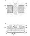
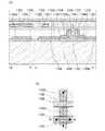
図1(A)および図1(B)に、半導体装置の例として、トップゲート構造のトランジス
タの平面図および断面図の一例を示す。図1(A)は平面図であり、図1(B)は、図1
(A)におけるA−B断面の断面図である。なお、図1(A)では、煩雑になることを避
けるため、トランジスタ150の構成要素の一部(例えば、基板100など)を省略して
いる。<Configuration example of semiconductor device>
1A and 1B illustrate an example of a plan view and a cross-sectional view of a top-gate transistor as an example of a semiconductor device. FIG. 1A is a plan view, and FIG.
It is sectional drawing of the AB cross section in (A). Note that in FIG. 1A, some components of the transistor 150 (e.g., the substrate 100) are omitted to avoid complexity.
図1(A)および図1(B)に示すトランジスタ150は、基板100上に、下地膜10
2と、酸化物半導体膜106と、ゲート絶縁膜108と、少なくとも酸化物半導体膜10
6と重畳するゲート電極110と、酸化物半導体膜106と電気的に接続するソース電極
114aおよびドレイン電極114bを有している。A
2, the
6, and a
酸化物半導体膜106に用いる酸化物半導体としては、インジウム(In)および亜鉛(
Zn)を含むことが好ましい。また、該酸化物半導体を用いたトランジスタの電気的特性
のばらつきを減らすためのスタビライザーとして、それらに加えてガリウム(Ga)を有
することが好ましい。また、スタビライザーとしてスズ(Sn)を有することが好ましい
。また、スタビライザーとしてハフニウム(Hf)、ジルコニウム(Zr)、チタン(T
i)、スカンジウム(Sc)、イットリウム(Y)、ランタノイド(例えば、セリウム(
Ce)、ネオジム(Nd)、ガドリニウム(Gd))から選ばれた一種又は複数種が含ま
れていることが好ましい。As an oxide semiconductor used for the
Zn) is preferably included. In addition, it is preferable that gallium (Ga) be included in addition to the stabilizer for reducing variation in electrical characteristics of the transistor including the oxide semiconductor. Moreover, it is preferable to have tin (Sn) as a stabilizer. As stabilizers, hafnium (Hf), zirconium (Zr), titanium (T
i), scandium (Sc), yttrium (Y), lanthanoids (eg, cerium (
Preferably, one or more selected from Ce), neodymium (Nd), and gadolinium (Gd)) are included.
例えば、酸化物半導体として、酸化インジウム、酸化スズ、酸化亜鉛、In−Zn系酸化
物、Sn−Zn系酸化物、Al−Zn系酸化物、Zn−Mg系酸化物、Sn−Mg系酸化
物、In−Mg系酸化物、In−Ga系酸化物、In−Ga−Zn系酸化物(IGZOと
も表記する)、In−Al−Zn系酸化物、In−Sn−Zn系酸化物、Sn−Ga−Z
n系酸化物、Al−Ga−Zn系酸化物、Sn−Al−Zn系酸化物、In−Hf−Zn
系酸化物、In−Zr−Zn系酸化物、In−Ti−Zn系酸化物、In−Sc−Zn系
酸化物、In−Y−Zn系酸化物、In−La−Zn系酸化物、In−Ce−Zn系酸化
物、In−Pr−Zn系酸化物、In−Nd−Zn系酸化物、In−Sm−Zn系酸化物
、In−Eu−Zn系酸化物、In−Gd−Zn系酸化物、In−Tb−Zn系酸化物、
In−Dy−Zn系酸化物、In−Ho−Zn系酸化物、In−Er−Zn系酸化物、I
n−Tm−Zn系酸化物、In−Yb−Zn系酸化物、In−Lu−Zn系酸化物、In
−Sn−Ga−Zn系酸化物、In−Hf−Ga−Zn系酸化物、In−Al−Ga−Z
n系酸化物、In−Sn−Al−Zn系酸化物、In−Sn−Hf−Zn系酸化物、In
−Hf−Al−Zn系酸化物を用いることができる。For example, as an oxide semiconductor, indium oxide, tin oxide, zinc oxide, In—Zn oxide, Sn—Zn oxide, Al—Zn oxide, Zn—Mg oxide, Sn—Mg oxide In-Mg-based oxide, In-Ga-based oxide, In-Ga-Zn-based oxide (also referred to as IGZO), In-Al-Zn-based oxide, In-Sn-Zn-based oxide, Sn- Ga-Z
n-based oxide, Al-Ga-Zn-based oxide, Sn-Al-Zn-based oxide, In-Hf-Zn
Oxide, In—Zr—Zn oxide, In—Ti—Zn oxide, In—Sc—Zn oxide, In—Y—Zn oxide, In—La—Zn oxide, In -Ce-Zn oxide, In-Pr-Zn oxide, In-Nd-Zn oxide, In-Sm-Zn oxide, In-Eu-Zn oxide, In-Gd-Zn oxide Oxide, In-Tb-Zn-based oxide,
In-Dy-Zn-based oxide, In-Ho-Zn-based oxide, In-Er-Zn-based oxide, I
n-Tm-Zn-based oxide, In-Yb-Zn-based oxide, In-Lu-Zn-based oxide, In
-Sn-Ga-Zn-based oxide, In-Hf-Ga-Zn-based oxide, In-Al-Ga-Z
n-based oxide, In-Sn-Al-Zn-based oxide, In-Sn-Hf-Zn-based oxide, In
A —Hf—Al—Zn-based oxide can be used.
ここで、In−Ga−Zn系酸化物とは、InとGaとZnを主成分として有する酸化物
という意味であり、InとGaとZnの比率は問わない。また、InとGaとZn以外の
金属元素が入っていてもよい。In−Ga−Zn系酸化物は、無電界時の抵抗が十分に高
くオフ電流を十分に小さくすることが可能であり、また、移動度も高いため、半導体装置
に用いる半導体材料としては好適である。Here, the In—Ga—Zn-based oxide means an oxide containing In, Ga, and Zn as main components, and there is no limitation on the ratio of In, Ga, and Zn. Moreover, metal elements other than In, Ga, and Zn may be contained. An In—Ga—Zn-based oxide has a sufficiently high resistance in the absence of an electric field and can have a sufficiently low off-state current. Also, since it has high mobility, it is suitable as a semiconductor material used for a semiconductor device. is there.
例えば、In:Ga:Zn=1:1:1(=1/3:1/3:1/3)、In:Ga:Z
n=3:1:2(=1/2:1/6:1/3)、In:Ga:Zn=1:3:2(=1/
6:1/2:1/3)あるいはIn:Ga:Zn=2:2:1(=2/5:2/5:1/
5)の原子比のIn−Ga−Zn系酸化物やその組成の近傍の酸化物を用いることができ
る。あるいは、In:Sn:Zn=1:1:1(=1/3:1/3:1/3)、In:S
n:Zn=2:1:3(=1/3:1/6:1/2)あるいはIn:Sn:Zn=2:1
:5(=1/4:1/8:5/8)の原子比のIn−Sn−Zn系酸化物やその組成の近
傍の酸化物を用いるとよい。For example, In: Ga: Zn = 1: 1: 1 (= 1/3: 1/3: 1/3), In: Ga: Z
n = 3: 1: 2 (= 1/2: 1/6: 1/3), In: Ga: Zn = 1: 3: 2 (= 1 /
6: 1/2: 1/3) or In: Ga: Zn = 2: 2: 1 (= 2/5: 2/5: 1 /
An In—Ga—Zn-based oxide having an atomic ratio of 5) or an oxide in the vicinity of the composition can be used. Alternatively, In: Sn: Zn = 1: 1: 1 (= 1/3: 1/3: 1/3), In: S
n: Zn = 2: 1: 3 (= 1/3: 1/6: 1/2) or In: Sn: Zn = 2: 1
: In (Sn—Zn) -based oxide having an atomic ratio of ¼ (1/4: 1/8: 5/8) or an oxide in the vicinity of the composition may be used.
また、酸化物半導体として、InMO3(ZnO)m(m>0、且つ、mは整数でない)
で表記される材料を用いてもよい。なお、Mは、Ga、Fe、Mn及びCoから選ばれた
一の金属元素または複数の金属元素を示す。また、酸化物半導体として、In2SnO5
(ZnO)n(n>0、且つ、nは整数)で表記される材料を用いてもよい。酸化物半導
体材料を用いて形成する膜(以下、「酸化物半導体膜」と記載する。)は、例えば、スパ
ッタリング法や電子ビーム蒸着法などのPVD法などを用いて酸化物半導体膜を成膜し、
当該膜上にフォトリソグラフィ法などによりレジストマスクを形成した後に、ドライエッ
チング法やウェットエッチング法などを用いて半導体膜を選択的に除去することにより形
成することができる。In addition, as an oxide semiconductor, InMO3 (ZnO)m (m> 0 and m is not an integer)
A material represented by may be used. Note that M represents one metal element or a plurality of metal elements selected from Ga, Fe, Mn, and Co. As an oxide semiconductor, In2 SnO5
A material represented by (ZnO)n (n> 0 and n is an integer) may be used. As a film formed using an oxide semiconductor material (hereinafter referred to as an “oxide semiconductor film”), for example, an oxide semiconductor film is formed using a PVD method such as a sputtering method or an electron beam evaporation method. And
A resist mask is formed over the film by a photolithography method or the like, and then the semiconductor film can be selectively removed by a dry etching method, a wet etching method, or the like.
酸化物半導体膜106は、単結晶、多結晶(ポリクリスタルともいう。)または非晶質な
どの状態をとる。好ましくは、酸化物半導体膜は、CAAC−OS(C Axis Al
igned Crystalline Oxide Semiconductor)膜と
することが望ましい。また、酸化物半導体膜106の膜厚は、5nm以上200nm以下
とし、好ましくは10nm以上30nm以下とする。The
It is desirable to use an ignited Crystalline Oxide Semiconductor) film. The thickness of the
CAAC−OS膜は、完全な単結晶ではなく、完全な非晶質でもない。CAAC−OS膜
は、非晶質相に結晶部および非晶質部を有する結晶−非晶質混相構造の酸化物半導体膜で
ある。なお、当該結晶部は、一辺が100nm未満の立方体内に収まる大きさであること
が多い。また、透過型電子顕微鏡(TEM:Transmission Electro
n Microscope)による観察像では、CAAC−OS膜に含まれる非晶質部と
結晶部との境界は明確ではない。また、TEMによってCAAC−OS膜には粒界(グレ
インバウンダリーともいう。)は確認できない。そのため、CAAC−OS膜は、粒界に
起因する電子移動度の低下が抑制される。The CAAC-OS film is not completely single crystal nor completely amorphous. The CAAC-OS film is an oxide semiconductor film with a crystal-amorphous mixed phase structure where crystal parts and amorphous parts are included in an amorphous phase. Note that the crystal part is often large enough to fit in a cube whose one side is less than 100 nm. In addition, a transmission electron microscope (TEM: Transmission Electron)
n Microscope), the boundary between the amorphous part and the crystal part included in the CAAC-OS film is not clear. Further, a grain boundary (also referred to as a grain boundary) cannot be confirmed in the CAAC-OS film by TEM. Therefore, in the CAAC-OS film, reduction in electron mobility due to grain boundaries is suppressed.
CAAC−OS膜に含まれる結晶部は、c軸がCAAC−OS膜の被形成面の法線ベクト
ルまたは表面の法線ベクトルに平行な方向に揃い、かつab面に垂直な方向から見て三角
形状または六角形状の原子配列を有し、金属原子および酸素原子を有する層が重なる。な
お、層の法線ベクトルがc軸方向である。また、異なる結晶部間で、それぞれa軸および
b軸の向きが異なっていてもよい。本明細書において、単に垂直と記載する場合、85°
以上95°以下の範囲も含まれることとする。また、単に平行と記載する場合、−5°以
上5°以下の範囲も含まれることとする。In the crystal part included in the CAAC-OS film, the c-axis is aligned in a direction parallel to the normal vector of the formation surface of the CAAC-OS film or the normal vector of the surface, and triangular when viewed from the direction perpendicular to the ab plane. A layer having a shape or a hexagonal atomic arrangement and having metal atoms and oxygen atoms overlaps. Note that the normal vector of the layer is the c-axis direction. Moreover, the directions of the a-axis and the b-axis may be different between different crystal parts. In this specification, when it is simply described as vertical, 85 °
A range of 95 ° or less is also included. In addition, a simple term “parallel” includes a range from −5 ° to 5 °.
なお、CAAC−OS膜において、結晶部の分布が一様でなくてもよい。例えば、CAA
C−OS膜の形成過程において、酸化物半導体膜の表面側から結晶成長させる場合、被形
成面の近傍に対し表面の近傍では結晶部の占める割合が高くなることがある。また、CA
AC−OS膜へ不純物を添加することにより、当該不純物添加領域において結晶部が非晶
質化することもある。Note that the distribution of crystal parts in the CAAC-OS film is not necessarily uniform. For example, CAA
In the formation process of the C-OS film, when crystal growth is performed from the surface side of the oxide semiconductor film, the ratio of crystal parts in the vicinity of the surface of the oxide semiconductor film may be higher in the vicinity of the surface. CA
When an impurity is added to the AC-OS film, the crystal part in a region to which the impurity is added becomes amorphous in some cases.
CAAC−OS膜に含まれる結晶部のc軸は、CAAC−OS膜の被形成面の法線ベクト
ルまたは表面の法線ベクトルに平行な方向に揃うため、CAAC−OS膜の形状(被形成
面の断面形状または表面の断面形状)によっては互いに異なる方向を向くことがある。な
お、結晶部のc軸の方向は、CAAC−OS膜が形成されたときの被形成面の法線ベクト
ルまたは表面の法線ベクトルに平行な方向となる。結晶部は、成膜することにより、また
は成膜後に加熱処理などの結晶化処理を行うことにより形成される。Since the c-axis of the crystal part included in the CAAC-OS film is aligned in a direction parallel to the normal vector of the formation surface of the CAAC-OS film or the normal vector of the surface, the shape of the CAAC-OS film (formation surface) Depending on the cross-sectional shape of the surface or the cross-sectional shape of the surface). Note that the c-axis direction of the crystal part is parallel to the normal vector of the surface where the CAAC-OS film is formed or the normal vector of the surface. The crystal part is formed by film formation or by performing crystallization treatment such as heat treatment after film formation.
CAAC−OS膜を用いたトランジスタは、可視光や紫外光の照射による電気的特性の変
動が小さい。よって、当該トランジスタは、信頼性が高い。In a transistor using a CAAC-OS film, change in electrical characteristics due to irradiation with visible light or ultraviolet light is small. Therefore, the transistor has high reliability.
また、図1(B)に示すように、酸化物半導体膜106は端部に20°乃至50°のテー
パー角を有していることが好ましい。なお、テーパー角とは、テーパー形状を有する膜(
例えば、酸化物半導体膜106)を、その断面(基板の表面と直交する面)に垂直な方向
から観察した際に、当該膜の側面と底面がなす傾斜角を示す。酸化物半導体膜106の端
部に20°乃至50°のテーパー角を有することで酸素欠損の発生を抑制し、トランジス
タ150のリーク電流の発生を低減することができる。As illustrated in FIG. 1B, the
For example, when the oxide semiconductor film 106) is observed from a direction perpendicular to a cross section thereof (a plane orthogonal to the surface of the substrate), an inclination angle formed between a side surface and a bottom surface of the film is shown. When the end portion of the
下地膜102としては、結晶性を有する酸化物膜を単層または積層で用いる。なお、下地
膜102に用いる酸化物膜としては、酸化物半導体膜106との格子不整合を小さくする
ため、酸化物半導体膜106の構成元素であるインジウム(In)および亜鉛(Zn)を
含むことが好ましい。また、それらに加えてジルコニウム(Zr)、イットリウム(Y)
またはセリウム(Ce)から選ばれた一種又は複数種が含まれていることが好ましい。こ
れらの材料が含まれることにより、下地膜102の導電率を低減することができるため、
ソース電極およびドレイン電極間を流れるキャリアは下地膜102の影響を受けにくくな
る。As the
Alternatively, it is preferable that one or more kinds selected from cerium (Ce) are included. By including these materials, the conductivity of the
Carriers flowing between the source electrode and the drain electrode are not easily affected by the
例えば、下地膜102に用いる酸化物材料として、In−Zr−Zn系酸化物、In−Y
−Zn系酸化物、In−Ce−Zn系酸化物を用いることができる。For example, as an oxide material used for the
A -Zn-based oxide or an In-Ce-Zn-based oxide can be used.
下地膜102として、絶縁膜として一般的に用いられている膜、例えば酸化シリコンなど
の非晶質な膜を用いた場合、酸化物半導体膜の結晶化を阻害する元素であるシリコンなど
の不純物が、酸化物半導体膜中、特に酸化シリコンとの界面近傍の酸化物半導体膜中に取
り込まれ、酸化物半導体膜の一部が非晶質状態となりやすい。これに対し、本明細書の一
態様に記載のとおり、酸化物半導体膜の構成元素を含む結晶性を有する酸化物膜を下地膜
102として用いた場合、下地膜102は酸化物半導体膜の結晶化を阻害する元素が含ま
れない、または、結晶化を阻害するだけの濃度で含まれないため、下地膜102からの不
純物(結晶化を阻害する元素、とも言える。)の混入による酸化物半導体膜106の結晶
性の低下を抑制することができる。したがって、酸化物半導体膜106を、下地膜102
との界面近傍から膜厚方向の広い範囲において結晶性を有する酸化物半導体膜106とす
ることができる。In the case where a film generally used as an insulating film, for example, an amorphous film such as silicon oxide, is used as the
The
また、上述の酸化物膜は成膜直後、または成膜後に加熱処理を行うことにより、結晶性を
有する膜とすることができる。このため、下地膜102と酸化物半導体膜106との格子
不整合を小さくすることが可能であり、酸化物半導体膜106は、下地膜102の結晶状
態を反映して(下地膜102を種結晶として、とも表現できる。)、下地膜102との界
面近傍から結晶成長をする。したがって、酸化物半導体膜106を、下地膜102との界
面近傍から膜厚方向の広い範囲において結晶性を有する酸化物半導体膜106とすること
ができる。The above oxide film can be a film having crystallinity by heat treatment immediately after film formation or after film formation. Therefore, lattice mismatch between the
加えて、上述の酸化物材料は、酸化物半導体膜106の構成元素を含むため格子不整合が
小さい。そのため下地膜102と酸化物半導体膜106との界面における界面準位密度を
低減することができる。よって、トランジスタ150の電気的特性(例えば、オフ電流や
しきい値電圧バラツキの低減など。)を良好なものとできる。In addition, since the above oxide material includes a constituent element of the
なお、下地膜102を積層構造とする場合、不純物の拡散防止効果の高い酸化シリコン膜
、酸化窒化シリコン膜、窒化酸化シリコン膜、窒化シリコン膜、酸化アルミニウム膜、酸
化窒化アルミニウム膜、窒化酸化アルミニウム膜、窒化アルミニウム膜などの上に、上述
の結晶性を有する酸化物膜を成膜すればよい。また、酸化ガリウム膜、酸化イットリウム
膜、酸化ランタン膜などの上に、上述の結晶性を有する酸化物膜を成膜してもよい。Note that in the case where the
下地膜102を上述のような積層構造とすることにより、基板100内部や表面の不純物
の酸化物半導体膜106への拡散防止効果が高まるため、トランジスタ150の電気的特
性の劣化を抑制することができる。よって、トランジスタ150を構成要素として含む半
導体装置の動作特性などの性能向上を図ることができる。When the
なお、その他の構成要素の詳細については、後述するトランジスタ150の作製方法にお
いて、図2および図3を用いて説明する。Note that details of other components will be described with reference to FIGS. 2 and 3 in a method for manufacturing a
なお、トランジスタ150上に、さらに絶縁膜や平坦化絶縁膜が設けられた構造であって
もよい。Note that a structure in which an insulating film or a planarization insulating film is further provided over the
以下、図2および図3を用いて、図1に示すトランジスタ150の作製工程の例について
説明する。Hereinafter, an example of a manufacturing process of the
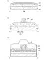
<トランジスタ150の作製工程>
図2および図3を用いて、図1に示すトランジスタ150の作製工程の一例について説明
する。<Manufacturing Process of
An example of a manufacturing process of the
まず、基板100を準備し、基板100上に下地膜102を形成する(図2(A)参照。
)。First, the
).
基板100として使用することのできる基板に大きな制限はないが、少なくとも、後の熱
処理に耐えうる程度の耐熱性を有していることが必要となる。例えば、バリウムホウケイ
酸ガラスやアルミノホウケイ酸ガラスなどのガラス基板、セラミック基板、石英基板、サ
ファイア基板などの基板を用いることができる。また、シリコンや炭化シリコンなどの単
結晶半導体基板、多結晶半導体基板、シリコンゲルマニウムなどの化合物半導体基板、S
OI基板などを適用することも可能である。There is no particular limitation on a substrate that can be used as the
It is also possible to apply an OI substrate or the like.
また、基板100として、可撓性基板を用いてもよい。可撓性基板を用いる場合、可撓性
基板上に酸化物半導体膜106を含むトランジスタを直接作製してもよいし、他の作製基
板に酸化物半導体膜106を含むトランジスタを作製し、その後可撓性基板に剥離、転置
してもよい。なお、作製基板から可撓性基板に剥離、転置するために、作製基板と酸化物
半導体膜106を含むトランジスタとの間に剥離層を設けるとよい。Further, a flexible substrate may be used as the
なお、基板100は、下地膜102を成膜する前に表面に吸着する不純物(例えば、水素
、水分または有機物など。)を低減する処理を行うことが好ましい。基板表面が十分に清
浄である場合、基板表面に吸着する不純物を低減する処理を行わなくても構わない。Note that the
基板表面に吸着する不純物を低減する方法として、例えばプラズマ処理、加熱処理または
薬液処理を行えばよい。好ましくはプラズマ処理を行う。プラズマ処理は、具体的には希
ガス(ヘリウム、ネオン、アルゴン、クリプトン、キセノンなど)、酸素または窒素を含
む雰囲気においてプラズマを生成し、基板に対してバイアス電圧を印加することで基板表
面の処理を行えばよい。なお、当該処理を行った後、大気暴露せずに下地膜102を成膜
することで、大気暴露による基板100表面への不純物の再吸着を防止することができる
ため好ましい。As a method for reducing impurities adsorbed on the substrate surface, for example, plasma treatment, heat treatment, or chemical treatment may be performed. Preferably, plasma treatment is performed. Specifically, plasma processing generates plasma in an atmosphere containing a rare gas (such as helium, neon, argon, krypton, or xenon), oxygen, or nitrogen, and applies a bias voltage to the substrate to treat the substrate surface. Can be done. Note that it is preferable that the
また、基板100は、予め基板100の歪み点より低い温度で加熱処理を行い、基板10
0をシュリンク(熱収縮とも言われる。)させておくことが好ましい。これにより、トラ
ンジスタ150の作製工程での基板加熱により生じるシュリンクの量を抑えることができ
るため、例えば、露光工程などでのマスクずれを抑制することができる。In addition, the
It is preferable to shrink 0 (also referred to as heat shrinkage). Accordingly, the amount of shrink caused by substrate heating in the manufacturing process of the
下地膜102としては、上述の「半導体装置の構成例」にて記載したように、インジウム
(In)および亜鉛(Zn)を含み、それらに加えてジルコニウム(Zr)、イットリウ
ム(Y)およびセリウム(Ce)から選ばれた一種又は複数種が含まれた膜を、スパッタ
リング法などにより成膜すればよい。当該膜は、後の工程にて成膜する酸化物半導体膜1
06の種結晶となりうる結晶性を有している。実施例1にて、上述条件を満たす下地膜1
02の結晶構造について、成膜条件と共に記載する。The
It has crystallinity that can be a seed crystal of 06. In Example 1, the
The crystal structure of 02 is described together with the film formation conditions.
また、上述の下地膜102は、酸化物半導体膜106の構成元素を含むため、酸化物半導
体膜106との格子不整合が小さい。そのため下地膜102と酸化物半導体膜106との
界面における界面準位密度を低減することができる。Further, since the
また、下地膜102は、酸化物絶縁膜を用いることが好ましい。このような下地膜102
を用いることにより、後の工程にて酸化物半導体膜106を形成した後、下地膜102を
加熱することにより酸素を放出することができるので、下地膜102中の過剰酸素を酸化
物半導体膜106に供給することができる。特に、下地膜102中(バルク中)に少なく
とも化学量論比を超える量の酸素が存在することが好ましい。酸化物半導体膜中の酸素欠
損は一部がキャリアの発生源となるため、トランジスタのしきい値電圧を変動させる要因
となりうるが、酸化物半導体膜106の酸素欠損を下地膜102から供給される酸素で補
填することにより、当該酸化物半導体膜を用いたトランジスタ150の電気的特性を良好
にすることができる。上述のように、下地膜102を、少なくとも化学量論比を超える量
の酸素が存在する絶縁膜とするためには、スパッタリング法を用いて下地膜102を成膜
することが好ましい。The
Since oxygen can be released by heating the
なお、上述の「加熱処理により酸素を放出する」とは、TDS(Thermal Des
orption Spectroscopy:昇温脱離ガス分光法)にて、酸素分子の放
出量が1.0×10¹⁸分子/cm3以上、好ましくは3.0×1019分子/cm3以
上、さらに好ましくは1.0×10²⁰分子/cm3以上であることをいう。Note that the above-mentioned “release oxygen by heat treatment” means TDS (Thermal Des.
The amount of released oxygen molecules is 1.0 × 10¹⁸ molecules / cm3 or more, preferably 3.0 × 10¹⁹ molecules / cm3 or more, more preferably 1 0.0 × 10²⁰ molecules / cm3 or more.
化学量論比を超える量の酸素が存在する下地膜102を形成する他の方法としては、例え
ば、下地膜102を成膜した基板を加熱装置(例えば、GRTA(Gas Rapid
Thermal Anneal)装置、LRTA(Lamp Rapid Therma
l Anneal)装置等のRTA(Rapid Thermal Anneal)装置
を用いることができる。)に投入し、高純度の酸素ガス、高純度の一酸化二窒素ガス、高
純度の亜酸化窒素ガス、又は超乾燥エア(CRDS(キャビティリングダウンレーザー分
光法)方式の露点計を用いて測定した場合の水分量が20ppm(露点換算で−55℃)
以下、好ましくは1ppm以下、より好ましくは10ppb以下の空気)を導入して加熱
処理を行う方法がある。なお、酸素ガスまたは一酸化二窒素ガスに、水、水素などが含ま
れないことが好ましい。または、熱処理装置に導入する酸素ガスまたは一酸化二窒素ガス
の純度を、6N以上好ましくは7N以上(即ち、酸素ガスまたは一酸化二窒素ガス中の不
純物濃度を1ppm以下、好ましくは0.1ppm以下)とすることが好ましい。なお、
上述の加熱処理の際に装置内の圧力を高圧状態とすることにより、下地膜102中に酸素
を効率的に添加することができる。As another method for forming the
Thermal Anneal), LRTA (Lamp Rapid Therma)
RTA (Rapid Thermal Anneal) apparatus such as l Annealing apparatus can be used. ) And measured using high-purity oxygen gas, high-purity dinitrogen monoxide gas, high-purity nitrous oxide gas, or ultra-dry air (CRDS (cavity ring-down laser spectroscopy) type dew point meter) When the water content is 20ppm (-55 ° C in terms of dew point)
In the following, there is a method of performing heat treatment by introducing air (preferably 1 ppm or less, more preferably 10 ppb or less). Note that it is preferable that water, hydrogen, and the like be not contained in the oxygen gas or the dinitrogen monoxide gas. Alternatively, the purity of the oxygen gas or nitrous oxide introduced into the heat treatment apparatus is 6N or more, preferably 7N or more (that is, the impurity concentration in the oxygen gas or nitrous oxide is 1 ppm or less, preferably 0.1 ppm or less. ) Is preferable. In addition,
Oxygen can be efficiently added to the
化学量論比を超える量の酸素が存在する下地膜102を形成する他の方法としては、例え
ば、イオン注入法、イオンドーピング法、プラズマイマージョンイオンインプランテーシ
ョン法、プラズマ処理などを用いて、下地膜102に酸素(少なくとも、酸素ラジカル、
酸素原子、酸素イオン、のいずれかを含む)を添加する方法がある。As another method for forming the
Or an oxygen atom or an oxygen ion).
また、下地膜102の表面は高い平坦性を有することが好ましい。具体的には、下地膜1
02表面の平均面粗さ(Ra)が1nm以下、好ましくは0.3nm以下、さらに好まし
くは0.1nm以下とすることが望ましい。下地膜102の表面平坦性を高くする方法と
しては、例えば、化学機械研磨(CMP:Chemical Mechanical P
olishing)処理などの平坦化処理を行えばよい。下地膜102の表面平坦性を高
めることにより、下地膜102と酸化物半導体膜106との界面状態が良好となるため、
トランジスタ150の電気的特性の変動を低減することができる。The surface of the
The average surface roughness (Ra) of 02 surface is 1 nm or less, preferably 0.3 nm or less, more preferably 0.1 nm or less. As a method for increasing the surface flatness of the
or the like) may be performed. By increasing the surface flatness of the
Variation in electrical characteristics of the
なお、下地膜102を、上述の「半導体装置の構成例」にて記載したように積層構造とし
てもよい。これにより、基板100から不純物(例えば、アルミニウム、マグネシウム、
ストロンチウムおよびボロンなどの金属元素や、水素、水など。)の酸化物半導体膜への
拡散防止効果が更に高まるため、トランジスタの電気的特性の劣化(例えば、トランジス
タのノーマリーオン化(しきい値電圧の負へのシフト)、しきい値電圧のバラツキの発生
、電界効果移動度の低下など。)を防止する効果が更に高まる。Note that the
Metal elements such as strontium and boron, hydrogen, water, etc. ) Is further enhanced in the diffusion of the oxide semiconductor film, so that the electrical characteristics of the transistor are deteriorated (for example, the transistor is normally turned on (the threshold voltage is shifted to negative), and the threshold voltage varies). , Generation of field effect mobility, etc.) is further enhanced.
また、後の工程にて下地膜102上に酸化物半導体膜106を成膜する際に、酸化物半導
体膜106が水素、又は水をなるべく含まないようにするために、酸化物半導体膜106
の成膜工程の前処理として、スパッタリング装置の予備加熱室で下地膜102が成膜され
た基板を予備加熱し、基板100及び下地膜102に吸着した水素、水分などの不純物を
脱離し排気することが好ましい。ここで、熱処理は、例えば、100℃以上450℃以下
で行えばよい。また、処理室の排気は、ドライポンプなどの粗引きポンプと、スパッタイ
オンポンプ、ターボ分子ポンプおよびクライオポンプなどの高真空ポンプとを適宜組み合
わせて行うとよい。ターボ分子ポンプは大きいサイズの分子の排気が優れる一方、水分や
水素の排気能力が低い。さらに、水分の排気能力の高いクライオポンプまたは水素の排気
能力の高いスパッタイオンポンプを組み合わせることが有効となる。また、このとき、不
活性ガスを導入しながら不純物の除去を行うと、排気するだけでは脱離しにくい水分など
の脱離速度をさらに大きくすることができる。In order to prevent the
As a pretreatment for the film formation step, the substrate on which the
なお、酸化物半導体膜106を成膜する前に、アルゴンガスを導入してプラズマを発生さ
せ、下地膜102の表面に付着している粉状物質(パーティクル、ごみともいう)や有機
物を除去する処理(逆スパッタ処理とも言われる。)を行うことが好ましい。なお、アル
ゴンに代えて、窒素、ヘリウム、酸素などのガスを用いてもよい。Note that before the
次に、下地膜102上に、スパッタリング法により酸化物半導体膜106を成膜する(図
2(B)参照)。酸化物半導体膜106の膜厚は、1nm以上200nm以下、好ましく
は1nm以上30nm以下、より好ましくは1nm以上10nm以下とすることが望まし
い。酸化物半導体膜106の膜厚を上述の膜厚とすることにより、トランジスタ150の
短チャネル効果を抑制することができる。なお、下地膜102および酸化物半導体膜10
6は、大気に触れさせることなく連続して成膜することが好ましい。Next, the
6 is preferably formed continuously without exposure to the atmosphere.
なお、本実施の形態では、In−Ga−Zn系酸化物ターゲットを用いてスパッタリング
法により酸化物半導体膜106を成膜する。また、酸化物半導体膜106は、希ガス(代
表的にはアルゴン)雰囲気下、酸素雰囲気下、又は希ガスと酸素の混合雰囲気下において
スパッタリング法により形成することができる。Note that in this embodiment, the
酸化物半導体膜106としてIn−Ga−Zn−O膜をスパッタリング法で作製するため
のターゲットとしては、例えば、原子数比がIn:Ga:Zn=1:1:1の酸化物ター
ゲットや、原子数比がIn:Ga:Zn=3:1:2の酸化物ターゲットや、原子数比が
In:Ga:Zn=2:1:3の酸化物ターゲットや、原子数比がIn:Ga:Zn=1
:3:2の酸化物ターゲットを用いることができる。ただし、酸化物半導体膜106のタ
ーゲットは、これらのターゲットの材料及び組成に限定されるものではない。As a target for forming an In—Ga—Zn—O film as the
An oxide target of 3: 3 can be used. Note that the target of the
また、酸化物ターゲットの相対密度は90%以上100%以下、好ましくは95%以上9
9.9%以下である。相対密度の高い酸化物ターゲットを用いることにより、成膜した酸
化物半導体膜106は緻密な膜とすることができる。The relative density of the oxide target is 90% to 100%, preferably 95% to 9%.
It is 9.9% or less. By using an oxide target with high relative density, the formed
酸化物半導体膜106を成膜する際に用いるスパッタガスとしては、水素、水、水酸基又
は水素化物などの不純物が除去された高純度ガスを用いることが好ましい。As a sputtering gas used for forming the
酸化物半導体膜106に、水素が多量に含まれると、酸化物半導体と結合することによっ
て、水素の一部がドナーとなり、キャリアである電子を生じてしまう。これにより、トラ
ンジスタのしきい値電圧がマイナス方向にシフトしてしまう。そのため、酸化物半導体膜
106において、水素濃度は、5×10¹⁸atoms/cm3未満、好ましくは1×1
018atoms/cm3以下、より好ましくは5×1017atoms/cm3以下、
更に好ましくは1×10¹⁶atoms/cm3以下とすることが望ましい。なお、上述
の酸化物半導体膜中の水素濃度は、二次イオン質量分析法(SIMS:Secondar
y Ion Mass Spectrometry)で測定されるものである。When the
018 atoms / cm3 or less, more preferably 5 × 10¹⁷ atoms / cm3 or less,
More preferably, it is 1 × 10¹⁶ atoms / cm3 or less. Note that the hydrogen concentration in the oxide semiconductor film is determined by secondary ion mass spectrometry (SIMS).
(y Ion Mass Spectrometry).
例えば、純度が6N以上好ましくは7N以上(即ち、ガス中の不純物濃度を1ppm以下
、好ましくは0.1ppm以下)の成膜ガスを用いることが望ましい。For example, it is desirable to use a deposition gas having a purity of 6N or more, preferably 7N or more (that is, the impurity concentration in the gas is 1 ppm or less, preferably 0.1 ppm or less).
また、成膜室内の水分(水、水蒸気、水素、水酸基または水酸化物を含む)を除去するた
めに、吸着型の真空ポンプ、例えば、クライオポンプ、イオンポンプ、チタンサブリメー
ションポンプを用いることが好ましい。また、排気手段は、ターボ分子ポンプにコールド
トラップを加えたものであってもよい。クライオポンプを用いて排気した成膜室は、例え
ば、水素原子、水(H2O)など水素原子を含む化合物(より好ましくは炭素原子を含む
化合物も)等が排気されるため、当該成膜室で成膜した酸化物半導体膜に含まれる水素、
水分などの不純物の濃度を低減できる。In order to remove moisture (including water, water vapor, hydrogen, hydroxyl group, or hydroxide) in the deposition chamber, an adsorption-type vacuum pump such as a cryopump, an ion pump, or a titanium sublimation pump is used. preferable. The exhaust means may be a turbo molecular pump provided with a cold trap. In the film formation chamber evacuated using a cryopump, for example, a compound containing a hydrogen atom (more preferably a compound containing a carbon atom) such as a hydrogen atom or water (H2 O) is exhausted. Hydrogen contained in the oxide semiconductor film formed in the chamber,
The concentration of impurities such as moisture can be reduced.
加えて、酸化物半導体膜には窒素も極力含まれていないことが好ましい。これは、水素の
場合と同様に、酸化物半導体と結合することによって、窒素の一部がドナーとなり、キャ
リアである電子を生じてしまうためである。そのため、酸化物半導体膜を加熱してTDS
測定を行った場合において、当該膜からのアンモニア分子の放出量のピークが5.0×1
021分子/cm3以下、好ましくは1.0×1021分子/cm3以下、より好ましく
は8.0×10²¹分子/cm3以下である膜を用いることが望ましい。In addition, the oxide semiconductor film preferably contains as little nitrogen as possible. This is because, as in the case of hydrogen, by bonding with an oxide semiconductor, part of nitrogen becomes a donor and an electron which is a carrier is generated. Therefore, by heating the oxide semiconductor film, TDS
When the measurement is performed, the peak of the amount of released ammonia molecules from the film is 5.0 × 1.
It is desirable to use a film having 021 molecules / cm3 or less, preferably 1.0 × 10²¹ molecules / cm3 or less, more preferably 8.0 × 10²¹ molecules / cm3 or less.
なお、酸化物半導体膜106に、アルカリ金属またはアルカリ土類金属が含まれると、酸
化物半導体と結合することによって、キャリアが生成されることがあり、トランジスタの
オフ電流が上昇する原因となる。そのため、酸化物半導体膜106において、アルカリ金
属またはアルカリ土類金属の濃度は、1×10¹⁸atoms/cm3以下、好ましくは
2×10¹⁶atoms/cm3以下とすることが望ましい。Note that in the case where the
酸化物半導体膜106としてCAAC−OS膜を適用する場合、当該CAAC−OS膜を
形成する方法として二つの方法が挙げられる。一つめは、成膜温度を200℃以上450
℃以下として酸化物半導体膜の成膜を行うことで、酸化物半導体膜の被形成面または表面
の法線ベクトルに対してc軸が平行な方向に揃った結晶部を形成する方法である。二つめ
は、酸化物半導体膜を薄い膜厚で成膜した後、200℃以上700℃以下の熱処理を行う
ことで、酸化物半導体膜の被形成面または表面の法線ベクトルに対してc軸が平行な方向
に揃った結晶部を形成する方法である。In the case where a CAAC-OS film is used as the
In this method, an oxide semiconductor film is formed at a temperature equal to or lower than 0 ° C. to form a crystal part in which the c-axis is aligned in a direction parallel to the normal vector of the surface or surface of the oxide semiconductor film. Second, after forming the oxide semiconductor film with a small thickness, heat treatment is performed at 200 ° C. or more and 700 ° C. or less, so that the c-axis with respect to the normal vector of the surface or surface of the oxide semiconductor film is formed. Is a method of forming crystal parts aligned in parallel directions.
酸化物半導体膜106は、下地(本実施の形態では、下地膜102が下地に相当する。)
の結晶性を反映して成膜されるため、例えば、酸化シリコンなどの非晶質な膜が用いられ
ている場合、酸化物半導体膜106は下地膜102との界面近傍において非晶質状態とな
りやすい。The
For example, when an amorphous film such as silicon oxide is used, the
これに対し、本明細書の一態様に記載するように、下地膜102として結晶性を有する酸
化物膜を用いる場合、酸化物半導体膜106と下地膜102の格子不整合が小さいため、
酸化物半導体膜106は下地膜102の結晶状態を反映して(下地膜102を種結晶とし
て、とも表現できる。)下地膜102との界面近傍から結晶成長をする。したがって、酸
化物半導体膜106を、下地膜102との界面近傍から膜厚方向の広い範囲において結晶
性を有するCAAC−OS膜とすることができる。On the other hand, as described in one embodiment of the present specification, when an oxide film having crystallinity is used as the
The
なお、スパッタリング法を用いて酸化物半導体膜106を成膜する際に、酸化物半導体膜
106を構成する元素などが高いエネルギーを持って下地膜102に衝突すると、下地膜
102を構成する元素の結合が切れ、その結合の切れた元素が酸化物半導体膜106中に
混入してしまう(ミキシング現象、ミキシング効果とも言われる。)。特に、下地膜10
2との界面近傍の酸化物半導体膜106において、当該現象は顕著に生じる。Note that when the
The phenomenon occurs remarkably in the
下地膜102として、絶縁膜として一般的に用いられている膜、例えば酸化シリコンなど
の非晶質な膜を用いた場合、上述のようなミキシング現象が生じた場合、酸化物半導体膜
の結晶化を阻害する元素であるシリコンなどの不純物が、酸化物半導体膜中、特に酸化シ
リコンとの界面近傍の酸化物半導体膜中に取り込まれて酸化物半導体膜の一部が非晶質状
態となるため、トランジスタの電気的特性(例えば、オフ電流やしきい値電圧バラツキな
ど。)に悪影響を及ぼす。これに対し、本明細書の一態様に記載のとおり、酸化物半導体
膜の構成元素を含む結晶性を有する酸化物膜を下地膜102として用いた場合、下地膜1
02は酸化物半導体膜の結晶化を阻害する元素が含まれない、または、結晶化を阻害する
だけの濃度で含まれないため、仮に上述のようなミキシングが生じた場合においても、下
地膜102からの不純物(結晶化を阻害する元素、とも言える。)の混入による酸化物半
導体膜106の結晶性の低下を抑制することができるため、トランジスタの電気的特性の
変動を抑制できる。In the case where a film generally used as an insulating film, for example, an amorphous film such as silicon oxide, is used as the
02 does not include an element that inhibits crystallization of the oxide semiconductor film, or does not include a concentration that inhibits crystallization. Therefore, even when the above-described mixing occurs, the
なお、基板100を加熱しながら成膜することにより、成膜した酸化物半導体膜106に
含まれる水素や水などの不純物濃度を低減する(脱水化処理、脱水素化処理とも表現でき
る。)ことができる。また、スパッタリングによる損傷が軽減されるため好ましい。Note that by performing deposition while the
なお、酸化物半導体膜106として、CAAC−OS膜以外の結晶性を有する酸化物半導
体膜(単結晶または多結晶)を成膜する場合には、成膜温度は特に限定されない。CAA
C−OS膜以外の結晶性を有する酸化物半導体膜を成膜する場合においても、下地膜10
2として結晶性を有する酸化物膜を用いることにより、下地膜102の結晶状態を反映し
て下地膜102との界面近傍から結晶成長をするため、酸化物半導体膜106を、下地膜
102との界面近傍から膜厚方向の広い範囲において結晶性を有する膜とすることができ
る。Note that in the case where an oxide semiconductor film (single crystal or polycrystal) having crystallinity other than the CAAC-OS film is formed as the
In the case where an oxide semiconductor film having crystallinity other than the C-OS film is formed, the base film 10
By using an oxide film having crystallinity as 2 to reflect the crystal state of the
酸化物半導体膜106の成膜後、酸化物半導体膜106に対して、熱処理を行ってもよい
。当該熱処理の温度は、300℃以上700℃以下、または基板の歪み点未満とする。当
該熱処理を行うことで、過剰な水素(水や水酸基を含む)を除去することが可能である。After the
当該熱処理は、例えば、抵抗発熱体などを用いた電気炉に被処理物を導入し、窒素雰囲気
下、450℃、1時間の条件で行うことができる。この間、酸化物半導体膜106は大気
に触れさせず、水や水素の混入が生じないようにする。The heat treatment can be performed, for example, by introducing an object to be processed into an electric furnace using a resistance heating element and the like under a nitrogen atmosphere at 450 ° C. for one hour. During this time, the
熱処理装置は電気炉に限られず、加熱されたガスなどの媒体からの熱伝導、または熱輻射
によって、被処理物を加熱する装置を用いても良い。例えば、GRTA(Gas Rap
id Thermal Anneal)装置、LRTA(Lamp Rapid The
rmal Anneal)装置等のRTA(Rapid Thermal Anneal
)装置を用いることができる。LRTA装置は、ハロゲンランプ、メタルハライドランプ
、キセノンアークランプ、カーボンアークランプ、高圧ナトリウムランプ、高圧水銀ラン
プなどのランプから発する光(電磁波)の輻射により、被処理物を加熱する装置である。
GRTA装置は、高温のガスを用いて熱処理を行う装置である。ガスとしては、アルゴン
などの希ガス、または窒素のような、熱処理によって被処理物と反応しない不活性気体が
用いられる。The heat treatment apparatus is not limited to an electric furnace, and an apparatus for heating an object to be processed by heat conduction or heat radiation from a medium such as a heated gas may be used. For example, GRTA (Gas Rap
id Thermal Anneal) device, LRTA (Lamp Rapid The
RTA (Rapid Thermal Anneal) equipment, etc.
) Device can be used. The LRTA apparatus is an apparatus that heats an object to be processed by radiation of light (electromagnetic waves) emitted from a lamp such as a halogen lamp, a metal halide lamp, a xenon arc lamp, a carbon arc lamp, a high pressure sodium lamp, or a high pressure mercury lamp.
The GRTA apparatus is an apparatus that performs heat treatment using a high-temperature gas. As the gas, an inert gas that does not react with an object to be processed by heat treatment, such as nitrogen or a rare gas such as argon, is used.
例えば、当該熱処理として、熱せられた不活性ガス雰囲気中に被処理物を投入し、数分間
熱した後、当該不活性ガス雰囲気から被処理物を取り出すGRTA処理を行ってもよい。
GRTA処理を用いると短時間での高温熱処理が可能となる。また、被処理物の耐熱温度
を超える温度条件であっても適用が可能となる。なお、処理中に、不活性ガスを、酸素を
含むガスに切り替えても良い。For example, as the heat treatment, a GRTA process may be performed in which an object to be processed is put in a heated inert gas atmosphere, heated for several minutes, and then the object to be processed is taken out from the inert gas atmosphere.
When GRTA treatment is used, high-temperature heat treatment can be performed in a short time. In addition, application is possible even under temperature conditions exceeding the heat resistance temperature of the object to be processed. Note that the inert gas may be switched to a gas containing oxygen during the treatment.
なお、不活性ガス雰囲気としては、窒素、または希ガス(ヘリウム、ネオン、アルゴン等
)を主成分とする雰囲気であって、水、水素などが含まれない雰囲気を適用するのが望ま
しい。例えば、熱処理装置に導入する窒素や、ヘリウム、ネオン、アルゴン等の希ガスの
純度を、6N(99.9999%)以上、好ましくは7N(99.99999%)以上(
すなわち、不純物濃度が1ppm以下、好ましくは0.1ppm以下)とする。Note that as the inert gas atmosphere, an atmosphere containing nitrogen or a rare gas (such as helium, neon, or argon) as a main component and not including water, hydrogen, or the like is preferably used. For example, the purity of nitrogen or a rare gas such as helium, neon, or argon introduced into the heat treatment apparatus is 6N (99.9999%) or more, preferably 7N (99.99999%) or more (
That is, the impurity concentration is 1 ppm or less, preferably 0.1 ppm or less.
なお、上述の脱水化又は脱水素化処理を行うと、酸化物半導体膜を構成する主成分材料で
ある酸素が同時に脱離して減少してしまうおそれがある。酸化物半導体膜において、酸素
が脱離した箇所では酸素欠損が存在し、当該酸素欠損に起因してトランジスタの電気的特
性変動を招くドナー準位が生じてしまう。よって、脱水化又は脱水素化処理を行った場合
、酸化物半導体膜106中に、酸素を供給することが好ましい。酸化物半導体膜106中
に酸素を供給することにより、膜中の酸素欠損を補填することができる。Note that when the above dehydration or dehydrogenation treatment is performed, oxygen which is a main component material of the oxide semiconductor film may be desorbed and reduced at the same time. In the oxide semiconductor film, oxygen vacancies exist at locations where oxygen is released, and donor levels that cause fluctuations in electrical characteristics of the transistor are generated due to the oxygen vacancies. Therefore, oxygen is preferably supplied into the
酸化物半導体膜106中の酸素欠損を補填する方法としては、例えば、酸化物半導体膜1
06に対して脱水化処理(脱水素化処理)を行った後、同じ炉に高純度の酸素ガス、高純
度の一酸化二窒素ガス、高純度の亜酸化窒素ガス、又は超乾燥エア(CRDS(キャビテ
ィリングダウンレーザー分光法)方式の露点計を用いて測定した場合の水分量が20pp
m(露点換算で−55℃)以下、好ましくは1ppm以下、より好ましくは10ppb以
下の空気)を導入すればよい。酸素ガスまたは一酸化二窒素ガスに、水、水素などが含ま
れないことが好ましい。または、熱処理装置に導入する酸素ガスまたは一酸化二窒素ガス
の純度を、6N以上好ましくは7N以上(即ち、酸素ガスまたは一酸化二窒素ガス中の不
純物濃度を1ppm以下、好ましくは0.1ppm以下)とすることが好ましい。なお、
上述の加熱処理の際に装置内の圧力を高圧状態とすることにより、酸化物半導体膜106
中に酸素を効率的に添加することができる。As a method for filling oxygen vacancies in the
After dehydration treatment (dehydrogenation treatment) on 06, high purity oxygen gas, high purity dinitrogen monoxide gas, high purity nitrous oxide gas, or ultra-dry air (CRDS) was applied to the same furnace. Water content when measured using a (cavity ring down laser spectroscopy) type dew point meter is 20pp
m (air at dew point conversion of −55 ° C.) or less, preferably 1 ppm or less, more preferably 10 ppb or less). It is preferable that water, hydrogen, and the like are not contained in the oxygen gas or the dinitrogen monoxide gas. Alternatively, the purity of the oxygen gas or nitrous oxide introduced into the heat treatment apparatus is 6N or more, preferably 7N or more (that is, the impurity concentration in the oxygen gas or nitrous oxide is 1 ppm or less, preferably 0.1 ppm or less. ) Is preferable. In addition,
By setting the pressure in the apparatus to a high-pressure state during the above heat treatment, the
Oxygen can be efficiently added therein.
また、酸化物半導体膜106中の酸素欠損を補填する他の方法としては、例えば、イオン
注入法、イオンドーピング法、プラズマイマージョンイオンインプランテーション法、プ
ラズマ処理などを用いて、酸化物半導体膜106に酸素(少なくとも、酸素ラジカル、酸
素原子、酸素イオン、のいずれかを含む)を添加する方法がある。As another method for filling oxygen vacancies in the
上述のように、成膜後の酸化物半導体膜106には、脱水化処理(脱水素化処理)を行い
水素もしくは水分を酸化物半導体膜から除去して不純物が極力含まれないように高純度化
し、脱水化処理(脱水素化処理)によって同時に減少してしまった酸化物半導体膜を構成
する主成分材料である酸素を供給(過酸素化とも表現できる。)して酸素欠損を補填する
ことによって、i型(真性)化またはi型に限りなく近い酸化物半導体膜106とするこ
とができる。そうすることにより、酸化物半導体膜のフェルミ準位(Ef)を真性フェル
ミ準位(Ei)と同じレベルにまですることができる。よって、当該酸化物半導体膜をト
ランジスタに用いることで、酸素欠損に起因するトランジスタのしきい値電圧Vthのば
らつき等を低減することができる。As described above, the
なお、酸化物半導体膜106の脱水化処理(脱水素化処理)は、酸化物半導体膜106へ
の酸素の供給工程の前に行っておくことが好ましい。Note that the dehydration treatment (dehydrogenation treatment) of the
なお、上述では、酸化物半導体膜106を島状に加工する前に脱水素化処理、過酸化処理
を行う構成について説明したが、開示する発明の一態様はこれに限定して解釈されない。
酸化物半導体膜106を島状に加工した後に、当該処理を行ってもよい。Note that although the structure in which the dehydrogenation treatment and the peroxidation treatment are performed before the
The treatment may be performed after the
次に、酸化物半導体膜106をフォトリソグラフィ工程により島状の酸化物半導体膜10
6に加工する(図2(C)参照。)。また、島状の酸化物半導体膜106を形成するため
のレジストマスクをインクジェット法で形成してもよい。レジストマスクをインクジェッ
ト法で形成するとフォトマスクを使用しないため、製造コストを低減できる。なお、酸化
物半導体膜106のエッチングは、ドライエッチングでもウェットエッチングでもよく、
両方を用いてもよい。Next, the
6 (see FIG. 2C). Further, a resist mask for forming the island-shaped
Both may be used.
ここで、図2(C)に示すように、酸化物半導体膜106は端部に20°乃至50°のテ
ーパー角を有していることが好ましい。酸化物半導体膜106の端部にテーパー角を有す
ることで酸素欠損の発生を抑制し、トランジスタ150のリーク電流の発生を低減するこ
とができる。Here, as illustrated in FIG. 2C, the
次に、酸化物半導体膜106上に、ゲート絶縁膜108を形成するための絶縁膜107を
形成する(図2(D)参照。)。ここで、絶縁膜107の膜厚は、例えば1nm以上50
nm以下とすることができる。また、絶縁膜107の成膜方法としては、例えば、スパッ
タリング法、MBE法、CVD法、パルスレーザ堆積法、ALD法等を適宜用いることが
できる。Next, the insulating
nm or less. As a method for forming the insulating
絶縁膜107は、十分な耐圧および絶縁性を有する酸化物絶縁膜を用いることが好ましい
。
絶縁膜107としては、例えば、CVD法またはスパッタリング法等を用いて、酸化シリ
コン膜、酸化窒化シリコン膜、窒化シリコン膜、窒化酸化シリコン膜、酸化アルミニウム
膜、窒化アルミニウム膜、酸化窒化アルミニウム膜、窒化酸化アルミニウム膜、酸化ガリ
ウム膜、酸化イットリウム膜、酸化ランタン膜などを、単層でまたは積層して形成するこ
とができる。また、酸化ハフニウム膜、ハフニウムシリケート膜(HfSixOy(x>
0、y>0))、窒素が添加されたハフニウムシリケート膜(HfSiOxNy(x>0
、y>0))、ハフニウムアルミネート膜(HfAlxOy(x>0、y>0))などの
high−k材料を絶縁膜107の少なくとも一部として用いてもよい。これによりゲー
トリーク電流を低減することができる。As the insulating
As the insulating
0, y> 0)), nitrogen-added hafnium silicate film (HfSiOx Ny (x> 0
, Y> 0)), and a high-k material such as a hafnium aluminate film (HfAlx Oy (x> 0, y> 0)) may be used as at least part of the insulating
なお、絶縁膜107として酸化物絶縁膜を用いることにより、下地膜102と同様に、熱
処理によって当該酸化物絶縁膜の酸素の一部を脱離させて酸化物半導体膜106に酸素を
供給し、酸化物半導体膜106中の酸素欠損を補填することができる。当該処理の詳細に
ついては、下地膜102の説明を参酌すればよく、絶縁膜107に対する加熱処理を行う
タイミングについては、絶縁膜107の成膜後であれば特段の限定はない。Note that by using an oxide insulating film as the insulating
特に、絶縁膜107中(バルク中)に少なくとも化学量論比を超える量の酸素が存在する
ことが好ましく、例えば、絶縁膜107として、SiO2+α(ただし、α>0)で表さ
れる酸化シリコン膜を用いることが好ましい。このような酸化シリコン膜を絶縁膜107
として用いることで、酸化物半導体膜106に酸素を供給することができ、当該酸化物半
導体膜106を用いたトランジスタ150のトランジスタ特性を良好にすることができる
。In particular, it is preferable that oxygen in an amount exceeding at least the stoichiometric ratio is present in the insulating film 107 (in the bulk). For example, the insulating
As a result, oxygen can be supplied to the
このため、絶縁膜107を積層構造とする場合、酸化シリコン膜の上に、酸化ガリウム膜
、酸化アルミニウム膜、酸化窒化アルミニウム膜、窒化酸化アルミニウム膜、窒化シリコ
ン膜、酸化窒化シリコン膜、窒化酸化シリコン膜、酸化イットリウム膜または酸化ランタ
ン膜などを積層することが好ましい。また、酸化シリコン膜の上に、酸化ハフニウム膜、
ハフニウムシリケート膜(HfSixOy(x>0、y>0))、窒素が添加されたハフ
ニウムシリケート膜(HfSiOxNy(x>0、y>0))、ハフニウムアルミネート
膜(HfAlxOy(x>0、y>0))などのhigh−k材料を積層してもよい。こ
れらのhigh−k材料を絶縁膜107の少なくとも一部として用いることでゲートリー
ク電流を低減することができる。Therefore, when the insulating
Hafnium silicate film (HfSix Oy (x> 0, y> 0)), nitrogen-added hafnium silicate film (HfSiOx Ny (x> 0, y> 0)), hafnium aluminate film (HfAlx A high-k material such as Oy (x> 0, y> 0)) may be stacked. By using these high-k materials as at least part of the insulating
絶縁膜107として酸化物絶縁膜を用いることにより、当該酸化物絶縁膜を加熱すること
により酸素を放出させることができるので、酸化物半導体膜106に酸素を供給し、酸化
物半導体膜106中の酸素欠損を補填することができる。特に、絶縁膜107中(バルク
中)に少なくとも化学量論比を超える量の酸素が存在することが好ましく、例えば、絶縁
膜107として、SiO2+α(ただし、α>0)で表される酸化シリコン膜を用いるこ
とが好ましい。このような酸化シリコン膜を絶縁膜107として用いることで、酸化物半
導体膜106に酸素を供給することができ、当該酸化物半導体膜106を用いたトランジ
スタ150のトランジスタ特性を良好にすることができる。By using an oxide insulating film as the insulating
絶縁膜107を、少なくとも化学量論比を超える量の酸素が存在する絶縁膜とするために
は、スパッタリング法を用いて絶縁膜107を成膜することが好ましい。また、スパッタ
リング法を用いた場合、上述のように高純度のガスを使用する、成膜装置をベークして排
気装置で不純物を排気する、および基板を予備加熱するなどの方法で成膜装置内の水素や
水分などの不純物を極力除去することにより、絶縁膜107中の水素や水分の濃度を低く
抑えることが可能であり、このような観点から考えても、絶縁膜107の成膜はスパッタ
リング法を用いることが好ましいと言える。In order to make the insulating
次に、絶縁膜107上に、ゲート電極110(これと同じ層で形成される配線を含む)を
形成するための導電膜109を形成する(図3(A)参照。)。導電膜109としては、
例えば、モリブデン、チタン、タンタル、タングステン、アルミニウム、銅、ネオジム、
スカンジウム等の金属材料又はこれらを主成分とする合金材料を用いることができる。ゲ
ート電極に用いる導電膜としては、導電性の金属酸化物を用いて形成しても良い。導電性
の金属酸化物としては酸化インジウム(In2O3)、酸化スズ(SnO2)、酸化亜鉛
(ZnO)、インジウムスズ酸化物(In2O3−SnO2、ITOと略記する場合があ
る)、インジウム亜鉛酸化物(In2O3−ZnO)、または、これらの金属酸化物材料
にシリコン若しくは酸化シリコンを含有させたものを用いることができる。ゲート電極は
、上記の材料を用いて単層で又は積層して形成することができる。形成方法も特に限定さ
れず、蒸着法、CVD法、スパッタリング法、スピンコート法などの各種成膜方法を用い
ることができる。Next, a
For example, molybdenum, titanium, tantalum, tungsten, aluminum, copper, neodymium,
A metal material such as scandium or an alloy material containing these as a main component can be used. The conductive film used for the gate electrode may be formed using a conductive metal oxide. The conductive metal oxide may be abbreviated as indium oxide (In2 O3 ), tin oxide (SnO2 ), zinc oxide (ZnO), indium tin oxide (In2 O3 —SnO2 , ITO). ), Indium zinc oxide (In2 O3 —ZnO), or a metal oxide material containing silicon or silicon oxide can be used. The gate electrode can be formed using a single layer or stacked layers using the above materials. There is no particular limitation on the formation method, and various film formation methods such as an evaporation method, a CVD method, a sputtering method, and a spin coating method can be used.
また、絶縁膜107と接する導電膜109の一層として、窒素を含む金属酸化物膜、具体
的には、窒素を含むIn−Ga−Zn−O膜や、窒素を含むIn−Sn−O膜や、窒素を
含むIn−Ga−O膜や、窒素を含むIn−Zn−O膜や、窒素を含むSn−O膜や、窒
素を含むIn−O膜や、金属窒化膜(InN、SnNなど)を用いることができる。これ
らの膜は5eV(電子ボルト)、好ましくは5.5eV(電子ボルト)以上の仕事関数を
有し、当該膜を導電膜109として用いた場合、トランジスタの電気的特性のしきい値電
圧をプラスにすることができ、所謂ノーマリーオフのスイッチング素子を実現できる。Further, as one layer of the
次に、フォトリソグラフィ工程により導電膜109上にレジストマスクを形成し、選択的
にエッチングを行って、ゲート電極110およびゲート絶縁膜108を形成した後、レジ
ストマスクを除去する(図3(B)参照。)。また、ゲート電極110およびゲート絶縁
膜108を形成するためのレジストマスクをインクジェット法で形成してもよい。レジス
トマスクをインクジェット法で形成するとフォトマスクを使用しないため、製造コストを
低減できる。なお、ゲート電極110およびゲート絶縁膜108のエッチングは、ドライ
エッチングでもウェットエッチングでもよく、両方を用いてもよい。Next, a resist mask is formed over the
次に、イオンドーピング法やイオン注入法により、酸化物半導体膜106の導電率を変化
させる不純物イオン130を、酸化物半導体膜106に添加する。この際、ゲート電極1
10およびゲート絶縁膜108がマスクとして機能するため、酸化物半導体膜106中に
高抵抗領域106a(チャネル形成領域として機能する。)および低抵抗領域106bが
自己整合的に形成される(図3(C)参照。)。なお、不純物イオン130としては、1
5族元素(代表的には窒素(N)、リン(P)、砒素(As)、およびアンチモン(Sb
))、ホウ素(B)、アルミニウム(Al)、アルゴン(Ar)、ヘリウム(He)、ネ
オン(Ne)、インジウム(In)、フッ素(F)、塩素(Cl)、チタン(Ti)、及
び亜鉛(Zn)のいずれかから選択される一以上を用いることができる。イオン注入法は
、必要なイオンのみを取り出す質量分離器を用いているため、対象物に対して不純物イオ
ン130のみを選択的に添加できる。このため、イオンドーピング法を用いて添加した場
合と比べて酸化物半導体膜106中への不純物(例えば水素など)の混入が少なくなるた
め好ましい。ただし、イオンドーピング法を除外するものではない。Next,
10 and the
Group 5 elements (typically nitrogen (N), phosphorus (P), arsenic (As), and antimony (Sb
)), Boron (B), aluminum (Al), argon (Ar), helium (He), neon (Ne), indium (In), fluorine (F), chlorine (Cl), titanium (Ti), and zinc One or more selected from any of (Zn) can be used. Since the ion implantation uses a mass separator that extracts only necessary ions, only the
次に、酸化物半導体膜106上に、ソース電極及びドレイン電極(これと同じ層で形成さ
れる配線を含む)に用いる導電膜を成膜する。ソース電極及びドレイン電極に用いる導電
膜としては、例えば、アルミニウム、クロム、銅、タンタル、チタン、モリブデン、タン
グステンから選ばれた元素を含む金属膜、または上述した元素を成分とする金属窒化物膜
(窒化チタン膜、窒化モリブデン膜、窒化タングステン膜)等を用いることができる。ま
た、アルミニウム、銅などの金属膜の下側又は上側の一方または双方にチタン、モリブデ
ン、タングステンなどの高融点金属膜またはそれらの金属窒化物膜(窒化チタン膜、窒化
モリブデン膜、窒化タングステン膜)を積層させた構成としても良い。また、ソース電極
及びドレイン電極に用いる導電膜は、導電性の金属酸化物で形成しても良い。導電性の金
属酸化物としては酸化インジウム(In2O3)、酸化スズ(SnO2)、酸化亜鉛(Z
nO)、インジウムスズ酸化物(In2O3−SnO2、ITOと略記する)、インジウ
ム亜鉛酸化物(In2O3−ZnO)を用いることができる。ソース電極及びドレイン電
極に用いる導電膜は、上記の材料を用いて単層で又は積層して成膜することができる。形
成方法も特に限定されず、蒸着法、CVD法、スパッタリング法、スピンコート法などの
各種成膜方法を用いることができる。Next, a conductive film used for a source electrode and a drain electrode (including a wiring formed using the same layer) is formed over the
nO), indium tin oxide (In2 O3 —SnO2 , abbreviated as ITO), and indium zinc oxide (In2 O3 —ZnO) can be used. The conductive film used for the source electrode and the drain electrode can be formed as a single layer or stacked layers using any of the above materials. There is no particular limitation on the formation method, and various film formation methods such as an evaporation method, a CVD method, a sputtering method, and a spin coating method can be used.
そして、フォトリソグラフィ工程により導電膜上にレジストマスクを形成し、選択的にエ
ッチングを行ってソース電極114a、ドレイン電極114bを形成した後、レジストマ
スクを除去することにより、トランジスタ150が形成される(図3(D)参照)。当該
フォトリソグラフィ工程におけるレジストマスク形成時の露光には、紫外線やKrFレー
ザ光やArFレーザ光を用いることが好ましい。よって、チャネル長L(図3(D)の矢
印Z部分に相当。)が25nm未満の露光を行う場合には、例えば、数nm〜数10nm
と極めて波長が短い超紫外線(Extreme Ultraviolet)を用いてフォ
トリソグラフィ工程でのレジストマスク形成時の露光を行うとよい。超紫外線による露光
は、解像度が高く焦点深度も大きい。従って、後に形成されるトランジスタのチャネル長
Lを微細化することが可能であり、回路の動作速度を高速化できる。Then, a resist mask is formed over the conductive film by a photolithography process, selective etching is performed to form the
It is preferable to perform exposure at the time of forming a resist mask in a photolithography process using extreme ultraviolet (Extreme Ultraviolet) having a very short wavelength. Exposure by extreme ultraviolet light has a high resolution and a large depth of focus. Therefore, the channel length L of a transistor to be formed later can be reduced, and the operation speed of the circuit can be increased.
なお、トランジスタ150のオン電流の低下を抑制する観点からは、酸化物半導体膜10
6のうちゲート電極110と重畳する部分の端部と、酸化物半導体膜106のうちソース
電極114aと接する部分の最もゲート電極に近い端部との隙間(図3(D)の矢印X部
分。本明細書中では、当該部分を「Loff幅」と呼称する。)および、酸化物半導体膜
106のうちゲート電極110と重畳する部分の端部と、酸化物半導体膜106のうちド
レイン電極114bと接する部分の最もゲート電極に近い端部との隙間(図3(D)の矢
印Y部分。当該部分についても、本明細書中では「Loff幅」と呼称する。)が極力小
さくなることが好ましい。なお、露光装置の性能限界以上の微細露光を行う場合において
、図3(D)のX部分およびY部分を小さくする方法としては、例えば、ソース電極11
4aの形成とドレイン電極114bの形成に、異なるフォトマスクを用いて形成すればよ
い。これにより、露光時において、ソース電極114aまたはドレイン電極114bの一
方のみがゲート電極110に極力近づく状態にアライメントを行うことができるため、L
off幅を小さくすることができる。Note that from the viewpoint of suppressing reduction in on-state current of the
6 between the end portion of the portion overlapping with the
Different photomasks may be used to form 4a and
The off width can be reduced.
また、トランジスタ150の製造時間や製造コストを低減する観点からは、フォトリソグ
ラフィ工程で用いるフォトマスク数及び工程数を削減することが好ましい。マスク数及び
工程数を削減する方法としては、例えば、透過した光が複数の強度となる露光マスクであ
る多階調マスクによって形成されたレジストマスクを用いてエッチング工程を行えばよい
。多階調マスクを用いて形成したレジストマスクは複数の膜厚を有する形状となり、エッ
チングを行うことでさらに形状を変形することができるため、異なるパターンに加工する
複数のエッチング工程に用いることができる。よって、一枚の多階調マスクによって、少
なくとも二種類以上の異なるパターンに対応するレジストマスクを形成することができる
。よって露光マスク数を削減することができ、対応するフォトリソグラフィ工程も削減で
きるため、工程の簡略化が可能となる。From the viewpoint of reducing the manufacturing time and manufacturing cost of the
なお、導電膜のエッチングの際に、酸化物半導体膜106がエッチングされ、分断するこ
とのないようエッチング条件を最適化することが望まれる。しかしながら、導電膜のみを
エッチングし、酸化物半導体膜106を全くエッチングしないという条件を得ることは難
しく、導電膜のエッチングの際に酸化物半導体膜106は一部のみがエッチングされ、例
えば、酸化物半導体膜106の膜厚の5%以上50%以下がエッチングされ、溝部(凹部
)を有する酸化物半導体膜106となることもある。Note that it is preferable that etching conditions be optimized so that the
ソース電極及びドレイン電極(これと同じ層で形成される配線を含む)に用いる導電膜と
して酸化物半導体材料を適用する場合には、導電膜をエッチングしてソース電極114a
およびドレイン電極114bを形成する際に、酸化物半導体膜106が極力エッチングさ
れないように、酸化物半導体膜106よりも十分エッチングされにくい酸化物半導体材料
を、導電膜として用いる必要がある。In the case where an oxide semiconductor material is used for a conductive film used for a source electrode and a drain electrode (including a wiring formed using the same layer), the conductive film is etched to form the
In forming the
ソース電極114a及びドレイン電極114bに酸化物半導体材料を適用した場合、酸化
物半導体膜106の材料や成膜条件によっては、ソース電極114a及びドレイン電極1
14bと、酸化物半導体膜106との界面が不明確になる場合もある。また、界面が不明
確になる場合、ソース電極114a及びドレイン電極114bと、酸化物半導体膜106
との混合領域または混合層と呼ぶことのできる箇所が形成されることもある。In the case where an oxide semiconductor material is used for the
The interface between 14b and the
A portion that can be called a mixed region or a mixed layer is sometimes formed.
なお、ソース電極114aおよびドレイン電極114bに用いる導電膜として、不純物イ
オンを導入して低抵抗化させた導電性材料、半導体材料を用いることもできる。Note that as the conductive film used for the
以上の工程により、図1(B)に示すトランジスタ150が形成される。Through the above process, the
また、トランジスタ150上に絶縁膜を設けてもよい。当該絶縁膜としては、ゲート絶縁
膜108と同じ材料および成膜方法を用いることができるため、上述のゲート絶縁膜10
8の内容を参酌することができる。なお、酸化アルミニウム膜は外部からの水分や水素な
どの不純物の侵入を抑制する効果が高いため、当該絶縁膜として酸化アルミニウム膜、ま
たは酸化アルミニウム膜を含む積層膜を形成することが望ましく、より好ましくは、膜密
度が3.2g/cm3以上、好ましくは3.6g/cm3以上の酸化アルミニウム膜を用
いることが望ましい。これにより、水分や水素などの不純物が酸化物半導体膜106に侵
入することを抑制できる。Further, an insulating film may be provided over the
8 contents can be taken into consideration. Note that since the aluminum oxide film has a high effect of suppressing entry of impurities such as moisture and hydrogen from the outside, it is desirable and more preferable to form an aluminum oxide film or a stacked film including the aluminum oxide film as the insulating film. It is desirable to use an aluminum oxide film having a film density of 3.2 g / cm3 or more, preferably 3.6 g / cm3 or more. Accordingly, entry of impurities such as moisture and hydrogen into the
また、トランジスタ150上に平坦化絶縁膜を設けても良い。スピンコート法、印刷法、
ディスペンス法またはインクジェット法などを用いて絶縁性を有する材料を塗布し、塗布
した材料に応じた硬化処理(例えば、加熱処理や光照射処理など。)を行い形成してもよ
い。なお、絶縁性を有する材料としては、例えば、アクリル樹脂、ポリイミド樹脂、ポリ
アミド樹脂、ポリアミドイミド樹脂、エポキシ樹脂等の有機樹脂を用いることができる。
また、低誘電率材料(low−k材料)、シロキサン系樹脂、PSG(リンガラス)、B
PSG(リンボロンガラス)等を用いることができる。なお、これらの材料で形成される
絶縁膜を複数積層させてもよい。なお、平坦化絶縁膜は水分などの不純物を比較的多く含
んでいる場合が多いため、上述の絶縁膜(例えば、酸化アルミニウムや酸化アルミニウム
を含む積層膜)上に形成することが好ましい。Further, a planarization insulating film may be provided over the
An insulating material may be applied using a dispensing method or an inkjet method, and a curing process (for example, a heat treatment or a light irradiation process) according to the applied material may be performed. Note that as the insulating material, for example, an organic resin such as an acrylic resin, a polyimide resin, a polyamide resin, a polyamideimide resin, or an epoxy resin can be used.
Also, low dielectric constant materials (low-k materials), siloxane resins, PSG (phosphorus glass), B
PSG (phosphorus boron glass) or the like can be used. Note that a plurality of insulating films formed using these materials may be stacked. Note that since the planarization insulating film often contains a relatively large amount of impurities such as moisture, the planarizing insulating film is preferably formed over the above-described insulating film (eg, a stacked film containing aluminum oxide or aluminum oxide).
以上のようにして、開示する発明の一態様は、酸化物半導体を用いた半導体装置において
、絶縁膜との界面近傍の酸化物半導体膜に含まれる不純物を低減することができる。これ
により、酸化物半導体膜の膜厚が非常に薄いトランジスタにおいても、高抵抗領域106
aがチャネル形成に悪影響を及ぼし、トランジスタ150のオン電流が低下する、などの
ような電気的特性の劣化を抑制することができる。よって、トランジスタ150を構成要
素として含む半導体装置の動作特性などの性能の向上を図ることができる。As described above, according to one embodiment of the disclosed invention, impurities contained in an oxide semiconductor film in the vicinity of an interface with an insulating film can be reduced in a semiconductor device including an oxide semiconductor. Accordingly, even in a transistor with a very thin oxide semiconductor film, the
It is possible to suppress deterioration in electrical characteristics such that a adversely affects channel formation and the on-state current of the
以上、本実施の形態に示す構成、方法などは、他の実施の形態に示す構成、方法などと適
宜組み合わせて用いることができる。The structures, methods, and the like described in this embodiment can be combined as appropriate with any of the structures, methods, and the like described in the other embodiments.
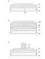
(実施の形態2)
本実施の形態では、実施の形態1とは異なる構造の半導体装置及び半導体装置の作製方法
の一形態を、図4および図5を用いて説明する。(Embodiment 2)
In this embodiment, one embodiment of a semiconductor device having a structure different from that in
<半導体装置の構成例>
図4(A)および図4(B)に、半導体装置の例として、トップゲート構造のトランジス
タの平面図および断面図の一例を示す。図4(A)は平面図であり、図4(B)は、図4
(A)におけるE−F断面の断面図である。なお、図4(A)では、煩雑になることを避
けるため、トランジスタ650の構成要素の一部(例えば、基板100など)を省略して
いる。<Configuration example of semiconductor device>
4A and 4B illustrate an example of a plan view and a cross-sectional view of a top-gate transistor as an example of a semiconductor device. 4A is a plan view and FIG. 4B is a plan view of FIG.
It is sectional drawing of the EF cross section in (A). Note that in FIG. 4A, some components (eg, the substrate 100) of the
本実施の形態のトランジスタ650は、導電膜602が下地膜102と同一平面に、下地
膜102に隣接して設けられている点で、実施の形態1に記載のトランジスタと異なって
いる。The
一般的に、活性層として酸化物半導体膜を用いたトランジスタは、導電膜との接触箇所に
おいて接触抵抗が高くなる傾向があるが、トランジスタを上述の構造とすることにより、
ソース電極114aおよびドレイン電極114bは、酸化物半導体膜106の表面側だけ
でなく、裏面側においても導電膜602を介して酸化物半導体膜106と接触するため、
酸化物半導体膜106とソース電極114aの接触抵抗および酸化物半導体膜106とド
レイン電極114bの接触抵抗を低減し、かつ接触抵抗のバラツキを低減することができ
る。これにより、オン電流が高く、かつ、しきい値電圧のバラツキを抑制された、高性能
なトランジスタとすることができるため、当該構造は酸化物半導体を用いたトランジスタ
に適した構造の1つと言える。In general, a transistor using an oxide semiconductor film as an active layer tends to have a high contact resistance at a contact portion with a conductive film.
The
The contact resistance between the
<トランジスタ650の作製工程>
図5(A)乃至図5(E)を用いて、図4に示すトランジスタ650の作製工程の一例に
ついて説明する。<Manufacturing Process of
An example of a manufacturing process of the
まず、基板100上に導電膜を成膜し、フォトリソグラフィ工程により導電膜上にレジス
トマスクを形成し、選択的にエッチングを行って、導電膜602を形成した後、レジスト
マスクを除去する(図5(A)参照。)。導電膜602に用いる材料などについては、上
述実施の形態のゲート電極110、ソース電極114a(またはドレイン電極114b)
の説明を参酌することができる。First, a conductive film is formed over the
You can refer to the explanation.
次に、基板100および導電膜602上に下地膜102を形成する(図5(B)参照。)
。ここで、下地膜102の表面は、少なくとも導電膜602の表面よりも高い位置とする
ことが好ましく、後述の平坦化処理を行うことにより、導電膜602の表面と下地膜10
2の表面を略同一とすることができる。これにより、後の工程において酸化物半導体膜1
06を成膜する際に、導電膜602と下地膜102の段差により酸化物半導体膜に断切れ
が生じるといった問題を抑制することができ、酸化物半導体膜106の膜厚を極めて薄く
することができるため、トランジスタの微細化に対し有効な手段の一つと言える。Next, the
. Here, the surface of the
The two surfaces can be substantially the same. Accordingly, the
When the layer 06 is formed, a problem that the oxide semiconductor film is cut off due to a step between the
次に、下地膜102に対して平坦化処理を施し、導電膜602の表面と略同一平面に表面
を有する下地膜102を形成する(図5(C)参照。)。なお、下地膜102の平坦化処
理は、化学的機械的研磨(Chemical Mechanical Polishin
g:CMP)処理を用いて行うことが好ましい。ここで、CMP処理とは、被加工物の表
面を基準にし、それにならって表面を化学的・機械的な複合作用により、平坦化する手法
である。一般的に研磨ステージの上に研磨布を貼り付け、被加工物と研磨布との間にスラ
リー(研磨剤)を供給しながら研磨ステージと被加工物とを各々回転または揺動させて被
加工物の表面を、スラリーと被加工物表面との間での化学反応と、研磨布と被加工物との
機械的研磨の作用により、被加工物の表面を研磨する方法である。Next, planarization treatment is performed on the
g: CMP) treatment is preferably used. Here, the CMP process is a technique for flattening the surface by a combined chemical and mechanical action based on the surface of the workpiece. In general, a polishing cloth is attached on the polishing stage, and the polishing stage and the workpiece are rotated or swung while supplying slurry (abrasive) between the workpiece and the polishing cloth. In this method, the surface of the workpiece is polished by the chemical reaction between the slurry and the workpiece surface and the mechanical polishing of the polishing cloth and the workpiece.
CMP処理は、1回行ってもよいし、複数回行ってもよい。複数回に分けてCMP処理を
行う場合は、高い研磨レートの一次研磨を行った後、低い研磨レートの仕上げ研磨を行う
のが好ましい。このように研磨レートの異なる研磨を組み合わせることによって、導電膜
602表面と下地膜102表面の平坦性をさらに向上させることができる。The CMP process may be performed once or a plurality of times. When performing the CMP process in a plurality of times, it is preferable to perform primary polishing at a low polishing rate after performing primary polishing at a high polishing rate. By combining polishing with different polishing rates in this manner, the flatness of the surface of the
また、下地膜102の平坦化処理として、ドライエッチング処理などを適用することも可
能である。エッチングガスとしては、塩素、塩化硼素、塩化珪素または四塩化炭素などの
塩素系ガス、四弗化炭素、弗化硫黄または弗化窒素などのフッ素系ガス、酸素などを適宜
用いることができる。例えば、反応性イオンエッチング(RIE:Reactive I
on Etching)法、ICP(Inductively Coupled Pla
sma)エッチング法、ECR(Electron Cyclotron Resona
nce)エッチング法、平行平板型(容量結合型)エッチング法、マグネトロンプラズマ
エッチング法、2周波プラズマエッチング法またはヘリコン波プラズマエッチング法等の
ドライエッチング法を用いることができる。特に下地膜102として窒化シリコンや窒化
酸化シリコンのような、窒素を多く含む無機絶縁材料が含まれる場合、CMP処理だけで
は窒素を多く含む無機絶縁材料の除去が困難な場合があるので、ドライエッチングなどを
併用することが好ましい。Further, a dry etching process or the like can be applied as the planarization process of the
on Etching), ICP (Inductively Coupled Pla)
sma) Etching, ECR (Electron Cyclotron Resona)
nce) A dry etching method such as an etching method, a parallel plate type (capacitive coupling type) etching method, a magnetron plasma etching method, a two-frequency plasma etching method or a helicon wave plasma etching method can be used. In particular, when the
また、下地膜102の平坦化処理として、プラズマ処理などを適用することも可能である
。プラズマ処理は、真空のチャンバーに不活性ガス、例えばアルゴンガスを導入し、被処
理面を陰極とする電界をかけて行う。その原理としてはプラズマドライエッチ法と同等で
あるが、不活性ガスを用いることで、通常のスパッタ成膜チャンバーにて処理可能であり
簡便な方法である。すなわち、このプラズマ処理は、被処理面に不活性ガスのイオンを照
射して、スパッタリング効果により表面の微細な凹凸を平坦化する処理である。このこと
から本明細書では、このプラズマ処理を「逆スパッタ」ともいう。Further, plasma treatment or the like can be applied as planarization treatment of the
なお、導電膜602および下地膜102の形状は、図5(D)のように島状に形成されて
いてもよい。また、図5(C)では導電膜602は、表面に近づくほど端部が狭まってい
る、所謂順テーパー状に形成されているが、図5(E)のように、表面に近づくほど端部
が広がっている、所謂逆テーパー状に形成してもよい。Note that the
以降の工程については、図2(A)乃至図3(D)および当該図面の説明に対応する実施
の形態1の内容を参酌して行えばよい。The subsequent steps may be performed with reference to FIGS. 2A to 3D and the contents of
以上の工程により、図4(B)に示すトランジスタ650を作製することができる。本実
施の形態では、下地膜102と重なる領域の酸化物半導体膜106は、実施の形態1と同
様に酸化物半導体膜106と下地膜102の格子不整合が小さいため、酸化物半導体膜1
06は、下地膜102の結晶状態を反映して下地膜102との界面近傍から結晶成長をす
る。したがって、酸化物半導体膜106を、下地膜102との界面近傍から膜厚方向の広
い範囲において結晶性を有するCAAC−OS膜、単結晶膜または多結晶膜とすることが
できる。Through the above steps, the
06 grows from the vicinity of the interface with the
また、トランジスタ650は、上述の特徴以外に、酸化物半導体膜106とソース電極1
14aの接触抵抗および酸化物半導体膜106とドレイン電極114bの接触抵抗を低減
し、かつ接触抵抗のバラツキを低減することができるため、オン電流が高く、かつ、しき
い値電圧のバラツキを抑制された、高性能なトランジスタとすることができる。このため
、トランジスタ650によって構成される半導体装置の動作特性の向上を図ることができ
る。そして、酸化物半導体膜を用いたトランジスタ又は該トランジスタによって構成され
る半導体装置の性能向上を図ることができる。また、上述のように、導電膜602の表面
と下地膜102の表面を略同一とすることができ、酸化物半導体膜106の膜厚を極めて
薄くすることができるため、トランジスタの微細化に適した構造の一つであると言える。In addition to the above characteristics, the
14a and the contact resistance between the
以上、本実施の形態に示す構成、方法などは、他の実施の形態に示す構成、方法などと適
宜組み合わせて用いることができる。The structures, methods, and the like described in this embodiment can be combined as appropriate with any of the structures, methods, and the like described in the other embodiments.
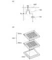
(実施の形態3)
本実施の形態では、上述の実施の形態とは異なる構造の半導体装置及び半導体装置の作製
方法の一形態を、図6乃至図8を用いて説明する。(Embodiment 3)
In this embodiment, one embodiment of a semiconductor device having a different structure from the above embodiment and a method for manufacturing the semiconductor device will be described with reference to FIGS.
<半導体装置の構成例>
図6(A)および図6(B)に、半導体装置の例として、トップゲート構造のトランジス
タの平面図および断面図の一例を示す。図6(A)は平面図であり、図6(B)は、図6
(A)におけるG−H断面の断面図である。なお、図6(A)では、煩雑になることを避
けるため、トランジスタ850の構成要素の一部(例えば、基板100など)を省略して
いる。<Configuration example of semiconductor device>
FIGS. 6A and 6B illustrate an example of a plan view and a cross-sectional view of a top-gate transistor as an example of a semiconductor device. 6A is a plan view and FIG. 6B is a plan view of FIG.
It is sectional drawing of the GH cross section in (A). Note that in FIG. 6A, some components of the transistor 850 (eg, the substrate 100) are omitted to avoid complexity.
図6(A)および図6(B)に示すトランジスタ850は、基板100上に、下地膜10
2と、酸化物半導体膜106と、絶縁膜107と、少なくとも酸化物半導体膜106と重
畳するゲート電極110と、層間絶縁膜800と、層間絶縁膜802と、絶縁膜107、
層間絶縁膜800および層間絶縁膜802の開口部を通じて酸化物半導体膜106と電気
的に接続するソース電極114aおよびドレイン電極114bを有している。A
2, the
A
トランジスタ850は、絶縁膜107が酸化物半導体膜106を覆う状態に形成されてい
る点と、ソース電極114aおよびドレイン電極114bが、絶縁膜107、層間絶縁膜
800および層間絶縁膜802の開口部を通して酸化物半導体膜106と電気的に接続し
ている点で、上述の実施の形態に記載したトランジスタの構造と異なっている。In the
トランジスタ850を、絶縁膜107が酸化物半導体膜106を覆う構造とすることによ
り、水分などの不純物が酸化物半導体膜106に侵入することを抑制できる。また、不純
物イオン130を酸化物半導体膜106に添加する際に、酸化物半導体膜106上には絶
縁膜107が存在するため、イオン添加により酸化物半導体膜106に生じるダメージ(
例えば酸化物半導体膜106中での格子欠陥の発生など)を低減することができる。When the
For example, occurrence of lattice defects in the
また、トランジスタ850を、ソース電極114aおよびドレイン電極114bが、絶縁
膜107、層間絶縁膜800および層間絶縁膜802の開口部を通して酸化物半導体膜1
06と電気的に接続している構造とすることにより、酸化物半導体膜106形成後におい
て酸化物半導体膜106がエッチング処理(例えば、ドライエッチング時のエッチングガ
スおよびプラズマや、ウェットエッチング時のエッチング剤など)に晒される箇所は、絶
縁膜107、層間絶縁膜800および層間絶縁膜802に形成される開口部のみであるた
め、当該エッチング処理により生じる物質によるトランジスタ850の汚染(例えば、ド
ライエッチング時に用いるエッチングガスが酸化物半導体膜106の金属元素と反応して
生じる金属化合物は導電性を有していることがあるため、ソース電極114aおよびドレ
イン電極114bのリークパスとなり得る可能性がある。)を抑制できる。また、ソース
電極114aおよびドレイン電極114bの一部がゲート電極110と重畳して形成され
ても、ソース電極114aとゲート電極110およびドレイン電極114bとゲート電極
110の間には層間絶縁膜が存在しており電気的に接続されることがない。これにより、
ソース電極114aおよびドレイン電極114bをゲート電極110に極力近づけて形成
することができるため、トランジスタの微細化に適した構造の一つと言える。In the
The
Since the
<トランジスタ850の作製工程>
図7(A)乃至図8(B)を用いて、図6に示すトランジスタ850の作製工程の一例に
ついて説明する。<Manufacturing Process of
An example of a manufacturing process of the
まず、基板100上に下地膜102と、酸化物半導体膜106と、絶縁膜107を形成す
る(図7(A)参照。)。なお、当該工程は、図2(A)乃至図2(D)および当該図面
の説明に対応する上述の実施の形態の内容を参酌して行えばよい。下地膜102として結
晶性を有する酸化物膜を用いることにより、実施の形態1と同様に酸化物半導体膜106
と下地膜102の格子不整合が小さいため、酸化物半導体膜106は、下地膜102の結
晶状態を反映して下地膜102との界面近傍から結晶成長をする。したがって、酸化物半
導体膜106を、下地膜102との界面近傍から膜厚方向の広い範囲において結晶性を有
するCAAC−OS膜、単結晶膜または多結晶膜とすることができる。First, the
Since the lattice mismatch between the
次に、絶縁膜107上にゲート電極110を形成し、ゲート電極110をマスクとして酸
化物半導体膜106中に不純物イオン130を添加して、酸化物半導体膜106中に低抵
抗領域106bを自己整合的に形成する(図7(B)参照。)。なお、当該工程は、図3
(A)乃至図3(C)および当該図面の説明に対応する上述の実施の形態の内容を参酌し
て行えばよい。Next, a
The contents of the above-described embodiment corresponding to (A) to FIG. 3 (C) and the description of the drawings may be referred to.
次に、絶縁膜107およびゲート電極110上に、層間絶縁膜800および層間絶縁膜8
02を形成する(図7(C)参照。)。Next, the
02 is formed (see FIG. 7C).
層間絶縁膜800としては、ゲート絶縁膜108と同じ材料および成膜方法を用いること
ができるため、上述の実施の形態にて記載したゲート絶縁膜108の内容を参酌すること
ができる。なお、酸化アルミニウム膜は外部からの水分や水素などの不純物の侵入を抑制
する効果が高いため、当該絶縁膜として酸化アルミニウム膜、または酸化アルミニウム膜
を含む積層膜を形成することが望ましく、より好ましくは、膜密度が3.2g/cm3以
上の酸化アルミニウムを用いることが望ましい。これにより、水分や水素などの不純物が
酸化物半導体膜106に侵入することを抑制できる。The
層間絶縁膜802としては、スピンコート法、印刷法、ディスペンス法またはインクジェ
ット法などを用いて絶縁性を有する材料を塗布し、塗布した材料に応じた硬化処理(例え
ば、加熱処理や光照射処理など。)を行い形成すればよい。なお、絶縁性を有する材料と
しては、例えば、アクリル樹脂、ポリイミド樹脂、ポリアミド樹脂、ポリアミドイミド樹
脂、エポキシ樹脂等の有機樹脂を用いることができる。また、低誘電率材料(low−k
材料)、シロキサン系樹脂、PSG(リンガラス)、BPSG(リンボロンガラス)等を
用いることができる。なお、これらの材料で形成される絶縁膜を複数積層させてもよい。
なお、層間絶縁膜802は水分などの不純物を比較的多く含んでいるため、上述の絶縁膜
(例えば、酸化アルミニウムや酸化アルミニウムを含む積層膜)上に形成することが好ま
しい。As the
Material), siloxane-based resin, PSG (phosphorus glass), BPSG (phosphorus boron glass) and the like can be used. Note that a plurality of insulating films formed using these materials may be stacked.
Note that since the
なお、本実施の形態では層間絶縁膜800と層間絶縁膜802の積層構造を形成したが、
いずれかの一方のみを形成してもよい。Note that a stacked structure of the
Only one of them may be formed.
次に、酸化物半導体膜と重畳する領域の絶縁膜107、層間絶縁膜800および層間絶縁
膜802の少なくとも一部に開口部を形成した後に、当該開口部を通じて酸化物半導体膜
106に電気的に接続されたソース電極114aおよびドレイン電極114bを形成する
(図8(A)参照。)。Next, after an opening is formed in at least part of the insulating
なお、絶縁膜107、層間絶縁膜800および層間絶縁膜802のエッチングは、ドライ
エッチングでもウェットエッチングでもよく、両方を用いてもよい。また、当該エッチン
グ処理の際に、酸化物半導体膜106がエッチングされ、分断することのないようエッチ
ング条件を最適化することが望まれる。しかしながら、絶縁膜107、層間絶縁膜800
および層間絶縁膜802のみをエッチングし、酸化物半導体膜106を全くエッチングし
ないという条件を得ることは難しく、導電膜のエッチングの際に酸化物半導体膜106は
一部のみがエッチングされ、例えば、酸化物半導体膜106の膜厚の5%以上50%以下
がエッチングされ、溝部(凹部)を有する酸化物半導体膜106となることもある。Note that the etching of the insulating
In addition, it is difficult to obtain a condition that only the
ソース電極114aおよびドレイン電極114bの形成工程については、図3(D)およ
び当該図面の説明に対応する上述の実施の形態の内容を参酌して行えばよい。また、当該
工程の後、ソース電極114a、ドレイン電極114bおよび層間絶縁膜802に対して
平坦化処理を行ってもよい。これにより、トランジスタ850上に更にトランジスタを積
層させて形成する場合において、被形成面(つまり、ソース電極114a、ドレイン電極
114bおよび層間絶縁膜802の表面)の平坦性が高いため、トランジスタの作製が容
易となる。なお、平坦化処理については、上述の実施の形態に記載された平坦化処理の方
法を参酌することができる。The formation process of the
以上の工程により、図6(B)に示すトランジスタ850を作製することができる。トラ
ンジスタ850は、実施の形態1にて記載した特徴以外に、上述のように、イオン添加に
より酸化物半導体膜106に生じるダメージ(例えば酸化物半導体膜106中での格子欠
陥の発生など)を低減することができる。また、上述のように、酸化物半導体膜106が
エッチング処理に晒される箇所を限定できるため、エッチング処理によるトランジスタの
汚染を抑制することができる。このため、トランジスタ850によって構成される半導体
装置の動作特性の向上を図ることができる。そして、酸化物半導体膜を用いたトランジス
タ又は該トランジスタによって構成される半導体装置の性能向上を図ることができる。ま
た、上述のように、ソース電極114aおよびドレイン電極114bの一部がゲート電極
110と重畳して形成されても電気的に接続されないため、ソース電極114aおよびド
レイン電極114bをゲート電極110に極力近づけて形成することができ、トランジス
タの微細化に適した構造の一つと言える。Through the above steps, the
また、図8(B)に示すように、導電膜602を有する構造であってもよい。トランジス
タ850を図8(B)に示す構造とすることにより、絶縁膜107、層間絶縁膜800お
よび層間絶縁膜802の一部に開口部を形成する際に、開口部の酸化物半導体膜106が
オーバーエッチングされて無くなってしまった場合においても、ソース電極114aおよ
びドレイン電極114bは、酸化物半導体膜106の側壁部分で電気的に接続される以外
に、導電膜602を介して酸化物半導体膜106と電気的に接続されるため、オーバーエ
ッチング時においても良好なコンタクト抵抗を維持することができるため、特に酸化物半
導体膜106の膜厚が薄い場合(つまり、トランジスタの微細化)に適した構造といえる
。Alternatively, a structure including a
(実施の形態4)
本実施の形態では、上述の実施の形態とは異なる構造の半導体装置及び半導体装置の作製
方法の一形態を、図9乃至図12を用いて説明する。(Embodiment 4)
In this embodiment, one embodiment of a semiconductor device having a different structure from the above embodiment and a method for manufacturing the semiconductor device will be described with reference to FIGS.
<半導体装置の構成例>
図9(A)および図9(B)に、半導体装置の例として、トップゲート構造のトランジス
タの平面図および断面図の一例を示す。図9(A)は平面図であり、図9(B)は、図9
(A)におけるI−J断面の断面図である。なお、図9(A)では、煩雑になることを避
けるため、トランジスタ1150の構成要素の一部(例えば、基板100など)を省略し
ている。<Configuration example of semiconductor device>
9A and 9B illustrate an example of a plan view and a cross-sectional view of a top-gate transistor as an example of a semiconductor device. 9A is a plan view, and FIG. 9B is a plan view of FIG.
It is sectional drawing of the IJ cross section in (A). Note that in FIG. 9A, some components of the transistor 1150 (eg, the substrate 100) are omitted to avoid complexity.
図9(A)および図9(B)に示すトランジスタ1150は、基板100上に、下地膜1
02と、酸化物半導体膜106と、ゲート絶縁膜108と、少なくとも酸化物半導体膜1
06と重畳するゲート電極110と、絶縁膜1101と、側壁絶縁膜1102と、酸化物
半導体膜106と電気的に接続するソース電極114aおよびドレイン電極114bを有
している。A
02, the
The
トランジスタ1150は、ゲート電極110上に絶縁膜1101が、ゲート電極110の
側面に側壁絶縁膜1102が設けられている点と、ソース電極114aおよびドレイン電
極114bが側壁絶縁膜1102に接して設けられている点において、上述の実施の形態
に記載したトランジスタの構造と異なっている。In the
トランジスタ1150は、後述のトランジスタ1150の作製方法でも記載するが、ソー
ス電極114aおよびドレイン電極114bとして用いる導電膜を、酸化物半導体膜10
6、絶縁膜1101および側壁絶縁膜1102上に形成した後、導電膜に対して平坦化処
理(研磨処理とも言える。)を行い導電膜の一部を除去することで、ソース電極114a
およびドレイン電極114bを形成する。そのため、ソース電極114aおよびドレイン
電極114bの形成にフォトリソグラフィ工程を用いる必要がなく、露光機の精度やフォ
トマスクのアライメントズレに影響されずにLoff幅を非常に小さくすることが可能と
なるため、トランジスタ1150のオン電流の低下を抑制することができる。また、当該
構造はトランジスタの微細化に適した構造の一つと言える。Although the
6. After the insulating
And the
<トランジスタ1150の作製工程>
図10(A)乃至図12(B)を用いて、図9に示すトランジスタ1150の作製工程の
一例について説明する。<Manufacturing Process of
An example of a manufacturing process of the
まず、基板100上に下地膜102と、酸化物半導体膜106と、絶縁膜107を形成す
る(図10(A)参照。)。なお、当該工程は、図2(A)乃至図2(D)および当該図
面の説明に対応する上述の実施の形態の内容を参酌して行えばよい。下地膜102として
結晶性を有する酸化物膜を用いることにより、実施の形態1と同様に酸化物半導体膜10
6と下地膜102の格子不整合が小さいため、酸化物半導体膜106は、下地膜102の
結晶状態を反映して下地膜102との界面近傍から結晶成長をする。したがって、酸化物
半導体膜106を、下地膜102との界面近傍から膜厚方向の広い範囲において結晶性を
有するCAAC−OS膜、単結晶膜または多結晶膜とすることができる。First, the
6 and the
次に、ゲート電極110(これと同じ層で形成される配線を含む)を形成するための導電
膜109および、絶縁膜1101を形成するための絶縁膜1100を成膜する(図10(
B)参照。)。なお、絶縁膜1100としては、ゲート絶縁膜108と同じ材料および成
膜方法を用いることができるため、上述の実施の形態にて記載したゲート絶縁膜108の
内容を参酌することができる。Next, a
See B). ). Note that the insulating
次に、フォトリソグラフィ工程により導電膜109および絶縁膜1100を島状に加工し
、ゲート電極110および絶縁膜1101を形成する(図10(C)参照。)。また、ゲ
ート電極110および絶縁膜1101を形成するためのレジストマスクをインクジェット
法で形成してもよい。レジストマスクをインクジェット法で形成するとフォトマスクを使
用しないため、製造コストを低減できる。なお、導電膜109および絶縁膜1100のエ
ッチングは、ドライエッチングでもウェットエッチングでもよく、両方を用いてもよい。Next, the
なお、本実施の形態では、導電膜109および絶縁膜1100を成膜後に両者を加工して
ゲート電極110および絶縁膜1101を形成し、その後、側壁絶縁膜1102を形成す
る順序で説明を行うため、図9(B)のように絶縁膜1101と側壁絶縁膜1102が別
の構成要素として記載されているが、絶縁膜1101と側壁絶縁膜1102は同一の膜で
あってもよい。絶縁膜1101と側壁絶縁膜1102を同一の膜とするためには、まずゲ
ート電極110を形成した後に、絶縁膜1101および側壁絶縁膜1102として機能す
る絶縁膜を、ゲート電極110を覆う状態に形成すればよい。なお、当該絶縁膜は、絶縁
膜1101および側壁絶縁膜1102の説明に記載されている材料および形成方法を参酌
することができる。Note that in this embodiment, the
次に、イオンドーピング法やイオン注入法により、酸化物半導体膜106の抵抗値を低減
する機能を有する不純物イオン130を、酸化物半導体膜106に添加する。この際、ゲ
ート電極110および絶縁膜1101がマスクとして機能するため、酸化物半導体膜10
6中に高抵抗領域106a(チャネル形成領域として機能する。)および低抵抗領域10
6bが自己整合的に形成される(図11(A)参照。)。Next,
6, a
6b is formed in a self-aligned manner (see FIG. 11A).
次に、下地膜102と同様の材料および方法で絶縁膜を成膜し、当該絶縁膜をエッチング
することにより側壁絶縁膜1102を形成する。側壁絶縁膜1102は、絶縁膜に異方性
の高いエッチング工程を行うことで自己整合的に形成することができる。例えば、ドライ
エッチング法を用いると好ましい。ドライエッチング法に用いるエッチングガスとしては
、例えば、トリフルオロメタン、オクタフルオロシクロブタン、テトラフルオロメタンな
どのフッ素を含むガスが挙げられる。エッチングガスには、希ガスまたは水素を添加して
もよい。ドライエッチング法は、基板に高周波電圧を印加する、反応性イオンエッチング
法(RIE法)を用いると好ましい。Next, an insulating film is formed using a material and a method similar to those of the
そして、側壁絶縁膜1102を形成した後、ゲート電極110、絶縁膜1101および側
壁絶縁膜1102をマスクとして絶縁膜107を加工し、ゲート絶縁膜108を形成する
ことができる(図11(B)参照。)なお、側壁絶縁膜1102の形成と同じ工程でゲー
ト絶縁膜108を形成してもよい。Then, after the
なお、本実施の形態では、ゲート電極110および絶縁膜1101の形成直後の工程にお
いて、ゲート電極110および絶縁膜1101をマスクに用いて酸化物半導体膜106中
に不純物イオン130を添加したが、側壁絶縁膜1102の形成後にゲート電極110、
絶縁膜1101および側壁絶縁膜1102をマスクに用いて、酸化物半導体膜106中に
不純物イオン130を添加してもよい。こうすることで、側壁絶縁膜1102と重畳する
酸化物半導体膜106の領域を高抵抗領域106aに含めることができる。Note that in this embodiment, the
The
次に、酸化物半導体膜106、絶縁膜1101および側壁絶縁膜1102上に、ソース電
極114aおよびドレイン電極114b(これと同じ層で形成される配線を含む)を形成
するための導電膜1104および層間絶縁膜802を成膜する(図11(C)参照。)。
なお、導電膜1104としては、例えば、アルミニウム、クロム、銅、タンタル、チタン
、モリブデン、タングステンから選ばれた元素を含む金属膜、または上述した元素を成分
とする金属窒化物膜(窒化チタン膜、窒化モリブデン膜、窒化タングステン膜)等を用い
ることができる。また、アルミニウム、銅などの金属膜の下側又は上側の一方または双方
にチタン、モリブデン、タングステンなどの高融点金属膜またはそれらの金属窒化物膜(
窒化チタン膜、窒化モリブデン膜、窒化タングステン膜)を積層させた構成としても良い
。また、ソース電極及びドレイン電極に用いる導電膜は、導電性の金属酸化物で形成して
も良い。導電性の金属酸化物としては酸化インジウム(In2O3)、酸化スズ(SnO
2)、酸化亜鉛(ZnO)、インジウムスズ酸化物(In2O3−SnO2、ITOと略
記する)、インジウム亜鉛酸化物(In2O3−ZnO)を用いることができる。ソース
電極及びドレイン電極に用いる導電膜は、上記の材料を用いて単層で又は積層して成膜す
ることができる。形成方法も特に限定されず、蒸着法、CVD法、スパッタリング法、ス
ピンコート法などの各種成膜方法を用いることができる。なお、層間絶縁膜802につい
ては、実施の形態3にて記載した層間絶縁膜802の材料や成膜方法を参酌することがで
きる。Next, the
Note that as the
A structure in which a titanium nitride film, a molybdenum nitride film, or a tungsten nitride film) is stacked may be employed. Further, the conductive film used for the source electrode and the drain electrode may be formed using a conductive metal oxide. Examples of the conductive metal oxide include indium oxide (In2 O3 ) and tin oxide (SnO
2 ), zinc oxide (ZnO), indium tin oxide (In2 O3 —SnO2 , abbreviated as ITO), and indium zinc oxide (In2 O3 —ZnO) can be used. The conductive film used for the source electrode and the drain electrode can be formed as a single layer or stacked layers using any of the above materials. There is no particular limitation on the formation method, and various film formation methods such as an evaporation method, a CVD method, a sputtering method, and a spin coating method can be used. Note that for the
次に、導電膜1104に対して上面から平坦化処理を行い、絶縁膜1101および側壁絶
縁膜1102上の少なくとも一部の導電膜1104ならびに、少なくとも一部の層間絶縁
膜802を除去することで、導電膜1104は少なくとも絶縁膜1100上または側壁絶
縁膜1102で分断され、ソース電極114aおよびドレイン電極114bがゲート電極
110を挟む状態に形成される(図12(A)参照。)。なお、ここでの平坦化処理は、
実施の形態1にて記載した下地膜102に対しての平坦化処理の内容を参酌することがで
きる。Next, planarization treatment is performed on the
The content of the planarization process for the
なお、平坦化処理は導電膜1104および層間絶縁膜802を処理(研磨)するだけでな
く、絶縁膜1101や側壁絶縁膜1102を同時に処理(研磨)してもよい。Note that in the planarization treatment, not only the
なお、図12(A)では、ソース電極114aおよびドレイン電極114bの表面と、絶
縁膜1101および層間絶縁膜802の表面が同一平面に位置しているが、CMP装置に
よりソース電極114a、ドレイン電極114bおよび絶縁膜1101を研磨する場合、
ソース電極114aおよびドレイン電極114bと、絶縁膜1101および層間絶縁膜8
02の研磨スピードが異なると、ソース電極114aおよびドレイン電極114bの表面
と、絶縁膜1101および層間絶縁膜802の表面は高さが異なり段差が生じることがあ
り、例えば、ソース電極114aおよびドレイン電極114bの表面が絶縁膜1101の
表面より低くなる(凹状となる)場合がある。Note that in FIG. 12A, the surfaces of the
When the polishing speed of 02 is different, the surface of the
以上の工程により、図9(B)に示すトランジスタ1150を作製することができる。ト
ランジスタ1150は、実施の形態1にて記載した特徴以外に、上述のように、トランジ
スタのオン電流の低下を抑制することができる。よって、トランジスタ1150によって
構成される半導体装置の動作特性の向上を図ることができる。そして、酸化物半導体膜を
用いたトランジスタ又は該トランジスタによって構成される半導体装置の性能向上を図る
ことができる。また、ソース電極114aおよびドレイン電極114bの形成にフォトリ
ソグラフィ工程を用いる必要がなく、露光機の精度やフォトマスクのアライメントズレに
影響されずにLoff幅を非常に小さくすることが可能であり、トランジスタの微細化に
適した構造の一つといえる。Through the above steps, the
また、トランジスタ1150上に絶縁膜を設けてもよい。当該絶縁膜としては、ゲート絶
縁膜108と同じ材料および成膜方法を用いることができるため、上述のゲート絶縁膜1
08の内容を参酌することができる。なお、酸化アルミニウム膜は外部からの水分の侵入
を抑制する効果が高いため、当該絶縁膜として酸化アルミニウム膜、または酸化アルミニ
ウム膜を含む積層膜を形成することが望ましく、より好ましくは、膜密度が3.2g/c
m3以上、好ましくは3.6g/cm3以上の酸化アルミニウム膜を用いることが望まし
い。なお、当該絶縁膜は、トランジスタ1150の形成前に成膜してもよい。例えば、側
壁絶縁膜1102を形成した後に、導電膜1104、当該絶縁膜、層間絶縁膜802の順
に成膜を行い、その後にCMP処理などの平坦化処理を行ってもよい。図9(B)の構造
の場合、仮に、層間絶縁膜802の膜中に水分や水素などの不純物が混入されていても、
これらの不純物が酸化物半導体膜106に到達することを抑制できるため好ましい。Further, an insulating film may be provided over the
The contents of 08 can be taken into consideration. Note that since the aluminum oxide film has a high effect of suppressing entry of moisture from the outside, it is desirable to form an aluminum oxide film or a stacked film including the aluminum oxide film as the insulating film, and more preferably, the film density is 3.2 g / c
It is desirable to use an aluminum oxide film of m3 or more, preferably 3.6 g / cm3 or more. Note that the insulating film may be formed before the
This is preferable because these impurities can be prevented from reaching the
なお、トランジスタ1150は図12(B)に示すように、導電膜602を有する構造で
あってもよい。トランジスタ1150を図12(B)に示す構造とすることにより、ソー
ス電極114aおよびドレイン電極114bは、酸化物半導体膜106の表面側だけでな
く、裏面側においても導電膜602を介して酸化物半導体膜106と接触するため、酸化
物半導体膜106とソース電極114aの接触抵抗および酸化物半導体膜106とドレイ
ン電極114bの接触抵抗を低減し、かつ接触抵抗のバラツキを低減することができる。
これにより、オン電流が高く、かつ、しきい値電圧のバラツキを抑制された、高性能なト
ランジスタとすることができるため、当該構造は酸化物半導体を用いたトランジスタに適
した構造の1つと言える。Note that the
Accordingly, a high-performance transistor with high on-state current and low variation in threshold voltage can be obtained; thus, the structure can be said to be one of structures suitable for a transistor including an oxide semiconductor. .
(実施の形態5)
本実施の形態では、上述の実施の形態とは異なる構造の半導体装置及び半導体装置の作製
方法の一形態を、図13および図14を用いて説明する。(Embodiment 5)
In this embodiment, one embodiment of a semiconductor device having a structure different from that of the above embodiment and a method for manufacturing the semiconductor device will be described with reference to FIGS.
<半導体装置の構成例>
図13(A)および図13(B)に、半導体装置の例として、トップゲート構造のトラン
ジスタの平面図および断面図の一例を示す。図13(A)は平面図であり、図13(B)
は、図13(A)におけるK−L断面の断面図である。なお、図13(A)では、煩雑に
なることを避けるため、トランジスタ1350の構成要素の一部(例えば、基板100な
ど)を省略している。<Configuration example of semiconductor device>
FIGS. 13A and 13B illustrate an example of a plan view and a cross-sectional view of a top-gate transistor as an example of a semiconductor device. FIG. 13A is a plan view, and FIG.
FIG. 14 is a cross-sectional view taken along a line KL in FIG. Note that in FIG. 13A, some components of the transistor 1350 (eg, the substrate 100) are omitted to avoid complexity.
図13(A)および図13(B)に示すトランジスタ1350は、基板100上に、下地
膜102と、酸化物半導体膜106と、酸化物半導体膜106と電気的に接続するソース
電極114aおよびドレイン電極114bと、ゲート絶縁膜108と、少なくとも酸化物
半導体膜106と重畳するゲート電極110を有している。13A and 13B includes a
トランジスタ1350は、ソース電極114aおよびドレイン電極114b間の酸化物半
導体膜106上全体にゲート絶縁膜108およびゲート電極110が形成されている点に
おいて、上述の実施の形態に記載したトランジスタの構造と異なっている。The
上述の実施の形態のように、ソース電極114aおよびドレイン電極114b間の酸化物
半導体膜106上の一部のみにゲート絶縁膜が形成された構造では、ゲート絶縁膜108
が加熱処理により酸素を放出する膜であっても、ゲート絶縁膜108の端部から酸素(ゲ
ート絶縁膜108中の過剰酸素。)が放出されてしまうため、酸化物半導体膜106中の
酸素欠損低減効果が少ない場合がある。In the structure in which the gate insulating film is formed only on part of the
Is a film from which oxygen is released by heat treatment, oxygen (excess oxygen in the gate insulating film 108) is released from an end portion of the
しかしながら、本実施の形態に記載のとおり、酸化物半導体膜106上全体にゲート絶縁
膜108が形成された構造とすることで、加熱処理により放出された酸素がゲート絶縁膜
108の端部から放出されてしまうことが無いため、上述の問題を解決できる。However, as described in this embodiment, with the structure in which the
<トランジスタ1350の作製工程>
図14を用いて、図13に示すトランジスタ1350の作製工程の一例について説明する
。<Manufacturing Process of
An example of a manufacturing process of the
まず、基板100上に下地膜102と、酸化物半導体膜106を形成する(図14(A)
参照。)。なお、当該工程は、図2(A)乃至図2(C)および当該図面の説明に対応す
る上述の実施の形態の内容を参酌して行えばよい。First, the
reference. ). Note that this step may be performed in consideration of FIGS. 2A to 2C and the above embodiment corresponding to the description of the drawings.
次に、酸化物半導体膜106と接するソース電極114aおよびドレイン電極114bを
形成し、酸化物半導体膜106ならびにソース電極114aおよびドレイン電極114b
上にゲート絶縁膜108を形成する(図14(B)参照。)。なお、ソース電極114a
およびドレイン電極114bの形成は、図3(D)および当該図面の説明内容を参酌して
行えばよく、ゲート絶縁膜108の形成は、図2(D)および当該図面の説明内容を参酌
して行えばよい。Next, the
A
The
次に、酸化物半導体膜106と重なる領域のゲート絶縁膜108上に、ゲート電極110
を形成する(図14(C)参照。)。なお、当該工程は、図3(B)および当該図面の説
明内容を参酌して行えばよい。Next, the
(See FIG. 14C). Note that this step may be performed in consideration of FIG. 3B and the description of the drawing.
以上の工程により、図14(C)に示すトランジスタ1350を作製することができる。
トランジスタ1350は、実施の形態1にて記載した特徴以外に、上述のように、ゲート
絶縁膜108を加熱処理により酸素を放出する膜とした場合において、ゲート絶縁膜10
8から放出される酸素を酸化物半導体膜106に効率的に添加することができるため、酸
素欠損低減効果を高めることができる。Through the above steps, the
In addition to the characteristics described in
Since oxygen released from 8 can be efficiently added to the
(実施の形態6)
本実施の形態では、実施の形態1乃至実施の形態5に示すトランジスタを使用し、電力が
供給されない状況でも記憶内容の保持が可能で、かつ、書き込み回数にも制限が無い半導
体装置の一例を、図面を用いて説明する。(Embodiment 6)
In this embodiment, an example of a semiconductor device that uses the transistor described in any of
図15は、半導体装置の構成の一例である。図15(A)に、半導体装置の断面図を、図
15(B)に半導体装置の平面図を、図15(C)に半導体装置の回路図をそれぞれ示す
。ここで、図15(A)は、図15(B)のK−L、及びM−Nにおける断面に相当する
。FIG. 15 illustrates an example of a structure of a semiconductor device. 15A is a cross-sectional view of the semiconductor device, FIG. 15B is a plan view of the semiconductor device, and FIG. 15C is a circuit diagram of the semiconductor device. Here, FIG. 15A corresponds to a cross section taken along lines KL and MN in FIG.
図15(A)及び図15(B)に示す半導体装置は、下部に第1の半導体材料を用いたト
ランジスタ1760を有し、上部に第2の半導体材料を用いたトランジスタ1762を有
するものである。トランジスタ1762としては、上述の実施の形態で示すトランジスタ
の構造を適用することができる。ここでは、実施の形態4のトランジスタ1150を用い
た場合の例を記載する。The semiconductor device illustrated in FIGS. 15A and 15B includes a
ここで、第1の半導体材料と第2の半導体材料は異なる禁制帯幅を持つ材料とすることが
望ましい。例えば、第1の半導体材料を酸化物半導体以外の半導体材料(シリコンなど)
とし、第2の半導体材料を酸化物半導体とすることができる。酸化物半導体以外の材料を
用いたトランジスタは、高速動作が容易である。一方で、酸化物半導体を用いたトランジ
スタは、その特性により長時間の電荷保持を可能とする。Here, it is desirable that the first semiconductor material and the second semiconductor material have different band gaps. For example, the first semiconductor material is a semiconductor material other than an oxide semiconductor (such as silicon).
And the second semiconductor material can be an oxide semiconductor. A transistor including a material other than an oxide semiconductor can easily operate at high speed. On the other hand, a transistor including an oxide semiconductor can hold charge for a long time due to its characteristics.
なお、上記トランジスタは、いずれもnチャネル型トランジスタであるものとして説明す
るが、pチャネル型トランジスタを用いることができるのはいうまでもない。また、半導
体装置に用いられる材料や半導体装置の構造など、半導体装置の具体的な構成をここで示
すものに限定する必要はない。Note that although all the above transistors are described as n-channel transistors, it goes without saying that p-channel transistors can be used. In addition, a specific structure of the semiconductor device such as a material used for the semiconductor device or a structure of the semiconductor device is not necessarily limited to that shown here.
図15(A)におけるトランジスタ1760は、半導体材料(例えば、シリコンなど)を
含む基板1700に設けられたチャネル形成領域1716と、チャネル形成領域1716
を挟むように設けられた不純物領域1720と、不純物領域1720に接する金属間化合
物領域1724と、チャネル形成領域1716上に設けられたゲート絶縁膜1708と、
ゲート絶縁膜1708上に設けられたゲート電極1710と、を有する。なお、図におい
て、明示的にはソース電極やドレイン電極を有しない場合があるが、便宜上、このような
状態を含めてトランジスタと呼ぶ場合がある。また、この場合、トランジスタの接続関係
を説明するために、ソース領域やドレイン領域を含めてソース電極やドレイン電極と表現
することがある。つまり、本明細書において、ソース電極との記載には、ソース領域が含
まれうる。A
An
A
基板1700上にはトランジスタ1760を囲むように素子分離絶縁層1706が設けら
れており、トランジスタ1760を覆うように絶縁層1728、及び絶縁層1730が設
けられている。なお、トランジスタ1760において、ゲート電極1710の側面に側壁
絶縁層(サイドウォール絶縁層)を設け、不純物濃度が異なる領域を含む不純物領域17
20としてもよい。An element
It may be 20.
単結晶半導体基板を用いたトランジスタ1760は、高速動作が可能である。このため、
当該トランジスタを読み出し用のトランジスタとして用いることで、情報の読み出しを高
速に行うことができる。トランジスタ1760を覆うように絶縁膜を2層形成する。トラ
ンジスタ1762および容量素子1764の形成前の処理として、2層の該絶縁膜にCM
P処理を施して、平坦化した絶縁層1728、絶縁層1730を形成し、同時にゲート電
極1710の上面を露出させる。The
By using the transistor as a reading transistor, information can be read at high speed. Two insulating films are formed so as to cover the
By performing P treatment, planarized insulating
絶縁層1728、絶縁層1730は、代表的には酸化シリコン膜、酸化窒化シリコン膜、
酸化アルミニウム膜、酸化窒化アルミニウム膜、窒化シリコン膜、窒化アルミニウム膜、
窒化酸化シリコン膜、窒化酸化アルミニウム膜などの無機絶縁膜を用いることができる。
絶縁層1728、絶縁層1730は、プラズマCVD法又はスパッタリング法等を用いて
形成することができる。The insulating
Aluminum oxide film, aluminum oxynitride film, silicon nitride film, aluminum nitride film,
An inorganic insulating film such as a silicon nitride oxide film or an aluminum nitride oxide film can be used.
The insulating
また、ポリイミド、アクリル樹脂、ベンゾシクロブテン系樹脂、等の有機材料を用いるこ
とができる。また上記有機材料の他に、低誘電率材料(low−k材料)等を用いること
ができる。有機材料を用いる場合、スピンコート法、印刷法などの湿式法によって絶縁層
1728、絶縁層1730を形成してもよい。Alternatively, an organic material such as polyimide, acrylic resin, or benzocyclobutene resin can be used. In addition to the organic material, a low dielectric constant material (low-k material) or the like can be used. In the case of using an organic material, the insulating
なお、本実施の形態において、絶縁層1728として窒化シリコン膜、絶縁層1730と
して酸化シリコン膜を用いる。Note that in this embodiment, a silicon nitride film is used as the insulating
絶縁層1730表面において、酸化物半導体膜1744形成領域に、平坦化処理を行うこ
とが好ましい。本実施の形態では、研磨処理(例えばCMP処理)により十分に平坦化し
た絶縁層1730(好ましくは絶縁層1730表面の平均面粗さは0.15nm以下)上
に下地膜1731を形成し、下地膜1731上に酸化物半導体膜1744を形成する。な
お、下地膜1731としては、上述の実施の形態にて記載したように、結晶性を有する酸
化物膜を単層または積層で用いる。下地膜1731に用いる酸化物膜としては、酸化物半
導体膜1744との格子不整合を小さくするため、酸化物半導体膜1744の構成元素で
あるインジウム(In)および亜鉛(Zn)を含むことが好ましい。これらの材料が含ま
れることにより、酸化物半導体膜1744を、下地膜1731との界面近傍から膜厚方向
の広い範囲において結晶性を有する酸化物半導体膜1744とすることができる。また、
それらに加えてジルコニウム(Zr)、イットリウム(Y)またはセリウム(Ce)から
選ばれた一種又は複数種が含まれていることが好ましい。これにより、下地膜1731の
導電率を低減することができるため、ソース電極およびドレイン電極間を流れるキャリア
は下地膜1731に影響を受けることなく酸化物半導体膜1744を選択的に流れる。Planarization treatment is preferably performed on the formation region of the
In addition to these, it is preferable that one or more selected from zirconium (Zr), yttrium (Y), or cerium (Ce) are included. Accordingly, the conductivity of the
図15(A)に示すトランジスタ1762は、酸化物半導体をチャネル形成領域に用いた
トランジスタである。ここで、トランジスタ1762に含まれる酸化物半導体膜1744
は、上述の実施の形態にて記載したように、水分や水素などの不純物が極力除去されて高
純度化されたものであることが望ましい。また、酸素欠損が十分に補填されたものである
ことが好ましい。このような酸化物半導体を用いることで、極めて優れたオフ特性のトラ
ンジスタ1762を得ることができる。A
As described in the above embodiment, it is preferable that impurities such as moisture and hydrogen are removed as much as possible to be highly purified. Moreover, it is preferable that oxygen deficiency is fully compensated. By using such an oxide semiconductor, a
トランジスタ1762は、オフ電流が極めて小さいため、これを用いることにより長期に
わたり記憶内容を保持することが可能である。つまり、リフレッシュ動作を必要としない
、或いは、リフレッシュ動作の頻度が極めて少ない半導体記憶装置とすることが可能とな
るため、消費電力を十分に低減することができる。Since the
トランジスタ1762は作製工程において、ゲート電極1748、絶縁膜1737、及び
側壁絶縁膜1736aおよび側壁絶縁膜1736b上に設けられた導電膜を化学機械研磨
処理により除去する工程を用いて、ソース電極及びドレイン電極として機能する電極膜1
742aおよび電極膜1742bを形成する。In the manufacturing process of the
742a and an
よって、トランジスタ1762は、Loff幅を小さくすることができるため、トランジ
スタ1762のオン特性を向上させることが可能となる。Therefore, the Loff width of the
電極膜1742aおよび電極膜1742bの形成工程におけるゲート電極1748上の導
電膜を除去する工程において、レジストマスクを用いたエッチング工程を用いないため、
精密な加工を正確に行うことができる。よって、半導体装置の作製工程において、形状や
特性のばらつきの少ない微細な構造を有するトランジスタを歩留まりよく作製することが
できる。In the process of removing the conductive film over the
Precise machining can be performed accurately. Thus, in a manufacturing process of a semiconductor device, a transistor having a fine structure with little variation in shape and characteristics can be manufactured with high yield.
トランジスタ1762上には、層間絶縁膜1735、絶縁膜1750が単層または積層で
設けられている。本実施の形態では、絶縁膜1750として、酸化アルミニウム膜を用い
る。酸化アルミニウム膜を高密度(膜密度3.2g/cm3以上、好ましくは3.6g/
cm3以上)とすることによって、トランジスタ1762に安定な電気的特性を付与する
ことができる。Over the
When the thickness is greater than or equal to cm3 , stable electrical characteristics can be imparted to the
また、層間絶縁膜1735及び絶縁膜1750を介して、トランジスタ1762の電極膜
1742aと重畳する領域には、導電層1753が設けられており、電極膜1742aと
、層間絶縁膜1735と、絶縁膜1750と、導電層1753とによって、容量素子17
64が構成される。すなわち、トランジスタ1762の電極膜1742aは、容量素子1
764の一方の電極として機能し、導電層1753は、容量素子1764の他方の電極と
して機能する。なお、容量が不要の場合には、容量素子1764を設けない構成とするこ
ともできる。また、容量素子1764は、別途、トランジスタ1762の上方に設けても
よい。In addition, a
64 is configured. In other words, the
The
トランジスタ1762および容量素子1764の上には絶縁膜1752が設けられている
。そして、絶縁膜1752上にはトランジスタ1762と、他のトランジスタを接続する
ための配線1756が設けられている。図15(A)には図示しないが、配線1756は
、層間絶縁膜1735、絶縁膜1750および絶縁膜1752などに形成された開口に形
成された電極を通して電極膜1742bと電気的に接続される。ここで、該電極は、少な
くともトランジスタ1762の酸化物半導体膜1744の一部と重畳するように設けられ
ることが好ましい。An insulating
図15(A)及び図15(B)において、トランジスタ1760と、トランジスタ176
2とは、少なくとも一部が重畳するように設けられており、トランジスタ1760のソー
ス領域またはドレイン領域と酸化物半導体膜1744の一部が重畳するように設けられて
いるのが好ましい。また、トランジスタ1762及び容量素子1764が、トランジスタ
1760の少なくとも一部と重畳するように設けられている。例えば、容量素子1764
の導電層1753は、トランジスタ1760のゲート電極1710と少なくとも一部が重
畳して設けられている。このような平面レイアウトを採用することにより、半導体装置の
占有面積の低減を図ることができるため、高集積化を図ることができる。In FIGS. 15A and 15B, the
2 is provided so that at least part thereof overlaps with each other, and preferably, the source or drain region of the
The
なお、電極膜1742b及び配線1756の電気的接続は、電極膜1742b及び配線1
756を直接接触させて行ってもよいし、電極膜1742b及び配線1756の間の絶縁
膜に電極を設けて、該電極を介して行ってもよい。また、間に介する電極は、複数でもよ
い。Note that the electrical connection between the
Alternatively, 756 may be directly contacted, or an electrode may be provided on an insulating film between the
次に、図15(A)及び図15(B)に対応する回路構成の一例を図15(C)に示す。Next, an example of a circuit configuration corresponding to FIGS. 15A and 15B is illustrated in FIG.
図15(C)において、第1の配線(1st Line)とトランジスタ1760のソー
ス電極とは、電気的に接続され、第2の配線(2nd Line)とトランジスタ176
0のドレイン電極とは、電気的に接続されている。また、第3の配線(3rd Line
)とトランジスタ1762のソース電極またはドレイン電極の一方とは、電気的に接続さ
れ、第4の配線(4th Line)と、トランジスタ1762のゲート電極とは、電気
的に接続されている。そして、トランジスタ1760のゲート電極と、トランジスタ17
62のソース電極またはドレイン電極の他方は、容量素子1764の電極の一方と電気的
に接続され、第5の配線(5th Line)と、容量素子1764の電極の他方は電気
的に接続されている。In FIG. 15C, the first wiring (1st Line) and the source electrode of the
The 0 drain electrode is electrically connected. In addition, the third wiring (3rd Line
) And one of the source electrode and the drain electrode of the
The other of the source electrode and the drain electrode 62 is electrically connected to one of the electrodes of the
図15(C)に示す半導体装置では、トランジスタ1760のゲート電極の電位が保持可
能という特徴を生かすことで、次のように、情報の書き込み、保持、読み出しが可能であ
る。In the semiconductor device illustrated in FIG. 15C, information can be written, held, and read as follows by utilizing the feature that the potential of the gate electrode of the
情報の書き込みおよび保持について説明する。まず、第4の配線の電位を、トランジスタ
1762がオン状態となる電位にして、トランジスタ1762をオン状態とする。これに
より、第3の配線の電位が、トランジスタ1760のゲート電極、および容量素子176
4に与えられる。すなわち、トランジスタ1760のゲート電極には、所定の電荷が与え
られる(書き込み)。ここでは、異なる二つの電位レベルを与える電荷(以下Lowレベ
ル電荷、Highレベル電荷という)のいずれかが与えられるものとする。その後、第4
の配線の電位を、トランジスタ1762がオフ状態となる電位にして、トランジスタ17
62をオフ状態とすることにより、トランジスタ1760のゲート電極に与えられた電荷
が保持される(保持)。Information writing and holding will be described. First, the potential of the fourth wiring is set to a potential at which the
4 is given. That is, predetermined charge is supplied to the gate electrode of the transistor 1760 (writing). Here, it is assumed that one of two charges (hereinafter, referred to as low level charge and high level charge) that gives two different potential levels is given. Then the fourth
The potential of the wiring of the
When 62 is turned off, the charge given to the gate electrode of the
トランジスタ1762のオフ電流は極めて小さいため、トランジスタ1760のゲート電
極の電荷は長時間にわたって保持される。Since the off-state current of the
次に情報の読み出しについて説明する。第1の配線に所定の電位(定電位)を与えた状態
で、第5の配線に適切な電位(読み出し電位)を与えると、トランジスタ1760のゲー
ト電極に保持された電荷量に応じて、第2の配線は異なる電位をとる。一般に、トランジ
スタ1760をnチャネル型とすると、トランジスタ1760のゲート電極にHighレ
ベル電荷が与えられている場合の見かけのしきい値電圧Vth_Hは、トランジスタ17
60のゲート電極にLowレベル電荷が与えられている場合の見かけのしきい値電圧Vt
h_Lより低くなるためである。ここで、見かけのしきい値電圧とは、トランジスタ17
60を「オン状態」とするために必要な第5の配線の電位をいうものとする。したがって
、第5の配線の電位をVth_HとVth_Lの間の電位V0とすることにより、トラン
ジスタ1760のゲート電極に与えられた電荷を判別できる。例えば、書き込みにおいて
、Highレベル電荷が与えられていた場合には、第5の配線の電位がV0(>Vth_
H)となれば、トランジスタ1760は「オン状態」となる。Lowレベル電荷が与えら
れていた場合には、第5の配線の電位がV0(<Vth_L)となっても、トランジスタ
1760は「オフ状態」のままである。このため、第2の配線の電位を見ることで、保持
されている情報を読み出すことができる。Next, reading of information will be described. When an appropriate potential (read potential) is applied to the fifth wiring in a state where a predetermined potential (constant potential) is applied to the first wiring, the first wiring is changed according to the amount of charge held in the gate electrode of the
Apparent threshold voltage Vt when a low level charge is applied to the 60 gate electrodes
This is because it becomes lower thanh_L . Here, the apparent threshold voltage is the transistor 17.
It is assumed that the potential of the fifth wiring necessary to turn 60 into the “on state”. Therefore, the charge given to the gate electrode of the
H 1 ), the
なお、メモリセルをアレイ状に配置して用いる場合、所望のメモリセルの情報のみを読み
出せることが必要になる。このように情報を読み出さない場合には、ゲート電極の状態に
かかわらずトランジスタ1760が「オフ状態」となるような電位、つまり、Vth_H
より小さい電位を第5の配線に与えればよい。または、ゲート電極の状態にかかわらずト
ランジスタ1760が「オン状態」となるような電位、つまり、Vth_Lより大きい電
位を第5の配線に与えればよい。Note that in the case of using memory cells arranged in an array, it is necessary to read only information of a desired memory cell. In the case where information is not read out in this manner, a potential at which the
A smaller potential may be supplied to the fifth wiring.Alternatively , a potential that turns on the
本実施の形態に示す半導体装置では、チャネル形成領域に酸化物半導体を用いたオフ電流
の極めて小さいトランジスタを適用することで、極めて長期にわたり記憶内容を保持する
ことが可能である。つまり、リフレッシュ動作が不要となるか、または、リフレッシュ動
作の頻度を極めて低くすることが可能となるため、消費電力を十分に低減することができ
る。また、電力の供給がない場合(ただし、電位は固定されていることが望ましい)であ
っても、長期にわたって記憶内容を保持することが可能である。In the semiconductor device described in this embodiment, stored data can be held for an extremely long time by using a transistor with an extremely small off-state current that uses an oxide semiconductor for a channel formation region. That is, the refresh operation is not necessary or the frequency of the refresh operation can be extremely low, so that power consumption can be sufficiently reduced. In addition, stored data can be held for a long time even when power is not supplied (note that a potential is preferably fixed).
また、本実施の形態に示す半導体装置では、情報の書き込みに高い電圧を必要とせず、素
子の劣化の問題もない。例えば、従来の不揮発性メモリのように、フローティングゲート
への電子の注入や、フローティングゲートからの電子の引き抜きを行う必要がないため、
ゲート絶縁膜の劣化といった問題が全く生じない。すなわち、開示する発明に係る半導体
装置では、従来の不揮発性メモリで問題となっている書き換え可能回数に制限はなく、信
頼性が飛躍的に向上する。さらに、トランジスタのオン状態、オフ状態によって、情報の
書き込みが行われるため、高速な動作も容易に実現しうる。In addition, in the semiconductor device described in this embodiment, high voltage is not needed for writing data and there is no problem of deterioration of elements. For example, there is no need to inject electrons into the floating gate or withdraw electrons from the floating gate unlike conventional nonvolatile memories.
There is no problem of deterioration of the gate insulating film. That is, in the semiconductor device according to the disclosed invention, the number of rewritable times that is a problem in the conventional nonvolatile memory is not limited, and the reliability is dramatically improved. Further, since data is written depending on the on / off state of the transistor, high-speed operation can be easily realized.
以上のように、微細化及び高集積化を実現し、かつ高い電気的特性を付与された半導体装
置、及び該半導体装置の作製方法を提供することができる。As described above, a semiconductor device which is miniaturized and highly integrated and has high electrical characteristics, and a method for manufacturing the semiconductor device can be provided.
以上、本実施の形態に示す構成、方法などは、他の実施の形態に示す構成、方法などと適
宜組み合わせて用いることができる。The structures, methods, and the like described in this embodiment can be combined as appropriate with any of the structures, methods, and the like described in the other embodiments.
(実施の形態7)
本実施の形態においては、実施の形態1乃至実施の形態5に示すトランジスタを使用し、
電力が供給されない状況でも記憶内容の保持が可能で、かつ、書き込み回数にも制限が無
い半導体装置について、実施の形態6に示した構成と異なる構成について、図16及び図
17を用いて説明を行う。(Embodiment 7)
In this embodiment, the transistor described in any of
A structure different from the structure described in Embodiment 6 is described with reference to FIGS. 16 and 17 for a semiconductor device which can retain stored contents even when power is not supplied and has no limitation on the number of writing operations. Do.
図16(A)は、半導体装置の回路構成の一例を示し、図16(B)は半導体装置の一例
を示す概念図である。まず、図16(A)に示す半導体装置について説明を行い、続けて
図16(B)に示す半導体装置について、以下説明を行う。FIG. 16A illustrates an example of a circuit configuration of a semiconductor device, and FIG. 16B is a conceptual diagram illustrating an example of a semiconductor device. First, the semiconductor device illustrated in FIG. 16A will be described, and then the semiconductor device illustrated in FIG. 16B will be described below.
図16(A)に示す半導体装置において、ビット線BLとトランジスタ1762のソース
電極又はドレイン電極とは電気的に接続され、ワード線WLとトランジスタ1762のゲ
ート電極とは電気的に接続され、トランジスタ1762のソース電極又はドレイン電極と
容量素子1764の第1の端子とは電気的に接続されている。In the semiconductor device illustrated in FIG. 16A, the bit line BL and the source electrode or the drain electrode of the
次に、図16(A)に示す半導体装置(メモリセル1850)に、情報の書き込みおよび
保持を行う場合について説明する。Next, the case where data is written to and retained in the semiconductor device (memory cell 1850) illustrated in FIG.
まず、ワード線WLの電位を、トランジスタ1762がオン状態となる電位として、トラ
ンジスタ1762をオン状態とする。これにより、ビット線BLの電位が、容量素子17
64の第1の端子に与えられる(書き込み)。その後、ワード線WLの電位を、トランジ
スタ1762がオフ状態となる電位として、トランジスタ1762をオフ状態とすること
により、容量素子1764の第1の端子の電位が保持される(保持)。First, the potential of the word line WL is set to a potential at which the
64 is supplied to the first terminal (writing). After that, the potential of the first terminal of the
酸化物半導体を用いたトランジスタ1762は、オフ電流が極めて小さいという特徴を有
している。このため、トランジスタ1762をオフ状態とすることで、容量素子1764
の第1の端子の電位(あるいは、容量素子1764に蓄積された電荷)を極めて長時間に
わたって保持することが可能である。A
The potential of the first terminal (or the charge accumulated in the capacitor 1764) can be held for an extremely long time.
次に、情報の読み出しについて説明する。トランジスタ1762がオン状態となると、浮
遊状態であるビット線BLと容量素子1764とが導通し、ビット線BLと容量素子17
64の間で電荷が再分配される。その結果、ビット線BLの電位が変化する。ビット線B
Lの電位の変化量は、容量素子1764の第1の端子の電位(あるいは容量素子1764
に蓄積された電荷)によって、異なる値をとる。Next, reading of information will be described. When the
The charge is redistributed between 64. As a result, the potential of the bit line BL changes. Bit line B
The amount of change in the potential of L depends on the potential of the first terminal of the capacitor 1764 (or the capacitor 1764).
It takes different values depending on the electric charge accumulated in).
例えば、容量素子1764の第1の端子の電位をV、容量素子1764の容量をC、ビッ
ト線BLが有する容量成分(以下、ビット線容量とも呼ぶ)をCB、電荷が再分配される
前のビット線BLの電位をVB0とすると、電荷が再分配された後のビット線BLの電位
は、(CB×VB0+C×V)/(CB+C)となる。従って、メモリセル1850の状
態として、容量素子1764の第1の端子の電位がV1とV0(V1>V0)の2つの状
態をとるとすると、電位V1を保持している場合のビット線BLの電位(=CB×VB0
+C×V1)/(CB+C))は、電位V0を保持している場合のビット線BLの電位(
=CB×VB0+C×V0)/(CB+C))よりも高くなることがわかる。For example, the potential of the first terminal of the
+ C × V1) / (CB + C)) is the potential of the bit line BL when the potential V0 is held (
= CB * VB0 + C * V0) / (CB + C)).
そして、ビット線BLの電位を所定の電位と比較することで、情報を読み出すことができ
る。Then, information can be read by comparing the potential of the bit line BL with a predetermined potential.
このように、図16(A)に示す半導体装置は、トランジスタ1762のオフ電流が極め
て小さいという特徴から、容量素子1764に蓄積された電荷は長時間にわたって保持す
ることができる。つまり、リフレッシュ動作が不要となるか、または、リフレッシュ動作
の頻度を極めて低くすることが可能となるため、消費電力を十分に低減することができる
。また、電力の供給がない場合であっても、長期にわたって記憶内容を保持することが可
能である。As described above, the semiconductor device illustrated in FIG. 16A can hold charge that is accumulated in the
次に、図16(B)に示す半導体装置について、説明を行う。Next, the semiconductor device illustrated in FIG. 16B is described.
図16(B)に示す半導体装置は、上部に記憶回路として図16(A)に示したメモリセ
ル1850を複数有するメモリセルアレイ1851a及び1851bを有し、下部に、メ
モリセルアレイ1851(メモリセルアレイ1851a及び1851b)を動作させるた
めに必要な周辺回路1853を有する。なお、周辺回路1853は、メモリセルアレイ1
851と電気的に接続されている。A semiconductor device illustrated in FIG. 16B includes
851 is electrically connected.
図16(B)に示した構成とすることにより、周辺回路1853をメモリセルアレイ18
51(メモリセルアレイ1851a及び1851b)の直下に設けることができるため半
導体装置の小型化を図ることができる。With the structure shown in FIG. 16B, the
51 (
周辺回路1853に設けられるトランジスタは、トランジスタ1762とは異なる半導体
材料を用いるのがより好ましい。例えば、シリコン、ゲルマニウム、シリコンゲルマニウ
ム、炭化シリコン、またはガリウムヒ素等を用いることができ、単結晶半導体を用いるこ
とが好ましい。他に、有機半導体材料などを用いてもよい。このような半導体材料を用い
たトランジスタは、十分な高速動作が可能である。したがって、該トランジスタにより、
高速動作が要求される各種回路(論理回路、駆動回路など)を好適に実現することが可能
である。A transistor provided in the
Various circuits (such as a logic circuit and a drive circuit) that require high-speed operation can be suitably realized.
なお、図16(B)に示した半導体装置では、2つのメモリセルアレイ1851(メモリ
セルアレイ1851aと、メモリセルアレイ1851b)が積層された構成を例示したが
、積層するメモリセルアレイの数はこれに限定されない。3つ以上のメモリセルアレイを
積層する構成としても良い。Note that the semiconductor device illustrated in FIG. 16B illustrates a structure in which two memory cell arrays 1851 (a
次に、図16(A)に示したメモリセル1850の具体的な構成について図17を用いて
説明を行う。Next, a specific structure of the
図17は、メモリセル1850の構成の一例である。図17(A)に、メモリセル185
0の断面図を、図17(B)にメモリセル1850の平面図をそれぞれ示す。ここで、図
17(A)は、図17(B)のO−P、及びQ−Rにおける断面に相当する。FIG. 17 shows an example of the structure of the
A cross-sectional view of 0 is shown, and a plan view of the
図17(A)及び図17(B)に示すトランジスタ1762は、実施の形態1乃至実施の
形態5で示した構成と同一の構成とすることができる。すなわち、基板1800上に設け
られた下地膜1731として、上述の実施の形態にて記載したように、結晶性を有する酸
化物膜を単層または積層で用いる。下地膜1731に用いる酸化物膜としては、酸化物半
導体膜1744との格子不整合を小さくするため、酸化物半導体膜1744の構成元素で
あるインジウム(In)および亜鉛(Zn)を含むことが好ましい。これらの材料が含ま
れることにより、酸化物半導体膜1744を、下地膜1731との界面近傍から膜厚方向
の広い範囲において結晶性を有する酸化物半導体膜1744とすることができる。また、
それらに加えてジルコニウム(Zr)、イットリウム(Y)またはセリウム(Ce)から
選ばれた一種又は複数種が含まれていることが好ましい。これにより、下地膜1731の
導電率を低減することができるため、ソース電極およびドレイン電極間を流れるキャリア
は下地膜1731に影響を受けることなく酸化物半導体膜1744を選択的に流れる。The
In addition to these, it is preferable that one or more selected from zirconium (Zr), yttrium (Y), or cerium (Ce) are included. Accordingly, the conductivity of the
トランジスタ1762上には、絶縁膜1750が単層または積層で設けられている。また
、絶縁膜1750を介して、トランジスタ1762の電極膜1742aと重畳する領域に
は、導電層1753が設けられており、電極膜1742aと、層間絶縁膜1735と、絶
縁膜1750と、導電層1753とによって、容量素子1764が構成される。すなわち
、トランジスタ1762の電極膜1742aは、容量素子1764の一方の電極として機
能し、導電層1753は、容量素子1764の他方の電極として機能する。An insulating
トランジスタ1762および容量素子1764の上には絶縁膜1752が設けられている
。そして、絶縁膜1752上にはメモリセル1850と、隣接するメモリセル1850を
接続するための配線1756が設けられている。図示しないが、配線1756は、絶縁膜
1750、絶縁膜1752および層間絶縁膜1735などに形成された開口を介してトラ
ンジスタ1762の電極膜1742bと電気的に接続されている。但し、開口に他の導電
層を設け、該他の導電層を介して、配線1756と電極膜1742bとを電気的に接続し
てもよい。なお、配線1756は、図16(A)の回路図におけるビット線BLに相当す
る。An insulating
図17(A)及び図17(B)において、トランジスタ1762の電極膜1742bは、
隣接するメモリセルに含まれるトランジスタのソース電極としても機能することができる
。このような平面レイアウトを採用することにより、半導体装置の占有面積の低減を図る
ことができるため、高集積化を図ることができる。In FIGS. 17A and 17B, an
It can also function as a source electrode of a transistor included in an adjacent memory cell. By adopting such a planar layout, the occupation area of the semiconductor device can be reduced, and thus high integration can be achieved.
図17(A)に示す平面レイアウトを採用することにより、半導体装置の占有面積の低減
を図ることができるため、高集積化を図ることができる。By adopting the planar layout shown in FIG. 17A, the area occupied by the semiconductor device can be reduced, so that high integration can be achieved.
以上のように、上部に多層に形成された複数のメモリセルは、酸化物半導体を用いたトラ
ンジスタにより形成されている。酸化物半導体を用いたトランジスタは、オフ電流が小さ
いため、これを用いることにより長期にわたり記憶内容を保持することが可能である。つ
まり、リフレッシュ動作の頻度を極めて低くすることが可能となるため、消費電力を十分
に低減することができる。As described above, the plurality of memory cells formed in multiple layers in the upper portion are formed using transistors including an oxide semiconductor. Since a transistor including an oxide semiconductor has a small off-state current, stored data can be held for a long time by using the transistor. That is, the frequency of the refresh operation can be made extremely low, so that power consumption can be sufficiently reduced.
このように、酸化物半導体以外の材料を用いたトランジスタ(換言すると、十分な高速動
作が可能なトランジスタ)を用いた周辺回路と、酸化物半導体を用いたトランジスタ(よ
り広義には、十分にオフ電流が小さいトランジスタ)を用いた記憶回路とを一体に備える
ことで、これまでにない特徴を有する半導体装置を実現することができる。また、周辺回
路と記憶回路を積層構造とすることにより、半導体装置の集積化を図ることができる。As described above, a peripheral circuit using a transistor using a material other than an oxide semiconductor (in other words, a transistor capable of sufficiently high-speed operation) and a transistor using an oxide semiconductor (in a broader sense, sufficiently off) By integrally including a memory circuit using a transistor having a small current, a semiconductor device having characteristics that have never been achieved can be realized. Further, the peripheral circuit and the memory circuit have a stacked structure, whereby the semiconductor device can be integrated.
以上のように、微細化及び高集積化を実現し、かつ高い電気的特性を付与された半導体装
置、及び該半導体装置の作製方法を提供することができる。As described above, a semiconductor device which is miniaturized and highly integrated and has high electrical characteristics, and a method for manufacturing the semiconductor device can be provided.
本実施の形態は、他の実施の形態に記載した構成と適宜組み合わせて実施することが可能
である。This embodiment can be implemented in appropriate combination with the structures described in the other embodiments.
(実施の形態8)
本実施の形態では、先の実施の形態で示した半導体装置を携帯電話、スマートフォン、電
子書籍などの携帯機器に応用した場合の例を図18乃至図21を用いて説明する。(Embodiment 8)
In this embodiment, an example in which the semiconductor device described in any of the above embodiments is applied to a portable device such as a mobile phone, a smartphone, or an e-book reader will be described with reference to FIGS.
携帯電話、スマートフォン、電子書籍などの携帯機器においては、画像データの一時記憶
などにSRAMまたはDRAMが使用されている。SRAMまたはDRAMが使用される
理由としてはフラッシュメモリでは応答が遅く、画像処理では不向きであるためである。
一方で、SRAMまたはDRAMを画像データの一時記憶に用いた場合、以下の特徴があ
る。In portable devices such as mobile phones, smartphones, and electronic books, SRAM or DRAM is used for temporary storage of image data. The reason why SRAM or DRAM is used is that the flash memory has a slow response and is not suitable for image processing.
On the other hand, when SRAM or DRAM is used for temporary storage of image data, it has the following characteristics.
通常のSRAMは、図18(A)に示すように1つのメモリセルがトランジスタ2001
〜2006の6個のトランジスタで構成されており、それをXデコーダー2007、Yデ
コーダー2008にて駆動している。トランジスタ2003とトランジスタ2005、ト
ランジスタ2004とトランジスタ2006はインバータを構成し、高速駆動を可能とし
ている。しかし1つのメモリセルが6トランジスタで構成されているため、セル面積が大
きいという欠点がある。デザインルールの最小寸法をFとしたときにSRAMのメモリセ
ル面積は通常、100〜150F2である。このためSRAMはビットあたりの単価が各
種メモリの中で最も高い。In an ordinary SRAM, as shown in FIG.
It is composed of six transistors of ˜2006, and is driven by an
それに対して、DRAMはメモリセルが図18(B)に示すようにトランジスタ2011
、保持容量2012によって構成され、それをXデコーダー2013、Yデコーダー20
14にて駆動している。1つのセルが1つのトランジスタと1つの容量の構成になってお
り、面積が小さい。DRAMのメモリセル面積は通常、10F2以下である。ただし、D
RAMは常にリフレッシュが必要であり、書き換えをおこなわない場合でも電力を消費す
る。On the other hand, in the DRAM, the memory cell has a
, A
14 is driven. One cell has one transistor and one capacitor, and has a small area. The memory cell area of DRAM is usually 10F2 or less. However, D
The RAM always needs refreshing and consumes power even when rewriting is not performed.
しかし、先の実施の形態で説明した半導体装置のメモリセル面積は、10F2前後であり
、且つ頻繁なリフレッシュは不要である。したがって、メモリセル面積が縮小され、且つ
消費電力が低減することができる。However, the memory cell area of the semiconductor device described in the above embodiment is around 10F2 and frequent refreshing is not necessary. Therefore, the memory cell area can be reduced and the power consumption can be reduced.
図19に携帯機器のブロック図を示す。図19に示す携帯機器はRF回路2101、アナ
ログベースバンド回路2102、デジタルベースバンド回路2103、バッテリー210
4、電源回路2105、アプリケーションプロセッサ2106、フラッシュメモリ211
0、ディスプレイコントローラ2111、メモリ回路2112、ディスプレイ2113、
タッチセンサ2119、音声回路2117、キーボード2118などより構成されている
。ディスプレイ2113は表示部2114、ソースドライバ2115、ゲートドライバ2
116によって構成されている。アプリケーションプロセッサ2106はCPU2107
、DSP2108、インターフェイス2109(IFとも記載する。)を有している。一
般にメモリ回路2112はSRAMまたはDRAMで構成されており、この部分に先の実
施の形態で説明した半導体装置を採用することによって、情報の書き込みおよび読み出し
が高速で、長期間の記憶保持が可能で、且つ消費電力が十分に低減することができる。FIG. 19 shows a block diagram of a portable device. 19 includes an
4,
0,
A
116. The
,
図20に、ディスプレイのメモリ回路2250に先の実施の形態で説明した半導体装置を
使用した例を示す。図20に示すメモリ回路2250は、メモリ2252、メモリ225
3、スイッチ2254、スイッチ2255およびメモリコントローラ2251により構成
されている。また、メモリ回路は、信号線から入力された画像データ(入力画像データ)
、メモリ2252、及びメモリ2253に記憶されたデータ(記憶画像データ)を読み出
し、及び制御を行うディスプレイコントローラ2256と、ディスプレイコントローラ2
256からの信号により表示するディスプレイ2257が接続されている。FIG. 20 shows an example in which the semiconductor device described in any of the above embodiments is used for the
3, a
,
A
まず、ある画像データがアプリケーションプロセッサ(図示しない)によって、形成され
る(入力画像データA)。入力画像データAは、スイッチ2254を介してメモリ225
2に記憶される。そしてメモリ2252に記憶された画像データ(記憶画像データA)は
、スイッチ2255、及びディスプレイコントローラ2256を介してディスプレイ22
57に送られ、表示される。First, certain image data is formed by an application processor (not shown) (input image data A). The input image data A is stored in the
2 is stored. The image data (stored image data A) stored in the
Sent to 57 and displayed.
入力画像データAに変更が無い場合、記憶画像データAは通常、30〜60Hz程度の周
期でメモリ2252からスイッチ2255を介して、ディスプレイコントローラ2256
から読み出される。When there is no change in the input image data A, the stored image data A is normally stored in the
Read from.
次に、例えばユーザーが画面を書き換える操作をしたとき(すなわち、入力画像データA
に変更が有る場合)、アプリケーションプロセッサは新たな画像データ(入力画像データ
B)を形成する。入力画像データBはスイッチ2254を介してメモリ2253に記憶さ
れる。この間も定期的にメモリ2252からスイッチ2255を介して記憶画像データA
は読み出されている。メモリ2253に新たな画像データ(記憶画像データB)が記憶し
終わると、ディスプレイ2257の次のフレームより、記憶画像データBは読み出され、
スイッチ2255、及びディスプレイコントローラ2256を介して、ディスプレイ22
57に記憶画像データBが送られ、表示がおこなわれる。この読み出しはさらに次に新た
な画像データがメモリ2252に記憶されるまで継続される。Next, for example, when the user performs an operation of rewriting the screen (that is, the input image data A
The application processor forms new image data (input image data B). The input image data B is stored in the
Has been read. When new image data (stored image data B) is stored in the
Via the
The stored image data B is sent to 57 and displayed. This reading is continued until new image data is stored in the
このようにメモリ2252及びメモリ2253は交互に画像データの書き込みと、画像デ
ータの読み出しを行うことによって、ディスプレイ2257の表示をおこなう。なお、メ
モリ2252及びメモリ2253はそれぞれ別のメモリには限定されず、1つのメモリを
分割して使用してもよい。先の実施の形態で説明した半導体装置をメモリ2252及びメ
モリ2253に採用することによって、情報の書き込みおよび読み出しが高速で、長期間
の記憶保持が可能で、且つ消費電力が十分に低減することができる。In this manner, the
図21に電子書籍のブロック図を示す。図21はバッテリー2301、電源回路2302
、マイクロプロセッサ2303、フラッシュメモリ2304、音声回路2305、キーボ
ード2306、メモリ回路2307、タッチパネル2308、ディスプレイ2309、デ
ィスプレイコントローラ2310によって構成される。FIG. 21 shows a block diagram of an electronic book. FIG. 21 shows a
, A
ここでは、図21のメモリ回路2307に先の実施の形態で説明した半導体装置を使用す
ることができる。メモリ回路2307の役割は書籍の内容を一時的に保持する機能を持つ
。機能の例としては、ユーザーがハイライト機能を使用する場合などがある。ユーザーが
電子書籍を読んでいるときに、特定の箇所にマーキングをしたい場合がある。このマーキ
ング機能をハイライト機能と言い、表示の色を変える、アンダーラインを引く、文字を太
くする、文字の書体を変えるなどによって、周囲との違いを示すことである。ユーザーが
指定した箇所の情報を記憶し、保持する機能である。この情報を長期に保存する場合には
フラッシュメモリ2304にコピーしても良い。このような場合においても、先の実施の
形態で説明した半導体装置を採用することによって、情報の書き込みおよび読み出しが高
速で、長期間の記憶保持が可能で、且つ消費電力が十分に低減することができる。Here, the semiconductor device described in any of the above embodiments can be used for the
以上のように、本実施の形態に示す携帯機器には、先の実施の形態に係る半導体装置が搭
載されている。このため、読み出しが高速で、長期間の記憶保持が可能で、且つ消費電力
を低減した携帯機器が実現される。As described above, the portable device described in this embodiment includes the semiconductor device according to any of the above embodiments. This realizes a portable device that can read data at high speed, can store data for a long period of time, and has low power consumption.
本実施の形態に示す構成、方法などは、他の実施の形態に示す構成、方法などと適宜組み
合わせて用いることができる。The structures, methods, and the like described in this embodiment can be combined as appropriate with any of the structures, methods, and the like described in the other embodiments.
(実施の形態9)
本明細書等に開示する半導体装置は、さまざまな電子機器(遊技機も含む)に適用するこ
とができる。電子機器としては、例えば、テレビジョン装置(テレビ、またはテレビジョ
ン受信機ともいう)、コンピュータ用などのモニタ、デジタルカメラ、デジタルビデオカ
メラ等のカメラ、デジタルフォトフレーム、携帯電話機(携帯電話、携帯電話装置ともい
う)、携帯型ゲーム機、携帯情報端末、音響再生装置、パチンコ機などの大型ゲーム機な
どが挙げられる。上記実施の形態で説明した液晶表示装置を具備する電子機器の例につい
て説明する。(Embodiment 9)
The semiconductor device disclosed in this specification and the like can be applied to a variety of electronic devices (including game machines). Examples of the electronic device include a television device (also referred to as a television or a television receiver), a monitor for a computer, a camera such as a digital camera or a digital video camera, a digital photo frame, a mobile phone (a mobile phone or a mobile phone). Large-sized game machines such as portable game machines, portable information terminals, sound reproduction apparatuses, and pachinko machines. Examples of electronic devices each including the liquid crystal display device described in the above embodiment will be described.
図22(A)は、携帯型の情報端末であり、筐体2501、筐体2502、第1の表示部
2503a、第2の表示部2503bなどによって構成されている。筐体2501と筐体
2502の内部には、様々な電子部品(例えば、CPU、MPU、記憶素子など。)が組
み込まれている。また、第1の表示部2503aと第2の表示部2503bには、画像を
表示するために必要な電子回路(例えば、駆動回路や選択回路など。)が搭載されている
。これら電子部品や電子回路の中に、上述の実施の形態で示した半導体装置を適用するこ
とにより、信頼性の高い携帯型の情報端末とすることができる。なお、先の実施の形態に
示す半導体装置は、筐体2501、筐体2502の少なくとも一に設けられていればよい
。FIG. 22A illustrates a portable information terminal, which includes a
なお、第1の表示部2503aおよび第2の表示部2503bの少なくとも一方は、タッ
チ入力機能を有するパネルとなっており、例えば図22(A)の左図のように、第1の表
示部2503aに表示される選択ボタン2504aおよび2504bにより「タッチ入力
」を行うか、「キーボード入力」を行うかを選択できる。選択ボタンは様々な大きさで表
示できるため、幅広い世代の人が使いやすさを実感できる。ここで、例えば「キーボード
入力」を選択した場合、図22(A)の右図のように第1の表示部2503aにはキーボ
ード2505が表示される。これにより、従来の情報端末と同様に、キー入力による素早
い文字入力などが可能となる。Note that at least one of the
また、図22(A)に示す携帯型の情報端末は、図22(A)の右図のように、筐体25
01と筐体2502を分離することができる。これにより、筐体2502を壁に掛けて大
人数で画面情報を共有しながら、筐体2501で画面情報をコントロールするといった操
作が可能となり、非常に便利である。なお、当該装置を使用しない場合は、第1の表示部
2503a及び第2の表示部2503bが向かい合うように、筐体2501および筐体2
502を重ねた状態とすることが好ましい。これにより、外部より加わる衝撃などから第
1の表示部2503a及び第2の表示部2503bを保護することができる。第2の表示
部2503bもタッチ入力機能を有するパネルとし、持ち運びの際、さらなる軽量化を図
ることができ、一方の手で筐体2502を持ち、他方の手で操作することができるため非
常に便利である。In addition, the portable information terminal illustrated in FIG. 22A has a
01 and the
It is preferable to put the 502 in a stacked state. Accordingly, the
図22(A)は、様々な情報(静止画、動画、テキスト画像など)を表示する機能、カレ
ンダー、日付又は時刻などを表示部に表示する機能、表示部に表示した情報を操作又は編
集する機能、様々なソフトウェア(プログラム)によって処理を制御する機能、等を有す
ることができる。また、筐体の裏面や側面に、外部接続用端子(イヤホン端子、USB端
子など)、記録媒体挿入部などを備える構成としてもよい。FIG. 22A illustrates a function for displaying various information (still images, moving images, text images, and the like), a function for displaying a calendar, date, time, or the like on the display unit, and operating or editing information displayed on the display unit. A function, a function of controlling processing by various software (programs), and the like can be provided. In addition, an external connection terminal (such as an earphone terminal or a USB terminal), a recording medium insertion portion, or the like may be provided on the rear surface or side surface of the housing.
また、図22(A)に示す携帯型の情報端末は、無線で情報を送受信できる構成としても
よい。無線により、電子書籍サーバから、所望の書籍データなどを購入し、ダウンロード
する構成とすることも可能である。The portable information terminal illustrated in FIG. 22A may be configured to transmit and receive information wirelessly. It is also possible to adopt a configuration in which desired book data or the like is purchased and downloaded from an electronic book server wirelessly.
さらに、図22(A)に示す筐体2501や筐体2502にアンテナやマイク機能や無線
機能を持たせ、携帯電話として用いてもよい。Further, the
図22(B)は、電子書籍の一例を示している。例えば、電子書籍2520は、筐体25
21および筐体2523の2つの筐体で構成されている。筐体2521および筐体252
3は、軸部2522により一体とされており、該軸部2522を軸として開閉動作を行う
ことができる。このような構成により、紙の書籍のような動作を行うことが可能となる。FIG. 22B illustrates an example of an electronic book. For example, the
21 and a
3 is integrated with a
筐体2521には表示部2525が組み込まれ、筐体2523には表示部2527が組み
込まれている。表示部2525および表示部2527は、続き画面を表示する構成として
もよいし、異なる画面を表示する構成としてもよい。異なる画面を表示する構成とするこ
とで、例えば右側の表示部(図22(B)では表示部2525)に文章を表示し、左側の
表示部(図22(B)では表示部2527)に画像を表示することができる。上述の実施
の形態で示した半導体装置を適用することにより、信頼性の高い電子書籍2520とする
ことができる。A
また、図22(B)では、筐体2521に操作部などを備えた例を示している。例えば、
筐体2521において、電源2526、操作キー2528、スピーカー2529などを備
えている。操作キー2528により、頁を送ることができる。なお、筐体の表示部と同一
面にキーボードやポインティングデバイスなどを備える構成としてもよい。また、筐体の
裏面や側面に、外部接続用端子(イヤホン端子、USB端子など)、記録媒体挿入部など
を備える構成としてもよい。さらに、電子書籍2520は、電子辞書としての機能を持た
せた構成としてもよい。FIG. 22B illustrates an example in which the
A
また、電子書籍2520は、無線で情報を送受信できる構成としてもよい。無線により、
電子書籍サーバから、所望の書籍データなどを購入し、ダウンロードする構成とすること
も可能である。Further, the
It is also possible to purchase desired book data from an electronic book server and download it.
図22(C)は、スマートフォンであり、筐体2530と、ボタン2531と、マイクロ
フォン2532と、タッチパネルを備えた表示部2533と、スピーカー2534と、カ
メラ用のレンズ2535と、を具備し、携帯型電話機としての機能を有する。上述の実施
の形態で示した半導体装置を適用することにより、信頼性の高いスマートフォンとするこ
とができる。FIG. 22C illustrates a smartphone, which includes a
表示部2533は、使用形態に応じて表示の方向が適宜変化する。また、表示部2533
と同一面上にカメラ用のレンズ2535を備えているため、テレビ電話が可能である。ス
ピーカー2534及びマイクロフォン2532は音声通話に限らず、テレビ電話、録音、
再生などが可能である。In the
Since the
Playback is possible.
また、外部接続端子2536はACアダプタ及びUSBケーブルなどの各種ケーブルと接
続可能であり、充電及びパーソナルコンピュータなどとのデータ通信が可能である。また
、外部メモリスロット(図示せず)に記録媒体を挿入し、より大量のデータ保存及び移動
に対応できる。The
また、上記機能に加えて、赤外線通信機能、テレビ受信機能などを備えたものであっても
よい。In addition to the above functions, an infrared communication function, a television reception function, or the like may be provided.
図22(D)は、デジタルビデオカメラであり、本体2541、表示部2542、操作ス
イッチ2543、バッテリー2544などによって構成されている。上述の実施の形態で
示した半導体装置を適用することにより、信頼性の高いデジタルビデオカメラとすること
ができる。FIG. 22D illustrates a digital video camera, which includes a
図22(E)は、テレビジョン装置の一例を示している。テレビジョン装置2550は、
筐体2551に表示部2553が組み込まれている。表示部2553により、映像を表示
することが可能である。また、ここでは、スタンド2555により筐体2551を支持し
た構成を示している。上述の実施の形態で示した半導体装置を適用することにより、信頼
性の高いテレビジョン装置2550とすることができる。FIG. 22E illustrates an example of a television set. The
A
テレビジョン装置2550の操作は、筐体2551が備える操作スイッチや、別体のリモ
コン操作機により行うことができる。また、リモコン操作機に、当該リモコン操作機から
出力する情報を表示する表示部を設ける構成としてもよい。The
なお、テレビジョン装置2550は、受信機やモデムなどを備えた構成とする。受信機に
より一般のテレビ放送の受信を行うことができ、さらにモデムを介して有線または無線に
よる通信ネットワークに接続することにより、一方向(送信者から受信者)または双方向
(送信者と受信者間、あるいは受信者間同士など)の情報通信を行うことも可能である。Note that the
以上、本実施の形態に示す構成、方法などは、他の実施の形態に示す構成、方法などと適
宜組み合わせて用いることができる。The structures, methods, and the like described in this embodiment can be combined as appropriate with any of the structures, methods, and the like described in the other embodiments.
本実施例では、下地膜に用いるインジウムおよび亜鉛を有する酸化物膜として、スパッタ
リング装置を用いてIn−Y−Zn−O膜、In−Zr−Zn−O膜およびIn―Ce−
Zn−O膜を石英基板上に成膜し、X線回折(XRD:X−ray diffracti
on)により構造分析を行った結果について説明する。In this embodiment, as an oxide film containing indium and zinc used for the base film, an In—Y—Zn—O film, an In—Zr—Zn—O film, and an In—Ce— film are formed using a sputtering apparatus.
A Zn—O film is formed on a quartz substrate, and X-ray diffraction (XRD: X-ray diffraction)
on), the result of the structural analysis will be described.
<In−Y−Zn−O膜のXRD回折測定結果>
In−Y−Zn−O膜は、スパッタリングターゲットとしてIn:Y:Zn=1:1:1
[原子数比]、In:Y:Zn=2:1:3[原子数比]およびIn:Y:Zn=3:1
:2[原子数比]の3種類のターゲットを用い、成膜雰囲気:100%O2、O2ガス流
量:30sccm、チャンバー内圧力:0.4Pa、使用電源:DC電源、印加電力:2
00Wとし、100nmの膜厚で石英基板上に成膜した。なお、成膜時の基板温度は、R
.T.、200℃および300℃の3種類の条件振りを行った。<Results of XRD diffraction measurement of In-Y-Zn-O film>
The In—Y—Zn—O film has In: Y: Zn = 1: 1: 1 as a sputtering target.
[Atom number ratio], In: Y: Zn = 2: 1: 3 [Atom number ratio] and In: Y: Zn = 3: 1
: Three types of targets of 2 [atomic ratio], film formation atmosphere: 100% O2 , O2 gas flow rate: 30 sccm, chamber pressure: 0.4 Pa, power source used: DC power source, applied power: 2
The film was formed on a quartz substrate with a thickness of 100 nm at 100 W. The substrate temperature during film formation is R
. T.A. , Three kinds of conditions of 200 ° C. and 300 ° C. were performed.
In:Y:Zn=1:1:1[原子数比]のターゲットを用いて作製したIn−Y−Zn
−O膜のXRD測定結果を図23に、In:Y:Zn=2:1:3[原子数比]のターゲ
ットを用いて作製したIn−Y−Zn−O膜のXRD測定結果を図24に、In:Y:Z
n=3:1:2[原子数比]のターゲットを用いて作製したIn−Y−Zn−O膜のXR
D測定結果を図25に示す。なお、図23乃至図25の3本のラインは、それぞれ基板温
度をR.T.、200℃および300℃として成膜したIn−Y−Zn−O膜のデータで
あり、図の横軸は2θ(単位:deg)、縦軸はX線反射強度(単位:任意単位)である
。In—Y—Zn manufactured using a target of In: Y: Zn = 1: 1: 1 [atomic ratio]
FIG. 23 shows the XRD measurement result of the —O film, and FIG. 24 shows the XRD measurement result of the In—Y—Zn—O film manufactured using a target of In: Y: Zn = 2: 1: 3 [atomic ratio]. In: Y: Z
XR of In—Y—Zn—O film manufactured using a target of n = 3: 1: 2 [atomic ratio].
The D measurement results are shown in FIG. Note that the three lines in FIG. 23 to FIG. T.A. , Data of In—Y—Zn—O films deposited at 200 ° C. and 300 ° C., the horizontal axis of the figure is 2θ (unit: deg), and the vertical axis is X-ray reflection intensity (unit: arbitrary unit). .
図23より、In:Y:Zn=1:1:1[原子数比]のターゲットを用いて作製したI
n−Y−Zn−O膜は、成膜時の基板温度が300℃の場合において、2θ=30°付近
にピークが現れ、当該膜は結晶性を有していることが確認された。このことより、成膜時
の基板温度を300℃として成膜したIn−Y−Zn−O膜(In:Y:Zn=1:1:
1[原子数比]ターゲット使用。)上に成膜される酸化物半導体膜は、下地膜を種結晶と
して結晶成長し、下地膜との界面近傍から膜厚方向の広い範囲において結晶性を有する酸
化物半導体膜になりやすいと言える。なお、2θ=30°付近に現れるX線反射強度のピ
ークは、基板加熱温度が300℃の場合に最も鋭くなっており、下地膜の結晶状態は下地
膜成膜時の基板加熱温度に依存性があることが確認できる。As shown in FIG. 23, I produced using a target of In: Y: Zn = 1: 1: 1 [atomic ratio].
When the substrate temperature at the time of film formation was 300 ° C., the n—Y—Zn—O film had a peak near 2θ = 30 °, and it was confirmed that the film had crystallinity. Thus, an In—Y—Zn—O film (In: Y: Zn = 1: 1: 1) formed at a substrate temperature of 300 ° C. during film formation.
Use 1 [atomic ratio] target. It can be said that the oxide semiconductor film formed on the top is likely to become an oxide semiconductor film having crystallinity over a wide range in the film thickness direction from the vicinity of the interface with the base film, using the base film as a seed crystal. . The peak of the X-ray reflection intensity that appears in the vicinity of 2θ = 30 ° is the sharpest when the substrate heating temperature is 300 ° C., and the crystal state of the base film depends on the substrate heating temperature at the time of base film formation. It can be confirmed that there is.
図24より、In:Y:Zn=2:1:3[原子数比]のターゲットを用いて作製したI
n−Y−Zn−O膜は、成膜時の基板温度を200℃または300℃とすることにより、
2θ=30°付近にピークが現れ、当該膜は結晶性を有していることが確認された。この
ことより、成膜時の基板温度を200℃または300℃として成膜したIn−Y−Zn−
O膜(In:Y:Zn=2:1:3[原子数比]ターゲット使用。)上に成膜される酸化
物半導体膜は、下地膜を種結晶として結晶成長し、下地膜との界面近傍から膜厚方向の広
い範囲において結晶性を有する酸化物半導体膜になりやすいと言える。なお、2θ=30
°付近に現れるX線反射強度のピークは、基板加熱温度が200℃の場合に最も鋭くなっ
ており、下地膜の結晶状態は下地膜成膜時の基板加熱温度に依存性があることが確認でき
る。As shown in FIG. 24, I produced using a target of In: Y: Zn = 2: 1: 3 [atomic ratio].
The n—Y—Zn—O film is formed by setting the substrate temperature at the time of film formation to 200 ° C. or 300 ° C.
A peak appeared in the vicinity of 2θ = 30 °, and it was confirmed that the film had crystallinity. Accordingly, the In—Y—Zn— film was formed at a substrate temperature of 200 ° C. or 300 ° C. during film formation.
An oxide semiconductor film formed on an O film (using an In: Y: Zn = 2: 1: 3 [atomic ratio] target) grows using the base film as a seed crystal, and interfaces with the base film. It can be said that an oxide semiconductor film having crystallinity tends to be formed in a wide range in the film thickness direction from the vicinity. 2θ = 30
The peak of X-ray reflection intensity that appears in the vicinity of ° C is the sharpest when the substrate heating temperature is 200 ° C, and it is confirmed that the crystal state of the base film is dependent on the substrate heating temperature at the time of base film formation it can.
図25より、In:Y:Zn=3:1:2[原子数比]のターゲットを用いて作製したI
n−Y−Zn−O膜は、成膜時の基板温度を200℃または300℃とすることにより、
2θ=30°付近にピークが現れ、当該膜は結晶性を有していることが確認された。この
ことより、成膜時の基板温度を200℃または300℃として成膜したIn−Y−Zn−
O膜(In:Y:Zn=3:1:2[原子数比]ターゲット使用。)上に成膜される酸化
物半導体膜は、下地膜を種結晶として結晶成長し、下地膜との界面近傍から膜厚方向の広
い範囲において結晶性を有する酸化物半導体膜になりやすいと言える。なお、2θ=30
°付近に現れるX線反射強度のピークは、基板加熱温度が300℃の場合に最も鋭くなっ
ており、下地膜の結晶状態は下地膜成膜時の基板加熱温度に依存性があることが確認でき
る。From FIG. 25, I manufactured using a target of In: Y: Zn = 3: 1: 2 [atomic ratio].
The n—Y—Zn—O film is formed by setting the substrate temperature at the time of film formation to 200 ° C. or 300 ° C.
A peak appeared in the vicinity of 2θ = 30 °, and it was confirmed that the film had crystallinity. Accordingly, the In—Y—Zn— film was formed at a substrate temperature of 200 ° C. or 300 ° C. during film formation.
An oxide semiconductor film formed on an O film (In: Y: Zn = 3: 1: 2 [atomic ratio] target is used) grows as a seed crystal and forms an interface with the base film. It can be said that an oxide semiconductor film having crystallinity tends to be formed in a wide range in the film thickness direction from the vicinity. 2θ = 30
The peak of X-ray reflection intensity that appears in the vicinity of ° C is the sharpest when the substrate heating temperature is 300 ° C, and it is confirmed that the crystal state of the base film is dependent on the substrate heating temperature when forming the base film it can.
<In−Zr−Zn−O膜のXRD回折測定結果>
In−Zr−Zn−O膜は、スパッタリングターゲットとしてIn:Zr:Zn=1:1
:1[原子数比]のターゲットを用い、成膜雰囲気:100%O2、O2ガス流量:30
sccm、チャンバー内圧力:0.4Pa、使用電源:DC電源、印加電力:200Wと
し、100nmの膜厚で成膜した。なお、成膜時の基板温度は、R.T.、200℃およ
び300℃の3種類の条件振りを行った。<Results of XRD diffraction measurement of In-Zr-Zn-O film>
The In—Zr—Zn—O film has an In: Zr: Zn = 1: 1 ratio as a sputtering target.
: 1 [atomic ratio] target, film formation atmosphere: 100% O2 , O2 gas flow rate: 30
The film was formed with a film thickness of 100 nm at a sccm, chamber internal pressure: 0.4 Pa, power source used: DC power source, and applied power: 200 W. The substrate temperature at the time of film formation is R.P. T.A. , Three kinds of conditions of 200 ° C. and 300 ° C. were performed.
上述の条件により成膜したIn−Zr−Zn−O膜についてXRD測定を行い、膜の結晶
状態を調査した。結果を図26に示す。なお、図26の3本のラインは、それぞれ基板温
度をR.T.、200℃および300℃として成膜したIn−Zr−Zn−O膜のデータ
であり、図の横軸は2θ(単位:deg)、縦軸はX線反射強度(単位:任意単位)であ
る。XRD measurement was performed on the In—Zr—Zn—O film formed under the above conditions, and the crystalline state of the film was investigated. The results are shown in FIG. Note that the three lines in FIG. T.A. , Data of In—Zr—Zn—O films deposited at 200 ° C. and 300 ° C., where the horizontal axis is 2θ (unit: deg) and the vertical axis is X-ray reflection intensity (unit: arbitrary unit). .
図26より、In−Zr−Zn−O膜は、全ての基板加熱温度において2θ=30°付近
にピークが現れ、結晶性を有していることが確認される。このことより、In−Zr−Z
n−O膜(In:Zr:Zn=1:1:1[原子数比]ターゲット使用。)上に成膜され
る酸化物半導体膜は、下地膜を種結晶として結晶成長し、下地膜との界面近傍から膜厚方
向の広い範囲において結晶性を有する酸化物半導体膜になりやすいと言える。なお、2θ
=30°付近に現れるX線反射強度のピークは、基板加熱温度が300℃の場合に最も鋭
くなっており、下地膜の結晶状態は下地膜成膜時の基板加熱温度に依存性があることが確
認できる。FIG. 26 confirms that the In—Zr—Zn—O film has a crystallinity with a peak near 2θ = 30 ° at all substrate heating temperatures. From this, In-Zr-Z
An oxide semiconductor film formed over an n-O film (using In: Zr: Zn = 1: 1: 1 [atomic ratio] target) grows as a seed crystal, and the base film It can be said that an oxide semiconductor film having crystallinity is likely to be formed in a wide range in the film thickness direction from the vicinity of the interface. 2θ
The peak of X-ray reflection intensity that appears near 30 ° is sharpest when the substrate heating temperature is 300 ° C., and the crystal state of the base film depends on the substrate heating temperature when the base film is formed. Can be confirmed.
<In−Ce−Zn−O膜のXRD回折測定結果>
In−Ce−Zn−O膜は、スパッタリングターゲットとしてIn:Ce:Zn=1:1
:1[原子数比]のターゲットを用い、成膜雰囲気:100%O2、O2ガス流量:30
sccm、チャンバー内圧力:0.4Pa、使用電源:DC電源、印加電力:200Wと
し、100nmの膜厚で成膜した。なお、成膜時の基板温度は、R.T.、200℃およ
び300℃の3種類の条件振りを行った。<Results of XRD diffraction measurement of In-Ce-Zn-O film>
The In—Ce—Zn—O film has an In: Ce: Zn = 1: 1 ratio as a sputtering target.
: 1 [atomic ratio] target, film formation atmosphere: 100% O2 , O2 gas flow rate: 30
The film was formed with a film thickness of 100 nm at a sccm, chamber internal pressure: 0.4 Pa, power source used: DC power source, and applied power: 200 W. The substrate temperature at the time of film formation is R.P. T.A. , Three kinds of conditions of 200 ° C. and 300 ° C. were performed.
In:Ce:Zn=1:1:1[原子数比]のターゲットを用いて作製したIn−Ce−
Zn−O膜のXRD測定結果を図27に示す。なお、図27の4本のラインは、それぞれ
基板温度をR.T.、200℃、300℃および400℃として成膜したIn−Ce−Z
n−O膜のデータであり、図の横軸は2θ(単位:deg)、縦軸はX線反射強度(単位
:任意単位)である。In—Ce— produced using a target of In: Ce: Zn = 1: 1: 1 [atomic ratio].
FIG. 27 shows the XRD measurement result of the Zn—O film. Note that the four lines in FIG. T.A. , 200 ° C., 300 ° C. and 400 ° C.
The data of the n-O film, the horizontal axis of the figure is 2θ (unit: deg), and the vertical axis is the X-ray reflection intensity (unit: arbitrary unit).
図27より、In:Ce:Zn=1:1:1[原子数比]のターゲットを用いて作製した
In−Ce−Zn−O膜は、成膜時の基板加熱温度が200℃或いは300℃の場合にお
いて、2θ=30°付近にピークが現れ、当該膜は結晶性を有していることが確認された
。このことより、成膜時の基板加熱温度を200℃或いは300℃として成膜したIn−
Ce−Zn−O膜(In:Ce:Zn=1:1:1[原子数比]ターゲット使用。)上に
成膜される酸化物半導体膜は、下地膜を種結晶として結晶成長し、下地膜との界面近傍か
ら膜厚方向の広い範囲において結晶性を有する酸化物半導体膜になりやすいと言える。な
お、2θ=30°付近に現れるX線反射強度のピークは、基板加熱温度が300℃の場合
に最も鋭くなっており、下地膜の結晶状態は下地膜成膜時の基板加熱温度に依存性がある
ことが確認できる。From FIG. 27, the In—Ce—Zn—O film manufactured using a target of In: Ce: Zn = 1: 1: 1 [atomic ratio] has a substrate heating temperature of 200 ° C. or 300 ° C. at the time of film formation. In this case, a peak appeared in the vicinity of 2θ = 30 °, and it was confirmed that the film had crystallinity. Thus, the In--film was formed at a substrate heating temperature of 200 ° C. or 300 ° C. during film formation.
An oxide semiconductor film formed over a Ce—Zn—O film (using In: Ce: Zn = 1: 1: 1 [atomic ratio] target) grows using the base film as a seed crystal. It can be said that an oxide semiconductor film having crystallinity tends to be formed in a wide range in the film thickness direction from the vicinity of the interface with the base film. The peak of the X-ray reflection intensity that appears in the vicinity of 2θ = 30 ° is the sharpest when the substrate heating temperature is 300 ° C., and the crystal state of the base film depends on the substrate heating temperature at the time of base film formation. It can be confirmed that there is.
100 基板
102 下地膜
106 酸化物半導体膜
106a 高抵抗領域
106b 低抵抗領域
107 絶縁膜
108 ゲート絶縁膜
109 導電膜
110 ゲート電極
114a ソース電極
114b ドレイン電極
130 不純物イオン
150 トランジスタ
602 導電膜
650 トランジスタ
800 層間絶縁膜
802 層間絶縁膜
850 トランジスタ
1100 絶縁膜
1101 絶縁膜
1102 側壁絶縁膜
1104 導電膜
1150 トランジスタ
1350 トランジスタ
1700 基板
1706 素子分離絶縁層
1708 ゲート絶縁膜
1710 ゲート電極
1716 チャネル形成領域
1720 不純物領域
1724 金属間化合物領域
1728 絶縁層
1730 絶縁層
1731 下地膜
1735 層間絶縁膜
1736a 側壁絶縁膜
1736b 側壁絶縁膜
1737 絶縁膜
1742a 電極膜
1742b 電極膜
1744 酸化物半導体膜
1748 ゲート電極
1750 絶縁膜
1752 絶縁膜
1753 導電層
1756 配線
1760 トランジスタ
1762 トランジスタ
1764 容量素子
1800 基板
1850 メモリセル
1851 メモリセルアレイ
1851a メモリセルアレイ
1851b メモリセルアレイ
1853 周辺回路
2001 トランジスタ
2002 トランジスタ
2003 トランジスタ
2004 トランジスタ
2005 トランジスタ
2006 トランジスタ
2007 Xデコーダー
2008 Yデコーダー
2011 トランジスタ
2012 保持容量
2013 Xデコーダー
2014 Yデコーダー
2101 RF回路
2102 アナログベースバンド回路
2103 デジタルベースバンド回路
2104 バッテリー
2105 電源回路
2106 アプリケーションプロセッサ
2107 CPU
2108 DSP
2109 インターフェイス
2110 フラッシュメモリ
2111 ディスプレイコントローラ
2112 メモリ回路
2113 ディスプレイ
2114 表示部
2115 ソースドライバ
2116 ゲートドライバ
2117 音声回路
2118 キーボード
2119 タッチセンサ
2250 メモリ回路
2251 メモリコントローラ
2252 メモリ
2253 メモリ
2254 スイッチ
2255 スイッチ
2256 ディスプレイコントローラ
2257 ディスプレイ
2301 バッテリー
2302 電源回路
2303 マイクロプロセッサ
2304 フラッシュメモリ
2305 音声回路
2306 キーボード
2307 メモリ回路
2308 タッチパネル
2309 ディスプレイ
2310 ディスプレイコントローラ
2501 筐体
2502 筐体
2503a 第1の表示部
2503b 第2の表示部
2504a 選択ボタン
2504b 選択ボタン
2505 キーボード
2520 電子書籍
2521 筐体
2522 軸部
2523 筐体
2525 表示部
2526 電源
2527 表示部
2528 操作キー
2529 スピーカー
2530 筐体
2531 ボタン
2532 マイクロフォン
2533 表示部
2534 スピーカー
2535 レンズ
2536 外部接続端子
2541 本体
2542 表示部
2543 操作スイッチ
2544 バッテリー
2550 テレビジョン装置
2551 筐体
2553 表示部
2555 スタンド100
2108 DSP
2109
Claims (2)
Translated fromJapanese前記酸化物膜上の結晶性を有する酸化物半導体膜と、
前記酸化物半導体膜と重なる領域を有するゲート電極と、
前記酸化物半導体膜と電気的に接続されたソース電極及びドレイン電極と、を有し、
前記酸化物膜は、インジウムと、亜鉛を有し、
前記酸化物半導体膜は、インジウムと、亜鉛と、ガリウムとを有し、
前記酸化物膜は、前記酸化物半導体膜の結晶化を阻害する元素を有さず、
前記酸化物半導体膜は、前記酸化物半導体膜と前記酸化物膜との界面から結晶性を有し、
前記酸化物半導体膜の結晶性は、前記酸化物半導体膜の膜厚方向に広がっていることを特徴とする半導体装置。An oxide film having crystallinity;
An oxide semiconductor film having crystallinity on the oxide film;
A gate electrode having a region overlapping with the oxide semiconductor film;
A source electrode and a drain electrode electrically connected to the oxide semiconductor film,
The oxide film includes indium and zinc,
The oxide semiconductor film includes indium, zinc, and gallium,
The oxide film does not have an element that hinders crystallization of the oxide semiconductor film,
The oxide semiconductor film has crystallinity from the interface between the oxide semiconductor film and the oxide film,
The semiconductor device is characterized in that the crystallinity of the oxide semiconductor film extends in the film thickness direction of the oxide semiconductor film.
前記酸化物膜上の結晶性を有する酸化物半導体膜と、
前記酸化物半導体膜と重なる領域を有するゲート電極と、
前記酸化物半導体膜と電気的に接続されたソース電極及びドレイン電極と、を有し、
前記酸化物膜は、インジウムと、亜鉛を有し、
前記酸化物半導体膜は、インジウムと、亜鉛と、ガリウムとを有し、
前記酸化物膜は、前記酸化物半導体膜の結晶化を阻害する元素を有さず、
前記酸化物半導体膜は、前記酸化物半導体膜と前記酸化物膜との界面から結晶性を有し、
前記酸化物半導体膜の結晶性は、前記酸化物半導体膜の膜厚方向に広がっており、
前記酸化物半導体膜は、前記ゲート電極と重なる第1の領域と、前記ソース電極又は前記ドレイン電極と重なる第2の領域とを有し、
前記第2の領域は、窒素、アルミニウム、アルゴン、又はヘリウムのいずれか一以上を有することを特徴とする半導体装置。An oxide film having crystallinity;
An oxide semiconductor film having crystallinity on the oxide film;
A gate electrode having a region overlapping with the oxide semiconductor film;
A source electrode and a drain electrode electrically connected to the oxide semiconductor film,
The oxide film includes indium and zinc,
The oxide semiconductor film includes indium, zinc, and gallium,
The oxide film does not have an element that hinders crystallization of the oxide semiconductor film,
The oxide semiconductor film has crystallinity from the interface between the oxide semiconductor film and the oxide film,
The crystallinity of the oxide semiconductor film extends in the film thickness direction of the oxide semiconductor film,
The oxide semiconductor film includes a first region overlapping with the gate electrode and a second region overlapping with the source electrode or the drain electrode,
The second region includes one or more of nitrogen, aluminum, argon, and helium.
Applications Claiming Priority (2)
| Application Number | Priority Date | Filing Date | Title |
|---|---|---|---|
| JP2011252641 | 2011-11-18 | ||
| JP2011252641 | 2011-11-18 |
Related Parent Applications (1)
| Application Number | Title | Priority Date | Filing Date |
|---|---|---|---|
| JP2012251185ADivisionJP2013128105A (en) | 2011-11-18 | 2012-11-15 | Semiconductor element, semiconductor element manufacturing method and semiconductor device using semiconductor element |
Publications (2)
| Publication Number | Publication Date |
|---|---|
| JP2017152720Atrue JP2017152720A (en) | 2017-08-31 |
| JP6345299B2 JP6345299B2 (en) | 2018-06-20 |
Family
ID=48425938
Family Applications (2)
| Application Number | Title | Priority Date | Filing Date |
|---|---|---|---|
| JP2012251185AWithdrawnJP2013128105A (en) | 2011-11-18 | 2012-11-15 | Semiconductor element, semiconductor element manufacturing method and semiconductor device using semiconductor element |
| JP2017076375AExpired - Fee RelatedJP6345299B2 (en) | 2011-11-18 | 2017-04-07 | Semiconductor device |
Family Applications Before (1)
| Application Number | Title | Priority Date | Filing Date |
|---|---|---|---|
| JP2012251185AWithdrawnJP2013128105A (en) | 2011-11-18 | 2012-11-15 | Semiconductor element, semiconductor element manufacturing method and semiconductor device using semiconductor element |
Country Status (5)
| Country | Link |
|---|---|
| US (1) | US10026847B2 (en) |
| JP (2) | JP2013128105A (en) |
| KR (2) | KR20130055521A (en) |
| CN (1) | CN103123936B (en) |
| TW (1) | TWI565068B (en) |
Cited By (2)
| Publication number | Priority date | Publication date | Assignee | Title |
|---|---|---|---|---|
| JP2020136505A (en)* | 2019-02-20 | 2020-08-31 | 株式会社Joled | Semiconductor devices and display devices |
| JP2020178079A (en)* | 2019-04-19 | 2020-10-29 | 株式会社Joled | Semiconductor devices and display devices |
Families Citing this family (14)
| Publication number | Priority date | Publication date | Assignee | Title |
|---|---|---|---|---|
| KR102113160B1 (en)* | 2012-06-15 | 2020-05-20 | 가부시키가이샤 한도오따이 에네루기 켄큐쇼 | Semiconductor device |
| JP6446258B2 (en)* | 2013-12-27 | 2018-12-26 | 株式会社半導体エネルギー研究所 | Transistor |
| JP6506545B2 (en)* | 2013-12-27 | 2019-04-24 | 株式会社半導体エネルギー研究所 | Semiconductor device |
| US9653487B2 (en)* | 2014-02-05 | 2017-05-16 | Semiconductor Energy Laboratory Co., Ltd. | Semiconductor device, manufacturing method thereof, module, and electronic device |
| US10109707B2 (en)* | 2014-03-31 | 2018-10-23 | Flosfia Inc. | Crystalline multilayer oxide thin films structure in semiconductor device |
| CN106033731B (en) | 2015-03-13 | 2019-11-05 | 联华电子股份有限公司 | Semiconductor element and manufacturing method thereof |
| CN106158857B (en) | 2015-04-21 | 2020-12-22 | 联华电子股份有限公司 | Semiconductor device and method of making the same |
| US10205008B2 (en)* | 2016-08-03 | 2019-02-12 | Semiconductor Energy Laboratory Co., Ltd. | Manufacturing method of semiconductor device |
| CN106298956A (en)* | 2016-09-08 | 2017-01-04 | 武汉华星光电技术有限公司 | The preparation method of oxide thin film transistor |
| CN107146816B (en)* | 2017-04-10 | 2020-05-15 | 华南理工大学 | Oxide semiconductor film and thin film transistor prepared from same |
| CN107946365A (en)* | 2017-10-24 | 2018-04-20 | 华南理工大学 | A kind of inorganic, metal oxide film and its manufacture method with compound crystal form |
| US11426818B2 (en) | 2018-08-10 | 2022-08-30 | The Research Foundation for the State University | Additive manufacturing processes and additively manufactured products |
| CN113924384B (en)* | 2019-06-06 | 2024-02-09 | 芝浦机械电子装置株式会社 | Film forming device |
| JP2024011504A (en)* | 2022-07-14 | 2024-01-25 | 株式会社ジャパンディスプレイ | semiconductor equipment |
Citations (12)
| Publication number | Priority date | Publication date | Assignee | Title |
|---|---|---|---|---|
| JP2000277534A (en)* | 1999-03-25 | 2000-10-06 | Japan Science & Technology Corp | Semiconductor devices |
| JP2004006686A (en)* | 2002-03-26 | 2004-01-08 | Sanyo Electric Co Ltd | Method of forming zinc oxide semiconductor layer, method of manufacturing semiconductor device, and semiconductor device |
| JP2004040552A (en)* | 2002-07-04 | 2004-02-05 | Toshiba Corp | Wireless terminal and communication control method |
| US20040038446A1 (en)* | 2002-03-15 | 2004-02-26 | Sanyo Electric Co., Ltd.- | Method for forming ZnO film, method for forming ZnO semiconductor layer, method for fabricating semiconductor device, and semiconductor device |
| JP2004186393A (en)* | 2002-12-03 | 2004-07-02 | Seiko Epson Corp | Transistor, integrated circuit, electro-optical device, electronic device, and transistor manufacturing method |
| JP2007134687A (en)* | 2005-10-14 | 2007-05-31 | Semiconductor Energy Lab Co Ltd | Semiconductor device and manufacturing method thereof |
| JP2008270773A (en)* | 2007-03-23 | 2008-11-06 | Semiconductor Energy Lab Co Ltd | Semiconductor device and manufacturing method thereof |
| JP2010093070A (en)* | 2008-10-08 | 2010-04-22 | Canon Inc | Field-effect transistor and its manufacturing method |
| US20110127523A1 (en)* | 2009-11-28 | 2011-06-02 | Semiconductor Energy Laboratory Co., Ltd. | Semiconductor device and manufacturing method thereof |
| US20110193079A1 (en)* | 2010-02-05 | 2011-08-11 | Semiconductor Energy Laboratory Co., Ltd. | Semiconductor device and method for manufacturing semiconductor device |
| JP2011192974A (en)* | 2010-02-19 | 2011-09-29 | Semiconductor Energy Lab Co Ltd | Semiconductor device and method for manufacturing the same |
| US20110240998A1 (en)* | 2010-03-30 | 2011-10-06 | Sony Corporation | Thin-film transistor, method of manufacturing the same, and display device |
Family Cites Families (113)
| Publication number | Priority date | Publication date | Assignee | Title |
|---|---|---|---|---|
| JPS60198861A (en) | 1984-03-23 | 1985-10-08 | Fujitsu Ltd | Thin film transistor |
| JPH0244256B2 (en) | 1987-01-28 | 1990-10-03 | Kagaku Gijutsucho Mukizaishitsu Kenkyushocho | INGAZN2O5DESHIMESARERUROTSUHOSHOKEINOSOJOKOZOOJUSURUKAGOBUTSUOYOBISONOSEIZOHO |
| JPH0244258B2 (en) | 1987-02-24 | 1990-10-03 | Kagaku Gijutsucho Mukizaishitsu Kenkyushocho | INGAZN3O6DESHIMESARERUROTSUHOSHOKEINOSOJOKOZOOJUSURUKAGOBUTSUOYOBISONOSEIZOHO |
| JPH0244260B2 (en) | 1987-02-24 | 1990-10-03 | Kagaku Gijutsucho Mukizaishitsu Kenkyushocho | INGAZN5O8DESHIMESARERUROTSUHOSHOKEINOSOJOKOZOOJUSURUKAGOBUTSUOYOBISONOSEIZOHO |
| JPS63210023A (en) | 1987-02-24 | 1988-08-31 | Natl Inst For Res In Inorg Mater | Compound having a hexagonal layered structure represented by InGaZn↓4O↓7 and its manufacturing method |
| JPH0244262B2 (en) | 1987-02-27 | 1990-10-03 | Kagaku Gijutsucho Mukizaishitsu Kenkyushocho | INGAZN6O9DESHIMESARERUROTSUHOSHOKEINOSOJOKOZOOJUSURUKAGOBUTSUOYOBISONOSEIZOHO |
| JPH0244263B2 (en) | 1987-04-22 | 1990-10-03 | Kagaku Gijutsucho Mukizaishitsu Kenkyushocho | INGAZN7O10DESHIMESARERUROTSUHOSHOKEINOSOJOKOZOOJUSURUKAGOBUTSUOYOBISONOSEIZOHO |
| JPH05251705A (en) | 1992-03-04 | 1993-09-28 | Fuji Xerox Co Ltd | Thin-film transistor |
| JP3479375B2 (en) | 1995-03-27 | 2003-12-15 | 科学技術振興事業団 | Metal oxide semiconductor device in which a pn junction is formed with a thin film transistor made of a metal oxide semiconductor such as cuprous oxide, and methods for manufacturing the same |
| KR100394896B1 (en) | 1995-08-03 | 2003-11-28 | 코닌클리케 필립스 일렉트로닉스 엔.브이. | A semiconductor device including a transparent switching element |
| JP3625598B2 (en) | 1995-12-30 | 2005-03-02 | 三星電子株式会社 | Manufacturing method of liquid crystal display device |
| JP4170454B2 (en) | 1998-07-24 | 2008-10-22 | Hoya株式会社 | Article having transparent conductive oxide thin film and method for producing the same |
| JP2000150861A (en) | 1998-11-16 | 2000-05-30 | Tdk Corp | Oxide thin film |
| JP3276930B2 (en) | 1998-11-17 | 2002-04-22 | 科学技術振興事業団 | Transistor and semiconductor device |
| TW460731B (en) | 1999-09-03 | 2001-10-21 | Ind Tech Res Inst | Electrode structure and production method of wide viewing angle LCD |
| JP4089858B2 (en) | 2000-09-01 | 2008-05-28 | 国立大学法人東北大学 | Semiconductor device |
| KR20020038482A (en) | 2000-11-15 | 2002-05-23 | 모리시타 요이찌 | Thin film transistor array, method for producing the same, and display panel using the same |
| JP3997731B2 (en) | 2001-03-19 | 2007-10-24 | 富士ゼロックス株式会社 | Method for forming a crystalline semiconductor thin film on a substrate |
| JP2002289859A (en) | 2001-03-23 | 2002-10-04 | Minolta Co Ltd | Thin film transistor |
| JP3925839B2 (en) | 2001-09-10 | 2007-06-06 | シャープ株式会社 | Semiconductor memory device and test method thereof |
| JP4090716B2 (en) | 2001-09-10 | 2008-05-28 | 雅司 川崎 | Thin film transistor and matrix display device |
| JP4164562B2 (en) | 2002-09-11 | 2008-10-15 | 独立行政法人科学技術振興機構 | Transparent thin film field effect transistor using homologous thin film as active layer |
| WO2003040441A1 (en) | 2001-11-05 | 2003-05-15 | Japan Science And Technology Agency | Natural superlattice homologous single crystal thin film, method for preparation thereof, and device using said single crystal thin film |
| JP4083486B2 (en) | 2002-02-21 | 2008-04-30 | 独立行政法人科学技術振興機構 | Method for producing LnCuO (S, Se, Te) single crystal thin film |
| JP3933591B2 (en) | 2002-03-26 | 2007-06-20 | 淳二 城戸 | Organic electroluminescent device |
| US7339187B2 (en) | 2002-05-21 | 2008-03-04 | State Of Oregon Acting By And Through The Oregon State Board Of Higher Education On Behalf Of Oregon State University | Transistor structures |
| JP2004022625A (en) | 2002-06-13 | 2004-01-22 | Murata Mfg Co Ltd | Semiconductor device and method of manufacturing the semiconductor device |
| US7105868B2 (en) | 2002-06-24 | 2006-09-12 | Cermet, Inc. | High-electron mobility transistor with zinc oxide |
| US7067843B2 (en) | 2002-10-11 | 2006-06-27 | E. I. Du Pont De Nemours And Company | Transparent oxide semiconductor thin film transistors |
| JP4166105B2 (en) | 2003-03-06 | 2008-10-15 | シャープ株式会社 | Semiconductor device and manufacturing method thereof |
| JP2004273732A (en) | 2003-03-07 | 2004-09-30 | Sharp Corp | Active matrix substrate and manufacturing method thereof |
| JP4108633B2 (en) | 2003-06-20 | 2008-06-25 | シャープ株式会社 | THIN FILM TRANSISTOR, MANUFACTURING METHOD THEREOF, AND ELECTRONIC DEVICE |
| US7262463B2 (en) | 2003-07-25 | 2007-08-28 | Hewlett-Packard Development Company, L.P. | Transistor including a deposited channel region having a doped portion |
| US7297977B2 (en) | 2004-03-12 | 2007-11-20 | Hewlett-Packard Development Company, L.P. | Semiconductor device |
| US7145174B2 (en) | 2004-03-12 | 2006-12-05 | Hewlett-Packard Development Company, Lp. | Semiconductor device |
| CN1998087B (en) | 2004-03-12 | 2014-12-31 | 独立行政法人科学技术振兴机构 | Amorphous oxide and thin film transistor |
| US7282782B2 (en) | 2004-03-12 | 2007-10-16 | Hewlett-Packard Development Company, L.P. | Combined binary oxide semiconductor device |
| US7211825B2 (en) | 2004-06-14 | 2007-05-01 | Yi-Chi Shih | Indium oxide-based thin film transistors and circuits |
| JP2006100760A (en) | 2004-09-02 | 2006-04-13 | Casio Comput Co Ltd | Thin film transistor and manufacturing method thereof |
| US7285501B2 (en) | 2004-09-17 | 2007-10-23 | Hewlett-Packard Development Company, L.P. | Method of forming a solution processed device |
| US7298084B2 (en) | 2004-11-02 | 2007-11-20 | 3M Innovative Properties Company | Methods and displays utilizing integrated zinc oxide row and column drivers in conjunction with organic light emitting diodes |
| AU2005302964B2 (en) | 2004-11-10 | 2010-11-04 | Canon Kabushiki Kaisha | Field effect transistor employing an amorphous oxide |
| US7453065B2 (en) | 2004-11-10 | 2008-11-18 | Canon Kabushiki Kaisha | Sensor and image pickup device |
| JP5126729B2 (en) | 2004-11-10 | 2013-01-23 | キヤノン株式会社 | Image display device |
| EP2453481B1 (en) | 2004-11-10 | 2017-01-11 | Canon Kabushiki Kaisha | Field effect transistor with amorphous oxide |
| US7863611B2 (en) | 2004-11-10 | 2011-01-04 | Canon Kabushiki Kaisha | Integrated circuits utilizing amorphous oxides |
| KR100953596B1 (en) | 2004-11-10 | 2010-04-21 | 캐논 가부시끼가이샤 | Light emitting device |
| US7791072B2 (en) | 2004-11-10 | 2010-09-07 | Canon Kabushiki Kaisha | Display |
| US7829444B2 (en) | 2004-11-10 | 2010-11-09 | Canon Kabushiki Kaisha | Field effect transistor manufacturing method |
| US7579224B2 (en) | 2005-01-21 | 2009-08-25 | Semiconductor Energy Laboratory Co., Ltd. | Method for manufacturing a thin film semiconductor device |
| TWI445178B (en) | 2005-01-28 | 2014-07-11 | Semiconductor Energy Lab | Semiconductor device, electronic device, and method of manufacturing semiconductor device |
| TWI505473B (en) | 2005-01-28 | 2015-10-21 | Semiconductor Energy Lab | Semiconductor device, electronic device, and method of manufacturing semiconductor device |
| US7858451B2 (en) | 2005-02-03 | 2010-12-28 | Semiconductor Energy Laboratory Co., Ltd. | Electronic device, semiconductor device and manufacturing method thereof |
| US7948171B2 (en) | 2005-02-18 | 2011-05-24 | Semiconductor Energy Laboratory Co., Ltd. | Light emitting device |
| US20060197092A1 (en) | 2005-03-03 | 2006-09-07 | Randy Hoffman | System and method for forming conductive material on a substrate |
| US8681077B2 (en) | 2005-03-18 | 2014-03-25 | Semiconductor Energy Laboratory Co., Ltd. | Semiconductor device, and display device, driving method and electronic apparatus thereof |
| US7544967B2 (en) | 2005-03-28 | 2009-06-09 | Massachusetts Institute Of Technology | Low voltage flexible organic/transparent transistor for selective gas sensing, photodetecting and CMOS device applications |
| US7645478B2 (en) | 2005-03-31 | 2010-01-12 | 3M Innovative Properties Company | Methods of making displays |
| US8300031B2 (en) | 2005-04-20 | 2012-10-30 | Semiconductor Energy Laboratory Co., Ltd. | Semiconductor device comprising transistor having gate and drain connected through a current-voltage conversion element |
| JP2006344849A (en) | 2005-06-10 | 2006-12-21 | Casio Comput Co Ltd | Thin film transistor |
| US7691666B2 (en) | 2005-06-16 | 2010-04-06 | Eastman Kodak Company | Methods of making thin film transistors comprising zinc-oxide-based semiconductor materials and transistors made thereby |
| US7402506B2 (en) | 2005-06-16 | 2008-07-22 | Eastman Kodak Company | Methods of making thin film transistors comprising zinc-oxide-based semiconductor materials and transistors made thereby |
| US7507618B2 (en) | 2005-06-27 | 2009-03-24 | 3M Innovative Properties Company | Method for making electronic devices using metal oxide nanoparticles |
| KR100711890B1 (en) | 2005-07-28 | 2007-04-25 | 삼성에스디아이 주식회사 | OLED display and manufacturing method thereof |
| JP2007059128A (en) | 2005-08-23 | 2007-03-08 | Canon Inc | Organic EL display device and manufacturing method thereof |
| JP4850457B2 (en) | 2005-09-06 | 2012-01-11 | キヤノン株式会社 | Thin film transistor and thin film diode |
| JP4280736B2 (en) | 2005-09-06 | 2009-06-17 | キヤノン株式会社 | Semiconductor element |
| JP5116225B2 (en) | 2005-09-06 | 2013-01-09 | キヤノン株式会社 | Manufacturing method of oxide semiconductor device |
| JP2007073705A (en) | 2005-09-06 | 2007-03-22 | Canon Inc | Oxide semiconductor channel thin film transistor and method for manufacturing the same |
| EP1770788A3 (en) | 2005-09-29 | 2011-09-21 | Semiconductor Energy Laboratory Co., Ltd. | Semiconductor device having oxide semiconductor layer and manufacturing method thereof |
| CN101278403B (en) | 2005-10-14 | 2010-12-01 | 株式会社半导体能源研究所 | Semiconductor device and manufacturing method thereof |
| JP5037808B2 (en) | 2005-10-20 | 2012-10-03 | キヤノン株式会社 | Field effect transistor using amorphous oxide, and display device using the transistor |
| CN101577231B (en) | 2005-11-15 | 2013-01-02 | 株式会社半导体能源研究所 | Semiconductor device and method of manufacturing the same |
| TWI292281B (en) | 2005-12-29 | 2008-01-01 | Ind Tech Res Inst | Pixel structure of active organic light emitting diode and method of fabricating the same |
| US7867636B2 (en) | 2006-01-11 | 2011-01-11 | Murata Manufacturing Co., Ltd. | Transparent conductive film and method for manufacturing the same |
| JP4977478B2 (en) | 2006-01-21 | 2012-07-18 | 三星電子株式会社 | ZnO film and method of manufacturing TFT using the same |
| US7576394B2 (en) | 2006-02-02 | 2009-08-18 | Kochi Industrial Promotion Center | Thin film transistor including low resistance conductive thin films and manufacturing method thereof |
| US7977169B2 (en) | 2006-02-15 | 2011-07-12 | Kochi Industrial Promotion Center | Semiconductor device including active layer made of zinc oxide with controlled orientations and manufacturing method thereof |
| KR20070101595A (en) | 2006-04-11 | 2007-10-17 | 삼성전자주식회사 | ZnO TFT |
| US20070252928A1 (en) | 2006-04-28 | 2007-11-01 | Toppan Printing Co., Ltd. | Structure, transmission type liquid crystal display, reflection type display and manufacturing method thereof |
| JP5028033B2 (en) | 2006-06-13 | 2012-09-19 | キヤノン株式会社 | Oxide semiconductor film dry etching method |
| US20070290604A1 (en)* | 2006-06-16 | 2007-12-20 | Matsushita Electric Industrial Co., Ltd. | Organic electroluminescent device and method of producing the same |
| JP4999400B2 (en) | 2006-08-09 | 2012-08-15 | キヤノン株式会社 | Oxide semiconductor film dry etching method |
| JP4609797B2 (en) | 2006-08-09 | 2011-01-12 | Nec液晶テクノロジー株式会社 | Thin film device and manufacturing method thereof |
| JP4332545B2 (en) | 2006-09-15 | 2009-09-16 | キヤノン株式会社 | Field effect transistor and manufacturing method thereof |
| JP5164357B2 (en) | 2006-09-27 | 2013-03-21 | キヤノン株式会社 | Semiconductor device and manufacturing method of semiconductor device |
| JP4274219B2 (en) | 2006-09-27 | 2009-06-03 | セイコーエプソン株式会社 | Electronic devices, organic electroluminescence devices, organic thin film semiconductor devices |
| US7622371B2 (en) | 2006-10-10 | 2009-11-24 | Hewlett-Packard Development Company, L.P. | Fused nanocrystal thin film semiconductor and method |
| US7772021B2 (en) | 2006-11-29 | 2010-08-10 | Samsung Electronics Co., Ltd. | Flat panel displays comprising a thin-film transistor having a semiconductive oxide in its channel and methods of fabricating the same for use in flat panel displays |
| JP2008140684A (en) | 2006-12-04 | 2008-06-19 | Toppan Printing Co Ltd | Color EL display and manufacturing method thereof |
| KR101303578B1 (en) | 2007-01-05 | 2013-09-09 | 삼성전자주식회사 | Etching method of thin film |
| US8207063B2 (en) | 2007-01-26 | 2012-06-26 | Eastman Kodak Company | Process for atomic layer deposition |
| US8581260B2 (en) | 2007-02-22 | 2013-11-12 | Semiconductor Energy Laboratory Co., Ltd. | Semiconductor device including a memory |
| KR100851215B1 (en) | 2007-03-14 | 2008-08-07 | 삼성에스디아이 주식회사 | Thin film transistor and organic light emitting display device using same |
| US7795613B2 (en) | 2007-04-17 | 2010-09-14 | Toppan Printing Co., Ltd. | Structure with transistor |
| KR101325053B1 (en) | 2007-04-18 | 2013-11-05 | 삼성디스플레이 주식회사 | Thin film transistor substrate and manufacturing method thereof |
| KR20080094300A (en) | 2007-04-19 | 2008-10-23 | 삼성전자주식회사 | Thin film transistors and methods of manufacturing the same and flat panel displays comprising thin film transistors |
| KR101334181B1 (en) | 2007-04-20 | 2013-11-28 | 삼성전자주식회사 | Thin Film Transistor having selectively crystallized channel layer and method of manufacturing the same |
| CN101663762B (en) | 2007-04-25 | 2011-09-21 | 佳能株式会社 | Oxynitride semiconductor |
| KR101345376B1 (en) | 2007-05-29 | 2013-12-24 | 삼성전자주식회사 | Fabrication method of ZnO family Thin film transistor |
| US8202365B2 (en) | 2007-12-17 | 2012-06-19 | Fujifilm Corporation | Process for producing oriented inorganic crystalline film, and semiconductor device using the oriented inorganic crystalline film |
| KR101490112B1 (en)* | 2008-03-28 | 2015-02-05 | 삼성전자주식회사 | Inverter and logic circuit comprising the same |
| JP5480554B2 (en)* | 2008-08-08 | 2014-04-23 | 株式会社半導体エネルギー研究所 | Semiconductor device |
| JP4623179B2 (en) | 2008-09-18 | 2011-02-02 | ソニー株式会社 | Thin film transistor and manufacturing method thereof |
| JP5451280B2 (en) | 2008-10-09 | 2014-03-26 | キヤノン株式会社 | Wurtzite crystal growth substrate, manufacturing method thereof, and semiconductor device |
| KR20170021903A (en)* | 2008-11-07 | 2017-02-28 | 가부시키가이샤 한도오따이 에네루기 켄큐쇼 | Method of manufacturing a semiconductor device |
| EP2486594B1 (en) | 2009-10-08 | 2017-10-25 | Semiconductor Energy Laboratory Co., Ltd. | Oxide semiconductor device |
| US8603841B2 (en)* | 2010-08-27 | 2013-12-10 | Semiconductor Energy Laboratory Co., Ltd. | Manufacturing methods of semiconductor device and light-emitting display device |
| US8809852B2 (en) | 2010-11-30 | 2014-08-19 | Semiconductor Energy Laboratory Co., Ltd. | Semiconductor film, semiconductor element, semiconductor device, and method for manufacturing the same |
| US9443984B2 (en) | 2010-12-28 | 2016-09-13 | Semiconductor Energy Laboratory Co., Ltd. | Semiconductor device and manufacturing method thereof |
| US9082663B2 (en) | 2011-09-16 | 2015-07-14 | Semiconductor Energy Laboratory Co., Ltd. | Semiconductor device and manufacturing method thereof |
| WO2013039126A1 (en) | 2011-09-16 | 2013-03-21 | Semiconductor Energy Laboratory Co., Ltd. | Semiconductor device |
| US8952379B2 (en) | 2011-09-16 | 2015-02-10 | Semiconductor Energy Laboratory Co., Ltd. | Semiconductor device |
- 2012
- 2012-11-13USUS13/675,532patent/US10026847B2/ennot_activeExpired - Fee Related
- 2012-11-13KRKR1020120127915Apatent/KR20130055521A/ennot_activeCeased
- 2012-11-15JPJP2012251185Apatent/JP2013128105A/ennot_activeWithdrawn
- 2012-11-16TWTW101142885Apatent/TWI565068B/enactive
- 2012-11-16CNCN201210461422.XApatent/CN103123936B/ennot_activeExpired - Fee Related
- 2017
- 2017-04-07JPJP2017076375Apatent/JP6345299B2/ennot_activeExpired - Fee Related
- 2020
- 2020-08-12KRKR1020200101324Apatent/KR20200098465A/ennot_activeCeased
Patent Citations (16)
| Publication number | Priority date | Publication date | Assignee | Title |
|---|---|---|---|---|
| JP2000277534A (en)* | 1999-03-25 | 2000-10-06 | Japan Science & Technology Corp | Semiconductor devices |
| US6878962B1 (en)* | 1999-03-25 | 2005-04-12 | Japan Science And Technology Corp. | Semiconductor device |
| US20040038446A1 (en)* | 2002-03-15 | 2004-02-26 | Sanyo Electric Co., Ltd.- | Method for forming ZnO film, method for forming ZnO semiconductor layer, method for fabricating semiconductor device, and semiconductor device |
| JP2004006686A (en)* | 2002-03-26 | 2004-01-08 | Sanyo Electric Co Ltd | Method of forming zinc oxide semiconductor layer, method of manufacturing semiconductor device, and semiconductor device |
| JP2004040552A (en)* | 2002-07-04 | 2004-02-05 | Toshiba Corp | Wireless terminal and communication control method |
| JP2004186393A (en)* | 2002-12-03 | 2004-07-02 | Seiko Epson Corp | Transistor, integrated circuit, electro-optical device, electronic device, and transistor manufacturing method |
| JP2007134687A (en)* | 2005-10-14 | 2007-05-31 | Semiconductor Energy Lab Co Ltd | Semiconductor device and manufacturing method thereof |
| JP2008270773A (en)* | 2007-03-23 | 2008-11-06 | Semiconductor Energy Lab Co Ltd | Semiconductor device and manufacturing method thereof |
| JP2010093070A (en)* | 2008-10-08 | 2010-04-22 | Canon Inc | Field-effect transistor and its manufacturing method |
| US20110127523A1 (en)* | 2009-11-28 | 2011-06-02 | Semiconductor Energy Laboratory Co., Ltd. | Semiconductor device and manufacturing method thereof |
| JP2011135063A (en)* | 2009-11-28 | 2011-07-07 | Semiconductor Energy Lab Co Ltd | Semiconductor device and method for manufacturing the same |
| US20110193079A1 (en)* | 2010-02-05 | 2011-08-11 | Semiconductor Energy Laboratory Co., Ltd. | Semiconductor device and method for manufacturing semiconductor device |
| JP2011181906A (en)* | 2010-02-05 | 2011-09-15 | Semiconductor Energy Lab Co Ltd | Semiconductor device and method for manufacturing semiconductor device |
| JP2011192974A (en)* | 2010-02-19 | 2011-09-29 | Semiconductor Energy Lab Co Ltd | Semiconductor device and method for manufacturing the same |
| US20110240998A1 (en)* | 2010-03-30 | 2011-10-06 | Sony Corporation | Thin-film transistor, method of manufacturing the same, and display device |
| JP2011228622A (en)* | 2010-03-30 | 2011-11-10 | Sony Corp | Thin film transistor, manufacturing method thereof, and display device |
Cited By (2)
| Publication number | Priority date | Publication date | Assignee | Title |
|---|---|---|---|---|
| JP2020136505A (en)* | 2019-02-20 | 2020-08-31 | 株式会社Joled | Semiconductor devices and display devices |
| JP2020178079A (en)* | 2019-04-19 | 2020-10-29 | 株式会社Joled | Semiconductor devices and display devices |
Also Published As
| Publication number | Publication date |
|---|---|
| TW201327828A (en) | 2013-07-01 |
| JP2013128105A (en) | 2013-06-27 |
| US20130126868A1 (en) | 2013-05-23 |
| CN103123936B (en) | 2019-12-17 |
| TWI565068B (en) | 2017-01-01 |
| KR20130055521A (en) | 2013-05-28 |
| CN103123936A (en) | 2013-05-29 |
| JP6345299B2 (en) | 2018-06-20 |
| KR20200098465A (en) | 2020-08-20 |
| US10026847B2 (en) | 2018-07-17 |
Similar Documents
| Publication | Publication Date | Title |
|---|---|---|
| JP7412493B2 (en) | semiconductor equipment | |
| JP6345299B2 (en) | Semiconductor device | |
| JP6338711B2 (en) | Semiconductor device | |
| JP5490948B2 (en) | Semiconductor element | |
| JP6088312B2 (en) | Semiconductor device | |
| JP6097793B2 (en) | Semiconductor device | |
| JP6088852B2 (en) | Manufacturing method of semiconductor device and semiconductor device |
Legal Events
| Date | Code | Title | Description |
|---|---|---|---|
| A977 | Report on retrieval | Free format text:JAPANESE INTERMEDIATE CODE: A971007 Effective date:20180125 | |
| A131 | Notification of reasons for refusal | Free format text:JAPANESE INTERMEDIATE CODE: A131 Effective date:20180130 | |
| A521 | Request for written amendment filed | Free format text:JAPANESE INTERMEDIATE CODE: A523 Effective date:20180315 | |
| TRDD | Decision of grant or rejection written | ||
| A01 | Written decision to grant a patent or to grant a registration (utility model) | Free format text:JAPANESE INTERMEDIATE CODE: A01 Effective date:20180508 | |
| A61 | First payment of annual fees (during grant procedure) | Free format text:JAPANESE INTERMEDIATE CODE: A61 Effective date:20180522 | |
| R150 | Certificate of patent or registration of utility model | Ref document number:6345299 Country of ref document:JP Free format text:JAPANESE INTERMEDIATE CODE: R150 | |
| LAPS | Cancellation because of no payment of annual fees |