JP2017143067A - Light-emitting device - Google Patents
Light-emitting deviceDownload PDFInfo
- Publication number
- JP2017143067A JP2017143067AJP2017038112AJP2017038112AJP2017143067AJP 2017143067 AJP2017143067 AJP 2017143067AJP 2017038112 AJP2017038112 AJP 2017038112AJP 2017038112 AJP2017038112 AJP 2017038112AJP 2017143067 AJP2017143067 AJP 2017143067A
- Authority
- JP
- Japan
- Prior art keywords
- film
- tft
- substrate
- light
- emitting device
- Prior art date
- Legal status (The legal status is an assumption and is not a legal conclusion. Google has not performed a legal analysis and makes no representation as to the accuracy of the status listed.)
- Withdrawn
Links
Images


Classifications
- G—PHYSICS
- G02—OPTICS
- G02F—OPTICAL DEVICES OR ARRANGEMENTS FOR THE CONTROL OF LIGHT BY MODIFICATION OF THE OPTICAL PROPERTIES OF THE MEDIA OF THE ELEMENTS INVOLVED THEREIN; NON-LINEAR OPTICS; FREQUENCY-CHANGING OF LIGHT; OPTICAL LOGIC ELEMENTS; OPTICAL ANALOGUE/DIGITAL CONVERTERS
- G02F1/00—Devices or arrangements for the control of the intensity, colour, phase, polarisation or direction of light arriving from an independent light source, e.g. switching, gating or modulating; Non-linear optics
- G02F1/01—Devices or arrangements for the control of the intensity, colour, phase, polarisation or direction of light arriving from an independent light source, e.g. switching, gating or modulating; Non-linear optics for the control of the intensity, phase, polarisation or colour
- G02F1/13—Devices or arrangements for the control of the intensity, colour, phase, polarisation or direction of light arriving from an independent light source, e.g. switching, gating or modulating; Non-linear optics for the control of the intensity, phase, polarisation or colour based on liquid crystals, e.g. single liquid crystal display cells
- G02F1/133—Constructional arrangements; Operation of liquid crystal cells; Circuit arrangements
- G02F1/136—Liquid crystal cells structurally associated with a semi-conducting layer or substrate, e.g. cells forming part of an integrated circuit
- G02F1/1362—Active matrix addressed cells
- G02F1/136286—Wiring, e.g. gate line, drain line
- G—PHYSICS
- G02—OPTICS
- G02F—OPTICAL DEVICES OR ARRANGEMENTS FOR THE CONTROL OF LIGHT BY MODIFICATION OF THE OPTICAL PROPERTIES OF THE MEDIA OF THE ELEMENTS INVOLVED THEREIN; NON-LINEAR OPTICS; FREQUENCY-CHANGING OF LIGHT; OPTICAL LOGIC ELEMENTS; OPTICAL ANALOGUE/DIGITAL CONVERTERS
- G02F1/00—Devices or arrangements for the control of the intensity, colour, phase, polarisation or direction of light arriving from an independent light source, e.g. switching, gating or modulating; Non-linear optics
- G02F1/01—Devices or arrangements for the control of the intensity, colour, phase, polarisation or direction of light arriving from an independent light source, e.g. switching, gating or modulating; Non-linear optics for the control of the intensity, phase, polarisation or colour
- G02F1/13—Devices or arrangements for the control of the intensity, colour, phase, polarisation or direction of light arriving from an independent light source, e.g. switching, gating or modulating; Non-linear optics for the control of the intensity, phase, polarisation or colour based on liquid crystals, e.g. single liquid crystal display cells
- G02F1/133—Constructional arrangements; Operation of liquid crystal cells; Circuit arrangements
- G—PHYSICS
- G09—EDUCATION; CRYPTOGRAPHY; DISPLAY; ADVERTISING; SEALS
- G09G—ARRANGEMENTS OR CIRCUITS FOR CONTROL OF INDICATING DEVICES USING STATIC MEANS TO PRESENT VARIABLE INFORMATION
- G09G3/00—Control arrangements or circuits, of interest only in connection with visual indicators other than cathode-ray tubes
- G09G3/20—Control arrangements or circuits, of interest only in connection with visual indicators other than cathode-ray tubes for presentation of an assembly of a number of characters, e.g. a page, by composing the assembly by combination of individual elements arranged in a matrix no fixed position being assigned to or needed to be assigned to the individual characters or partial characters
- G09G3/22—Control arrangements or circuits, of interest only in connection with visual indicators other than cathode-ray tubes for presentation of an assembly of a number of characters, e.g. a page, by composing the assembly by combination of individual elements arranged in a matrix no fixed position being assigned to or needed to be assigned to the individual characters or partial characters using controlled light sources
- G09G3/30—Control arrangements or circuits, of interest only in connection with visual indicators other than cathode-ray tubes for presentation of an assembly of a number of characters, e.g. a page, by composing the assembly by combination of individual elements arranged in a matrix no fixed position being assigned to or needed to be assigned to the individual characters or partial characters using controlled light sources using electroluminescent panels
- G09G3/32—Control arrangements or circuits, of interest only in connection with visual indicators other than cathode-ray tubes for presentation of an assembly of a number of characters, e.g. a page, by composing the assembly by combination of individual elements arranged in a matrix no fixed position being assigned to or needed to be assigned to the individual characters or partial characters using controlled light sources using electroluminescent panels semiconductive, e.g. using light-emitting diodes [LED]
- G09G3/3208—Control arrangements or circuits, of interest only in connection with visual indicators other than cathode-ray tubes for presentation of an assembly of a number of characters, e.g. a page, by composing the assembly by combination of individual elements arranged in a matrix no fixed position being assigned to or needed to be assigned to the individual characters or partial characters using controlled light sources using electroluminescent panels semiconductive, e.g. using light-emitting diodes [LED] organic, e.g. using organic light-emitting diodes [OLED]
- G09G3/3225—Control arrangements or circuits, of interest only in connection with visual indicators other than cathode-ray tubes for presentation of an assembly of a number of characters, e.g. a page, by composing the assembly by combination of individual elements arranged in a matrix no fixed position being assigned to or needed to be assigned to the individual characters or partial characters using controlled light sources using electroluminescent panels semiconductive, e.g. using light-emitting diodes [LED] organic, e.g. using organic light-emitting diodes [OLED] using an active matrix
- G09G3/3233—Control arrangements or circuits, of interest only in connection with visual indicators other than cathode-ray tubes for presentation of an assembly of a number of characters, e.g. a page, by composing the assembly by combination of individual elements arranged in a matrix no fixed position being assigned to or needed to be assigned to the individual characters or partial characters using controlled light sources using electroluminescent panels semiconductive, e.g. using light-emitting diodes [LED] organic, e.g. using organic light-emitting diodes [OLED] using an active matrix with pixel circuitry controlling the current through the light-emitting element
- G—PHYSICS
- G09—EDUCATION; CRYPTOGRAPHY; DISPLAY; ADVERTISING; SEALS
- G09G—ARRANGEMENTS OR CIRCUITS FOR CONTROL OF INDICATING DEVICES USING STATIC MEANS TO PRESENT VARIABLE INFORMATION
- G09G3/00—Control arrangements or circuits, of interest only in connection with visual indicators other than cathode-ray tubes
- G09G3/20—Control arrangements or circuits, of interest only in connection with visual indicators other than cathode-ray tubes for presentation of an assembly of a number of characters, e.g. a page, by composing the assembly by combination of individual elements arranged in a matrix no fixed position being assigned to or needed to be assigned to the individual characters or partial characters
- G09G3/22—Control arrangements or circuits, of interest only in connection with visual indicators other than cathode-ray tubes for presentation of an assembly of a number of characters, e.g. a page, by composing the assembly by combination of individual elements arranged in a matrix no fixed position being assigned to or needed to be assigned to the individual characters or partial characters using controlled light sources
- G09G3/30—Control arrangements or circuits, of interest only in connection with visual indicators other than cathode-ray tubes for presentation of an assembly of a number of characters, e.g. a page, by composing the assembly by combination of individual elements arranged in a matrix no fixed position being assigned to or needed to be assigned to the individual characters or partial characters using controlled light sources using electroluminescent panels
- G09G3/32—Control arrangements or circuits, of interest only in connection with visual indicators other than cathode-ray tubes for presentation of an assembly of a number of characters, e.g. a page, by composing the assembly by combination of individual elements arranged in a matrix no fixed position being assigned to or needed to be assigned to the individual characters or partial characters using controlled light sources using electroluminescent panels semiconductive, e.g. using light-emitting diodes [LED]
- G09G3/3208—Control arrangements or circuits, of interest only in connection with visual indicators other than cathode-ray tubes for presentation of an assembly of a number of characters, e.g. a page, by composing the assembly by combination of individual elements arranged in a matrix no fixed position being assigned to or needed to be assigned to the individual characters or partial characters using controlled light sources using electroluminescent panels semiconductive, e.g. using light-emitting diodes [LED] organic, e.g. using organic light-emitting diodes [OLED]
- G09G3/3266—Details of drivers for scan electrodes
- G—PHYSICS
- G09—EDUCATION; CRYPTOGRAPHY; DISPLAY; ADVERTISING; SEALS
- G09G—ARRANGEMENTS OR CIRCUITS FOR CONTROL OF INDICATING DEVICES USING STATIC MEANS TO PRESENT VARIABLE INFORMATION
- G09G3/00—Control arrangements or circuits, of interest only in connection with visual indicators other than cathode-ray tubes
- G09G3/20—Control arrangements or circuits, of interest only in connection with visual indicators other than cathode-ray tubes for presentation of an assembly of a number of characters, e.g. a page, by composing the assembly by combination of individual elements arranged in a matrix no fixed position being assigned to or needed to be assigned to the individual characters or partial characters
- G09G3/22—Control arrangements or circuits, of interest only in connection with visual indicators other than cathode-ray tubes for presentation of an assembly of a number of characters, e.g. a page, by composing the assembly by combination of individual elements arranged in a matrix no fixed position being assigned to or needed to be assigned to the individual characters or partial characters using controlled light sources
- G09G3/30—Control arrangements or circuits, of interest only in connection with visual indicators other than cathode-ray tubes for presentation of an assembly of a number of characters, e.g. a page, by composing the assembly by combination of individual elements arranged in a matrix no fixed position being assigned to or needed to be assigned to the individual characters or partial characters using controlled light sources using electroluminescent panels
- G09G3/32—Control arrangements or circuits, of interest only in connection with visual indicators other than cathode-ray tubes for presentation of an assembly of a number of characters, e.g. a page, by composing the assembly by combination of individual elements arranged in a matrix no fixed position being assigned to or needed to be assigned to the individual characters or partial characters using controlled light sources using electroluminescent panels semiconductive, e.g. using light-emitting diodes [LED]
- G09G3/3208—Control arrangements or circuits, of interest only in connection with visual indicators other than cathode-ray tubes for presentation of an assembly of a number of characters, e.g. a page, by composing the assembly by combination of individual elements arranged in a matrix no fixed position being assigned to or needed to be assigned to the individual characters or partial characters using controlled light sources using electroluminescent panels semiconductive, e.g. using light-emitting diodes [LED] organic, e.g. using organic light-emitting diodes [OLED]
- G09G3/3275—Details of drivers for data electrodes
- G09G3/3291—Details of drivers for data electrodes in which the data driver supplies a variable data voltage for setting the current through, or the voltage across, the light-emitting elements
- G—PHYSICS
- G09—EDUCATION; CRYPTOGRAPHY; DISPLAY; ADVERTISING; SEALS
- G09G—ARRANGEMENTS OR CIRCUITS FOR CONTROL OF INDICATING DEVICES USING STATIC MEANS TO PRESENT VARIABLE INFORMATION
- G09G3/00—Control arrangements or circuits, of interest only in connection with visual indicators other than cathode-ray tubes
- G09G3/20—Control arrangements or circuits, of interest only in connection with visual indicators other than cathode-ray tubes for presentation of an assembly of a number of characters, e.g. a page, by composing the assembly by combination of individual elements arranged in a matrix no fixed position being assigned to or needed to be assigned to the individual characters or partial characters
- G09G3/34—Control arrangements or circuits, of interest only in connection with visual indicators other than cathode-ray tubes for presentation of an assembly of a number of characters, e.g. a page, by composing the assembly by combination of individual elements arranged in a matrix no fixed position being assigned to or needed to be assigned to the individual characters or partial characters by control of light from an independent source
- G09G3/36—Control arrangements or circuits, of interest only in connection with visual indicators other than cathode-ray tubes for presentation of an assembly of a number of characters, e.g. a page, by composing the assembly by combination of individual elements arranged in a matrix no fixed position being assigned to or needed to be assigned to the individual characters or partial characters by control of light from an independent source using liquid crystals
- G09G3/3611—Control of matrices with row and column drivers
- G09G3/3648—Control of matrices with row and column drivers using an active matrix
- H—ELECTRICITY
- H10—SEMICONDUCTOR DEVICES; ELECTRIC SOLID-STATE DEVICES NOT OTHERWISE PROVIDED FOR
- H10D—INORGANIC ELECTRIC SEMICONDUCTOR DEVICES
- H10D86/00—Integrated devices formed in or on insulating or conducting substrates, e.g. formed in silicon-on-insulator [SOI] substrates or on stainless steel or glass substrates
- H10D86/40—Integrated devices formed in or on insulating or conducting substrates, e.g. formed in silicon-on-insulator [SOI] substrates or on stainless steel or glass substrates characterised by multiple TFTs
- H10D86/421—Integrated devices formed in or on insulating or conducting substrates, e.g. formed in silicon-on-insulator [SOI] substrates or on stainless steel or glass substrates characterised by multiple TFTs having a particular composition, shape or crystalline structure of the active layer
- H—ELECTRICITY
- H10—SEMICONDUCTOR DEVICES; ELECTRIC SOLID-STATE DEVICES NOT OTHERWISE PROVIDED FOR
- H10D—INORGANIC ELECTRIC SEMICONDUCTOR DEVICES
- H10D86/00—Integrated devices formed in or on insulating or conducting substrates, e.g. formed in silicon-on-insulator [SOI] substrates or on stainless steel or glass substrates
- H10D86/40—Integrated devices formed in or on insulating or conducting substrates, e.g. formed in silicon-on-insulator [SOI] substrates or on stainless steel or glass substrates characterised by multiple TFTs
- H10D86/441—Interconnections, e.g. scanning lines
- H—ELECTRICITY
- H10—SEMICONDUCTOR DEVICES; ELECTRIC SOLID-STATE DEVICES NOT OTHERWISE PROVIDED FOR
- H10D—INORGANIC ELECTRIC SEMICONDUCTOR DEVICES
- H10D86/00—Integrated devices formed in or on insulating or conducting substrates, e.g. formed in silicon-on-insulator [SOI] substrates or on stainless steel or glass substrates
- H10D86/40—Integrated devices formed in or on insulating or conducting substrates, e.g. formed in silicon-on-insulator [SOI] substrates or on stainless steel or glass substrates characterised by multiple TFTs
- H10D86/451—Integrated devices formed in or on insulating or conducting substrates, e.g. formed in silicon-on-insulator [SOI] substrates or on stainless steel or glass substrates characterised by multiple TFTs characterised by the compositions or shapes of the interlayer dielectrics
- H—ELECTRICITY
- H10—SEMICONDUCTOR DEVICES; ELECTRIC SOLID-STATE DEVICES NOT OTHERWISE PROVIDED FOR
- H10D—INORGANIC ELECTRIC SEMICONDUCTOR DEVICES
- H10D86/00—Integrated devices formed in or on insulating or conducting substrates, e.g. formed in silicon-on-insulator [SOI] substrates or on stainless steel or glass substrates
- H10D86/40—Integrated devices formed in or on insulating or conducting substrates, e.g. formed in silicon-on-insulator [SOI] substrates or on stainless steel or glass substrates characterised by multiple TFTs
- H10D86/60—Integrated devices formed in or on insulating or conducting substrates, e.g. formed in silicon-on-insulator [SOI] substrates or on stainless steel or glass substrates characterised by multiple TFTs wherein the TFTs are in active matrices
- H—ELECTRICITY
- H10—SEMICONDUCTOR DEVICES; ELECTRIC SOLID-STATE DEVICES NOT OTHERWISE PROVIDED FOR
- H10K—ORGANIC ELECTRIC SOLID-STATE DEVICES
- H10K50/00—Organic light-emitting devices
- H10K50/80—Constructional details
- H10K50/84—Passivation; Containers; Encapsulations
- H10K50/841—Self-supporting sealing arrangements
- H—ELECTRICITY
- H10—SEMICONDUCTOR DEVICES; ELECTRIC SOLID-STATE DEVICES NOT OTHERWISE PROVIDED FOR
- H10K—ORGANIC ELECTRIC SOLID-STATE DEVICES
- H10K50/00—Organic light-emitting devices
- H10K50/80—Constructional details
- H10K50/84—Passivation; Containers; Encapsulations
- H10K50/844—Encapsulations
- H—ELECTRICITY
- H10—SEMICONDUCTOR DEVICES; ELECTRIC SOLID-STATE DEVICES NOT OTHERWISE PROVIDED FOR
- H10K—ORGANIC ELECTRIC SOLID-STATE DEVICES
- H10K59/00—Integrated devices, or assemblies of multiple devices, comprising at least one organic light-emitting element covered by group H10K50/00
- H10K59/10—OLED displays
- H10K59/12—Active-matrix OLED [AMOLED] displays
- H10K59/123—Connection of the pixel electrodes to the thin film transistors [TFT]
- H—ELECTRICITY
- H10—SEMICONDUCTOR DEVICES; ELECTRIC SOLID-STATE DEVICES NOT OTHERWISE PROVIDED FOR
- H10K—ORGANIC ELECTRIC SOLID-STATE DEVICES
- H10K59/00—Integrated devices, or assemblies of multiple devices, comprising at least one organic light-emitting element covered by group H10K50/00
- H10K59/10—OLED displays
- H10K59/12—Active-matrix OLED [AMOLED] displays
- H10K59/131—Interconnections, e.g. wiring lines or terminals
- H10K59/1315—Interconnections, e.g. wiring lines or terminals comprising structures specially adapted for lowering the resistance
- H—ELECTRICITY
- H10—SEMICONDUCTOR DEVICES; ELECTRIC SOLID-STATE DEVICES NOT OTHERWISE PROVIDED FOR
- H10K—ORGANIC ELECTRIC SOLID-STATE DEVICES
- H10K59/00—Integrated devices, or assemblies of multiple devices, comprising at least one organic light-emitting element covered by group H10K50/00
- H10K59/30—Devices specially adapted for multicolour light emission
- H10K59/35—Devices specially adapted for multicolour light emission comprising red-green-blue [RGB] subpixels
- H—ELECTRICITY
- H10—SEMICONDUCTOR DEVICES; ELECTRIC SOLID-STATE DEVICES NOT OTHERWISE PROVIDED FOR
- H10K—ORGANIC ELECTRIC SOLID-STATE DEVICES
- H10K77/00—Constructional details of devices covered by this subclass and not covered by groups H10K10/80, H10K30/80, H10K50/80 or H10K59/80
- H10K77/10—Substrates, e.g. flexible substrates
- H10K77/111—Flexible substrates
- G—PHYSICS
- G09—EDUCATION; CRYPTOGRAPHY; DISPLAY; ADVERTISING; SEALS
- G09G—ARRANGEMENTS OR CIRCUITS FOR CONTROL OF INDICATING DEVICES USING STATIC MEANS TO PRESENT VARIABLE INFORMATION
- G09G2300/00—Aspects of the constitution of display devices
- G09G2300/08—Active matrix structure, i.e. with use of active elements, inclusive of non-linear two terminal elements, in the pixels together with light emitting or modulating elements
- G09G2300/0809—Several active elements per pixel in active matrix panels
- G09G2300/0842—Several active elements per pixel in active matrix panels forming a memory circuit, e.g. a dynamic memory with one capacitor
- G09G2300/0861—Several active elements per pixel in active matrix panels forming a memory circuit, e.g. a dynamic memory with one capacitor with additional control of the display period without amending the charge stored in a pixel memory, e.g. by means of additional select electrodes
- G—PHYSICS
- G09—EDUCATION; CRYPTOGRAPHY; DISPLAY; ADVERTISING; SEALS
- G09G—ARRANGEMENTS OR CIRCUITS FOR CONTROL OF INDICATING DEVICES USING STATIC MEANS TO PRESENT VARIABLE INFORMATION
- G09G2310/00—Command of the display device
- G09G2310/02—Addressing, scanning or driving the display screen or processing steps related thereto
- G09G2310/0264—Details of driving circuits
- G09G2310/027—Details of drivers for data electrodes, the drivers handling digital grey scale data, e.g. use of D/A converters
- H—ELECTRICITY
- H01—ELECTRIC ELEMENTS
- H01L—SEMICONDUCTOR DEVICES NOT COVERED BY CLASS H10
- H01L2924/00—Indexing scheme for arrangements or methods for connecting or disconnecting semiconductor or solid-state bodies as covered by H01L24/00
- H01L2924/0001—Technical content checked by a classifier
- H01L2924/0002—Not covered by any one of groups H01L24/00, H01L24/00 and H01L2224/00
- H—ELECTRICITY
- H10—SEMICONDUCTOR DEVICES; ELECTRIC SOLID-STATE DEVICES NOT OTHERWISE PROVIDED FOR
- H10K—ORGANIC ELECTRIC SOLID-STATE DEVICES
- H10K2102/00—Constructional details relating to the organic devices covered by this subclass
- H—ELECTRICITY
- H10—SEMICONDUCTOR DEVICES; ELECTRIC SOLID-STATE DEVICES NOT OTHERWISE PROVIDED FOR
- H10K—ORGANIC ELECTRIC SOLID-STATE DEVICES
- H10K2102/00—Constructional details relating to the organic devices covered by this subclass
- H10K2102/301—Details of OLEDs
- H10K2102/311—Flexible OLED
- Y—GENERAL TAGGING OF NEW TECHNOLOGICAL DEVELOPMENTS; GENERAL TAGGING OF CROSS-SECTIONAL TECHNOLOGIES SPANNING OVER SEVERAL SECTIONS OF THE IPC; TECHNICAL SUBJECTS COVERED BY FORMER USPC CROSS-REFERENCE ART COLLECTIONS [XRACs] AND DIGESTS
- Y02—TECHNOLOGIES OR APPLICATIONS FOR MITIGATION OR ADAPTATION AGAINST CLIMATE CHANGE
- Y02E—REDUCTION OF GREENHOUSE GAS [GHG] EMISSIONS, RELATED TO ENERGY GENERATION, TRANSMISSION OR DISTRIBUTION
- Y02E10/00—Energy generation through renewable energy sources
- Y02E10/50—Photovoltaic [PV] energy
- Y02E10/549—Organic PV cells
- Y—GENERAL TAGGING OF NEW TECHNOLOGICAL DEVELOPMENTS; GENERAL TAGGING OF CROSS-SECTIONAL TECHNOLOGIES SPANNING OVER SEVERAL SECTIONS OF THE IPC; TECHNICAL SUBJECTS COVERED BY FORMER USPC CROSS-REFERENCE ART COLLECTIONS [XRACs] AND DIGESTS
- Y02—TECHNOLOGIES OR APPLICATIONS FOR MITIGATION OR ADAPTATION AGAINST CLIMATE CHANGE
- Y02P—CLIMATE CHANGE MITIGATION TECHNOLOGIES IN THE PRODUCTION OR PROCESSING OF GOODS
- Y02P70/00—Climate change mitigation technologies in the production process for final industrial or consumer products
- Y02P70/50—Manufacturing or production processes characterised by the final manufactured product
Landscapes
- Engineering & Computer Science (AREA)
- Physics & Mathematics (AREA)
- General Physics & Mathematics (AREA)
- Computer Hardware Design (AREA)
- Theoretical Computer Science (AREA)
- Nonlinear Science (AREA)
- Microelectronics & Electronic Packaging (AREA)
- Crystallography & Structural Chemistry (AREA)
- Chemical & Material Sciences (AREA)
- Optics & Photonics (AREA)
- Mathematical Physics (AREA)
- Electroluminescent Light Sources (AREA)
- Devices For Indicating Variable Information By Combining Individual Elements (AREA)
- Control Of Indicators Other Than Cathode Ray Tubes (AREA)
- Control Of El Displays (AREA)
- Thin Film Transistor (AREA)
- Liquid Crystal (AREA)
- Liquid Crystal Display Device Control (AREA)
Abstract
Description
Translated fromJapanese 本発明は、電極間に発光性材料を挟んだ素子(以下、発光素子という)を有する装置(
以下、発光装置という)に関する。特に、同一の絶縁体上に画素部および画素部に信号を
伝送するための駆動回路を含む装置に関する。また、本発明は電極間に液晶を挟んだ素子
(以下、液晶素子という)を有する装置(以下、液晶表示装置という)に用いることも可
能である。なお、本明細書では発光装置および液晶表示装置をまとめて表示装置と呼ぶ。The present invention relates to an apparatus (hereinafter referred to as a light emitting element) having a light emitting material sandwiched between electrodes (hereinafter referred to as a light emitting element).
Hereinafter, it is referred to as a light emitting device). In particular, the present invention relates to a device including a pixel portion and a driver circuit for transmitting a signal to the pixel portion on the same insulator. The present invention can also be used for an apparatus (hereinafter referred to as a liquid crystal display device) having an element (hereinafter referred to as a liquid crystal element) in which a liquid crystal is sandwiched between electrodes. Note that in this specification, the light-emitting device and the liquid crystal display device are collectively referred to as a display device.
なお、本発明に用いることのできる発光性材料は、一重項励起もしくは三重項励起また
は両者の励起を経由して発光(燐光および/または蛍光)するすべての発光性材料を含む
。Note that the luminescent materials that can be used in the present invention include all luminescent materials that emit light (phosphorescence and / or fluorescence) via singlet excitation, triplet excitation, or both excitation.
近年、EL(Electro Luminescence)が得られる発光性材料(以下、EL材料という)
を利用した発光素子(以下、EL素子という)を有する発光装置(以下、発光装置という
)の開発が進んでいる。発光装置は、陽極と陰極との間にEL材料からなる薄膜を挟んだ
EL素子を有した構造からなる。In recent years, a luminescent material from which EL (Electro Luminescence) can be obtained (hereinafter referred to as EL material)
Development of a light-emitting device (hereinafter referred to as a light-emitting device) having a light-emitting element (hereinafter referred to as an EL element) utilizing the above-mentioned is proceeding. The light emitting device has a structure having an EL element in which a thin film made of an EL material is sandwiched between an anode and a cathode.
発光装置の開発はパッシブマトリクス型を主流に行われてきたが、画素部が高精細にな
るとEL素子の発光輝度を増加させる必要があるため、信頼性(EL素子の長期寿命)を
確保できないといった不具合が懸念されている。そこで最近では高精細な表示を狙ってア
クティブマトリクス型が注目されている。アクティブマトリクス型の発光装置は、各画素
内に能動素子を設けて入力信号に応じてEL素子を発光させる点に特徴があり、能動素子
としては一般的にTFT(Thin Film Transistor)が用いられている。The development of light-emitting devices has been mainly conducted in the passive matrix type. However, if the pixel portion has high definition, it is necessary to increase the light emission luminance of the EL element, so that reliability (long-term life of the EL element) cannot be ensured. There are concerns about defects. Therefore, recently, an active matrix type is attracting attention for high-definition display. An active matrix light emitting device is characterized in that an active element is provided in each pixel and an EL element emits light in accordance with an input signal, and a TFT (Thin Film Transistor) is generally used as the active element. Yes.
ここでアクティブマトリクス型発光装置の画素構造を図4に示す。図4において、40
1はソース配線、402はゲート配線、403はスイッチング素子として機能するTFT
(以下、スイッチングTFTという)、404はスイッチングTFT403のドレインに
電気的に接続されたコンデンサである。Here, a pixel structure of the active matrix light-emitting device is shown in FIG. In FIG.
1 is a source wiring, 402 is a gate wiring, 403 is a TFT functioning as a switching element
404 is a capacitor electrically connected to the drain of the switching TFT 403 (hereinafter referred to as switching TFT).
また、スイッチングTFT403のドレインには電流制御TFT405のゲート電極が
電気的に接続されている。電流制御TFT405のソースは電流供給線406に電気的に
接続され、ドレインはEL素子407に電気的に接続される。
即ち、電流制御TFT405はEL素子407に流れる電流を制御する素子として機能す
ることになる。Further, the gate electrode of the
That is, the
このように画素内に二つのTFTを有し、それぞれ異なる役割を持ってEL素子の発光
輝度を制御することができる。その結果、発光期間がほぼ1フレーム期間行われ、高精細
な画素部となっても発光輝度を抑えたまま画像を表示することが可能となる。さらに、ア
クティブマトリクス型の利点は、画素部に信号を伝送する駆動回路として、シフトレジス
タやサンプリング回路を同一の基板上にTFTで形成することが可能な点である。これに
より非常にコンパクトな発光装置を作製することが可能となった。In this way, the pixel has two TFTs, and the light emission luminance of the EL element can be controlled with different roles. As a result, the light emission period is approximately one frame period, and an image can be displayed while suppressing the light emission luminance even in a high-definition pixel portion. Further, an advantage of the active matrix type is that a shift register and a sampling circuit can be formed using TFTs over the same substrate as a driver circuit that transmits a signal to the pixel portion. This makes it possible to manufacture a very compact light emitting device.
しかしながら、アクティブマトリクス型発光装置は複数のTFTを同一の基板上に形成
することになり、単純な構造のパッシブマトリクス型に比べて歩留まりを確保することが
困難である。特に駆動回路を同一基板上に形成する場合は動作不良があると画素1ライン
が動作しないといった線状欠陥を引き起こすこともありうる。また、TFTの製造工程が
比較的複雑であるため、パッシブマトリクス型発光装置に比べて製造コストが高くなる可
能性が高い。その場合、アクティブマトリクス型発光装置を表示部に用いた電気器具の単
価が上がってしまうという懸念があった。However, an active matrix light-emitting device forms a plurality of TFTs on the same substrate, and it is difficult to secure a yield as compared with a passive matrix type having a simple structure. In particular, when the driving circuit is formed on the same substrate, if there is an operation failure, a line defect such that the
本発明は、アクティブマトリクス型の表示装置の製造コストを低減することを課題とし
、安価な表示装置を提供することを課題とする。また、本発明の表示装置を表示部に用い
た安価な電気器具を提供することを課題とする。An object of the present invention is to reduce the manufacturing cost of an active matrix display device, and to provide an inexpensive display device. It is another object of the present invention to provide an inexpensive electric appliance using the display device of the present invention for a display portion.
本発明では、アクティブマトリクス型の表示装置の製造コストを低減するために画素部
に用いるTFTを全て一導電型TFT(ここではpチャネル型TFTもしくはnチャネル
型TFTのいずれか一方を指す)とし、さらに駆動回路もすべて画素部と同じ導電型のT
FTで形成することを特徴とする。これにより製造工程を大幅に削減し、製造コストを低
減することが可能となる。In the present invention, all the TFTs used in the pixel portion in order to reduce the manufacturing cost of the active matrix display device are one-conductivity type TFTs (in this case, either p-channel TFTs or n-channel TFTs), In addition, all the drive circuits have the same conductivity type as the pixel portion.
It is formed by FT. As a result, the manufacturing process can be greatly reduced, and the manufacturing cost can be reduced.
そのため本発明では、ソース配線、ゲート電極、ゲート配線(ゲート電極に信号を伝送
する配線)および電流供給線を同時に形成する、即ち同一の面上に同一の導電膜形成する
ことを特徴としている。また、独立に形成された複数のゲート配線を相互に接続する配線
またはソース配線もしくは電流供給線とTFTとを相互に接続する配線(本明細書では接
続配線と呼ぶ)を、電流制御TFTのドレイン配線と同一の面上に同一の導電膜で形成す
ることを特徴としている。Therefore, the present invention is characterized in that a source wiring, a gate electrode, a gate wiring (wiring for transmitting a signal to the gate electrode), and a current supply line are formed simultaneously, that is, the same conductive film is formed on the same surface. In addition, a wiring that connects a plurality of gate wirings that are independently formed, or a wiring that connects a source wiring or a current supply line and a TFT (referred to as a connection wiring in this specification) is connected to the drain of the current control TFT. It is characterized by being formed of the same conductive film on the same surface as the wiring.
また、さらに重要な特徴の一つは、一導電型TFTだけで駆動回路を形成する点にある
。即ち、一般的な駆動回路はnチャネル型TFTとpチャネル型TFTとを相補的に組み
合わせたCMOS回路を基本に設計されるが、本発明ではpチャネル型TFTもしくはn
チャネル型TFTのみを組み合わせて駆動回路を形成する。Further, one of the more important features is that a drive circuit is formed with only one conductivity type TFT. That is, a general driving circuit is designed based on a CMOS circuit in which an n-channel TFT and a p-channel TFT are complementarily combined.
A drive circuit is formed by combining only channel TFTs.
本発明を実施することにより非常に少ない工程で表示装置を作製することが可能となる
。そのため、歩留まりが向上し、製造コストを低減することが可能である。従って、安価
な表示装置を作製することができる。By implementing the present invention, a display device can be manufactured with very few steps. Therefore, the yield can be improved and the manufacturing cost can be reduced. Therefore, an inexpensive display device can be manufactured.
また、安価な表示装置を作製することができるようになったことで、それを表示部に用
いる様々な電気器具を安価な価格で提供することが可能となる。In addition, since an inexpensive display device can be manufactured, various electric appliances using the display device for the display portion can be provided at an inexpensive price.
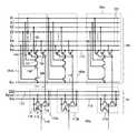
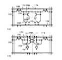
ここで本発明で用いる駆動回路について図1、図2を用いて説明する。本発明では一般
的なシフトレジスタの代わりに図1に示すようなpチャネル型TFTを用いたデコーダを
用いる。なお、図1はゲート側駆動回路の例である。Here, a driving circuit used in the present invention will be described with reference to FIGS. In the present invention, a decoder using a p-channel TFT as shown in FIG. 1 is used instead of a general shift register. FIG. 1 shows an example of a gate side driving circuit.
図1において、100がゲート側駆動回路のデコーダ、101がゲート側駆動回路のバ
ッファ部である。なお、バッファ部とは複数のバッファ(緩衝増幅器)
が集積化された部分を指す。また、バッファとは後段の影響を前段に与えずに駆動を行う
回路を指す。In FIG. 1, 100 is a decoder of the gate side driving circuit, and 101 is a buffer section of the gate side driving circuit. The buffer unit is a plurality of buffers (buffer amplifiers).
Indicates an integrated part. In addition, the buffer refers to a circuit that performs driving without affecting the preceding stage.
まずゲート側デコーダ100を説明する。まず102はデコーダ100の入力信号線(
以下、選択線という)であり、ここではA1、A1バー(A1の極性が反転した信号)、
A2、A2バー(A2の極性が反転した信号)、…An、Anバー(Anの極性が反転し
た信号)を示している。即ち、2n本の選択線が並んでいると考えれば良い。First, the
Hereinafter, it is referred to as a selection line), and here, A1, A1 bar (a signal in which the polarity of A1 is inverted),
A2 and A2 bars (signals with inverted polarity of A2),..., An and An bars (signals with inverted polarity of An) are shown. That is, it can be considered that 2n selection lines are arranged.
選択線の本数はゲート側駆動回路から出力されるゲート配線が何列あるかによってその
数が決まる。例えばVGA表示の画素部をもつ場合はゲート配線が480本となるため、
9bit分(n=9に相当する)で合計18本の選択線が必要となる。選択線102は図2
のタイミングチャートに示す信号を伝送する。図2に示すように、A1の周波数を1とす
ると、A2の周波数は2-1倍、A3の周波数は2-2倍、Anの周波数は2-(n-1)倍となる
。The number of selection lines is determined by the number of gate lines output from the gate side driving circuit. For example, in the case of having a pixel portion for VGA display, there are 480 gate wirings.
A total of 18 selection lines are required for 9 bits (corresponding to n = 9). The
The signal shown in the timing chart is transmitted. As shown in FIG. 2, when the frequency of A1 is 1, the frequency of A2 is 2−1 times, the frequency of A3 is 2−2 times, and the frequency of An is 2− (n−1) times.
また、103aは第1段のNAND回路(NANDセルともいう)、103bは第2段の
NAND回路、103cは第n段のNANDである。NAND回路はゲート配線の本数分
が必要であり、ここではn個が必要となる。即ち、本発明ではデコーダ100が複数のN
AND回路からなる。
It consists of an AND circuit.
また、NAND回路103a〜103cは、pチャネル型TFT104〜109が組み合
わされてNAND回路を形成している。なお、実際には2n個のTFTがNAND回路1
03に用いられている。また、pチャネル型TFT104〜109の各々のゲートは選択
線102(A1、A1バー、A2、A2バー…An、Anバー)のいずれかに接続されて
いる。The
03. Each gate of the p-
このとき、NAND回路103aにおいて、A1、A2…An(これらを正の選択線と
呼ぶ)のいずれかに接続されたゲートを有するpチャネル型TFT104〜106は、互
いに並列に接続されており、共通のソースとして正電源線(VDH)110に接続され、共
通のドレインとして出力線111に接続されている。
また、A1バー、A2バー…Anバー(これらを負の選択線と呼ぶ)のいずれかに接続さ
れたゲートを有するpチャネル型TFT107〜109は、互いに直列に接続されており
、回路端に位置するpチャネル型TFT109のソースが負電源線(VDL)112に接続
され、もう一方の回路端に位置するpチャネル型TFT107のドレインが出力線111
に接続されている。At this time, in the
In addition, p-
It is connected to the.
以上のように、本発明においてNAND回路は直列に接続されたn個の一導電型TFT
(ここではpチャネル型TFT)および並列に接続されたn個の一導電型TFT(ここで
はpチャネル型TFT)を含む。但し、n個のNAND回路103a〜103cにおいて、
pチャネル型TFTと選択線との組み合わせはすべて異なる。即ち、出力線111は必ず
1本しか選択されないようになっており、選択線102には出力線111が端から順番に
選択されていくような信号が入力される。As described above, in the present invention, the NAND circuit includes n one-conductivity TFTs connected in series.
(Here, p-channel type TFT) and n one-conductivity type TFTs (here, p-channel type TFTs) connected in parallel. However, in the
All combinations of p-channel TFTs and selection lines are different. In other words, only one
次に、バッファ101はNAND回路103a〜103cの各々に対応して複数のバッフ
ァ113a〜113cにより形成されている。但しバッファ113a〜113cはいずれも同
一構造で良い。Next, the
また、バッファ113a〜113cは一導電型TFTとしてpチャネル型TFT114〜
116を用いて形成される。デコーダからの出力線111はpチャネル型TFT114(
第1の一導電型TFT)のゲートとして入力される。pチャネル型TFT114は接地電
源線(GND)117をソースとし、ゲート配線118をドレインとする。また、pチャ
ネル型TFT115(第2の一導電型TFT)は接地電源線117をゲートとし、正電源
線(VDH)119をソースとし、ゲート配線118をドレインとして常時オン状態となっ
ている。The
116. The
It is input as the gate of the first one conductivity type TFT). The p-
即ち、本発明において、バッファ113a〜113cは第1の一導電型TFT(pチャネ
ル型TFT114)および第1の一導電型TFTに直列に接続され、且つ、第1の一導電
型TFTのドレインをゲートとする第2の一導電型TFT(pチャネル型TFT115)
を含む。That is, in the present invention, the
including.
また、pチャネル型TFT116(第3の一導電型TFT)はリセット信号線(Reset
)をゲートとし、正電源線119をソースとし、ゲート配線118をドレインとする。な
お、接地電源線117は負電源線(但し画素のスイッチング素子として用いるpチャネル
型TFTがオン状態になるような電圧を与える電源線)としても構わない。The p-channel TFT 116 (third one-conductivity type TFT) is connected to a reset signal line (Reset
) As a gate, the positive
このとき、pチャネル型TFT115のチャネル幅(W1とする)とpチャネル型TF
T114のチャネル幅(W2とする)との間にはW1<W2の関係がある。なお、チャネ
ル幅とはチャネル長に垂直な方向におけるチャネル形成領域の長さである。At this time, the channel width (W1) of the p-
There is a relationship of W1 <W2 with the channel width (W2) of T114. Note that the channel width is the length of a channel formation region in a direction perpendicular to the channel length.
バッファ113aの動作は次の通りである。まず出力線111に正電圧が加えられてい
るとき、pチャネル型TFT114はオフ状態(チャネルが形成されていない状態)とな
る。一方でpチャネル型TFT115は常にオン状態(チャネルが形成されている状態)
であるため、ゲート配線118には正電源線119の電圧が加えられる。The operation of the
Therefore, the voltage of the positive
ところが、出力線111に負電圧が加えられた場合、pチャネル型TFT114がオン
状態となる。このとき、pチャネル型TFT114のチャネル幅がpチャネル型TFT1
15のチャネル幅よりも大きいため、ゲート配線118の電位はpチャネル型TFT11
4側の出力に引っ張られ、結果的に接地電源線117の電圧がゲート配線118に加えら
れる。However, when a negative voltage is applied to the
Since the channel width is larger than 15, the potential of the
As a result, the voltage of the ground
従って、ゲート配線118は、出力線111に負電圧が加えられるときは負電圧(画素
のスイッチング素子として用いるpチャネル型TFTがオン状態になるような電圧)を出
力し、出力線111に正電圧が加えられているときは常に正電圧(画素のスイッチング素
子として用いるpチャネル型TFTがオフ状態になるような電圧)を出力する。Therefore, when a negative voltage is applied to the
なお、pチャネル型TFT116は負電圧が加えられたゲート配線118を強制的に正
電圧に引き上げるリセットスイッチとして用いられる。即ち、ゲート配線118の選択期
間が終了したら。リセット信号を入力してゲート配線118に正電圧を加える。但しpチ
ャネル型TFT116は省略することもできる。Note that the p-
以上のような動作のゲート側駆動回路によりゲート配線が順番に選択されることになる
。次に、ソース側駆動回路の構成を図3に示す。図3に示すソース側駆動回路はデコーダ
301、ラッチ302およびバッファ303を含む。なお、デコーダ301およびバッフ
ァ303の構成はゲート側駆動回路と同様であるので、ここでの説明は省略する。The gate lines are sequentially selected by the gate side driving circuit operating as described above. Next, FIG. 3 shows the configuration of the source side driver circuit. The source side driver circuit shown in FIG. 3 includes a
図3に示すソース側駆動回路の場合、ラッチ302は第1段目のラッチ304および第
2段目のラッチ305からなる。また、第1段目のラッチ304および第2段目のラッチ
305は、各々m個のpチャネル型TFT306a〜306cで形成される複数の単位ユニ
ット307を有する。デコーダ301からの出力線308は単位ユニット307を形成す
るm個のpチャネル型TFT306a〜306cのゲートに入力される。なお、mは任意の
整数である。In the case of the source side driver circuit shown in FIG. 3, the
例えば、VGA表示の場合、ソース配線の本数は640本である。m=1の場合はNA
ND回路も640個必要となり、選択線は20本(10bit分に相当する)必要となる。
しかし、m=8とすると必要なNAND回路は80個となり、必要な選択線は14本(7
bit分に相当する)となる。即ち、ソース配線の本数をM本とすると、必要なNAND回
路は(M/m)個となる。For example, in the case of VGA display, the number of source lines is 640. NA if m = 1
640 ND circuits are required, and 20 selection lines (corresponding to 10 bits) are required.
However, if m = 8, the number of necessary NAND circuits is 80, and the number of necessary selection lines is 14 (7
equivalent to bit). That is, if the number of source wirings is M, the necessary NAND circuits are (M / m).
そして、pチャネル型TFT306a〜306cのソースは各々ビデオ信号線(V1、V
2…Vk)309に接続される。即ち、出力線308に負電圧が加えられると一斉にpチ
ャネル型TFT306a〜306cがオン状態となり、各々に対応するビデオ信号が取り込
まれる。また、こうして取り込まれたビデオ信号は、pチャネル型TFT306a〜30
6cの各々に接続されたコンデンサ310a〜310cに保持される。The sources of the p-
2... Vk) 309. That is, when a negative voltage is applied to the
6c is held by
また、第2段目のラッチ305も複数の単位ユニット307bを有し、単位ユニット3
07bはm個のpチャネル型TFT311a〜311cで形成される。pチャネル型TFT
311a〜311cのゲートはすべてラッチ信号線312に接続され、ラッチ信号線312
に負電圧が加えられると一斉にpチャネル型TFT311a〜311cがオン状態となる。The second-
07b is formed of m p-
All the
When a negative voltage is applied to the p-
その結果、コンデンサ310a〜310cに保持されていた信号が、pチャネル型TFT
311a〜311cの各々に接続されたコンデンサ313a〜313cに保持されると同時に
バッファ303へと出力される。そして、図1で説明したようにバッファを介してソース
配線314に出力される。以上のような動作のソース側駆動回路によりソース配線が順番
に選択されることになる。As a result, the signals held in the
It is held in
以上のように、pチャネル型TFTのみでゲート側駆動回路およびソース側駆動回路を
形成することにより画素部および駆動回路をすべてpチャネル型TFTで形成することが
可能となる。従って、アクティブマトリクス型の表示装置を作製する上でTFT工程の歩
留まりおよびスループットを大幅に向上させることができ、製造コストを低減することが
可能となる。As described above, by forming the gate side driver circuit and the source side driver circuit with only the p-channel TFT, the pixel portion and the driver circuit can all be formed with the p-channel TFT. Accordingly, the yield and throughput of the TFT process can be significantly improved in manufacturing an active matrix display device, and the manufacturing cost can be reduced.
なお、ソース側駆動回路もしくはゲート側駆動回路のいずれか片方の全部もしくは一部
を外付けのICチップとする場合にも本発明は実施できる。Note that the present invention can also be implemented when all or a part of either the source side driver circuit or the gate side driver circuit is an external IC chip.
本発明では駆動回路をすべてpチャネル型TFTで形成することを特徴としているが、
画素部もすべてpチャネル型TFTで形成する。そこで、本実施例では図1および図3に
示した駆動回路により伝送された信号により画像を表示するための画素部の構造について
説明する。The present invention is characterized in that all the drive circuits are formed of p-channel TFTs.
All the pixel portions are also formed by p-channel TFTs. Therefore, in this embodiment, a structure of a pixel portion for displaying an image by a signal transmitted by the driving circuit shown in FIGS. 1 and 3 will be described.
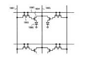
ここで本発明のアクティブマトリクス型発光装置の画素構造を図5および図6に示す。
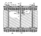
図5は一画素の断面図を示しており、図6は隣接する二つの画素の上面図を示している。
なお、図5は図6をA−A’で切断した断面図を表し、各図面において同一の箇所には同
一の符号を付してある。また、図6の二つの画素は電流供給線525に対して線対称なの
で、どちらも構造は同一である。Here, FIG. 5 and FIG. 6 show a pixel structure of the active matrix light-emitting device of the present invention.
FIG. 5 shows a cross-sectional view of one pixel, and FIG. 6 shows a top view of two adjacent pixels.
FIG. 5 is a cross-sectional view taken along line AA ′ of FIG. 6, and the same reference numerals are given to the same portions in the respective drawings. Further, since the two pixels in FIG. 6 are line-symmetric with respect to the
図5において、501は可視光に対して透明な基板、502は珪素を含む絶縁膜である
。可視光に対して透明な基板501としてはガラス基板、石英基板、結晶化ガラス基板も
しくはプラスチック基板(プラスチックフィルムも含む)を用いることができる。また、
珪素を含む絶縁膜502としては、酸化珪素膜、窒化酸化珪素膜もしくは窒化珪素膜を用
いることができる。In FIG. 5,
As the insulating
なお、本明細書ではTFTを絶縁体の上に形成する。絶縁体は絶縁膜(代表的には珪素
を含む絶縁膜)の場合もあるし、絶縁物からなる基板(代表的には石英基板)の場合もあ
る。従って、絶縁体の上とは、絶縁膜の上もしくは絶縁物からなる基板の上を指す。Note that in this specification, a TFT is formed over an insulator. The insulator may be an insulating film (typically an insulating film containing silicon) or a substrate made of an insulator (typically a quartz substrate). Therefore, the term “on the insulator” means above the insulating film or the substrate made of an insulator.
この珪素を含む絶縁膜502の上にはスイッチング用TFT601および電流制御用T
FT602がpチャネル型TFTで形成されている。On the insulating
The FT 602 is formed of a p-channel TFT.
スイッチング用TFT601は、p型半導体からなる領域(以下、p型半導体領域とい
う)503〜505および真性または実質的に真性な半導体からなる領域(以下、チャネ
ル形成領域という)506、507を含む半導体領域を活性層としている。また、電流制
御用TFT602はp型半導体領域508、509およびチャネル形成領域510を含む
半導体領域を活性層としている。The switching TFT 601 includes semiconductor regions including regions made of p-type semiconductor (hereinafter referred to as p-type semiconductor regions) 503 to 505 and regions made of intrinsic or substantially intrinsic semiconductors (hereinafter referred to as channel formation regions) 506 and 507. Is the active layer. The current control TFT 602 uses a semiconductor region including the p-
なお、p型半導体領域503もしくは505はスイッチング用TFT601のソース領
域もしくはドレイン領域となる。また、p型半導体領域508は電流制御用TFT602
のソース領域となり、p型半導体領域509は同TFTのドレイン領域となる。Note that the p-
The p-
スイッチング用TFT601及び電流制御用TFT602の活性層は、ゲート絶縁膜5
11に覆われ、その上にはソース配線512、ゲート電極513a、ゲート電極513b、
ドレイン配線514およびゲート電極515が形成されている。これらは同一の材料で同
時に形成される。なお、これらの配線や電極の材料としては、タンタル、タングステン、
モリブデン、ニオブ、チタンもしくはこれら金属の窒化物を用いれば良い。また、これら
金属を組み合わせた合金を用いても良いし、これら金属のシリサイドを用いても良い。The active layers of the switching TFT 601 and the current control TFT 602 are the
11 and a
A
Molybdenum, niobium, titanium, or nitrides of these metals may be used. An alloy in which these metals are combined may be used, or a silicide of these metals may be used.
また、図6に示すように、ドレイン配線514はゲート電極515と一体となっている
。また、ゲート電極513aおよびゲート電極513bは共通のゲート配線516と一体と
なっており、常に同じ電圧が加えられる。As shown in FIG. 6, the
また、図5において、517は窒化酸化珪素膜もしくは窒化珪素膜からなるパッシベー
ション膜であり、その上には層間絶縁膜518が設けられている。層間絶縁膜518とし
ては、珪素を含む絶縁膜もしくは有機樹脂膜を用いる。有機樹脂膜としては、ポリイミド
、ポリアミド、アクリル樹脂もしくはBCB(ベンゾシクロブテン)を用いれば良い。In FIG. 5,
また、その上には透明導電膜からなる接続配線519〜522および電極523が形成
されている。またこのとき同時に図6に示す配線524も形成されている。なお、透明導
電膜としては、酸化インジウム、酸化スズ、酸化亜鉛、酸化インジウムと酸化スズの化合
物、酸化インジウムと酸化亜鉛の化合物もしくはこれらにガリウムを添加した化合物から
なる薄膜を用いることができる。In addition, connection wirings 519 to 522 and an
このとき、接続配線520はソース配線512とp型半導体領域503を電気的に接続
する配線であり、接続配線521はp型半導体領域505とドレイン配線514を電気的
に接続する配線であり、接続配線522はソース領域508と電流供給線(図6参照)5
25を電気的に接続する配線である。At this time, the
25 is a wiring for electrically connecting 25.
また、接続配線519は複数のパターンに分割して形成されたゲート配線516を相互
に接続するための配線であり、ソース配線512および電流供給線525を跨ぐようにし
て設けられる。なお、ゲート配線を跨ぐように形成された接続配線により複数に分割して
形成されたソース配線もしくは電流供給線を相互に接続する構造とすることも可能である
。The
また、電極523はEL素子の陽極であり、本明細書では画素電極もしくは陽極と呼ぶ
。画素電極523は電流制御用TFT602のドレイン領域509に電気的に接続されて
いる。なお、図6では画素電極523が電流制御TFT602のドレイン配線であるとも
言える。The
ここで図6をB−B’で切断した断面図を図7(A)に示す。図7(A)のように接続
配線524は電流供給線525を跨いでゲート配線516を相互に接続している。また、
図6をC−C’で切断した断面図を図7(B)に示す。図7(B)のように接続配線52
2は電流制御用TFT602のp型半導体領域508および電流供給線525を電気的に
接続する。Here, FIG. 7A shows a cross-sectional view of FIG. 6 cut along BB ′. As shown in FIG. 7A, the
A cross-sectional view taken along the line CC ′ of FIG. 6 is shown in FIG. Connection wiring 52 as shown in FIG.
2 electrically connects the p-
実際には、このあと画素電極523の上にEL層(図示せず)および陰極(図示せず)
を形成してアクティブマトリクス型発光装置が完成する。EL層および陰極の形成は公知
の技術を用いても良い。Actually, after this, an EL layer (not shown) and a cathode (not shown) are formed on the
To complete an active matrix light-emitting device. A known technique may be used to form the EL layer and the cathode.
また、ここではTFTとしてトップゲート構造のTFT(具体的にはプレーナ型TFT
)を例示したが、本発明はTFT構造に限定されるものではなく、ボトムゲート構造のT
FTにも実施できる。代表的には逆スタガ型TFTに実施することは可能である。Here, as a TFT, a TFT having a top gate structure (specifically, a planar TFT)
However, the present invention is not limited to the TFT structure.
It can also be applied to FT. Typically, it can be applied to an inverted staggered TFT.
以上の画素構造とすることで、アクティブマトリクス型発光装置の製造工程を大幅に低
減することが可能となり、安価なアクティブマトリクス型発光装置を生産することが可能
となる。また、それを表示部に用いた電気器具をも安価なものとすることができる。With the above pixel structure, the manufacturing process of the active matrix light-emitting device can be significantly reduced, and an inexpensive active matrix light-emitting device can be produced. In addition, an electric appliance using the display unit for the display portion can be made inexpensive.
本実施例では、同一の絶縁体上に画素部および画素部に信号を伝送する駆動回路を設け
たアクティブマトリクス型発光装置の作製工程について図8、図9を用いて説明する。In this embodiment, a manufacturing process of an active matrix light-emitting device in which a pixel portion and a driver circuit that transmits a signal to the pixel portion are provided over the same insulator will be described with reference to FIGS.
まず、図8(A)に示すように、ガラス基板801上に、下地膜(絶縁体)802を形
成する。本実施例ではガラス基板801側から50nmの第1の窒化酸化珪素膜、200
nmの第2の窒化酸化珪素膜を順次積層して下地膜802とする。また、第1の窒化酸化
珪素膜の方が第2の窒化酸化珪素膜に比べて窒素の含有量を多くし、ガラス基板801か
らのアルカリ金属の拡散を抑制している。First, as shown in FIG. 8A, a base film (insulator) 802 is formed over a
A second silicon nitride oxide film having a thickness of nm is sequentially stacked to form a
次に、下地膜802上に非晶質珪素膜(図示せず)をプラズマCVD法により40nm
の厚さに形成する。そして、非晶質珪素膜にレーザー光を照射することにより結晶化させ
、多結晶珪素膜(ポリシリコン膜)803を形成する。なお、非晶質珪素膜の代わりに微
結晶珪素膜もしくは非晶質のシリコンゲルマニウム膜を形成しても良い。また、結晶化方
法はレーザー結晶化法に限定する必要はなく、公知の他の結晶化法を用いることもできる
。Next, an amorphous silicon film (not shown) is formed on the
The thickness is formed. Then, the amorphous silicon film is crystallized by irradiating a laser beam to form a polycrystalline silicon film (polysilicon film) 803. Note that a microcrystalline silicon film or an amorphous silicon germanium film may be formed instead of the amorphous silicon film. Further, the crystallization method is not limited to the laser crystallization method, and other known crystallization methods can also be used.
次に、図8(B)に示すように、多結晶珪素膜803をパターニングして個々に孤立し
た半導体層804〜806を形成する。なお、804で示される半導体層は、完成時に駆
動回路を形成するTFT(以下、駆動TFTという)の活性層となり、805はスイッチ
ングTFTの活性層、806は電流制御TFTの活性層となる。Next, as shown in FIG. 8B, the
そして孤立した半導体層804〜806を覆って酸化珪素膜からなるゲート絶縁膜80
7をプラズマCVD法により80nmの厚さに形成する。さらに、ゲート絶縁膜807の
上にスパッタ法によりタングステン膜(図示せず)を350nmの厚さに形成し、パター
ニングしてゲート電極808、809、810aおよび810bを形成する。また同時に、
スイッチングTFTのソース配線812およびドレイン配線813を形成する。もちろん
、ドレイン配線813とゲート電極811は一体形成されている。Then, a gate insulating film 80 made of a silicon oxide film is formed so as to cover the isolated semiconductor layers 804 to 806.
7 is formed to a thickness of 80 nm by plasma CVD. Further, a tungsten film (not shown) is formed to a thickness of 350 nm on the
A
次に、ゲート電極808、809、810a、810b、ソース配線812およびドレイ
ン配線813をマスクとして周期表の13族に属する元素を添加する。
添加方法は公知の手段を用いれば良い。本実施例ではプラズマドーピング法により5×1
019〜1×10²¹atoms/cm3の濃度でボロンを添加する。こうしてp型の導電型を示す半
導体領域(以下、p型半導体領域という)814〜821が形成される。また、ゲート電
極808、809、810aおよび810bの直下にはチャネル形成領域822〜826が
形成される。Next, elements belonging to Group 13 of the periodic table are added using the
The addition method may be a known means. In this embodiment, 5 × 1 by plasma doping.
Boron is added at a concentration of 019 to 1 × 10²¹ atoms / cm3 . In this way, semiconductor regions (hereinafter referred to as p-type semiconductor regions) 814 to 821 having p-type conductivity are formed. In addition,
なお、本実施例ではp型半導体領域814、816は駆動回路を形成するpチャネル型
TFTのソース領域として機能し、p型半導体領域815は駆動回路を形成するpチャネ
ル型TFTのドレイン領域として機能する。In this embodiment, the p-
次に、加熱処理を行ってp型半導体領域に含まれる周期表の13族に属する元素の活性
化を行う。この活性化はファーネスアニール、レーザーアニールもしくはランプアニール
により行うか、又はそれらを組み合わせて行えば良い。本実施例では500℃4時間の加
熱処理を窒素雰囲気で行う。このとき、窒素雰囲気中の酸素は極力低減しておくことが望
ましい。この活性化工程によりTFTの活性層が形成される。Next, heat treatment is performed to activate elements belonging to Group 13 of the periodic table included in the p-type semiconductor region. This activation may be performed by furnace annealing, laser annealing or lamp annealing, or a combination thereof. In this embodiment, the heat treatment at 500 ° C. for 4 hours is performed in a nitrogen atmosphere. At this time, it is desirable to reduce oxygen in the nitrogen atmosphere as much as possible. The active layer of the TFT is formed by this activation process.
活性化が終了したら、パッシベーション膜827として窒化酸化珪素膜を200nmの
厚さに形成し、その後、半導体層の水素化処理を行う。水素化処理は公知の水素アニール
技術もしくはプラズマ水素化技術を用いれば良い。こうして図8(C)の状態が得られる
。When the activation is completed, a silicon nitride oxide film is formed to a thickness of 200 nm as the
次に、図8(D)に示すように、樹脂からなる層間絶縁膜828を800nmの厚さに
形成する。樹脂としては、ポリイミド、ポリアミド、アクリル樹脂、エポキシ樹脂もしく
はBCB(ベンゾシクロブテン)を用いれば良い。また、無機の絶縁膜を用いても構わな
い。Next, as shown in FIG. 8D, an
次に、層間絶縁膜828にコンタクトホールを形成して接続配線829〜835および
画素電極836を形成する。本実施例では接続配線829〜835および画素電極836
として酸化インジウムと酸化スズの化合物(Indium Tin Oxide:ITO)からなる導電膜
を用いる。勿論、可視光に対して透明な導電膜であれば如何なる材料を用いても良い。Next, contact holes are formed in the
A conductive film made of a compound of indium oxide and tin oxide (Indium Tin Oxide: ITO) is used. Of course, any material may be used as long as the conductive film is transparent to visible light.
なお、接続配線829、831は駆動回路を形成するpチャネル型TFTのソース配線
として機能し、接続配線830は駆動回路を形成するpチャネル型TFTのドレイン配線
として機能する。このように本実施例ではpチャネル型TFTで形成されたPMOS回路
を基本として駆動回路を形成する。Note that the
この状態で駆動回路を形成するpチャネル型TFT、画素部に形成されるスイッチング
TFT及び電流制御TFTが完成する。本実施例ではすべてのTFTがpチャネル型TF
Tで形成される。但し、スイッチングTFTはゲート電極が活性層を二カ所で横切るよう
に形成されており、二つのチャネル形成領域が直列に接続された構造となっている。この
ような構造とすることでオフ電流値(TFTがオフされた時に流れる電流)を効果的に抑
制することができる。In this state, a p-channel TFT that forms a driving circuit, a switching TFT and a current control TFT formed in a pixel portion are completed. In this embodiment, all TFTs are p-channel type TF.
T is formed. However, the switching TFT has a structure in which the gate electrode crosses the active layer at two locations, and two channel formation regions are connected in series. With such a structure, an off-current value (current that flows when the TFT is turned off) can be effectively suppressed.
次に、図9(A)に示すように、画素電極836の端部および凹部(コンタクトホール
に起因する窪み)を隠すように樹脂からなる絶縁体837、838を形成する。これは樹
脂からなる絶縁膜を形成した後、パターニングを行って形成すれば良い。このとき、画素
電極836の表面から絶縁体838の頂上まで高さ(d)を300nm以下(好ましくは
200nm以下)とすることが望ましい。なお、この絶縁体837、838は省略するこ
とも可能である。Next, as shown in FIG. 9A,
絶縁体837は画素電極836の端部を隠し、端部における電界集中の影響を避ける目
的で形成する。これによりEL層の劣化を抑制することができる。また、絶縁体838は
コンタクトホールに起因して形成される画素電極の凹部を埋め込む目的で形成する。これ
により後に形成されるEL層の被覆不良を防止し、画素電極と後に形成される陰極の短絡
を防止することができる。The
次に、70nm厚のEL層839及び300nm厚の陰極840を蒸着法により形成す
る。本実施例ではEL層839として20nm厚の銅フタロシアニン(正孔注入層)及び
50nm厚のAlq3(発光層)を積層した構造を用いる。勿論、発光層に正孔注入層、
正孔輸送層、電子輸送層もしくは電子注入を組み合わせた公知の他の構造を用いても良い
。Next, an
Other known structures combining hole transport layers, electron transport layers, or electron injection may be used.
本実施例では、まず全ての画素電極を覆うように銅フタロシアニンを形成し、その後、
赤色、緑色及び青色に対応する画素ごとに各々赤色の発光層、緑色の発光層及び青色の発
光層を形成する。形成する領域の区別は蒸着時にシャドーマスクを用いて行えば良い。こ
のようにすることでカラー表示が可能となる。In this embodiment, first, copper phthalocyanine is formed so as to cover all the pixel electrodes, and then
A red light emitting layer, a green light emitting layer, and a blue light emitting layer are formed for each pixel corresponding to red, green, and blue. The regions to be formed may be distinguished using a shadow mask during vapor deposition. In this way, color display is possible.
なお、緑色の発光層を形成する時は、発光層の母体材料としてAlq3(トリス−8−
キノリノラトアルミニウム錯体)を用い、キナクリドンもしくはクマリン6をドーパント
として添加する。また、赤色の発光層を形成する時は、発光層の母体材料としてAlq3
を用い、DCJT、DCM1もしくはDCM2をドーパントとして添加する。また、青色
の発光層を形成する時は、発光層の母体材料としてBAlq3(2−メチル−8−キノリ
ノールとフェノール誘導体の混合配位子を持つ5配位の錯体)を用い、ペリレンをドーパ
ントとして添加する。When the green light emitting layer is formed, Alq3 (Tris-8-
Quinolinolato aluminum complex) and quinacridone or coumarin 6 is added as a dopant. When a red light emitting layer is formed, Alq3 is used as a base material of the light emitting layer.
And DCJT, DCM1 or DCM2 is added as a dopant. When a blue light emitting layer is formed, BAlq3 (a pentacoordinate complex having a mixed ligand of 2-methyl-8-quinolinol and a phenol derivative) is used as a base material of the light emitting layer, and perylene is used as a dopant. Add as
勿論、本願発明では上記有機材料に限定する必要はなく、公知の低分子系有機EL材料
、高分子系有機EL材料もしくは無機EL材料を用いることが可能である。また、これら
の材料を組み合わせて用いることも可能である。なお、高分子系有機EL材料を用いる場
合は塗布法を用いることもできる。Of course, in the present invention, it is not necessary to limit to the above organic material, and it is possible to use a known low molecular organic EL material, high molecular organic EL material or inorganic EL material. Moreover, it is also possible to use these materials in combination. In the case of using a polymer organic EL material, a coating method can also be used.
以上のようにして、画素電極(陽極)836、EL層839及び陰極840からなるE
L素子が形成される。(図9(B))As described above, E composed of the pixel electrode (anode) 836, the
An L element is formed. (Fig. 9 (B))
次に、図9(C)に示すように、接着剤841によりカバー材842を貼り合わせる。
本実施例ではカバー材842としてガラス基板を用いるが、可撓性のプラスチックフィル
ム、石英基板、プラスチック基板、金属基板、シリコン基板もしくはセラミックス基板を
用いても良い。なお、外気に触れる面に珪素を含む絶縁膜や炭素膜を設けて、酸素および
水の侵入を防止したり、摩擦により付く傷を防止したりすることも有効である。Next, as illustrated in FIG. 9C, the
Although a glass substrate is used as the
また、接着剤841としては、代表的には紫外線硬化樹脂または熱硬化樹脂を用いるこ
とができ、PVC(ポリビニルクロライド)、アクリル樹脂、ポリイミド、エポキシ樹脂
、シリコーン樹脂、PVB(ポリビニルブチラル)またはEVA(エチレンビニルアセテ
ート)を用いることができる。なお、接着剤841がEL素子から見て観測者側に位置す
る場合は、光を透過する材料であることが必要である。また、接着剤841の内部に吸湿
性物質(好ましくは酸化バリウム)
や酸化防止剤(酸素を吸着する物質)を設けておくとEL素子の劣化を抑制する上で効果
的である。As the adhesive 841, typically, an ultraviolet curable resin or a thermosetting resin can be used. PVC (polyvinyl chloride), acrylic resin, polyimide, epoxy resin, silicone resin, PVB (polyvinyl butyral), or EVA (Ethylene vinyl acetate) can be used. Note that in the case where the adhesive 841 is positioned on the observer side as viewed from the EL element, it is necessary that the adhesive 841 be a material that transmits light. Further, a hygroscopic substance (preferably barium oxide) is contained in the adhesive 841.
If an antioxidant (a substance that adsorbs oxygen) is provided, it is effective in suppressing deterioration of the EL element.
このような構造とすることによりEL素子を完全に大気から遮断することができる。こ
れにより酸化によるEL材料の劣化をほぼ完全に抑制することができ、EL素子の信頼性
を大幅に向上させることができる。With such a structure, the EL element can be completely shielded from the atmosphere. Thereby, deterioration of the EL material due to oxidation can be suppressed almost completely, and the reliability of the EL element can be greatly improved.
以上のようにして作製されたアクティブマトリクス型発光装置は、図10に示す回路構
成の画素部を有する。図10において、1001はソース配線、1002はゲート配線、
1003はスイッチングTFT、1004は電流制御TFT、1005は電流供給線、1
006はEL素子である。本実施例ではスイッチングTFT1003および電流制御TF
T1004がpチャネル型TFTで作製されている。The active matrix light-emitting device manufactured as described above has a pixel portion having a circuit configuration shown in FIG. In FIG. 10, 1001 is a source wiring, 1002 is a gate wiring,
1003 is a switching TFT, 1004 is a current control TFT, 1005 is a current supply line,
006 is an EL element. In this embodiment, the switching
T1004 is made of a p-channel TFT.
なお、本実施例では従来用いられていたコンデンサ(図4のコンデンサ404)と同じ
役割を、電流制御TFT1004のゲート容量で補っている。これは、デジタル駆動によ
り時分割階調表示を行う場合、1フレーム期間(もしくは1フィールド期間)が短いため
、電流制御TFTのゲート容量だけで電荷を保持しうるためである。In this embodiment, the same function as that of the conventionally used capacitor (
このような本発明のアクティブマトリクス型発光装置は、パターニングに必要なマスク
数がトータルで5枚(絶縁体837、838を省略すれば4枚)と非常に少なく、高い歩
留まりと低い製造コストを達成することができる。In such an active matrix light emitting device of the present invention, the total number of masks necessary for patterning is very small as five (four if the
実施例2において、図10に示した画素部の回路構成は、図11に示した回路構成とし
ても良い。図11において、1101はソース配線、1102はゲート配線、1103は
スイッチングTFT、1104は電流制御TFT、1105は電流供給線、1106はE
L素子である。本実施例ではスイッチングTFT1103および電流制御TFT1104
がpチャネル型TFTで作製されている。In Example 2, the circuit configuration of the pixel portion illustrated in FIG. 10 may be the circuit configuration illustrated in FIG. In FIG. 11, 1101 is a source wiring, 1102 is a gate wiring, 1103 is a switching TFT, 1104 is a current control TFT, 1105 is a current supply line, and 1106 is E
L element. In this embodiment, the switching
Are made of p-channel TFTs.
このとき、ゲート配線1102と電流供給線1105は異なる層に形成されるため、両
者が層間絶縁膜を挟んで重なるように設けることは有効である。このようにすることで実
質的に配線の占有面積を共通化することができ、画素の有効発光面積を増やすことができ
る。At this time, since the
本実施例では、実施例1とは異なる工程でアクティブマトリクス型発光装置を作製した
場合について説明する。説明には図12を用いる。In this example, a case where an active matrix light-emitting device is manufactured through a process different from that of Example 1 is described. FIG. 12 is used for the description.
まず、実施例2に従って図8(D)の工程まで行い、接続配線1201〜1207およ
びドレイン配線1208を形成する。本実施例では、これらの接続配線を、金属膜を用い
て形成する。金属膜としては如何なる材料を用いても良い。本実施例では、アルミニウム
膜をチタン膜で挟んだ三層構造の積層膜を用いる。First, the process up to the step of FIG. In this embodiment, these connection wirings are formed using a metal film. Any material may be used for the metal film. In this embodiment, a laminated film having a three-layer structure in which an aluminum film is sandwiched between titanium films is used.
次に、図12(B)に示すように、透明導電膜からなる画素電極1209を形成する。
このとき、画素電極1209の一部がドレイン配線1208と接するように形成する。こ
れにより電流制御TFTと画素電極とが電気的に接続される。
この状態の上面図を図13に示す。なお、図13をA−A’で切断した断面図が図12(
B)の断面図に相当する。Next, as shown in FIG. 12B, a
At this time, part of the
A top view of this state is shown in FIG. 13 is a cross-sectional view taken along line AA ′ in FIG.
It corresponds to the sectional view of B).
本実施例では接続配線1201〜1207を金属膜で形成することができるため、実施
の形態で説明したITO等の透明導電膜に比べて配線抵抗の低減およびコンタクト抵抗の
低減を図ることができる。もちろん、駆動回路においても回路間を結ぶ配線をすべて低抵
抗な金属膜で形成することができるため、動作速度の速い駆動回路を形成することが可能
となる。In this embodiment, since the
なお、本実施例では接続配線1201〜1207およびドレイン配線1208を形成し
た後で画素電極1209を形成しているが、この順序を逆にすることもできる。即ち、透
明導電膜からなる画素電極を形成した後に金属膜からなる接続配線およびドレイン配線を
形成しても良い。In this embodiment, the
このあとは実施例2と同様に、樹脂からなる絶縁体1210を形成し、EL層1211
、陰極1212を順次形成していく。さらに、接着剤1213を用いてカバー材1214
を形成する。こうして図12(C)に示すアクティブマトリクス型発光装置が完成する。Thereafter, as in Example 2, an
The
Form. Thus, the active matrix light-emitting device shown in FIG. 12C is completed.
本実施例では、プラスチック基板もしくはプラスチックフィルムを用いて本発明のアク
ティブマトリクス型発光装置を作製する例について説明する。なお、本実施例で用いるこ
とのできるプラスチックとしては、PES(ポリエチレンサルファイル)、PC(ポリカ
ーボネート)、PET(ポリエチレンテレフタレート)もしくはPEN(ポリエチレンナ
フタレート)を用いることができる。In this embodiment, an example in which an active matrix light-emitting device of the present invention is manufactured using a plastic substrate or a plastic film will be described. In addition, as a plastic which can be used in a present Example, PES (polyethylene sulfide), PC (polycarbonate), PET (polyethylene terephthalate), or PEN (polyethylene naphthalate) can be used.
まず実施例2の工程に従ってガラス基板801上にTFTおよびEL素子を形成する。
ただし、本実施例では図14(A)に示すように、ガラス基板801と下地膜802の間
に剥離層1401を形成する。なお、剥離層1401としては半導体膜を用いることが可
能であり、代表的には非晶質珪素膜を用いれば良い。First, TFTs and EL elements are formed on a
However, in this embodiment, a
また、本実施例では第1の接着剤1402によりカバー材1403を接着するが、第1
の接着剤1402として樹脂からなる絶縁膜(代表的にはポリイミド、アクリル樹脂、ポ
リアミドもしくはエポキシ樹脂)を用いる。ただし、後に剥離層1401をフッ化ハロゲ
ンを含むガスでエッチングした際に選択比のとれる材料を用いることが必要である。また
、本実施例では第1の接着剤1402により接着するカバー材1403としてPETフィ
ルムを用いる。In this embodiment, the
As the adhesive 1402, an insulating film made of a resin (typically polyimide, acrylic resin, polyamide, or epoxy resin) is used. However, it is necessary to use a material that can have a selection ratio when the
次に、図14(B)に示すように、素子が形成された基板全体をフッ化ハロゲンを含む
ガス中に晒す。この処理により剥離層1401を選択的に除去することができる。フッ化
ハロゲンとは化学式XFn(Xはフッ素以外のハロゲン、nは整数)で示される物質であ
り、一フッ化塩素(ClF)、三フッ化塩素(ClF3)、一フッ化臭素(BrF)、三
フッ化臭素(BrF3)、一フッ化ヨウ素(IF)もしくは三フッ化ヨウ素(IF3)を用
いることができる。Next, as shown in FIG. 14B, the entire substrate on which the element is formed is exposed to a gas containing halogen fluoride. By this treatment, the
このフッ化ハロゲンは、シリコン膜と酸化シリコン膜との選択比が大きく、シリコン膜
の選択的なエッチングが可能である。また、このエッチング反応は室温で容易に進行する
ため耐熱性の低いEL素子を形成した後でも処理を行うことが可能である。This halogen fluoride has a large selection ratio between the silicon film and the silicon oxide film, and can selectively etch the silicon film. Further, since this etching reaction easily proceeds at room temperature, it is possible to perform the treatment even after forming an EL element with low heat resistance.
なお、上述のフッ化ハロゲンにシリコン膜を晒すだけでシリコン膜はエッチングされる
が、他のフッ化物(四フッ化炭素(CF4)もしくは三フッ化窒素)であってもプラズマ
状態とすることで本願発明に用いることは可能である。The silicon film is etched only by exposing the silicon film to the above-mentioned halogen fluoride. However, even if other fluorides (carbon tetrafluoride (CF4) or nitrogen trifluoride) are used, the silicon film is brought into a plasma state. It can be used in the present invention.
本実施例では、フッ化ハロゲンとして三フッ化塩素(ClF3)を用い、希釈ガスとし
て窒素を用いる。希釈ガスとしては、アルゴン、ヘリウムもしくはネオンを用いても良い
。流量は共に500sccm(8.35×10⁻⁶m3/s)とし、反応圧力は1〜10T
orr(1.3×10²〜1.3×10³Pa)とすれば良い。また、処理温度は室温(典
型的には20〜27℃)で良い。In this embodiment, chlorine trifluoride (ClF3 ) is used as the halogen fluoride, and nitrogen is used as the dilution gas. Argon, helium, or neon may be used as the dilution gas. Both flow rates were 500 sccm (8.35 × 10⁻⁶ m3 / s), and the reaction pressure was 1 to 10 T.
Orr (1.3 × 10² to 1.3 × 10³ Pa) may be used. The processing temperature may be room temperature (typically 20 to 27 ° C.).
次に、図14(C)に示すように、第2の接着剤1404を用いてプラスチック基板も
しくはプラスチックフィルムからなる基板(貼り合わせ基板)1405を貼り合わせる。
本実施例では貼り合わせ基板1405としてPETフィルムを用いる。応力バランスをと
るためカバー材1403と貼り合わせ基板1405の材料は同一とすることが望ましい。Next, as shown in FIG. 14C, a substrate (bonded substrate) 1405 made of a plastic substrate or a plastic film is bonded using a
In this embodiment, a PET film is used as the bonded
以上のようにして、プラスチックフィルムにTFTおよびEL素子を挟んだアクティブ
マトリクス型発光装置が得られる。本実施例はTFTを形成した後でプラスチックフィル
ムを貼り合わせることになるため、プラスチックの耐熱性を考慮してTFTを作製すると
いった制限がない。As described above, an active matrix light-emitting device in which a TFT and an EL element are sandwiched between plastic films is obtained. In this embodiment, since the plastic film is bonded after the TFT is formed, there is no restriction that the TFT is manufactured in consideration of the heat resistance of the plastic.
またフレキシブルで軽量な発光装置が得られるため、携帯電話や電子手帳などの携帯情
報機器の表示部に適している。Further, since a light-emitting device that is flexible and lightweight can be obtained, the light-emitting device is suitable for a display portion of a portable information device such as a mobile phone or an electronic notebook.
なお、本実施例の構成は実施例1〜4のいずれの構成とも自由に組み合わせて実施する
ことができる。In addition, the structure of a present Example can be implemented in combination freely with any structure of Examples 1-4.
本発明において、TFTおよびEL素子を形成する基板またはカバー材の片面もしくは
両面にDLC(ダイヤモンドライクカーボン)膜を形成しておくことは有効である。但し
、膜厚が厚すぎると透過率が落ちるので、50nm以下(好ましくは10〜20nm)と
すると良い。また、DLC膜の成膜はスパッタ法もしくはECRプラズマCVD法を用い
れば良い。In the present invention, it is effective to form a DLC (diamond-like carbon) film on one side or both sides of a substrate or cover material on which TFTs and EL elements are formed. However, if the film thickness is too thick, the transmittance decreases, so it is preferable to set the thickness to 50 nm or less (preferably 10 to 20 nm). Further, the DLC film may be formed by sputtering or ECR plasma CVD.
DLC膜の特徴としては、1550cm-1くらいに非対称のピークを有し、1300c
m-1くらいに肩をもつラマンスペクトル分布を有する。また、微小硬度計で測定した時に
15〜25Paの硬度を示すという特徴をもつ。また、DLC膜は基板やカバー材に比べ
て硬度が大きく且つ熱伝導率も大きいため、表面保護や熱分散のための保護膜として設け
ておくことが有効である。As a feature of the DLC film, it has an asymmetric peak at about 1550 cm−1 and 1300c.
It has a Raman spectral distribution with shoulders around m-1 . Moreover, it has the characteristic of showing a hardness of 15-25 Pa when measured with a micro hardness meter. Further, since the DLC film has higher hardness and higher thermal conductivity than the substrate and the cover material, it is effective to provide the DLC film as a protective film for surface protection and heat dispersion.
なお、本実施例の構成は実施例1〜5のいずれの構成とも自由に組み合わせて実施する
ことが可能である。In addition, the structure of a present Example can be implemented in combination with any structure of Examples 1-5 freely.
本実施例では、実施例2で説明した本発明の発光装置の外観図を説明する。なお、図1
5(A)は本発明の発光装置の上面図であり、図15(B)はその断面図である。In this example, an external view of the light-emitting device of the present invention described in Example 2 will be described. In addition, FIG.
5A is a top view of the light emitting device of the present invention, and FIG. 15B is a cross-sectional view thereof.
図15(A)において、1501は基板、1502は画素部、1503はソース側駆動
回路、1504はゲート側駆動回路であり、それぞれの駆動回路は配線1505を経てF
PC(フレキシブルプリントサーキット)1506に至り、外部機器へと接続される。図
1のゲート側駆動回路は図15(A)のゲート側駆動回路1504に用いられ、図3のソ
ース側駆動回路は図15(A)のソース側駆動回路1503に用いられ、図5の画素部は
図15(A)の画素部1502に用いられる。このとき画素部1502、ソース側駆動回
路1503及びゲート側駆動回路1504を囲むようにして第1シール材1511、カバ
ー材1512、接着剤1513(図15(B)参照)及び第2シール材1514が設けら
れる。In FIG. 15A,
A PC (flexible printed circuit) 1506 is connected to an external device. The gate side driver circuit in FIG. 1 is used for the gate
また、図15(B)は図15(A)をA−A’で切断した断面図に相当する。
このとき、点線1500で囲まれた領域が図9(C)の断面図に相当する。従って、ここ
での詳細な説明は省略する。FIG. 15B corresponds to a cross-sectional view taken along line AA ′ of FIG.
At this time, a region surrounded by a dotted
EL素子の陰極は1514で示される領域において配線1505に電気的に接続される
。配線1505は陰極に所定の電圧を与えるための配線であり、異方導電性フィルム15
15を介してFPC1506に電気的に接続される。さらにEL素子は、第1シール材1
511及びそれによって基板1501に貼り合わされたカバー材1512で囲まれ、接着
剤1513により封入されている。The cathode of the EL element is electrically connected to the
15 is electrically connected to the
511 and a
また、接着剤1513の中にスペーサを含有させてもよい。このとき、スペーサを酸化
バリウムで形成すればスペーサ自体に吸湿性をもたせることが可能である。また、スペー
サを設けた場合、スペーサからの圧力を緩和するバッファ層として陰極上に樹脂膜を設け
ることも有効である。Further, a spacer may be included in the adhesive 1513. At this time, if the spacer is formed of barium oxide, the spacer itself can be hygroscopic. In the case where a spacer is provided, it is also effective to provide a resin film on the cathode as a buffer layer that relieves pressure from the spacer.
また、配線1505は異方導電性フィルム1515を介してFPC1506に電気的に
接続される。配線1505は画素部1502、ソース側駆動回路1503及びゲート側駆
動回路1504に送られる信号をFPC1506に伝え、FPC1506により外部機器
と電気的に接続される。The
また、本実施例では第1シール材1511の露呈部及びFPC1506の一部を覆うよ
うに第2シール材1514を設け、EL素子を徹底的に外気から遮断する構造となってい
る。こうして図15(B)の断面構造を有する発光装置となる。なお、本実施例の発光装
置は実施例1〜6のいずれの構成を組み合わせて作製しても構わない。In this embodiment, the
本実施例では、本発明の発光装置の画素構造について図16(A)、(B)に示す。本
実施例において、1601はスイッチングTFT1602のソース配線、1603はスイ
ッチングTFT1602のゲート配線、1604は電流制御TFT、1605はコンデン
サ(省略することも可能)、1606は電流供給線、1607は電源制御TFT、160
8はEL素子、1609は電源制御線とする。このとき、ソース配線1601、ゲート配
線1603、電流供給線1606および電源制御線1608が同一の層に同一の導電膜で
形成される。In this embodiment, the pixel structure of the light-emitting device of the present invention is shown in FIGS. In this embodiment, 1601 is a source wiring of the switching
Reference numeral 8 denotes an EL element, and 1609 denotes a power control line. At this time, the
なお、電源制御TFT1607の動作については特願平11−341272号を参照す
ると良い。ただし本実施例では電源制御TFTを電流制御TFTと同一構造のpチャネル
型TFTとする。Refer to Japanese Patent Application No. 11-341272 for the operation of the power
また、本実施例では電源制御TFT1607を電流制御TFT1604とEL素子16
08との間に設けているが、電源制御TFT1607とEL素子1608との間に電流制
御TFT1604が設けられた構造としても良い。また、電源制御TFT1607は電流
制御TFT1604と同一構造とするか、同一の活性層で直列させて形成するのが好まし
い。In this embodiment, the
The
また、図16(A)は、二つの画素間で電流供給線1606を共通とした場合の例であ
る。即ち、二つの画素が電流供給線1606を中心に線対称となるように形成されている
点に特徴がある。この場合、電流供給線の本数を減らすことができるため、画素部をさら
に高精細化することができる。また、図16(B)は、ゲート配線1603と平行に電流
供給線1610を設け、ソース配線1601と平行に電源制御線1611を設けた場合の
例である。FIG. 16A shows an example in which the
なお、本実施例の構成は実施例1〜7のいずれの構成とも自由に組み合わせて実施する
ことが可能である。In addition, the structure of a present Example can be implemented in combination with any structure of Examples 1-7 freely.
本実施例では、本発明の発光装置の画素構造について図17(A)、(B)に示す。な
お、本実施例において、1701はスイッチングTFT1702のソース配線、1703
はスイッチングTFT1702のゲート配線、1704は電流制御TFT、1705はコ
ンデンサ(省略することも可能)、1706は電流供給線、1707は消去TFT、17
08は消去用ゲート配線、1709はEL素子とする。このとき、ソース配線1701、
ゲート配線1703、電流供給線1706および消去用ゲート配線1708が同一の層に
同一の導電膜で形成される。In this embodiment, the pixel structure of the light-emitting device of the present invention is shown in FIGS. In this embodiment,
Is a gate wiring of the switching
Reference numeral 08 denotes an erase gate wiring, and 1709 denotes an EL element. At this time, the
The
なお、消去TFT1707の動作については特願平11−338786号を参照すると
良い。ただし本実施例では電源制御TFTを電流制御TFTと同一構造のpチャネル型T
FTとする。また、特願平11−338786号では消去用ゲート配線を消去用ゲート信
号線と呼んでいる。Refer to Japanese Patent Application No. 11-338786 for the operation of the erasing
FT. In Japanese Patent Application No. 11-338786, the erase gate wiring is called an erase gate signal line.
消去TFT1707のドレインは電流制御TFT1704のゲートに接続され、電流制
御TFT1704のゲート電圧を強制的に変化させることができるようになっている。な
お、消去TFT1707はpチャネル型TFTとし、オフ電流を小さくできるようにスイ
ッチング用TFT1702と同一構造とすることが好ましい。The drain of the erasing
また、図17(A)は、二つの画素間で電流供給線1706を共通とした場合の例であ
る。即ち、二つの画素が電流供給線1706を中心に線対称となるように形成されている
点に特徴がある。この場合、電流供給線の本数を減らすことができるため、画素部をさら
に高精細化することができる。また、図17(B)は、ゲート配線1703と平行に電流
供給線1710を設け、ソース配線1701と平行に消去ゲート配線1711を設けた場
合の例である。FIG. 17A shows an example in which the
なお、本実施例の構成は実施例1〜7のいずれの構成とも自由に組み合わせて実施する
ことが可能である。In addition, the structure of a present Example can be implemented in combination with any structure of Examples 1-7 freely.
本発明の発光装置は画素内にいくつのTFTを設けた構造としても良い。実施例8、9
ではTFTを三つ設けた例を示しているが、四つ乃至六つのTFTを設けても構わない。
本発明は発光装置の画素構造に限定されずに実施することが可能である。The light emitting device of the present invention may have a structure in which any number of TFTs are provided in a pixel. Examples 8 and 9
Although an example in which three TFTs are provided is shown, four to six TFTs may be provided.
The present invention can be implemented without being limited to the pixel structure of the light emitting device.
なお、本実施例の構成は実施例1〜7のいずれの構成とも自由に組み合わせて実施する
ことが可能である。In addition, the structure of a present Example can be implemented in combination with any structure of Examples 1-7 freely.
本実施例ではEL層および陰極を形成するための成膜装置について図18を用いて説明
する。図18において、1801は搬送室(A)であり、搬送室(A)
1801には搬送機構(A)1802が備えられ、基板1803の搬送が行われる。搬送
室(A)1801は減圧雰囲気にされており、各処理室とはゲートによって遮断されてい
る。各処理室への基板の受け渡しは、ゲートを開けた際に搬送機構(A)によって行われ
る。In this embodiment, a film formation apparatus for forming an EL layer and a cathode will be described with reference to FIG. In FIG. 18, reference numeral 1801 denotes a transfer chamber (A), which is a transfer chamber (A).
A transport mechanism (A) 1802 is provided in 1801, and the substrate 1803 is transported. The transfer chamber (A) 1801 is in a reduced pressure atmosphere, and is separated from each processing chamber by a gate. The transfer of the substrate to each processing chamber is performed by the transport mechanism (A) when the gate is opened.
また、搬送室(A)1801を減圧するためにクライオポンプを用いる。なお、図18
の成膜装置では、搬送室(A)1801の側面に排気ポート1804が設けられ、その下
に排気ポンプが設置される。このような構造とすると排気ポンプのメンテナンスが容易に
なるという利点がある。In addition, a cryopump is used to decompress the transfer chamber (A) 1801. Note that FIG.
In this film forming apparatus, an exhaust port 1804 is provided on the side surface of the transfer chamber (A) 1801, and an exhaust pump is installed therebelow. Such a structure has an advantage that maintenance of the exhaust pump is facilitated.
以下に、各処理室についての説明を行う。なお、搬送室(A)1801は減圧雰囲気と
なるので、搬送室(A)1801に直接的に連結された処理室には全て排気ポンプ(図示
せず)が備えられている。排気ポンプとしては油回転ポンプ、メカニカルブースターポン
プ、ターボ分子ポンプもしくはクライオポンプが用いられる。Hereinafter, each processing chamber will be described. Since the transfer chamber (A) 1801 has a reduced pressure atmosphere, all the processing chambers directly connected to the transfer chamber (A) 1801 are provided with an exhaust pump (not shown). An oil rotary pump, a mechanical booster pump, a turbo molecular pump, or a cryopump is used as the exhaust pump.
まず、1805は基板のセッティング(設置)を行うストック室であり、ロードロック
室とも呼ばれる。ストック室1805はゲート1800aにより搬送室(A)1801と
遮断され、ここに基板1803をセットしたキャリア(図示せず)が配置される。また、
ストック室1805は上述の排気ポンプと高純度の窒素ガスまたは希ガスを導入するため
のパージラインを備えている。First, reference numeral 1805 denotes a stock chamber for setting (installing) a substrate, which is also called a load lock chamber. The stock chamber 1805 is cut off from the transfer chamber (A) 1801 by a
The stock chamber 1805 includes the above-described exhaust pump and a purge line for introducing high-purity nitrogen gas or rare gas.
また、本実施例では基板1803を、素子形成面を下向きにしてキャリアにセットする
。これは後に蒸着法による成膜を行う際に、フェイスダウン方式を行いやすくするためで
ある。フェイスダウン方式とは、基板の素子形成面が下を向いた状態で成膜する方式をい
い、この方式によればゴミの付着などを抑えることができる。In this embodiment, the substrate 1803 is set on the carrier with the element formation surface facing downward. This is for facilitating the face-down method when the film is formed later by vapor deposition. The face-down method refers to a method in which a film is formed with the element formation surface of the substrate facing down, and according to this method, adhesion of dust can be suppressed.
次に、1806は搬送室(B)であり、ストック室1805とはゲート1800bを介
して連結され、搬送機構(B)1807を備えている。また、1808は焼成室(ベーク
室)であり、ゲート1800cを介して搬送室(B)1806と連結している。Reference numeral 1806 denotes a transfer chamber (B), which is connected to the stock chamber 1805 via a
なお、焼成室1808は基板の面の上下を反転させる機構を有する。即ち、フェイスダ
ウン方式で搬送されてきた基板はここで一旦フェイスアップ方式に切り替わる。これは次
のスピンコータ室1809での処理がフェイスアップ方式で行えるようにするためである
。また逆に、スピンコータ室1809で処理を終えた基板は再び焼成室1808に戻って
きて焼成され、再び上下を反転させてフェイスダウン方式に切り替わり、ストック室18
05へ戻る。Note that the baking chamber 1808 has a mechanism for turning the substrate surface upside down. That is, the substrate transported by the face-down method is once switched to the face-up method. This is so that the next processing in the spin coater chamber 1809 can be performed in a face-up manner. Conversely, the substrate that has been processed in the spin coater chamber 1809 is returned to the firing chamber 1808 and fired again, and is turned upside down again to switch to the face-down method.
Return to 05.
ところでスピンコータ室1809はゲート1800dを介して搬送室(B)1806と
連結している。スピンコータ室1809はEL材料を含む溶液を基板上に塗布することで
EL材料を含む膜を形成する成膜室であり、主に高分子系(ポリマー系)有機EL材料を
成膜する。このとき、成膜室は常に窒素やアルゴンなどの不活性ガスで充填しておく。特
に、1〜5気圧(好ましくは1.5〜3気圧)の与圧雰囲気化で成膜を行うと、成膜室に
酸素や水が侵入することを効果的に防ぐことができる。By the way, the spin coater chamber 1809 is connected to the transfer chamber (B) 1806 through a
なお、成膜されるEL材料は、発光層として用いるものだけでなく、電荷注入層または
電荷輸送層をも含む。また、公知の如何なる高分子系有機EL材料を用いても良い。発光
層となる代表的な有機EL材料としては、PPV(ポリパラフェニレンビニレン)誘導体
、PVK(ポリビニルカルバゾール)誘導体またはポリフルオレン誘導体が挙げられる。
これはπ共役ポリマーとも呼ばれる。また、電荷注入層としては、PEDOT(ポリチオ
フェン)またはPAni(ポリアニリン)が挙げられる。Note that the EL material to be deposited includes not only a light emitting layer but also a charge injection layer or a charge transport layer. Any known polymer organic EL material may be used. As a typical organic EL material to be a light emitting layer, a PPV (polyparaphenylene vinylene) derivative, a PVK (polyvinyl carbazole) derivative, or a polyfluorene derivative can be given.
This is also called a π-conjugated polymer. Examples of the charge injection layer include PEDOT (polythiophene) or PAni (polyaniline).
次に、1810で示されるのはEL素子の画素電極となる陰極もしくは陽極の表面を処
理する処理室(以下、前処理室という)であり、前処理室1810はゲート1800eに
より搬送室(A)1801と遮断される。前処理室はEL素子の作製プロセスによって様
々に変えることができるが、ここでは画素電極の表面に紫外光を照射しつつ100〜12
0℃で加熱できるようにする。このような前処理は、EL素子の陽極表面を処理する際に
有効である。Next, reference numeral 1810 denotes a processing chamber (hereinafter referred to as a preprocessing chamber) for processing the surface of the cathode or anode serving as the pixel electrode of the EL element. 1801 is cut off. The pretreatment chamber can be changed in various ways depending on the manufacturing process of the EL element. Here, while the surface of the pixel electrode is irradiated with ultraviolet light, 100 to 12
Allow heating at 0 ° C. Such pretreatment is effective when the anode surface of the EL element is treated.
次に、1811は蒸着法により導電膜またはEL材料を形成するための蒸着室であり、
ゲート1800fを介して搬送室(A)1801に連結される。蒸着室1811は内部に
複数の蒸着源を設置できる。また、抵抗加熱または電子ビームにより蒸着源を蒸発させ、
成膜を行うことができる。Next, 1811 is a vapor deposition chamber for forming a conductive film or an EL material by a vapor deposition method.
It is connected to a transfer chamber (A) 1801 through a
A film can be formed.
この蒸着室1811で形成される導電膜はEL素子の陰極側の電極として設けられる導
電膜であり、仕事関数の小さい金属、代表的には周期表の1族もしくは2族に属する元素
(代表的にはリチウム、マグネシウム、セシウム、カルシウム、カリウム、バリウム、ナ
トリウムもしくはベリリウム)またはそれらに近い仕事関数をもつ金属を蒸着できる。ま
た、低抵抗な導電膜としてアルミニウム、銅もしくは銀を蒸着することもできる。さらに
、透明導電膜として酸化インジウムと酸化スズとの化合物からなる導電膜や酸化インジウ
ムと酸化亜鉛との化合物からなる導電膜を蒸着法により形成することも可能である。The conductive film formed in the evaporation chamber 1811 is a conductive film provided as an electrode on the cathode side of the EL element, and is a metal having a small work function, typically an element belonging to
また、蒸着室1811では公知のあらゆるEL材料(特に低分子系有機EL材料)を形
成することが可能である。発光層の代表例としてはAlq3(トリス−8−キノリノラト
アルミニウム錯体)もしくはDSA(ジスチルアリーレン誘導体)があり、電荷注入層の
代表例としてはCuPc(銅フタロシアニン)、LiF(フッ化リチウム)もしくはac
acK(カリウムアセチルアセトネート)があり、電荷輸送層の代表例としてはTPD(
トリフェニルアミン誘導体)もしくはNPD(アントラセン誘導体)が挙げられる。In the vapor deposition chamber 1811, any known EL material (especially a low molecular organic EL material) can be formed. Typical examples of the light emitting layer include Alq3 (tris-8-quinolinolato aluminum complex) or DSA (distilarylene derivative), and typical examples of the charge injection layer include CuPc (copper phthalocyanine), LiF (lithium fluoride). ) Or ac
There is acK (potassium acetylacetonate), and a typical example of the charge transport layer is TPD (
Triphenylamine derivative) or NPD (anthracene derivative).
また、上記EL材料と蛍光物質(代表的には、クマリン6、ルブレン、ナイルレッド、
DCM、キナクリドン等)とを共蒸着することも可能である。蛍光物質としては公知の如
何なる材料を用いても良い。また、EL材料と周期表の1族または2族に属する元素とを
共蒸着して発光層の一部に電荷輸送層または電荷注入層としての役割をもたせることも可
能である。なお、共蒸着とは、同時に蒸着源を加熱し、成膜段階で異なる物質を混合する
蒸着法をいう。In addition, the EL material and the fluorescent material (typically coumarin 6, rubrene, Nile red,
DCM, quinacridone, etc.) can be co-evaporated. Any known material may be used as the fluorescent substance. Alternatively, an EL material and an element belonging to
いずれにしてもゲート1800fによって搬送室(A)1801と遮断され、真空下で
EL材料または導電膜の成膜が行われる。なお、成膜はフェイスダウン方式で行われる。In any case, the transfer chamber (A) 1801 is cut off by the
次に、1812は封止室(封入室またはグローブボックスともいう)であり、ゲート1
800gを介して搬送室(A)1501に連結されている。封止室1812では、最終的
にEL素子を密閉空間に封入するための処理が行われる。この処理は形成されたEL素子
を酸素や水分から保護するための処理であり、カバー材で機械的に封入する、又は熱硬化
性樹脂若しくは紫外光硬化性樹脂で封入するといった手段を用いる。Next, reference numeral 1812 denotes a sealing chamber (also referred to as a sealing chamber or a glove box).
It is connected to the transfer chamber (A) 1501 through 800 g. In the sealing chamber 1812, a process for finally sealing the EL element in the sealed space is performed. This treatment is a treatment for protecting the formed EL element from oxygen and moisture, and means such as mechanically encapsulating with a cover material or encapsulating with a thermosetting resin or an ultraviolet light curable resin is used.
カバー材と上記EL素子が形成された基板とは熱硬化性樹脂又は紫外光硬化性樹脂を用
いて貼り合わせられ、熱処理又は紫外光照射処理によって樹脂を硬化させて密閉空間を形
成する。The cover material and the substrate on which the EL element is formed are bonded together using a thermosetting resin or an ultraviolet light curable resin, and the resin is cured by heat treatment or ultraviolet light irradiation treatment to form a sealed space.
図18に示した成膜装置では、封止室1812の内部に紫外光を照射するための機構(
以下、紫外光照射機構という)1813が設けられており、この紫外光照射機構1813
から発した紫外光によって紫外光硬化性樹脂を硬化させる構成となっている。封止室18
12の内部は排気ポンプを取り付けることで減圧することも可能であるし、高純度な窒素
ガスや希ガスでパージしつつ与圧とすることも可能である。In the film forming apparatus shown in FIG. 18, a mechanism for irradiating the inside of the sealing chamber 1812 with ultraviolet light (
1813) is provided, and this ultraviolet light irradiation mechanism 1813 is provided.
The ultraviolet light curable resin is cured by ultraviolet light emitted from. Sealing chamber 18
The inside of 12 can be decompressed by attaching an exhaust pump, or can be pressurized while being purged with high-purity nitrogen gas or rare gas.
次に、封止室1812には受渡室(パスボックス)1814が連結される。受渡室18
14には搬送機構(C)1815が設けられ、封止室1812でEL素子の封入が完了し
た基板を受渡室1814へと搬送する。受渡室1814も排気ポンプを取り付けることで
減圧することが可能である。この受渡室1814は封止室1812を直接外気に晒さない
ようにするための設備であり、ここから基板を取り出す。Next, a delivery chamber (pass box) 1814 is connected to the sealing chamber 1812. Delivery room 18
14 is provided with a transport mechanism (C) 1815 for transporting the substrate in which the EL element is sealed in the sealing chamber 1812 to the delivery chamber 1814. The delivery chamber 1814 can also be decompressed by attaching an exhaust pump. The delivery chamber 1814 is a facility for preventing the sealing chamber 1812 from being directly exposed to the outside air, from which the substrate is taken out.
以上のように、図18に示した成膜装置を用いることで完全にEL素子を密閉空間に封
入するまで外気に晒さずに済む。このような成膜装置を用いることで信頼性の高い発光装
置を作製することが可能となる。As described above, by using the film formation apparatus shown in FIG. 18, it is not necessary to expose the EL element until it is completely enclosed in a sealed space. By using such a film formation apparatus, a highly reliable light-emitting device can be manufactured.
図1に示したゲート側駆動回路および図3に示したソース側駆動回路は発光装置だけで
なく、液晶表示装置に用いることも可能である。ここで本発明の液晶表示装置の外観を図
19(A)に、画素部の断面構造を図19(B)に示す。The gate side driver circuit shown in FIG. 1 and the source side driver circuit shown in FIG. 3 can be used not only for a light emitting device but also for a liquid crystal display device. Here, the appearance of the liquid crystal display device of the present invention is shown in FIG. 19A, and the cross-sectional structure of the pixel portion is shown in FIG.
図19(A)において、基板1900上には画素部1901、ゲート側駆動回路190
2およびソース側駆動回路1903が形成される。このとき、画素部1901には図5の
画素部が用いられ、ゲート側駆動回路1902には図1のゲート側駆動回路が用いられ、
ソース側駆動回路1903には図3のソース側駆動回路が用いられる。19A, a
2 and the source
The source
ゲート側駆動回路1902およびソース側駆動回路1903からは各々ゲート配線19
04とソース配線1905が伸び、ゲート配線1904とソース配線1905とが交差部
に画素TFT1906が形成される。また、画素TFT1906には保持容量1907お
よび液晶素子1908が並列に接続される。また、FPC1909から駆動回路の入力端
子までの接続配線1910、1911が設けられている。なお、1912は対向基板であ
る。From the gate
04 and the
また、図19(B)に示す画素構造において、駆動回路を形成するpチャネル型TFT
1913およびスイッチング素子となるpチャネル型TFT1914は実施例2に従って
作製すれば良い。なお、1915は配向膜、1916は対向基板、1917は遮光膜、1
918は対向電極、1919は配向膜、1920はシール材、1921は樹脂からなるス
ペーサ、1922は液晶である。これらは公知の方法で形成すれば良いし、液晶素子の構
造は本実施例の構造に限定する必要はない。In the pixel structure shown in FIG. 19B, a p-channel TFT that forms a driver circuit
1913 and the p-
Reference numeral 918 denotes a counter electrode, 1919 denotes an alignment film, 1920 denotes a sealing material, 1921 denotes a spacer made of resin, and 1922 denotes a liquid crystal. These may be formed by a known method, and the structure of the liquid crystal element need not be limited to the structure of this embodiment.
実施例1〜実施例10または実施例12ではpチャネル型TFTを用いて画素部や駆動
回路を形成する例を示しているが、nチャネル型TFTのみで形成することも可能である
。その場合、駆動回路では電源線の極性を反転させるといった多少の変更は必要である。In the first to tenth embodiments or the twelfth embodiment, an example in which a pixel portion and a driver circuit are formed using a p-channel TFT is shown; however, an n-channel TFT can also be used. In that case, the drive circuit needs some changes such as reversing the polarity of the power supply line.
また、その場合は陽極と陰極を逆にしてEL素子の構造を逆にする、即ち、電流制御T
FTのドレインに陰極が接続された構造とすることが好ましい。なお、実施例8〜10に
おいて、スイッチングTFTおよび電流制御TFT以外のTFTが画素内にある場合もす
べてnチャネル型TFTとする。In that case, the anode and cathode are reversed and the structure of the EL element is reversed, that is, the current control T
A structure in which a cathode is connected to the drain of the FT is preferable. In Examples 8 to 10, all of the TFTs other than the switching TFT and the current control TFT are also n-channel TFTs in the pixel.
実施例1に示した発光装置において、下地膜502に窒化珪素膜もしくは窒化酸化珪素
膜を設け、スイッチング用TFT601および電流制御用TF602を窒化珪素膜もしく
は窒化酸化珪素膜を含むパッシベーション膜517で覆った構成とすることが好ましい。In the light-emitting device shown in
このような構造とすると、スイッチング用TFT601および電流制御用TFT602
が窒化珪素膜もしくは窒化酸化珪素膜で挟まれた構造となり、外部からの水分や可動イオ
ンの侵入を効果的に防ぐことができる。With such a structure, the switching TFT 601 and the current control TFT 602
Is sandwiched between silicon nitride films or silicon nitride oxide films, so that entry of moisture and mobile ions from the outside can be effectively prevented.
また、パッシベーション膜517上に設けた有機樹脂からなる平坦化膜518と画素電
極523の間に窒化珪素膜もしくはDLC(ダイヤモンドライクカーボン)膜を設け、さ
らに陰極の上に前述の窒化珪素膜もしくはDLC膜を設けることは好ましい。Further, a silicon nitride film or a DLC (diamond-like carbon) film is provided between the
このような構造とすると、EL素子が窒化珪素膜もしくはDLC膜で挟まれた構造とな
り、外部からの水分や可動イオンの侵入を防ぐだけでなく、酸素の侵入をも効果的に防ぐ
ことができる。EL素子中の発光層などの有機材料は酸素によって容易に酸化して劣化す
るため、本実施例のような構造とすることで大幅に信頼性を向上することができる。With such a structure, the EL element is sandwiched between a silicon nitride film or a DLC film, which not only prevents the entry of moisture and mobile ions from the outside, but also effectively prevents the entry of oxygen. . Since organic materials such as a light-emitting layer in an EL element are easily oxidized and deteriorated by oxygen, the structure as in this embodiment can greatly improve the reliability.
以上のように、TFTを保護するための対策とEL素子を保護するための対策を併用し
て施すことで発光装置全体の信頼性を高めることができる。As described above, the reliability of the entire light-emitting device can be improved by combining the measures for protecting the TFT and the measures for protecting the EL element.
なお、本実施例の構成は、実施例1〜実施例10のいずれの構成とも自由に組み合わせ
ることが可能である。The configuration of this embodiment can be freely combined with any of the configurations of
本発明を実施して形成した表示装置は様々な電気器具の表示部として用いることができ
る。例えば、TV放送等を鑑賞するには対角20〜60インチの本発明の表示装置を筐体
に組み込んだディスプレイを用いるとよい。なお、表示装置を筐体に組み込んだディスプ
レイには、パソコン用ディスプレイ、TV放送受信用ディスプレイ、広告表示用ディスプ
レイ等の全ての情報表示用ディスプレイが含まれる。A display device formed by implementing the present invention can be used as a display portion of various electric appliances. For example, in order to appreciate TV broadcasts or the like, a display in which the display device of the present invention having a diagonal of 20 to 60 inches is incorporated in a housing may be used. The display in which the display device is incorporated in the casing includes all information display displays such as a personal computer display, a TV broadcast receiving display, and an advertisement display.
また、その他の本発明の電気器具としては、ビデオカメラ、デジタルカメラ、ゴーグル
型ディスプレイ(ヘッドマウントディスプレイ)、ナビゲーションシステム、音楽再生装
置(カーオーディオ、家庭用オーディオ等)、ノート型パーソナルコンピュータ、ゲーム
機器、携帯情報端末(モバイルコンピュータ、携帯電話、携帯型ゲーム機または電子書籍
)、画像再生装置(記録媒体に記録された画像を再生し、その画像を表示する表示部を備
えた装置)が挙げられる。それら電気器具の具体例を図20、図21に示す。Other electric appliances of the present invention include a video camera, a digital camera, a goggle type display (head mounted display), a navigation system, a music playback device (car audio, home audio, etc.), a notebook type personal computer, a game machine , Portable information terminals (mobile computers, mobile phones, portable game machines or electronic books), and image playback devices (devices having a display unit for playing back images displayed on a recording medium and displaying the images). . Specific examples of these electric appliances are shown in FIGS.
図20(A)は表示装置を筐体に組み込んだディスプレイであり、筐体2001、支持
台2002、表示部2003を含む。本発明の表示装置は表示部2003に用いることが
できる。FIG. 20A illustrates a display in which a display device is incorporated in a housing, which includes a
図20(B)はビデオカメラであり、本体2101、表示部2102、音声入力部21
03、操作スイッチ2104、バッテリー2105、受像部2106を含む。本発明の表
示装置は表示部2102に用いることができる。FIG. 20B illustrates a video camera, which includes a main body 2101, a display portion 2102, and an audio input portion 21.
03, an
図20(C)は頭部取り付け型のELディスプレイの一部(右片側)であり、本体22
01、信号ケーブル2202、頭部固定バンド2203、表示部2204、光学系220
5、発光装置2206を含む。本発明は発光装置2206に用いることができる。FIG. 20C shows a part of the head-mounted EL display (on the right side).
01, signal cable 2202,
5 and a light emitting device 2206. The present invention can be used for the light emitting device 2206.
図20(D)は記録媒体を備えた画像再生装置(具体的にはDVD再生装置)
であり、本体2301、記録媒体(DVD等)2302、操作スイッチ2303、表示部
(a)2304、表示部(b)2305を含む。表示部(a)は主として画像情報を表示
し、表示部(b)は主として文字情報を表示するが、本発明の表示装置はこれら表示部(
a)、(b)に用いることができる。なお、記録媒体を備えた画像再生装置には家庭用ゲ
ーム機器なども含まれる。FIG. 20D shows an image reproducing apparatus (specifically, a DVD reproducing apparatus) provided with a recording medium.
A main body 2301, a recording medium (DVD or the like) 2302, an
It can be used for a) and (b). Note that an image reproducing device provided with a recording medium includes a home game machine and the like.
図20(E)は携帯型(モバイル)コンピュータであり、本体2401、カメラ部24
02、受像部2403、操作スイッチ2404、表示部2405を含む。本発明の表示装
置は表示部2405に用いることができる。FIG. 20E illustrates a portable (mobile) computer, which includes a
02, an
図20(F)はパーソナルコンピュータであり、本体2501、筐体2502、表示部
2503、キーボード2504を含む。本発明の表示装置は表示部2503に用いること
ができる。FIG. 20F illustrates a personal computer, which includes a main body 2501, a housing 2502, a display portion 2503, and a
図21(A)はリアプロジェクター(プロジェクションTV)であり、本体2601、
光源2602、液晶表示装置2603、偏光ビームスプリッタ2604、リフレクター2
605、2606、スクリーン2607を含む。本発明は液晶表示装置2603に用いる
ことができる。FIG. 21A shows a rear projector (projection TV), which includes a
605, 2606, and a screen 2607 are included. The present invention can be used for the liquid
図21(B)はフロントプロジェクターであり、本体2701、光源2702、液晶表
示装置2703、光学系2704、スクリーン2705を含む。本発明は液晶表示装置2
702に用いることができる。FIG. 21B shows a front projector, which includes a main body 2701, a light source 2702, a liquid
702.
なお、ここでは図示していないが、将来的に発光装置の発光輝度がさらに高くなれば、
出力した画像情報を含む光をレンズや光ファイバー等で拡大投影してフロント型若しくは
リア型のプロジェクターに用いることも可能となる。Although not shown here, if the emission brightness of the light emitting device further increases in the future,
The light including the output image information can be enlarged and projected by a lens, an optical fiber, or the like, and used for a front type or rear type projector.
また、発光装置は発光している部分が電力を消費するため、発光部分が極力少なくなる
ように情報を表示することが望ましい。従って、携帯情報端末、特に携帯電話や音楽再生
装置のような文字情報を主とする表示部に発光装置を用いる場合には、非発光部分を背景
として文字情報を発光部分で形成するように駆動することが望ましい。In addition, since the light emitting device consumes power in the light emitting portion, it is desirable to display information so that the light emitting portion is minimized. Therefore, when a light emitting device is used for a display unit mainly including character information such as a portable information terminal, particularly a mobile phone or a music playback device, it is driven so that character information is formed by the light emitting part with the non-light emitting part as the background. It is desirable to do.
ここで図21(C)は携帯電話であり、本体2801、音声出力部2802、音声入力
部2803、表示部2804、操作スイッチ2805、アンテナ2806を含む。本発明
の発光装置は表示部2804に用いることができる。なお、表示部2804は黒色の背景
に白色の文字を表示することで携帯電話の消費電力を抑えることができる。勿論、本発明
の液晶表示装置を表示部2804に用いることも可能である。Here, FIG. 21C shows a mobile phone, which includes a
また、図21(D)は音楽再生装置、具体的にはカーオーディオであり、本体2901
、表示部2902、操作スイッチ2903、2904を含む。本発明の発光装置は表示部
2902に用いることができる。また、本実施例では車載用のカーオーディオを示すが、
携帯型や家庭用の音楽再生装置に用いても良い。なお、表示部2904は黒色の背景に白
色の文字を表示することで消費電力を抑えられる。これは携帯型の音楽再生装置において
特に有効である。勿論、本発明の液晶表示装置を表示部2804に用いることも可能であ
る。FIG. 21D shows a music playback device, specifically a car audio.
You may use for a portable or household music player. Note that the
以上の様に、本発明の適用範囲は極めて広く、あらゆる分野の電気器具に用いることが
可能である。また、本実施例の電気器具は実施例1〜14に示したいずれの構成の発光装
置を用いても良い。As described above, the application range of the present invention is extremely wide and can be used for electric appliances in various fields. Moreover, the electric appliance of a present Example may use the light-emitting device of any structure shown in Examples 1-14.
Claims (10)
Translated fromJapanese前記第1の基板上方のEL素子と、
前記EL素子上方の接着剤と、
前記接着剤上方の第2の基板と、を有し、
前記接着剤は、スペーサを有し、
前記スペーサは、酸化バリウムを有することを特徴とする発光装置。A first substrate;
An EL element above the first substrate;
An adhesive above the EL element;
A second substrate above the adhesive,
The adhesive has a spacer,
The light-emitting device, wherein the spacer includes barium oxide.
前記第1の基板上方のEL素子と、
前記EL素子上方の樹脂膜と、
前記樹脂膜上方の接着剤と、
前記接着剤上方の第2の基板と、を有し、
前記接着剤は、スペーサを有し、
前記スペーサは、酸化バリウムを有することを特徴とする発光装置。A first substrate;
An EL element above the first substrate;
A resin film above the EL element;
An adhesive above the resin film;
A second substrate above the adhesive,
The adhesive has a spacer,
The light-emitting device, wherein the spacer includes barium oxide.
前記第1の基板上方のEL素子と、
前記EL素子上方の接着剤と、
前記接着剤上方の第2の基板と、を有し、
前記接着剤は、スペーサを有し、
前記スペーサは、酸化バリウムを有し、
前記第1の基板及び前記第2の基板は、同じ材料を有することを特徴とする発光装置。A first substrate;
An EL element above the first substrate;
An adhesive above the EL element;
A second substrate above the adhesive,
The adhesive has a spacer,
The spacer comprises barium oxide;
The light emitting device, wherein the first substrate and the second substrate have the same material.
前記第1の基板上方のEL素子と、
前記EL素子上方の樹脂膜と、
前記樹脂膜上方の接着剤と、
前記接着剤上方の第2の基板と、を有し、
前記接着剤は、スペーサを有し、
前記スペーサは、酸化バリウムを有し、
前記第1の基板及び前記第2の基板は、同じ材料を有することを特徴とする発光装置。A first substrate;
An EL element above the first substrate;
A resin film above the EL element;
An adhesive above the resin film;
A second substrate above the adhesive,
The adhesive has a spacer,
The spacer comprises barium oxide;
The light emitting device, wherein the first substrate and the second substrate have the same material.
前記第1のガラス基板上方のEL素子と、
前記EL素子上方の接着剤と、
前記接着剤上方の第2のガラス基板と、を有し、
前記接着剤は、スペーサを有し、
前記スペーサは、酸化バリウムを有することを特徴とする発光装置。A first glass substrate;
An EL element above the first glass substrate;
An adhesive above the EL element;
A second glass substrate above the adhesive,
The adhesive has a spacer,
The light-emitting device, wherein the spacer includes barium oxide.
前記第1のガラス基板上方のEL素子と、
前記EL素子上方の樹脂膜と、
前記樹脂膜上方の接着剤と、
前記接着剤上方の第2のガラス基板と、を有し、
前記接着剤は、スペーサを有し、
前記スペーサは、酸化バリウムを有することを特徴とする発光装置。A first glass substrate;
An EL element above the first glass substrate;
A resin film above the EL element;
An adhesive above the resin film;
A second glass substrate above the adhesive,
The adhesive has a spacer,
The light-emitting device, wherein the spacer includes barium oxide.
前記第1のプラスチック基板上方のEL素子と、
前記EL素子上方の接着剤と、
前記接着剤上方の第2のプラスチック基板と、を有し、
前記接着剤は、スペーサを有し、
前記スペーサは、酸化バリウムを有することを特徴とする発光装置。A first plastic substrate;
An EL element above the first plastic substrate;
An adhesive above the EL element;
A second plastic substrate above the adhesive,
The adhesive has a spacer,
The light-emitting device, wherein the spacer includes barium oxide.
前記第1のプラスチック基板上方のEL素子と、
前記EL素子上方の樹脂膜と、
前記樹脂膜上方の接着剤と、
前記接着剤上方の第2のプラスチック基板と、を有し、
前記接着剤は、スペーサを有し、
前記スペーサは、酸化バリウムを有することを特徴とする発光装置。A first plastic substrate;
An EL element above the first plastic substrate;
A resin film above the EL element;
An adhesive above the resin film;
A second plastic substrate above the adhesive,
The adhesive has a spacer,
The light-emitting device, wherein the spacer includes barium oxide.
前記第1のプラスチックフィルム上方のEL素子と、
前記EL素子上方の接着剤と、
前記接着剤上方の第2のプラスチックフィルムと、を有し、
前記接着剤は、スペーサを有し、
前記スペーサは、酸化バリウムを有することを特徴とする発光装置。A first plastic film;
An EL element above the first plastic film;
An adhesive above the EL element;
A second plastic film above the adhesive,
The adhesive has a spacer,
The light-emitting device, wherein the spacer includes barium oxide.
前記第1のプラスチックフィルム上方のEL素子と、
前記EL素子上方の樹脂膜と、
前記樹脂膜上方の接着剤と、
前記接着剤上方の第2のプラスチックフィルムと、を有し、
前記接着剤は、スペーサを有し、
前記スペーサは、酸化バリウムを有することを特徴とする発光装置。A first plastic film;
An EL element above the first plastic film;
A resin film above the EL element;
An adhesive above the resin film;
A second plastic film above the adhesive,
The adhesive has a spacer,
The light-emitting device, wherein the spacer includes barium oxide.
Applications Claiming Priority (4)
| Application Number | Priority Date | Filing Date | Title |
|---|---|---|---|
| JP2000055013 | 2000-02-29 | ||
| JP2000055013 | 2000-02-29 | ||
| JP2000055017 | 2000-02-29 | ||
| JP2000055017 | 2000-02-29 |
Related Parent Applications (1)
| Application Number | Title | Priority Date | Filing Date |
|---|---|---|---|
| JP2015036429ADivisionJP2015135508A (en) | 2000-02-29 | 2015-02-26 | Light emitting device |
Related Child Applications (1)
| Application Number | Title | Priority Date | Filing Date |
|---|---|---|---|
| JP2018033007ADivisionJP6633665B2 (en) | 2000-02-29 | 2018-02-27 | Light emitting device |
Publications (2)
| Publication Number | Publication Date |
|---|---|
| JP2017143067Atrue JP2017143067A (en) | 2017-08-17 |
| JP2017143067A5 JP2017143067A5 (en) | 2017-11-30 |
Family
ID=26586478
Family Applications (9)
| Application Number | Title | Priority Date | Filing Date |
|---|---|---|---|
| JP2011152513AExpired - LifetimeJP5520891B2 (en) | 2000-02-29 | 2011-07-11 | Light emitting device |
| JP2012105028AExpired - LifetimeJP5663524B2 (en) | 2000-02-29 | 2012-05-02 | Light emitting device and electric appliance |
| JP2012105025AExpired - Fee RelatedJP5202747B2 (en) | 2000-02-29 | 2012-05-02 | Light emitting device, semiconductor device, display module, and electric appliance |
| JP2014035475AExpired - LifetimeJP5796097B2 (en) | 2000-02-29 | 2014-02-26 | Light emitting device and electric appliance |
| JP2015036429AWithdrawnJP2015135508A (en) | 2000-02-29 | 2015-02-26 | Light emitting device |
| JP2015239952AWithdrawnJP2016066619A (en) | 2000-02-29 | 2015-12-09 | Light-emitting device |
| JP2017038112AWithdrawnJP2017143067A (en) | 2000-02-29 | 2017-03-01 | Light-emitting device |
| JP2018033007AExpired - LifetimeJP6633665B2 (en) | 2000-02-29 | 2018-02-27 | Light emitting device |
| JP2019132520AWithdrawnJP2019204107A (en) | 2000-02-29 | 2019-07-18 | Light-emitting device |
Family Applications Before (6)
| Application Number | Title | Priority Date | Filing Date |
|---|---|---|---|
| JP2011152513AExpired - LifetimeJP5520891B2 (en) | 2000-02-29 | 2011-07-11 | Light emitting device |
| JP2012105028AExpired - LifetimeJP5663524B2 (en) | 2000-02-29 | 2012-05-02 | Light emitting device and electric appliance |
| JP2012105025AExpired - Fee RelatedJP5202747B2 (en) | 2000-02-29 | 2012-05-02 | Light emitting device, semiconductor device, display module, and electric appliance |
| JP2014035475AExpired - LifetimeJP5796097B2 (en) | 2000-02-29 | 2014-02-26 | Light emitting device and electric appliance |
| JP2015036429AWithdrawnJP2015135508A (en) | 2000-02-29 | 2015-02-26 | Light emitting device |
| JP2015239952AWithdrawnJP2016066619A (en) | 2000-02-29 | 2015-12-09 | Light-emitting device |
Family Applications After (2)
| Application Number | Title | Priority Date | Filing Date |
|---|---|---|---|
| JP2018033007AExpired - LifetimeJP6633665B2 (en) | 2000-02-29 | 2018-02-27 | Light emitting device |
| JP2019132520AWithdrawnJP2019204107A (en) | 2000-02-29 | 2019-07-18 | Light-emitting device |
Country Status (6)
| Country | Link |
|---|---|
| US (5) | US7612753B2 (en) |
| EP (1) | EP1130566A3 (en) |
| JP (9) | JP5520891B2 (en) |
| KR (1) | KR100786982B1 (en) |
| CN (2) | CN101344693B (en) |
| TW (1) | TW507258B (en) |
Families Citing this family (64)
| Publication number | Priority date | Publication date | Assignee | Title |
|---|---|---|---|---|
| TW507258B (en)* | 2000-02-29 | 2002-10-21 | Semiconductor Systems Corp | Display device and method for fabricating the same |
| TW521226B (en)* | 2000-03-27 | 2003-02-21 | Semiconductor Energy Lab | Electro-optical device |
| US7633471B2 (en)* | 2000-05-12 | 2009-12-15 | Semiconductor Energy Laboratory Co., Ltd. | Light-emitting device and electric appliance |
| US6690034B2 (en)* | 2000-07-31 | 2004-02-10 | Semiconductor Energy Laboratory Co., Ltd. | Light emitting device |
| US11302253B2 (en) | 2001-09-07 | 2022-04-12 | Joled Inc. | El display apparatus |
| EP3716257B1 (en) | 2001-09-07 | 2021-01-20 | Joled Inc. | El display panel, method of driving the same, and el display device |
| SG111968A1 (en)* | 2001-09-28 | 2005-06-29 | Semiconductor Energy Lab | Light emitting device and method of manufacturing the same |
| KR100459483B1 (en)* | 2001-10-30 | 2004-12-03 | 엘지.필립스 엘시디 주식회사 | Fabrication method of liquid crystal display device |
| KR100763171B1 (en)* | 2001-11-07 | 2007-10-08 | 엘지.필립스 엘시디 주식회사 | Active Matrix Organic Light Emitting Diode and Manufacturing Method Thereof |
| US20040097103A1 (en)* | 2001-11-12 | 2004-05-20 | Yutaka Imai | Laser annealing device and thin-film transistor manufacturing method |
| TWI264121B (en) | 2001-11-30 | 2006-10-11 | Semiconductor Energy Lab | A display device, a method of manufacturing a semiconductor device, and a method of manufacturing a display device |
| JP4021194B2 (en)* | 2001-12-28 | 2007-12-12 | シャープ株式会社 | Method for manufacturing thin film transistor device |
| JP4008716B2 (en)* | 2002-02-06 | 2007-11-14 | シャープ株式会社 | Flat panel display device and manufacturing method thereof |
| JP4216092B2 (en)* | 2002-03-08 | 2009-01-28 | 株式会社半導体エネルギー研究所 | Liquid crystal display |
| JP2003330388A (en)* | 2002-05-15 | 2003-11-19 | Semiconductor Energy Lab Co Ltd | Semiconductor device and manufacturing method thereof |
| KR100900542B1 (en)* | 2002-11-14 | 2009-06-02 | 삼성전자주식회사 | Thin film transistor substrate and manufacturing method thereof |
| WO2004057920A1 (en)* | 2002-12-19 | 2004-07-08 | Semiconductor Energy Laboratory Co., Ltd. | Display unit and method of fabricating display unit |
| KR100497096B1 (en)* | 2002-12-26 | 2005-06-28 | 엘지.필립스 엘시디 주식회사 | Array substrate for dual panel type electroluminescent device and method for fabricating the same |
| KR100497095B1 (en)* | 2002-12-26 | 2005-06-28 | 엘지.필립스 엘시디 주식회사 | Array substrate for dual panel type electroluminescent device and method for fabricating the same |
| JP4373085B2 (en) | 2002-12-27 | 2009-11-25 | 株式会社半導体エネルギー研究所 | Semiconductor device manufacturing method, peeling method, and transfer method |
| KR100528326B1 (en)* | 2002-12-31 | 2005-11-15 | 삼성전자주식회사 | Thin film semiconductor device with protective cap over flexible substrate and electronic device using the same and manufacturing method thereof |
| KR100500147B1 (en)* | 2002-12-31 | 2005-07-07 | 엘지.필립스 엘시디 주식회사 | The organic electro-luminescence device and method for fabricating of the same |
| JP2004361424A (en)* | 2003-03-19 | 2004-12-24 | Semiconductor Energy Lab Co Ltd | Element substrate, light emitting device, and driving method of light emitting device |
| KR100659532B1 (en)* | 2003-11-28 | 2006-12-19 | 삼성에스디아이 주식회사 | Flat panel display and manufacturing method |
| JP2005303262A (en)* | 2004-03-18 | 2005-10-27 | Sharp Corp | Active matrix substrate, manufacturing apparatus thereof, and display device |
| JP2006106284A (en)* | 2004-10-04 | 2006-04-20 | Futaba Corp | Active matrix driven display element |
| US8421939B2 (en)* | 2004-12-17 | 2013-04-16 | Sharp Kabushiki Kaisha | Display control substrate, manufacturing method thereof, liquid crystal display panel, electronic information device |
| CN101151544B (en)* | 2005-03-28 | 2011-08-03 | 株式会社半导体能源研究所 | Semiconductor device, and method for manufacturing and measuring same |
| US7485511B2 (en) | 2005-06-01 | 2009-02-03 | Semiconductor Energy Laboratory Co., Ltd. | Integrated circuit device and method for manufacturing integrated circuit device |
| EP1770788A3 (en) | 2005-09-29 | 2011-09-21 | Semiconductor Energy Laboratory Co., Ltd. | Semiconductor device having oxide semiconductor layer and manufacturing method thereof |
| KR101272336B1 (en) | 2005-10-20 | 2013-06-07 | 삼성디스플레이 주식회사 | Flat panel display |
| JP5182993B2 (en)* | 2008-03-31 | 2013-04-17 | 株式会社半導体エネルギー研究所 | Display device and manufacturing method thereof |
| JP5436017B2 (en)* | 2008-04-25 | 2014-03-05 | 株式会社半導体エネルギー研究所 | Semiconductor device |
| CN101577102B (en)* | 2008-05-08 | 2011-09-28 | 联咏科技股份有限公司 | scan driver |
| CN102077354B (en)* | 2008-06-27 | 2014-08-20 | 株式会社半导体能源研究所 | Thin film transistor, semiconductor device and electronic device |
| JP5525224B2 (en)* | 2008-09-30 | 2014-06-18 | 株式会社半導体エネルギー研究所 | Display device |
| JP2011003522A (en) | 2008-10-16 | 2011-01-06 | Semiconductor Energy Lab Co Ltd | Flexible light-emitting device, electronic equipment, and method of manufacturing flexible light-emitting device |
| JP5590868B2 (en)* | 2008-12-11 | 2014-09-17 | 株式会社半導体エネルギー研究所 | Semiconductor device |
| KR101791370B1 (en) | 2009-07-10 | 2017-10-27 | 가부시키가이샤 한도오따이 에네루기 켄큐쇼 | Semiconductor device |
| JP2011028887A (en)* | 2009-07-22 | 2011-02-10 | Hitachi Displays Ltd | Organic el display |
| WO2011037050A1 (en)* | 2009-09-24 | 2011-03-31 | Semiconductor Energy Laboratory Co., Ltd. | Semiconductor device and manufacturing method thereof |
| JP2013093565A (en) | 2011-10-07 | 2013-05-16 | Semiconductor Energy Lab Co Ltd | Semiconductor device |
| JP2013175285A (en)* | 2012-02-23 | 2013-09-05 | Semiconductor Energy Lab Co Ltd | Light-emitting device manufacturing method |
| KR20140037713A (en)* | 2012-09-19 | 2014-03-27 | 삼성디스플레이 주식회사 | Thin film transistor and organic light emitting display apparatus |
| US8927985B2 (en) | 2012-09-20 | 2015-01-06 | Semiconductor Energy Laboratory Co., Ltd. | Semiconductor device |
| KR20150120376A (en) | 2013-02-20 | 2015-10-27 | 가부시키가이샤 한도오따이 에네루기 켄큐쇼 | Peeling method, semiconductor device, and peeling apparatus |
| CN103293776A (en)* | 2013-05-07 | 2013-09-11 | 北京京东方光电科技有限公司 | Array substrate and preparation method and display device thereof |
| JP6217161B2 (en)* | 2013-06-19 | 2017-10-25 | セイコーエプソン株式会社 | LIGHT EMITTING DEVICE AND ELECTRONIC DEVICE |
| JP6225511B2 (en) | 2013-07-02 | 2017-11-08 | セイコーエプソン株式会社 | Display device and electronic device |
| CN105793957B (en) | 2013-12-12 | 2019-05-03 | 株式会社半导体能源研究所 | Stripping method and stripping device |
| KR102086644B1 (en)* | 2013-12-31 | 2020-03-09 | 엘지디스플레이 주식회사 | Flexible display device and manufacturing method thereof |
| CN104157672B (en) | 2014-07-18 | 2017-04-26 | 京东方科技集团股份有限公司 | Array substrate prefabricated substrate, vapor deposition method, array substrate and display device |
| WO2016083934A1 (en)* | 2014-11-28 | 2016-06-02 | Semiconductor Energy Laboratory Co., Ltd. | Display module and method for manufacturing display module |
| US9766763B2 (en) | 2014-12-26 | 2017-09-19 | Semiconductor Energy Laboratory Co., Ltd. | Functional panel, light-emitting panel, display panel, and sensor panel |
| KR102145553B1 (en)* | 2015-01-06 | 2020-08-18 | 삼성전자주식회사 | Display module and multi-display apparatus having the same |
| US10192950B2 (en)* | 2015-01-06 | 2019-01-29 | Samsung Electronics Co., Ltd. | Display module and multi-display device including the same |
| CN205645819U (en)* | 2016-05-27 | 2016-10-12 | 合肥鑫晟光电科技有限公司 | Organic electroluminescence shows backplate, apron and device |
| KR102824654B1 (en)* | 2016-10-31 | 2025-06-23 | 엘지디스플레이 주식회사 | Organic light emitting diode display |
| JP6945994B2 (en)* | 2016-12-05 | 2021-10-06 | 株式会社ジャパンディスプレイ | Display device |
| KR102372127B1 (en)* | 2017-09-13 | 2022-03-07 | 엘지디스플레이 주식회사 | Array Substrate And Display Device Including The Same |
| CN107768386B (en)* | 2017-11-16 | 2020-09-01 | 深圳市华星光电半导体显示技术有限公司 | TFT array substrate and its manufacturing method and liquid crystal display panel |
| US11049457B1 (en)* | 2019-06-18 | 2021-06-29 | Apple Inc. | Mirrored pixel arrangement to mitigate column crosstalk |
| KR102832240B1 (en)* | 2020-07-27 | 2025-07-10 | 엘지디스플레이 주식회사 | Electroluminescence Display Device |
| US11527555B2 (en)* | 2021-03-30 | 2022-12-13 | Innolux Corporation | Driving substrate and electronic device with a thin film transistor that is divided into multiple active blocks |
Citations (10)
| Publication number | Priority date | Publication date | Assignee | Title |
|---|---|---|---|---|
| JPH03187193A (en)* | 1989-12-18 | 1991-08-15 | Nikon Corp | Thin film EL element |
| JPH03121700U (en)* | 1990-02-21 | 1991-12-12 | ||
| JPH05101884A (en)* | 1991-10-11 | 1993-04-23 | Idemitsu Kosan Co Ltd | Sealing method and patterning method of organic electroluminescent element |
| JPH09256330A (en)* | 1996-03-22 | 1997-09-30 | Gokou Kk | Traffic safety sign equipped with fluorescent panel |
| JPH11329732A (en)* | 1998-05-20 | 1999-11-30 | Toppan Printing Co Ltd | Organic thin film EL device |
| JP2000030857A (en)* | 1998-07-08 | 2000-01-28 | Futaba Corp | Organic EL device and manufacturing method thereof |
| JP2000150168A (en)* | 1998-11-13 | 2000-05-30 | Toppan Printing Co Ltd | Heat resistant low resistance hole transport material and organic thin film light emitting device |
| JP2000156287A (en)* | 1998-11-20 | 2000-06-06 | Hokuriku Electric Ind Co Ltd | Organic EL device and manufacturing method thereof |
| JP2001035659A (en)* | 1999-07-15 | 2001-02-09 | Nec Corp | Organic electroluminescent device and method of manufacturing the same |
| JP5520891B2 (en)* | 2000-02-29 | 2014-06-11 | 株式会社半導体エネルギー研究所 | Light emitting device |
Family Cites Families (130)
| Publication number | Priority date | Publication date | Assignee | Title |
|---|---|---|---|---|
| US4042854A (en)* | 1975-11-21 | 1977-08-16 | Westinghouse Electric Corporation | Flat panel display device with integral thin film transistor control system |
| JPS57125993A (en)* | 1981-01-28 | 1982-08-05 | Fujitsu Ltd | Indicator |
| JPS5910988A (en) | 1982-07-12 | 1984-01-20 | ホシデン株式会社 | Color liquid crystal display |
| JPH0812354B2 (en) | 1987-10-14 | 1996-02-07 | セイコーエプソン株式会社 | Manufacturing method of active matrix substrate |
| JPH01101519U (en) | 1987-12-26 | 1989-07-07 | ||
| JPH03197994A (en)* | 1989-12-27 | 1991-08-29 | Tosoh Corp | EL panel |
| JP2538086B2 (en)* | 1990-01-11 | 1996-09-25 | 松下電器産業株式会社 | Liquid crystal display device and manufacturing method thereof |
| US6067062A (en)* | 1990-09-05 | 2000-05-23 | Seiko Instruments Inc. | Light valve device |
| US5849601A (en) | 1990-12-25 | 1998-12-15 | Semiconductor Energy Laboratory Co., Ltd. | Electro-optical device and method for manufacturing the same |
| US5206749A (en) | 1990-12-31 | 1993-04-27 | Kopin Corporation | Liquid crystal display having essentially single crystal transistors pixels and driving circuits |
| US7075501B1 (en) | 1990-12-31 | 2006-07-11 | Kopin Corporation | Head mounted display system |
| US6143582A (en) | 1990-12-31 | 2000-11-07 | Kopin Corporation | High density electronic circuit modules |
| US5666175A (en) | 1990-12-31 | 1997-09-09 | Kopin Corporation | Optical systems for displays |
| US5751261A (en) | 1990-12-31 | 1998-05-12 | Kopin Corporation | Control system for display panels |
| US5528397A (en) | 1991-12-03 | 1996-06-18 | Kopin Corporation | Single crystal silicon transistors for display panels |
| US5258325A (en) | 1990-12-31 | 1993-11-02 | Kopin Corporation | Method for manufacturing a semiconductor device using a circuit transfer film |
| US5475514A (en) | 1990-12-31 | 1995-12-12 | Kopin Corporation | Transferred single crystal arrayed devices including a light shield for projection displays |
| US5376561A (en) | 1990-12-31 | 1994-12-27 | Kopin Corporation | High density electronic circuit modules |
| US5396304A (en) | 1990-12-31 | 1995-03-07 | Kopin Corporation | Slide projector mountable light valve display |
| US6320568B1 (en) | 1990-12-31 | 2001-11-20 | Kopin Corporation | Control system for display panels |
| US5376979A (en) | 1990-12-31 | 1994-12-27 | Kopin Corporation | Slide projector mountable light valve display |
| US5317436A (en) | 1990-12-31 | 1994-05-31 | Kopin Corporation | A slide assembly for projector with active matrix moveably mounted to housing |
| US5743614A (en) | 1990-12-31 | 1998-04-28 | Kopin Corporation | Housing assembly for a matrix display |
| US5258320A (en) | 1990-12-31 | 1993-11-02 | Kopin Corporation | Single crystal silicon arrayed devices for display panels |
| US6627953B1 (en) | 1990-12-31 | 2003-09-30 | Kopin Corporation | High density electronic circuit modules |
| US5256562A (en) | 1990-12-31 | 1993-10-26 | Kopin Corporation | Method for manufacturing a semiconductor device using a circuit transfer film |
| US5444557A (en) | 1990-12-31 | 1995-08-22 | Kopin Corporation | Single crystal silicon arrayed devices for projection displays |
| US5331149A (en) | 1990-12-31 | 1994-07-19 | Kopin Corporation | Eye tracking system having an array of photodetectors aligned respectively with an array of pixels |
| US5499124A (en) | 1990-12-31 | 1996-03-12 | Vu; Duy-Phach | Polysilicon transistors formed on an insulation layer which is adjacent to a liquid crystal material |
| US6593978B2 (en) | 1990-12-31 | 2003-07-15 | Kopin Corporation | Method for manufacturing active matrix liquid crystal displays |
| US5861929A (en) | 1990-12-31 | 1999-01-19 | Kopin Corporation | Active matrix color display with multiple cells and connection through substrate |
| US5300788A (en) | 1991-01-18 | 1994-04-05 | Kopin Corporation | Light emitting diode bars and arrays and method of making same |
| US6072445A (en) | 1990-12-31 | 2000-06-06 | Kopin Corporation | Head mounted color display system |
| US5362671A (en) | 1990-12-31 | 1994-11-08 | Kopin Corporation | Method of fabricating single crystal silicon arrayed devices for display panels |
| US5576858A (en) | 1991-10-14 | 1996-11-19 | Hosiden Corporation | Gray scale LCD control capacitors formed between a control capacitor electrode on one side of an insulating layer and two subpixel electrodes on the other side |
| JP3736770B2 (en)* | 1992-01-22 | 2006-01-18 | コピン・コーポレーシヨン | Single crystal silicon array device for projection display |
| US5420055A (en) | 1992-01-22 | 1995-05-30 | Kopin Corporation | Reduction of parasitic effects in floating body MOSFETs |
| US5692820A (en) | 1992-02-20 | 1997-12-02 | Kopin Corporation | Projection monitor |
| US5467154A (en) | 1992-02-20 | 1995-11-14 | Kopin Corporation | Projection monitor |
| US6511187B1 (en) | 1992-02-20 | 2003-01-28 | Kopin Corporation | Method of fabricating a matrix display system |
| WO1993018428A2 (en) | 1992-03-13 | 1993-09-16 | Kopin Corporation | Head-mounted display system |
| NL194873C (en)* | 1992-08-13 | 2003-05-06 | Oki Electric Ind Co Ltd | Thin film transistors array and liquid crystal display device using it. |
| EP0659282B1 (en) | 1992-09-11 | 1998-11-25 | Kopin Corporation | Color filter system for display panels |
| US6608654B2 (en) | 1992-09-11 | 2003-08-19 | Kopin Corporation | Methods of fabricating active matrix pixel electrodes |
| EP0853254A3 (en) | 1992-09-11 | 1998-10-14 | Kopin Corporation | Liquid crystal display |
| US5705424A (en) | 1992-09-11 | 1998-01-06 | Kopin Corporation | Process of fabricating active matrix pixel electrodes |
| WO1994010794A1 (en) | 1992-11-04 | 1994-05-11 | Kopin Corporation | Control system for projection displays |
| JPH06148685A (en) | 1992-11-13 | 1994-05-27 | Toshiba Corp | Liquid crystal display |
| JP3587537B2 (en) | 1992-12-09 | 2004-11-10 | 株式会社半導体エネルギー研究所 | Semiconductor device |
| KR940015576A (en)* | 1992-12-10 | 1994-07-21 | 이헌조 | Liquid Crystal Display Manufacturing Method |
| JPH06281957A (en) | 1993-03-29 | 1994-10-07 | Toshiba Corp | Active matrix liquid crystal display device |
| US5801672A (en) | 1993-09-09 | 1998-09-01 | Kabushiki Kaisha Toshiba | Display device and its driving method |
| TW247368B (en) | 1993-09-29 | 1995-05-11 | Seiko Epuson Co | Current regulating semiconductor integrate circuit device and fabrication method of the same |
| JP2821347B2 (en) | 1993-10-12 | 1998-11-05 | 日本電気株式会社 | Current control type light emitting element array |
| US5703617A (en) | 1993-10-18 | 1997-12-30 | Crystal Semiconductor | Signal driver circuit for liquid crystal displays |
| US5574475A (en) | 1993-10-18 | 1996-11-12 | Crystal Semiconductor Corporation | Signal driver circuit for liquid crystal displays |
| US5923962A (en) | 1993-10-29 | 1999-07-13 | Semiconductor Energy Laboratory Co., Ltd. | Method for manufacturing a semiconductor device |
| TW264575B (en) | 1993-10-29 | 1995-12-01 | Handotai Energy Kenkyusho Kk | |
| TW277129B (en)* | 1993-12-24 | 1996-06-01 | Sharp Kk | |
| JP3398453B2 (en) | 1994-02-24 | 2003-04-21 | 株式会社東芝 | Method for manufacturing thin film transistor |
| JP3402400B2 (en) | 1994-04-22 | 2003-05-06 | 株式会社半導体エネルギー研究所 | Manufacturing method of semiconductor integrated circuit |
| US6943764B1 (en) | 1994-04-22 | 2005-09-13 | Semiconductor Energy Laboratory Co., Ltd. | Driver circuit for an active matrix display device |
| JP3202481B2 (en)* | 1994-05-30 | 2001-08-27 | 株式会社東芝 | Semiconductor integrated circuit |
| US5714968A (en) | 1994-08-09 | 1998-02-03 | Nec Corporation | Current-dependent light-emitting element drive circuit for use in active matrix display device |
| TW295652B (en)* | 1994-10-24 | 1997-01-11 | Handotai Energy Kenkyusho Kk | |
| US5604358A (en) | 1995-01-20 | 1997-02-18 | Goldstar Co., Ltd. | Device of thin film transistor liquid crystal display |
| US5834327A (en) | 1995-03-18 | 1998-11-10 | Semiconductor Energy Laboratory Co., Ltd. | Method for producing display device |
| JP3578828B2 (en)* | 1995-03-21 | 2004-10-20 | 株式会社半導体エネルギー研究所 | Method for manufacturing display device |
| JPH08274336A (en) | 1995-03-30 | 1996-10-18 | Toshiba Corp | Polycrystalline semiconductor thin film transistor and manufacturing method thereof |
| JP2990046B2 (en) | 1995-08-16 | 1999-12-13 | 日本電気株式会社 | Reflective liquid crystal display device and method of manufacturing the same |
| US5835177A (en)* | 1995-10-05 | 1998-11-10 | Kabushiki Kaisha Toshiba | Array substrate with bus lines takeout/terminal sections having multiple conductive layers |
| JP3647523B2 (en) | 1995-10-14 | 2005-05-11 | 株式会社半導体エネルギー研究所 | Matrix type liquid crystal display device |
| JPH09146489A (en)* | 1995-11-20 | 1997-06-06 | Sharp Corp | Scanning circuit and image display device |
| US6091194A (en) | 1995-11-22 | 2000-07-18 | Motorola, Inc. | Active matrix display |
| JP2803713B2 (en) | 1995-12-08 | 1998-09-24 | 日本電気株式会社 | Active matrix substrate and manufacturing method thereof |
| JP3383535B2 (en) | 1995-12-14 | 2003-03-04 | 株式会社半導体エネルギー研究所 | Semiconductor device |
| TW309633B (en) | 1995-12-14 | 1997-07-01 | Handotai Energy Kenkyusho Kk | |
| JPH09258671A (en)* | 1996-03-25 | 1997-10-03 | Seikosha Co Ltd | El display device |
| JP3961044B2 (en) | 1996-05-14 | 2007-08-15 | シャープ株式会社 | Electronic circuit equipment |
| KR100194679B1 (en) | 1996-05-21 | 1999-07-01 | 윤종용 | Thin film transistor and method of manufacturing the same |
| KR100223158B1 (en) | 1996-06-07 | 1999-10-15 | 구자홍 | Active matrix substrate and its manufacturing method |
| JPH09329806A (en)* | 1996-06-11 | 1997-12-22 | Toshiba Corp | Liquid crystal display |
| KR980003739A (en) | 1996-06-14 | 1998-03-30 | 구자홍 | Thin film transistor array substrate and manufacturing method thereof |
| JPH1012889A (en) | 1996-06-18 | 1998-01-16 | Semiconductor Energy Lab Co Ltd | Semiconductor thin film and semiconductor device |
| TW556263B (en) | 1996-07-11 | 2003-10-01 | Semiconductor Energy Lab | Semiconductor device and method of manufacturing the same |
| JPH1048640A (en) | 1996-07-30 | 1998-02-20 | Toshiba Corp | Active matrix type liquid crystal display |
| JP4059939B2 (en) | 1996-08-23 | 2008-03-12 | 株式会社半導体エネルギー研究所 | Power MOS device and manufacturing method thereof |
| US6703671B1 (en) | 1996-08-23 | 2004-03-09 | Semiconductor Energy Laboratory Co., Ltd. | Insulated gate semiconductor device and method of manufacturing the same |
| US5858624A (en)* | 1996-09-20 | 1999-01-12 | Minnesota Mining And Manufacturing Company | Method for assembling planarization and indium-tin-oxide layer on a liquid crystal display color filter with a transfer process |
| US6084461A (en) | 1996-11-29 | 2000-07-04 | Varian Medical Systems, Inc. | Charge sensitive amplifier with high common mode signal rejection |
| JP3837807B2 (en)* | 1996-12-16 | 2006-10-25 | セイコーエプソン株式会社 | Method for establishing electrical continuity between transferred thin film structure blocks, method for manufacturing active matrix substrate, active matrix substrate, and liquid crystal device |
| CN100341042C (en) | 1997-02-17 | 2007-10-03 | 精工爱普生株式会社 | Display device |
| US6462722B1 (en) | 1997-02-17 | 2002-10-08 | Seiko Epson Corporation | Current-driven light-emitting display apparatus and method of producing the same |
| JP3871764B2 (en)* | 1997-03-26 | 2007-01-24 | 株式会社半導体エネルギー研究所 | Reflective display device |
| JPH10332494A (en)* | 1997-06-03 | 1998-12-18 | Oki Data:Kk | Temperature detection circuit, driver and printer |
| JP3375117B2 (en)* | 1997-06-11 | 2003-02-10 | シャープ株式会社 | Semiconductor device, manufacturing method thereof, and liquid crystal display device |
| JP3717634B2 (en)* | 1997-06-17 | 2005-11-16 | 株式会社半導体エネルギー研究所 | Method for manufacturing semiconductor device |
| JP3364114B2 (en)* | 1997-06-27 | 2003-01-08 | シャープ株式会社 | Active matrix type image display device and driving method thereof |
| JP3541625B2 (en) | 1997-07-02 | 2004-07-14 | セイコーエプソン株式会社 | Display device and active matrix substrate |
| JP4036923B2 (en) | 1997-07-17 | 2008-01-23 | 株式会社半導体エネルギー研究所 | Display device and drive circuit thereof |
| JP3844566B2 (en) | 1997-07-30 | 2006-11-15 | 株式会社半導体エネルギー研究所 | Method for manufacturing semiconductor device |
| JPH11231805A (en)* | 1998-02-10 | 1999-08-27 | Sanyo Electric Co Ltd | Display device |
| JPH11260546A (en)* | 1998-03-09 | 1999-09-24 | Tdk Corp | Organic el element |
| JPH11272235A (en)* | 1998-03-26 | 1999-10-08 | Sanyo Electric Co Ltd | Drive circuit of electroluminescent display device |
| JPH11298799A (en) | 1998-04-15 | 1999-10-29 | Honda Motor Co Ltd | Optical sensor signal processing device |
| JPH11326928A (en)* | 1998-05-08 | 1999-11-26 | Hitachi Ltd | Liquid crystal display |
| JPH11327448A (en)* | 1998-05-12 | 1999-11-26 | Idemitsu Kosan Co Ltd | Display device |
| JPH11354803A (en)* | 1998-06-08 | 1999-12-24 | Sanyo Electric Co Ltd | Thin film transistor and display using the same |
| JP4223094B2 (en)* | 1998-06-12 | 2009-02-12 | 株式会社半導体エネルギー研究所 | Electro-optic display |
| JP3421580B2 (en) | 1998-06-22 | 2003-06-30 | 株式会社東芝 | Imaging device |
| US6372558B1 (en) | 1998-08-18 | 2002-04-16 | Sony Corporation | Electrooptic device, driving substrate for electrooptic device, and method of manufacturing the device and substrate |
| US7141821B1 (en)* | 1998-11-10 | 2006-11-28 | Semiconductor Energy Laboratory Co., Ltd. | Semiconductor device having an impurity gradient in the impurity regions and method of manufacture |
| JP3564347B2 (en) | 1999-02-19 | 2004-09-08 | 株式会社東芝 | Display device driving circuit and liquid crystal display device |
| JP2001007342A (en) | 1999-04-20 | 2001-01-12 | Semiconductor Energy Lab Co Ltd | Semiconductor device and manufacturing method thereof |
| US6461899B1 (en) | 1999-04-30 | 2002-10-08 | Semiconductor Energy Laboratory, Co., Ltd. | Oxynitride laminate “blocking layer” for thin film semiconductor devices |
| US6169391B1 (en) | 1999-07-12 | 2001-01-02 | Supertex, Inc. | Device for converting high voltage alternating current to low voltage direct current |
| US6524877B1 (en) | 1999-10-26 | 2003-02-25 | Semiconductor Energy Laboratory Co., Ltd. | Semiconductor device, and method of fabricating the same |
| TW525122B (en) | 1999-11-29 | 2003-03-21 | Semiconductor Energy Lab | Electronic device |
| TW587239B (en) | 1999-11-30 | 2004-05-11 | Semiconductor Energy Lab | Electric device |
| US6825488B2 (en) | 2000-01-26 | 2004-11-30 | Semiconductor Energy Laboratory Co., Ltd. | Semiconductor device and manufacturing method thereof |
| JP3477134B2 (en)* | 2000-01-31 | 2003-12-10 | 株式会社シマノ | Bicycle hub |
| US7023021B2 (en) | 2000-02-22 | 2006-04-04 | Semiconductor Energy Laboratory Co., Ltd. | Semiconductor device and method of manufacturing the same |
| TW521303B (en) | 2000-02-28 | 2003-02-21 | Semiconductor Energy Lab | Electronic device |
| JP2001318624A (en)* | 2000-02-29 | 2001-11-16 | Semiconductor Energy Lab Co Ltd | Display device and manufacturing method thereof |
| US6580475B2 (en) | 2000-04-27 | 2003-06-17 | Semiconductor Energy Laboratory Co., Ltd. | Semiconductor device and method of fabricating the same |
| US6515310B2 (en) | 2000-05-06 | 2003-02-04 | Semiconductor Energy Laboratory Co., Ltd. | Light-emitting device and electric apparatus |
| US6489222B2 (en) | 2000-06-02 | 2002-12-03 | Semiconductor Energy Laboratory Co., Ltd. | Method of manufacturing a semiconductor device |
| JP4776759B2 (en) | 2000-07-25 | 2011-09-21 | 株式会社半導体エネルギー研究所 | Liquid crystal display device and manufacturing method thereof |
| SG160191A1 (en) | 2001-02-28 | 2010-04-29 | Semiconductor Energy Lab | Semiconductor device and manufacturing method thereof |
| JP2003330388A (en) | 2002-05-15 | 2003-11-19 | Semiconductor Energy Lab Co Ltd | Semiconductor device and manufacturing method thereof |
- 2001
- 2001-02-06TWTW090102536Apatent/TW507258B/ennot_activeIP Right Cessation
- 2001-02-23USUS09/791,182patent/US7612753B2/ennot_activeExpired - Fee Related
- 2001-02-28KRKR1020010010388Apatent/KR100786982B1/ennot_activeExpired - Fee Related
- 2001-02-28EPEP01104893Apatent/EP1130566A3/ennot_activeWithdrawn
- 2001-02-28CNCN200810129601.7Apatent/CN101344693B/ennot_activeExpired - Fee Related
- 2001-02-28CNCNB01108958XApatent/CN100423064C/ennot_activeExpired - Fee Related
- 2009
- 2009-10-30USUS12/609,924patent/US8344992B2/ennot_activeExpired - Fee Related
- 2011
- 2011-07-11JPJP2011152513Apatent/JP5520891B2/ennot_activeExpired - Lifetime
- 2012
- 2012-05-02JPJP2012105028Apatent/JP5663524B2/ennot_activeExpired - Lifetime
- 2012-05-02JPJP2012105025Apatent/JP5202747B2/ennot_activeExpired - Fee Related
- 2012-12-31USUS13/731,482patent/US8717262B2/ennot_activeExpired - Fee Related
- 2014
- 2014-02-26JPJP2014035475Apatent/JP5796097B2/ennot_activeExpired - Lifetime
- 2014-04-28USUS14/263,396patent/US9263476B2/ennot_activeExpired - Fee Related
- 2015
- 2015-02-26JPJP2015036429Apatent/JP2015135508A/ennot_activeWithdrawn
- 2015-12-09JPJP2015239952Apatent/JP2016066619A/ennot_activeWithdrawn
- 2016
- 2016-02-12USUS15/042,698patent/US20160248044A1/ennot_activeAbandoned
- 2017
- 2017-03-01JPJP2017038112Apatent/JP2017143067A/ennot_activeWithdrawn
- 2018
- 2018-02-27JPJP2018033007Apatent/JP6633665B2/ennot_activeExpired - Lifetime
- 2019
- 2019-07-18JPJP2019132520Apatent/JP2019204107A/ennot_activeWithdrawn
Patent Citations (10)
| Publication number | Priority date | Publication date | Assignee | Title |
|---|---|---|---|---|
| JPH03187193A (en)* | 1989-12-18 | 1991-08-15 | Nikon Corp | Thin film EL element |
| JPH03121700U (en)* | 1990-02-21 | 1991-12-12 | ||
| JPH05101884A (en)* | 1991-10-11 | 1993-04-23 | Idemitsu Kosan Co Ltd | Sealing method and patterning method of organic electroluminescent element |
| JPH09256330A (en)* | 1996-03-22 | 1997-09-30 | Gokou Kk | Traffic safety sign equipped with fluorescent panel |
| JPH11329732A (en)* | 1998-05-20 | 1999-11-30 | Toppan Printing Co Ltd | Organic thin film EL device |
| JP2000030857A (en)* | 1998-07-08 | 2000-01-28 | Futaba Corp | Organic EL device and manufacturing method thereof |
| JP2000150168A (en)* | 1998-11-13 | 2000-05-30 | Toppan Printing Co Ltd | Heat resistant low resistance hole transport material and organic thin film light emitting device |
| JP2000156287A (en)* | 1998-11-20 | 2000-06-06 | Hokuriku Electric Ind Co Ltd | Organic EL device and manufacturing method thereof |
| JP2001035659A (en)* | 1999-07-15 | 2001-02-09 | Nec Corp | Organic electroluminescent device and method of manufacturing the same |
| JP5520891B2 (en)* | 2000-02-29 | 2014-06-11 | 株式会社半導体エネルギー研究所 | Light emitting device |
Also Published As
| Publication number | Publication date |
|---|---|
| KR20010085718A (en) | 2001-09-07 |
| JP2015135508A (en) | 2015-07-27 |
| EP1130566A2 (en) | 2001-09-05 |
| TW507258B (en) | 2002-10-21 |
| US20140319531A1 (en) | 2014-10-30 |
| US7612753B2 (en) | 2009-11-03 |
| JP2012003268A (en) | 2012-01-05 |
| CN100423064C (en) | 2008-10-01 |
| JP2012190030A (en) | 2012-10-04 |
| JP5520891B2 (en) | 2014-06-11 |
| JP2018137227A (en) | 2018-08-30 |
| JP5663524B2 (en) | 2015-02-04 |
| US20010017372A1 (en) | 2001-08-30 |
| US20160248044A1 (en) | 2016-08-25 |
| US20130119408A1 (en) | 2013-05-16 |
| US20100045584A1 (en) | 2010-02-25 |
| EP1130566A3 (en) | 2008-06-11 |
| JP6633665B2 (en) | 2020-01-22 |
| JP5796097B2 (en) | 2015-10-21 |
| JP2019204107A (en) | 2019-11-28 |
| JP5202747B2 (en) | 2013-06-05 |
| JP2016066619A (en) | 2016-04-28 |
| US9263476B2 (en) | 2016-02-16 |
| US8717262B2 (en) | 2014-05-06 |
| JP2014146806A (en) | 2014-08-14 |
| KR100786982B1 (en) | 2007-12-18 |
| CN101344693B (en) | 2014-07-16 |
| JP2012190031A (en) | 2012-10-04 |
| CN1311522A (en) | 2001-09-05 |
| CN101344693A (en) | 2009-01-14 |
| US8344992B2 (en) | 2013-01-01 |
Similar Documents
| Publication | Publication Date | Title |
|---|---|---|
| JP6633665B2 (en) | Light emitting device | |
| JP5651761B2 (en) | Semiconductor device | |
| US6882102B2 (en) | Light emitting device and manufacturing method thereof | |
| JP5183838B2 (en) | Light emitting device | |
| US20050231123A1 (en) | Semiconductor device | |
| JP4601843B2 (en) | Light emitting device | |
| JP2001195016A (en) | Electronic equipment | |
| JP2001318624A (en) | Display device and manufacturing method thereof |
Legal Events
| Date | Code | Title | Description |
|---|---|---|---|
| A521 | Request for written amendment filed | Free format text:JAPANESE INTERMEDIATE CODE: A523 Effective date:20171023 | |
| A131 | Notification of reasons for refusal | Free format text:JAPANESE INTERMEDIATE CODE: A131 Effective date:20180109 | |
| A521 | Request for written amendment filed | Free format text:JAPANESE INTERMEDIATE CODE: A523 Effective date:20180227 | |
| A02 | Decision of refusal | Free format text:JAPANESE INTERMEDIATE CODE: A02 Effective date:20180731 | |
| A761 | Written withdrawal of application | Free format text:JAPANESE INTERMEDIATE CODE: A761 Effective date:20181031 |