JP2017142465A - Optical operation device and light source device - Google Patents
Optical operation device and light source deviceDownload PDFInfo
- Publication number
- JP2017142465A JP2017142465AJP2016025248AJP2016025248AJP2017142465AJP 2017142465 AJP2017142465 AJP 2017142465AJP 2016025248 AJP2016025248 AJP 2016025248AJP 2016025248 AJP2016025248 AJP 2016025248AJP 2017142465 AJP2017142465 AJP 2017142465A
- Authority
- JP
- Japan
- Prior art keywords
- light
- optical
- input
- output port
- port
- Prior art date
- Legal status (The legal status is an assumption and is not a legal conclusion. Google has not performed a legal analysis and makes no representation as to the accuracy of the status listed.)
- Pending
Links
Images


Landscapes
- Liquid Crystal (AREA)
- Mechanical Light Control Or Optical Switches (AREA)
- Optical Modulation, Optical Deflection, Nonlinear Optics, Optical Demodulation, Optical Logic Elements (AREA)
Abstract
Description
Translated fromJapanese本発明は、光操作装置および光源装置に関するものである。 The present invention relates to an optical operation device and a light source device.
近年の光通信システムは、その形態がpoint−to−point型から、リング型またはメッシュ型のネットワークへと発展しつつある。このような形態のネットワークのノードには、任意の信号光を任意のポートに入出力させて、信号光の経路を任意に変更するための光操作装置である光スイッチ装置が必要とされる。 Recent optical communication systems are developing from point-to-point type networks to ring type or mesh type networks. An optical switch device that is an optical operation device for arbitrarily changing the path of signal light by inputting / outputting arbitrary signal light to / from an arbitrary port is required for a node of the network in such a form.
特に、互いに異なる波長の信号光が波長分割多重(Wavelength Division Multiplexing)されたWDM信号光を用いる場合は、任意の波長の信号光に対して任意に経路を変更できる波長選択光スイッチ装置が必要とされる(特許文献1)。 In particular, when using WDM signal light in which signal lights of different wavelengths are wavelength-division multiplexed (Wavelength Division Multiplexing), a wavelength selective optical switch device that can arbitrarily change the path for signal light of any wavelength is required. (Patent Document 1).
光スイッチ装置には、信号光の経路を切り替えるために、LCOS(Liquid Crystal On Silicon)を用いたものがある。LCOSは、2次元配列された複数の微小光操作素子である位相変調素子(液晶の画素)を有し、入力された光の位相を位相変調素子によって変調し、回折させることができる光操作素子である。したがって、LCOSを用いた光スイッチ装置では、ある経路から入力された信号光を、LCOSによって回折させて、特定の経路に出力することにより、光スイッチ動作を実現している。 Some optical switch devices use LCOS (Liquid Crystal On Silicon) to switch the path of signal light. The LCOS has a phase modulation element (liquid crystal pixel) which is a plurality of two-dimensionally arranged micro light operation elements, and can modulate and diffract the phase of input light by the phase modulation element. It is. Therefore, in an optical switch device using LCOS, an optical switch operation is realized by diffracting signal light input from a certain path by LCOS and outputting it to a specific path.
また、波長選択光スイッチ装置の場合は、回折格子などの光分散素子を備えている。入力されたWDM信号光は光分散素子により分光され、互いに波長が異なる信号光毎にLCOSの異なる位置に到達する。LCOSでは、複数の位相変調素子を含んでおり各信号光が入力される入力領域が割り当てられている。そして、各信号光は各入力領域に入力され、各入力領域の位相変調素子は各信号光をその信号光の所望の経路に出力するように回折させる。 In the case of the wavelength selective optical switch device, a light dispersion element such as a diffraction grating is provided. The input WDM signal light is split by the light dispersion element and reaches different positions of the LCOS for each signal light having a different wavelength. The LCOS includes a plurality of phase modulation elements and is assigned an input area into which each signal light is input. Each signal light is input to each input region, and the phase modulation element in each input region diffracts each signal light so as to be output to a desired path of the signal light.
特許文献2には、光操作素子としてMEMS(Micro Electro Mechanical Systems)を用いた2次元配列された複数の微小光操作素子である微小反射ミラーを有するMEMSミラーを使用し、かつアナモルフィックプリズムを用いた波長選択光スイッチ装置が開示されている。この波長選択光スイッチ装置では、アナモルフィックプリズムにより、回折格子に入力する信号光のビーム形状を、信号光が分光される方向(分散方向)に長軸を有し、分散方向とは垂直方向(スイッチ方向)に短軸を有する楕円形状とし、MEMSミラーに入力する信号光のビーム形状を、分散方向に短軸を有し、スイッチ方向に長軸を有する楕円形状とする。これにより、波長選択光スイッチ装置の波長分解能およびMEMSミラーの面積効率が向上する。
非特許文献1には、液晶を用いたSLM(Spatial Light Modulator)によりWDM信号光に対する波長選択光スイッチ装置であって、SLMによりWDM信号光の偏波回転を行うことによりスイッチングを行うものが開示されている。SLMは、1次元もしく2次元的に配列された複数の微小光操作素子である位相変調素子の画素から構成され、その各画素の位相を制御することで光を操作する空間位相変調素子である。 Non-Patent
ところで、近年は波長選択光スイッチの小型化が急速に進んでおり、さらなる小型化が望まれている。同様に、WDM信号光を出力する光源装置も、小型化が望まれている。 By the way, in recent years, the wavelength selective optical switch has been rapidly downsized, and further downsizing is desired. Similarly, miniaturization of a light source device that outputs WDM signal light is also desired.
本発明は、上記に鑑みてなされたものであって、小型化に適する光操作装置および光源装置を提供することを目的とする。 This invention is made | formed in view of the above, Comprising: It aims at providing the optical operating device and light source device suitable for size reduction.
上述した課題を解決し、目的を達成するために、本発明の一態様に係る光操作装置は、光が外部から入力される、または外部に光を出力する少なくとも一つのポートを有する光入出力ポートと、前記光入出力ポートのいずれかのポートから入力した光を前記光入出力ポートのいずれかのポートに向けて出力するための光操作素子と、前記光入出力ポートと前記光操作素子との間に配置され、前記光入出力ポートと前記光操作素子とを光学的に結合させる集光レンズ系と、前記光入出力ポートと前記集光レンズ系との間に配置され、前記ポートから入力した光を光分散方向に分光する透過型の回折格子と、を備え、前記回折格子は、前記光入出力ポートから入力した光の入射角とリトロー角とが異なるように配置されていることを特徴とする。 In order to solve the above-described problems and achieve the object, an optical input / output device according to one embodiment of the present invention includes an optical input / output having at least one port through which light is input from the outside or outputs light to the outside. A port, a light operating element for outputting light input from any one of the light input / output ports toward any port of the light input / output port, the light input / output port, and the light operating element A condensing lens system that optically couples the light input / output port and the light manipulation element, and is disposed between the light input / output port and the condensing lens system. A transmissive diffraction grating that splits the light input from the light in the light dispersion direction, and the diffraction grating is arranged so that the incident angle and the Littrow angle of the light input from the light input / output port are different. It is characterized by that.
本発明の一態様に係る光操作装置は、前記入射角がリトロー角よりも小さいことを特徴とする。 The optical operation device according to one aspect of the present invention is characterized in that the incident angle is smaller than the Littrow angle.
本発明の一態様に係る光操作装置は、前記入射角がリトロー角よりも大きいことを特徴とする。 The optical operation device according to one aspect of the present invention is characterized in that the incident angle is larger than the Littrow angle.
本発明の一態様に係る光操作装置は、前記光操作素子は、2次元配列された複数の微小光操作素子を有していることを特徴とする。 The optical manipulation device according to one aspect of the present invention is characterized in that the optical manipulation element has a plurality of minute optical manipulation elements arranged two-dimensionally.
本発明の一態様に係る光操作装置は、前記光入出力ポートから入力した光は互いに異なる複数の信号光を含むWDM信号光であり、前記WDM信号光が前記光操作素子上に入射する幅が前記光操作素子の有効エリアの幅の90%以上であることを特徴とする。 In the optical operation device according to one aspect of the present invention, the light input from the optical input / output port is WDM signal light including a plurality of different signal lights, and a width at which the WDM signal light is incident on the optical operation element Is 90% or more of the width of the effective area of the light manipulation element.
本発明の一態様に係る光操作装置は、前記光操作素子は、前記光分散方向に沿って離散的に配列された複数の操作素子を有していることを特徴とする。 The optical manipulation device according to one aspect of the present invention is characterized in that the optical manipulation element has a plurality of manipulation elements arranged discretely along the light dispersion direction.
本発明の一態様に係る光操作装置は、前記光入出力ポートから入力した光は互いに異なる複数の信号光を含むWDM信号光であり、前記WDM信号光に含まれる各信号光が分光されて、前記光操作素子の各操作素子に到達し、前記複数の操作素子の間隔と分光された前記各信号光の前記操作素子上での間隔が略等しいことを特徴とする。 In the optical operation device according to one aspect of the present invention, the light input from the optical input / output port is WDM signal light including a plurality of different signal lights, and each signal light included in the WDM signal light is spectrally separated. The optical operation element reaches each operation element, and the intervals between the plurality of operation elements are substantially equal to the intervals on the operation element of the divided signal lights.
本発明の一態様に係る光操作装置は、前記光の前記光操作素子近傍でのビームウェスト半径が12μm以上であることを特徴とする。 The light manipulation device according to an aspect of the present invention is characterized in that a beam waist radius of the light in the vicinity of the light manipulation element is 12 μm or more.
本発明の一態様に係る光操作装置は、前記光入出力ポートの前記集光レンズの光軸に一致したポートから入力された光の前記光操作素子近傍におけるビームウェストの位置と、前記集光レンズの光軸から最もはずれたポートから入力された光の前記光操作素子近傍におけるビームウェストの位置との中間の位置において、前記光軸に一致したポートから入力された光の前記光操作素子上でのビーム半径の、前記ビームウェスト半径からの増加率が20%以下であることを特徴とする。 An optical manipulation device according to an aspect of the present invention includes: a beam waist position in the vicinity of the optical manipulation element of light input from a port that coincides with an optical axis of the condenser lens of the light input / output port; On the optical operation element of the light input from the port coincident with the optical axis at a position intermediate between the beam waist position in the vicinity of the optical operation element of the light input from the port farthest from the optical axis of the lens The increase rate of the beam radius from the beam waist radius is 20% or less.
本発明の一態様に係る光操作装置は、前記光の前記光操作素子近傍でのビームウェスト半径が12μm以上であることを特徴とする。 The light manipulation device according to an aspect of the present invention is characterized in that a beam waist radius of the light in the vicinity of the light manipulation element is 12 μm or more.
本発明の一態様に係る光源装置は、外部に光を出力するポートを有する光出力ポートと、離散的に配列された、互いに波長が異なる光を出力する複数の光源と、前記光出力ポートと前記複数の光源との間に配置され、前記光出力ポートと前記複数の光源とを光学的に結合させる集光レンズ系と、前記光出力ポートと前記集光レンズ系との間に配置され、前記複数の光源から出力された各光を前記複数の光源の配列方向である光分散方向で分光する透過型の回折格子と、を備え、前記回折格子は、前記複数の光源から入力した各光がリトロー角とは異なる入射角で入射し、かつ前記各光が同じ回折角で出射するように配置されていることを特徴とする。 A light source device according to an aspect of the present invention includes a light output port having a port for outputting light to the outside, a plurality of light sources that output light having different wavelengths, arranged discretely, and the light output port. A condensing lens system disposed between the plurality of light sources, optically coupling the light output port and the plurality of light sources, and disposed between the light output port and the condensing lens system; A transmissive diffraction grating that splits each light output from the plurality of light sources in a light dispersion direction that is an arrangement direction of the plurality of light sources, and the diffraction grating receives each light input from the plurality of light sources. Are incident at an incident angle different from the Littrow angle, and are arranged such that each of the lights is emitted at the same diffraction angle.
本発明によれば、小型化に適する光操作装置および光源装置を実現できるという効果を奏する。 According to the present invention, there is an effect that an optical operation device and a light source device suitable for downsizing can be realized.
以下に、図面を参照して本発明に係る光操作装置および光源装置の実施形態を詳細に説明する。なお、この実施形態によりこの発明が限定されるものではない。また、各図面において、同一または対応する要素には適宜同一の符号を付している。さらに、図面は模式的なものであり、各要素の寸法の関係、各要素の比率などは、現実のものとは異なる場合があることに留意する必要がある。図面の相互間においても、互いの寸法の関係や比率が異なる部分が含まれている場合がある。また、図中、3軸(x軸、y軸、z軸)の直交座標系であるxyz座標系を適宜用いて方向を説明する。 Embodiments of a light operation device and a light source device according to the present invention will be described below in detail with reference to the drawings. In addition, this invention is not limited by this embodiment. Moreover, in each drawing, the same code | symbol is attached | subjected suitably to the same or corresponding element. Furthermore, it should be noted that the drawings are schematic, and the relationship between the dimensions of each element, the ratio of each element, and the like may differ from the actual ones. Even between the drawings, there are cases in which portions having different dimensional relationships and ratios are included. In the drawing, directions will be described by appropriately using an xyz coordinate system which is a three-axis (x-axis, y-axis, z-axis) orthogonal coordinate system.
(実施形態1)
図1、2は、本発明の実施形態1に係る光スイッチ装置の模式的な構成図である。この光スイッチ装置1000は、波長選択光スイッチ装置であって、光の経路をスイッチング操作する光操作装置である。図1は、光スイッチ装置1000を、x軸の負の側から見た図である。図2は、光スイッチ装置1000を、y軸の正の側から見た図である。(Embodiment 1)
1 and 2 are schematic configuration diagrams of the optical switch device according to the first embodiment of the present invention. The
光スイッチ装置1000は、光入出力ポート10と、アナモルフィックプリズムペアなどで構成されるアナモルフィック光学系20と、光分散素子である透過型の回折格子30と、集光レンズ系である集光レンズ40と、光操作素子である光スイッチ素子50とがこの順番に配置されて構成されている。また、光スイッチ装置1000は、光スイッチ素子50を制御する制御部60を備える。 The
なお、実際には回折格子30において光路は曲げられるので、アナモルフィック光学系20から光スイッチ素子50までの各素子は回折格子30の前後で角度を持って配置される。また、アナモルフィック光学系20において光路がy軸方向にシフトすることがある。ただし、図1、2においては、説明の簡略化のために、z軸方向に平行な集光レンズ40の光軸40aに沿って各素子を直列に配置して示している。 In practice, since the optical path is bent in the
光入出力ポート10は、光ファイバからなる光ファイバポート11、12、13、14、15と、コリメート部16とを備えている。光ファイバポート11〜15は、所定の配列方向(x軸に沿った光スイッチ方向である方向D2)に沿って、略等間隔でアレイ状に配列されている。光ファイバポート11〜15は、外部から光が入力される、または外部に光を出力するものである。コリメート部16は、複数のコリメータレンズを備える。各コリメータレンズは、各光ファイバポート11〜15に対応して設けられている。各コリメータレンズは、各光ファイバポート11〜15から出力した光を平行光にする、または、入力された平行光を各光ファイバポート11〜15に集光して結合させる機能を有する。なお、コリメート部16は、複数のコリメータレンズの代わりにコリメート機能を有する複数の光導波路を備えていてもよい。なお、コリメート部16を省略することもできる。 The optical input /
なお、本明細書では光ファイバポートが方向D2に沿ったアレイ状の構成で説明するが、本発明は、光ファイバポートが後述する方向D1にも配列する2次元アレイ状光ファイバポートにも拡張することができる。また、光スイッチ装置1000に入力または出力される光は特に限定されないが、たとえば波長1520〜1620nmの光通信用の信号光である。 In this specification, the optical fiber port is described as an array configuration along the direction D2, but the present invention is extended to a two-dimensional array optical fiber port in which the optical fiber port is also arranged in the direction D1 described later. can do. Further, the light input to or output from the
光スイッチ素子50は、たとえばSLM(Spatial Light Modulator)である。SLMは、1次元もしくは2次元的に配列された複数の微小光操作素子である位相変調素子の画素から構成され、その各画素の位相を制御することで光を操作する空間位相変調素子である。本実施形態1では、光スイッチ素子50は、SLMの一種であり、位相変調素子である液晶の画素が2次元配列されたLCOSであるとする。ただし、光スイッチ素子50はLCOSに限られず、たとえばDMD(Digital Micromirror Device)でもよい。DMDは入力された光の角度を変化させて出力することができる微小な画素(微小光操作素子)が2次元的に配列した素子である。 The
光スイッチ素子50は、光入出力ポート10のいずれかの光ファイバポートから入力した光を反射(回折)して光路を切り換え、光入出力ポート10の他のいずれかの光ファイバポートに向けて出力する機能を有する。 The
単レンズである集光レンズ40は、点対称レンズであって、光入出力ポート10と光スイッチ素子50との間に配置されている。この集光レンズ40は、光入出力ポート10と光スイッチ素子50とを光学的に結合するものである。 The condensing
回折格子30は、光入出力ポート10と集光レンズ40との間に配置され、光入出力ポート10のいずれかの光ファイバポートから入力した光を光分散方向(y軸に沿った方向D1)に分光する。なお、回折格子30および光スイッチ素子50はそれぞれ集光レンズ40の前側と後側の凡そ焦点位置に配置されるように設計されている。このように、光スイッチ装置1000では、集光レンズ40により2f光学系が形成されている。以下、焦点位置とは、レンズまたはレンズ系の主面から焦点距離fだけ離れた位置とする。 The
アナモルフィック光学系20は、光入出力ポート10と回折格子30との間に配置されている。アナモルフィック光学系20は、光入出力ポート10側から入力された光のビーム形状を方向D1に拡大する機能を有する。また、アナモルフィック光学系20は、光相反性を有するため、光スイッチ素子50側から入力された光のビーム形状を方向D1に縮小する機能を有する。なお、アナモルフィック光学系20は、たとえばシリンドリカルレンズ系やアナモルフィックプリズムで構成されていてもよい。 The anamorphic
制御部60は、光スイッチ素子50の各位相変調素子の画素に電圧信号を印加し、その画素が光に与える位相を制御する。制御部60は、たとえば電圧信号発生部と、演算部と、記憶部とを備えている。電圧信号発生部は、光スイッチ素子50に印加する電圧信号を発生する。演算部は、電圧信号発生部の制御のための各種演算処理を行うものであり、たとえばCPU(Central Processing Unit)で構成される。記憶部は、演算部が演算処理を行うために使用する各種プログラムやデータ等が格納される、たとえばROM(Read Only Memory)で構成される部分と、演算部が演算処理を行う際の作業スペースや演算部の演算処理の結果等を記憶する等のために使用される、たとえばRAM(Random Access Memory)で構成される部分とを備えている。 The
この光スイッチ装置1000では、光ファイバポート11〜15のうちいずれか一つが、外部から光が入力される共通の光ファイバポート(Comポート)として機能し、その他の四つの光ファイバポートが、外部に光を出力する光ファイバポートとして設定されている。すなわち、この光スイッチ装置1000は1×4の光スイッチとして機能する。 In this
つぎに、図1、2を参照して、この光スイッチ装置1000の動作について説明する。 Next, the operation of the
まず、光入出力ポート10の光ファイバポート13をComポートとした場合、光ファイバポート13に、外部から或る信号光L1が入力される。信号光L1はWDM信号光であり、互いに異なる波長を有する信号光L1a、L1b、L1cを含むとする。信号光L1a、L1b、L1cの波長については、信号光L1cが最も長波長であり、信号光L1bが最も短波長であり、信号光L1aがその中央の波長であるとする。 First, when the
光ファイバポート13は、入力された信号光L1をコリメート部16の対応するコリメータレンズへ出力する。このコリメータレンズは、信号光L1を、ビーム形状が略円形の略平行光にする。このとき、光入出力ポート10の光の出射側において、信号光L1のビーム(ビームB1とする)の方向D1、D2におけるビーム半径は、それぞれωh1、ων1である。信号光L1のビームは光入出力ポート10の略光の出射側の位置でビームウェストを有している。The
アナモルフィック光学系20は、光入出力ポート10から出力された信号光L1のビーム形状を方向D1の方向に拡大し、楕円形にする。 The anamorphic
回折格子30は、楕円形にされた信号光L1をその波長に応じた所定の回折角で回折する。その結果、図1に示すように、信号光L1は、それぞれ信号光L1a、L1b、L1cに分光される。なお、図2では、分光された後の信号光も信号光L1として図示している。 The
集光レンズ40は、回折された信号光L1a、L1b、L1cを光スイッチ素子50のそれぞれ別の領域に集光させる。このとき、集光レンズ40の光の入力側において、信号光L1のビーム(ビームB2とする)の方向D1、D2におけるビーム半径は、それぞれωh2、ων2である。なお、ビーム半径は光強度のピーク値から1/e2となるビーム半径で定義される。また、信号光L1(信号光L1a、L1b、L1c)は、光スイッチ素子50の表面にほぼ垂直に入射する。回折格子30と集光レンズ40との間において信号光L1aと信号光L1bとのなす角をθ1、信号光L1aと信号光L1cとのなす角をθ2とすると、光スイッチ素子50において信号光L1a、L1b、L1cが入射される領域の幅Wは、W=f×(tanθ1+tanθ2)である。The condensing
光スイッチ素子50では、幅Wよりも広い有効エリアに信号光L1a、L1b、L1cが入射される。有効エリアでは、制御部60により、有効エリアに含まれる複数の画素の位相が制御されて、各信号光L1b、L1a、L1cを、各信号光の波長に応じた所定の角度で反射(回折)させる。このとき、光スイッチ素子50上において、信号光L1a、L1b、L1cのビーム(ビームB31、B32、B33とする)の方向D1におけるビーム半径は、それぞれωh3である。また、信号光L1a、L1b、L1cのビーム(代表してビームB3とする)の方向D2におけるビーム半径は、ων3である。信号光L1a、L1b、L1cのビームは、光スイッチ素子50上または光スイッチ素子50の近傍でビームウェストを有している。In the
以下、反射された信号光L1a、L1b、L1cのうち、信号光L1aの反射光を代表して説明する。信号光L1aは、集光レンズ40、回折格子30を順次通過し、光相反性によって反射前とは逆の屈折または回折を受ける。 Hereinafter, the reflected light of the signal light L1a among the reflected signal lights L1a, L1b, and L1c will be described as a representative. The signal light L1a sequentially passes through the
アナモルフィック光学系20は、光相反性によって、信号光L1aのビーム形状を方向D1の方向に縮小して略円形に戻す。その後、信号光L1aはコリメート部16の、光ファイバポート11に対応するコリメータレンズに入力する。このコリメータレンズは、信号光L1aを集光し、光ファイバポート11に結合させる。光ファイバポート11は結合された信号光L1aを外部に出力する。以上のようにして、この光スイッチ装置1000は、Comポートである光ファイバポート13から入力された信号光L1に含まれる信号光L1aの経路を光ファイバポート11に切り換えることができる。 The anamorphic
また、信号光L1に含まれる他の波長の信号光L1b、L1cについても同様に、その経路が、光ファイバポート13以外の光ファイバポート、たとえば光ファイバポート12、14にそれぞれ切り換られる。これによって、信号光の波長毎の所望の経路の切り換えを実現することができる。 Similarly, the paths of the signal lights L1b and L1c of other wavelengths included in the signal light L1 are switched to optical fiber ports other than the
つぎに、回折格子30への信号光L1の入射角について図を参照して説明する。図3に示すように、信号光L1は、破線で示す回折格子30の法線に対して入射角αで入射する。信号光L1a、L1b、L1cはその波長に応じた回折角で回折される。たとえば信号光L1aの回折角はβである。 Next, the incident angle of the signal light L1 to the
ここで、実施形態1に係る光スイッチ装置1000では、回折格子30の入射角αとリトロー(Littrow)角θLとが異なるように配置されている。ここで、入射角αとリトロー角θLとが異なるとは、たとえば、両者の差が1°よりも大きいことを意味する。具体的には、本実施形態1においては、入射角αがリトロー角θLよりも小さい。したがって、図3においてα≠βである。ここで、リトロー角θLとは、回折格子に入射する或る波長の光について、入射角と回折角とが等しくなるような入射角である。なお、実施形態1では、リトロー角θLを、入射する信号光L1a、L1b、L1cが形成する波長帯域(使用波長帯域)の中心波長である信号光L1aの波長の光に対して定義する。なお、使用波長帯域の中心波長に信号光がない場合には、使用波長帯域の中心波長の光に対してリトロー角θLを定義する。Here, the
光スイッチ装置1000は、信号光L1(L1a)の入射角αがリトロー角θLよりも小さいことにより、小型化できる。その理由を以下に説明する。
上述したように、光スイッチ装置には小型化が要求されているが、特に、yz平面の小型化、薄型化(x方向の小型化)を実現する方法として、集光レンズの焦点距離を短くする方法がある。しかしながら、集光レンズの焦点距離を短くすると、集光レンズにより集光した後の光の光分散方向におけるビーム径が小さくなる。そのため、光スイッチ素子位置と光のビームウェスト位置がずれた場合、光の損失の増加が大きくなる場合がある。 As described above, the optical switch device is required to be miniaturized. In particular, as a method of realizing miniaturization and thinning (miniaturization in the x direction) of the yz plane, the focal length of the condenser lens is shortened. There is a way to do it. However, when the focal length of the condensing lens is shortened, the beam diameter in the light dispersion direction of the light condensed by the condensing lens becomes small. For this reason, when the position of the optical switch element is shifted from the position of the beam waist of the light, the increase in light loss may increase.
そこで、本発明者は、光スイッチ装置を設計するにあたり、回折格子への光の入射角をリトロー角とは異なるように回折格子を配置することで、回折された光のビームの特性を調整し、光スイッチ装置の小型化、薄型化が実現される設計とできることに想到した。 Therefore, when designing the optical switch device, the present inventor adjusts the characteristics of the diffracted light beam by arranging the diffraction grating so that the incident angle of the light to the diffraction grating is different from the Littrow angle. The inventors have conceived that the optical switch device can be designed to be small and thin.
図4は、回折格子への光の入射角と回折角との関係を説明する図である。信号光L1(信号光L1a)の入射角がαの場合の光分散方向におけるビーム径をd1、回折角がβの場合の光分散方向におけるビーム径をd2とし、λを信号光L1aの波長とし、mを回折次数とし、Λを回折格子30の溝間隔とすると、sinα+sinβ=mλ/Λ、d2=d1×(cosβ/cosα)が成り立つ。したがって、入射角αを小さくすると回折角βが大きくなり、信号光L1aのビーム径d2が小さくなる。ただし、信号光L1aのビーム径は集光レンズ40で集光後は逆に大きくなる。また、回折角βが大きくなるため、分散dβ/dλ=m/(d cosβ)が大きくなる。そのため、信号光L1a(および信号光L1b、L1c)の分散も大きくなる。一方、入射角αを大きくすると回折角βが小さくなり、信号光L1aのビーム径d2が大きくなる。ただし、信号光L1aのビーム径は集光レンズ40で集光後は逆に小さくなる。また、回折角βが小さくなるため、分散dβ/dλ=m/(d cosβ)が小さくなる。そのため、信号光L1a(および信号光L1b、L1c)の分散も小さくなる。このように、入射角αを変化させることで回折光のビーム径と分散とを調整できる。FIG. 4 is a diagram for explaining the relationship between the angle of incidence of light on the diffraction grating and the diffraction angle. The beam diameter in the light dispersion direction when the incident angle of the signal light L1 (signal light L1a) is α is d1 , the beam diameter in the light dispersion direction when the diffraction angle is β is d2, and λ is the signal light L1a. When α is a wavelength, m is a diffraction order, and Λ is a groove interval of the
上記の説明から解るように、光スイッチ装置1000では、回折格子30における信号光L1(L1a)の入射角αがリトロー角θLよりも小さいことにより、集光レンズ40を短焦点化しても、集光後の信号光L1aのビーム径を光分散方向において大きくできる。これにより、光スイッチ装置1000の作製時における光スイッチ素子50の位置ずれに対する光スイッチ装置1000の透過率のスペクトル帯域のトレランスが高くなる。その結果、光スイッチ装置1000は製造性高く小型化できる。As can be seen from the above description, the
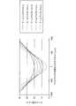
以下に好ましい入射角αの設定方法についてさらに詳細に説明する。光スイッチ装置1000の透過率のスペクトル帯域とビーム径との関係についてさらに詳述する。まず、信号光L1aの光分散方向(方向D1)のビーム半径ωh3(図1参照)が小さい場合、信号光L1aのビームウェストと光スイッチ素子50との光伝搬方向(z軸方向)における位置ずれが発生すると、光スイッチ装置1000の挿入損失が増加(透過率が低下)するとともに、透過率のスペクトル帯域が狭くなる。ここで、帯域の性能を示す指標として、2ω/dがある。dは信号光L1a、L1b、L1cに割り当てられた光スイッチ素子50の分散方向の幅を示し、ωは光スイッチ素子50近傍のビームウェストにおけるビーム半径を示す。図5(a)に示すように、2ω/dが小さいほど(d/ωが大きいほど)、透過率の0.5dB帯域が広くなり、好ましい。なお、0.5dB帯域とは、図5(b)に示すように、光の周波数を横軸とした透過率スペクトルにおいて、スペクトルのピークから0.5dBだけ透過率が低下する帯域を意味する。A preferable method for setting the incident angle α will be described in more detail below. The relationship between the spectral band of the transmittance of the
また、図6に示すように、信号光L1aのビームウェストと光スイッチ素子50との光伝搬方向における位置ずれ(光スイッチ素子50のビームウェスト位置からのオフセット)が大きいほど、光スイッチ素子50での信号光L1a、L1b、L1cのビーム半径が大きくなる(ビームが広がってしまう)。特に、ビームウェスト半径が小さいビームであるほどそのビーム半径の広がりの程度が大きい。なお、ビームウェストの位置とは、ビーム径が最小となるときのビーム形状の中心位置とする。 Further, as shown in FIG. 6, the larger the positional shift in the light propagation direction between the beam waist of the signal light L1a and the optical switch element 50 (offset from the beam waist position of the optical switch element 50), the greater the
図7は、計算による2ω/dと0.5dB帯域との関係を示す図である。なお、dは100μmとしている。図7に示すように、2ω/dと0.5dB帯域とは凡そ負の傾きを持つ線形の関係となり、BW=−39.745×2ω/d+50となる。BWは0.5dB帯域を示す。また、矢印はそれぞれωが12μm、14μm、22μmの位置を示している。 FIG. 7 is a diagram illustrating the relationship between the calculated 2ω / d and the 0.5 dB band. Note that d is 100 μm. As shown in FIG. 7, the 2ω / d and 0.5 dB bands have a linear relationship with a negative slope, and BW = −39.745 × 2ω / d + 50. BW indicates a 0.5 dB band. The arrows indicate the positions at which ω is 12 μm, 14 μm, and 22 μm, respectively.
たとえば、WDM信号において、信号光を配置するグリッドの間隔を光の周波数で50GHzとする場合、0.5dB帯域はおよそ35GHz以上であることが好ましい。図7より、光伝搬方向における位置ずれのオフセットによる0.5dB帯域の減少量を1GHz以下としたい場合を考える。たとえば、0.5dB帯域が36GHzから35GHzとなる場合、2ω/dは、0.359から0.384になる。すなわち、オフセットによるビーム半径ωのビームウェスト半径からの増加率を7%以下とすればよい。同様にして、減少量を2GHz以下としたい場合は、ビーム半径ωの増加率を14%以下とすればよく、減少量を3GHz以下としたい場合は、ビーム半径ωの増加率を20%以下とすればよいことがわかる。なお、このような増加率の設定は、回折格子30の配置により入射角αを調整することで実現することができる。 For example, in a WDM signal, when the interval between grids where signal light is arranged is 50 GHz in terms of light frequency, the 0.5 dB band is preferably about 35 GHz or more. From FIG. 7, a case is considered in which the amount of reduction in the 0.5 dB band due to the offset of the positional deviation in the light propagation direction is to be 1 GHz or less. For example, when the 0.5 dB band is from 36 GHz to 35 GHz, 2ω / d is from 0.359 to 0.384. That is, the increase rate of the beam radius ω due to the offset from the beam waist radius may be set to 7% or less. Similarly, when the reduction amount is 2 GHz or less, the increase rate of the beam radius ω may be 14% or less, and when the reduction amount is 3 GHz or less, the increase rate of the beam radius ω is 20% or less. You can see that Note that such an increase rate can be set by adjusting the incident angle α according to the arrangement of the
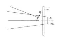
図8は、オフセットとビーム半径の増加率との関係を示す図である。縦軸の破線は、ビーム半径の増加量が7%、14%、20%の位置をそれぞれ示している。図9は、計算により求めた、光入出力ポート10において集光レンズ40の光軸40aと一致する光ファイバポート13から入力される光の光スイッチ素子50近傍におけるビームウェストの位置I2と、光入出力ポート10において集光レンズ40の光軸40aから最もはずれた光ファイバポート11または15から入力される光の光スイッチ素子50近傍におけるビームウェストの位置I1を分散方向にプロットした図である。図9が示すように、集光レンズ40の光学収差により光学軸に近いポートと光学軸から離れたポートではビームウェスト位置が互いにz方向(光軸方向)で400μm程だけずれる場合がある。図10が示すように、このような光軸40a上のポートからの光のビームウェストBaと光軸40aから最も離れたポートからの光のビームウェストBbとの400μmのずれの中間地点に光スイッチ素子50を配置すると、各ビームウェストに対するオフセットは200μmとなる。図8から、オフセットが200μm以下である場合、光スイッチ素子50近傍でのビームウェスト半径が16.2μm以上であればオフセットによるビーム半径ωのビームウェスト半径からの増加率を7%以下とすることができ、0.5dB帯域の減少量を1GHz以下とできる。同様に、ビームウェスト半径が13.6μm以上であればビーム半径ωの増加率を14%以下とすることができ、0.5dB帯域の減少量を2GHz以下とでき、ビームウェスト半径が12μm以上である12.2μm以上であればビーム半径ωの増加率を20%以下とすることができ、0.5dB帯域の減少量を3GHz以下とできることがわかる。なお、このようなビームウェスト半径の設定は、回折格子30の配置により入射角αを調整することで実現することができる。 FIG. 8 is a diagram showing the relationship between the offset and the increase rate of the beam radius. The broken lines on the vertical axis indicate the positions where the increase amount of the beam radius is 7%, 14%, and 20%, respectively. FIG. 9 shows the position I2 of the beam waist in the vicinity of the
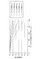
図11は、オフセットと、結合効率との関係を示す図である。図11ではオフセットが0μmの場合を基準として、オフセットが生じたときの結合効率の低下(すなわち、光スイッチ装置の挿入損失の増加)を示している。ここで、光スイッチ装置の典型的な挿入損失は10dB以下であることを考慮すると、オフセットによる挿入損失の増加は0.5dB以下とすることが望ましい。この点から、図11に示すように、オフセットが200μm以下である場合、光スイッチ素子50近傍でのビームウェスト半径を12μm以上とすれば、オフセットによる挿入損失の増加を0.5dB以下とすることができる。なお、このようなビームウェスト径の設定は、回折格子30の配置により入射角αを調整することで実現することができる。 FIG. 11 is a diagram illustrating the relationship between offset and coupling efficiency. FIG. 11 shows a decrease in coupling efficiency (that is, an increase in insertion loss of the optical switch device) when the offset occurs, with the offset being 0 μm as a reference. Here, considering that the typical insertion loss of the optical switch device is 10 dB or less, it is desirable that the increase of the insertion loss due to the offset is 0.5 dB or less. From this point, as shown in FIG. 11, when the offset is 200 μm or less, if the beam waist radius in the vicinity of the
以上のように、オフセットによるビーム半径ωのビームウェスト半径からの増加率が20%以下となるように入射角αを調整することにより、0.5dB帯域の減少量を3GHz以下とすることができ、増加率が14%以下となるように入射角αを調整することにより、0.5dB帯域の減少量を2GHz以下とすることができ、増加率が7%以下となるように入射角αを設定することにより、0.5dB帯域の減少量を1GHz以下とすることができる。
また、光スイッチ素子50近傍でのビームウェスト半径を12μm以上となるように入射角αを設定することにより、オフセットによる挿入損失の増加を0.5dB以下とすることができる。
なお、入射角αをリトロー角θLとよりも小さくし、その差を大きくすることで、ビームウェスト半径をより大きくでき、オフセットによるビーム半径ωのビームウェスト半径からの増加率を小さく抑えることができる。As described above, the amount of decrease in the 0.5 dB band can be reduced to 3 GHz or less by adjusting the incident angle α so that the increase rate of the beam radius ω due to the offset from the beam waist radius is 20% or less. By adjusting the incident angle α so that the increase rate is 14% or less, the amount of decrease in the 0.5 dB band can be 2 GHz or less, and the incident angle α is set so that the increase rate is 7% or less. By setting, the reduction amount of the 0.5 dB band can be made 1 GHz or less.
Also, by setting the incident angle α so that the beam waist radius in the vicinity of the
Note that the incident angle α smaller than the Littrow angle thetaL, by increasing the difference, the beam can increase the waist radius, it is possible to reduce the rate of increase from the beam waist radius of the beam radius ω due to the offset it can.
本実施形態においては、光分散方向におけるビーム径が大きくなるため、挿入損失の増大と帯域の低減を抑制できるという効果も得られる。
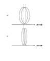
本効果について、さらに詳細に説明する。まず、光分散方向における光スイッチ素子50近傍でのビームウェスト半径について説明する。光分散方向における光スイッチ素子50近傍でのビームウェスト半径が小さいと、光スイッチ装置1000の挿入損失が大きくなりやすく、かつ0.5dB帯域が劣化しやすい。図12は、光入出力ポート10の異なる2つのポートから入力した各光の光スイッチ素子50上でのビームの状態を示しており、図12(a)は光スイッチ素子50上での光分散方向におけるビーム半径が大きい場合を示しており、図12(b)は光スイッチ素子50上でのビーム半径が小さい場合を示している。図12に示すように、2つのビームの光分散方向(y軸方向)における位置ずれ量が同じであっても、図12(b)の場合のように光分散方向におけるビーム半径が小さいと、2つのビームの重なり積分が小さくなるため、結合効率が低下して挿入損失が増加する。また、帯域が低減しやすい。In this embodiment, since the beam diameter in the light dispersion direction is increased, an effect of suppressing an increase in insertion loss and a reduction in bandwidth can be obtained.
This effect will be described in more detail. First, the beam waist radius near the
図13は、ビームウェストと光スイッチ素子との分散方向における位置ずれと、結合効率との関係を示す図である。図13より、ビームウェスト半径(ωh3、図1参照)が小さいと、光スイッチ素子50のy軸方向における位置ずれに応じて結合効率が低下して挿入損失が増大しやすい。FIG. 13 is a diagram showing the relationship between the displacement in the dispersion direction between the beam waist and the optical switch element and the coupling efficiency. From FIG. 13, when the beam waist radius (ωh3 , see FIG. 1) is small, the coupling efficiency is lowered and the insertion loss is likely to increase according to the positional deviation of the
これに対して、光スイッチ装置1000では、入射角αをリトロー角θLより小さくしているので、光分散方向におけるビーム径が大きくなるため、挿入損失の増大と帯域の低減を抑制できる。これにより、光スイッチ装置1000の作製時における光スイッチ素子50の位置ずれに対する光スイッチ装置1000の透過率のスペクトル帯域のトレランスが高くなる。その結果、光スイッチ装置1000は製造性高く小型化できる。In contrast, the
図14は、比較例と実施例の光スイッチ装置の0.5dB帯域の波長依存性の測定結果を示す図である。実施例の光スイッチ装置は光スイッチ装置1000の構成を有し、入射角αを、リトロー角である48.3°から2.3°だけ小さくした46°としたものである。比較例の光スイッチ装置は光スイッチ装置1000の構成を有するが、入射角αを、リトロー角である48.3°としたものである。なお、測定した波長帯域は1529nm〜1565nmである。 FIG. 14 is a diagram illustrating measurement results of wavelength dependence in the 0.5 dB band of the optical switch devices of the comparative example and the example. The optical switch device of the embodiment has the configuration of the
光スイッチ素子近傍での光分散方向のビームウェスト半径については、上記波長帯の最短波長において、比較例で14μm、実施例で17μmであった。また、上記波長帯の最長波長において、比較例で18μm、実施例で22μmであった。また、上記波長帯域において光スイッチ素子上で光が入射される50GHz gridの領域の幅は、比較例で100μmであり、実施例で113μmであった。また、比較例では、最短波長から最長波長までの光が入射される領域(両側のビームの端部から端部までの領域)の幅は、有効エリアの幅88%であり、実施例では有効エリアの幅95%であった。また、上記波長帯の最短波長において、2ω/dの値は、比較例で0.30、実施例で0.28であった。 The beam waist radius in the light dispersion direction in the vicinity of the optical switch element was 14 μm in the comparative example and 17 μm in the example at the shortest wavelength in the wavelength band. Moreover, in the longest wavelength of the said wavelength range, it was 18 micrometers in the comparative example and 22 micrometers in the Example. Further, the width of the 50 GHz grid region in which light is incident on the optical switch element in the wavelength band was 100 μm in the comparative example and 113 μm in the example. In the comparative example, the width of the region where light from the shortest wavelength to the longest wavelength is incident (the region from the end to the end of the beams on both sides) is 88% of the effective area, which is effective in the embodiment. The area width was 95%. Further, at the shortest wavelength in the above wavelength band, the value of 2ω / d was 0.30 in the comparative example and 0.28 in the example.
図14(a)に示す比較例では、短波長側の0.5dB帯域が約3GHz低下したが、図14(a)に示す実施例では、短波長側の0.5dB帯域の低下が約2GHzに改善された。また、比較例では光スイッチ素子の有効エリアの88%を使用できたが、実施例では有効エリアの90%以上である95%を使用できた。 In the comparative example shown in FIG. 14A, the 0.5 dB band on the short wavelength side is reduced by about 3 GHz. However, in the example shown in FIG. 14A, the reduction in the 0.5 dB band on the short wavelength side is about 2 GHz. Improved. In the comparative example, 88% of the effective area of the optical switch element could be used, but in the example, 95%, which is 90% or more of the effective area, could be used.
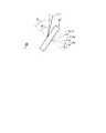
(実施形態2)
図15、16は、本発明の実施形態2に係る光スイッチ装置の模式的な構成図である。この光スイッチ装置1000Aは、実施形態1に係る光スイッチ装置1000の構成において、光スイッチ素子50を光スイッチ素子50Aに置き換え、回折格子30の配置を変更したものである。光スイッチ装置1000Aのその他の構成や基本的な動作は光スイッチ装置1000と同様であるので、説明を省略する。(Embodiment 2)
15 and 16 are schematic configuration diagrams of the optical switch device according to the second embodiment of the present invention. This
回折格子30への信号光L1の入射角について図を参照して説明する。図17に示すように、信号光L1は、破線で示す回折格子30の法線に対して入射角α1で入射する。信号光L1a、L1b、L1cはその波長に応じた回折角で回折される。たとえば信号光L1aの回折角はβ1である。 An incident angle of the signal light L1 to the
ここで、実施形態2に係る光スイッチ装置1000Aでは、回折格子30の入射角α1とリトロー角θLとが異なるように配置されている。ここで、入射角αとリトロー角θLとが異なるとは、たとえば、両者の差が1°よりも大きいことを意味する。具体的には、入射角α1がリトロー角θLよりも大きい。なお、実施形態2では、リトロー角θLを、入射する信号光L1a、L1b、L1cが形成する波長帯域の中心波長である信号光L1aの波長の光に対して定義する。Here, the
光スイッチ装置1000Aは、回折格子30への信号光L1(L1a)の入射角α1がリトロー角θLよりも大きいことにより、y方向の小型化ができる。その理由を以下に説明する。
図18は、光スイッチ素子と信号光のビームとを示す図である。図18(a)に示すように、光スイッチ素子50Aは光スイッチ素子50よりも小型のものであり、光スイッチ素子50Aの有効エリア50Aaの幅は、光スイッチ素子50の有効エリア50aの幅より狭くなっている。したがって、光スイッチ装置1000のように信号光L1(L1a)の入射角αがリトロー角θLよりも小さい場合、光スイッチ素子50を用いた場合は信号光L1a、L1b、L1cのいずれも有効エリア50aに入射するが、光スイッチ素子50Aを用いた場合は信号光L1b、L1cは有効エリア50Aaに入射しないこととなり、光スイッチングを行うことができない。FIG. 18 is a diagram showing an optical switch element and a beam of signal light. As shown in FIG. 18A, the
そこで、本発明者は、光スイッチ装置を設計するにあたり、回折格子への光の入射角をリトロー角とは異なるように回折格子を配置することで、回折された光のビームの特性を調整し、光スイッチ装置の小型化が実現される設計とできることに想到した。 Therefore, when designing the optical switch device, the present inventor adjusts the characteristics of the diffracted light beam by arranging the diffraction grating so that the incident angle of the light to the diffraction grating is different from the Littrow angle. The inventors have come up with the idea that the optical switch device can be designed to be miniaturized.
光スイッチ装置1000Aでは、信号光L1(L1a)の入射角α1がリトロー角θLよりも大きい。図4を参照して説明したように、入射角α1を大きくすると回折角β1が小さくなり、信号光L1a(および信号光L1b、L1c)のy軸方向での分散も小さくなる。その結果、図18(b)に示すように、信号光L1a、L1b、L1cのいずれも有効エリア50Aaに入射し、いずれの信号光に対しても光スイッチングを行うことができる。In the
すなわち、光スイッチ装置1000Aは、回折格子30への信号光L1(L1a)の入射角α1がリトロー角θLより大きいことにより、より小型の光スイッチ素子50Aを用いることができるので、装置全体を小型化できる。That is, the
なお、入射角α1は、許容される挿入損失や使用波長帯域などを考慮して、使用する光スイッチ素子50Aの有効エリア50Aaの幅に応じて設定し、このような入射角α1となるように回折格子30を配置することで実現することができる。 The incident angle α1 is set in accordance with the width of the effective area 50Aa of the
(実施形態3)
図19、20は、本発明の実施形態3に係る光スイッチ装置の模式的な構成図である。この光スイッチ装置1000Bは、実施形態2に係る光スイッチ装置1000Aの構成において、光スイッチ素子50Aを光スイッチ素子50Bに置き換え、制御部60を制御部60Bに置き換えたものである。光スイッチ装置1000Bのその他の構成や基本的な動作は光スイッチ装置1000Aと同様であるので、説明を省略する。(Embodiment 3)
19 and 20 are schematic configuration diagrams of an optical switch device according to
光スイッチ素子50Bは、光分散方向(y軸方向)に沿って離散的に配列された複数の操作素子であるMEMSミラー50Ba、50Bb、50Bcを有している。 The
制御部60Bは、光スイッチ素子50Bの各MEMSミラー50Ba、50Bb、50Bcに電圧信号を印加し、ミラー面の角度を制御する。これにより、光スイッチ素子50Bでは、MEMSミラー50Ba、50Bb、50Bcのそれぞれに信号光L1a、L1b、L1cのそれぞれが入射されると、各MEMSミラー50Ba、50Bb、50Bcはミラー面の角度が制御されて、各信号光L1b、L1a、L1cを、各信号光の波長に応じた所定の角度で反射させる。 The
この光スイッチ装置1000Bは、光スイッチ装置1000Aと同様に、回折格子30への信号光L1(L1a)の入射角α1がリトロー角θLよりも大きいことにより、小型化できる。The
図21は、光スイッチ素子と信号光のビームとを示す図である。図21(a)に示すように、MEMSミラー50Ba、50Bb、50Bcはy軸方向で離散的に配列されている。したがって、回折格子30への信号光L1(L1a)の入射角によっては、信号光L1b、L1cはMEMSミラー50Bb、50Bcに入射しないこととなり、光スイッチングを行うことができない。 FIG. 21 is a diagram illustrating an optical switch element and a beam of signal light. As shown in FIG. 21A, the MEMS mirrors 50Ba, 50Bb, and 50Bc are discretely arranged in the y-axis direction. Therefore, depending on the incident angle of the signal light L1 (L1a) to the
これに対して、光スイッチ装置1000Bでは、信号光L1(L1a)の入射角α1がリトロー角θLよりも大きいので、信号光L1a(および信号光L1b、L1c)のy軸方向での分散も小さくなる。その結果、図21(b)に示すように、信号光L1a、L1b、L1cのいずれも、対応するMEMSミラー50Ba、50Bb、50Bcに入射し、いずれの信号光に対しても光スイッチングを行うことができる。In contrast, the
すなわち、光スイッチ装置1000Bは、回折格子30への信号光L1(L1a)の入射角α1がリトロー角θLよりも大きいことにより、より小型の光スイッチ素子50Bを用いることができるので、装置全体を小型化できる。That is, the
なお、入射角α1は、許容される挿入損失や使用波長帯域などを考慮して、WDM信号光に含まれる各信号光が分光されて、光スイッチ素子の各MEMSミラーに到達するように設定し、このような入射角α1となるように回折格子30を配置することで実現することができる。 The incident angle α1 is set so that each signal light included in the WDM signal light is dispersed and reaches each MEMS mirror of the optical switch element in consideration of an allowable insertion loss, a used wavelength band, and the like. This can be realized by arranging the
(実施形態4)
図22は、本発明の実施形態4に係る光源装置の模式的な構成図である。この光源装置1000Cは、実施形態3に係る光スイッチ装置1000Bの構成において、光入出力ポート10を光出力ポート10Cに置き換え、光スイッチ素子50Bを光源アレイ50Cに置き換え、制御部60Bを制御部60Cに置き換えたものであり、WDMレーザ光源として機能する。光源装置1000Cのその他の構成は光スイッチ装置1000Bと同様であるので、説明を省略する。(Embodiment 4)
FIG. 22 is a schematic configuration diagram of a light source device according to
光出力ポート10Cは、光ファイバからなる光ファイバポート11〜15と、コリメート部16Cとを備えている。光ファイバポート11〜15は、外部に光を出力するものである。コリメート部16Cは、光ファイバポート11に対応して設けられたコリメータレンズを備えている。このコリメータレンズは、入力された平行光を光ファイバポート11に集光して結合させる機能を有する。なお、コリメート部16Cは、コリメータレンズの代わりにコリメート機能を有する光導波路を備えていてもよい。 The
光源アレイ50Cは、光分散方向(y軸方向)に沿って離散的に配列された複数の光源である半導体レーザ素子50Ca、50Cb、50Ccを有している。半導体レーザ素子50Ca、50Cb、50Ccは、駆動電力を供給することにより、互いに波長が異なるレーザ光L2a、L2b、L2cを出力するように構成されている。レーザ光L2a、L2b、L2cの波長については、レーザ光L2cが最も長波長であり、レーザ光L2bが最も短波長であり、レーザ光L2aがその中央の波長であるとする。 The
制御部60Cは、光源アレイ50Cに駆動電力を供給するように構成されている。 The
つぎに、光源装置1000Cの動作について説明する。制御部60Cが光源アレイ50Cに駆動電力を供給すると、半導体レーザ素子50Ca、50Cb、50Ccはそれぞれレーザ光L2a、L2b、L2cを出力する。レーザ光L2a、L2b、L2cはx軸方向に長軸を有する楕円形のビームとして出力される。 Next, the operation of the
集光レンズ40は、レーザ光L2a、L2b、L2cを回折格子30に集光させる。集光後のレーザ光L2a、L2b、L2cはy軸方向に長軸を有する楕円形のビームとなる。 The condensing
回折格子30は、レーザ光L2a、L2b、L2cを所定の回折角で回折する。ここで、図23に示すように、回折格子30は、レーザ光L2aがリトロー角θLとは異なる入射角で入射し、かつ各レーザ光L2a、L2b、L2cが同じ回折角β3で出射するように配置されている。なお、実施形態3では、リトロー角θLを、レーザ光L2a、L2b、L2cが形成する波長帯域(使用波長帯域)の中心波長であるレーザ光L2aの波長の光に対して定義する。レーザ光L2aの波長が使用波長帯域の中心波長からずれている場合には、使用波長帯域の中心波長の光に対してリトロー角θLを定義する。たとえば、レーザ光L2aの入射角α3はリトロー角θLよりも大きい。その結果、3つのレーザ光L2a、L2b、L2cは合波されて1つのWDMレーザ光L2となる。The
アナモルフィック光学系20は、WDMレーザ光L2の入力を受け付け、そのビーム形状を方向D1の方向に縮小して略円形とする。その後、WDMレーザ光L2はコリメート部16Cのコリメータレンズに入力する。このコリメータレンズは、WDMレーザ光L2を集光し、光ファイバポート11に結合させる。光ファイバポート11は結合されたWDMレーザ光L2を外部に出力する。以上のようにして、この光源装置1000Cは、WDMレーザ光源として機能する。 The anamorphic
この光源装置1000Cは、回折格子30へのレーザ光L2aの入射角α3がリトロー角θLよりも大きいことにより、半導体レーザ素子50Ca、50Cb、50Ccの離間間隔が小さい小型の光源アレイ50Cを用いることができるので、装置全体を小型化できる。また、回折格子30が、各レーザ光L2a、L2b、L2cが同じ回折角β3で出射するように配置されているので、確実にWDMレーザ光L2を生成することができる。なお、入射角α3は、半導体レーザ素子50Ca、50Cb、50Ccの離間間隔に応じて適宜設定することができる。The
なお、光源アレイにおける複数の光源として、円形のビーム形状の光を出力するものを用いた場合は、アナモルフィック光学系を使用しなくてもよい。 When a light source that outputs circular beam-shaped light is used as the plurality of light sources in the light source array, the anamorphic optical system may not be used.
また、上記実施形態では、集光レンズ系である集光レンズ40は単レンズで構成されているが、本発明はこれに限らず、複数のレンズで構成されている集光レンズ系を用いても良い。また、集光レンズ系として、シリンドリカルレンズを用いてもよい。 Moreover, in the said embodiment, although the condensing
また、上記実施形態では、光スイッチ装置は1×4光スイッチであるが、本発明では光が入出力するポートの数は特に限定されず、N×M光スイッチ(N、Mは任意の整数)であればよい。また、たとえば光スイッチ装置1000の構成において、光ファイバポート12、13、14、15のいずれかから信号光を入力させて、Comポートとしての光ファイバポート11から出力させるように光スイッチ装置1000を動作させてもよい。これによって、光スイッチ装置1000を4×1光スイッチとして使用することができる。 In the above embodiment, the optical switch device is a 1 × 4 optical switch. However, in the present invention, the number of ports through which light is input and output is not particularly limited, and N × M optical switches (N and M are arbitrary integers). ). Further, for example, in the configuration of the
また、上記実施形態では、光操作装置を光スイッチ装置として説明してきたが、光操作素子としての光スイッチ素子を他の光操作機能を有する光操作素子に置き換えることで、例えば光フィルタや分散補償器等の光操作装置としても利用することができる。 In the above embodiment, the optical manipulation device has been described as an optical switching device. However, by replacing the optical switching device as the optical manipulation device with an optical manipulation device having another optical manipulation function, for example, an optical filter or dispersion compensation It can also be used as an optical operation device such as a container.
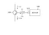
光フィルタは、入力されたWDM信号光に含まれる特定の信号光の強度を減衰させたり、入力されたWDM信号光に含まれる信号光毎に異なる量の光減衰を与えて出力する光操作装置である。光フィルタは、たとえば光スイッチ装置1000の光スイッチ素子50を、光操作素子を有する光減衰部に置き換えることで実現できる。光減衰部はたとえばSLMで構成できる。したがって、光フィルタは、光入力ポートと光出力ポートと、アナモルフィック光学系と、回折格子と、集光レンズ系と、光減衰部とをこの順番に配置して構成することができる。光フィルタの機能は、光入力ポートから入力されたWDM信号光が回折格子によって分光され、光減衰部に入力された信号光のうち、強度を減衰した信号光を光出力ポートに、強度が減衰するような入射角度で入射するようにスイッチするように制御することで実現される。上記光入力ポートと光出力ポートは必ずしも、別のポートである必要はなく、1つの光入出力ポートで光入力ポートと光出力ポートを兼ねてもよい。その場合は、図24に示すように、光フィルタ1200の1つの光入出力ポート1210の手前に光サーキュレータ1220を配置する構成とすることが好ましい。この構成によって、光サーキュレータ1220を介して、信号光L1を光フィルタ1200の1つの光入出力ポート1210に入力して、強度を減衰させた信号光L1aを取り出すことができる。 The optical filter attenuates the intensity of the specific signal light included in the input WDM signal light, or outputs a different amount of optical attenuation for each signal light included in the input WDM signal light. It is. The optical filter can be realized, for example, by replacing the
分散補償器は、入力された光の各波長成分の遅延時間を制御することで各波長成分の波長分散を補償する機能を持つ光操作装置である。分散補償器は、たとえば光スイッチ装置1000の光スイッチ素子50を、光操作素子を有する分散補償部に置き換えることで実現できる。分散補償部はたとえば光操作素子としてのSLMで構成できる。したがって、分散補償部は、光入力ポートと光出力ポートと、アナモルフィック光学系と、回折格子と、集光レンズ系と、分散補償部とをこの順番に配置して構成することができる。分散補償部の機能は、光入力ポートから入力された光が回折格子によって分光され、分散補償部に入力された各波長成分に、異なる遅延時間を与えるように制御することで実現される。分散補償器の場合も、光フィルタと同様に、上記光入力ポートと光出力ポートは必ずしも、別のポートである必要はなく、1つの光入出力ポートで光入力ポートと光出力ポートを兼ねてもよい。その場合は、図24と同様に、光入出力ポートの手前に光サーキュレータを配置することで出力光を取り出すことができる。 The dispersion compensator is an optical manipulation device having a function of compensating the chromatic dispersion of each wavelength component by controlling the delay time of each wavelength component of input light. The dispersion compensator can be realized, for example, by replacing the
また、上実施形態では、回折格子30は一つの回折格子で構成されているが、これに換えて複数の回折格子からなる回折格子ユニットを用いてもよい。たとえば、図25のように、2つの透過型の回折格子30Aa、30Abで構成される回折格子ユニット30Aの場合、回折格子ユニット30Aにおける信号光L1の入射角α4と回折角β4とは図示した角度となる。 Further, in the above embodiment, the
ところで、本発明において、回折格子への入射角αをリトロー角θLよりも大きくするか、小さくするかは、これを適用する光操作装置または光源装置に対してどの方向での小型化が必要かによって選択できる。以下では光操作装置の場合について説明するが、光源装置に対しても同様の理由で選択を行うことができる。By the way, in the present invention, whether to make the incident angle α to the diffraction grating larger or smaller than the Littrow angle θL is required to be smaller in any direction with respect to the optical operation device or the light source device to which the incident angle α is applied. You can choose depending on what. In the following, the case of the optical operation device will be described, but the selection can be made for the light source device for the same reason.
まず、yz平面方向またはx方向の小型化を行うため、集光レンズの焦点距離を短くする場合について説明する。焦点距離を短くすると、集光レンズ近傍でのx方向でのビーム径が小さくなるため、x方向での小型化をすることができる。なお、集光レンズの焦点距離を短くしたことにより、回折格子を入射角=リトロー角で配置したときに、光スイッチ素子(光操作素子)近傍におけるビーム径が小さくなることにより光操作装置の特性が劣化する場合は、入射角をリトロー角よりも小さくする。
逆に、信号光の光スイッチ素子(光操作素子)への入射領域(y方向における幅)を狭くし、y方向の小型化を行いたい場合は入射角をリトロー角よりも大きくすればよい。First, a case where the focal length of the condenser lens is shortened in order to reduce the size in the yz plane direction or the x direction will be described. When the focal length is shortened, the beam diameter in the x direction in the vicinity of the condensing lens is reduced, so that the size in the x direction can be reduced. In addition, by shortening the focal length of the condensing lens, when the diffraction grating is arranged at an incident angle = Littrow angle, the beam diameter in the vicinity of the optical switch element (light manipulation element) becomes small, and the characteristics of the light manipulation device Is deteriorated, the incident angle is made smaller than the Littrow angle.
On the other hand, if the incident area (width in the y direction) of the signal light to the optical switch element (optical manipulation element) is narrowed and the size in the y direction is desired to be reduced, the incident angle may be made larger than the Littrow angle.
また、上記実施形態により本発明が限定されるものではない。上述した各構成要素を適宜組み合わせて構成したものも本発明に含まれる。また、さらなる効果や変形例は、当業者によって容易に導き出すことができる。よって、本発明のより広範な態様は、上記の実施形態に限定されるものではなく、様々な変更が可能である。 Further, the present invention is not limited by the above embodiment. What was comprised combining each component mentioned above suitably is also contained in this invention. Further effects and modifications can be easily derived by those skilled in the art. Therefore, the broader aspect of the present invention is not limited to the above-described embodiment, and various modifications can be made.
10、1210 光入出力ポート
10C 光出力ポート
11、12、13、14、15 光ファイバポート
16、16C コリメート部
20 アナモルフィック光学系
30、30Aa、30Ab 回折格子
30A 回折格子ユニット
40 集光レンズ
40a 光軸
50、50A、50B 光スイッチ素子
50a、50Aa 有効エリア
50Ba、50Bb、50Bc MEMSミラー
50C 光源アレイ
50Ca、50Cb、50Cc 半導体レーザ素子
60、60B、60C 制御部
1000、1000A、1000B 光スイッチ装置
1000C 光源装置
1200 光フィルタ
1220 光サーキュレータ
B1、B2、B3、B31、B32、B33 ビーム
Ba、Bb ビームウェスト
D1、D2 方向
I1、I2 位置
L1、L1a、L1b、L1c 信号光
L2 WDMレーザ光
L2a、L2b、L2c レーザ光DESCRIPTION OF
Claims (11)
Translated fromJapanese前記光入出力ポートのいずれかのポートから入力した光を前記光入出力ポートのいずれかのポートに向けて出力するための光操作素子と、
前記光入出力ポートと前記光操作素子との間に配置され、前記光入出力ポートと前記光操作素子とを光学的に結合させる集光レンズ系と、
前記光入出力ポートと前記集光レンズ系との間に配置され、前記ポートから入力した光を光分散方向に分光する透過型の回折格子と、
を備え、
前記回折格子は、前記光入出力ポートから入力した光の入射角とリトロー角とが異なるように配置されている
ことを特徴とする光操作装置。An optical input / output port having at least one port through which light is input from the outside or outputs light to the outside;
A light manipulation element for outputting light input from any one of the light input / output ports toward any port of the light input / output port;
A condensing lens system that is disposed between the light input / output port and the light manipulation element and optically couples the light input / output port and the light manipulation element;
A transmissive diffraction grating that is disposed between the light input / output port and the condenser lens system and separates light input from the port in a light dispersion direction;
With
The optical operation device, wherein the diffraction grating is arranged so that an incident angle and a Littrow angle of light input from the light input / output port are different.
離散的に配列された、互いに波長が異なる光を出力する複数の光源と、
前記光出力ポートと前記複数の光源との間に配置され、前記光出力ポートと前記複数の光源とを光学的に結合させる集光レンズ系と、
前記光出力ポートと前記集光レンズ系との間に配置され、前記複数の光源から出力された各光を前記複数の光源の配列方向である光分散方向で分光する透過型の回折格子と、
を備え、
前記回折格子は、前記複数の光源から入力した各光がリトロー角とは異なる入射角で入射し、かつ前記各光が同じ回折角で出射するように配置されている
ことを特徴とする光源装置。An optical output port having a port for outputting light to the outside;
A plurality of light sources that output discretely arranged light having different wavelengths,
A condensing lens system that is disposed between the light output port and the plurality of light sources, and optically couples the light output port and the plurality of light sources;
A transmissive diffraction grating that is disposed between the light output port and the condenser lens system and separates each light output from the plurality of light sources in a light dispersion direction that is an arrangement direction of the plurality of light sources;
With
The diffraction grating is arranged so that each light input from the plurality of light sources is incident at an incident angle different from a Littrow angle, and the respective lights are emitted at the same diffraction angle. .
Priority Applications (1)
| Application Number | Priority Date | Filing Date | Title |
|---|---|---|---|
| JP2016025248AJP2017142465A (en) | 2016-02-12 | 2016-02-12 | Optical operation device and light source device |
Applications Claiming Priority (1)
| Application Number | Priority Date | Filing Date | Title |
|---|---|---|---|
| JP2016025248AJP2017142465A (en) | 2016-02-12 | 2016-02-12 | Optical operation device and light source device |
Publications (1)
| Publication Number | Publication Date |
|---|---|
| JP2017142465Atrue JP2017142465A (en) | 2017-08-17 |
Family
ID=59629044
Family Applications (1)
| Application Number | Title | Priority Date | Filing Date |
|---|---|---|---|
| JP2016025248APendingJP2017142465A (en) | 2016-02-12 | 2016-02-12 | Optical operation device and light source device |
Country Status (1)
| Country | Link |
|---|---|
| JP (1) | JP2017142465A (en) |
Citations (11)
| Publication number | Priority date | Publication date | Assignee | Title |
|---|---|---|---|---|
| JPH11183249A (en)* | 1997-12-24 | 1999-07-09 | Ando Electric Co Ltd | Spectroscope |
| WO2004081620A1 (en)* | 2003-03-13 | 2004-09-23 | Asahi Glass Company Limited | Diffraction element and optical device |
| US20080291950A1 (en)* | 2003-02-25 | 2008-11-27 | Finisar Corporation | Optical beam steering for tunable laser applications |
| JP2009121986A (en)* | 2007-11-15 | 2009-06-04 | Omron Corp | Spectral apparatus |
| JP2012203136A (en)* | 2011-03-24 | 2012-10-22 | Olympus Corp | Wavelength selecting switch |
| JP2013521666A (en)* | 2010-03-05 | 2013-06-10 | テラダイオード,インコーポレーテッド | Wavelength beam combining system and method |
| JP2014199296A (en)* | 2013-03-29 | 2014-10-23 | 古河電気工業株式会社 | Optical operation device |
| JP2015026860A (en)* | 2006-03-09 | 2015-02-05 | インフェイズ テクノロジーズ インコーポレイテッド | External cavity laser |
| JP2015028528A (en)* | 2013-07-30 | 2015-02-12 | キヤノン株式会社 | Transmission diffractive optical element and measuring apparatus |
| JP2015206599A (en)* | 2014-04-17 | 2015-11-19 | 国立研究開発法人日本原子力研究開発機構 | polarimeter and polarization angle expansion method |
| WO2015190127A1 (en)* | 2014-06-09 | 2015-12-17 | 古河電気工業株式会社 | Optical collimator array and optical switch device |
- 2016
- 2016-02-12JPJP2016025248Apatent/JP2017142465A/enactivePending
Patent Citations (11)
| Publication number | Priority date | Publication date | Assignee | Title |
|---|---|---|---|---|
| JPH11183249A (en)* | 1997-12-24 | 1999-07-09 | Ando Electric Co Ltd | Spectroscope |
| US20080291950A1 (en)* | 2003-02-25 | 2008-11-27 | Finisar Corporation | Optical beam steering for tunable laser applications |
| WO2004081620A1 (en)* | 2003-03-13 | 2004-09-23 | Asahi Glass Company Limited | Diffraction element and optical device |
| JP2015026860A (en)* | 2006-03-09 | 2015-02-05 | インフェイズ テクノロジーズ インコーポレイテッド | External cavity laser |
| JP2009121986A (en)* | 2007-11-15 | 2009-06-04 | Omron Corp | Spectral apparatus |
| JP2013521666A (en)* | 2010-03-05 | 2013-06-10 | テラダイオード,インコーポレーテッド | Wavelength beam combining system and method |
| JP2012203136A (en)* | 2011-03-24 | 2012-10-22 | Olympus Corp | Wavelength selecting switch |
| JP2014199296A (en)* | 2013-03-29 | 2014-10-23 | 古河電気工業株式会社 | Optical operation device |
| JP2015028528A (en)* | 2013-07-30 | 2015-02-12 | キヤノン株式会社 | Transmission diffractive optical element and measuring apparatus |
| JP2015206599A (en)* | 2014-04-17 | 2015-11-19 | 国立研究開発法人日本原子力研究開発機構 | polarimeter and polarization angle expansion method |
| WO2015190127A1 (en)* | 2014-06-09 | 2015-12-17 | 古河電気工業株式会社 | Optical collimator array and optical switch device |
Similar Documents
| Publication | Publication Date | Title |
|---|---|---|
| JP4860757B2 (en) | Dispersion compensator | |
| JP5692865B2 (en) | Wavelength cross-connect equipment | |
| JP5184637B2 (en) | Wavelength selective switch | |
| US10126556B2 (en) | Light operation device | |
| US20140072302A1 (en) | Optical switch | |
| US11067752B2 (en) | Reconfigurable optical add/drop multiplexer | |
| CN103969745B (en) | A kind of bandwidth levelling top-type optical filter based on DLP | |
| US11728919B2 (en) | Optical communications apparatus and wavelength selection method | |
| US12055763B2 (en) | Optical switching apparatus, redirection method, and reconfigurable optical add-drop multiplexer | |
| JP5855323B1 (en) | Optical collimator array and optical switch device | |
| JP2012185312A (en) | Optical switch device | |
| JP6251202B2 (en) | Wavelength selective switch | |
| WO2016056534A1 (en) | Wavelength-selective optical switch device | |
| WO2014157673A1 (en) | Wavelength-selective optical-switch device and method for controlling wavelength-selective optical-switch device | |
| JP6034319B2 (en) | Light switch | |
| JP6117158B2 (en) | Optical operation device and control method thereof | |
| CN112526678A (en) | Spectrum processing device and reconfigurable optical add-drop multiplexer | |
| JP5959466B2 (en) | Optical operation device | |
| CN116466436A (en) | Wavelength selective switch | |
| JP2017142465A (en) | Optical operation device and light source device | |
| US6947220B1 (en) | Devices for information processing in optical communications | |
| JP2005321480A (en) | Wavelength selection device | |
| CN116413862A (en) | Wavelength selective device, method of wavelength selection and ROADM | |
| JP5086317B2 (en) | Variable dispersion compensator | |
| JP2010237377A (en) | Prism, prism pair, and wavelength selection device including the prism pair |
Legal Events
| Date | Code | Title | Description |
|---|---|---|---|
| A621 | Written request for application examination | Free format text:JAPANESE INTERMEDIATE CODE: A621 Effective date:20170511 | |
| A977 | Report on retrieval | Free format text:JAPANESE INTERMEDIATE CODE: A971007 Effective date:20180312 | |
| A131 | Notification of reasons for refusal | Free format text:JAPANESE INTERMEDIATE CODE: A131 Effective date:20180320 | |
| A02 | Decision of refusal | Free format text:JAPANESE INTERMEDIATE CODE: A02 Effective date:20181009 |