JP2017129848A - Substrate holding device, drawing device, photomask inspection device, and manufacturing method of photomask - Google Patents
Substrate holding device, drawing device, photomask inspection device, and manufacturing method of photomaskDownload PDFInfo
- Publication number
- JP2017129848A JP2017129848AJP2016240885AJP2016240885AJP2017129848AJP 2017129848 AJP2017129848 AJP 2017129848AJP 2016240885 AJP2016240885 AJP 2016240885AJP 2016240885 AJP2016240885 AJP 2016240885AJP 2017129848 AJP2017129848 AJP 2017129848A
- Authority
- JP
- Japan
- Prior art keywords
- photomask
- substrate
- substrate holding
- holding device
- stage
- Prior art date
- Legal status (The legal status is an assumption and is not a legal conclusion. Google has not performed a legal analysis and makes no representation as to the accuracy of the status listed.)
- Pending
Links
- 239000000758substrateSubstances0.000titleclaimsabstractdescription349
- 238000004519manufacturing processMethods0.000titleclaimsabstractdescription35
- 238000007689inspectionMethods0.000titleclaimsdescription17
- 239000000463materialSubstances0.000claimsabstractdescription23
- 239000010408filmSubstances0.000claimsdescription94
- 230000007246mechanismEffects0.000claimsdescription56
- 238000012546transferMethods0.000claimsdescription41
- 238000000034methodMethods0.000claimsdescription37
- 239000012788optical filmSubstances0.000claimsdescription28
- 238000009826distributionMethods0.000claimsdescription27
- 230000008569processEffects0.000claimsdescription22
- 229920002120photoresistant polymerPolymers0.000claimsdescription17
- 239000012780transparent materialSubstances0.000claimsdescription12
- 238000000059patterningMethods0.000claimsdescription8
- 238000005339levitationMethods0.000claimsdescription4
- 230000002708enhancing effectEffects0.000abstract1
- 238000005259measurementMethods0.000description22
- 230000008859changeEffects0.000description15
- 239000013598vectorSubstances0.000description11
- 230000006866deteriorationEffects0.000description9
- 230000000694effectsEffects0.000description9
- 238000012423maintenanceMethods0.000description9
- 238000004088simulationMethods0.000description9
- 238000005530etchingMethods0.000description6
- 230000005484gravityEffects0.000description6
- 230000007547defectEffects0.000description5
- 238000013461designMethods0.000description5
- 238000012545processingMethods0.000description5
- 238000010586diagramMethods0.000description4
- 239000000047productSubstances0.000description4
- 238000005452bendingMethods0.000description3
- 238000004364calculation methodMethods0.000description3
- 239000004973liquid crystal related substanceSubstances0.000description3
- 230000003287optical effectEffects0.000description3
- 238000002360preparation methodMethods0.000description3
- 230000000630rising effectEffects0.000description3
- 230000002411adverseEffects0.000description2
- 238000007664blowingMethods0.000description2
- 239000000470constituentSubstances0.000description2
- 238000012937correctionMethods0.000description2
- 238000011161developmentMethods0.000description2
- 230000018109developmental processEffects0.000description2
- 230000010363phase shiftEffects0.000description2
- 230000007261regionalizationEffects0.000description2
- 238000001039wet etchingMethods0.000description2
- VYPSYNLAJGMNEJ-UHFFFAOYSA-NSilicium dioxideChemical compoundO=[Si]=OVYPSYNLAJGMNEJ-UHFFFAOYSA-N0.000description1
- 230000015572biosynthetic processEffects0.000description1
- 239000000919ceramicSubstances0.000description1
- 238000004140cleaningMethods0.000description1
- 239000011248coating agentSubstances0.000description1
- 238000000576coating methodMethods0.000description1
- 238000007796conventional methodMethods0.000description1
- 238000001514detection methodMethods0.000description1
- 230000002542deteriorative effectEffects0.000description1
- 238000001312dry etchingMethods0.000description1
- 238000005401electroluminescenceMethods0.000description1
- 238000010894electron beam technologyMethods0.000description1
- 230000010354integrationEffects0.000description1
- 230000005389magnetismEffects0.000description1
- 239000002184metalSubstances0.000description1
- 238000012986modificationMethods0.000description1
- 230000004048modificationEffects0.000description1
- 238000005498polishingMethods0.000description1
- 239000010979rubySubstances0.000description1
- 229910001750rubyInorganic materials0.000description1
- 229910052594sapphireInorganic materials0.000description1
- 239000010980sapphireSubstances0.000description1
- 239000011265semifinished productSubstances0.000description1
- 238000001179sorption measurementMethods0.000description1
- 239000000126substanceSubstances0.000description1
Images


Classifications
- G—PHYSICS
- G03—PHOTOGRAPHY; CINEMATOGRAPHY; ANALOGOUS TECHNIQUES USING WAVES OTHER THAN OPTICAL WAVES; ELECTROGRAPHY; HOLOGRAPHY
- G03F—PHOTOMECHANICAL PRODUCTION OF TEXTURED OR PATTERNED SURFACES, e.g. FOR PRINTING, FOR PROCESSING OF SEMICONDUCTOR DEVICES; MATERIALS THEREFOR; ORIGINALS THEREFOR; APPARATUS SPECIALLY ADAPTED THEREFOR
- G03F7/00—Photomechanical, e.g. photolithographic, production of textured or patterned surfaces, e.g. printing surfaces; Materials therefor, e.g. comprising photoresists; Apparatus specially adapted therefor
- G03F7/70—Microphotolithographic exposure; Apparatus therefor
- G03F7/708—Construction of apparatus, e.g. environment aspects, hygiene aspects or materials
- G03F7/70808—Construction details, e.g. housing, load-lock, seals or windows for passing light in or out of apparatus
- G03F7/70825—Mounting of individual elements, e.g. mounts, holders or supports
- G—PHYSICS
- G03—PHOTOGRAPHY; CINEMATOGRAPHY; ANALOGOUS TECHNIQUES USING WAVES OTHER THAN OPTICAL WAVES; ELECTROGRAPHY; HOLOGRAPHY
- G03F—PHOTOMECHANICAL PRODUCTION OF TEXTURED OR PATTERNED SURFACES, e.g. FOR PRINTING, FOR PROCESSING OF SEMICONDUCTOR DEVICES; MATERIALS THEREFOR; ORIGINALS THEREFOR; APPARATUS SPECIALLY ADAPTED THEREFOR
- G03F1/00—Originals for photomechanical production of textured or patterned surfaces, e.g., masks, photo-masks, reticles; Mask blanks or pellicles therefor; Containers specially adapted therefor; Preparation thereof
- G03F1/60—Substrates
- G—PHYSICS
- G03—PHOTOGRAPHY; CINEMATOGRAPHY; ANALOGOUS TECHNIQUES USING WAVES OTHER THAN OPTICAL WAVES; ELECTROGRAPHY; HOLOGRAPHY
- G03F—PHOTOMECHANICAL PRODUCTION OF TEXTURED OR PATTERNED SURFACES, e.g. FOR PRINTING, FOR PROCESSING OF SEMICONDUCTOR DEVICES; MATERIALS THEREFOR; ORIGINALS THEREFOR; APPARATUS SPECIALLY ADAPTED THEREFOR
- G03F1/00—Originals for photomechanical production of textured or patterned surfaces, e.g., masks, photo-masks, reticles; Mask blanks or pellicles therefor; Containers specially adapted therefor; Preparation thereof
- G03F1/50—Mask blanks not covered by G03F1/20 - G03F1/34; Preparation thereof
- G—PHYSICS
- G03—PHOTOGRAPHY; CINEMATOGRAPHY; ANALOGOUS TECHNIQUES USING WAVES OTHER THAN OPTICAL WAVES; ELECTROGRAPHY; HOLOGRAPHY
- G03F—PHOTOMECHANICAL PRODUCTION OF TEXTURED OR PATTERNED SURFACES, e.g. FOR PRINTING, FOR PROCESSING OF SEMICONDUCTOR DEVICES; MATERIALS THEREFOR; ORIGINALS THEREFOR; APPARATUS SPECIALLY ADAPTED THEREFOR
- G03F1/00—Originals for photomechanical production of textured or patterned surfaces, e.g., masks, photo-masks, reticles; Mask blanks or pellicles therefor; Containers specially adapted therefor; Preparation thereof
- G03F1/66—Containers specially adapted for masks, mask blanks or pellicles; Preparation thereof
- G—PHYSICS
- G03—PHOTOGRAPHY; CINEMATOGRAPHY; ANALOGOUS TECHNIQUES USING WAVES OTHER THAN OPTICAL WAVES; ELECTROGRAPHY; HOLOGRAPHY
- G03F—PHOTOMECHANICAL PRODUCTION OF TEXTURED OR PATTERNED SURFACES, e.g. FOR PRINTING, FOR PROCESSING OF SEMICONDUCTOR DEVICES; MATERIALS THEREFOR; ORIGINALS THEREFOR; APPARATUS SPECIALLY ADAPTED THEREFOR
- G03F1/00—Originals for photomechanical production of textured or patterned surfaces, e.g., masks, photo-masks, reticles; Mask blanks or pellicles therefor; Containers specially adapted therefor; Preparation thereof
- G03F1/68—Preparation processes not covered by groups G03F1/20 - G03F1/50
- G03F1/82—Auxiliary processes, e.g. cleaning or inspecting
- G03F1/84—Inspecting
- G—PHYSICS
- G03—PHOTOGRAPHY; CINEMATOGRAPHY; ANALOGOUS TECHNIQUES USING WAVES OTHER THAN OPTICAL WAVES; ELECTROGRAPHY; HOLOGRAPHY
- G03F—PHOTOMECHANICAL PRODUCTION OF TEXTURED OR PATTERNED SURFACES, e.g. FOR PRINTING, FOR PROCESSING OF SEMICONDUCTOR DEVICES; MATERIALS THEREFOR; ORIGINALS THEREFOR; APPARATUS SPECIALLY ADAPTED THEREFOR
- G03F7/00—Photomechanical, e.g. photolithographic, production of textured or patterned surfaces, e.g. printing surfaces; Materials therefor, e.g. comprising photoresists; Apparatus specially adapted therefor
- G03F7/70—Microphotolithographic exposure; Apparatus therefor
- G03F7/70691—Handling of masks or workpieces
- G03F7/70716—Stages
- G—PHYSICS
- G03—PHOTOGRAPHY; CINEMATOGRAPHY; ANALOGOUS TECHNIQUES USING WAVES OTHER THAN OPTICAL WAVES; ELECTROGRAPHY; HOLOGRAPHY
- G03F—PHOTOMECHANICAL PRODUCTION OF TEXTURED OR PATTERNED SURFACES, e.g. FOR PRINTING, FOR PROCESSING OF SEMICONDUCTOR DEVICES; MATERIALS THEREFOR; ORIGINALS THEREFOR; APPARATUS SPECIALLY ADAPTED THEREFOR
- G03F7/00—Photomechanical, e.g. photolithographic, production of textured or patterned surfaces, e.g. printing surfaces; Materials therefor, e.g. comprising photoresists; Apparatus specially adapted therefor
- G03F7/70—Microphotolithographic exposure; Apparatus therefor
- G03F7/70691—Handling of masks or workpieces
- G03F7/70758—Drive means, e.g. actuators, motors for long- or short-stroke modules or fine or coarse driving
Landscapes
- Physics & Mathematics (AREA)
- General Physics & Mathematics (AREA)
- Health & Medical Sciences (AREA)
- Engineering & Computer Science (AREA)
- Environmental & Geological Engineering (AREA)
- Epidemiology (AREA)
- Public Health (AREA)
- Exposure And Positioning Against Photoresist Photosensitive Materials (AREA)
- Preparing Plates And Mask In Photomechanical Process (AREA)
- Container, Conveyance, Adherence, Positioning, Of Wafer (AREA)
Abstract
Description
Translated fromJapanese本発明は、電子デバイスを製造するためのフォトマスクであって、特にフラットパネルディスプレイ(FPD)製造用のフォトマスク基板を保持する基板保持装置、描画装置、フォトマスク検査装置、および、フォトマスクの製造方法に関する。 The present invention relates to a photomask for manufacturing an electronic device, and more particularly to a substrate holding apparatus, a drawing apparatus, a photomask inspection apparatus, and a photomask for holding a photomask substrate for manufacturing a flat panel display (FPD). It relates to a manufacturing method.
従来技術として、たとえば特許文献1には、描画工程における膜面側の形状と、フォトマスクに露光を行う際の膜面側の形状との形状変化分を算定し、算定された形状変化分に基づいて、所定の転写パターンの設計描画データを補正する、フォトマスクの製造方法が記載されている。また、特許文献2には、エアーブローを利用して、基板の自重による歪み・撓みを低減することができ、また、好適に基板の取付け・取外しを行なうことのできる基板保持装置が記載されている。 As a conventional technique, for example, Patent Document 1 calculates a change in shape between the shape on the film surface side in the drawing process and the shape on the film surface side when performing exposure on the photomask. Based on this, a photomask manufacturing method for correcting design drawing data of a predetermined transfer pattern is described. Further,
液晶表示装置や有機EL(エレクトロルミネッセンス)表示装置などに代表される平面型の表示装置(フラットパネルディスプレイ)の製造においては、得ようとするデバイスの設計に基づいた転写用パターンを備えたフォトマスクが多く利用される。デバイスとして、スマートフォンやタブレット端末などに搭載されている表示装置には、明るく省電力で、動作速度が速いだけでなく、高解像度、広視野角などの高い画質が要求される。このため、上述の用途に使用されるフォトマスクのもつパターンに対し、高密度化、高集積化の要求が生じる動向にあり、利用するフォトマスクのパターンには、従来にないほど微細化への要望が強い。 In the manufacture of a flat display device (flat panel display) typified by a liquid crystal display device or an organic EL (electroluminescence) display device, a photomask having a transfer pattern based on the design of the device to be obtained Is often used. As a device, a display device mounted on a smartphone or a tablet terminal is required not only to be bright and power-saving, to have a high operation speed, but also to have high image quality such as high resolution and a wide viewing angle. For this reason, there is a trend that demands for higher density and higher integration are required for the patterns of photomasks used in the above-mentioned applications. Strong demand.
ところで、表示装置を含む多くの電子デバイスは、微細パターンが形成された複数のレイヤ(Layer)の積層によって立体的に形成される。したがって、これら複数のレイヤにおける座標精度の向上、および互いの座標の整合が肝要になる。すなわち、個々のレイヤのパターン座標精度が、すべて所定のレベルを満足していなければ、完成したデバイスにおいて適正な動作が確保されないなどの不都合が起きる。したがって、各レイヤに求められる座標ずれの許容範囲は益々小さくなっていく方向にある。座標精度とは、基板上に形成された転写用パターンの任意の部位が、設計上定められた座標位置からどの程度のずれを生じているかを評価する指標である。座標精度は、ずれ量が小さいほど高い評価となる。 By the way, many electronic devices including a display device are three-dimensionally formed by stacking a plurality of layers on which fine patterns are formed. Therefore, it is important to improve the coordinate accuracy of these layers and to coordinate each other. That is, if the pattern coordinate accuracy of each layer does not satisfy a predetermined level, inconveniences such as proper operation cannot be ensured in the completed device. Therefore, the allowable range of coordinate deviation required for each layer is in the direction of becoming increasingly smaller. The coordinate accuracy is an index for evaluating how much an arbitrary portion of the transfer pattern formed on the substrate is deviated from the coordinate position determined by design. The coordinate accuracy becomes higher as the deviation amount is smaller.
フォトマスクは、透明材料からなる基板の主表面上に転写用パターンを形成して製造される。具体的には、まず、平滑かつ平坦に加工した透明材料基板上に、所望の光学性能をもつ光学膜を成膜し、更に、フォトレジスト等の感光材料膜を塗布形成したフォトマスクブランクを用意する。次に、このフォトマスクブランクに対して、描画装置を用いて、設計パターンを描画する。その後、現像によって得られたレジストパターンをエッチングマスクとして、光学膜をエッチング加工し、所望の転写用パターンを得る。その後、必要に応じて、成膜、レジストパターン形成、エッチングを繰り返して、複雑な転写用パターンを形成することもできる。この転写用パターンを、被転写体である表示パネル基板等に転写することによって、表示装置が製造される。 The photomask is manufactured by forming a transfer pattern on the main surface of a substrate made of a transparent material. Specifically, first, an optical film having a desired optical performance is formed on a smooth and flat processed transparent material substrate, and a photomask blank prepared by coating a photosensitive material film such as a photoresist is prepared. To do. Next, a design pattern is drawn on the photomask blank using a drawing apparatus. Thereafter, the optical film is etched using the resist pattern obtained by development as an etching mask to obtain a desired transfer pattern. Thereafter, if necessary, film formation, resist pattern formation, and etching can be repeated to form a complicated transfer pattern. The display device is manufactured by transferring the transfer pattern onto a display panel substrate or the like that is a transfer target.
ところが、被転写体上で、所定の座標精度を確保することは容易ではない。これは、フォトマスクブランクにパターンを描画する描画工程における膜面の形状と、得られた転写用パターンをもつフォトマスクを用いた露光工程における膜面の形状とは、必ずしも一致しないことに一因がある。このため、描画されたパターンの座標精度が、転写時には劣化することがある。 However, it is not easy to ensure a predetermined coordinate accuracy on the transfer target. This is because the shape of the film surface in the drawing process of drawing a pattern on the photomask blank does not necessarily match the shape of the film surface in the exposure process using the photomask having the obtained transfer pattern. There is. For this reason, the coordinate accuracy of the drawn pattern may deteriorate during transfer.
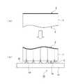
たとえば、フォトマスクブランクに対し、描画装置を用いてパターンを描画する際には、描画装置のステージ上に、膜面を上向きにした状態でフォトマスクブランクが載置される。その際、ステージのフラットネス(平坦度)が十分でない場合、あるいは、ステージに対面するフォトマスクブランクの裏面のフラットネスが十分でない場合には、その凹凸がフォトマスクブランクの表面形状に影響し、この状態で描画が行われる。具体的には、たとえば図8(a)に示すように、フォトマスク用の基板(以下、単に「基板」ともいう。)51の表面52が膜面となっていて、その反対側の裏面53のフラットネスが十分でない場合、図8(b)に示すように、膜面である表面2を上向きにして基板51をステージ61上に載置したときに、基板51の裏面53が重力によってステージ61の平面62に倣い、基板51の表面52の形状が裏面53の凹凸の影響を受けて変化してしまう。また仮に、ステージ61の平面62が凹凸のない理想的な平面であり、裏面53のフラットネスが非常に高い高精度な基板51を使用していたとしても、そのステージ61の平面62と基板51の裏面53との間に異物63の挟み込みが生じれば、その影響で基板51の膜面形状(表面形状)に変化が生じる。 For example, when a pattern is drawn on a photomask blank using a drawing apparatus, the photomask blank is placed on the stage of the drawing apparatus with the film surface facing upward. At that time, when the flatness (flatness) of the stage is not sufficient, or when the flatness of the back surface of the photomask blank facing the stage is not sufficient, the unevenness affects the surface shape of the photomask blank, Drawing is performed in this state. Specifically, for example, as shown in FIG. 8A, a
その一方、パターニング等によって転写用パターンを形成し、完成品となったフォトマスクを露光装置にセットする際には、描画時に上向きであった膜面が下向きになるため、上記の膜面形状の変化が消失した状態になる。したがって、描画時と露光時では膜面形状が異なり、その影響で露光時の座標精度が劣化することとなる。 On the other hand, when a transfer pattern is formed by patterning or the like, and a completed photomask is set in an exposure apparatus, the film surface that was upward at the time of drawing is directed downward. Changes are lost. Therefore, the film surface shape is different at the time of drawing and at the time of exposure, and the coordinate accuracy at the time of exposure deteriorates due to the influence.
特許文献1の記載の技術では、描画時と露光時の膜面形状の差異を、描画データの補正によって解決するものである。すなわち、描画時と露光時との膜面形状の差異に由来する座標ずれを相殺するべく、描画データ又は描画時に適用する座標に補正を施しておくことにより、露光時の座標精度の劣化を防止している。しかしながら、描画装置内で基板の膜面が受ける変形要因自体を抑制し、理想平面に近い状態にすることで、上記の描画データの補正の必要性を小さくし、あるいは、不要とすることは、フォトマスクの座標精度を高く維持するための、より根本的な手法とも考えられる。 In the technique described in Patent Document 1, the difference in film surface shape between drawing and exposure is solved by correcting drawing data. That is, by correcting the drawing data or the coordinates applied at the time of drawing in order to offset the coordinate deviation resulting from the difference in film surface shape between the drawing time and the exposure time, deterioration of the coordinate accuracy at the time of exposure is prevented. doing. However, by suppressing the deformation factor itself that the film surface of the substrate receives in the drawing apparatus and making it close to the ideal plane, the necessity for correcting the drawing data described above is reduced or unnecessary. It can also be considered as a more fundamental technique for maintaining high photomask coordinate accuracy.
特許文献2に記載の基板保持装置は、ステージの上面に、凸部と、基板の下面に気体を吹き付けるための吐出孔とを備え、この凸部が、基板を載置する載置面と基板を吸着して保持する保持手段を有し、基板に下方から気体を吹き付けることで、自重による基板の撓みを低減するものである。ただし、この基板保持装置では、凸部と基板との間の異物の挟み込みや、基板の吸着に起因して、基板の変形が生じるリスクがある。 The substrate holding apparatus described in
そこで、本発明は、上記課題を解決するべく、被転写体上に形成されるパターンの座標精度を高めることのできる、フォトマスク基板に適した基板保持装置、描画装置、フォトマスク検査装置、およびフォトマスクの製造方法を提供しようとするものである。 In view of the above, the present invention provides a substrate holding device, a drawing device, a photomask inspection device, and a photomask substrate that can improve the coordinate accuracy of a pattern formed on a transfer object, in order to solve the above problems. An object of the present invention is to provide a method for manufacturing a photomask.
(第1の態様)
本発明の第1の態様は、
表示装置製造用のフォトマスク基板を水平に保持する基板保持装置であって、
低膨張材料からなるステージと、
前記ステージ上に設けられた複数の支持具と、を備え、
前記支持具は、先端に、凸曲面をもつ接触部を備え、前記接触部が、前記フォトマスク基板の下面側主表面に、実質的に点接触又は線接触することで、前記フォトマスク基板を水平に保持することを特徴とする、
基板保持装置である。
(第2の態様)
本発明の第2の態様は、
前記支持具は、先端に、球面をもつ接触部を備え、前記接触部が、前記フォトマスク基板の下面側主表面に、実質的に点接触することを特徴とする、
上記第1の態様に記載の基板保持装置である。
(第3の態様)
本発明の第3の態様は、
前記ステージを、基台上に非接触状態で水平に保持するための、浮上機構を備えることを特徴とする、
上記第1又は第2の態様に記載の基板保持装置である。
(第4の態様)
本発明の第4の態様は、
前記複数の支持具は、互いの距離が150mm以下となるように、前記ステージ上に配列されていることを特徴とする、
上記第1〜第3の態様のいずれかに記載の基板保持装置である。
(第5の態様)
本発明の第5の態様は、
前記複数の支持具は、各々が高さ調整機構をもつことを特徴とする、
上記第1〜第4の態様のいずれかに記載の基板保持装置である。
(第6の態様)
本発明の第6の態様は、
前記高さ調整機構は、気体の圧力を利用するものである、
上記第5の態様に記載の基板保持装置である。
(第7の態様)
本発明の第7の態様は、
前記高さ調整機構は、磁気による反発力を利用するものである、
上記第5の態様に記載の基板保持装置である。
(第8の態様)
本発明の第8の態様は、
前記高さ調整機構は、高さ調整量に応じて、前記接触部の高さ位置を調整する駆動装置を備えることを特徴とする、
上記第5の態様に記載の基板保持装置である。
(第9の態様)
本発明の第9の態様は、
上記第1〜第8の態様のいずれかに記載の基板保持装置を含む、
描画装置である。
(第10の態様)
本発明の第10の態様は、
上記第1〜第8の態様のいずれかに記載の基板保持装置を含む、
フォトマスク検査装置である。
(第11の態様)
本発明の第11の態様は、
透明材料からなるフォトマスク基板の主表面に、光学膜とフォトレジスト膜を形成したフォトマスクブランクを用意する工程と、
前記フォトマスクブランクを、上記第1〜第7の態様のいずれかに記載の基板保持装置により保持する工程と、
前記保持したフォトマスクブランクに対して、パターンデータに基づく描画を行い、前記光学膜をパターニングする工程と、
を含む、
フォトマスクの製造方法である。
(第12の態様)
本発明の第12の態様は、
透明材料からなるフォトマスク基板の主表面に、光学膜とフォトレジスト膜を形成したフォトマスクブランクを用意する工程と、
前記フォトマスクブランクに対して、パターンデータに基づく描画を行い、前記光学膜をパターニングして、転写用パターンをもつフォトマスクとする工程と、
前記転写用パターンを検査する工程と、
を含む、フォトマスクの製造方法であって、
前記検査する工程においては、上記第1〜第7の態様のいずれかに記載の基板保持装置により前記フォトマスクを保持して、座標精度を検査することを含む、
フォトマスクの製造方法である。
(第13の態様)
本発明の第13の態様は、
透明材料からなるフォトマスク基板の主表面に、光学膜とフォトレジスト膜を形成したフォトマスクブランクを用意する工程と、
前記フォトマスクブランクを、前記主表面を上側にして、基板保持装置により保持する保持工程と、
前記保持したフォトマスクブランクに対して、パターンデータに基づく描画を行う描画工程と、を有し、
前記基板保持装置は、前記フォトマスク基板を載置するステージと、前記ステージ上に設けられ、各々高さ調整機構を備えた複数の支持具を有し、
前記保持工程においては、前記主表面の高さ分布を測定して、高さ分布データを得るとともに、前記高さ分布データに基づいて、前記高さ調整機構を駆動させ、前記フォトマスクブランクの主表面形状を調整することを含む、
フォトマスクの製造方法である。(First aspect)
The first aspect of the present invention is:
A substrate holding device for horizontally holding a photomask substrate for manufacturing a display device,
A stage made of a low expansion material;
A plurality of supports provided on the stage,
The support includes a contact portion having a convex curved surface at a tip, and the contact portion substantially makes point contact or line contact with a lower surface side main surface of the photomask substrate, whereby the photomask substrate is formed. Characterized by being held horizontally,
A substrate holding device.
(Second aspect)
The second aspect of the present invention is:
The support includes a contact portion having a spherical surface at a tip, and the contact portion substantially makes point contact with a lower surface side main surface of the photomask substrate.
A substrate holding apparatus according to the first aspect.
(Third aspect)
The third aspect of the present invention is:
It is characterized by comprising a levitation mechanism for holding the stage horizontally on the base in a non-contact state,
A substrate holding apparatus according to the first or second aspect.
(Fourth aspect)
The fourth aspect of the present invention is:
The plurality of supports are arranged on the stage so that the distance between them is 150 mm or less,
The substrate holding device according to any one of the first to third aspects.
(5th aspect)
According to a fifth aspect of the present invention,
Each of the plurality of supports has a height adjustment mechanism,
The substrate holding apparatus according to any one of the first to fourth aspects.
(Sixth aspect)
The sixth aspect of the present invention is:
The height adjusting mechanism uses gas pressure.
The substrate holding apparatus according to the fifth aspect.
(Seventh aspect)
The seventh aspect of the present invention is
The height adjusting mechanism uses a magnetic repulsive force.
The substrate holding apparatus according to the fifth aspect.
(Eighth aspect)
The eighth aspect of the present invention is
The height adjustment mechanism includes a driving device that adjusts a height position of the contact portion according to a height adjustment amount.
The substrate holding apparatus according to the fifth aspect.
(Ninth aspect)
The ninth aspect of the present invention provides
Including the substrate holding apparatus according to any one of the first to eighth aspects,
A drawing device.
(Tenth aspect)
The tenth aspect of the present invention provides
Including the substrate holding apparatus according to any one of the first to eighth aspects,
This is a photomask inspection apparatus.
(Eleventh aspect)
The eleventh aspect of the present invention is
A step of preparing a photomask blank in which an optical film and a photoresist film are formed on a main surface of a photomask substrate made of a transparent material;
A step of holding the photomask blank by the substrate holding device according to any one of the first to seventh aspects;
For the held photomask blank, drawing based on pattern data and patterning the optical film;
including,
It is a manufacturing method of a photomask.
(Twelfth aspect)
The twelfth aspect of the present invention provides
A step of preparing a photomask blank in which an optical film and a photoresist film are formed on a main surface of a photomask substrate made of a transparent material;
For the photomask blank, performing drawing based on pattern data, patterning the optical film, and forming a photomask having a transfer pattern;
Inspecting the transfer pattern;
A method of manufacturing a photomask, comprising:
The step of inspecting includes holding the photomask by the substrate holding device according to any one of the first to seventh aspects, and inspecting the coordinate accuracy.
It is a manufacturing method of a photomask.
(13th aspect)
The thirteenth aspect of the present invention provides
A step of preparing a photomask blank in which an optical film and a photoresist film are formed on a main surface of a photomask substrate made of a transparent material;
A holding step of holding the photomask blank by a substrate holding device with the main surface facing upward;
A drawing process for drawing based on pattern data for the held photomask blank,
The substrate holding device has a stage on which the photomask substrate is placed, and a plurality of supports provided on the stage, each having a height adjusting mechanism,
In the holding step, the height distribution of the main surface is measured to obtain height distribution data, and the height adjustment mechanism is driven based on the height distribution data to Including adjusting the surface shape,
It is a manufacturing method of a photomask.
本発明によれば、フォトマスク基板を保持するステージ上の異物の挟み込みによる、フォトマスク膜面形状の変化を抑止し、フォトマスクのもつ転写用パターンを、優れた座標精度で被転写体上に転写することが可能となる。 According to the present invention, it is possible to suppress a change in the shape of the photomask film surface due to the inclusion of foreign matter on the stage holding the photomask substrate, and to transfer the transfer pattern of the photomask onto the transfer target with excellent coordinate accuracy. It becomes possible to transfer.
一般に、フォトマスクブランクへの描画などの目的で、基板を水平に保持する基板保持装置が用いられている。この基板保持装置は、基板を載置するためのステージとして、平坦かつ平滑に加工されたステージを備えている。そして、実際に基板を保持する場合は、このステージ上に、膜面となる表面を上向きにして基板を載置する。 In general, a substrate holding apparatus that horizontally holds a substrate is used for the purpose of drawing on a photomask blank. This substrate holding device includes a stage that is processed flat and smooth as a stage for placing a substrate. When the substrate is actually held, the substrate is placed on this stage with the film surface facing upward.
本明細書において、膜面とは、表裏の関係で基板が有する2つの主表面のうち、次のような面をいう。すなわち、パターン形成前の透明材料からなる基板であれば、パターンを形成する予定の面をいい、所定の光学膜やレジスト膜が形成されたフォトマスクブランクであれば、これらの膜が形成された面をいい、転写用パターンが形成されたフォトマスク、又はその半製品であるフォトマスク中間体であれば、転写用パターンが形成された面をいう。また、膜面に該当する主表面を表面とし、膜面とは反対側の主表面を裏面とする。 In this specification, a film surface means the following surfaces among two main surfaces which a board | substrate has by the relationship of front and back. That is, if it is a substrate made of a transparent material before pattern formation, it refers to the surface on which a pattern is to be formed. If it is a photomask blank on which a predetermined optical film or resist film is formed, these films are formed. In the case of a photomask on which a transfer pattern is formed, or a photomask intermediate that is a semi-finished product thereof, the surface on which the transfer pattern is formed. The main surface corresponding to the film surface is the front surface, and the main surface opposite to the film surface is the back surface.
ここで、基板保持装置のステージの表面が清浄かつ理想平面であり、そこに載置される基板の表面(膜面)および裏面も理想平面であれば、座標精度が劣化する問題は生じない。しかしながら、仮に、フォトマスク用の基板を用意する段階で、精密な研磨を両主表面に施すといっても、たとえば、裏面の平坦度が十分でない場合や、ステージと基板の間に異物の挟み込みがある場合は、これらの影響を受けて、ステージに載置した基板の膜面形状が変化してしまう(図8を参照)。 Here, if the surface of the stage of the substrate holding device is clean and ideal plane, and the front surface (film surface) and back surface of the substrate placed thereon are also ideal planes, there is no problem that the coordinate accuracy deteriorates. However, even if it is said that precise polishing is applied to both main surfaces at the stage of preparing the substrate for the photomask, for example, when the flatness of the back surface is not sufficient or foreign matter is sandwiched between the stage and the substrate If there is, the film surface shape of the substrate placed on the stage changes under these influences (see FIG. 8).
したがって、上述のように膜面形状が変化した状態で基板の膜面側に所定のパターンデータによる描画を施すと、これによって形成された転写用パターンを露光装置によって被転写体に転写するとき、すなわち、裏面側の凹凸や異物による上記膜面形状の変化が消失した状態で転写するときには、座標精度が失われ、歪が生じてしまう。もちろん、座標精度の劣化は、高精度に研磨された基板を用いることにより、ある程度軽減することは可能である。たとえば、基板の膜面側のみならず、裏面側の平坦度も高い規格で加工された高精度な基板を用いれば、描画時の膜面形状の変化を抑えることができる。ただし、基板保持装置のステージ上に偶発的に発生する異物の存在を完全に排除することはできない。 Therefore, when drawing with predetermined pattern data on the film surface side of the substrate with the film surface shape changed as described above, when the transfer pattern formed thereby is transferred to the transfer object by the exposure device, That is, when the transfer is performed in a state in which the change in the film surface shape due to the unevenness on the back surface side or the foreign matter has disappeared, the coordinate accuracy is lost and distortion occurs. Of course, the deterioration of the coordinate accuracy can be reduced to some extent by using a highly polished substrate. For example, if a highly accurate substrate processed according to a standard with high flatness not only on the film surface side of the substrate but also on the back surface side, changes in the film surface shape during drawing can be suppressed. However, it is impossible to completely eliminate the presence of foreign matters that occur on the stage of the substrate holding apparatus.
そこで、本実施形態では、このような異物の存在による座標精度の劣化を更に抑止するため、ステージへの基板裏面の接触を、実質的に点接触又は線接触とし、異物を挟み込む確率を低減するように構成した。 Therefore, in this embodiment, in order to further suppress deterioration of coordinate accuracy due to the presence of such foreign matter, the contact of the back surface of the substrate with the stage is substantially point contact or line contact, and the probability of pinching foreign matter is reduced. It was configured as follows.
具体的には、本実施形態に係る基板保持装置は、表示装置製造用のフォトマスク基板を水平に保持する基板保持装置であって、低膨張材料からなるステージと、このステージ上に設けられた複数の支持具と、を備える。また、各々の支持具は、先端に、凸曲面をもつ接触部を備え、この接触部が、フォトマスク基板の下面側主表面に、実質的に点接触又は線接触することで、フォトマスク基板を水平に保持する構成となっている。 Specifically, the substrate holding device according to the present embodiment is a substrate holding device that horizontally holds a photomask substrate for manufacturing a display device, and is provided on a stage made of a low expansion material and on this stage. A plurality of supports. In addition, each support has a contact portion having a convex curved surface at the tip, and this contact portion substantially makes point contact or line contact with the lower surface side main surface of the photomask substrate, so that the photomask substrate Is held horizontally.
本明細書において、保持の対象となるフォトマスク基板(以下、「マスク基板」、又は単に「基板」ともいう。)は、透明材料からなる基板でもよく、この基板のいずれかの主表面に、得ようとする転写用パターンに適した所望の光学膜(露光光を遮光する遮光膜、露光光を一部透過する半透光膜、露光光を一部透過するとともに、光の位相をシフトする位相シフト膜、露光光を含む光の反射を防止する反射防止膜などを含む)又は機能膜(エッチングストッパ膜、導電性調整膜など)が成膜されたフォトマスクブランクでもよく、更にフォトレジストなどのレジスト膜が形成されたレジスト付フォトマスクブランクでもよく、転写用パターンが部分的に又は完全に形成された、フォトマスク中間体やフォトマスクでもよい。 In this specification, a photomask substrate to be held (hereinafter, also referred to as “mask substrate” or simply “substrate”) may be a substrate made of a transparent material. Desired optical film suitable for the transfer pattern to be obtained (a light-shielding film that blocks exposure light, a semi-transparent film that partially transmits exposure light, a part that transmits exposure light, and shifts the phase of light) A photomask blank on which a phase shift film, an antireflection film for preventing reflection of light including exposure light, etc.) or a functional film (such as an etching stopper film or a conductive adjustment film) may be formed, and a photoresist, etc. It may be a photomask blank with a resist on which a resist film is formed, or a photomask intermediate or a photomask in which a transfer pattern is partially or completely formed.
<第1実施形態>
図1は本発明の第1実施形態に係る基板保持装置の構成を説明するための図であって、(a)は保持前のフォトマスク基板の状態を示す側面図、(b)はフォトマスク基板を基板保持装置により保持した状態を示す側面図である。<First Embodiment>
FIG. 1 is a view for explaining the configuration of a substrate holding apparatus according to a first embodiment of the present invention, wherein (a) is a side view showing a state of a photomask substrate before holding, and (b) is a photomask. It is a side view which shows the state which hold | maintained the board | substrate with the board | substrate holding | maintenance apparatus.
(フォトマスク基板)
図1(a)に示すフォトマスク基板1は、一方の主表面である表面2を膜面とし、そこに遮光膜等が成膜されたフォトマスクブランクである。フォトマスク基板1は、平面視四角形(正方形又は長方形)に形成されている。また、ここで例示するフォトマスク基板1は、自重による撓みを受けない状態で平坦度測定を行ったときに、図1(a)に示す形状をもつ。図示したフォトマスク基板1は、表面2の平坦度が高くなるように高精度に研磨された基板であるが、裏面3には若干の凹凸がある。(Photomask substrate)
A photomask substrate 1 shown in FIG. 1A is a photomask blank in which a
自重による撓みの影響を受けないで平坦度測定を行う方法としては、たとえば、基板の主表面(表面および裏面)を鉛直に保持し、その状態で基板の表面および裏面の平坦度をそれぞれ平坦度測定装置などにより測定する方法がある。この方法によって得られた測定結果を、表面平坦度データ、裏面平坦度データとし、マップ化するなどすれば、基板の表面および裏面の形状を把握することができる。 As a method for measuring the flatness without being affected by the deflection due to its own weight, for example, the main surface (front surface and back surface) of the substrate is held vertically, and the flatness of the front surface and back surface of the substrate is maintained in this state. There is a method of measuring with a measuring device. If the measurement results obtained by this method are used as the surface flatness data and the back surface flatness data and mapped, the shapes of the front and back surfaces of the substrate can be grasped.
(基板保持装置)
図1(b)に示す基板保持装置10は、フォトマスク基板を水平に保持するものである。基板保持装置10は、ステージ11を備えている。ステージ11は、低膨張材料によって構成されている。低膨張材料は、温度変化による体積変化が小さい材料である。たとえば、セラミックスなどであって、常温付近での熱膨張係数が極めて低い材料を好適に使用することができる。好ましくは、熱膨張係数が摂氏0〜50度で、0.1×10⁻⁶/K以下の材料を、ステージ11の構成材料に用いることができる。なお、本明細書において、数値範囲を規定する「○○〜△△」の表記は、「○○以上△△以下」を意味する。(Substrate holding device)
A
ステージ11は、フォトマスク基板1と同様に平面視四角形(正方形又は長方形)に形成されている。ステージ11上には複数の支持具12が設けられている。各々の支持具12は、柱状のピン構造をなす支持具(以下、「支持ピン」ともいう。)であって、ステージ11の表面(上面)から上側に突出する状態で設けられている。各支持ピンはステージ11上に固定され、支持ピンの高さは固定されている(高さ固定タイプ)。ここでは、一定の高さに設定されている。 The
各々の支持具(支持ピン)12の先端には、上側が凸曲面となる接触部14が形成されている。接触部14は、基板保持装置10によってフォトマスク基板1を保持する際に、フォトマスク基板1の裏面(下面)3に接触する部分となる。接触部14は、硬質の材料によって構成されている。この接触部14は、たとえば、ボール形状(球面形状)とした接触部14を支持ピンの先端に取り付けることにより、フォトマスク基板1の裏面3に対して実質的に点接触する部分となる。 At the tip of each support tool (support pin) 12, a
実際に、基板の裏面3を下向きにしてフォトマスク基板1をステージ11上に載置した状態では、基板の下側主表面となる裏面3が、複数の支持具12の先端に実質的に点接触で支承され、その状態でフォトマスク基板1が水平に保持される。このとき、複数の支持具(支持ピン)12が接触部14を介して、フォトマスク基板1の裏面3側から基板の重量を支えることで、フォトマスク基板1が水平に保持される。また、ステージ11上に少なくとも4つの支持具12を配置した場合、フォトマスク基板1は、裏面3側を少なくとも4点の点接触で支持されるとともに、その重量を支承されることになる。尚、凸曲面をもつ接触部14と基板裏面3との接触は原理的に点接触であるが、接触部14が基板重量を受けてわずかに変形する場合においても、該接触は実質的に点接触であり、本発明の作用効果が得られることから、本発明はそのような状態を包含するものとする。この点は、後述する線接触においても同様である。 Actually, in a state in which the photomask substrate 1 is placed on the
接触部14の素材としては、たとえばルビーやサファイアなどの硬質の材料を好適に使用することができる。ただし、これ以外にも、比較的硬度の高い金属を用いて接触部14を構成してもよい。たとえば、ビッカース硬度が800kgw/mm2以上の素材が好ましく用いられる。接触部14を硬度が低い材料で構成すると、磨耗によって点接触が維持できなくなり、たびたび交換が必要になる。これに対して、接触部14を硬度の高い材料で構成すれば、接触部14の摩耗が抑えられるため、長期にわたって点接触の状態を維持することができる。As a material of the
また、本実施形態に係る基板保持装置10は、図2(a)に示すように、ステージ11の下に基台15を備えている。基台15は、ステージ11と同様に平面視四角形(正方形又は長方形)に形成されている。ステージ11は、基台15上に水平に載置される構成であるが、より好ましくは、基台15上に非接触状態で水平に保持する機能を有する構成とするのがよい。具体的には、たとえば、気体の圧力などによりステージ11を浮上させる浮上機構を備え、この浮上機構によりステージ11を基台15上に非接触状態で水平に保持する構成を備えるものとすることができる。その場合、ステージ11は、基台15上で水平な姿勢を維持したまま、気体の圧力(たとえば、空気圧)により浮上する構成とすることが好ましい。これにより、たとえば、描画装置において、フォトマスク基板1を保持するステージ11を水平に移動させる必要がある場合には、図中の矢印で示すようにステージ11を基台15から所定高さに浮上させ、その状態でステージ11を水平に移動させることができる。 In addition, the
支持具12は、図2(b)に示すように、先端に、凸曲面(本態様では球面)をもつ接触部14を備えている。支持具12は、ステージ11上に、一定のピッチで規則的に配列されていることが好ましい。その場合、複数の支持具12は、互いの間隔が、150mm以下、より好ましくは、60〜150mm、さらに好ましくは、60〜130mmとなるように、ステージ11上に配列されていることが望ましい。図2(a)においては、一例として、複数の支持具12をステージ11上に格子状に配列している。支持具12を支持ピンで構成する場合は、隣り合う支持ピンの間隔(中心間距離)が、上述のように最大でも150mm以下となるように、支持ピンを規則的に配列することが好ましい。 As shown in FIG. 2B, the
また、支持具12を支持ピンで構成する場合、支持ピンはステージ11上に少なくとも4本設けることが好ましい。その場合、基板保持装置10に保持されるフォトマスク基板1に対しては、ステージ11に対向する裏面3の少なくとも4点に、それぞれに対応する支持具12の接触部14が接触する。そして、この4点の接触により、フォトマスク基板1の重量が各々の支持具12によって支承される。 Further, when the
ここで、フォトマスク基板1の大きさや重量に対して、ステージ11上に配置する支持ピンの個数が少なすぎると、支持ピンの間で基板に撓みが生じ、座標精度に悪影響をおよぼすおそれがある。また、支持ピンの配置個数が多すぎると、それだけ支持ピンと基板との接触点数が増えるため、支持ピンと基板との間に異物の介在する確率が高くなってしまう。特に、表示装置製造用のフォトマスク基板は、たとえば、主表面の一辺が300mm以上の正方形又は長方形で面積が大きく、重量もあるため、3点以下の接触で支持することが困難である。このため、表示装置製造用のフォトマスク基板を、支持ピンによる点接触で支持する場合は、好ましくは、9〜350点、より好ましくは、36〜300点の接触点で支持することが好ましい。上記のとおり、各接触点の高さは、等しくなるように設定することができる。又は、裏面平坦度データを用い、裏面の高さ分布を相殺するように、各接触点の高さを調整して設定してもよい。 Here, if the number of support pins arranged on the
本第1実施形態においては、フォトマスク基板1を基板保持装置10によって水平に保持する場合に、ステージ11上に設けられた複数の支持具12がそれぞれ接触部14を介してフォトマスク基板1の裏面3に点接触する構成になっている。このような構成を適用すれば、フォトマスク基板1の裏面3側がステージ11上に面接触で載置されることがなく、フォトマスク基板1が複数の支持具12によりステージ11の上面から浮いた状態に保持されるため、ステージ11上面とフォトマスク基板1裏面との間に異物16(図1)を挟み込むことがない。また、フォトマスク基板1を各々の支持具12が点接触で支持するため、フォトマスク基板1裏面と支持具12先端との間に異物を挟み込むことは生じにくい。したがって、この状態でフォトマスク基板1の膜面側への処理(たとえば、描画処理)を行えば、異物16の挟み込みに起因する膜面形状の変化を抑止することができる。よって、膜面形状の変化による座標精度の劣化を抑えることができる。その結果、フォトマスク基板1に形成される転写用パターンを、優れた座標精度で被転写体に転写することが可能となる。 In the first embodiment, when the photomask substrate 1 is held horizontally by the
このように、本第1実施形態では、異物16の挟み込みに起因するフォトマスク基板1の膜面形状の変化を抑止することにより、描画時と露光時との膜面形状の相違による座標精度の劣化を抑えることができる。これにより、異物16の挟み込みによってフォトマスク基板1が変形するというリスクを防ぎ、被転写体上に形成されるパターンの座標精度を高めるという所期の目的を達成することができる。 As described above, in the first embodiment, by suppressing the change in the film surface shape of the photomask substrate 1 caused by the inclusion of the
ただし、フォトマスク基板1の裏面3の平坦度不足に由来する凹凸については、その影響を抑止するための更なる工夫を行うことができる。すなわち、裏面3のフラットネスが不十分のために、裏面3に凹凸がある場合には、基板保持装置10のステージ11上に水平に載置されたフォトマスク基板1の膜面側に、上記の凹凸が反映される。したがって、その状態で行われる基板膜面への処理(たとえば、描画処理)後の座標精度に悪影響をおよぼすおそれがある。そこで、本発明者は、上記第1実施形態よりも更に高い座標精度を得ることができる基板保持装置を考え出した。以下に、具体的な態様を第2実施形態および第3実施形態として説明する。 However, with regard to the unevenness resulting from the lack of flatness of the
<第2実施形態>
図3は本発明の第2実施形態に係る基板保持装置の構成を説明するための図であって、(a)は保持前のフォトマスク基板の状態を示す側面図、(b)はフォトマスク基板を基板保持装置により保持した状態を示す側面図である。Second Embodiment
3A and 3B are diagrams for explaining the configuration of the substrate holding apparatus according to the second embodiment of the present invention, in which FIG. 3A is a side view showing a state of the photomask substrate before holding, and FIG. 3B is a photomask. It is a side view which shows the state which hold | maintained the board | substrate with the board | substrate holding | maintenance apparatus.
(フォトマスク基板)
図3(a)に示すフォトマスク基板1は、上記第1実施形態と同様に、一方の主表面である表面2を膜面とし、そこに遮光膜等が成膜されたフォトマスクブランクである。ただし、上記第1実施形態で用いたフォトマスク基板1と比べると、平坦度の規格が緩くなっていてもよい。すなわち、ここで例示するフォトマスク基板1は、自重による撓みを受けない状態で平坦度測定を行ったときに、表面2の平坦度は第1実施形態と同様に高いものの、裏面3の凹凸は第1実施形態よりも大きく、基板の厚さが不均一になっている。(Photomask substrate)
The photomask substrate 1 shown in FIG. 3A is a photomask blank having a
(基板保持装置)
図3(b)に示す基板保持装置10では、低膨張材料からなるステージ11上に複数の支持具12が設けられている。この点は上記第1実施形態と同様である。ただし、上記第1実施形態では、各々の支持具12を構成する支持ピンの高さが固定されていたのに対して、本第2実施形態では、各々の支持具12に高さ調整機構20が備えられている。高さ調整機構20は、気体の圧力(たとえば、空気圧など)を利用して、支持具12における接触部14の高さ位置を調整するものである。高さ調整機構20は、接触部14の高さ位置を調整する駆動装置として、たとえば図4に示すように、エアダンパ21と、このエアダンパ21への給気および排気によって上下方向に移動可能なロッド22と、を備えている。ロッド22の先端(上端)には、突子23を介してボール形状の接触部14が取り付けられている。ボール形状の接触部14は、受ける負荷に応じて上下可動に保持されている。(Substrate holding device)
In the
なお、ここでは一例として、高さ調整機構20は、気体の圧力を利用するものとしたが、これに限らず、たとえば、磁気による反発力を利用するものであってもよい。 Here, as an example, the
上記構成からなる高さ調整機構20においては、エアダンパ21に対して圧縮空気を供給したり、供給した圧縮空気を排気したりすることにより、ロッド22を上下方向に移動(昇降)させることができる。また、接触部14に負荷が加わる状況において、エアダンパ21に供給する圧縮空気の圧力を可変制御することにより、接触部14の高さを調整(変更)することができる。また、ステージ11上にフォトマスク基板1を載せない状態で、高さ調整機構20のエアダンパ21に圧縮空気を供給すると、ロッド22の上昇によって接触部14が押し上げられる。このとき、支持具12の接触部14には、圧縮空気の圧力に応じた押し上げ力が働く。このため、ステージ11上に設けられた全ての支持具12の高さ調整機構20に対して、それぞれ同じ圧力の圧縮空気を供給することにより、各々の支持具12の接触部14を互いに同じ押し上げ力によって上昇させることができる。 In the
上記構成からなる基板保持装置10を用いてフォトマスク基板1を保持する場合は、その表面2を上向き、裏面3を下向きにして、ステージ11上にフォトマスク基板1を載置する。そうすると、上記第1実施形態と同様に、ステージ11上に設けられた各々の支持具12上に、フォトマスク基板1が、接触部14を介して点接触で支承される。また、各々の支持具12の高さ調整機構20に圧縮空気を供給して接触部14を上昇させ、その状態でフォトマスク基板1を載せると、各々の支持具12に対して、フォトマスク基板1の自重による重力が下向きに加わる。このとき、各々の支持具12では、ロッド22を介して接触部14に作用する押し上げ力と、フォトマスク基板1の自重によって接触部14に作用する重力とが、ちょうど釣り合う高さ位置で、接触部14が静止する。したがって、ステージ11上にフォトマスク基板1を載置する場合は、フォトマスク基板1の自重による重力と、高さ調整機構20による押し上げ力とが、互いに釣り合う(ほぼ等しくなる)ように、各々の高さ調整機構20に供給する圧縮空気の圧力を設定すればよい。 When holding the photomask substrate 1 using the
本第2実施形態では、各々の高さ調整機構20に均等な圧力で圧縮空気を供給する構成を採用している。これにより、フォトマスク基板1の裏面3のフラットネスが不十分である故に裏面3に凹凸がある場合でも、裏面3の凹凸形状をそのまま維持した状態で、各々の支持具12の接触部14によりフォトマスク基板1を水平に支持することができる。その理由は、次のとおりである。フォトマスク基板1の裏面3には、凹凸によって相対的に厚みが大きい部分(面積あたりの重量が大きい部分)と相対的に厚みが小さい部分(面積あたりの重量が小さい部分)が存在する。これに対して、各々の高さ調整機構20に均等な圧力で圧縮空気が供給されている場合、上記相対的に厚みが大きい部分に点接触する接触部14は、より大きな重力を受けるため、相対的に低い位置で静止する。一方、上記相対的に厚みが小さい部分に点接触する接触部14は、より小さな重力を受けるため、相対的に高い位置で静止する。つまり、フォトマスク基板1の裏面3の凹凸によって、各々の接触部14が静止する高さ位置が異なる。したがって、用いる基板の裏面形状に応じて(受動的に)、接触部14の高さ調整が可能となる。この点は、ステージ11上にフォトマスク基板1を載せた後で各々の高さ調整機構20に均等な圧力で圧縮空気を供給した場合でも同様である。 In the second embodiment, a configuration is adopted in which compressed air is supplied to each
したがって、本第2実施形態においては、フォトマスク基板1の裏面3に凹凸があっても、この凹凸を各々の接触部14の高さ位置の違いによって吸収することができる。よって、フォトマスク基板1の裏面3の凹凸形状を表面(膜面)2側に反映させることなく、フォトマスク基板1を水平に保持することができる。また、ステージ11上に存在する異物16や、裏面3の平坦度不足に由来する凹凸があったとしても、この影響を低減し、膜面の水平(平坦性)を高いレベルで維持することができる。そして、この基板保持装置10に載置されたフォトマスク基板1への処理(たとえば、描画処理)に際して、座標精度の劣化をより一層抑制することが可能となる。 Therefore, in the second embodiment, even if the
<第3実施形態>
図5は本発明の第3実施形態に係る基板保持装置の構成を説明するための図であって、(a)は保持前のフォトマスク基板の状態を示す側面図、(b)は高さ調整機構を駆動させずにフォトマスク基板を基板保持装置により保持した状態を示す側面図、(c)は高さ調整機構を駆動させてフォトマスク基板を基板保持装置により保持した状態を示す側面図である。<Third Embodiment>
FIGS. 5A and 5B are diagrams for explaining the configuration of the substrate holding apparatus according to the third embodiment of the present invention. FIG. 5A is a side view showing the state of the photomask substrate before holding, and FIG. The side view which shows the state which hold | maintained the photomask substrate by the substrate holding apparatus, without driving an adjustment mechanism, (c) is the side view which shows the state which driven the height adjustment mechanism, and was hold | maintained by the substrate holding apparatus. It is.
(フォトマスク基板)
図5(a)に示すフォトマスク基板1は、上記第2実施形態と同様に、一方の主表面である表面2を膜面とし、そこに遮光膜等が成膜されたフォトマスクブランクである。このフォトマスク基板1は、自重による撓みを受けない状態で平坦度測定を行ったときに、表面2の平坦度は第1実施形態と同様に高いものの、裏面3の凹凸は第1実施形態よりも大きく、基板の厚さが不均一になっている。(Photomask substrate)
The photomask substrate 1 shown in FIG. 5A is a photomask blank in which the
(基板保持装置)
図5(b),(c)に示す基板保持装置10では、低膨張材料からなるステージ11上に複数の支持具12が設けられ、各々の支持具(支持ピン)12に高さ調整機構20が備えられている。この点は上記第2実施形態と同様である。ただし、本第3実施形態においては、複数の支持具(支持ピン)12の各々が独立に高さ調整可能な高さ調整機構20を備える点で、上記第2実施形態とは異なる。すなわち、複数の支持具12に対応する複数の高さ調整機構20は、それぞれに指定された高さ調整量に応じて(能動的に)、接触部14の位置を上昇させる駆動装置を備えている。具体的には、たとえば、高さ調整機構20の駆動装置を上記図4に示したエアダンパ21とロッド22を用いて構成し、これによって高さ調整機構20が気体の圧力(ここでは空気圧とする)を利用して接触部14の高さを調整するものであれば、エアダンパ21に供給する圧縮空気の圧力を、各々の高さ調整機構20ごとに個別に制御可能な構成とする。これにより、フォトマスク基板1を水平に保持する際には、複数の支持具12における接触部14の高さをそれぞれ独立に調整することが可能となる。また、各々の支持具12ごとに、それぞれ指定された高さ調整量に応じて、接触部14の位置を所望の押し上げ力をもって上昇させることが可能となる。(Substrate holding device)
In the
ここで、図5(b)に示すように、高さ調整機構20を駆動させずにフォトマスク基板1を基板保持装置10により保持したときに、ある部分では、支持具12の接触部14とフォトマスク基板1の裏面3との間に、異物16が挟み込まれた状況を考える。この状況では、図5(a)に示すフォトマスク基板1の裏面3の凹凸と、同図(b)に示す異物16の挟み込みとに起因して、裏面3側の凹凸や異物16の挟み込みがフォトマスク基板1の表面2側に反映され、膜面の平坦度が不十分となるリスクがある。 Here, as shown in FIG. 5B, when the photomask substrate 1 is held by the
そこで本第3実施形態では、各々の高さ調整機構20を駆動するのに先立ち、図5(b)に示す状態で、フォトマスク基板1の表面(膜面)2側に現れた凹凸による高さ分布を測定することとした。高さ分布の測定方法は、たとえば、空気クッション等により、フォトマスク基板1の膜面側主表面に相当する表面2から一定の距離を隔てて配置されている高さ測定手段により行うことができる。高さ測定手段は、フォトマスク基板1の表面2の形状(凹凸)による高さの変化に応じて、高さが上下する機構を備え、この機構により、フォトマスク基板1の表面2の高さの変化を測定可能となっている。 Therefore, in the third embodiment, prior to driving each
ただし、フォトマスク基板1の表面2の高さ分布を測定する方法としては、上記のほか、高さ測定手段と同様な部材を一定位置に維持するためのエア流量を用いて測定する方法や、ギャップ間の静電容量を測定する方法、あるいはレーザを用いたパルスカウント、光学的なフォーカスによるもの、なども使用可能であり、特にいずれかの方法に限定されるものではない。 However, as a method of measuring the height distribution of the
高さ測定の測定点としては、一定のピッチで規則的に配列した測定点を採用することが好ましい。たとえば、ピッチ10mmの格子点を測定点とすることができる。この測定により、図5(b)に示すようにフォトマスク基板1を基板保持装置10で保持したときに、裏面3の凹凸や異物16の挟み込みに起因して表面2側に現れる凹凸を反映した高さ分布マップを得ることができる。 As measurement points for height measurement, it is preferable to employ measurement points regularly arranged at a constant pitch. For example, lattice points with a pitch of 10 mm can be used as measurement points. By this measurement, as shown in FIG. 5B, when the photomask substrate 1 is held by the
次に、上記の高さ分布マップを用いて、基板膜面の高さのばらつきを消失させるべく、各々の支持具12の高さ調整量を決める。そして、この高さ調整量に基づいて、各々の支持具12の高さ調整機構20を駆動する。駆動に際しては、たとえば高さ調整機構20にエアダンパ21(図4)を用いる場合には、エアダンパ21に流入させる空気の流量と、接触部14の上昇寸法との相関を予め求めておく。また、磁気による反発力を利用する高さ調整機構を採用した場合には、電磁石(不図示)に流す電流量と接触部14の上昇寸法との相関を予め求めておく。そして、高さ分布マップによって高さ調整量を決定したら、この高さ調整量に応じて接触部14の位置を上昇させるべく、エアダンパ21に流入させる空気の流量や、電磁石に流す電流量を制御する。ただし、これ以外にも、たとえば、高さ調整機構20の駆動によって上方に移動する接触部14の位置(高さ)を、ロッド22の上昇量を検知するセンサを用いて検出し、その検出結果を基に、エアダンパ21に流入させる空気の流量や、電磁石に流す電流量を制御してもよい。 Next, the height adjustment amount of each
上記構成からなる基板保持装置10を用いてフォトマスク基板1を保持する場合は、フォトマスク基板1の膜面である表面2の高さ分布を測定し、この測定結果を基に決定した高さ調整量に応じて、各支持具12の高さ調整機構20を駆動する。すなわち、高さ分布の測定結果において、上側に突出している表面2部分に相当する箇所では、接触部14が相対的に低くなるように高さ調整機構20を駆動し、下側にへこんでいる表面2部分に相当する箇所では、接触部14が相対的に高くなるように高さ調整機構20を駆動する。これにより、フォトマスク基板1の裏面3側の凹凸や異物16の挟み込みなどを表面2側に反映させることなく、表面2を平坦な状態に維持し、この状態でフォトマスク基板1を水平に保持することができる。 When holding the photomask substrate 1 using the
ところで、フォトマスク基板1を基板保持装置10に載置したときに、フォトマスク基板1の膜面である表面2側の高さ分布に影響を与える要因としては、上述した裏面3側の凹凸や異物16の挟み込みのほかに、たとえば、フォトマスク基板1の膜面側にいくらかの凹凸があれば、これも含まれる。ただし、フォトマスク基板1の膜面側の凹凸は、基板保持装置10内(たとえば描画時)からフォトマスク基板1を取り外し、これを他の装置内にセットした際(たとえば露光時)にも消失せずに残存する。したがって、描画時と露光時の膜面形状の変化に由来する座標精度の劣化を問題にする場合、膜面側の凹凸による分は除外して考える。 By the way, when the photomask substrate 1 is placed on the
具体的には、フォトマスク基板1の膜面側にいくらかの凹凸があり、それによる座標精度への影響を抑えたい場合は、次のような態様を採用すればよい。すなわち、フォトマスク基板1の膜面である表面2の平坦度分布データ(上述の表面平坦度データ)を、平坦度測定により予め把握しておく。そして、上記図5(b)に示す状態で行った高さ分布の測定結果を、予め把握してある表面平坦度データで補正する。具体的には、高さ分布の測定結果から、表面平坦度データを差し引く。そして、これにより得られた差分に相当する分だけ、各支持具12の高さ調整機構に反映させる。これにより、膜面側の凹凸の影響を抑えることができる。 Specifically, when there are some irregularities on the film surface side of the photomask substrate 1 and it is desired to suppress the influence on the coordinate accuracy, the following mode may be adopted. That is, the flatness distribution data (the above-described surface flatness data) of the
なお、フォトマスク基板1の膜面側がもつ平坦度分布のデータ(表面平坦度データ)は、先に言及したとおり、フォトマスク基板1に自重による撓みの影響が生じない状態で(たとえばフォトマスク基板1の主表面を鉛直に保持した状態で)、フォトマスク基板1の膜面である表面2の平坦度を平坦度測定装置により測定することで得ることができる。 Note that the flatness distribution data (surface flatness data) on the film surface side of the photomask substrate 1 is in a state in which the photomask substrate 1 is not affected by deflection due to its own weight (for example, the photomask substrate). 1 with the main surface 1 held vertically), the flatness of the
更に、高さ分布の測定結果から、表面平坦度データを差し引く代わりに、上述の裏面平坦度データを用いて、近似する結果を得ることができる。すなわち、裏面平坦度データによる平坦度のマップを用いて、各々の支持具12の高さ調整量を決める。そして、この高さ調整量に基づいて、各々の支持具12の高さ調整機構20を駆動することができる。 Furthermore, instead of subtracting the surface flatness data from the measurement result of the height distribution, an approximate result can be obtained using the above-described back surface flatness data. That is, the height adjustment amount of each
<適用例>
本発明は、基板保持装置に限らず、他の装置、あるいは方法として実現してもよい。以下に、具体的な適用例を述べる。<Application example>
The present invention is not limited to the substrate holding device, and may be realized as another device or method. Specific application examples will be described below.
(描画装置)
本発明は、上記の基板保持装置10を含む、描画装置として実現してもよい。すなわち、描画の際に、フォトマスク基板1を保持する保持装置として上記の基板保持装置10を適用する。その場合、描画装置は、フォトマスク基板1を水平に保持する基板保持装置10と、これに保持されたフォトマスク基板1のフォトレジスト膜を描画する描画手段と、を備えるものとなる。描画手段には、レーザを用いてもよいし、電子ビームを用いてもよい。(Drawing device)
The present invention may be realized as a drawing apparatus including the
実際の描画工程では、フォトマスクブランクであるフォトマスク基板1の表面(膜面)2を上側にして、ステージ11にフォトマスク基板1を載置するため、裏面3側の平坦度、あるいは基板厚み寸法(TTV;total thickness variation)の規格に応じて、膜面側の平坦度が悪化するおそれがある。そのような場合に、上記の基板保持装置10を用いて描画装置を構成すれば、裏面形状による膜面側の平坦度の悪化を防ぐことができる。このため、描画時の座標精度が、転写時に劣化することを抑止することが可能となる。このことは、微細化、高集積化の傾向が強い、表示装置製造用のフォトマスクの製造において、大きな意義がある。 In the actual drawing process, since the photomask substrate 1 is placed on the
(フォトマスク検査装置)
また、本発明は、上記の基板保持装置10を含む、フォトマスク検査装置として実現してもよい。すなわち、フォトマスク基板1上に転写用パターンを形成した後、その転写用パターンが所定の基準を充足するか否かを検査するフォトマスク検査装置に、上記の基板保持装置10を適用してもよい。フォトマスク検査装置としては、マスク座標検査装置などを例示することができる。(Photomask inspection system)
Further, the present invention may be realized as a photomask inspection apparatus including the
(フォトマスクの製造方法)
また、本発明は、上記の基板保持装置10を用いた、フォトマスクの製造方法として実現してもよい。その場合、フォトマスクの製造工程においては、たとえば以下の工程が採用される。(Photomask manufacturing method)
Further, the present invention may be realized as a photomask manufacturing method using the
(準備工程)
まず、フォトマスクブランクを用意する。具体的には、透明材料からなるフォトマスク基板の主表面に、少なくともひとつの光学膜などを成膜する。光学膜には、(a)露光光を遮光する遮光膜、(b)露光光の一部を透過する半透光膜、(c)露光光の一部を透過するとともに、光の位相をシフトする位相シフト膜、(d)露光光の反射を防止する反射防止膜などを含む。更に、フォトマスク基板の主表面に、上記の光学膜を覆うようにフォトレジスト膜を形成する。これにより、透明材料からなるフォトマスク基板の主表面に、光学膜とフォトレジスト膜を形成したフォトマスクブランクが得られる。(Preparation process)
First, a photomask blank is prepared. Specifically, at least one optical film or the like is formed on the main surface of a photomask substrate made of a transparent material. The optical film includes (a) a light-shielding film that blocks exposure light, (b) a semi-translucent film that transmits part of the exposure light, and (c) transmits part of the exposure light and shifts the phase of the light. And (d) an antireflection film for preventing reflection of exposure light. Further, a photoresist film is formed on the main surface of the photomask substrate so as to cover the optical film. Thereby, a photomask blank in which an optical film and a photoresist film are formed on the main surface of a photomask substrate made of a transparent material is obtained.
(保持工程)
次に、準備工程で用意したフォトマスクブランクを、上記の基板保持装置10により保持する。このとき、上記の光学膜等が形成された膜面を上側に向けてフォトマスクブランクをステージ11上に載せることにより、複数の支持具12でフォトマスクブランクを水平に保持する。(Holding process)
Next, the photomask blank prepared in the preparation step is held by the
(描画および現像工程)
次に、保持工程で保持したフォトマスクブランクに対して、パターンデータに基づく描画を行う。具体的には、レーザ描画機などを用いてフォトレジスト膜を描画する。その際、所望の転写用パターンのデザインを元に作成されたマスクデータにしたがってフォトレジスト膜にレーザ描画を行う。その後、フォトレジスト膜の現像を行う。これにより、フォトレジスト膜の不要部分が除去されて、レジストパターンが形成される。(Drawing and development process)
Next, drawing based on pattern data is performed on the photomask blank held in the holding step. Specifically, a photoresist film is drawn using a laser drawing machine or the like. At that time, laser drawing is performed on the photoresist film according to the mask data created based on the design of the desired transfer pattern. Thereafter, the photoresist film is developed. Thereby, unnecessary portions of the photoresist film are removed, and a resist pattern is formed.
(パターニング工程)
次に、光学膜のパターニングを行う。具体的には、上記のレジストパターンをエッチングマスクとして、光学膜をエッチングすることにより、光学膜のパターンを形成する。この工程では、光学膜をパターニングして、転写用パターンをもつフォトマスクとする。(Patterning process)
Next, the optical film is patterned. Specifically, the optical film pattern is formed by etching the optical film using the resist pattern as an etching mask. In this step, the optical film is patterned to form a photomask having a transfer pattern.
なお、パターニング工程では、光学膜のエッチングにウェットエッチングを採用してもよいし、ドライエッチングを採用してもよい。一般に表示装置製造用のフォトマスク基板は大型の基板であって、その形状やサイズも多様である。このため、光学膜のエッチングにはウェットエッチングを適用することが好ましい。 In the patterning step, wet etching may be employed for etching the optical film, or dry etching may be employed. In general, a photomask substrate for manufacturing a display device is a large substrate, and its shape and size are various. For this reason, it is preferable to apply wet etching to the optical film.
(レジスト除去工程)
次に、上記のレジストパターンを除去する。具体的には、レジストパターンをレジスト剥離により除去した後、フォトマスクを洗浄する。(Resist removal process)
Next, the resist pattern is removed. Specifically, after removing the resist pattern by resist peeling, the photomask is washed.
(検査工程)
次に、上記の転写用パターンを検査する。この検査工程においては、上記の基板保持装置10によりフォトマスクを保持して、転写用パターンの座標精度を検査する。(Inspection process)
Next, the above transfer pattern is inspected. In this inspection step, the photomask is held by the
なお、必要に応じて、光学膜の成膜、フォトレジスト膜の形成、光学膜のパターニング、レジスト剥離を繰り返し、多層構造の複雑な転写用パターンを形成することもできる。 また、転写用パターンの検査によって異物や欠陥が発見された場合は、これを除去、又は修正する工程を施すことができる。 If necessary, a complicated transfer pattern having a multilayer structure can be formed by repeatedly forming an optical film, forming a photoresist film, patterning the optical film, and stripping the resist. Further, when a foreign matter or a defect is found by inspection of the transfer pattern, a step of removing or correcting this can be performed.
以上の工程のあと、必要に応じてフォトマスクの主表面にペリクルを貼着することにより、製品が完成する。 After the above steps, a pellicle is attached to the main surface of the photomask as necessary to complete the product.
上述したフォトマスクの製造工程のなかで、上記の基板保持装置10は、描画工程や検査工程で、それぞれ有利に用いられる。ただし、これに限らず、検査工程で見つかった欠陥を修正する欠陥修正工程や、その他、フォトマスクを観察する、あるいは処理する、いかなる工程に基板保持装置10を用いてもよい。 Among the photomask manufacturing processes described above, the
また、上記準備工程で用意したフォトマスクブランクを、基板保持装置10により保持する保持工程においては、上記第3実施形態で述べたように、光学膜とフォトレジスト膜を形成したフォトマスクブランクの主表面(膜面)の高さ分布を測定し、その主表面の形状を調整してもよい。具体的には、上記保持工程において、フォトマスクブランクを、その主表面(膜面)を上側にして、基板保持装置10により保持する。そして、その状態でフォトマスクブランクの主表面の高さ分布を測定して、高さ分布データを得るとともに、この高さ分布データに基づいて、各々の高さ調整機構20を駆動させ、フォトマスクブランクの主表面(膜面)の形状を調整する。 Further, in the holding step of holding the photomask blank prepared in the preparation step by the
<シミュレーション結果>
図6は上記実施形態の基板保持装置が使用されたとき、フォトマスクに求められる座標精度を満たすことを説明する、シミュレーション結果を示す図であって、(a)はシミュレーションで想定しているフォトマスク基板の保持状態、(b)はシミュレーションの条件と結果を、それぞれ表している。<Simulation results>
FIG. 6 is a diagram showing a simulation result explaining that the coordinate accuracy required for the photomask is satisfied when the substrate holding apparatus of the above embodiment is used, and (a) is a photo assumed in the simulation. The holding state of the mask substrate, (b) shows the simulation conditions and results, respectively.
基板サンプルA〜Cは、石英ガラスからなる透明な長方形のフォトマスク基板(両主表面は完全な平面であるとする)であって、それぞれ異なるサイズ(縦×横×厚み)をもつ。
この基板サンプルA〜Cの各々を基板保持装置10に水平にセットしたとき、隣り合う支持ピンの間に生じる、基板の自重による撓みが、基板の膜面側にどのような平坦度の変化を生じさせるかを、有限要素法によるシミュレーションで検証した。さらに、上記の平坦度変化が膜面の座標ずれをどの程度生じるかを、後述する数式にて算出した。The substrate samples A to C are transparent rectangular photomask substrates made of quartz glass (both main surfaces are perfectly flat), and have different sizes (vertical × horizontal × thickness).
When each of the substrate samples A to C is set horizontally on the
ここで、高さの違いに起因する測定点の座標ずれ量は、ベクトルを用いた手法で算出することができる。図7は基板表面29において高さの違いに起因する測定点の座標ずれ30をベクトルで表現した図である。 Here, the coordinate shift amount of the measurement point due to the difference in height can be calculated by a technique using a vector. FIG. 7 is a diagram representing the coordinate
図7において、小さな丸はそれぞれ測定点31を示し、三角形の点線は傾斜面32を示し、傾斜面32内の座標ずれ30以外の矢印はそれぞれ傾斜ベクトル33を示している。このうち、傾斜面32については、基板表面30の高さの分布において、任意の3箇所の測定点31から作られる傾斜面を想定している。このとき、基板の横方向をX方向、基板の縦方向をY方向、基板の高さ(厚さ)方向をZ方向、傾斜面32とX軸方向のずれをΔX、傾斜面32とY軸方向のずれをΔYとすると、ΔXは下記の(1)式、ΔYは下記の(2)式で表される。 In FIG. 7, small circles indicate measurement points 31, triangular dotted lines indicate
ΔX=t/2 × cosθx …(1)
ΔY=t/2 × cosθy …(2)ΔX = t / 2 × cos θx (1)
ΔY = t / 2 × cos θy (2)
ここでは、図7に示すように、任意の3箇所の測定点31から2本の傾斜ベクトル33を作ることができる。この2本の傾斜ベクトル33の外積計算から傾斜面32に対する法線ベクトル34が作られる。さらに法線ベクトル34とX軸単位ベクトル35の内積計算からcosθxが算出され、法線ベクトル34とY軸単位ベクトル(不図示)の内積計算からcosθyが算出される。こうして算出されたcosθxおよびcosθyをそれぞれ上記(1)式および(2)式に代入すれば、最終的にX軸方向のずれΔXとY軸方向のずれΔYを算出することができる。 Here, as shown in FIG. 7, two
なお、上記(1)式および(2)式において、「t」は基板(フォトマスク基板)の厚さである。各測定点31における基板の厚さtは、基板の厚さ分布データ(TTV)に含まれている。ただし、基板の厚さtには、TTVの数値を使用せず、基板の厚みの平均値を用いてもよい。 In the above equations (1) and (2), “t” is the thickness of the substrate (photomask substrate). The substrate thickness t at each
このシミュレーションでは、基板サンプルA〜Cのうち、800mm×920mm×10mmのサイズをもつ基板サンプルAは、8×9の配列からなる計72本の支持ピンで支持し、850mm×1200mm×10mmのサイズをもつ基板サンプルBは、8×11の配列からなる計88本の支持ピンで支持し、980mm×1150mm×13mmのサイズをもつ基板サンプルCは、10×11の配列からなる計110本の支持ピンで支持する条件とした。その結果、支持ピンによる基板支持によって生じる、基板表面における平坦度の最大変化量は、基板サンプルAが0.07μm、基板サンプルBが0.11μm、基板サンプルCが0.06μmであった。 In this simulation, among the substrate samples A to C, the substrate sample A having a size of 800 mm × 920 mm × 10 mm is supported by a total of 72 support pins having an 8 × 9 arrangement, and the size of 850 mm × 1200 mm × 10 mm. The substrate sample B having a size of 8 is supported by a total of 88 support pins having an 8 × 11 arrangement, and the substrate sample C having a size of 980 mm × 1150 mm × 13 mm is a total of 110 support having a 10 × 11 arrangement. It was set as the condition supported with a pin. As a result, the maximum amount of change in flatness on the substrate surface caused by supporting the substrate by the support pins was 0.07 μm for the substrate sample A, 0.11 μm for the substrate sample B, and 0.06 μm for the substrate sample C.
また、各々の基板サンプルA、B、及びCを支持する場合、隣り合う支持ピンの間隔は、それぞれ115mm、120mm、115mmとし、いずれも150mm以下とした。この結果、基板表面29における座標の最大変化量(最大の座標ずれ量)は0.006〜0.012μmであった。この座標ずれ量は、表示装置製造用フォトマスクの座標精度として求められる±0.2μmよりも大幅に小さく、将来基準として±0.1μmを求められる状況下でも、十分にクリアできるレベルであった。 Moreover, when supporting each board | substrate sample A, B, and C, the space | interval of adjacent support pins was 115 mm, 120 mm, and 115 mm, respectively, and all were 150 mm or less. As a result, the maximum coordinate change amount (maximum coordinate shift amount) on the
以上説明したように、本発明(第1〜第3実施形態を含む)の基板保持装置によれば、従来の基板保持装置で生じていた、基板裏面の凹凸や、ステージ上の異物による、フォトマスク製造、又は取り扱い上の、座標劣化の不都合を低減することが可能である。 As described above, according to the substrate holding apparatus of the present invention (including the first to third embodiments), the photo caused by the unevenness on the back surface of the substrate and the foreign matter on the stage, which has occurred in the conventional substrate holding apparatus. It is possible to reduce inconvenience of coordinate deterioration in mask manufacturing or handling.
本発明の基板保持装置は、フォトマスク製造の過程や検査の過程で、フォトマスクを水平に保持して行う処理のために用いる装置に好適に用いられ、その用途には特に制限はない。特に、フォトマスク製造過程で用いる描画装置や、座標精度を検査する検査装置、欠陥修正装置などの処理装置に用いられるときに、その効果が顕著に得られる。 The substrate holding apparatus of the present invention is suitably used for an apparatus used for processing performed by holding a photomask horizontally in the photomask manufacturing process or inspection process, and its use is not particularly limited. In particular, when used in a processing apparatus such as a drawing apparatus used in a photomask manufacturing process, an inspection apparatus for inspecting coordinate accuracy, or a defect correction apparatus, the effect is remarkably obtained.
本発明に適用する基板としては、表示装置製造用のフォトマスクに用いるものであって、主表面が一辺300mm以上(たとえば、一辺が300〜1500mm)、厚みが5〜15mm程度の正方形又は長方形のものが好ましい。このような大型基板においては、いわゆるLSI製造用のフォトマスク(主表面の一辺が5〜6インチ)とは保持状態に異なる留意を要する。 The substrate applied to the present invention is used for a photomask for manufacturing a display device, and has a main surface of 300 mm or more on one side (for example, 300 to 1500 mm on one side) and a square or rectangular shape with a thickness of about 5 to 15 mm. Those are preferred. In such a large-sized substrate, attention should be paid to a different holding state from a so-called photomask for manufacturing an LSI (one side of the main surface is 5 to 6 inches).
本発明のフォトマスクを露光する手段としての露光装置としては、いわゆるFPD(Flat Panel Display)用、又は、LCD(液晶)用として知られるものであり、様々な規格、サイズのものを搭載可能なものがある。たとえば、このような露光装置は、i線〜g線を露光光とした等倍露光を行うものがあり、所定の光学系(NA(numerical aperture)0.08〜0.15程度)を備えたプロジェクション露光タイプと、近接露光を行うプロキシミティ露光タイプがある。 The exposure apparatus as means for exposing the photomask of the present invention is known for so-called FPD (Flat Panel Display) or LCD (liquid crystal), and can be mounted in various standards and sizes. There is something. For example, such an exposure apparatus includes one that performs equal magnification exposure using i-line to g-line as exposure light and includes a predetermined optical system (NA (numerical aperture) of about 0.08 to 0.15). There are a projection exposure type and a proximity exposure type that performs proximity exposure.
本発明のフォトマスク基板を適用する、フォトマスクの種類や用途に特に限定はない。いわゆるバイナリマスク以外にも、遮光部と透光部のほかに中間調をもつ多階調フォトマスク、露光光を一部透過するとともに光の位相を所定量シフトさせる位相シフタを備えた位相シフトマスクなど、様々な構造や用途をもつ、表示装置製造用のフォトマスクに広く適用できる。更に、位相シフタを形成する目的等で、基板主表面に所定深さの掘り込みを形成したフォトマスクにおいても、本発明の基板を用いた場合には、洗浄効率と、異物抑制の効果において、従来の基板に対し、優れた効果が得られる。 There are no particular limitations on the type and application of the photomask to which the photomask substrate of the present invention is applied. In addition to the so-called binary mask, in addition to the light-shielding part and the light-transmitting part, a multi-tone photomask having a halftone, a phase shift mask having a phase shifter that partially transmits exposure light and shifts the phase of the light by a predetermined amount The present invention can be widely applied to photomasks for manufacturing display devices having various structures and uses. Furthermore, for the purpose of forming a phase shifter, etc., even in a photomask in which a predetermined depth is dug in the main surface of the substrate, when the substrate of the present invention is used, in the cleaning efficiency and the effect of suppressing foreign matter, An excellent effect is obtained with respect to a conventional substrate.
特に、本発明のフォトマスクは、従来以上に微細なパターンを含む転写用パターンを備えるものにおいて、その効果が顕著である。たとえば、CD(Critical Dimension)が、2μm以下、特に、0.5〜2.0μm、より微細なものとしては、0.5〜1.5μmのパターン幅をもつものに、特に有利である。これらの高精度フォトマスクにおいては、欠陥の仕様が厳しく、許容される異物のサイズが極めて小さいからである。たとえば、上記サイズの径をもつホールパターンにおいては、異物の存在が、デバイスの動作に致命的影響を与える。このため、このような用途のフォトマスクには、本発明の効果が顕著であるといえる。したがって、本発明はコンタクトホールを含むレイヤに好適である。 In particular, the effect of the photomask of the present invention is remarkable when the photomask has a transfer pattern including a finer pattern than before. For example, CD (Critical Dimension) is particularly advantageous for a pattern having a pattern width of 2 μm or less, particularly 0.5 to 2.0 μm, and more finely 0.5 to 1.5 μm. This is because these high-precision photomasks have strict defect specifications, and the allowable size of foreign matter is extremely small. For example, in a hole pattern having a diameter of the above size, the presence of a foreign substance has a fatal effect on the operation of the device. For this reason, it can be said that the effect of the present invention is remarkable in the photomask for such use. Therefore, the present invention is suitable for a layer including a contact hole.
<変形例等>
本発明の技術的範囲は上述した実施形態に限定されるものではなく、発明の構成要件やその組み合わせによって得られる特定の効果を導き出せる範囲において、種々の変更や改良を加えた形態も含む。<Modifications>
The technical scope of the present invention is not limited to the above-described embodiments, but includes forms to which various changes and improvements are added within the scope of deriving specific effects obtained by constituent elements of the invention and combinations thereof.
たとえば、上記各実施形態では、フォトマスク基板1と点接触する柱状の支持具(支持ピン)12を例示したが、これに限らず、フォトマスク基板1と線接触する支持具を用いることもできる。具体的には、たとえば、先端(上端)が円筒の側面形状、又は「かまぼこ型」(楕円筒の側面形状)の凸曲面をもつ支持具を用いれば、フォトマスク基板1の裏面3とは所定の長さをもつ線接触とすることもできる。この場合、線接触部は直線状であることが好ましく、その長さに制限はないが、たとえば、フォトマスク基板1の一辺とほぼ同じ長さとし、これを平行に配列させる。これにより、フォトマスク基板1全体を水平に保持させることができる。 For example, in each of the above-described embodiments, the columnar support (support pin) 12 that makes point contact with the photomask substrate 1 is illustrated. However, the present invention is not limited thereto, and a support that makes line contact with the photomask substrate 1 can also be used. . Specifically, for example, if a support having a cylindrical side surface or a convex surface of “kamaboko” (elliptical cylinder side surface) at the tip (upper end) is used, the
また、上記図2(a)においては、すべての支持具12同士が等間隔に配列されている構成を例示しているが、必ずしもすべての支持具12が等間隔に配置されている必要はない。ただし、各々の支持具12は規則性をもって配列されていることが好ましい。この点は、上記の線接触する接触部をもつ支持具を用いる場合も同様である。 2A illustrates a configuration in which all the
1…フォトマスク基板
2…表面
3…裏面
10…基板保持装置
11…ステージ
12…支持具
14…接触部
20…高さ調整機構DESCRIPTION OF SYMBOLS 1 ...
Claims (13)
Translated fromJapanese低膨張材料からなるステージと、
前記ステージ上に設けられた複数の支持具と、を備え、
前記支持具は、先端に、凸曲面をもつ接触部を備え、前記接触部が、前記フォトマスク基板の下面側主表面に、実質的に点接触又は線接触することで、前記フォトマスク基板を水平に保持することを特徴とする、
基板保持装置。A substrate holding device for horizontally holding a photomask substrate for manufacturing a display device,
A stage made of a low expansion material;
A plurality of supports provided on the stage,
The support includes a contact portion having a convex curved surface at a tip, and the contact portion substantially makes point contact or line contact with a lower surface side main surface of the photomask substrate, whereby the photomask substrate is formed. Characterized by being held horizontally,
Substrate holding device.
請求項1に記載の基板保持装置。The support includes a contact portion having a spherical surface at a tip, and the contact portion substantially makes point contact with a lower surface side main surface of the photomask substrate.
The substrate holding device according to claim 1.
請求項1又は2に記載の基板保持装置。It is characterized by comprising a levitation mechanism for holding the stage horizontally on the base in a non-contact state,
The substrate holding device according to claim 1 or 2.
請求項1〜3のいずれかに記載の基板保持装置。The plurality of supports are arranged on the stage so that the distance between them is 150 mm or less,
The substrate holding device according to claim 1.
請求項1〜4のいずれかに記載の基板保持装置。Each of the plurality of supports has a height adjustment mechanism,
The substrate holding device according to claim 1.
請求項5に記載の基板保持装置。The height adjusting mechanism uses gas pressure.
The substrate holding device according to claim 5.
請求項5に記載の基板保持装置。The height adjusting mechanism uses a magnetic repulsive force.
The substrate holding device according to claim 5.
請求項5に記載の基板保持装置。The height adjustment mechanism includes a driving device that adjusts a height position of the contact portion according to a height adjustment amount.
The substrate holding device according to claim 5.
描画装置。Including the substrate holding device according to claim 1,
Drawing device.
フォトマスク検査装置。Including the substrate holding device according to claim 1,
Photomask inspection device.
前記フォトマスクブランクを、請求項1〜7のいずれかに記載の基板保持装置により保持する工程と、
前記保持したフォトマスクブランクに対して、パターンデータに基づく描画を行い、前記光学膜をパターニングする工程と、
を含む、
フォトマスクの製造方法。A step of preparing a photomask blank in which an optical film and a photoresist film are formed on a main surface of a photomask substrate made of a transparent material;
The step of holding the photomask blank by the substrate holding device according to any one of claims 1 to 7,
For the held photomask blank, drawing based on pattern data and patterning the optical film;
including,
Photomask manufacturing method.
前記フォトマスクブランクに対して、パターンデータに基づく描画を行い、前記光学膜をパターニングして、転写用パターンをもつフォトマスクとする工程と、
前記転写用パターンを検査する工程と、
を含む、フォトマスクの製造方法であって、
前記検査する工程においては、請求項1〜7のいずれかに記載の基板保持装置により前記フォトマスクを保持して、座標精度を検査することを含む、
フォトマスクの製造方法。A step of preparing a photomask blank in which an optical film and a photoresist film are formed on a main surface of a photomask substrate made of a transparent material;
For the photomask blank, performing drawing based on pattern data, patterning the optical film, and forming a photomask having a transfer pattern;
Inspecting the transfer pattern;
A method of manufacturing a photomask, comprising:
The step of inspecting includes holding the photomask by the substrate holding apparatus according to any one of claims 1 to 7, and inspecting the coordinate accuracy.
Photomask manufacturing method.
前記フォトマスクブランクを、前記主表面を上側にして、基板保持装置により保持する保持工程と、
前記保持したフォトマスクブランクに対して、パターンデータに基づく描画を行う描画工程と、を有し、
前記基板保持装置は、前記フォトマスク基板を載置するステージと、前記ステージ上に設けられ、各々高さ調整機構を備えた複数の支持具を有し、
前記保持工程においては、前記主表面の高さ分布を測定して、高さ分布データを得るとともに、前記高さ分布データに基づいて、前記高さ調整機構を駆動させ、前記フォトマスクブランクの前記主表面の形状を調整することを含む、
フォトマスクの製造方法。A step of preparing a photomask blank in which an optical film and a photoresist film are formed on a main surface of a photomask substrate made of a transparent material;
A holding step of holding the photomask blank by a substrate holding device with the main surface facing upward;
A drawing process for drawing based on pattern data for the held photomask blank,
The substrate holding device has a stage on which the photomask substrate is placed, and a plurality of supports provided on the stage, each having a height adjusting mechanism,
In the holding step, the height distribution of the main surface is measured to obtain height distribution data, and based on the height distribution data, the height adjustment mechanism is driven, and the photomask blank is Including adjusting the shape of the main surface,
Photomask manufacturing method.
Applications Claiming Priority (2)
| Application Number | Priority Date | Filing Date | Title |
|---|---|---|---|
| JP2016006845 | 2016-01-18 | ||
| JP2016006845 | 2016-01-18 |
Publications (1)
| Publication Number | Publication Date |
|---|---|
| JP2017129848Atrue JP2017129848A (en) | 2017-07-27 |
Family
ID=59340822
Family Applications (1)
| Application Number | Title | Priority Date | Filing Date |
|---|---|---|---|
| JP2016240885APendingJP2017129848A (en) | 2016-01-18 | 2016-12-13 | Substrate holding device, drawing device, photomask inspection device, and manufacturing method of photomask |
Country Status (4)
| Country | Link |
|---|---|
| JP (1) | JP2017129848A (en) |
| KR (1) | KR20170086405A (en) |
| CN (1) | CN106980225A (en) |
| TW (1) | TW201732997A (en) |
Cited By (3)
| Publication number | Priority date | Publication date | Assignee | Title |
|---|---|---|---|---|
| JP2020174069A (en)* | 2019-04-08 | 2020-10-22 | キヤノン株式会社 | Imprinting apparatus, imprinting method, and manufacturing method of article |
| JP2021180214A (en)* | 2020-05-11 | 2021-11-18 | 東京エレクトロン株式会社 | Board mounting method and board mounting mechanism |
| JP2022166211A (en)* | 2018-02-20 | 2022-11-01 | ナノトロニクス イメージング インコーポレイテッド | Systems, devices, and methods for combined wafer and photomask inspection |
Families Citing this family (1)
| Publication number | Priority date | Publication date | Assignee | Title |
|---|---|---|---|---|
| CN116278419A (en)* | 2023-03-22 | 2023-06-23 | 广东欧文莱陶瓷有限公司 | Precise alignment printing control method and system for ceramic tile 3D printer |
Citations (19)
| Publication number | Priority date | Publication date | Assignee | Title |
|---|---|---|---|---|
| JPH09172055A (en)* | 1995-12-19 | 1997-06-30 | Fujitsu Ltd | Electrostatic chuck and wafer suction method |
| JPH09283605A (en)* | 1996-04-09 | 1997-10-31 | Canon Inc | Substrate suction holding device and manufacturing method thereof |
| JPH11330216A (en)* | 1998-05-19 | 1999-11-30 | Nikon Corp | Substrate holder and exposure equipment |
| JP2000133566A (en)* | 1998-10-23 | 2000-05-12 | Canon Inc | Charged particle beam exposure method and apparatus, and device manufacturing method |
| JP2000252288A (en)* | 1999-03-04 | 2000-09-14 | Komatsu Ltd | Substrate holding device |
| JP2000340640A (en)* | 1999-05-31 | 2000-12-08 | Toto Ltd | Non-contacting electrostatically attracting apparatus |
| JP2004337744A (en)* | 2003-05-16 | 2004-12-02 | Shibaura Mechatronics Corp | Stage device, paste application device using the same, and paste application method |
| JP2005101226A (en)* | 2003-09-24 | 2005-04-14 | Hoya Corp | Substrate holding device, substrate processing apparatus, substrate testing device, and substrate holding method |
| JP2005150708A (en)* | 2003-10-24 | 2005-06-09 | Nikon Corp | Electrostatic chuck, stage apparatus and exposure apparatus |
| JP2006054289A (en)* | 2004-08-11 | 2006-02-23 | Nikon Corp | Substrate holding apparatus, stage apparatus, exposure apparatus, and device manufacturing method |
| US20060244276A1 (en)* | 2005-04-14 | 2006-11-02 | Sung-Soo Heo | Wafer loading apparatus |
| JP2008151714A (en)* | 2006-12-19 | 2008-07-03 | Horiba Ltd | Plate member inspection device |
| JP2009002954A (en)* | 2007-05-23 | 2009-01-08 | Lasertec Corp | Substrate holding device |
| JP2009054723A (en)* | 2007-08-24 | 2009-03-12 | Kyocera Corp | Sucking member, sucking device, and sucking method |
| JP2009266886A (en)* | 2008-04-22 | 2009-11-12 | Nikon Corp | Mask, mask holder, photolithography machine, and manufacturing method of device |
| JP2010016176A (en)* | 2008-07-03 | 2010-01-21 | Kyocera Corp | Test piece holder |
| JP2010134433A (en)* | 2008-11-04 | 2010-06-17 | Hoya Corp | Method of manufacturing photomask, drawing device, method of inspecting photomask, and inspection device for photomask |
| JP2010238986A (en)* | 2009-03-31 | 2010-10-21 | Nikon Corp | Exposure apparatus and device manufacturing method |
| JP2012060107A (en)* | 2010-08-11 | 2012-03-22 | Toto Ltd | Surface evaluation method of attraction retainer |
Family Cites Families (1)
| Publication number | Priority date | Publication date | Assignee | Title |
|---|---|---|---|---|
| JP2012140671A (en)* | 2010-12-28 | 2012-07-26 | Canon Tokki Corp | Film-forming apparatus |
- 2016
- 2016-12-13TWTW105141184Apatent/TW201732997A/enunknown
- 2016-12-13JPJP2016240885Apatent/JP2017129848A/enactivePending
- 2017
- 2017-01-06CNCN201710012067.0Apatent/CN106980225A/enactivePending
- 2017-01-13KRKR1020170006048Apatent/KR20170086405A/ennot_activeCeased
Patent Citations (19)
| Publication number | Priority date | Publication date | Assignee | Title |
|---|---|---|---|---|
| JPH09172055A (en)* | 1995-12-19 | 1997-06-30 | Fujitsu Ltd | Electrostatic chuck and wafer suction method |
| JPH09283605A (en)* | 1996-04-09 | 1997-10-31 | Canon Inc | Substrate suction holding device and manufacturing method thereof |
| JPH11330216A (en)* | 1998-05-19 | 1999-11-30 | Nikon Corp | Substrate holder and exposure equipment |
| JP2000133566A (en)* | 1998-10-23 | 2000-05-12 | Canon Inc | Charged particle beam exposure method and apparatus, and device manufacturing method |
| JP2000252288A (en)* | 1999-03-04 | 2000-09-14 | Komatsu Ltd | Substrate holding device |
| JP2000340640A (en)* | 1999-05-31 | 2000-12-08 | Toto Ltd | Non-contacting electrostatically attracting apparatus |
| JP2004337744A (en)* | 2003-05-16 | 2004-12-02 | Shibaura Mechatronics Corp | Stage device, paste application device using the same, and paste application method |
| JP2005101226A (en)* | 2003-09-24 | 2005-04-14 | Hoya Corp | Substrate holding device, substrate processing apparatus, substrate testing device, and substrate holding method |
| JP2005150708A (en)* | 2003-10-24 | 2005-06-09 | Nikon Corp | Electrostatic chuck, stage apparatus and exposure apparatus |
| JP2006054289A (en)* | 2004-08-11 | 2006-02-23 | Nikon Corp | Substrate holding apparatus, stage apparatus, exposure apparatus, and device manufacturing method |
| US20060244276A1 (en)* | 2005-04-14 | 2006-11-02 | Sung-Soo Heo | Wafer loading apparatus |
| JP2008151714A (en)* | 2006-12-19 | 2008-07-03 | Horiba Ltd | Plate member inspection device |
| JP2009002954A (en)* | 2007-05-23 | 2009-01-08 | Lasertec Corp | Substrate holding device |
| JP2009054723A (en)* | 2007-08-24 | 2009-03-12 | Kyocera Corp | Sucking member, sucking device, and sucking method |
| JP2009266886A (en)* | 2008-04-22 | 2009-11-12 | Nikon Corp | Mask, mask holder, photolithography machine, and manufacturing method of device |
| JP2010016176A (en)* | 2008-07-03 | 2010-01-21 | Kyocera Corp | Test piece holder |
| JP2010134433A (en)* | 2008-11-04 | 2010-06-17 | Hoya Corp | Method of manufacturing photomask, drawing device, method of inspecting photomask, and inspection device for photomask |
| JP2010238986A (en)* | 2009-03-31 | 2010-10-21 | Nikon Corp | Exposure apparatus and device manufacturing method |
| JP2012060107A (en)* | 2010-08-11 | 2012-03-22 | Toto Ltd | Surface evaluation method of attraction retainer |
Cited By (6)
| Publication number | Priority date | Publication date | Assignee | Title |
|---|---|---|---|---|
| JP2022166211A (en)* | 2018-02-20 | 2022-11-01 | ナノトロニクス イメージング インコーポレイテッド | Systems, devices, and methods for combined wafer and photomask inspection |
| JP7521824B2 (en) | 2018-02-20 | 2024-07-24 | ナノトロニクス イメージング インコーポレイテッド | System, apparatus, and method for combined wafer and photomask inspection - Patents.com |
| JP2020174069A (en)* | 2019-04-08 | 2020-10-22 | キヤノン株式会社 | Imprinting apparatus, imprinting method, and manufacturing method of article |
| JP7263088B2 (en) | 2019-04-08 | 2023-04-24 | キヤノン株式会社 | IMPRINT APPARATUS, IMPRINT METHOD, AND PRODUCT MANUFACTURING METHOD |
| JP2021180214A (en)* | 2020-05-11 | 2021-11-18 | 東京エレクトロン株式会社 | Board mounting method and board mounting mechanism |
| JP7438018B2 (en) | 2020-05-11 | 2024-02-26 | 東京エレクトロン株式会社 | Substrate mounting method and substrate mounting mechanism |
Also Published As
| Publication number | Publication date |
|---|---|
| TW201732997A (en) | 2017-09-16 |
| KR20170086405A (en) | 2017-07-26 |
| CN106980225A (en) | 2017-07-25 |
Similar Documents
| Publication | Publication Date | Title |
|---|---|---|
| TWI703666B (en) | Carrier system and carrying method | |
| TW490733B (en) | Substrate holding apparatus and exposure apparatus including substrate-holding apparatus | |
| US8967608B2 (en) | Glass substrate-holding tool and method for producing an EUV mask blank by employing the same | |
| TWI409579B (en) | Method of manufacturing a photomask lithography apparatus, method of inspecting a photomask and apparatus for inspecting a photomask | |
| US8153336B2 (en) | Photomask substrate, photomask substrate forming member, photomask substrate fabricating method, photomask, and exposing method that uses the photomask | |
| JP4362732B2 (en) | Large glass substrate for photomask and manufacturing method thereof, computer-readable recording medium, and mother glass exposure method | |
| JP2017129848A (en) | Substrate holding device, drawing device, photomask inspection device, and manufacturing method of photomask | |
| TW201704894A (en) | A substrate holder, a lithographic apparatus and method of manufacturing devices | |
| CN105408991A (en) | Substrate holding method, substrate holding apparatus, exposure method, and exposure apparatus | |
| KR20160145637A (en) | Method for evaluating warp in wafer and method for selecting wafer | |
| KR101649035B1 (en) | Photomask manufacturing method, lithography apparatus, photomask inspecting method, photomask inspecting apparatus, and display device manufacturing method | |
| TW202109177A (en) | Substrate holder, lithographic apparatus and method | |
| TWI463274B (en) | Lithographic apparatus and substrate handling method | |
| JP2004342771A (en) | Substrate holder, substrate processing apparatus, substrate inspection devices, and operation method of them | |
| CN105911813B (en) | Photomask manufacturing method, photomask inspecting device, drawing device, and display device manufacturing method | |
| JP6277645B2 (en) | Pattern position measuring method, pattern position measuring apparatus, and photomask | |
| CN105892227B (en) | Photomask manufacturing method, photomask inspecting device, drawing device, and display device manufacturing method | |
| TWI506355B (en) | Photomask substrate, method of manufacturing a photomask substrate, photomask blank, photomask, pattern transfer method, method of manufacturing liquid crystal display, and proximity gap evaluating method | |
| CN108351597A (en) | Object holding device, exposure device, flat panel display manufacturing method, device manufacturing method, object holding method, and exposure method | |
| JPWO2019064583A1 (en) | Substrate transfer device, exposure device, flat panel display manufacturing method, device manufacturing method, substrate transfer method, and exposure method | |
| JP2015079812A (en) | Substrate holding device and exposure apparatus | |
| JP7355174B2 (en) | Substrate transport device, exposure device, flat panel display manufacturing method, device manufacturing method, substrate transport method, and exposure method | |
| JP2006156508A (en) | Target value determining method, moving method and exposure method, exposure apparatus and lithography system | |
| TWI719061B (en) | Exposure apparatus, manufacturing method of flat panel display and device menufacturing method, and exposure method | |
| JP2018136584A (en) | Production method of photomask for display device, drawing device for production of display device, inspection method of photomask for display device production, and inspection device of photomask for display device production |
Legal Events
| Date | Code | Title | Description |
|---|---|---|---|
| A621 | Written request for application examination | Free format text:JAPANESE INTERMEDIATE CODE: A621 Effective date:20181107 | |
| A977 | Report on retrieval | Free format text:JAPANESE INTERMEDIATE CODE: A971007 Effective date:20190826 | |
| A131 | Notification of reasons for refusal | Free format text:JAPANESE INTERMEDIATE CODE: A131 Effective date:20190903 | |
| A601 | Written request for extension of time | Free format text:JAPANESE INTERMEDIATE CODE: A601 Effective date:20191029 | |
| A521 | Request for written amendment filed | Free format text:JAPANESE INTERMEDIATE CODE: A523 Effective date:20191212 | |
| A131 | Notification of reasons for refusal | Free format text:JAPANESE INTERMEDIATE CODE: A131 Effective date:20200526 | |
| A02 | Decision of refusal | Free format text:JAPANESE INTERMEDIATE CODE: A02 Effective date:20201117 |