JP2017120421A - Display device, optical compensation system, and optical compensation method - Google Patents
Display device, optical compensation system, and optical compensation methodDownload PDFInfo
- Publication number
- JP2017120421A JP2017120421AJP2016253326AJP2016253326AJP2017120421AJP 2017120421 AJP2017120421 AJP 2017120421AJP 2016253326 AJP2016253326 AJP 2016253326AJP 2016253326 AJP2016253326 AJP 2016253326AJP 2017120421 AJP2017120421 AJP 2017120421A
- Authority
- JP
- Japan
- Prior art keywords
- data
- display device
- optical compensation
- compensation
- luminance
- Prior art date
- Legal status (The legal status is an assumption and is not a legal conclusion. Google has not performed a legal analysis and makes no representation as to the accuracy of the status listed.)
- Granted
Links
Images


Classifications
- G—PHYSICS
- G09—EDUCATION; CRYPTOGRAPHY; DISPLAY; ADVERTISING; SEALS
- G09G—ARRANGEMENTS OR CIRCUITS FOR CONTROL OF INDICATING DEVICES USING STATIC MEANS TO PRESENT VARIABLE INFORMATION
- G09G3/00—Control arrangements or circuits, of interest only in connection with visual indicators other than cathode-ray tubes
- G09G3/20—Control arrangements or circuits, of interest only in connection with visual indicators other than cathode-ray tubes for presentation of an assembly of a number of characters, e.g. a page, by composing the assembly by combination of individual elements arranged in a matrix no fixed position being assigned to or needed to be assigned to the individual characters or partial characters
- G09G3/22—Control arrangements or circuits, of interest only in connection with visual indicators other than cathode-ray tubes for presentation of an assembly of a number of characters, e.g. a page, by composing the assembly by combination of individual elements arranged in a matrix no fixed position being assigned to or needed to be assigned to the individual characters or partial characters using controlled light sources
- G09G3/30—Control arrangements or circuits, of interest only in connection with visual indicators other than cathode-ray tubes for presentation of an assembly of a number of characters, e.g. a page, by composing the assembly by combination of individual elements arranged in a matrix no fixed position being assigned to or needed to be assigned to the individual characters or partial characters using controlled light sources using electroluminescent panels
- G09G3/32—Control arrangements or circuits, of interest only in connection with visual indicators other than cathode-ray tubes for presentation of an assembly of a number of characters, e.g. a page, by composing the assembly by combination of individual elements arranged in a matrix no fixed position being assigned to or needed to be assigned to the individual characters or partial characters using controlled light sources using electroluminescent panels semiconductive, e.g. using light-emitting diodes [LED]
- G09G3/3208—Control arrangements or circuits, of interest only in connection with visual indicators other than cathode-ray tubes for presentation of an assembly of a number of characters, e.g. a page, by composing the assembly by combination of individual elements arranged in a matrix no fixed position being assigned to or needed to be assigned to the individual characters or partial characters using controlled light sources using electroluminescent panels semiconductive, e.g. using light-emitting diodes [LED] organic, e.g. using organic light-emitting diodes [OLED]
- G09G3/3275—Details of drivers for data electrodes
- G09G3/3291—Details of drivers for data electrodes in which the data driver supplies a variable data voltage for setting the current through, or the voltage across, the light-emitting elements
- G—PHYSICS
- G01—MEASURING; TESTING
- G01J—MEASUREMENT OF INTENSITY, VELOCITY, SPECTRAL CONTENT, POLARISATION, PHASE OR PULSE CHARACTERISTICS OF INFRARED, VISIBLE OR ULTRAVIOLET LIGHT; COLORIMETRY; RADIATION PYROMETRY
- G01J1/00—Photometry, e.g. photographic exposure meter
- G01J1/02—Details
- G01J1/0219—Electrical interface; User interface
- G—PHYSICS
- G01—MEASURING; TESTING
- G01J—MEASUREMENT OF INTENSITY, VELOCITY, SPECTRAL CONTENT, POLARISATION, PHASE OR PULSE CHARACTERISTICS OF INFRARED, VISIBLE OR ULTRAVIOLET LIGHT; COLORIMETRY; RADIATION PYROMETRY
- G01J1/00—Photometry, e.g. photographic exposure meter
- G01J1/02—Details
- G01J1/0233—Handheld
- G—PHYSICS
- G01—MEASURING; TESTING
- G01J—MEASUREMENT OF INTENSITY, VELOCITY, SPECTRAL CONTENT, POLARISATION, PHASE OR PULSE CHARACTERISTICS OF INFRARED, VISIBLE OR ULTRAVIOLET LIGHT; COLORIMETRY; RADIATION PYROMETRY
- G01J1/00—Photometry, e.g. photographic exposure meter
- G01J1/02—Details
- G01J1/04—Optical or mechanical part supplementary adjustable parts
- G01J1/0488—Optical or mechanical part supplementary adjustable parts with spectral filtering
- G—PHYSICS
- G01—MEASURING; TESTING
- G01J—MEASUREMENT OF INTENSITY, VELOCITY, SPECTRAL CONTENT, POLARISATION, PHASE OR PULSE CHARACTERISTICS OF INFRARED, VISIBLE OR ULTRAVIOLET LIGHT; COLORIMETRY; RADIATION PYROMETRY
- G01J1/00—Photometry, e.g. photographic exposure meter
- G01J1/10—Photometry, e.g. photographic exposure meter by comparison with reference light or electric value provisionally void
- G01J1/20—Photometry, e.g. photographic exposure meter by comparison with reference light or electric value provisionally void intensity of the measured or reference value being varied to equalise their effects at the detectors, e.g. by varying incidence angle
- G01J1/28—Photometry, e.g. photographic exposure meter by comparison with reference light or electric value provisionally void intensity of the measured or reference value being varied to equalise their effects at the detectors, e.g. by varying incidence angle using variation of intensity or distance of source
- G01J1/30—Photometry, e.g. photographic exposure meter by comparison with reference light or electric value provisionally void intensity of the measured or reference value being varied to equalise their effects at the detectors, e.g. by varying incidence angle using variation of intensity or distance of source using electric radiation detectors
- G—PHYSICS
- G01—MEASURING; TESTING
- G01J—MEASUREMENT OF INTENSITY, VELOCITY, SPECTRAL CONTENT, POLARISATION, PHASE OR PULSE CHARACTERISTICS OF INFRARED, VISIBLE OR ULTRAVIOLET LIGHT; COLORIMETRY; RADIATION PYROMETRY
- G01J3/00—Spectrometry; Spectrophotometry; Monochromators; Measuring colours
- G01J3/02—Details
- G01J3/0272—Handheld
- G—PHYSICS
- G01—MEASURING; TESTING
- G01J—MEASUREMENT OF INTENSITY, VELOCITY, SPECTRAL CONTENT, POLARISATION, PHASE OR PULSE CHARACTERISTICS OF INFRARED, VISIBLE OR ULTRAVIOLET LIGHT; COLORIMETRY; RADIATION PYROMETRY
- G01J3/00—Spectrometry; Spectrophotometry; Monochromators; Measuring colours
- G01J3/46—Measurement of colour; Colour measuring devices, e.g. colorimeters
- G01J3/50—Measurement of colour; Colour measuring devices, e.g. colorimeters using electric radiation detectors
- G01J3/506—Measurement of colour; Colour measuring devices, e.g. colorimeters using electric radiation detectors measuring the colour produced by screens, monitors, displays or CRTs
- G—PHYSICS
- G09—EDUCATION; CRYPTOGRAPHY; DISPLAY; ADVERTISING; SEALS
- G09G—ARRANGEMENTS OR CIRCUITS FOR CONTROL OF INDICATING DEVICES USING STATIC MEANS TO PRESENT VARIABLE INFORMATION
- G09G3/00—Control arrangements or circuits, of interest only in connection with visual indicators other than cathode-ray tubes
- G09G3/20—Control arrangements or circuits, of interest only in connection with visual indicators other than cathode-ray tubes for presentation of an assembly of a number of characters, e.g. a page, by composing the assembly by combination of individual elements arranged in a matrix no fixed position being assigned to or needed to be assigned to the individual characters or partial characters
- G09G3/2003—Display of colours
- G—PHYSICS
- G09—EDUCATION; CRYPTOGRAPHY; DISPLAY; ADVERTISING; SEALS
- G09G—ARRANGEMENTS OR CIRCUITS FOR CONTROL OF INDICATING DEVICES USING STATIC MEANS TO PRESENT VARIABLE INFORMATION
- G09G3/00—Control arrangements or circuits, of interest only in connection with visual indicators other than cathode-ray tubes
- G09G3/20—Control arrangements or circuits, of interest only in connection with visual indicators other than cathode-ray tubes for presentation of an assembly of a number of characters, e.g. a page, by composing the assembly by combination of individual elements arranged in a matrix no fixed position being assigned to or needed to be assigned to the individual characters or partial characters
- G09G3/22—Control arrangements or circuits, of interest only in connection with visual indicators other than cathode-ray tubes for presentation of an assembly of a number of characters, e.g. a page, by composing the assembly by combination of individual elements arranged in a matrix no fixed position being assigned to or needed to be assigned to the individual characters or partial characters using controlled light sources
- G09G3/30—Control arrangements or circuits, of interest only in connection with visual indicators other than cathode-ray tubes for presentation of an assembly of a number of characters, e.g. a page, by composing the assembly by combination of individual elements arranged in a matrix no fixed position being assigned to or needed to be assigned to the individual characters or partial characters using controlled light sources using electroluminescent panels
- G09G3/32—Control arrangements or circuits, of interest only in connection with visual indicators other than cathode-ray tubes for presentation of an assembly of a number of characters, e.g. a page, by composing the assembly by combination of individual elements arranged in a matrix no fixed position being assigned to or needed to be assigned to the individual characters or partial characters using controlled light sources using electroluminescent panels semiconductive, e.g. using light-emitting diodes [LED]
- G09G3/3208—Control arrangements or circuits, of interest only in connection with visual indicators other than cathode-ray tubes for presentation of an assembly of a number of characters, e.g. a page, by composing the assembly by combination of individual elements arranged in a matrix no fixed position being assigned to or needed to be assigned to the individual characters or partial characters using controlled light sources using electroluminescent panels semiconductive, e.g. using light-emitting diodes [LED] organic, e.g. using organic light-emitting diodes [OLED]
- G09G3/3225—Control arrangements or circuits, of interest only in connection with visual indicators other than cathode-ray tubes for presentation of an assembly of a number of characters, e.g. a page, by composing the assembly by combination of individual elements arranged in a matrix no fixed position being assigned to or needed to be assigned to the individual characters or partial characters using controlled light sources using electroluminescent panels semiconductive, e.g. using light-emitting diodes [LED] organic, e.g. using organic light-emitting diodes [OLED] using an active matrix
- G—PHYSICS
- G09—EDUCATION; CRYPTOGRAPHY; DISPLAY; ADVERTISING; SEALS
- G09G—ARRANGEMENTS OR CIRCUITS FOR CONTROL OF INDICATING DEVICES USING STATIC MEANS TO PRESENT VARIABLE INFORMATION
- G09G3/00—Control arrangements or circuits, of interest only in connection with visual indicators other than cathode-ray tubes
- G09G3/20—Control arrangements or circuits, of interest only in connection with visual indicators other than cathode-ray tubes for presentation of an assembly of a number of characters, e.g. a page, by composing the assembly by combination of individual elements arranged in a matrix no fixed position being assigned to or needed to be assigned to the individual characters or partial characters
- G09G3/22—Control arrangements or circuits, of interest only in connection with visual indicators other than cathode-ray tubes for presentation of an assembly of a number of characters, e.g. a page, by composing the assembly by combination of individual elements arranged in a matrix no fixed position being assigned to or needed to be assigned to the individual characters or partial characters using controlled light sources
- G09G3/30—Control arrangements or circuits, of interest only in connection with visual indicators other than cathode-ray tubes for presentation of an assembly of a number of characters, e.g. a page, by composing the assembly by combination of individual elements arranged in a matrix no fixed position being assigned to or needed to be assigned to the individual characters or partial characters using controlled light sources using electroluminescent panels
- G09G3/32—Control arrangements or circuits, of interest only in connection with visual indicators other than cathode-ray tubes for presentation of an assembly of a number of characters, e.g. a page, by composing the assembly by combination of individual elements arranged in a matrix no fixed position being assigned to or needed to be assigned to the individual characters or partial characters using controlled light sources using electroluminescent panels semiconductive, e.g. using light-emitting diodes [LED]
- G09G3/3208—Control arrangements or circuits, of interest only in connection with visual indicators other than cathode-ray tubes for presentation of an assembly of a number of characters, e.g. a page, by composing the assembly by combination of individual elements arranged in a matrix no fixed position being assigned to or needed to be assigned to the individual characters or partial characters using controlled light sources using electroluminescent panels semiconductive, e.g. using light-emitting diodes [LED] organic, e.g. using organic light-emitting diodes [OLED]
- G09G3/3266—Details of drivers for scan electrodes
- G—PHYSICS
- G09—EDUCATION; CRYPTOGRAPHY; DISPLAY; ADVERTISING; SEALS
- G09G—ARRANGEMENTS OR CIRCUITS FOR CONTROL OF INDICATING DEVICES USING STATIC MEANS TO PRESENT VARIABLE INFORMATION
- G09G5/00—Control arrangements or circuits for visual indicators common to cathode-ray tube indicators and other visual indicators
- G09G5/10—Intensity circuits
- G—PHYSICS
- G01—MEASURING; TESTING
- G01J—MEASUREMENT OF INTENSITY, VELOCITY, SPECTRAL CONTENT, POLARISATION, PHASE OR PULSE CHARACTERISTICS OF INFRARED, VISIBLE OR ULTRAVIOLET LIGHT; COLORIMETRY; RADIATION PYROMETRY
- G01J1/00—Photometry, e.g. photographic exposure meter
- G01J1/42—Photometry, e.g. photographic exposure meter using electric radiation detectors
- G01J2001/4247—Photometry, e.g. photographic exposure meter using electric radiation detectors for testing lamps or other light sources
- G—PHYSICS
- G09—EDUCATION; CRYPTOGRAPHY; DISPLAY; ADVERTISING; SEALS
- G09G—ARRANGEMENTS OR CIRCUITS FOR CONTROL OF INDICATING DEVICES USING STATIC MEANS TO PRESENT VARIABLE INFORMATION
- G09G2320/00—Control of display operating conditions
- G09G2320/02—Improving the quality of display appearance
- G09G2320/0233—Improving the luminance or brightness uniformity across the screen
- G—PHYSICS
- G09—EDUCATION; CRYPTOGRAPHY; DISPLAY; ADVERTISING; SEALS
- G09G—ARRANGEMENTS OR CIRCUITS FOR CONTROL OF INDICATING DEVICES USING STATIC MEANS TO PRESENT VARIABLE INFORMATION
- G09G2320/00—Control of display operating conditions
- G09G2320/02—Improving the quality of display appearance
- G09G2320/0242—Compensation of deficiencies in the appearance of colours
- G—PHYSICS
- G09—EDUCATION; CRYPTOGRAPHY; DISPLAY; ADVERTISING; SEALS
- G09G—ARRANGEMENTS OR CIRCUITS FOR CONTROL OF INDICATING DEVICES USING STATIC MEANS TO PRESENT VARIABLE INFORMATION
- G09G2320/00—Control of display operating conditions
- G09G2320/06—Adjustment of display parameters
- G09G2320/0626—Adjustment of display parameters for control of overall brightness
- G—PHYSICS
- G09—EDUCATION; CRYPTOGRAPHY; DISPLAY; ADVERTISING; SEALS
- G09G—ARRANGEMENTS OR CIRCUITS FOR CONTROL OF INDICATING DEVICES USING STATIC MEANS TO PRESENT VARIABLE INFORMATION
- G09G2320/00—Control of display operating conditions
- G09G2320/06—Adjustment of display parameters
- G09G2320/0666—Adjustment of display parameters for control of colour parameters, e.g. colour temperature
- G—PHYSICS
- G09—EDUCATION; CRYPTOGRAPHY; DISPLAY; ADVERTISING; SEALS
- G09G—ARRANGEMENTS OR CIRCUITS FOR CONTROL OF INDICATING DEVICES USING STATIC MEANS TO PRESENT VARIABLE INFORMATION
- G09G2340/00—Aspects of display data processing
- G09G2340/06—Colour space transformation
- G—PHYSICS
- G09—EDUCATION; CRYPTOGRAPHY; DISPLAY; ADVERTISING; SEALS
- G09G—ARRANGEMENTS OR CIRCUITS FOR CONTROL OF INDICATING DEVICES USING STATIC MEANS TO PRESENT VARIABLE INFORMATION
- G09G2360/00—Aspects of the architecture of display systems
- G09G2360/14—Detecting light within display terminals, e.g. using a single or a plurality of photosensors
- G09G2360/144—Detecting light within display terminals, e.g. using a single or a plurality of photosensors the light being ambient light
Landscapes
- Physics & Mathematics (AREA)
- General Physics & Mathematics (AREA)
- Engineering & Computer Science (AREA)
- Spectroscopy & Molecular Physics (AREA)
- Computer Hardware Design (AREA)
- Theoretical Computer Science (AREA)
- Human Computer Interaction (AREA)
- Control Of El Displays (AREA)
- Electroluminescent Light Sources (AREA)
- Control Of Indicators Other Than Cathode Ray Tubes (AREA)
Abstract
Description
Translated fromJapanese本発明は、表示装置、光学補償システムおよび光学補償方法に関するものである。 The present invention relates to a display device, an optical compensation system, and an optical compensation method.
最近、マルチメディアの発達とともに平板表示装置の重要性が高まっている。それに応えて、液晶表示装置、プラズマ表示装置、有機発光表示装置などの平板表示装置が実用化されている。これらの平板表示装置の中で有機発光表示装置は、高速の応答速度を有し、消費電力が低く、自己発光型であるため視野角に問題がなく、次世代の平板表示装置として注目されている。 Recently, with the development of multimedia, the importance of flat panel displays has increased. In response, flat panel display devices such as liquid crystal display devices, plasma display devices, and organic light emitting display devices have been put into practical use. Among these flat panel display devices, the organic light emitting display device has high response speed, low power consumption, and self-luminous type, so there is no problem in viewing angle, and is attracting attention as the next generation flat panel display device. Yes.
一般的な有機発光表示装置は、複数の画素を含む表示パネルと、各画素を発光させるパネル駆動部を含む。ここで、各画素は、複数のデータラインと複数のスキャンラインの交差によって定義される画素領域に形成される。 A general organic light emitting display device includes a display panel including a plurality of pixels and a panel driving unit that emits light from each pixel. Here, each pixel is formed in a pixel region defined by the intersection of a plurality of data lines and a plurality of scan lines.
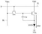
このような各画素は、図1に示したように、スイッチングトランジスタ(Tsw)、駆動トランジスタ(Tdr)、コンデンサ(Cst)、及び有機発光素子(OLED)を含む。 As shown in FIG. 1, each pixel includes a switching transistor (Tsw), a driving transistor (Tdr), a capacitor (Cst), and an organic light emitting device (OLED).
スイッチングトランジスタ(Tsw)は、スキャンライン(SL)に供給されるスキャン信号(S)に基づいてスイッチングされ、データライン(DL)に供給されるデータ電圧(Vdata)を駆動トランジスタ(Tdr)に供給する。 The switching transistor (Tsw) is switched based on the scan signal (S) supplied to the scan line (SL), and supplies the data voltage (Vdata) supplied to the data line (DL) to the drive transistor (Tdr). .
駆動トランジスタ(Tdr)は、スイッチングトランジスタ(Tsw)から供給されるデータ電圧(Vdata)に応じてスイッチングされ、駆動電圧(VDD)によって有機発光素子(OLED)に流れるデータ電流(Ioled)を制御する。 The driving transistor (Tdr) is switched according to the data voltage (Vdata) supplied from the switching transistor (Tsw), and controls the data current (Ioled) flowing through the organic light emitting device (OLED) by the driving voltage (VDD).
コンデンサ(Cst)は、駆動トランジスタ(Tdr)のゲート端子とソース端子との間に接続され、駆動トランジスタ(Tdr)のゲート端子に供給されるデータ電圧(Vdata)に対応する電圧を保存して、保存した電圧で駆動トランジスタ(Tdr)をターンオンさせる。 The capacitor (Cst) is connected between the gate terminal and the source terminal of the driving transistor (Tdr), stores a voltage corresponding to the data voltage (Vdata) supplied to the gate terminal of the driving transistor (Tdr), and The drive transistor (Tdr) is turned on with the stored voltage.
有機発光素子(OLED)は、駆動トランジスタ(Tdr)のソース端子とカソード電圧(VSS)が印加されるカソード電極(CE)との間に電気的に接続され、駆動トランジスタ(Tdr)から供給されるデータ電流(Ioled)によって発光する。 The organic light emitting device (OLED) is electrically connected between the source terminal of the driving transistor (Tdr) and the cathode electrode (CE) to which the cathode voltage (VSS) is applied, and is supplied from the driving transistor (Tdr). Light is emitted by data current (Ioled).
このような一般的な有機発光表示装置の各画素は、データ電圧(Vdata)に応じた駆動トランジスタ(Tdr)のスイッチングを用いて駆動電圧(VDD)によって有機発光素子(OLED)に流れるデータ電流(Ioled)の大きさを制御して、有機発光素子(OLED)を発光させることによって、所定の映像を表示する。 Each pixel of such a general organic light emitting display device uses a switching current of a driving transistor (Tdr) corresponding to a data voltage (Vdata) to drive a data current (OLED) flowing through an organic light emitting device (OLED) by a driving voltage (VDD). By controlling the size of (Ioled) and causing the organic light emitting device (OLED) to emit light, a predetermined image is displayed.
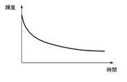
図2は、一般的な有機発光素子の輝度特性を示した図である。 FIG. 2 is a diagram illustrating luminance characteristics of a general organic light emitting device.
図2に示したように、一般的に、有機発光素子は、駆動時間が増加するほど、劣化速度が加速して、輝度特性がだんだん減少することが分かる。したがって、一般的な有機発光表示装置では、時間が経つほど、有機発光素子(OLED)の劣化によって画質が低下するという問題点がある。 As shown in FIG. 2, it can be seen that, in general, the organic light emitting device has a deterioration rate that is accelerated as the driving time is increased, and the luminance characteristic is gradually decreased. Accordingly, a general organic light emitting display device has a problem that the image quality deteriorates as the time elapses due to deterioration of the organic light emitting device (OLED).
一般的に、有機発光表示装置に対する画質補償は、製品が出荷される前に、別途の工程を通じて行われる。しかし、有機発光素子(OLED)は、駆動時間が増加するほど劣化が進行して輝度が減少するので、製品の出荷後に発生する画質の劣化がさらに大きい。 Generally, image quality compensation for an organic light emitting display device is performed through a separate process before the product is shipped. However, organic light emitting devices (OLEDs) degrade as the drive time increases and the brightness decreases, so image quality degradation that occurs after shipment of the product is even greater.
このように、従来の有機発光表示装置は、製品が出荷された後に使用者に、有機発光素子(OLED)の劣化に伴う画質の劣化を補償することができないという問題がある。 As described above, the conventional organic light emitting display device has a problem that the user cannot compensate for the deterioration of the image quality due to the deterioration of the organic light emitting device (OLED) after the product is shipped.
以上、説明した背景技術の内容は、本出願の発明者が本発明の導出のために保有していたか、本発明の導出過程で習得した技術情報であって、必ずしも本発明の出願前に、一般公衆に公開された公知技術であるとは言えない。 The content of the background art described above is technical information that the inventor of the present application has possessed for the derivation of the present invention or has been acquired in the derivation process of the present invention, and is not necessarily prior to the filing of the present invention, It cannot be said that it is a publicly known technique that has been released to the general public.
本発明は、上述した問題点を解決するためのものであって、使用者が画質補償を行うことができる表示装置、光学補償システムおよび光学補償方法を提供することを技術的課題とする。 The present invention is for solving the above-described problems, and an object of the present invention is to provide a display device, an optical compensation system, and an optical compensation method that allow a user to perform image quality compensation.
上述した技術的課題を達成するための本発明の一側面による表示装置は、複数のパターンを順次に表示する表示パネル、および前記複数のパターンのそれぞれに対する輝度データおよび色座標データを外部の使用者が端末装置から受信し、前記受信した輝度データおよび色座標データを用いて補償データを生成する光学補償部を含む。 A display device according to an aspect of the present invention for achieving the above-described technical problem includes a display panel that sequentially displays a plurality of patterns, and luminance data and color coordinate data for each of the plurality of patterns. Includes an optical compensation unit that receives from the terminal device and generates compensation data using the received luminance data and color coordinate data.
上述した技術的課題を達成するための本発明の他の側面による光学補償システムは、輝度および色座標を測定する使用者端末装置、および複数のパターンを順次に表示して、前記複数のパターンのそれぞれの輝度データおよび色座標データを前記使用者の端末装置から受信し、前記受信した輝度データおよび色座標データを用いて補償データを作成し、保存する表示装置を含む。 An optical compensation system according to another aspect of the present invention for achieving the above-described technical problem includes a user terminal device that measures luminance and color coordinates, and a plurality of patterns sequentially displayed, and the plurality of patterns. A display device that receives each luminance data and color coordinate data from the user's terminal device, generates compensation data using the received luminance data and color coordinate data, and stores the compensation data.
上述した技術的課題を達成するための本発明のまた他の側面による表示装置の光学補償方法は、映像表示モードでは、初期設定データを用いて映像を表示する工程と、前記映像表示モードから光学補償モードに変更されると、複数のパターンを順次に表示して、前記複数のパターンのそれぞれに対する輝度データおよび色座標データを外部の使用者端末装置から受信し、前記受信した輝度データおよび色座標データを用いて補償データを生成して保存する工程、および前記光学補償モードが完了し、前記映像表示モードに変更されると、前記補償データを用いて映像を表示する工程を含む。 An optical compensation method for a display device according to still another aspect of the present invention for achieving the technical problem described above includes a step of displaying an image using initial setting data in an image display mode, and an optical from the image display mode. When the compensation mode is changed, a plurality of patterns are sequentially displayed, and luminance data and color coordinate data for each of the plurality of patterns are received from an external user terminal device, and the received luminance data and color coordinates are received. Generating and storing compensation data using the data, and displaying the image using the compensation data when the optical compensation mode is completed and changed to the image display mode.
本発明によれば、製品出荷後も使用者が端末装置を用いて画質の劣化を補償することができるという効果がある。 According to the present invention, there is an effect that the user can compensate for the deterioration of the image quality using the terminal device even after the product is shipped.
また、本発明によれば、使用者が画質の低下なしに、継続的に高画質の映像を視聴することができるという別の効果がある。 In addition, according to the present invention, there is another effect that the user can continuously view high-quality video without lowering the image quality.
本明細書で記述される用語の意味は、次にように理解されなければならない。 The meaning of the terms described herein should be understood as follows.
単数の表現は、文脈上明らかに別の方法で定義しない限り、複数の表現を含むものと理解されなければならず、「第1」、「第2」などの用語は、一つの構成要素を他の構成要素から区別するためのもので、これらの用語によって権利範囲が限定されてはならない。 A singular expression must be understood to include a plurality of expressions unless the context clearly defines otherwise, and terms such as "first" and "second" refer to a single component. They are intended to distinguish them from other components, and the scope of rights should not be limited by these terms.
「含む」または「有する」などの用語は、一つまたはそれ以上の他の特徴や数字、工程、動作、構成要素、部分品またはそれらを組み合わせたものの存在または付加の可能性を事前に排除しないものと理解されなければならない。 Terms such as “include” or “have” do not pre-exclude the possibility of the presence or addition of one or more other features or numbers, steps, actions, components, components or combinations thereof. It must be understood.
「少なくとも一つ」の用語は、一つまたは複数の関連項目から提示可能なすべての組み合わせを含むものと理解されなければならない。例えば、「第1項目、第2項目及び第3項目の中から少なくとも一つ」の意味は、第1項目、第2項目または第3項目のそれぞれと同様に、第1項目、第2項目及び第3項目の中から2以上から提示することができるすべての項目の組み合わせを意味する。 The term “at least one” should be understood to include all combinations that can be presented from one or more related items. For example, the meaning of “at least one of the first item, the second item, and the third item” is the same as the first item, the second item, and the third item, respectively. It means a combination of all items that can be presented from two or more of the third items.
「上に」という用語は、ある構成が他の構成のすぐ上面に形成される場合だけでなく、それらの構成の間に第3の構成が介在する場合まで含まれ得ることを意味する。 The term “on” means that a configuration can be included not only when it is formed immediately above another configuration, but also when a third configuration is interposed between those configurations.
以下では、図を参照して、本発明に係る好適な実施例に対して詳細に説明することにする。 The preferred embodiments of the present invention will be described in detail below with reference to the drawings.
図3は、本発明の一実施例に係る光学補償システムを概略的に示した図である。 FIG. 3 is a diagram schematically showing an optical compensation system according to an embodiment of the present invention.
図3を参照すると、本発明の一実施例に係る光学補償システム100は、表示装置110および使用者端末装置120を含む。 Referring to FIG. 3, the
まず、表示装置110は、映像表示モードおよび光学補償モードのいずれかで動作する。表示装置110は、映像表示モードでは、使用者が視聴しようとする映像を表示する。 First, the
映像表示モードから光学補償モードに変更されると、表示装置110は、光学補償のために事前に保存しておいた複数のパターンを順次に表示する。そして、表示装置110は、各パターンに対する輝度データおよび色座標データを使用者端末装置120から受信して補償データを生成および保存する。 When the video display mode is changed to the optical compensation mode, the
以後、表示モードに変更されると、表示装置110は、光学補償モードで生成した補償データを用いて映像を表示する。 Thereafter, when the display mode is changed, the
次に、使用者端末装置120は、映像表示モードおよび光学補償モードのいずれかで動作する。使用者端末装置120は、映像表示モードでは、使用者の入力によって発生した制御信号を表示装置110に送信する。これにより、使用者端末装置120は、表示装置110に表示される映像を制御することができる。 Next, the
使用者端末装置120は、光学補償モードで表示装置110から光学補償情報が要請されると、表示装置110に表示されたパターンに対する輝度および色座標を測定する。そして、使用者端末装置120は、輝度データおよび色座標データを生成して表示装置110に送信する。 When optical compensation information is requested from the
図4は図3の表示装置を示した図であり、図5は図4の表示パネルおよびパネル駆動部を詳細に説明するための図である。 4 is a diagram showing the display device of FIG. 3, and FIG. 5 is a diagram for explaining the display panel and the panel driving unit of FIG. 4 in detail.
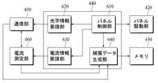
図4を参照すると、本発明の一実施例に係る表示装置110は、表示パネル410、パネル駆動部420、メモリ430、光学補償部440、通信部450、電流測定部460および動作モード制御部470を含む。 Referring to FIG. 4, a
まず、表示パネル410は、パネル駆動部420によって映像またはパターンを表示する。より詳細には、表示装置110が映像表示モードで動作すると、表示パネル410は、パネル駆動部420によって映像を表示する。一方、表示装置110が光学補償モードで動作すると、表示パネル410は、パネル駆動420によって、複数のパターンを順次に表示する。 First, the
このような表示パネル410は、図5に示したように、複数のスキャンライン(SL)、複数のセンシングライン(SS)、複数のデータライン(DL)、複数の駆動電圧ライン(PL)、複数の基準電圧ライン(RL)および、複数の画素(P)を含む。 As shown in FIG. 5, the
複数のデータライン(DL)は、複数のスキャンライン(SL)および、複数のセンシングライン(SS)と交差することができる。複数のスキャンライン(SL)と、複数のセンシングライン(SS)は、互いに並んで形成され得る。 The plurality of data lines (DL) can intersect with the plurality of scan lines (SL) and the plurality of sensing lines (SS). The plurality of scan lines (SL) and the plurality of sensing lines (SS) may be formed side by side.
そして、複数の画素(P)のそれぞれは、赤色画素、緑色画素、青色画素、および白色画素のいずれか一つからなり得る。また、赤色画素、緑色画素、青色画素、および白色画素は、一つの単位画素と定義することができる。各画素(P)は、データライン(DL)のいずれか一つ、駆動電圧ライン(PL)のいずれか一つ、および基準電圧ライン(RL)のいずれか一つに接続することができる。 Each of the plurality of pixels (P) may be composed of any one of a red pixel, a green pixel, a blue pixel, and a white pixel. Further, the red pixel, the green pixel, the blue pixel, and the white pixel can be defined as one unit pixel. Each pixel (P) can be connected to any one of the data lines (DL), any one of the drive voltage lines (PL), and any one of the reference voltage lines (RL).
画素(P)は、データライン(DL)からデータ電圧が供給され、データ電圧に応じて、有機発光素子(OLED)に電流を供給する。これにより、画素(P)は、所定の輝度で発光する。画素(P)の構造の詳細な説明は、図1で説明したので省略する。 The pixel (P) is supplied with a data voltage from the data line (DL), and supplies a current to the organic light emitting device (OLED) according to the data voltage. Thereby, the pixel (P) emits light with a predetermined luminance. The detailed description of the structure of the pixel (P) has been described with reference to FIG.
次に、パネル駆動部420は、映像データまたはパターンデータが入力すると、表示パネル410に映像データに相応する映像、またはパターンデータに相応するパターンが表示されるように表示パネル410を駆動する。 Next, when the video data or the pattern data is input, the
このようなパネル駆動部420は、図5に示したように、データ駆動部422、スキャン駆動部424およびタイミング制御部426を含む。 The
スキャン駆動部424は、複数のスキャンライン(SL)に接続され、スキャン信号を供給する。スキャン駆動部424は、タイミング制御部426から入力するタイミングスキャン制御信号に応じて、複数のスキャンライン(SL)にスキャン信号を供給する。スキャン駆動部424は、複数のスキャンライン(SL)にスキャン信号を順次に供給することができ、この場合、シフトレジスタを含むことができる。 The
スキャン駆動部424は、集積回路(integrated circuit)のような駆動チップ(chip)に形成して表示パネル410に付着される軟性フィルム上に実装したり、複数のトランジスタを含み、GIP(Gate driver In Panel)方法で表示パネル410の非表示領域に直接形成することができる。 The
データ駆動部422は、複数のデータライン(DL)に接続して、データ電圧を供給する。データ駆動部422は、タイミング制御部426からタイミングデータ制御信号および補償データが入力する。データ駆動部422は、補償データをデータ電圧に変換してデータライン(DL)に供給する。ここで、データ電圧は、画素(P)の有機発光素子(OLED)が所定の輝度で発光するための電圧である。データ駆動部422に供給される補償データが8ビットである場合、データ電圧のそれぞれは、256個の電圧のうちいずれか一つで供給することができる。 The
このようなデータ駆動部422は、集積回路のような駆動チップに形成して表示パネル410に付着される軟性フィルム上に実装したり、表示パネル410上に直接接着することができる。 The
タイミング制御部426は、スキャン駆動部424および、データ駆動部422の動作タイミングを制御するためのタイミング制御信号を生成する。タイミング制御信号は、データ駆動部422の動作タイミングを制御するためのデータタイミング制御信号、およびスキャン駆動部424の動作タイミングを制御するためのスキャンタイミング制御信号を含む。 The
タイミング制御部426は、外部から映像データの入力を受けたり、光学補償部440からパターンデータが入力する。タイミング制御部426は、メモリ430に保存されているデータを用いて映像データまたはパターンデータを補正データに補正する。 The
光学補償が行われる前、メモリ430は、製品出荷前に設定された初期設定データを保存している。ここで、タイミング制御部426は、映像データが入力すると、初期設定データを用いて映像データを補正データに補正する。 Before optical compensation is performed, the
そして、光学補償が行われた後、メモリ430は、有機発光素子(OLED)の劣化を補償するための補償データを保存している。ここで、タイミング制御部426は、映像データが入力すると、補償データを用いて映像データを補正データに補正することにより、有機発光素子(OLED)の劣化を補償することができる。 Then, after optical compensation is performed, the
次に、メモリ430は、初期設定データまたは補償データを保存する。ここで、初期設定データは、表示装置110が出荷される前に、初期光学補償工程によって設定されてメモリ430に保存されているものである。 Next, the
メモリ430は、製品が出荷されるときに、初期設定データを保存しているが、後に光学補償部440によって補償データが生成されると、補償データを保存する。 The
次に、光学補償部440は、動作モード制御部270から光学補償制御信号が入力する。光学補償部440は、光学補償制御信号に応じて光学補償モードで動作して、有機発光素子(OLED)の劣化を補償するための補償データを生成する。 Next, the
特に、本発明は、外部の使用者端末装置120からの光学情報を受信して補償データを生成することを特徴とする。以下では、図6を参照して、光学補償部440に対して、より詳細に説明する。 In particular, the present invention is characterized in that it receives optical information from an external
図6は、図4の光学補償部を説明するための図である。 FIG. 6 is a diagram for explaining the optical compensator of FIG.
図6を参照すると、光学補償部440は、パターン制御部610、光学情報要請部620、電流情報要請部630及び補償データ生成部640を含む。 Referring to FIG. 6, the
まず、パターン制御部610は、動作モード制御部470によって光学補償モードで動作すると、複数のパターンのそれぞれに対するパターンデータをパネル駆動部420に順次に出力する。 First, when the operation
前記複数のパターンは、有機発光素子(OLED)の劣化に伴う輝度および色座標の変化を測定するためのものであって、表示装置110に予め保存されている。このような複数のパターンは、複数のデータ電圧に対応するパターンを含む。例えば、複数のパターンは、256個のデータ電圧のそれぞれに対応するパターンを含み、パターン制御部610は、各パターンのパターンデータをパネル駆動部420に順次に出力することができる。 The plurality of patterns are for measuring changes in luminance and color coordinates due to deterioration of the organic light emitting device (OLED), and are stored in the
また、複数のパターンは、色、形、および大きさのうちの少なくとも一つが互いに異なることを特徴とする。 The plurality of patterns may be different from each other in at least one of color, shape, and size.
例えば、パターン制御部610は、色が異なる複数のパターンのパターンデータをパネル駆動部420に順次に出力することができる。表示パネル410は、図7に示したように、パネル駆動部420によって、画面のすべての黒色、赤色、緑色、青色、白色を順次に表示することができる。 For example, the
他の例として、パターン制御部610は、大きさが異なる複数のパターンに対するパターンデータをパネル駆動部420に順次に出力することができる。表示パネル410は、図8に示したように、パネル駆動部420によって大きさが異なる四角パターンを順次に表示することができる。 As another example, the
また、複数のパターンは、表示装置110全部に黒色を表示する黒色パターンを含む。黒色パターンは、使用者端末装置120で環境補正値を算出するためのものであって、光学補償モードが開始されると、最初に表示される。これに対する詳細な内容は、図9で、使用者端末装置120と一緒に説明することにする。 The plurality of patterns include a black pattern that displays black on the
一方、パターン制御部610は、複数のパターンのうちいずれか一つのパターンデータをパネル駆動部420に出力しながら、光学情報要請部620を通じて外部の使用者端末装置120に光学情報を要請する。 Meanwhile, the
また、パターン制御部610は、複数のパターンのうちのいずれか一つのパターンデータをパネル駆動部420に出力しながら、電流情報要請部630を通じて電流測定部460に表示パネル410に対する電流情報を要請する。 In addition, the
次に、補償データ生成部640は、表示パネル410に示されたパターンに対する光学情報および電流情報を用いて有機発光素子(OLED)の劣化を補償するための補償データを生成する。 Next, the compensation
より詳細には、補償データ生成部640は、通信部450を通じてパターンに対する光学情報が入力する。ここで、光学情報は、表示パネル410に表示されたパターンに対する輝度データおよび色座標データを含む。 More specifically, the compensation
そして、補償データ生成部640は、電流測定部460から電流情報が入力する。ここで、電流情報は、表示パネル410にパターンが表示される時に表示パネル410に流れる電流データを含む。 The compensation
そして、補償データ生成部640は、パターン制御部610から表示パネル410に表示されたパターンに対するパターンデータが入力する。 The compensation
補償データ生成部640は、表示パネル410に表示されたパターンに対するパターンデータ、輝度データ、色座標データおよび電流データを用いて有機発光素子(OLED)の劣化を補償するための補償データを生成する。補償データ生成部640は、所定のアルゴリズムを用いて、パターンデータ、輝度データ、色座標データおよび電流データから補償データを算出することができる。 The compensation
そして、補償データ生成部640は、生成された補償データをメモリ430に保存する。メモリ430には、製品が出荷される前に保存された初期設定データが保存されているが、補償データ生成部640は、前記初期設定データを補償データに変更および保存する。 Then, the compensation
再び図4を参照すると、通信部450は、外部の使用者端末装置120と無線または有線で通信する。通信部450は、使用者端末装置120に光学情報の要請を送信して、要請に応じた光学情報を受信する。 Referring to FIG. 4 again, the
次に、電流測定部460は、表示パネル410に流れる電流を測定し、測定された電流に対応する電流データを補償データ生成部640に提供する。 Next, the
次に、動作モード制御部470は、表示装置110に対する動作モードを制御する。 Next, the operation
動作モード制御部470は、表示装置110に対する動作モードで表示モードおよび光学補償モードのいずれか一つを決定する。動作モード制御部470は、表示装置110に対する動作モードで表示モードが決定されると、パネル駆動部420が、外部から映像データの入力を受けるよう制御する。 The operation
一方、動作モード制御部470は、使用者端末装置120から光学補償要請を受信したり、所定の時間が経過すると表示装置110に対する動作モードを表示モードから光学補償モードに変更する。 On the other hand, the operation
動作モード制御部470は、使用者端末装置120から光学補償要請を受信することができる。つまり、使用者は、表示装置110に対して光学補償が必要であると判断した場合、使用者端末装置120を通じて表示装置110に光学補償を要請することができる。動作モード制御部470は、使用者端末装置120から光学補償要請を受信すると、表示装置110に対する動作モードを表示モードから光学補償モードに変更して、表示装置110に対する光学補償を実行することができる。 The operation
また、動作モード制御部470は、所定の時間が経過すると表示装置110に対する動作モードを表示モードから光学補償モードに変更して、光学補償を開始することができる。ここで、所定の時間は、有機発光素子(OLED)の劣化速度を考慮して、あらかじめ設定したり、使用者端末装置120を通じて使用者が直接設定することができる。例えば、動作モード制御部470は、1年周期で表示装置110に対する動作モードを表示モードから光学補償モードに変更して、表示装置110に対する光学補償を行うことができる。 In addition, the operation
図9は、図3の使用者端末装置を示した図である。 FIG. 9 is a diagram showing the user terminal device of FIG.
図9を参照すると、本発明の一実施例に係る使用者端末装置120は、測定部910、環境補正値決定部920、データ補正部930および通信部940を含む。 Referring to FIG. 9, a
まず、測定部910は、表示装置110から光学情報の要請を受信すると、表示装置110に示されたパターンに対する輝度および色座標を測定する。 First, when receiving a request for optical information from the
一実施例において、測定部910は、受光素子、および前記受光素子上に形成されたカラーフィルタ(color filter)で構成することができる。測定部910は、表示装置110から入射するパターンの光をカラーフィルターを通過させて色を分離することができる。そして、測定部910は、受光素子を通じて色が分離された光を吸収して色座標および輝度を測定することができる。 In one embodiment, the measuring
次に、環境補正値決定部920は、外部光および測定装置の誤差などの環境要因を考慮して、環境補正値を決定する。 Next, the environmental correction
このような環境補正値決定部920は、黒色パターンに対する輝度をもとに、環境補正値を決定する。前記黒色パターンに対する輝度が0でなければならないが、輝度測定部910は、外部光または測定装置の誤差によって黒色パターンに対する輝度が0より大きく測定される。このような誤差を減らすために、環境補正値決定部920は、表示装置110に黒色パターンが表示される時に測定した輝度値に基づいて環境補正値を決定する。 Such an environmental correction
次に、データ補正部930は、環境補正値を用いて、輝度データおよび色座標データを補正する。データ補正部930は、輝度測定部910によって測定された輝度値に環境補正値を減算して輝度データを補正する。 Next, the
次に、通信部940は、表示装置110と無線または有線で通信する。通信部940は、表示装置110から光学情報の要請を受信し、要請に対する光学情報、より詳細には、データ補正部930によって補正された輝度データおよび色座標データを表示装置110に送信する。 Next, the
図10は、本発明の一実施例に係る表示装置で光学補償を実行する方法を説明する流れ図である。 FIG. 10 is a flowchart illustrating a method for performing optical compensation in a display device according to an embodiment of the present invention.
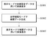
図10を参照すると、本発明の一実施例に係る表示装置110は、表示モードでは、初期設定データを用いて映像を表示する(S1001)。 Referring to FIG. 10, the
より詳細には、外部から映像データが入力すると、パネル駆動部420は、入力した映像データをメモリ430に保存された初期設定データを用いて、補正データに補正する。そして、パネル駆動部420は、補正データをデータ電圧に変換してデータライン(DL)に供給する。ここで、表示パネル410は、データライン(DL)から供給されるデータ電圧に応じて所定の輝度で発光することにより、映像を表示する。 More specifically, when video data is input from the outside, the
次に、表示装置110は、使用者端末装置120から光学補償要請を受信したり、所定の時間が経過すると、動作モードを表示モードから光学補償モードに変更する。そして、表示装置110は、有機発光素子(OLED)の劣化を補償するための補償データを生成する(S1002)。 Next, the
以下では、図11を参照して、補償データを生成する方法に対して、より詳細に説明する。 Hereinafter, a method for generating compensation data will be described in more detail with reference to FIG.
図11は、本発明の一実施例に係る表示装置で補償データを生成する方法を説明する流れ図である。 FIG. 11 is a flowchart illustrating a method for generating compensation data in a display device according to an embodiment of the present invention.
図11を参照すると、本発明の一実施例に係る表示装置110は、動作モードが表示モードから光学補償モードに変更されると、表示パネル410に第1のパターンを表示する(S1101)。ここで、第1のパターンは、黒色パターンに相応し得る。 Referring to FIG. 11, the
より詳細には、光学補償部440は、パネル駆動部420に第1のパターンに対応する第1のパターンデータを出力する。パネル駆動部420は、入力した第1のパターンデータをデータ電圧に変換してデータライン(DL)に供給する。ここで、表示パネル410は、データライン(DL)から供給されるデータ電圧に応じて所定の輝度で発光することにより、第1のパターンを表示する。 More specifically, the
他の実施例では、パネル駆動部420は、入力した第1のパターンデータをメモリ430に保存された初期設定データを用いて、補正データに補正することができる。そして、パネル駆動部420は、補正データをデータ電圧に変換してデータライン(DL)に供給することができる。ここで、表示パネル410は、データライン(DL)から供給されるデータ電圧に応じて所定の輝度で発光することにより、映像を表示することができる。 In another embodiment, the
次に、表示装置110は、使用者端末装置120に光学情報を要請し、要請に応じた光学情報を受信する(S1102およびS1103)。ここで、光学情報は、第1のパターンに対する輝度データおよび色座標データを含む。 Next, the
そして、表示装置110は、第1のパターンが表示された表示パネル410に流れる電流を測定し、測定された電流に対応する電流データを生成する(S1104およびS1105)。 Then, the
次に、表示装置110は、所定のアルゴリズムを用いて、パターンデータ、輝度データ、色座標データ、および電流データから補償データを算出する(S1106)。 Next, the
次に、表示装置110は、残りのパターンに対してS1101からS1106を繰り返し実行する(S1107およびS1108)。 Next, the
次に、表示装置110は、複数のパターンに対して補償データが生成されると、生成された補償データをメモリ430に保存する(S1109)。 Next, when the compensation data is generated for a plurality of patterns, the
再び図10を参照すると、表示装置110は、光学補償が完了すると、動作モードが光学補償モードから表示モードに変更される。そして、表示装置110は、表示モードで補償データを用いて映像を表示する(S1003)。 Referring to FIG. 10 again, when the optical compensation is completed, the operation mode of the
より詳細には、外部から映像データが入力されると、パネル駆動部420は、入力された映像データをメモリ430に保存された補償データを用いて、補正データに補正する。そして、パネル駆動部420は、補正データをデータ電圧に変換してデータライン(DL)に供給する。ここで、表示パネル410は、データライン(DL)から供給されるデータ電圧に応じて所定の輝度で発光することにより、映像を表示する。 More specifically, when video data is input from the outside, the
図12は、本発明の一実施例に係る使用者端末装置で光学補償を実行する方法を説明する流れ図である。 FIG. 12 is a flowchart illustrating a method for performing optical compensation in a user terminal device according to an embodiment of the present invention.
図12を参照すると、本発明の一実施例に係る使用者端末装置120は、表示装置110から第1のパターンに対する光学情報の要請を受信すると、表示装置110に表示された第1のパターンに対する輝度および色座標を測定する(S1201およびS1202)。ここで、第1のパターンは、表示装置110の表示領域全体に黒色が表示される黒色パターンに対応する。 Referring to FIG. 12, when the
次に、使用者端末装置120は、第1のパターンに対して測定した輝度値および色座標値を用いて、環境補正値を決定する(S1203)。 Next, the
次に、使用者端末装置120は、環境補正値を用いて前記測定した輝度値および色座標値を補正して、補正した輝度値および色座標値に対応する輝度データおよび色座標データを生成する(S1204)。 Next, the
次に、使用者端末装置120は、輝度データおよび色座標データを表示装置110に送信する(S1205)。 Next, the
次に、使用者端末装置120は、表示装置110から第2のパターンの光学情報に対する要請を受信すると、表示装置110に表示された第2のパターンに対する輝度および色座標を測定する(S1206およびS1207) 。 Next, when the
次に、使用者端末装置120は、第2のパターンに対して測定した輝度値および色座標値を環境補正値を用いて補正して、補正した輝度値および色座標値に対応する輝度データおよび色座標データを生成する(S1208)。 Next, the
次に、使用者端末装置120は、輝度データおよび色座標データを表示装置110に送信する(S1209)。 Next, the
次に、使用者端末装置120は、光学補償が完了するまでS1206からS1209を繰り返し実行する。 Next, the
以上で説明した本発明は、前述した実施例及び添付した図に限定されるものではなく、本発明の技術的事項を逸脱しない範囲内で様々な置換、変形及び変更が可能であることが、本発明が属する技術分野で通常の知識を有する者にとって明らかであろう。したがって、本発明の範囲は、後述する特許請求の範囲によって示され、特許請求の範囲の意味および範囲そしてその等価概念から導出されるすべての変更または変形された形態が本発明の範囲に含まれるものと解釈されなければならない。 The present invention described above is not limited to the above-described embodiments and attached drawings, and various substitutions, modifications and changes can be made without departing from the technical matters of the present invention. It will be apparent to those skilled in the art to which the present invention belongs. Therefore, the scope of the present invention is indicated by the scope of claims described later, and all modifications or variations derived from the meaning and scope of the claims and equivalents thereof are included in the scope of the present invention. Must be interpreted.
100:光学補償システム
110:表示装置
120:使用者端末装置
410:表示パネル
420:パネル駆動部
430:メモリ
440:光学補償部
450:通信部
460:電流測定部
470:動作モード制御部
610:パターン制御部
620:光学情報要請部
630:電流情報要請部
640:補償データ生成部
910:測定部
920:環境補正値決定部
930:データ補正部
940:通信部DESCRIPTION OF SYMBOLS 100: Optical compensation system 110: Display apparatus 120: User terminal device 410: Display panel 420: Panel drive part 430: Memory 440: Optical compensation part 450: Communication part 460: Current measurement part 470: Operation mode control part 610: Pattern Control unit 620: Optical information request unit 630: Current information request unit 640: Compensation data generation unit 910: Measurement unit 920: Environmental correction value determination unit 930: Data correction unit 940: Communication unit
Claims (11)
Translated fromJapanese前記複数のパターンのそれぞれの輝度データおよび色座標データを外部の使用者端末装置から受信し、前記受信した輝度データおよび色座標データを用いて補償データを生成する光学補償部を含む表示装置。A display panel for sequentially displaying a plurality of patterns, and brightness data and color coordinate data of each of the plurality of patterns are received from an external user terminal device, and compensation data is received using the received brightness data and color coordinate data A display device including an optical compensation unit that generates
映像データが入力すると、前記補償データを用いて前記映像データを補正データに補正して、前記補正データをデータ電圧に変換して前記表示パネルに印加するパネル駆動部を含む請求項1に記載の表示装置。The display device
The display apparatus according to claim 1, further comprising: a panel driver that, when video data is input, corrects the video data to correction data using the compensation data, converts the correction data into a data voltage, and applies the data to the display panel. Display device.
前記表示パネルに流れる電流を測定し、前記測定された電流に対応する電流データを前記光学補償部に出力する電流測定部をさらに含むことを特徴とする請求項1から4のいずれか一項に記載の表示装置。The display device
5. The apparatus according to claim 1, further comprising a current measurement unit that measures a current flowing through the display panel and outputs current data corresponding to the measured current to the optical compensation unit. The display device described.
前記電流測定部から前記複数のパターンのそれぞれに対する電流データの入力を受けて、前記輝度データ、前記色座標データ、および前記電流データを用いて補償データを生成することを特徴とする請求項5に記載の表示装置。The optical compensation unit is
6. The compensation data is generated using the luminance data, the color coordinate data, and the current data in response to input of current data for each of the plurality of patterns from the current measuring unit. The display device described.
複数のパターンを順次に表示して、前記複数のパターンのそれぞれに対する輝度データおよび色座標データを前記使用者端末装置から受信し、前記受信した輝度データおよび色座標データを用いて補償データを生成および保存する表示装置を含む光学補償システム。A user terminal device that measures luminance and color coordinates, and a plurality of patterns are sequentially displayed, luminance data and color coordinate data for each of the plurality of patterns are received from the user terminal device, and the received luminance An optical compensation system including a display device that generates and stores compensation data using data and color coordinate data.
受光素子、前記受光素子上に形成されたカラーフィルタ、および前記表示装置に表示されたパターンの光を吸収して輝度および色座標を測定する測定部を含むことを特徴とする請求項7に記載の光学補償システム。The user terminal device is
The light receiving element, a color filter formed on the light receiving element, and a measurement unit that absorbs light of a pattern displayed on the display device and measures luminance and color coordinates. Optical compensation system.
黒色パターンに対する輝度を用いて、環境補正値を決定し、測定された輝度および色座標を前記環境補正値を用いて補正することを特徴とする請求項7または8に記載の光学補償システム。The user terminal device is
9. The optical compensation system according to claim 7, wherein an environmental correction value is determined using the luminance with respect to the black pattern, and the measured luminance and color coordinates are corrected using the environmental correction value.
前記複数のパターンを順次に表示する表示パネル、および
前記表示パネルに流れる電流を測定し、前記測定された電流に対応する電流データ、前記受信した輝度データ、及び前記色座標データを用いて補償データを生成する光学補償部を含むことを特徴とする請求項7から9のいずれか一項に記載の光学補償システム。The display device
A display panel that sequentially displays the plurality of patterns, and a current flowing through the display panel is measured, and compensation data is obtained using the current data corresponding to the measured current, the received luminance data, and the color coordinate data. The optical compensation system according to claim 7, further comprising an optical compensation unit that generates
前記映像表示モードから光学補償モードに変更されると、複数のパターンを順次に表示して、前記複数のパターンのそれぞれに対する輝度データおよび色座標データを外部の使用者端末装置から受信し、前記受信した輝度データおよび色座標データを用いて補償データを生成して保存する工程と、および
前記光学補償モードが完了し、前記映像表示モードに変更されると、前記補償データを用いて映像を表示する工程を含む表示装置の光学補償方法。In the video display mode, a process of displaying video using the initial setting data;
When the image display mode is changed to the optical compensation mode, a plurality of patterns are sequentially displayed, and luminance data and color coordinate data for each of the plurality of patterns are received from an external user terminal device, and the reception Generating and storing compensation data using the luminance data and color coordinate data, and displaying the video using the compensation data when the optical compensation mode is completed and changed to the video display mode. An optical compensation method for a display device including the steps.
Applications Claiming Priority (2)
| Application Number | Priority Date | Filing Date | Title |
|---|---|---|---|
| KR10-2015-0191135 | 2015-12-31 | ||
| KR1020150191135AKR102437049B1 (en) | 2015-12-31 | 2015-12-31 | Display device, optical compensation system and optical compensation method thereof |
Publications (2)
| Publication Number | Publication Date |
|---|---|
| JP2017120421Atrue JP2017120421A (en) | 2017-07-06 |
| JP6472783B2 JP6472783B2 (en) | 2019-02-20 |
Family
ID=59227099
Family Applications (1)
| Application Number | Title | Priority Date | Filing Date |
|---|---|---|---|
| JP2016253326AActiveJP6472783B2 (en) | 2015-12-31 | 2016-12-27 | Display device, optical compensation system, and optical compensation method |
Country Status (5)
| Country | Link |
|---|---|
| US (1) | US10672344B2 (en) |
| JP (1) | JP6472783B2 (en) |
| KR (1) | KR102437049B1 (en) |
| CN (1) | CN106935196B (en) |
| TW (1) | TWI615828B (en) |
Cited By (1)
| Publication number | Priority date | Publication date | Assignee | Title |
|---|---|---|---|---|
| WO2020136731A1 (en)* | 2018-12-25 | 2020-07-02 | 堺ディスプレイプロダクト株式会社 | Correction image generation system, image control method, image control program, and recording medium |
Families Citing this family (7)
| Publication number | Priority date | Publication date | Assignee | Title |
|---|---|---|---|---|
| KR102437049B1 (en)* | 2015-12-31 | 2022-08-25 | 엘지디스플레이 주식회사 | Display device, optical compensation system and optical compensation method thereof |
| WO2018167884A1 (en)* | 2017-03-15 | 2018-09-20 | シャープ株式会社 | Organic electroluminescence display device and drive method therefor |
| CN107799066B (en)* | 2017-11-15 | 2020-04-07 | 京东方科技集团股份有限公司 | Compensation method of display panel, driving device, display device and storage medium |
| CN109523955B (en)* | 2019-01-03 | 2020-07-07 | 京东方科技集团股份有限公司 | Pixel compensation method and device, storage medium and display screen |
| KR102650708B1 (en)* | 2020-03-20 | 2024-03-25 | 삼성디스플레이 주식회사 | Display apparatus and method of driving the same |
| KR102801929B1 (en) | 2020-05-19 | 2025-05-07 | 삼성디스플레이 주식회사 | Display device and luminance profile measurement method |
| KR102742944B1 (en) | 2020-08-12 | 2024-12-17 | 삼성디스플레이 주식회사 | Display system and method of compensating image of display panel using the same |
Citations (11)
| Publication number | Priority date | Publication date | Assignee | Title |
|---|---|---|---|---|
| JP2004228645A (en)* | 2003-01-20 | 2004-08-12 | Konica Minolta Holdings Inc | Solid-state imaging apparatus and optical apparatus using the same |
| JP2004228948A (en)* | 2003-01-23 | 2004-08-12 | Seiko Epson Corp | Image processing system, projector, program, information storage medium, and image processing method |
| US20040183759A1 (en)* | 2002-09-09 | 2004-09-23 | Matthew Stevenson | Organic electronic device having improved homogeneity |
| JP2007140534A (en)* | 2006-12-04 | 2007-06-07 | Sony Corp | Device and method for creating coefficient data, program for performing the method, and computer-readable medium with the program recorded |
| WO2008059637A1 (en)* | 2006-11-16 | 2008-05-22 | Sharp Kabushiki Kaisha | Image display apparatus and image display method |
| WO2008068920A1 (en)* | 2006-12-06 | 2008-06-12 | Sharp Kabushiki Kaisha | Gradation voltage correction system and display apparatus utilizing the same |
| JP2009134142A (en)* | 2007-11-30 | 2009-06-18 | Kyocera Corp | Conversion rule setting method and image display device |
| JP2011053634A (en)* | 2009-09-04 | 2011-03-17 | Panasonic Corp | Display device, method of manufacturing the same, method of correcting, and display evaluating device |
| US20120074851A1 (en)* | 2010-09-23 | 2012-03-29 | Dolby Laboratories Licensing Corporation | Method and System for Display Calibration with Feedback Determined by a Camera Device |
| US20140055500A1 (en)* | 2012-08-23 | 2014-02-27 | Research In Motion Limited | Organic light emitting diode based display aging monitoring |
| US20150317944A1 (en)* | 2014-05-02 | 2015-11-05 | Qualcomm Incorporated | Mobile device based color management of digital displays |
Family Cites Families (36)
| Publication number | Priority date | Publication date | Assignee | Title |
|---|---|---|---|---|
| KR930005599B1 (en)* | 1991-05-16 | 1993-06-23 | 삼성전자 주식회사 | Apparatus and method for adjusting tv screen for color tv set |
| US7728845B2 (en)* | 1996-02-26 | 2010-06-01 | Rah Color Technologies Llc | Color calibration of color image rendering devices |
| US20060007239A1 (en)* | 2004-07-06 | 2006-01-12 | Harrison Charles F | Color correction system |
| TW200631432A (en)* | 2005-02-21 | 2006-09-01 | Asustek Comp Inc | Display system and displaying method capable of auto-adjusting display brightness |
| JP4059910B2 (en)* | 2005-11-11 | 2008-03-12 | シャープ株式会社 | Liquid crystal display |
| US8406562B2 (en)* | 2006-08-11 | 2013-03-26 | Geo Semiconductor Inc. | System and method for automated calibration and correction of display geometry and color |
| US20100201275A1 (en) | 2009-02-06 | 2010-08-12 | Cok Ronald S | Light sensing in display device |
| KR101612455B1 (en)* | 2009-04-16 | 2016-04-15 | 삼성디스플레이 주식회사 | Method of correcting pixel data, and display apparatus for performing the method |
| US20120062621A1 (en) | 2009-08-28 | 2012-03-15 | Mitsubishi Electric Corporation | Brightness adjusting device |
| JP5577812B2 (en)* | 2010-04-15 | 2014-08-27 | セイコーエプソン株式会社 | Image processing apparatus, display system, electronic apparatus, and image processing method |
| CN102376245B (en) | 2010-08-06 | 2014-02-05 | 瑞轩科技股份有限公司 | Optical feedback control system and optical feedback control method of display device |
| US8836796B2 (en)* | 2010-11-23 | 2014-09-16 | Dolby Laboratories Licensing Corporation | Method and system for display characterization or calibration using a camera device |
| US8619103B2 (en) | 2011-01-31 | 2013-12-31 | Global Oled Technology Llc | Electroluminescent device multilevel-drive chromaticity-shift compensation |
| KR101853065B1 (en)* | 2011-03-23 | 2018-04-30 | 삼성디스플레이 주식회사 | Luminance Correction System for Organic Light Emitting Display Device and Luminance Correction method thereof |
| KR20130051576A (en)* | 2011-11-10 | 2013-05-21 | 삼성전자주식회사 | Optimizing method of visibility and system thereof, portable device using the same |
| KR101272367B1 (en)* | 2011-11-25 | 2013-06-07 | 박재열 | Calibration System of Image Display Device Using Transfer Functions And Calibration Method Thereof |
| US9076252B2 (en)* | 2012-01-05 | 2015-07-07 | Qualcomm Incorporated | Image perceptual attribute adjustment |
| US9064451B2 (en)* | 2012-02-01 | 2015-06-23 | Apple Inc. | Organic light emitting diode display having photodiodes |
| JP6016068B2 (en)* | 2012-05-16 | 2016-10-26 | 株式会社リコー | Image projection apparatus, control method therefor, and program |
| US8890908B2 (en)* | 2012-05-22 | 2014-11-18 | Apple Inc. | Method and apparatus for display calibration |
| US8988471B2 (en)* | 2012-06-08 | 2015-03-24 | Apple Inc. | Systems and methods for dynamic dwelling time for tuning display to reduce or eliminate mura artifact |
| KR102049089B1 (en)* | 2013-04-10 | 2019-11-27 | 삼성디스플레이 주식회사 | Apparatus for compensating color characteristic in a display device and compensating method |
| JP5897769B2 (en)* | 2013-04-16 | 2016-03-30 | 富士フイルム株式会社 | Imaging apparatus, calibration system, and program |
| KR102078677B1 (en)* | 2013-05-10 | 2020-02-20 | 삼성디스플레이 주식회사 | Method of generating image compensation data for display device, image compensation device using the same and method of operating display device |
| US9059337B1 (en)* | 2013-12-24 | 2015-06-16 | Christie Digital Systems Usa, Inc. | Method, system and apparatus for dynamically monitoring and calibrating display tiles |
| KR102197270B1 (en)* | 2014-01-03 | 2021-01-04 | 삼성디스플레이 주식회사 | Method of compensating image of display panel, method of driving display panel including the same and display apparatus for performing the same |
| US20150317928A1 (en)* | 2014-05-02 | 2015-11-05 | Qualcomm Incorporated | Mobile device based color management of digital displays |
| CN105096816B (en) | 2014-05-06 | 2018-01-12 | 西安诺瓦电子科技有限公司 | The bearing calibration of LED display bright chroma and mobile communication terminal |
| CN104021759A (en)* | 2014-05-30 | 2014-09-03 | 京东方科技集团股份有限公司 | Luminance supplementing method and device for display device, and display device |
| CN104021761B (en)* | 2014-05-30 | 2016-03-09 | 京东方科技集团股份有限公司 | A kind of luminance compensation method of display device, device and display device |
| KR102280452B1 (en)* | 2014-11-05 | 2021-07-23 | 삼성디스플레이 주식회사 | Display Device and Driving Method Thereof |
| CN104464627A (en)* | 2014-12-17 | 2015-03-25 | 昆山国显光电有限公司 | Active matrix organic light emitting display and control method thereof |
| KR101789602B1 (en)* | 2014-12-31 | 2017-10-26 | 엘지디스플레이 주식회사 | Organic light emitting display device and method for driving thereof |
| US10163388B2 (en)* | 2015-09-14 | 2018-12-25 | Apple Inc. | Light-emitting diode displays with predictive luminance compensation |
| US9659388B1 (en)* | 2015-11-12 | 2017-05-23 | Qualcomm Incorporated | White point calibration and gamut mapping for a display |
| KR102437049B1 (en)* | 2015-12-31 | 2022-08-25 | 엘지디스플레이 주식회사 | Display device, optical compensation system and optical compensation method thereof |
- 2015
- 2015-12-31KRKR1020150191135Apatent/KR102437049B1/enactiveActive
- 2016
- 2016-12-15TWTW105141609Apatent/TWI615828B/enactive
- 2016-12-15USUS15/380,654patent/US10672344B2/enactiveActive
- 2016-12-27JPJP2016253326Apatent/JP6472783B2/enactiveActive
- 2016-12-27CNCN201611225802.8Apatent/CN106935196B/enactiveActive
Patent Citations (11)
| Publication number | Priority date | Publication date | Assignee | Title |
|---|---|---|---|---|
| US20040183759A1 (en)* | 2002-09-09 | 2004-09-23 | Matthew Stevenson | Organic electronic device having improved homogeneity |
| JP2004228645A (en)* | 2003-01-20 | 2004-08-12 | Konica Minolta Holdings Inc | Solid-state imaging apparatus and optical apparatus using the same |
| JP2004228948A (en)* | 2003-01-23 | 2004-08-12 | Seiko Epson Corp | Image processing system, projector, program, information storage medium, and image processing method |
| WO2008059637A1 (en)* | 2006-11-16 | 2008-05-22 | Sharp Kabushiki Kaisha | Image display apparatus and image display method |
| JP2007140534A (en)* | 2006-12-04 | 2007-06-07 | Sony Corp | Device and method for creating coefficient data, program for performing the method, and computer-readable medium with the program recorded |
| WO2008068920A1 (en)* | 2006-12-06 | 2008-06-12 | Sharp Kabushiki Kaisha | Gradation voltage correction system and display apparatus utilizing the same |
| JP2009134142A (en)* | 2007-11-30 | 2009-06-18 | Kyocera Corp | Conversion rule setting method and image display device |
| JP2011053634A (en)* | 2009-09-04 | 2011-03-17 | Panasonic Corp | Display device, method of manufacturing the same, method of correcting, and display evaluating device |
| US20120074851A1 (en)* | 2010-09-23 | 2012-03-29 | Dolby Laboratories Licensing Corporation | Method and System for Display Calibration with Feedback Determined by a Camera Device |
| US20140055500A1 (en)* | 2012-08-23 | 2014-02-27 | Research In Motion Limited | Organic light emitting diode based display aging monitoring |
| US20150317944A1 (en)* | 2014-05-02 | 2015-11-05 | Qualcomm Incorporated | Mobile device based color management of digital displays |
Cited By (3)
| Publication number | Priority date | Publication date | Assignee | Title |
|---|---|---|---|---|
| WO2020136731A1 (en)* | 2018-12-25 | 2020-07-02 | 堺ディスプレイプロダクト株式会社 | Correction image generation system, image control method, image control program, and recording medium |
| JP6722366B1 (en)* | 2018-12-25 | 2020-07-15 | 堺ディスプレイプロダクト株式会社 | Correction image generation system, image control method, image control program, and recording medium |
| CN113272886A (en)* | 2018-12-25 | 2021-08-17 | 堺显示器制品株式会社 | Correction image generation system, image control method, image control program, and recording medium |
Also Published As
| Publication number | Publication date |
|---|---|
| KR102437049B1 (en) | 2022-08-25 |
| TWI615828B (en) | 2018-02-21 |
| JP6472783B2 (en) | 2019-02-20 |
| TW201734999A (en) | 2017-10-01 |
| CN106935196B (en) | 2020-06-30 |
| US10672344B2 (en) | 2020-06-02 |
| KR20170079998A (en) | 2017-07-10 |
| US20170193920A1 (en) | 2017-07-06 |
| CN106935196A (en) | 2017-07-07 |
Similar Documents
| Publication | Publication Date | Title |
|---|---|---|
| JP6472783B2 (en) | Display device, optical compensation system, and optical compensation method | |
| US11138937B2 (en) | Display driving circuit, display device including the same, and method of operating the display driving circuit | |
| CN105225631B (en) | Show equipment | |
| CN103886829B (en) | Organic light-emitting display device and driving method thereof | |
| US9911374B2 (en) | Display device and self-calibration method for digital data driven subframes | |
| TWI505250B (en) | Organic light emitting display device and method for driving the same | |
| CN106205485B (en) | Image processing method, image processing circuit and the organic LED display device using it | |
| KR102546309B1 (en) | Image Quality Compensation Device And Method Of Display Device | |
| US20160217731A1 (en) | Organic light-emitting diode (oled) display and method of adjusting luminance of a logo region of an image displayed on the same | |
| US20130002960A1 (en) | Signal Controller For Display Device, Display Device, And Driving Method Thereof | |
| US10043438B2 (en) | Display device and method of driving the same with pixel shifting compensation data | |
| JP6142235B2 (en) | Display device and driving method thereof | |
| JP2020112794A (en) | How to calibrate the correlation between display panel voltage and grayscale value | |
| JP2020519918A (en) | Compensation method, compensation device, and display device for organic electroluminescence display | |
| US20140292838A1 (en) | Organic light emitting display device and driving method thereof | |
| US9697774B2 (en) | Organic light emitting display having a variable power supply for organic light emitting diode sensing and method of driving the same | |
| US9564074B2 (en) | System and method for luminance correction | |
| KR102223152B1 (en) | Organic light emitting display device | |
| KR102182382B1 (en) | Organic light emitting diode display and method of driving the same | |
| KR20170021678A (en) | Display device and data compensation method thereof | |
| US20140300625A1 (en) | Display device and method of compensating colors of the display device | |
| KR20140075352A (en) | Organic Light Emitting diode display and method of driving the same | |
| KR20180039809A (en) | Organic light emitting display and driving method for the same | |
| KR102264271B1 (en) | Organic Light Emitting Display And Driving Method Thereof | |
| KR20100074749A (en) | Organic light emitting diode display |
Legal Events
| Date | Code | Title | Description |
|---|---|---|---|
| A977 | Report on retrieval | Free format text:JAPANESE INTERMEDIATE CODE: A971007 Effective date:20171031 | |
| A131 | Notification of reasons for refusal | Free format text:JAPANESE INTERMEDIATE CODE: A131 Effective date:20171107 | |
| A601 | Written request for extension of time | Free format text:JAPANESE INTERMEDIATE CODE: A601 Effective date:20180205 | |
| A521 | Request for written amendment filed | Free format text:JAPANESE INTERMEDIATE CODE: A523 Effective date:20180405 | |
| A131 | Notification of reasons for refusal | Free format text:JAPANESE INTERMEDIATE CODE: A131 Effective date:20180925 | |
| A521 | Request for written amendment filed | Free format text:JAPANESE INTERMEDIATE CODE: A523 Effective date:20181221 | |
| TRDD | Decision of grant or rejection written | ||
| A01 | Written decision to grant a patent or to grant a registration (utility model) | Free format text:JAPANESE INTERMEDIATE CODE: A01 Effective date:20190115 | |
| A61 | First payment of annual fees (during grant procedure) | Free format text:JAPANESE INTERMEDIATE CODE: A61 Effective date:20190123 | |
| R150 | Certificate of patent or registration of utility model | Ref document number:6472783 Country of ref document:JP Free format text:JAPANESE INTERMEDIATE CODE: R150 | |
| R250 | Receipt of annual fees | Free format text:JAPANESE INTERMEDIATE CODE: R250 | |
| R250 | Receipt of annual fees | Free format text:JAPANESE INTERMEDIATE CODE: R250 | |
| R250 | Receipt of annual fees | Free format text:JAPANESE INTERMEDIATE CODE: R250 | |
| R250 | Receipt of annual fees | Free format text:JAPANESE INTERMEDIATE CODE: R250 |