JP2017112166A - Semiconductor light emitting element array and vehicle lamp - Google Patents
Semiconductor light emitting element array and vehicle lampDownload PDFInfo
- Publication number
- JP2017112166A JP2017112166AJP2015243987AJP2015243987AJP2017112166AJP 2017112166 AJP2017112166 AJP 2017112166AJP 2015243987 AJP2015243987 AJP 2015243987AJP 2015243987 AJP2015243987 AJP 2015243987AJP 2017112166 AJP2017112166 AJP 2017112166A
- Authority
- JP
- Japan
- Prior art keywords
- semiconductor light
- light emitting
- layer
- semiconductor
- emitting element
- Prior art date
- Legal status (The legal status is an assumption and is not a legal conclusion. Google has not performed a legal analysis and makes no representation as to the accuracy of the status listed.)
- Granted
Links
Images


Classifications
- H—ELECTRICITY
- H10—SEMICONDUCTOR DEVICES; ELECTRIC SOLID-STATE DEVICES NOT OTHERWISE PROVIDED FOR
- H10H—INORGANIC LIGHT-EMITTING SEMICONDUCTOR DEVICES HAVING POTENTIAL BARRIERS
- H10H20/00—Individual inorganic light-emitting semiconductor devices having potential barriers, e.g. light-emitting diodes [LED]
- H10H20/80—Constructional details
- H10H20/83—Electrodes
- H10H20/831—Electrodes characterised by their shape
- H10H20/8312—Electrodes characterised by their shape extending at least partially through the bodies
- H—ELECTRICITY
- H01—ELECTRIC ELEMENTS
- H01L—SEMICONDUCTOR DEVICES NOT COVERED BY CLASS H10
- H01L25/00—Assemblies consisting of a plurality of semiconductor or other solid state devices
- H01L25/03—Assemblies consisting of a plurality of semiconductor or other solid state devices all the devices being of a type provided for in a single subclass of subclasses H10B, H10D, H10F, H10H, H10K or H10N, e.g. assemblies of rectifier diodes
- H01L25/04—Assemblies consisting of a plurality of semiconductor or other solid state devices all the devices being of a type provided for in a single subclass of subclasses H10B, H10D, H10F, H10H, H10K or H10N, e.g. assemblies of rectifier diodes the devices not having separate containers
- H01L25/075—Assemblies consisting of a plurality of semiconductor or other solid state devices all the devices being of a type provided for in a single subclass of subclasses H10B, H10D, H10F, H10H, H10K or H10N, e.g. assemblies of rectifier diodes the devices not having separate containers the devices being of a type provided for in group H10H20/00
- H01L25/0753—Assemblies consisting of a plurality of semiconductor or other solid state devices all the devices being of a type provided for in a single subclass of subclasses H10B, H10D, H10F, H10H, H10K or H10N, e.g. assemblies of rectifier diodes the devices not having separate containers the devices being of a type provided for in group H10H20/00 the devices being arranged next to each other
- H—ELECTRICITY
- H10—SEMICONDUCTOR DEVICES; ELECTRIC SOLID-STATE DEVICES NOT OTHERWISE PROVIDED FOR
- H10H—INORGANIC LIGHT-EMITTING SEMICONDUCTOR DEVICES HAVING POTENTIAL BARRIERS
- H10H20/00—Individual inorganic light-emitting semiconductor devices having potential barriers, e.g. light-emitting diodes [LED]
- H10H20/80—Constructional details
- H10H20/85—Packages
- H10H20/851—Wavelength conversion means
Landscapes
- Engineering & Computer Science (AREA)
- Power Engineering (AREA)
- Microelectronics & Electronic Packaging (AREA)
- Physics & Mathematics (AREA)
- Condensed Matter Physics & Semiconductors (AREA)
- General Physics & Mathematics (AREA)
- Computer Hardware Design (AREA)
- Led Devices (AREA)
- Led Device Packages (AREA)
- Non-Portable Lighting Devices Or Systems Thereof (AREA)
Abstract
Description
Translated fromJapanese本発明は、複数の半導体発光素子を含む半導体発光素子アレイ、および、車両用灯具に関する。 The present invention relates to a semiconductor light emitting element array including a plurality of semiconductor light emitting elements, and a vehicular lamp.
GaN等の窒化物半導体を含む半導体発光素子は、紫外光ないし青色光を発光することができ、さらに蛍光体を利用することにより白色光を発光することができる(たとえば特許文献1)。このような半導体発光素子は、たとえば車両用灯具などの照明器具などに応用される。高い光出力が必要な車両用ヘッドライト(前照灯)などに半導体発光素子を用いる場合には、一般に、複数の半導体発光素子を含む半導体発光素子アレイが用いられる。 A semiconductor light emitting element including a nitride semiconductor such as GaN can emit ultraviolet light or blue light, and can emit white light by using a phosphor (for example, Patent Document 1). Such a semiconductor light emitting element is applied to a lighting fixture such as a vehicular lamp. In the case of using a semiconductor light emitting element for a vehicle headlight (headlight) that requires high light output, a semiconductor light emitting element array including a plurality of semiconductor light emitting elements is generally used.
本発明の主な目的は、色ムラ(色度分布)を抑制しうる半導体発光素子アレイを提供することにある。 A main object of the present invention is to provide a semiconductor light emitting element array capable of suppressing color unevenness (chromaticity distribution).
本発明の主な観点によれば、基板と、前記基板の上方に、一方向に配列される複数の半導体発光素子と、を備え、前記半導体発光素子各々は、前記基板側から、p型半導体層、発光性を有する活性層、n型半導体層が順次積層する光半導体積層、前記基板側から、前記p型半導体層および前記活性層を貫通する、少なくとも1つ以上のビア、前記ビアを通って、前記n型半導体層に接触するn側電極、および、前記p型半導体層の表面に、前記ビアを避けるように設けられるp側電極、を有し、前記光半導体積層の面積に対する、前記ビアの総面積の比率をビア占有率と定義し、前記複数の半導体発光素子のうち、ビア占有率が最も大きい半導体発光素子を最大ビア占有率素子としたとき、前記複数の半導体発光素子のうち、前記最大ビア占有率素子を除く半導体発光素子のビア占有率は、該最大ビア占有率素子から離れるにしたがって、単調に減少する傾向を有する、半導体発光素子アレイ、が提供される。 According to a main aspect of the present invention, a substrate and a plurality of semiconductor light emitting elements arranged in one direction above the substrate are provided, and each of the semiconductor light emitting elements is a p-type semiconductor from the substrate side. An optical semiconductor layer in which an n-type semiconductor layer is sequentially stacked; an at least one or more vias penetrating the p-type semiconductor layer and the active layer from the substrate side; An n-side electrode in contact with the n-type semiconductor layer, and a p-side electrode provided on the surface of the p-type semiconductor layer so as to avoid the via, and with respect to the area of the optical semiconductor stack, The ratio of the total area of the vias is defined as a via occupancy ratio, and among the plurality of semiconductor light emitting elements, when the semiconductor light emitting element having the largest via occupancy ratio is the maximum via occupancy element, The largest via divination Via occupancy of the semiconductor light emitting device except for the rate element, the distance from said maximum via occupancy element has a tendency to decrease monotonously, the semiconductor light-emitting device array, is provided.
色ムラを抑制しうる半導体発光素子アレイを得ることができる。 A semiconductor light-emitting element array capable of suppressing color unevenness can be obtained.
図1を参照して、本発明者らが検討を行った半導体発光素子アレイ(LEDアレイ)の製造方法および基本構造について説明する。以下に説明するLEDアレイは、たとえば車両用ヘッドライト(前照灯)に利用される。 With reference to FIG. 1, a manufacturing method and a basic structure of a semiconductor light emitting element array (LED array) investigated by the present inventors will be described. The LED array described below is used for, for example, a vehicle headlight (headlight).
図1A〜図1Iは、LEDアレイを作製する様子を部分的に示す断面図である。なお、図中に示される各構成要素の相対的なサイズや位置関係などは、実際のものとは異なっている。 1A to 1I are cross-sectional views partially showing how an LED array is fabricated. Note that the relative sizes and positional relationships of the components shown in the figure are different from the actual ones.
最初に、図1Aに示すように、成長基板11の上方に、有機金属化学気相成長(MOCVD)法を用いてGaN系半導体からなる光半導体積層20を形成する。成長基板11には、たとえばサファイア基板を用いる。なお、スピネル、ZnO等からなる基板を用いてもよい。 First, as shown in FIG. 1A, an
まず、成長基板11をサーマルクリーニングしたのちに、GaNからなるバッファ層21を成長する。続いて、Si等をドープしたn型GaNからなるn型半導体層22、井戸層(InGaN)および障壁層(GaN)を含む多重量子井戸構造からなる活性層(発光層)23、および、Mg等をドープしたp型GaNからなるp型半導体層24を順次成長して光半導体積層20を形成する。 First, after the
続いて、光半導体積層20表面(p型半導体層24表面)に、p側電極30を形成する。具体的には、電子ビーム蒸着法やスパッタ法などにより、たとえば、インジウム錫酸化物(ITO)/Ag/Ti/Pt/Auからなる多層膜を成膜する。その後、当該多層膜をフォトリソグラフィ法やリフトオフ法などによりパターニングして、所定形状のp側電極30を形成する。p側電極30は、開口部30hを含んでパターニングされる。 Subsequently, the p-
次に、図1Bに示すように、レジストマスクを用いたドライエッチング法(塩素ガス)により、光半導体積層20の、p側電極30の開口部30hに対応する領域をエッチングし、ビア20dを形成する。ビア20dはp型半導体層24および活性層23を貫通し、ビア20dの底面にはn型半導体層22が露出する。 Next, as shown in FIG. 1B, a region corresponding to the opening 30h of the p-
光半導体積層20には、少なくとも1つ以上のビア20dが形成される。ビア20dの平面形状や配置位置などについては後述する。 In the
次に、図1Cに示すように、光半導体積層20のビア20d内に、n型半導体層22に接触するn側電極50を形成する。 Next, as illustrated in FIG. 1C, an n-
具体的には、p側電極30上および光半導体積層20のビア20d内に、スパッタ法などにより、SiO2膜を成膜する。なお、SiO2のほかに、たとえばSiONなどのほかの絶縁部材を用いてもよい。Specifically, a SiO2 film is formed on the p-
続いて、レジストマスクを用いたドライエッチング法(CF4/Ar混合ガス)により、p側電極30の上面一部およびビア20dの底面部に位置するSiO2膜をエッチングして、絶縁層40を形成する。Subsequently, the
ビア20dの底面には、n型半導体層22が露出している。また、絶縁層40の一部にはコンタクトホール40hが設けられており、コンタクトホール40hにおいてp側電極30の一部も露出している。 The n-
続いて、主にビア20d内のn型半導体層22が露出する領域に、電子ビーム蒸着法やスパッタ法などにより、例えばTi/Ag/Ti/Pt/Auからなる金属多層膜を成膜する。その後、当該金属多層膜を、リフトオフ法などによりパターニングして、n側電極50を形成する。 Subsequently, a metal multilayer film made of, for example, Ti / Ag / Ti / Pt / Au is formed mainly by an electron beam evaporation method or a sputtering method in a region where the n-
次に、図1Dに示すように、絶縁層40上およびn側電極50上に、第1接合層60を形成する。まず、絶縁層40上およびn側電極50上に、電子ビーム蒸着法やスパッタ法などにより、例えばTi/Pt/Auからなる金属多層膜を成膜する。続いて、当該金属多層膜を、リフトオフ法などによりパターニングして、間隙60zを含む第1接合層60を形成する。 Next, as illustrated in FIG. 1D, the
第1接合層60は、間隙60zにより、第1および第2導電領域61,62に区分される。第1導電領域61がp側電極30と接続し、第2導電領域62がn側電極50と接続する。 The
続いて、レジストマスクを用いたドライエッチング法(塩素ガス)により、光半導体積層20の一部をエッチングして、光半導体積層20を所望のサイズに分割する。成長基板11上の、光半導体積層20から第1接合層60までを含む積層構造は、1つの半導体発光素子(LED)とみなすことができる。この積層構造を、LED構造層90と呼ぶこととする。なお、以降の図面では、LED構造層90を上下反転して示す。 Subsequently, a part of the
次に、LED構造層90を支持基板12に固定したのちに、LED構造層90から成長基板11を剥離する。まず、LED構造層90を固定するための支持基板12を用意する(図1E参照)。 Next, after fixing the
支持基板12には、たとえばSi基板が用いられる。Siのほかにも、サファイアやGaN、また、Ge、Mo、CuW、AlN等を用いることができる。 For example, a Si substrate is used as the
支持基板12上には、たとえばSiO2からなる絶縁膜12aを介して、パターニングされた第2接合層70が形成されている。第2接合層70は、たとえばTi/Ni/Au/Pt/AuSnからなる金属多層膜であり、間隙70zを空けて配置される複数の導電領域(たとえば第1〜第3導電領域71〜73)を含む。A patterned
次に、図1Eに示すように、支持基板12にLED構造層90を対向配置する。具体的には、第1接合層60の間隙60zと第2接合層70の間隙70zとが相対するように、それらを対向配置する。 Next, as shown in FIG. 1E, the
次に、図1Fに示すように、第1接合層60と第2接合層70とを接触させ、3MPaで加圧しながら200℃に加熱した状態で、2分間保持する。続いて、室温まで冷却して、第1接合層60と第2接合層70とを融着接合する。これにより、LED構造層90が、支持基板12上に固定される。 Next, as shown to FIG. 1F, the
続いて、レーザリフトオフ法により、光半導体積層20と成長基板11とを分離する。具体的には、成長基板11側からKrFエキシマレーザ光を照射し、バッファ層21の一部を熱分解する。これにより、LED構造層90(光半導体積層20)と成長基板11とが分離する。 Subsequently, the
次に、図1Gに示すように、露出したn型半導体層22表面に、いわゆるマイクロコーン構造層(微細凹凸層)22aを形成する。具体的には、n型半導体層22表面を、TMAH(水酸化フェニルトリメチルアンモニウム)水溶液(温度約70℃,濃度約25%)などによりウエットエッチングする。マイクロコーン構造層22aを形成することにより、光半導体積層20から放出される光を効率的に外部に出射させることができる。 Next, as shown in FIG. 1G, a so-called microcone structure layer (fine concavo-convex layer) 22a is formed on the exposed n-
次に、図1Hに示すように、n型半導体層22(マイクロコーン構造層22a)上に、化学気相堆積(CVD)法などにより、SiO2などからなる表面保護膜25を形成する。その後、レーザスクライブまたはダイシングにより、複数のLED構造層90を包含する所定のサイズ(たとえば6つのLED構造層90を包含するサイズ)に、支持基板12を分割する。Next, as shown in FIG. 1H, a surface
以上により、複数のLED構造層90を含むLEDアレイ100が完成する。後述するように(図2参照)、LEDアレイは、たとえば一方向に配列する6つのLED構造層を含む。なお、LEDアレイに、さらに、波長変換層(蛍光体層)を設けることで、白色光を得ることができる。 Thus, the
図1Iに示すように、分割した支持基板12上に、複数のLED構造層90を覆うようにして、波長変換層80を形成する。波長変換層80は、蛍光体材料82を含むペースト状のマトリクス部材81を、LED構造層90上に滴下ないし塗布した後に、マトリクス部材81を硬化させることで、作製することができる。 As shown in FIG. 1I, the
マトリクス部材81には、透光性を有する熱硬化性樹脂、たとえばシリコーン樹脂ないしエポキシ樹脂などを用いることができる。また、蛍光体材料82には、たとえばYAG(イットリウム・アルミニウム・ガーネット)を用いることができる。 For the
マトリクス部材81中における蛍光体材料82の濃度は、50重量%程度である。また、波長変換層80の厚みは、50μm程度である。 The concentration of the
以上により、波長変換層80付きのLEDアレイ100が完成する。なお、以降では、便宜のため、波長変換層をも含めてLEDアレイと呼ぶ場合がある。 Thus, the
複数のLED構造層90は、第2導電層70を介して、電気的に直列に接続されている。第2導電層70を介して(ないし、それに接続するp側電極30およびn側電極50を介して)、光半導体積層20にそれぞれ正孔および電子を注入する(つまり電流を供給する)と、それら正孔および電子は活性層23において再結合し、この再結合にかかるエネルギが光(および熱)として放出される。 The plurality of LED structure layers 90 are electrically connected in series via the second
活性層23から放出された光は、主に、n型半導体層22表面(保護膜25表面)から出射される。出射された一部の光は、波長変換層80を透過して、波長変換層80から出射する。また、その他の光は、蛍光体材料82によって異なる波長の光に変換されて、波長変換層80から出射する。 The light emitted from the
光半導体積層にGaN系半導体を用いる場合、光半導体積層からは青色光が放出される。蛍光体材料にYAGを用いる場合、蛍光体材料(ないし波長変換層)からは黄色光が放出される。GaN系半導体を含む光半導体積層とYAGを含む波長変換層とを組み合わせることにより、白色光を出射するLEDアレイが得られる。 When a GaN-based semiconductor is used for the optical semiconductor stack, blue light is emitted from the optical semiconductor stack. When YAG is used for the phosphor material, yellow light is emitted from the phosphor material (or wavelength conversion layer). An LED array that emits white light can be obtained by combining an optical semiconductor stack including a GaN-based semiconductor and a wavelength conversion layer including YAG.
図1Jは、LEDアレイの一部を示す平面図である。LED構造層90は、支持基板12上に、一方向に並んで配置され、(第2)導電層70を介して、電気的に直列に接続されている。なお、図中において、導電層70の、LED構造層90に隠れる部分は、点線によって示されている。 FIG. 1J is a plan view showing a part of the LED array. The LED structure layers 90 are arranged in one direction on the
光半導体積層20には、複数のビア20dが形成されている(図1B参照)。ビア20d各々の平面形状は、たとえば円形状である。光半導体積層20において、ビア20dが形成されている領域は、活性層(およびp型半導体層)が除去されているため、発光しない領域(非発光領域)となる。なお、図中において、ビア20dは、破線によって示されている。 A plurality of
ここで、1つのLED構造層(ないしその光半導体積層)の面積に対する、当該LED構造層に設けられるビアの総面積の比率を、ビア占有率と定義する。ここで、ビアの面積は、p型半導体層に開けられた開口部面積に等しいものとする。本発明者らは、ビア占有率の特徴が異なる複数のLEDアレイを作製し、それらの検討・評価を行った。 Here, the ratio of the total area of vias provided in the LED structure layer to the area of one LED structure layer (or its optical semiconductor stack) is defined as the via occupation ratio. Here, the area of the via is assumed to be equal to the area of the opening opened in the p-type semiconductor layer. The present inventors made a plurality of LED arrays with different via occupancy characteristics, and examined and evaluated them.
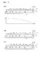
図2Aの上段は、第1のLEDアレイ101(参考例)を全体的に示す平面図である。なお、図中において、波長変換層80およびビア20dは破線によって示されている。 The upper part of FIG. 2A is a plan view generally showing the first LED array 101 (reference example). In the figure, the
LEDアレイ101は、たとえば、一方向に配列する6つのLED構造層を含み、それらLED構造層を覆うように波長変換層80が設けられている。6つのLED構造層を、図中において左側から順に、第1〜第6のLED構造層91a〜91fと呼ぶこととする。 The
6つのLED構造層91a〜91fは、電気的に直列に接続されており、たとえば直流電源装置に接続される。なお、各LED構造層は、交流(Duty)駆動方式で駆動してもよい。 The six LED structure layers 91a to 91f are electrically connected in series, and are connected to, for example, a DC power supply device. In addition, you may drive each LED structure layer by an alternating current (Duty) drive system.
LEDアレイ101を構成する第1〜第6のLED構造層91a〜91fは、それぞれ面積が異なっている。たとえば、第2のLED構造層91bの面積が、最も小さく、0.10mm2程度である。また、第1,3,4のLED構造層91a,91c、91dの面積がおよそ0.13mm2程度であり、第5のLED構造層91eの面積が0.21mm2程度である。そして、第6のLED構造層91fの面積が、最も大きく、0.37mm2程度である
LEDアレイ101では、各LED構造層に、同じサイズのビア20dが、行列状に一定の間隔で設けられている。全てのLED構造層において、ビア占有率は、およそ3.0%程度になっている。The first to sixth LED structure layers 91a to 91f constituting the
直列接続された第1〜第6のLED構造層91a〜91fに一定の電流を流したとき、各LED構造層の面積が異なるため、LED構造層各々で電流密度が異なり、さらには発光強度が異なる。この場合、LED構造層の面積と発光強度との間には負の相関関係が成立する。 When a constant current is passed through the first to sixth LED structure layers 91a to 91f connected in series, the area of each LED structure layer is different, so that the current density is different in each LED structure layer, and the emission intensity is further increased. Different. In this case, a negative correlation is established between the area of the LED structure layer and the light emission intensity.
図2Aの下段は、LEDアレイ101の光強度分布(輝度分布)特性を示すグラフである。グラフの横軸が、LEDアレイ101の延在方向(LED構造層の配列方向)の位置Xを示し、グラフの縦軸が、LEDアレイ101が出射する光の強度Iを示す。 The lower part of FIG. 2A is a graph showing the light intensity distribution (luminance distribution) characteristics of the
LEDアレイ101は、グラフに示すような山型ないし弓型の輝度分布特性を有する。つまり、LEDアレイ101の一端側(たとえば第1のLED構造層91a側)から他端側(たとえば第6のLED構造層91f側)にむかって、輝度が徐々に増加し、任意の位置で最大となり、そして、徐々に減少する特性を有する。 The
具体的には、第2のLED構造層91bの位置で輝度が最も高くなり、外側(両端側)に向かって徐々に輝度が低くなる特性を有する。各LED構造層の面積で言えば、第2のLED構造層91bの面積が最も小さく、外側(両端側)に向かって単調に面積が大きくなる傾向を有する。LEDアレイを車両用ヘッドライトに利用する場合、LEDアレイは、このような輝度分布特性を有していることが望ましい。 Specifically, the luminance is highest at the position of the second
一方で、LEDアレイを車両用ヘッドライトに利用する場合、LEDアレイの色ムラは抑制されている(色度分布は平坦化・均一化している)こと、つまり一様に白色に見えることが望ましい。本発明者らは、LEDアレイ101に100mA程度の電流を供給して、LEDアレイ101を発光させた際の色ムラ(色度分布)評価を行った。 On the other hand, when the LED array is used for a vehicle headlight, it is desirable that the color unevenness of the LED array is suppressed (the chromaticity distribution is flattened and uniform), that is, it looks uniform white. . The inventors of the present invention performed a color unevenness (chromaticity distribution) evaluation when the
その結果、LEDアレイ101において、面内の輝度が相対的に高い位置では、出射光の波長が短波長側(青色側)にシフトし、輝度が相対的に低い位置では、出射光の波長が長波長側(黄色側)にシフトすることがわかった。つまり、輝度が相対的に高い位置では、光半導体積層から放出される光がより強調されて出射光が青っぽい白色に見え、輝度が相対的に低い位置では、波長変換層で波長変換された光がより強調されて出射光が黄色っぽい白色に見えることがわかった。具体的には、輝度が最も高い第2のLED構造層91bが配置される位置で色度Cx(xy色度図におけるx成分)が概ね0.30程度となり、輝度が最も低い第6のLED構造層91fが配置される位置で色度Cxが概ね0.31程度になることがわかった。 As a result, in the
本発明者らの検討によれば、各LED構造層のビア占有率を変化させることにより、LEDアレイの色度分布特性を調整することができる。具体的には、ビア占有率を大きくすると、当該LED構造層の配置位置から出射する光の波長を相対的に長波長側にシフトさせることができ、逆に、ビア占有率を小さくすると、当該LED構造層の配置位置から出射する光の波長を相対的に短波長側にシフトさせることができる。これは、ビアが位置する部分は非発光領域であり、ビア直上の位置では蛍光体の色が強く出て、これが面全体の発光色にも影響するためである。たとえば、LEDアレイ101において、第2のLED構造層91bのビア占有率を3.0%から3.7%に大きくすると、第2のLED構造層91bが配置される位置の色度Cxが0.30から0.31に変化する。 According to the study by the present inventors, the chromaticity distribution characteristics of the LED array can be adjusted by changing the via occupation ratio of each LED structure layer. Specifically, when the via occupancy rate is increased, the wavelength of light emitted from the arrangement position of the LED structure layer can be relatively shifted to the longer wavelength side. The wavelength of the light emitted from the arrangement position of the LED structure layer can be relatively shifted to the short wavelength side. This is because the portion where the via is located is a non-light emitting region, and the phosphor color is strongly emitted at a position immediately above the via, which also affects the emission color of the entire surface. For example, in the
図2Bは、第2のLEDアレイ102(第1の実施例)を全体的に示す平面図である。第2のLEDアレイ102は、LED構造層各々のビア占有率を除いて、第1のLEDアレイ101と同様の構造を有する。6つのLED構造層を、図中において左側から順に、第1〜第6のLED構造層92a〜92fと呼ぶこととする。なお、各LED構造層のビア占有率は、単位面積当たりのビアの個数(密度)を変化させて調整してもよいし、一個当たりのビアのサイズ(直径)を変化させて調整してもよい。 FIG. 2B is a plan view generally showing the second LED array 102 (first embodiment). The
LEDアレイ102において、第1〜第6のLED構造層92a〜92fは、それぞれビア占有率が異なっている。具体的には、LED構造層の面積とビア占有率との間には負の相関関係が成立している。換言すれば、LED構造層の発光強度とビア占有率との間には正の相関関係が成立する。 In the
たとえば、第2のLED構造層92b(最大ビア占有率素子)のビア占有率が、最も大きく、4.3%程度である。また、第1,3,4のLED構造層92a,92c、92dのビア占有率がおよそ3.0%程度であり、第5のLED構造層92eのビア占有率が2.0%程度である。そして、第6のLED構造層92fのビア占有率が、最も小さく、1.2%程度である。 For example, the via occupation ratio of the second
LEDアレイ102において、輝度が最も高い第2のLED構造層92bのビア占有率が最も大きく、それ以外のLED構造層のビア占有率は、第2のLED構造層92bから離れるにしたがって、単調に減少していく傾向を有している。つまり、第2のLED構造層92bを除くLED構造層のビア占有率は、第2のLED構造層92bを中心として、そこから外側(両端側)に向かって、単調に減少していく傾向を有している。このように、輝度が高いLED構造層のビア占有率を相対的に高くし、輝度が低いLED構造層のビア占有率を相対的に低くすることにより、色ムラを抑制することができる(色度分布を平坦化・均一化することができる)。 In the
なお、第3,4のLED構造層92c、92dのように、隣接するLED構造層においてビア占有率が等しい箇所があってもかまわず、少なくても1か所は変化があることで全体として減少の傾向を示せればよい。ビアのサイズが変化する場合も、最もビアサイズが大きいLED構造層を中心としてそこから外側(両端側)に向かって単調に減少していく傾向を有しているが、一部では同じビアサイズのLED構造層を有していても、1か所は変化があることで全体として減少傾向を示せればよい。 It should be noted that there may be places where the via occupancy is equal in the adjacent LED structure layers, such as the third and fourth LED structure layers 92c and 92d, and at least one place is changed as a whole. What is necessary is just to show the decreasing tendency. Even when the via size changes, the LED structure layer having the largest via size has a tendency to monotonously decrease from the LED structure layer toward the outside (both ends). Even if it has a structural layer, it is only necessary to show a decreasing tendency as a whole because there is a change in one place.
また、上述したように、光半導体積層においてビアが形成されている領域は非発光領域となる。このため、各LED構造層のビア占有率が変化すると、LEDアレイの輝度分布特性も変化するものと考えられる。しかし、各LED構造層におけるビア占有率の変化が10%以下の範囲内で且つ数パーセント程度の変化であれば、LEDアレイの輝度分布特性はほとんど変化しないと考えられる。 Further, as described above, the region where the via is formed in the optical semiconductor stack is a non-light emitting region. For this reason, it is considered that when the via occupation ratio of each LED structure layer changes, the luminance distribution characteristic of the LED array also changes. However, if the change in via occupancy in each LED structure layer is within a range of 10% or less and a change of several percent, it is considered that the luminance distribution characteristics of the LED array hardly change.
図2Cは、第2のLEDアレイの変形例を示す平面図である。各LED構造層のビア占有率は、図2Bに示すように、単位面積当たりのビア20dの個数(密度)を変化させて調整してもよいし、図2Cに示すように、一個当たりのビア20dのサイズ(直径)を変化させて調整してもよい。 FIG. 2C is a plan view showing a modification of the second LED array. The via occupancy ratio of each LED structure layer may be adjusted by changing the number (density) of
図2Dは、第3のLEDアレイ103(第2の実施例)を全体的に示す平面図である。LEDアレイ103は、複数の、同じ平面形状を有するLED構造層93を含む。LED構造層93各々の平面形状は、たとえば正方形状である。 FIG. 2D is a plan view generally showing the third LED array 103 (second embodiment). The
複数のLED構造層93は、それぞれ電源装置に接続されており、それぞれ独立に電力を供給できるようになっている。個々のLED構造層93は、LEDアレイ103全体の輝度分布特性が、図2A下段のグラフに示される特性になるように、電力供給される。なお、LED構造層93各々の駆動方法は、直流駆動または交流(Duty)駆動のどちらでもよい。 The plurality of LED structure layers 93 are each connected to a power supply device, and can supply power independently. The individual LED structure layers 93 are supplied with power so that the luminance distribution characteristics of the
LEDアレイ103においても、輝度が最も高いLED構造層のビア占有率が最も大きく、それ以外のLED構造層のビア占有率は、輝度が最も高いLED構造層から離れるにしたがって、単調に減少していく傾向を有する。ここでは、左から2番目のLED構造層の輝度が最も高くなっているものとする。LED構造層に供給する電力を調整して所望の輝度分布特性を得る場合でも、高光出力のLED構造層におけるビア占有率を相対的に高くし、逆に、低光出力のLED構造層におけるビア占有率を相対的に低くすることにより、色ムラを抑制することができる。 Also in the
図2Eは、LEDアレイの駆動例を示す模式図である。図2A〜図2CのようにLED構造層のサイズが異なるように形成したLEDアレイに対しても個々のLED構造層ごとに駆動できるようにしてもよい。また、個々のLED構造層に駆動する方法としては、個々に電源を有する他、図2Eに示すようにスイッチ素子SWを設けることで電流を流すLED構造層を選択できるようにしてもよい。 FIG. 2E is a schematic diagram illustrating an example of driving the LED array. The LED array formed so that the size of the LED structure layer is different as shown in FIGS. 2A to 2C may be driven for each LED structure layer. Further, as a method of driving the individual LED structure layers, in addition to individually having a power supply, an LED structure layer that allows current to flow may be selected by providing a switch element SW as shown in FIG. 2E.
また、個々にLED構造層の駆動できる場合、電源装置の制御によってはその輝度分布を状況に応じて変化させることも可能となる。ただし、車両用灯具においては基本的な配向パターンというものはあらかじめ決められており、それに従いLEDアレイも形成される。よって、最適にはLEDアレイは基本的な配向パターンを再現する場合に輝度が最も高くなるLED構造層でビア占有率が最も高くなるよう設計される。結果として最もビア占有率の大きいLED構造層から離れるに従いビア占有率が減少していくLEDアレイが出来上がる。また、図2A〜図2CのようにLED構造層のサイズが異なる場合、最もLED構造層のサイズが小さいものが最も輝度を高くし易く、ビア占有率を最も高い素子とするのが好ましい。 Further, when the LED structure layer can be individually driven, the luminance distribution can be changed depending on the situation depending on the control of the power supply device. However, in the vehicular lamp, a basic orientation pattern is determined in advance, and an LED array is formed accordingly. Thus, optimally, the LED array is designed to have the highest via occupancy in the LED structure layer that has the highest luminance when reproducing the basic alignment pattern. As a result, an LED array in which the via occupancy decreases as the distance from the LED structure layer having the largest via occupancy increases. When the size of the LED structure layer is different as shown in FIGS. 2A to 2C, it is preferable that the element having the smallest LED structure layer has the highest luminance and has the highest via occupancy.
図2Fは、LEDアレイを用いた車両用灯具を示す模式図である。LEDアレイ101等の発光はレンズLを通して地面に照射される。LEDアレイは灯具のいずれに置かれるかは決められていない。ただし、地面に照射された場合、LED構造層91a,92aおよび図2Cにおける最も左のLED構造層が灯具から最も近い位置を照射し、LED構造層91f,92fおよび図2Cにおける最も右のLED構造層が灯具から最も遠い位置を照射する。 FIG. 2F is a schematic diagram illustrating a vehicular lamp using an LED array. Light emitted from the
図2Aの下段にあるように輝度のピークは配列方向の中心から一端に片寄った方向にある。同時にビア占有率が最も高いLED構造層は配列の一端に片寄った側に存在する。よって、図2Fの灯具は最大輝度ピークが片寄った方向(=ビア占有率が最も高いLED構造層が存在する側)が地面の近くを照射するよう配置され、反対側が地面の遠くを照射するように配置されている。 As shown in the lower part of FIG. 2A, the luminance peak is in a direction offset from the center in the arrangement direction to one end. At the same time, the LED structure layer with the highest via occupancy is on the side offset from one end of the array. Therefore, the lamp of FIG. 2F is arranged so that the direction in which the maximum luminance peak is offset (= the side where the LED structure layer having the highest via occupancy is present) irradiates near the ground, and the opposite side irradiates far from the ground. Is arranged.
尚、支持基板上に複数のLED構造層を形成する場合で説明したが、ビア電極構造の発光体が複数あればよく、基板上にフリップチップ型の素子を配列したものでも構わない。 In addition, although the case where a plurality of LED structure layers are formed on the support substrate has been described, a plurality of light emitters having a via electrode structure may be used, and a flip chip type element may be arranged on the substrate.
以上、実施例に沿って本発明を説明したが、本発明はこれらの実施例に限定されるものではない。たとえば、実施例では、支持基板上に、LED構造層が一列に配列する例を示したが、二列以上でLED構造層が配列していてもよい。その他、種々の変更、改良、組み合わせ等が可能なことは当業者には自明であろう。 As mentioned above, although this invention was demonstrated along the Example, this invention is not limited to these Examples. For example, in the embodiment, the example in which the LED structure layers are arranged in a row on the support substrate is shown, but the LED structure layers may be arranged in two or more rows. It will be apparent to those skilled in the art that other various modifications, improvements, combinations, and the like are possible.
11…成長基板、12…支持基板、20…光半導体積層、20d…ビア、21…バッファ層、22…n型半導体層、23…活性層(発光層)、24…p型半導体層、25…表面保護膜、30…p側電極、40…絶縁層、50…n側電極、60…第1接合層、61…第1接合層の第1導電領域、62…第1接合層の第2導電領域、70…第2接合層、71…第2接合層の第1導電領域、72…第2接合層の第2導電領域、73…第2接合層の第3導電領域、80…波長変換層、81…マトリクス部材、82…蛍光体材料、90,91,92,93…LED構造層、100,101,102,103…LEDアレイ。DESCRIPTION OF
Claims (8)
Translated fromJapanese前記基板の上方に、一方向に配列される複数の半導体発光素子と、
を備え、
前記半導体発光素子各々は、
前記基板側から、p型半導体層、発光性を有する活性層、n型半導体層が順次積層する光半導体積層、
前記基板側から、前記p型半導体層および前記活性層を貫通する、少なくとも1つ以上のビア、
前記ビアを通って、前記n型半導体層に接触するn側電極、および、
前記p型半導体層の表面に、前記ビアを避けるように設けられるp側電極、
を有し、
前記光半導体積層の面積に対する、前記ビアの総面積の比率をビア占有率と定義し、前記複数の半導体発光素子のうち、ビア占有率が最も大きい半導体発光素子を最大ビア占有率素子としたとき、
前記複数の半導体発光素子のうち、前記最大ビア占有率素子を除く半導体発光素子のビア占有率は、該最大ビア占有率素子から離れるにしたがって、単調に減少する傾向を有する、
半導体発光素子アレイ。A substrate,
A plurality of semiconductor light emitting elements arranged in one direction above the substrate;
With
Each of the semiconductor light emitting elements is
From the substrate side, a p-type semiconductor layer, a light-emitting active layer, an optical semiconductor stack in which an n-type semiconductor layer is sequentially stacked,
At least one or more vias penetrating the p-type semiconductor layer and the active layer from the substrate side;
An n-side electrode in contact with the n-type semiconductor layer through the via, and
A p-side electrode provided on the surface of the p-type semiconductor layer so as to avoid the via;
Have
When the ratio of the total area of the vias to the area of the optical semiconductor stack is defined as a via occupancy rate, a semiconductor light emitting device having the largest via occupancy rate among the plurality of semiconductor light emitting devices is defined as a maximum via occupancy rate element. ,
Among the plurality of semiconductor light emitting elements, the via occupation ratio of the semiconductor light emitting elements excluding the maximum via occupation ratio element has a tendency to monotonously decrease as the distance from the maximum via occupation ratio element increases.
Semiconductor light emitting element array.
前記複数の半導体発光素子のうち、前記最大ビア占有率素子の面積が最も小さく、該最大ビア占有率素子を除く半導体発光素子の面積は、該最大ビア占有率素子から離れるにしたがって、単調に増加する傾向を有する、
請求項1記載の半導体発光素子アレイ。Further, the semiconductor light emitting element is disposed between the support substrate and the plurality of semiconductor light emitting elements and connected to the n-side electrode and the p-side electrode of each of the plurality of semiconductor light emitting elements to electrically connect the plurality of semiconductor light emitting elements in series. A conductive layer connected to,
Of the plurality of semiconductor light emitting elements, the area of the maximum via occupancy element is the smallest, and the area of the semiconductor light emitting element excluding the maximum via occupancy element monotonously increases as the distance from the maximum via occupancy element increases. Have a tendency to
The semiconductor light-emitting element array according to claim 1.
前記電源装置により前記複数の半導体発光素子各々を駆動したとき、該複数の半導体発光素子のうち、前記最大ビア占有率素子の発光輝度が最も大きく、該最大ビア占有率素子を除く半導体発光素子の発光輝度は、該最大ビア占有率素子から離れるにしたがって、単調に減少する傾向を有する、
請求項1記載の半導体発光素子アレイ。And a power supply device connected to the n-side electrode and the p-side electrode of each of the plurality of semiconductor light emitting elements, and capable of independently driving the plurality of semiconductor light emitting elements,
When each of the plurality of semiconductor light emitting elements is driven by the power supply device, the light emission luminance of the maximum via occupancy element is the highest among the plurality of semiconductor light emitting elements, and the semiconductor light emitting element excluding the maximum via occupancy element The emission luminance has a tendency to monotonously decrease as the distance from the maximum via occupancy element increases.
The semiconductor light-emitting element array according to claim 1.
レンズと、を有し、
前記半導体発光素子アレイは前記最大ビア占有率素子が片寄った一端方向からの照射光が近傍を照射し、他端からの照射光が遠方を照射する車両用灯具。The semiconductor light emitting element array according to any one of claims 1 to 7, wherein the maximum via occupancy element is formed at a position offset to one end in an arrangement direction.
A lens, and
The semiconductor light emitting element array is a vehicular lamp in which the irradiation light from one end where the maximum via occupancy element is offset irradiates the vicinity, and the irradiation light from the other end irradiates far away.
Priority Applications (2)
| Application Number | Priority Date | Filing Date | Title |
|---|---|---|---|
| JP2015243987AJP6692155B2 (en) | 2015-12-15 | 2015-12-15 | Semiconductor light emitting element array and vehicle lamp |
| EP16203788.1AEP3182451B1 (en) | 2015-12-15 | 2016-12-13 | Light-emitting diode array and lighting device for vehicles |
Applications Claiming Priority (1)
| Application Number | Priority Date | Filing Date | Title |
|---|---|---|---|
| JP2015243987AJP6692155B2 (en) | 2015-12-15 | 2015-12-15 | Semiconductor light emitting element array and vehicle lamp |
Publications (2)
| Publication Number | Publication Date |
|---|---|
| JP2017112166Atrue JP2017112166A (en) | 2017-06-22 |
| JP6692155B2 JP6692155B2 (en) | 2020-05-13 |
Family
ID=57544355
Family Applications (1)
| Application Number | Title | Priority Date | Filing Date |
|---|---|---|---|
| JP2015243987AActiveJP6692155B2 (en) | 2015-12-15 | 2015-12-15 | Semiconductor light emitting element array and vehicle lamp |
Country Status (2)
| Country | Link |
|---|---|
| EP (1) | EP3182451B1 (en) |
| JP (1) | JP6692155B2 (en) |
Cited By (3)
| Publication number | Priority date | Publication date | Assignee | Title |
|---|---|---|---|---|
| JP2021535584A (en)* | 2018-10-11 | 2021-12-16 | 廈門市三安光電科技有限公司Xiamen San’An Optoelectronics Technology Co., Ltd. | Light emitting diode device and its manufacturing method |
| US11374151B2 (en) | 2019-07-23 | 2022-06-28 | Nichia Corporation | Light-emitting device |
| JP2023524892A (en)* | 2020-05-15 | 2023-06-13 | ルミレッズ リミテッド ライアビリティ カンパニー | A light-emitting device that can set the spatial distribution of radiant intensity |
Families Citing this family (5)
| Publication number | Priority date | Publication date | Assignee | Title |
|---|---|---|---|---|
| US11688710B2 (en) | 2019-03-25 | 2023-06-27 | Innolux Corporation | Electronic device |
| CN111739878B (en)* | 2019-03-25 | 2022-05-24 | 群创光电股份有限公司 | Electronic device |
| US11462666B2 (en) | 2020-05-15 | 2022-10-04 | Lumileds Llc | Light-emitting device with configurable spatial distribution of emission intensity |
| US11563148B2 (en) | 2020-05-15 | 2023-01-24 | Lumileds Llc | Light-emitting device with configurable spatial distribution of emission intensity |
| CN118633353B (en)* | 2021-12-01 | 2025-04-04 | 亮锐有限责任公司 | LED die with central peak surface brightness |
Citations (11)
| Publication number | Priority date | Publication date | Assignee | Title |
|---|---|---|---|---|
| JP2010103469A (en)* | 2008-10-22 | 2010-05-06 | Samsung Electro-Mechanics Co Ltd | Semiconductor light emitting device |
| JP2011066304A (en)* | 2009-09-18 | 2011-03-31 | Toyoda Gosei Co Ltd | Light-emitting element |
| JP2011513959A (en)* | 2008-02-29 | 2011-04-28 | オスラム オプト セミコンダクターズ ゲゼルシャフト ミット ベシュレンクテル ハフツング | Optoelectronic semiconductor body and manufacturing method thereof |
| JP2011517064A (en)* | 2008-03-31 | 2011-05-26 | オスラム オプト セミコンダクターズ ゲゼルシャフト ミット ベシュレンクテル ハフツング | Optoelectronic semiconductor chip and manufacturing method thereof |
| WO2013031210A1 (en)* | 2011-09-01 | 2013-03-07 | 株式会社小糸製作所 | Automotive headlamp apparatus |
| CN103500790A (en)* | 2013-10-08 | 2014-01-08 | 杭州士兰明芯科技有限公司 | Flip high-voltage light-emitting diode (LED) chip structure and manufacturing method thereof |
| US20140054631A1 (en)* | 2011-03-23 | 2014-02-27 | Epistar Corporation | Led array |
| WO2014192237A1 (en)* | 2013-05-30 | 2014-12-04 | スタンレー電気株式会社 | Semiconductor light-emitting element and semiconductor light-emitting device |
| JP2015501085A (en)* | 2011-12-22 | 2015-01-08 | オスラム オプト セミコンダクターズ ゲゼルシャフト ミット ベシュレンクテル ハフツングOsram Opto Semiconductors GmbH | Display device and manufacturing method of display device |
| DE102014103828A1 (en)* | 2014-03-20 | 2015-09-24 | Osram Opto Semiconductors Gmbh | Optoelectronic component and method for producing optoelectronic semiconductor components |
| JP2015177181A (en)* | 2014-03-18 | 2015-10-05 | スタンレー電気株式会社 | light-emitting device |
Family Cites Families (5)
| Publication number | Priority date | Publication date | Assignee | Title |
|---|---|---|---|---|
| US6828596B2 (en)* | 2002-06-13 | 2004-12-07 | Lumileds Lighting U.S., Llc | Contacting scheme for large and small area semiconductor light emitting flip chip devices |
| WO2010056083A2 (en)* | 2008-11-14 | 2010-05-20 | 삼성엘이디 주식회사 | Vertical/horizontal light-emitting diode for semiconductor |
| KR101252032B1 (en)* | 2010-07-08 | 2013-04-10 | 삼성전자주식회사 | Semiconductor light emitting device and method of manufacturing the same |
| JP5777879B2 (en) | 2010-12-27 | 2015-09-09 | ローム株式会社 | Light emitting device, light emitting device unit, and light emitting device package |
| KR20150117911A (en)* | 2014-04-11 | 2015-10-21 | 삼성전자주식회사 | Lighting device |
- 2015
- 2015-12-15JPJP2015243987Apatent/JP6692155B2/enactiveActive
- 2016
- 2016-12-13EPEP16203788.1Apatent/EP3182451B1/enactiveActive
Patent Citations (11)
| Publication number | Priority date | Publication date | Assignee | Title |
|---|---|---|---|---|
| JP2011513959A (en)* | 2008-02-29 | 2011-04-28 | オスラム オプト セミコンダクターズ ゲゼルシャフト ミット ベシュレンクテル ハフツング | Optoelectronic semiconductor body and manufacturing method thereof |
| JP2011517064A (en)* | 2008-03-31 | 2011-05-26 | オスラム オプト セミコンダクターズ ゲゼルシャフト ミット ベシュレンクテル ハフツング | Optoelectronic semiconductor chip and manufacturing method thereof |
| JP2010103469A (en)* | 2008-10-22 | 2010-05-06 | Samsung Electro-Mechanics Co Ltd | Semiconductor light emitting device |
| JP2011066304A (en)* | 2009-09-18 | 2011-03-31 | Toyoda Gosei Co Ltd | Light-emitting element |
| US20140054631A1 (en)* | 2011-03-23 | 2014-02-27 | Epistar Corporation | Led array |
| WO2013031210A1 (en)* | 2011-09-01 | 2013-03-07 | 株式会社小糸製作所 | Automotive headlamp apparatus |
| JP2015501085A (en)* | 2011-12-22 | 2015-01-08 | オスラム オプト セミコンダクターズ ゲゼルシャフト ミット ベシュレンクテル ハフツングOsram Opto Semiconductors GmbH | Display device and manufacturing method of display device |
| WO2014192237A1 (en)* | 2013-05-30 | 2014-12-04 | スタンレー電気株式会社 | Semiconductor light-emitting element and semiconductor light-emitting device |
| CN103500790A (en)* | 2013-10-08 | 2014-01-08 | 杭州士兰明芯科技有限公司 | Flip high-voltage light-emitting diode (LED) chip structure and manufacturing method thereof |
| JP2015177181A (en)* | 2014-03-18 | 2015-10-05 | スタンレー電気株式会社 | light-emitting device |
| DE102014103828A1 (en)* | 2014-03-20 | 2015-09-24 | Osram Opto Semiconductors Gmbh | Optoelectronic component and method for producing optoelectronic semiconductor components |
Cited By (7)
| Publication number | Priority date | Publication date | Assignee | Title |
|---|---|---|---|---|
| JP2021535584A (en)* | 2018-10-11 | 2021-12-16 | 廈門市三安光電科技有限公司Xiamen San’An Optoelectronics Technology Co., Ltd. | Light emitting diode device and its manufacturing method |
| JP7274511B2 (en) | 2018-10-11 | 2023-05-16 | 廈門市三安光電科技有限公司 | Light emitting diode device and manufacturing method thereof |
| JP2023100814A (en)* | 2018-10-11 | 2023-07-19 | 廈門市三安光電科技有限公司 | Light emitting diode device and manufacturing method thereof |
| JP7633305B2 (en) | 2018-10-11 | 2025-02-19 | 泉州三安半導体科技有限公司 | Light emitting diode device and method for fabricating same |
| US11374151B2 (en) | 2019-07-23 | 2022-06-28 | Nichia Corporation | Light-emitting device |
| JP2023524892A (en)* | 2020-05-15 | 2023-06-13 | ルミレッズ リミテッド ライアビリティ カンパニー | A light-emitting device that can set the spatial distribution of radiant intensity |
| JP7485790B2 (en) | 2020-05-15 | 2024-05-16 | ルミレッズ リミテッド ライアビリティ カンパニー | Light-emitting device capable of adjusting spatial distribution of radiation intensity |
Also Published As
| Publication number | Publication date |
|---|---|
| EP3182451B1 (en) | 2018-09-19 |
| JP6692155B2 (en) | 2020-05-13 |
| EP3182451A1 (en) | 2017-06-21 |
Similar Documents
| Publication | Publication Date | Title |
|---|---|---|
| JP6692155B2 (en) | Semiconductor light emitting element array and vehicle lamp | |
| US7880181B2 (en) | Light emitting diode with improved current spreading performance | |
| KR101630152B1 (en) | Hybrid light emitting diode chip and light emitting diode device having the same, and manufacturing method thereof | |
| JP6988460B2 (en) | Light emitting device, manufacturing method of light emitting device, and projector | |
| KR102018615B1 (en) | Semiconductor light emitting device and manufacturing method of the same | |
| KR20160008027A (en) | Semiconductor light emitting device and manufacturing method of the same | |
| JP6166954B2 (en) | Semiconductor light emitting element array and method for manufacturing semiconductor light emitting element array | |
| JP6537883B2 (en) | Semiconductor light emitting element and semiconductor light emitting element array | |
| KR101286210B1 (en) | Light emitting device and method fabricating the same | |
| CN111052409B (en) | Light emitting diode device and method of manufacturing light emitting diode device | |
| JP2012129281A (en) | Light-emitting device | |
| JP2015177023A (en) | Light emitting device | |
| JP6153351B2 (en) | Semiconductor light emitting device | |
| JP6106522B2 (en) | Semiconductor light emitting device array | |
| JP2017204593A (en) | Semiconductor light-emitting device | |
| JP2010251481A (en) | Light emitting device | |
| JP6265799B2 (en) | Semiconductor light emitting device | |
| JP2015056652A (en) | Nitride semiconductor light emitting device | |
| KR102175400B1 (en) | Semiconductor light emitting device with nano structure | |
| KR100670929B1 (en) | Light emitting device of flip chip structure and manufacturing method thereof | |
| KR100675268B1 (en) | A semiconductor light emitting device having a flip chip structure in which a plurality of light emitting cells are arranged and a method of manufacturing the same | |
| JP6262037B2 (en) | Light emitting device | |
| JP2010283124A (en) | Light emitting diode | |
| JP2012243972A (en) | Light emitting element | |
| KR20120031344A (en) | Light emitting diode chip and method for fabricating the same |
Legal Events
| Date | Code | Title | Description |
|---|---|---|---|
| A621 | Written request for application examination | Free format text:JAPANESE INTERMEDIATE CODE: A621 Effective date:20181114 | |
| A977 | Report on retrieval | Free format text:JAPANESE INTERMEDIATE CODE: A971007 Effective date:20190828 | |
| A131 | Notification of reasons for refusal | Free format text:JAPANESE INTERMEDIATE CODE: A131 Effective date:20190903 | |
| A521 | Request for written amendment filed | Free format text:JAPANESE INTERMEDIATE CODE: A523 Effective date:20191025 | |
| TRDD | Decision of grant or rejection written | ||
| A01 | Written decision to grant a patent or to grant a registration (utility model) | Free format text:JAPANESE INTERMEDIATE CODE: A01 Effective date:20200324 | |
| A61 | First payment of annual fees (during grant procedure) | Free format text:JAPANESE INTERMEDIATE CODE: A61 Effective date:20200414 | |
| R150 | Certificate of patent or registration of utility model | Ref document number:6692155 Country of ref document:JP Free format text:JAPANESE INTERMEDIATE CODE: R150 | |
| R250 | Receipt of annual fees | Free format text:JAPANESE INTERMEDIATE CODE: R250 | |
| R250 | Receipt of annual fees | Free format text:JAPANESE INTERMEDIATE CODE: R250 | |
| R250 | Receipt of annual fees | Free format text:JAPANESE INTERMEDIATE CODE: R250 |