JP2017092314A - Method for separating SiC substrate - Google Patents
Method for separating SiC substrateDownload PDFInfo
- Publication number
- JP2017092314A JP2017092314AJP2015222369AJP2015222369AJP2017092314AJP 2017092314 AJP2017092314 AJP 2017092314AJP 2015222369 AJP2015222369 AJP 2015222369AJP 2015222369 AJP2015222369 AJP 2015222369AJP 2017092314 AJP2017092314 AJP 2017092314A
- Authority
- JP
- Japan
- Prior art keywords
- sic substrate
- adhesive tape
- separation
- laser beam
- separating
- Prior art date
- Legal status (The legal status is an assumption and is not a legal conclusion. Google has not performed a legal analysis and makes no representation as to the accuracy of the status listed.)
- Granted
Links
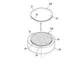
Images


Classifications
- B—PERFORMING OPERATIONS; TRANSPORTING
- B23—MACHINE TOOLS; METAL-WORKING NOT OTHERWISE PROVIDED FOR
- B23K—SOLDERING OR UNSOLDERING; WELDING; CLADDING OR PLATING BY SOLDERING OR WELDING; CUTTING BY APPLYING HEAT LOCALLY, e.g. FLAME CUTTING; WORKING BY LASER BEAM
- B23K26/00—Working by laser beam, e.g. welding, cutting or boring
- B23K26/36—Removing material
- B23K26/38—Removing material by boring or cutting
- H—ELECTRICITY
- H01—ELECTRIC ELEMENTS
- H01L—SEMICONDUCTOR DEVICES NOT COVERED BY CLASS H10
- H01L21/00—Processes or apparatus adapted for the manufacture or treatment of semiconductor or solid state devices or of parts thereof
- H01L21/70—Manufacture or treatment of devices consisting of a plurality of solid state components formed in or on a common substrate or of parts thereof; Manufacture of integrated circuit devices or of parts thereof
- H01L21/77—Manufacture or treatment of devices consisting of a plurality of solid state components or integrated circuits formed in, or on, a common substrate
- H01L21/78—Manufacture or treatment of devices consisting of a plurality of solid state components or integrated circuits formed in, or on, a common substrate with subsequent division of the substrate into plural individual devices
- H01L21/7806—Manufacture or treatment of devices consisting of a plurality of solid state components or integrated circuits formed in, or on, a common substrate with subsequent division of the substrate into plural individual devices involving the separation of the active layers from a substrate
- B—PERFORMING OPERATIONS; TRANSPORTING
- B23—MACHINE TOOLS; METAL-WORKING NOT OTHERWISE PROVIDED FOR
- B23K—SOLDERING OR UNSOLDERING; WELDING; CLADDING OR PLATING BY SOLDERING OR WELDING; CUTTING BY APPLYING HEAT LOCALLY, e.g. FLAME CUTTING; WORKING BY LASER BEAM
- B23K26/00—Working by laser beam, e.g. welding, cutting or boring
- B23K26/50—Working by transmitting the laser beam through or within the workpiece
- B23K26/53—Working by transmitting the laser beam through or within the workpiece for modifying or reforming the material inside the workpiece, e.g. for producing break initiation cracks
- B—PERFORMING OPERATIONS; TRANSPORTING
- B23—MACHINE TOOLS; METAL-WORKING NOT OTHERWISE PROVIDED FOR
- B23K—SOLDERING OR UNSOLDERING; WELDING; CLADDING OR PLATING BY SOLDERING OR WELDING; CUTTING BY APPLYING HEAT LOCALLY, e.g. FLAME CUTTING; WORKING BY LASER BEAM
- B23K26/00—Working by laser beam, e.g. welding, cutting or boring
- B23K26/0006—Working by laser beam, e.g. welding, cutting or boring taking account of the properties of the material involved
- B—PERFORMING OPERATIONS; TRANSPORTING
- B23—MACHINE TOOLS; METAL-WORKING NOT OTHERWISE PROVIDED FOR
- B23K—SOLDERING OR UNSOLDERING; WELDING; CLADDING OR PLATING BY SOLDERING OR WELDING; CUTTING BY APPLYING HEAT LOCALLY, e.g. FLAME CUTTING; WORKING BY LASER BEAM
- B23K26/00—Working by laser beam, e.g. welding, cutting or boring
- B23K26/02—Positioning or observing the workpiece, e.g. with respect to the point of impact; Aligning, aiming or focusing the laser beam
- B23K26/03—Observing, e.g. monitoring, the workpiece
- B23K26/032—Observing, e.g. monitoring, the workpiece using optical means
- B—PERFORMING OPERATIONS; TRANSPORTING
- B23—MACHINE TOOLS; METAL-WORKING NOT OTHERWISE PROVIDED FOR
- B23K—SOLDERING OR UNSOLDERING; WELDING; CLADDING OR PLATING BY SOLDERING OR WELDING; CUTTING BY APPLYING HEAT LOCALLY, e.g. FLAME CUTTING; WORKING BY LASER BEAM
- B23K26/00—Working by laser beam, e.g. welding, cutting or boring
- B23K26/02—Positioning or observing the workpiece, e.g. with respect to the point of impact; Aligning, aiming or focusing the laser beam
- B23K26/06—Shaping the laser beam, e.g. by masks or multi-focusing
- B23K26/062—Shaping the laser beam, e.g. by masks or multi-focusing by direct control of the laser beam
- B23K26/0622—Shaping the laser beam, e.g. by masks or multi-focusing by direct control of the laser beam by shaping pulses
- B—PERFORMING OPERATIONS; TRANSPORTING
- B23—MACHINE TOOLS; METAL-WORKING NOT OTHERWISE PROVIDED FOR
- B23K—SOLDERING OR UNSOLDERING; WELDING; CLADDING OR PLATING BY SOLDERING OR WELDING; CUTTING BY APPLYING HEAT LOCALLY, e.g. FLAME CUTTING; WORKING BY LASER BEAM
- B23K26/00—Working by laser beam, e.g. welding, cutting or boring
- B23K26/08—Devices involving relative movement between laser beam and workpiece
- B23K26/082—Scanning systems, i.e. devices involving movement of the laser beam relative to the laser head
- B—PERFORMING OPERATIONS; TRANSPORTING
- B23—MACHINE TOOLS; METAL-WORKING NOT OTHERWISE PROVIDED FOR
- B23K—SOLDERING OR UNSOLDERING; WELDING; CLADDING OR PLATING BY SOLDERING OR WELDING; CUTTING BY APPLYING HEAT LOCALLY, e.g. FLAME CUTTING; WORKING BY LASER BEAM
- B23K26/00—Working by laser beam, e.g. welding, cutting or boring
- B23K26/08—Devices involving relative movement between laser beam and workpiece
- B23K26/0823—Devices involving rotation of the workpiece
- B—PERFORMING OPERATIONS; TRANSPORTING
- B23—MACHINE TOOLS; METAL-WORKING NOT OTHERWISE PROVIDED FOR
- B23K—SOLDERING OR UNSOLDERING; WELDING; CLADDING OR PLATING BY SOLDERING OR WELDING; CUTTING BY APPLYING HEAT LOCALLY, e.g. FLAME CUTTING; WORKING BY LASER BEAM
- B23K26/00—Working by laser beam, e.g. welding, cutting or boring
- B23K26/08—Devices involving relative movement between laser beam and workpiece
- B23K26/083—Devices involving movement of the workpiece in at least one axial direction
- B23K26/0853—Devices involving movement of the workpiece in at least in two axial directions, e.g. in a plane
- B—PERFORMING OPERATIONS; TRANSPORTING
- B23—MACHINE TOOLS; METAL-WORKING NOT OTHERWISE PROVIDED FOR
- B23K—SOLDERING OR UNSOLDERING; WELDING; CLADDING OR PLATING BY SOLDERING OR WELDING; CUTTING BY APPLYING HEAT LOCALLY, e.g. FLAME CUTTING; WORKING BY LASER BEAM
- B23K26/00—Working by laser beam, e.g. welding, cutting or boring
- B23K26/08—Devices involving relative movement between laser beam and workpiece
- B23K26/0869—Devices involving movement of the laser head in at least one axial direction
- B23K26/0876—Devices involving movement of the laser head in at least one axial direction in at least two axial directions
- B—PERFORMING OPERATIONS; TRANSPORTING
- B24—GRINDING; POLISHING
- B24B—MACHINES, DEVICES, OR PROCESSES FOR GRINDING OR POLISHING; DRESSING OR CONDITIONING OF ABRADING SURFACES; FEEDING OF GRINDING, POLISHING, OR LAPPING AGENTS
- B24B9/00—Machines or devices designed for grinding edges or bevels on work or for removing burrs; Accessories therefor
- B24B9/02—Machines or devices designed for grinding edges or bevels on work or for removing burrs; Accessories therefor characterised by a special design with respect to properties of materials specific to articles to be ground
- B24B9/06—Machines or devices designed for grinding edges or bevels on work or for removing burrs; Accessories therefor characterised by a special design with respect to properties of materials specific to articles to be ground of non-metallic inorganic material, e.g. stone, ceramics, porcelain
- B24B9/065—Machines or devices designed for grinding edges or bevels on work or for removing burrs; Accessories therefor characterised by a special design with respect to properties of materials specific to articles to be ground of non-metallic inorganic material, e.g. stone, ceramics, porcelain of thin, brittle parts, e.g. semiconductors, wafers
- B—PERFORMING OPERATIONS; TRANSPORTING
- B28—WORKING CEMENT, CLAY, OR STONE
- B28D—WORKING STONE OR STONE-LIKE MATERIALS
- B28D5/00—Fine working of gems, jewels, crystals, e.g. of semiconductor material; apparatus or devices therefor
- H—ELECTRICITY
- H01—ELECTRIC ELEMENTS
- H01L—SEMICONDUCTOR DEVICES NOT COVERED BY CLASS H10
- H01L21/00—Processes or apparatus adapted for the manufacture or treatment of semiconductor or solid state devices or of parts thereof
- H01L21/02—Manufacture or treatment of semiconductor devices or of parts thereof
- H01L21/02002—Preparing wafers
- H01L21/02005—Preparing bulk and homogeneous wafers
- H01L21/02008—Multistep processes
- H01L21/0201—Specific process step
- H01L21/02013—Grinding, lapping
- H—ELECTRICITY
- H01—ELECTRIC ELEMENTS
- H01L—SEMICONDUCTOR DEVICES NOT COVERED BY CLASS H10
- H01L21/00—Processes or apparatus adapted for the manufacture or treatment of semiconductor or solid state devices or of parts thereof
- H01L21/02—Manufacture or treatment of semiconductor devices or of parts thereof
- H01L21/02104—Forming layers
- H01L21/02365—Forming inorganic semiconducting materials on a substrate
- H01L21/02367—Substrates
- H01L21/0237—Materials
- H01L21/02373—Group 14 semiconducting materials
- H01L21/02378—Silicon carbide
- H—ELECTRICITY
- H01—ELECTRIC ELEMENTS
- H01L—SEMICONDUCTOR DEVICES NOT COVERED BY CLASS H10
- H01L21/00—Processes or apparatus adapted for the manufacture or treatment of semiconductor or solid state devices or of parts thereof
- H01L21/02—Manufacture or treatment of semiconductor devices or of parts thereof
- H01L21/04—Manufacture or treatment of semiconductor devices or of parts thereof the devices having potential barriers, e.g. a PN junction, depletion layer or carrier concentration layer
- H01L21/18—Manufacture or treatment of semiconductor devices or of parts thereof the devices having potential barriers, e.g. a PN junction, depletion layer or carrier concentration layer the devices having semiconductor bodies comprising elements of Group IV of the Periodic Table or AIIIBV compounds with or without impurities, e.g. doping materials
- H01L21/26—Bombardment with radiation
- H01L21/263—Bombardment with radiation with high-energy radiation
- H01L21/268—Bombardment with radiation with high-energy radiation using electromagnetic radiation, e.g. laser radiation
- H—ELECTRICITY
- H01—ELECTRIC ELEMENTS
- H01L—SEMICONDUCTOR DEVICES NOT COVERED BY CLASS H10
- H01L21/00—Processes or apparatus adapted for the manufacture or treatment of semiconductor or solid state devices or of parts thereof
- H01L21/67—Apparatus specially adapted for handling semiconductor or electric solid state devices during manufacture or treatment thereof; Apparatus specially adapted for handling wafers during manufacture or treatment of semiconductor or electric solid state devices or components ; Apparatus not specifically provided for elsewhere
- H01L21/683—Apparatus specially adapted for handling semiconductor or electric solid state devices during manufacture or treatment thereof; Apparatus specially adapted for handling wafers during manufacture or treatment of semiconductor or electric solid state devices or components ; Apparatus not specifically provided for elsewhere for supporting or gripping
- H01L21/6835—Apparatus specially adapted for handling semiconductor or electric solid state devices during manufacture or treatment thereof; Apparatus specially adapted for handling wafers during manufacture or treatment of semiconductor or electric solid state devices or components ; Apparatus not specifically provided for elsewhere for supporting or gripping using temporarily an auxiliary support
- H01L21/6836—Wafer tapes, e.g. grinding or dicing support tapes
- H—ELECTRICITY
- H01—ELECTRIC ELEMENTS
- H01L—SEMICONDUCTOR DEVICES NOT COVERED BY CLASS H10
- H01L21/00—Processes or apparatus adapted for the manufacture or treatment of semiconductor or solid state devices or of parts thereof
- H01L21/70—Manufacture or treatment of devices consisting of a plurality of solid state components formed in or on a common substrate or of parts thereof; Manufacture of integrated circuit devices or of parts thereof
- H01L21/71—Manufacture of specific parts of devices defined in group H01L21/70
- H01L21/76—Making of isolation regions between components
- H—ELECTRICITY
- H01—ELECTRIC ELEMENTS
- H01L—SEMICONDUCTOR DEVICES NOT COVERED BY CLASS H10
- H01L21/00—Processes or apparatus adapted for the manufacture or treatment of semiconductor or solid state devices or of parts thereof
- H01L21/70—Manufacture or treatment of devices consisting of a plurality of solid state components formed in or on a common substrate or of parts thereof; Manufacture of integrated circuit devices or of parts thereof
- H01L21/77—Manufacture or treatment of devices consisting of a plurality of solid state components or integrated circuits formed in, or on, a common substrate
- H01L21/78—Manufacture or treatment of devices consisting of a plurality of solid state components or integrated circuits formed in, or on, a common substrate with subsequent division of the substrate into plural individual devices
- B—PERFORMING OPERATIONS; TRANSPORTING
- B23—MACHINE TOOLS; METAL-WORKING NOT OTHERWISE PROVIDED FOR
- B23K—SOLDERING OR UNSOLDERING; WELDING; CLADDING OR PLATING BY SOLDERING OR WELDING; CUTTING BY APPLYING HEAT LOCALLY, e.g. FLAME CUTTING; WORKING BY LASER BEAM
- B23K2103/00—Materials to be soldered, welded or cut
- B23K2103/50—Inorganic material, e.g. metals, not provided for in B23K2103/02 – B23K2103/26
- B23K2103/56—Inorganic material, e.g. metals, not provided for in B23K2103/02 – B23K2103/26 semiconducting
- H—ELECTRICITY
- H01—ELECTRIC ELEMENTS
- H01L—SEMICONDUCTOR DEVICES NOT COVERED BY CLASS H10
- H01L2221/00—Processes or apparatus adapted for the manufacture or treatment of semiconductor or solid state devices or of parts thereof covered by H01L21/00
- H01L2221/67—Apparatus for handling semiconductor or electric solid state devices during manufacture or treatment thereof; Apparatus for handling wafers during manufacture or treatment of semiconductor or electric solid state devices or components; Apparatus not specifically provided for elsewhere
- H01L2221/683—Apparatus for handling semiconductor or electric solid state devices during manufacture or treatment thereof; Apparatus for handling wafers during manufacture or treatment of semiconductor or electric solid state devices or components; Apparatus not specifically provided for elsewhere for supporting or gripping
- H01L2221/68304—Apparatus for handling semiconductor or electric solid state devices during manufacture or treatment thereof; Apparatus for handling wafers during manufacture or treatment of semiconductor or electric solid state devices or components; Apparatus not specifically provided for elsewhere for supporting or gripping using temporarily an auxiliary support
- H01L2221/68327—Apparatus for handling semiconductor or electric solid state devices during manufacture or treatment thereof; Apparatus for handling wafers during manufacture or treatment of semiconductor or electric solid state devices or components; Apparatus not specifically provided for elsewhere for supporting or gripping using temporarily an auxiliary support used during dicing or grinding
- H—ELECTRICITY
- H10—SEMICONDUCTOR DEVICES; ELECTRIC SOLID-STATE DEVICES NOT OTHERWISE PROVIDED FOR
- H10D—INORGANIC ELECTRIC SEMICONDUCTOR DEVICES
- H10D62/00—Semiconductor bodies, or regions thereof, of devices having potential barriers
- H10D62/80—Semiconductor bodies, or regions thereof, of devices having potential barriers characterised by the materials
- H10D62/83—Semiconductor bodies, or regions thereof, of devices having potential barriers characterised by the materials being Group IV materials, e.g. B-doped Si or undoped Ge
- H10D62/832—Semiconductor bodies, or regions thereof, of devices having potential barriers characterised by the materials being Group IV materials, e.g. B-doped Si or undoped Ge being Group IV materials comprising two or more elements, e.g. SiGe
- H10D62/8325—Silicon carbide
Landscapes
- Engineering & Computer Science (AREA)
- Physics & Mathematics (AREA)
- Optics & Photonics (AREA)
- Mechanical Engineering (AREA)
- Plasma & Fusion (AREA)
- Microelectronics & Electronic Packaging (AREA)
- Condensed Matter Physics & Semiconductors (AREA)
- Power Engineering (AREA)
- Computer Hardware Design (AREA)
- Manufacturing & Machinery (AREA)
- General Physics & Mathematics (AREA)
- Chemical & Material Sciences (AREA)
- High Energy & Nuclear Physics (AREA)
- Oil, Petroleum & Natural Gas (AREA)
- Inorganic Chemistry (AREA)
- Chemical Kinetics & Catalysis (AREA)
- General Chemical & Material Sciences (AREA)
- Ceramic Engineering (AREA)
- Electromagnetism (AREA)
- Health & Medical Sciences (AREA)
- Toxicology (AREA)
- Materials Engineering (AREA)
- Mechanical Treatment Of Semiconductor (AREA)
- Laser Beam Processing (AREA)
- Processing Of Stones Or Stones Resemblance Materials (AREA)
- Crystals, And After-Treatments Of Crystals (AREA)
Abstract
Description
Translated fromJapanese本発明は、SiC基板を少なくとも2枚に分離するSiC基板の分離方法に関する。 The present invention relates to an SiC substrate separation method for separating an SiC substrate into at least two sheets.
IC、LSI等の各種デバイスは、シリコン等を素材としたウエーハの表面に機能層を積層し、この機能層に複数の分割予定ラインによって区画された領域に形成される。そして、切削装置、レーザー加工装置等の加工装置によってウエーハの分割予定ラインに加工が施され、ウエーハが個々のデバイスチップに分割され、分割されたデバイスチップは携帯電話、パソコン等の各種電子機器に広く利用されている。 Various devices such as IC and LSI are formed in a region partitioned by a plurality of scheduled division lines on a functional layer laminated on the surface of a wafer made of silicon or the like. Then, the wafer division line is processed by a processing device such as a cutting device or a laser processing device, the wafer is divided into individual device chips, and the divided device chips are applied to various electronic devices such as mobile phones and personal computers. Widely used.
また、パワーデバイス又はLED、LD等の光デバイスは、SiC、GaN等の六方晶単結晶を素材としたウエーハの表面に機能層が積層され、積層された機能層に格子状に形成された複数の分割予定ラインによって区画されて形成される。 In addition, a power device or an optical device such as an LED or LD has a functional layer laminated on the surface of a wafer made of a hexagonal single crystal such as SiC or GaN, and a plurality of layers formed in a lattice shape on the laminated functional layer. It is divided and formed by a predetermined dividing line.
デバイスが形成されるウエーハは、一般的にインゴットをワイヤーソーでスライスして生成され、スライスされたウエーハの表裏面を研磨して鏡面に仕上げられる(例えば、特開2000−94221号公報参照)。 The wafer on which the device is formed is generally produced by slicing an ingot with a wire saw, and the front and back surfaces of the sliced wafer are polished to a mirror finish (see, for example, Japanese Patent Application Laid-Open No. 2000-94221).
このワイヤーソーでは、直径約100〜300μmのピアノ線等の一本のワイヤーを通常二〜四本の間隔補助ローラー上に設けられた多数の溝に巻き付けて、一定ピッチで互いに平行に配置してワイヤーを一定方向又は双方向に走行させて、インゴットを複数のウエーハにスライスする。 In this wire saw, a single wire such as a piano wire having a diameter of about 100 to 300 μm is usually wound around a number of grooves provided on two to four spacing auxiliary rollers and arranged parallel to each other at a constant pitch. An ingot is sliced into a plurality of wafers by running the wire in a certain direction or in both directions.
しかし、インゴットをワイヤーソーで切断し、表裏面を研磨してウエーハを生成すると、インゴットの70〜80%が捨てられることになり、不経済であるという問題がある。特に、SiC、GaN等の六方晶単結晶インゴットはモース硬度が高く、ワイヤーソーでの切断が困難であり相当な時間がかかり生産性が悪く、効率よくウエーハを生成することに課題を有している。 However, when the ingot is cut with a wire saw and the front and back surfaces are polished to produce a wafer, 70 to 80% of the ingot is discarded, which is uneconomical. In particular, hexagonal single crystal ingots such as SiC and GaN have high Mohs hardness, are difficult to cut with a wire saw, take a considerable amount of time, have poor productivity, and have a problem in efficiently producing a wafer. Yes.
これらの問題を解決するために、SiCに対して透過性を有する波長のレーザービームの集光点をSiC基板又はSiCインゴットの内部に位置づけて照射し、切断予定面に改質層及びクラックを形成し、外力を付与してウエーハを改質層及びクラックが形成された切断予定面に沿って割断して、SiC基板からウエーハを分離する技術が特開2013−49461号公報に記載されている。 In order to solve these problems, a condensing point of a laser beam having a wavelength that is permeable to SiC is positioned inside the SiC substrate or SiC ingot, and a modified layer and a crack are formed on the planned cutting surface. Japanese Laid-Open Patent Publication No. 2013-49461 discloses a technique for separating an wafer from an SiC substrate by applying an external force to cleave the wafer along a planned cutting surface where a modified layer and a crack are formed.
この公開公報に記載された技術では、パルスレーザービームの第1の照射点と該第1の照射点に最も近い第2の照射点とが所定位置となるように、パルスレーザービームの集光点を切断予定面に沿って螺旋状に照射するか、又は直線状に照射して、非常に高密度な改質層及びクラックをSiC基板の切断予定面に形成している。 In the technique described in this publication, the condensing point of the pulse laser beam is set so that the first irradiation point of the pulse laser beam and the second irradiation point closest to the first irradiation point are in a predetermined position. Is irradiated spirally along the planned cutting surface, or is irradiated linearly to form a very high density modified layer and cracks on the planned cutting surface of the SiC substrate.
しかし、特許文献2記載のSiC基板又はSiCインゴットの切断方法では、レーザービームの照射方法は基板又はインゴットに対して螺旋状又は直線状であり、直線状の場合レーザービームを走査する方向は何ら規定されていない。 However, in the method of cutting an SiC substrate or SiC ingot described in Patent Document 2, the laser beam irradiation method is spiral or linear with respect to the substrate or ingot, and in the case of a linear shape, the direction in which the laser beam is scanned is defined in any way. It has not been.
特許文献2に記載されたSiC基板又はSiCインゴットの切断方法では、レーザービームの第1の照射点と該第1の照射点に最も近い第2の照射点との間のピッチを1μm〜10μmに設定している。このピッチは、改質層から生じた割れがc面に沿って伸びるピッチである。 In the SiC substrate or SiC ingot cutting method described in Patent Document 2, the pitch between the first irradiation point of the laser beam and the second irradiation point closest to the first irradiation point is set to 1 μm to 10 μm. It is set. This pitch is a pitch at which cracks generated from the modified layer extend along the c-plane.
このようにレーザービームを照射する際のピッチが非常に小さいため、レーザービームの照射方法が螺旋状であっても又は直線状であっても、非常に小さなピッチ間隔でレーザービームを照射する必要があり、生産性の向上が十分図られていないという問題がある。 Since the pitch when irradiating the laser beam is very small in this way, it is necessary to irradiate the laser beam at a very small pitch interval, regardless of whether the laser beam irradiation method is spiral or linear. There is a problem that productivity is not sufficiently improved.
更に、SiC基板の内部に形成された改質層及びクラックからなる分離起点からウエーハを分離する際、ウエーハが比較的薄いためウエーハが破損するという問題がある。 Furthermore, when the wafer is separated from the separation starting point composed of the modified layer and cracks formed inside the SiC substrate, there is a problem that the wafer is damaged because the wafer is relatively thin.
本発明はこのような点に鑑みてなされたものであり、その目的とするところは、SiC基板を破損することなく少なくとも2枚に分離できるSiC基板の分離方法を提供することである。 This invention is made | formed in view of such a point, The place made into the objective is providing the separation method of the SiC substrate which can be separated into at least 2 piece without damaging a SiC substrate.
請求項1記載の発明によると、第1の面と該第1の面と反対側の第2の面とを有するSiC基板を少なくとも2枚に分離するSiC基板の分離方法であって、該第1の面に透明な粘着テープを貼着する粘着テープ貼着ステップと、該第2の面に保持部材を貼着する保持部材貼着ステップと、該粘着テープ貼着ステップ及び該保持部材貼着ステップを実施した後、SiC基板及び該粘着テープに対して透過性を有する波長のレーザービームの集光点を該粘着テープ側からSiC基板の内部に位置付けると共に、該集光点とSiC基板とを相対的に移動しながらレーザービームを該粘着テープに照射し、該第1の面に平行な改質層及びクラックとを形成して分離起点とする分離起点形成ステップと、該分離起点形成ステップを実施した後、外力を付与して該分離起点から該粘着テープと共に該第1の面を有するSiC基板を該第2の面を有するSiC基板から分離する分離ステップと、を備えたことを特徴とするSiC基板の分離方法が提供される。 According to the first aspect of the present invention, there is provided a SiC substrate separation method for separating an SiC substrate having a first surface and a second surface opposite to the first surface into at least two sheets. An adhesive tape adhering step for adhering a transparent adhesive tape to one surface, a holding member adhering step for adhering a holding member to the second surface, the adhesive tape adhering step, and the holding member adhering After performing the step, the condensing point of the laser beam having a wavelength transmissive to the SiC substrate and the adhesive tape is positioned inside the SiC substrate from the adhesive tape side, and the condensing point and the SiC substrate are A separation starting point forming step in which a laser beam is irradiated onto the adhesive tape while moving relatively to form a modified layer and a crack parallel to the first surface to form a separation starting point, and the separation starting point forming step. After carrying out the external force Separating the SiC substrate having the first surface together with the adhesive tape from the separation starting point, and separating the SiC substrate having the second surface. Is provided.
好ましくは、SiC基板の分離方法は、第1の面を有するSiC基板の分離起点となった面及び第2の面を有するSiC基板の分離起点となった面を研削砥石によって研削して平坦化する平坦化ステップを更に備えている。 Preferably, in the SiC substrate separation method, the surface that is the separation starting point of the SiC substrate having the first surface and the surface that is the separation starting point of the SiC substrate having the second surface are ground and ground by a grinding wheel. And a planarizing step.
請求項4記載の発明によると、第1の面と、該第1の面と反対側の第2の面と、該第1の面から該第2の面に至るc軸と、該c軸に直交するc面とを有するSiC基板を少なくとも2枚に分離するSiC基板の分離方法であって、該第1の面に透明な粘着テープを貼着する粘着テープ貼着ステップと、該第2の面に保持部材を貼着する保持部材貼着ステップと、該粘着テープ貼着ステップ及び該保持部材貼着ステップを実施した後、SiC基板及び該粘着テープに対して透過性を有する波長のレーザービームの集光点を該粘着テープ側からSiC基板の内部に位置付けると共に、該集光点とSiC基板とを相対的に移動しながらレーザービームを該粘着テープに照射し、該第1の面に平行な改質層及びクラックとを形成して分離起点とする分離起点形成ステップと、該分離起点形成ステップを実施した後、外力を付与して該分離起点から該粘着テープと共に該第1の面を有するSiC基板を該第2の面を有するSiC基板から分離する分離ステップと、を備え、該分離起点形成ステップは、該第1の面の垂線に対して該c軸がオフ角分傾き、該第1の面と該c面との間にオフ角が形成される方向と直交する方向にレーザービームの集光点を相対的に移動して直線状の改質層を形成する改質層形成ステップと、該オフ角が形成される方向に該集光点を相対的に移動して所定量インデックスするインデックスステップと、を含むことを特徴とするSiC基板の分離方法が提供される。 According to a fourth aspect of the present invention, the first surface, the second surface opposite to the first surface, the c-axis extending from the first surface to the second surface, and the c-axis An SiC substrate separation method for separating an SiC substrate having a c-plane orthogonal to at least two sheets, an adhesive tape attaching step of attaching a transparent adhesive tape to the first surface, and the second After carrying out the holding member sticking step for sticking the holding member on the surface, the adhesive tape sticking step and the holding member sticking step, a laser having a wavelength having transparency to the SiC substrate and the adhesive tape The focusing point of the beam is positioned inside the SiC substrate from the adhesive tape side, and the adhesive tape is irradiated with a laser beam while moving the focusing point and the SiC substrate relatively to the first surface. The separation starting point by forming parallel modified layers and cracks After performing the starting point forming step and the separation starting point forming step, an external force is applied to separate the SiC substrate having the first surface together with the adhesive tape from the SiC substrate having the second surface from the separation starting point. A separation step, wherein the c-axis is inclined by an off-angle with respect to the normal of the first surface, and an off-angle is formed between the first surface and the c-plane. A modified layer forming step of forming a linear modified layer by relatively moving the focal point of the laser beam in a direction perpendicular to the direction in which the laser beam is focused, and the focal point in the direction in which the off angle is formed And an indexing step for indexing a predetermined amount by relatively moving the substrate, a method for separating a SiC substrate is provided.
請求項1記載のSiC基板の分離方法によると、SiC基板の第1の面が粘着テープによって補強されているため、第1の面を有するSiC基板を第2の面を有するSiC基板から破損することなく分離することができる。 According to the method for separating a SiC substrate according to claim 1, since the first surface of the SiC substrate is reinforced by the adhesive tape, the SiC substrate having the first surface is broken from the SiC substrate having the second surface. Can be separated without any problems.
また、SiC基板の第1の面に貼着された粘着テープの屈折率は空気より大きくSiC基板より小さいので、粘着テープを介したことによりレーザービームの反射が抑制され、SiC基板の内部にレーザービームを効率よく導くことができる。 In addition, since the refractive index of the adhesive tape attached to the first surface of the SiC substrate is larger than air and smaller than that of the SiC substrate, the reflection of the laser beam is suppressed by passing through the adhesive tape, and the laser is reflected inside the SiC substrate. The beam can be guided efficiently.
請求項4記載のSiC基板の分離方法によると、改質層の両側にc面に沿ってクラックが伝播することで、1つの改質層と隣接する改質層とがクラックによって連結し、分離起点からSiC基板を効率良く分離することができる。 According to the method for separating a SiC substrate according to claim 4, a crack propagates along the c-plane on both sides of the modified layer, so that one modified layer and an adjacent modified layer are connected by the crack and separated. The SiC substrate can be efficiently separated from the starting point.
請求項4記載の発明でも、SiC基板の第1の面が粘着テープによって補強されているため、第1の面を有するSiC基板を破損することなく第2の面を有するSiC基板から分離することができる。 Also in the invention according to claim 4, since the first surface of the SiC substrate is reinforced by the adhesive tape, the SiC substrate having the first surface is separated from the SiC substrate having the second surface without being damaged. Can do.
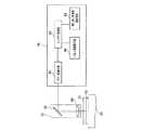
以下、本発明の実施形態を図面を参照して詳細に説明する。図1を参照すると、本発明のSiC基板の分離方法を実施するのに適したレーザー加工装置2の斜視図が示されている。レーザー加工装置2は、静止基台4上にX軸方向に移動可能に搭載された第1スライドブロック6を含んでいる。 Hereinafter, embodiments of the present invention will be described in detail with reference to the drawings. Referring to FIG. 1, a perspective view of a laser processing apparatus 2 suitable for carrying out the method for separating a SiC substrate of the present invention is shown. The laser processing apparatus 2 includes a first slide block 6 mounted on a stationary base 4 so as to be movable in the X-axis direction.
第1スライドブロック6は、ボールねじ8及びパルスモータ10から構成される加工送り機構12により一対のガイドレール14に沿って加工送り方向、即ちX軸方向に移動される。 The first slide block 6 is moved in the machining feed direction, that is, the X-axis direction along the pair of
第1スライドブロック6上には第2スライドブロック16がY軸方向に移動可能に搭載されている。即ち、第2スライドブロック16はボールねじ18及びパルスモータ20から構成される割り出し送り機構22により一対のガイドレール24に沿って割り出し送り方向、即ちY軸方向に移動される。 A
第2スライドブロック16上には吸引保持部26aを有するチャックテーブル26が搭載されている。チャックテーブル26は加工送り機構12及び割り出し送り機構22によりX軸方向及びY軸方向に移動可能であると共に、第2スライドブロック16中に収容されたモータにより回転される。 On the
静止基台4にはコラム28が立設されており、このコラム28にレーザービーム照射機構(レーザービーム照射手段)30が取り付けられている。レーザービーム照射機構30は、ケーシング32中に収容された図2に示すレーザービーム発生ユニット34と、ケーシング32の先端にZ軸方向に移動可能に取り付けられた集光器(レーザーヘッド)36とから構成される。ケーシング32の先端には集光器36とX軸方向に整列して顕微鏡及びカメラを有する撮像ユニット38が取り付けられている。 A
レーザービーム発生ユニット34は、図2に示すように、YAGレーザー又はYVO4レーザーを発振するレーザー発振器40と、繰り返し周波数設定手段42と、パルス幅調整手段44と、パワー調整手段46とを含んでいる。特に図示しないが、レーザー発振器40はブリュースター窓を有しており、レーザー発振器40から出射されるレーザービームは直線偏光のレーザービームである。 As shown in FIG. 2, the laser
レーザービーム発生ユニット34のパワー調整手段46により所定パワーに調整されたパルスレーザービームは、集光器36のミラー48により反射され、更に集光レンズ50によりチャックテーブル26に保持された被加工物であるSiCウエーハ31の内部に集光点を位置づけられて照射される。 The pulse laser beam adjusted to a predetermined power by the power adjusting means 46 of the laser
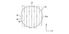
図3(A)を参照すると、SiCインゴット(以下、単にインゴットと略称することがある)11の斜視図が示されている。図3(B)は図3(A)に示したSiCインゴット11の正面図である。 Referring to FIG. 3A, a perspective view of a SiC ingot (hereinafter sometimes simply referred to as an ingot) 11 is shown. FIG. 3B is a front view of
インゴット11は、第1の面(上面)11aと第1の面11aと反対側の第2の面(下面)11bを有している。インゴット11の上面11aは、レーザービームの照射面となるため鏡面に研磨されている。 The
インゴット11は、第1のオリエンテーションフラット13と、第1のオリエンテーションフラット13に直交する第2のオリエンテーションフラット15を有している。第1のオリエンテーションフラット13の長さは第2のオリエンテーションフラット15の長さより長く形成されている。 The
インゴット11は、上面11aの垂線17に対して第2のオリエンテーションフラット15方向にオフ角α傾斜したc軸19と、c軸19に直交するc面21を有している。c面21はインゴット11の上面11aに対してオフ角α傾斜している。一般的に、SiCインゴット11等の六方晶単結晶インゴットでは、短い第2のオリエンテーションフラット15の伸長方向に直交する方向がc軸の傾斜方向である。 The
c面21はインゴット11中にインゴット11の分子レベルで無数に設定される。本実施形態では、オフ角αは4°に設定されている。しかし、オフ角αは4°に限定されるものではなく、例えば1°〜6°の範囲で自由に設定してインゴット11を製造することができる。 The c-
図1を再び参照すると、静止基台4の左側にはコラム52が固定されており、このコラム52にはコラム52に形成された開口53を介して押さえ機構54が上下方向に移動可能に搭載されている。 Referring to FIG. 1 again, a
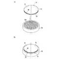
図4を参照すると、SiC基板31の第1の面(上面)31aに粘着テープ41を貼着し、第2の面(下面)31bに保持部材43を貼着する様子を示す斜視図が示されている。粘着テープ41は透明であり、例えば、腰の強いポリエチレンテレフタレート(PET)等の基材に粘着層を配設して構成されている。 Referring to FIG. 4, a perspective view showing a state where the
保持部材43は透明である必要がなく、例えば、ガラス、シリコンウエーハ等から形成されており、接着剤によりSiC基板31の下面31bに貼着される。粘着テープを保持部材43の代わりに使用しても良い。SiC基板31は、図3に示すSiCインゴット11をワイヤーソー等でスライスしたものであり、約700μmの厚みを有している。 The holding
SiC基板31は、第1のオリエンテーションフラット37と、第1のオリエンテーションフラット37に直交する第2のオリエンテーションフラット39を有している。第1のオリエンテーションフラット37の長さは第2のオリエンテーションフラット39の長さより長く形成されている。 The
ここで、SiC基板31は、図3に示したSiCインゴット11をワイヤーソーでスライスしたものであるため、第1のオリエンテーションフラット37はインゴット11の第1のオリエンテーションフラット13に対応し、第2のオリエンテーションフラット39はインゴット11の第2のオリエンテーションフラット15に対応するものである。 Here, since the
そして、SiC基板31は、上面31aの垂線に対して第2のオリエンテーションフラット39方向にオフ角α傾斜したc軸19と、c軸19に直交するc面21を有している(図3参照)。
c面21はSiC基板31の上面31aに対してオフ角α傾斜している。このSiC基板31では、短い第2のオリエンテーションフラット39の伸長方向に直交する方向がc軸19の傾斜方向である。 The
SiC基板31に粘着テープ41及び保持部材43を貼着した後、図5(A)に示すように、保持部材43側を下にしてSiC基板31をチャックテーブル26上に載置し、チャックテーブル26の吸引保持部26aに負圧を作用させて、図5(B)に示すように、SiC基板31を保持部材43を介してチャックテーブル26で吸引保持し、粘着テープ41を露出させる。 After adhering the
そして、図6及び図7に示すように、SiC基板31の第2のオリエンテーションフラット39がX軸方向に整列するようにSiC基板31を保持したチャックテーブル26を回転させる。 6 and 7, the chuck table 26 holding the
即ち、図7に示すように、オフ角αが形成される方向Y1、換言すると、SiC基板31の上面31aの垂線17に対してc軸19の上面31aとの交点19aが存在する方向に直交する方向、即ち、第2のオリエンテーションフラット39に平行な矢印A方向がX軸方向に整列するようにチャックテーブル26を回転する。 That is, as shown in FIG. 7, the direction Y1 in which the off-angle α is formed, in other words, perpendicular to the perpendicular 17 of the
これにより、オフ角αが形成される方向に直交する方向Aに沿ってレーザービームが走査される。換言すると、オフ角αが形成される方向Y1に直交するA方向がチャックテーブル26の加工送り方向となる。 Thereby, the laser beam is scanned along the direction A orthogonal to the direction in which the off angle α is formed. In other words, the A direction orthogonal to the direction Y1 in which the off angle α is formed is the machining feed direction of the chuck table 26.
本発明のSiC基板の分離方法では、集光器36から出射されるレーザービームの走査方向を、ウエーハ31のオフ角αが形成される方向Y1に直交する矢印A方向としたことが重要である。 In the SiC substrate separation method of the present invention, it is important that the scanning direction of the laser beam emitted from the
即ち、本発明のSiC基板の分離方法は、レーザービームの走査方向を上述したような方向に設定することにより、SiC基板31の内部に形成される改質層から伝播するクラックがc面21に沿って非常に長く伸長することを見出した点に特徴がある。 That is, in the method for separating a SiC substrate of the present invention, the crack propagating from the modified layer formed inside the
本実施形態のSiC基板の分離方法では、まず、チャックテーブル26に保持されたSiC基板31及び粘着テープ41に対して透過性を有する波長(例えば1064nmの波長)のレーザービームの集光点をSiC基板31の内部に位置付けると共に、集光点とSiC基板31とを相対的に移動しながらレーザービームを粘着テープ41に照射し、SiC基板31の第1の面(上面)31aに平行な改質層45及び改質層45からc面21に沿って伝播するクラック47を形成して分離起点とする分離起点形成ステップを実施する。 In the SiC substrate separation method of the present embodiment, first, a condensing point of a laser beam having a wavelength (for example, a wavelength of 1064 nm) having transparency with respect to the
この分離起点形成ステップは、図7に示すように、SiC基板31の第1の面(上面)31aに対してc軸19がオフ角α分傾き、c面21と第1の面(上面)31aとにオフ角α形成される方向、即ち、図7の矢印Y1方向に直交する方向、即ちA方向にレーザービームの集光点を相対的に移動して、図8に示すように、SiC基板31の内部に改質層45及び改質層45からc面21に沿って伝播するクラック47を形成する改質層形成ステップと、図9に示すように、オフ角が形成される方向、即ちY軸方向に集光点を相対的に移動して所定量インデックス送りするインデックスステップとを含んでいる。 As shown in FIG. 7, in this separation starting point formation step, the c-
図8及び図9に示すように、改質層45をX軸方向に直線状に形成すると、改質層45の両側からc面21に沿ってクラック47が伝播して形成される。本実施形態のSiC基板の分離方法では、直線状の改質層45からc面21方向に伝播して形成されるクラック47の幅を計測し、集光点のインデックス量を設定するインデックス量設定ステップを含む。 As shown in FIGS. 8 and 9, when the modified
インデックス量設定ステップにおいて、図8に示すように、直線状の改質層45からc面方向に伝播して改質層45の片側に形成されるクラック47の幅をW1とした場合、インデックスすべき所定量W2は、W1以上2W1以下に設定される。 In the index amount setting step, as shown in FIG. 8, when the width of the
ここで、好ましい実施形態の、分離起点形成ステップのレーザー加工条件は以下のように設定される。 Here, the laser processing conditions in the separation starting point forming step of the preferred embodiment are set as follows.
光源 :Nd:YAGパルスレーザー
波長 :1064nm
繰り返し周波数 :80kHz
平均出力 :3.2W
パルス幅 :4ns
スポット径 :10μm
集光レンズの開口数(NA) :0.45
インデックス量 :400μmLight source: Nd: YAG pulse laser Wavelength: 1064 nm
Repetition frequency: 80 kHz
Average output: 3.2W
Pulse width: 4 ns
Spot diameter: 10 μm
Numerical aperture (NA) of condenser lens: 0.45
Index amount: 400 μm
上述したレーザー加工条件においては、図8において、改質層45からc面21に沿って伝播するクラック47の幅W1が略250μmに設定され、インデックス量W2が400μmに設定される。 Under the laser processing conditions described above, in FIG. 8, the width W1 of the
しかし、レーザービームの平均出力は3.2Wに限定されるものではなく、本実施形態の加工方法では、平均出力を2W〜4.5Wに設定して良好な結果が得られた。平均出力2Wの場合、クラック25の幅W1は略100μmとなり、平均出力4.5Wの場合には、クラック25の幅W1は略350μmとなった。 However, the average output of the laser beam is not limited to 3.2 W, and with the processing method of this embodiment, good results were obtained by setting the average output to 2 W to 4.5 W. When the average output was 2 W, the width W1 of the crack 25 was approximately 100 μm, and when the average output was 4.5 W, the width W1 of the crack 25 was approximately 350 μm.
平均出力が2W未満の場合及び4.5Wより大きい場合には、SiC基板31の内部に良好な改質層45を形成することができないため、照射するレーザービームの平均出力は2W〜4.5Wの範囲内が好ましく、本実施形態では平均出力3.2Wのレーザービームをウエーハ31に照射した。 When the average output is less than 2 W and greater than 4.5 W, the good modified
図10を参照すると、レーザービームの走査方向を説明する模式図が示されている。分離起点形成ステップは往路X1及び復路X2で実施され、往路X1でSiC基板31に改質層45を形成したレーザービームの集光点は、所定量インデックスされた後、復路X2でSiC基板31に改質層45を形成する。 Referring to FIG. 10, a schematic diagram illustrating the scanning direction of the laser beam is shown. The separation starting point forming step is performed in the forward path X1 and the return path X2, and the condensing point of the laser beam that has formed the modified
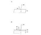
次に、図11(A)に示すように、レーザービームLBをSiC基板31に直接照射する場合と、図11(B)に示すように、SiC基板31に貼着された粘着テープ41にレーザービームLBを照射する場合についてのフレネル反射強度について考察する。 Next, as shown in FIG. 11A, the laser beam LB is directly irradiated onto the
物体Aから物体BにレーザービームLBが入射するものとして、物体Aの屈折率をn1、物体Bの屈折率をn2とし、入射光の強さをI0、反射光の強さをIとすると、フレネル反射強度Iは、I=I0{(n2−n1)/(n2+n1)}2で表される。Assuming that the laser beam LB is incident from the object A to the object B, the refractive index of the object A is n1, the refractive index of the object B is n2, the intensity of the incident light is I0 , and the intensity of the reflected light is I. , Fresnel reflection intensity I is represented by I = I0 {(n2−n1) / (n2 + n1)}2 .
ここで、図11(A)の場合には、物体Aは空気であるため、n1=1であり、物体2はSiC基板31であるため、n2=2.6となる。従って、反射光R1の強さI1はI1=100{(2.6−1)/(2.6+1)}2=19.8%となる。すなわち、SiC基板31を透過するレーザービームLBの強さは100−19.8=80.2%となる。In the case of FIG. 11A, since the object A is air, n1 = 1, and the object 2 is the
一方、図11(B)に示す本発明実施形態の構成では、SiC基板31の上面に透明な粘着テープ41が貼着されている。この場合には、物体1は空気であるため、n1=1、物体2は粘着テープ41であるため、n2=1.5、物体3はSiC基板31であるため、n3=2.6となる。 On the other hand, in the configuration of the embodiment of the present invention shown in FIG. 11 (B), a transparent
まず粘着テープ41の上面での反射光R2のフレネル反射強度I2を求める。I2=I0{(n2−n1)/(n2+n1)}2=100{(1.5−1)/(1.5+1)}2=4%となる。従って、粘着テープ41を透過するレーザービームの強さは入射レーザービームLBの96%となる。First determine the Fresnel reflection intensity I2 of the reflected light R2 at the upper surface of the
次に、SiC基板31の上面で反射する反射光R3のフレネル反射強度をI3とすると、I3=I2{(n3−n2)/(n3+n2)}2=96{(2.6−1.5)/(2.6+1.5)}2=6.9%となる。従って、SiC基板31を透過するレーザービームの強さは粘着テープ41に照射されたレーザービームLBの89.1%となる。Next, assuming that the Fresnel reflection intensity of the reflected light R3 reflected from the upper surface of the
以上の考察から、図11(B)に示すように、SiC基板31の上面に透明な粘着テープ41を貼着すると、図11(A)に示すSiC基板31にレーザービームLBを直接入射する場合に比較して、SiC基板31を透過するレーザービームの強さが89.1−80.2=8.9%向上する。 From the above consideration, when the transparent
このように、屈折率が大きく相違する物体1から物体2にレーザービームを直接入射する場合に比較して、物体1の屈折率n1と物体3の屈折率n3の間の屈折率n2を有する物体2を介して物体3にレーザービームを入射すると、物体3を透過するレーザービームの強度が向上することになる。 In this way, an object having a refractive index n2 between the refractive index n1 of the object 1 and the refractive index n3 of the object 3 as compared with the case where the laser beam is directly incident on the object 2 from the object 1 having a significantly different refractive index. When the laser beam is incident on the object 3 via 2, the intensity of the laser beam transmitted through the object 3 is improved.
所定量インデックス送りしながら、SiC基板31の内部に複数の改質層45及び改質層45からc面21に沿って伸びるクラック47の形成が終了したならば、外力を付与して改質層45及びクラック47からなる分離起点からSiC基板31を2つに分離する分離ステップを実施する。 When the formation of the plurality of modified
この分離ステップは、例えば図1及び図12に示すような押圧機構54により実施する。押圧機構54は、コラム52内に内蔵された移動機構により上下方向に移動するヘッド56と、ヘッド56に対して、図12(B)に示すように、矢印R方向に回転される押圧部材58とを含んでいる。 This separation step is performed by a
図12(A)に示すように、押圧機構54をチャックテーブル26に保持されたSiC基板31の上方に位置付け、図12(B)に示すように、押圧部材58をSiC基板31の上面31aに貼着された粘着テープ41に圧接するまでヘッド56を下降する。 As shown in FIG. 12A, the
押圧部材58を粘着テープ41に圧接した状態で、押圧部材58を矢印R方向に回転すると、SiC基板31にはねじり応力が発生し、改質層45及びクラック47が形成された分離起点からSiC基板31が破断され、SiC基板31を2つに分離することができる。 When the pressing
上述した実施形態では、押圧機構54を用いてSiC基板31を2つに分離しているが、SiC基板31の第1の面(上面)31aに粘着テープ41が貼着され、第2の面(下面)31bに保持部材43が貼着されており、SiC基板31の全面に改質層45及びクラック47とからなる分離起点が形成されているため、粘着テープ41及び保持部材43を互いに反対方向に引っ張ることによっても、SiC基板31を2つに分離することができる。 In the embodiment described above, the
分離ステップを実施すると、チャックテーブル26に保持されたSiC基板31Aの分離面49には改質層45とクラック47の一部が残存することとなり、図13及び図14に示すように、分離面49には微細な凹凸が形成される。従って、本発明のSiC基板の分離方法では、SiC基板31の分離起点となった面を研削砥石によって研削して平坦化する平坦化ステップを実施する。 When the separation step is performed, a part of the modified
この平坦化ステップでは、図14に示すように、研削装置のチャックテーブル58で保持部材43を介してSiC基板31Aを吸引保持して分離面49を露出させる。研削装置の研削ユニット60は、モータにより回転駆動されるスピンドル62と、スピンドル62の先端に固定されたホイールマウント64と、ホイールマウント64に複数のねじ68により着脱可能に装着された研削ホイール66とを含んでいる。研削ホイール66は、環状のホイール基台70と、ホイール基台70の下端部外周に固着された複数の研削砥石72とから構成されている。 In this flattening step, as shown in FIG. 14, the
平坦化ステップでは、チャックテーブル58を矢印aで示す方向に例えば300rpmで回転しつつ、研削ホイール66を矢印bで示す方向に例えば6000rpmで回転させると共に、研削ユニット送り機構を駆動して研削ホイール66の研削砥石72をSiC基板31Aの分離面49に接触させる。 In the flattening step, while rotating the chuck table 58 in the direction indicated by arrow a at 300 rpm, for example, the grinding
そして、研削ホイール66を所定の研削送り速度(例えば0.1μm/s)で下方に所定量研削送りしながらSiC基板31Aの分離面49を研削して平坦化する。これにより、図15に示すように、SiC基板31Aの第1の面(上面)31aは残存していた改質層45及びクラック47が除去されて平坦面となる。 Then, the
分離されたSiC基板31Aの上面31aを研削して平坦化する場合は、SiC基板31Aの上面31aを1〜5μm程度研削すればよく、研削砥石72の摩耗量を4〜25μm程度に抑えることができる。 When the
図13に示すように、SiC基板31Aから分離されたSiC基板31Bについても、研削装置のチャックテーブル58で粘着テープ41側を吸引保持しながらSiC基板31Bの分離面を研削ホイール66で研削することにより、分離面に残存していた改質層45及びクラック47を除去して分離面を平坦面とすることができる。 As shown in FIG. 13, with respect to the
上述した実施形態では、本発明のSiC基板の分離方法を、改質層45及びクラック47とからなる分離起点をc面に沿って形成する実施形態について説明したが、本発明のSiC基板の分離方法では、改質層45及びクラック47とからなる分離起点が形成されたSiC基板31は、粘着テープ41及び保持部材43により両側から補強されているため、改質層45及びクラック47とからなる分離起点がc面に沿って形成されていない特許文献2に開示されたような方法にも同様に適用することができる。 In the above-described embodiment, the SiC substrate separation method of the present invention has been described with respect to the embodiment in which the separation starting point composed of the modified
2 レーザー加工装置
11 SiCインゴット
13,37 第1のオリエンテーションフラット
15,39 第2のオリエンテーションフラット
19 c軸
21 c面
30 レーザービーム照射ユニット
31 SiC基板
36 集光器(レーザーヘッド)
41 粘着テープ
43 保持部材
45 改質層
47 クラック
49 分離面
66 研削ホイール
72 研削砥石2
41
Claims (4)
Translated fromJapanese該第1の面に透明な粘着テープを貼着する粘着テープ貼着ステップと、
該第2の面に保持部材を貼着する保持部材貼着ステップと、
該粘着テープ貼着ステップ及び該保持部材貼着ステップを実施した後、SiC基板及び該粘着テープに対して透過性を有する波長のレーザービームの集光点を該粘着テープ側からSiC基板の内部に位置付けると共に、該集光点とSiC基板とを相対的に移動しながらレーザービームを該粘着テープに照射し、該第1の面に平行な改質層及びクラックとを形成して分離起点とする分離起点形成ステップと、
該分離起点形成ステップを実施した後、外力を付与して該分離起点から該粘着テープと共に該第1の面を有するSiC基板を該第2の面を有するSiC基板から分離する分離ステップと、
を備えたことを特徴とするSiC基板の分離方法。A SiC substrate separation method for separating an SiC substrate having a first surface and a second surface opposite to the first surface into at least two sheets,
An adhesive tape adhering step for adhering a transparent adhesive tape to the first surface;
A holding member attaching step for attaching the holding member to the second surface;
After performing the adhesive tape adhering step and the holding member adhering step, the focusing point of the laser beam having a wavelength transmissive to the SiC substrate and the adhesive tape is moved from the adhesive tape side to the inside of the SiC substrate. Positioning and irradiating the adhesive tape with a laser beam while relatively moving the light condensing point and the SiC substrate, forming a modified layer and cracks parallel to the first surface as separation starting points A separation origin formation step;
A separation step of separating the SiC substrate having the first surface together with the adhesive tape from the separation starting point by separating the SiC substrate having the second surface from the separation starting point by applying an external force after performing the separation starting point forming step;
A method for separating a SiC substrate, comprising:
該第1の面に透明な粘着テープを貼着する粘着テープ貼着ステップと、
該第2の面に保持部材を貼着する保持部材貼着ステップと、
該粘着テープ貼着ステップ及び該保持部材貼着ステップを実施した後、SiC基板及び該粘着テープに対して透過性を有する波長のレーザービームの集光点を該粘着テープ側からSiC基板の内部に位置付けると共に、該集光点とSiC基板とを相対的に移動しながらレーザービームを該粘着テープに照射し、該第1の面に平行な改質層及びクラックとを形成して分離起点とする分離起点形成ステップと、
該分離起点形成ステップを実施した後、外力を付与して該分離起点から該粘着テープと共に該第1の面を有するSiC基板を該第2の面を有するSiC基板から分離する分離ステップと、を備え、
該分離起点形成ステップは、該第1の面の垂線に対して該c軸がオフ角分傾き、該第1の面と該c面との間にオフ角が形成される方向と直交する方向にレーザービームの集光点を相対的に移動して直線状の改質層を形成する改質層形成ステップと、
該オフ角が形成される方向に該集光点を相対的に移動して所定量インデックスするインデックスステップと、を含むことを特徴とするSiC基板の分離方法。SiC having a first surface, a second surface opposite to the first surface, a c-axis extending from the first surface to the second surface, and a c-plane orthogonal to the c-axis A SiC substrate separation method for separating a substrate into at least two substrates,
An adhesive tape adhering step for adhering a transparent adhesive tape to the first surface;
A holding member attaching step for attaching the holding member to the second surface;
After performing the adhesive tape adhering step and the holding member adhering step, the focusing point of the laser beam having a wavelength transmissive to the SiC substrate and the adhesive tape is moved from the adhesive tape side to the inside of the SiC substrate. Positioning and irradiating the adhesive tape with a laser beam while relatively moving the light condensing point and the SiC substrate, forming a modified layer and cracks parallel to the first surface as separation starting points A separation origin formation step;
A separation step of separating the SiC substrate having the first surface together with the adhesive tape from the separation origin by separating the SiC substrate having the second surface by applying an external force after the separation starting point forming step is performed; Prepared,
The separation starting point forming step includes a direction orthogonal to a direction in which the c-axis is inclined by an off-angle with respect to the normal of the first surface and an off-angle is formed between the first surface and the c-plane. A modified layer forming step of forming a linear modified layer by relatively moving the condensing point of the laser beam;
And a step of indexing a predetermined amount by relatively moving the condensing point in a direction in which the off-angle is formed.
Priority Applications (8)
| Application Number | Priority Date | Filing Date | Title |
|---|---|---|---|
| JP2015222369AJP6562819B2 (en) | 2015-11-12 | 2015-11-12 | Method for separating SiC substrate |
| TW105132904ATWI706454B (en) | 2015-11-12 | 2016-10-12 | Separation method of silicon carbide (SiC) substrate |
| MYPI2016703882AMY180611A (en) | 2015-11-12 | 2016-10-21 | Sic substrate separating method |
| SG10201608938WASG10201608938WA (en) | 2015-11-12 | 2016-10-25 | SiC SUBSTRATE SEPARATING METHOD |
| KR1020160141140AKR102475682B1 (en) | 2015-11-12 | 2016-10-27 | METHOD OF SEPARATING SiC SUBSTRATE |
| CN201610930017.6ACN107030392B (en) | 2015-11-12 | 2016-10-31 | Separation method of SiC substrate |
| US15/342,583US10105792B2 (en) | 2015-11-12 | 2016-11-03 | SiC substrate separating method |
| DE102016222200.7ADE102016222200B4 (en) | 2015-11-12 | 2016-11-11 | SIC SUBSTRATE SEPARATION PROCESS |
Applications Claiming Priority (1)
| Application Number | Priority Date | Filing Date | Title |
|---|---|---|---|
| JP2015222369AJP6562819B2 (en) | 2015-11-12 | 2015-11-12 | Method for separating SiC substrate |
Publications (2)
| Publication Number | Publication Date |
|---|---|
| JP2017092314Atrue JP2017092314A (en) | 2017-05-25 |
| JP6562819B2 JP6562819B2 (en) | 2019-08-21 |
Family
ID=58640404
Family Applications (1)
| Application Number | Title | Priority Date | Filing Date |
|---|---|---|---|
| JP2015222369AActiveJP6562819B2 (en) | 2015-11-12 | 2015-11-12 | Method for separating SiC substrate |
Country Status (8)
| Country | Link |
|---|---|
| US (1) | US10105792B2 (en) |
| JP (1) | JP6562819B2 (en) |
| KR (1) | KR102475682B1 (en) |
| CN (1) | CN107030392B (en) |
| DE (1) | DE102016222200B4 (en) |
| MY (1) | MY180611A (en) |
| SG (1) | SG10201608938WA (en) |
| TW (1) | TWI706454B (en) |
Cited By (18)
| Publication number | Priority date | Publication date | Assignee | Title |
|---|---|---|---|---|
| WO2018163752A1 (en)* | 2017-03-06 | 2018-09-13 | 信越半導体株式会社 | Method for manufacturing wafer |
| WO2019044530A1 (en)* | 2017-09-04 | 2019-03-07 | リンテック株式会社 | Thinned plate member production method and production device |
| WO2019044588A1 (en)* | 2017-09-04 | 2019-03-07 | リンテック株式会社 | Thinned plate member production method and thinned plate member production device |
| US10388526B1 (en) | 2018-04-20 | 2019-08-20 | Semiconductor Components Industries, Llc | Semiconductor wafer thinning systems and related methods |
| JP2019161166A (en)* | 2018-03-16 | 2019-09-19 | 株式会社ディスコ | Wafer processing method |
| US10468304B1 (en) | 2018-05-31 | 2019-11-05 | Semiconductor Components Industries, Llc | Semiconductor substrate production systems and related methods |
| JP2020035873A (en)* | 2018-08-29 | 2020-03-05 | 株式会社ディスコ | Processing method of SiC substrate |
| WO2020066492A1 (en)* | 2018-09-25 | 2020-04-02 | 東京エレクトロン株式会社 | Substrate processing system and substrate processing method |
| JPWO2021006091A1 (en)* | 2019-07-10 | 2021-01-14 | ||
| US10896815B2 (en) | 2018-05-22 | 2021-01-19 | Semiconductor Components Industries, Llc | Semiconductor substrate singulation systems and related methods |
| US11121035B2 (en) | 2018-05-22 | 2021-09-14 | Semiconductor Components Industries, Llc | Semiconductor substrate processing methods |
| JP2021137905A (en)* | 2020-03-04 | 2021-09-16 | 株式会社ディスコ | Grinding method for workpieces |
| JPWO2020129732A1 (en)* | 2018-12-21 | 2021-10-21 | 東京エレクトロン株式会社 | Substrate processing equipment and substrate processing method |
| JPWO2020129733A1 (en)* | 2018-12-21 | 2021-10-21 | 東京エレクトロン株式会社 | Substrate processing equipment and substrate processing method |
| JPWO2020129730A1 (en)* | 2018-12-21 | 2021-10-28 | 東京エレクトロン株式会社 | Substrate processing equipment and substrate processing method |
| JP2022180079A (en)* | 2021-05-24 | 2022-12-06 | 株式会社ディスコ | Substrate separation method |
| US11830771B2 (en) | 2018-05-31 | 2023-11-28 | Semiconductor Components Industries, Llc | Semiconductor substrate production systems and related methods |
| US11854889B2 (en) | 2018-05-24 | 2023-12-26 | Semiconductor Components Industries, Llc | Die cleaning systems and related methods |
Families Citing this family (15)
| Publication number | Priority date | Publication date | Assignee | Title |
|---|---|---|---|---|
| JP6429715B2 (en)* | 2015-04-06 | 2018-11-28 | 株式会社ディスコ | Wafer generation method |
| JP6478821B2 (en)* | 2015-06-05 | 2019-03-06 | 株式会社ディスコ | Wafer generation method |
| JP6781639B2 (en)* | 2017-01-31 | 2020-11-04 | 株式会社ディスコ | Wafer generation method |
| JP6920849B2 (en)* | 2017-03-27 | 2021-08-18 | 株式会社荏原製作所 | Substrate processing method and equipment |
| WO2018235843A1 (en) | 2017-06-19 | 2018-12-27 | ローム株式会社 | Method of manufacturing semiconductor device and wafer bonding structure |
| JP7009194B2 (en)* | 2017-12-12 | 2022-01-25 | 株式会社ディスコ | Wafer generator and transport tray |
| JP7235456B2 (en)* | 2018-08-14 | 2023-03-08 | 株式会社ディスコ | Semiconductor substrate processing method |
| JP7106217B2 (en)* | 2018-08-22 | 2022-07-26 | 株式会社ディスコ | Method and apparatus for detecting facet area |
| JP7187215B2 (en)* | 2018-08-28 | 2022-12-12 | 株式会社ディスコ | SiC substrate processing method |
| US10562130B1 (en) | 2018-12-29 | 2020-02-18 | Cree, Inc. | Laser-assisted method for parting crystalline material |
| US11024501B2 (en) | 2018-12-29 | 2021-06-01 | Cree, Inc. | Carrier-assisted method for parting crystalline material along laser damage region |
| US10576585B1 (en) | 2018-12-29 | 2020-03-03 | Cree, Inc. | Laser-assisted method for parting crystalline material |
| US10611052B1 (en) | 2019-05-17 | 2020-04-07 | Cree, Inc. | Silicon carbide wafers with relaxed positive bow and related methods |
| JP7072180B1 (en)* | 2021-12-20 | 2022-05-20 | 有限会社サクセス | Manufacturing method and equipment for semiconductor crystal wafers |
| CN119328911A (en)* | 2023-10-16 | 2025-01-21 | 西湖仪器(杭州)技术有限公司 | A crack propagation method for solid materials and a laser slicing method |
Citations (6)
| Publication number | Priority date | Publication date | Assignee | Title |
|---|---|---|---|---|
| JP2010021398A (en)* | 2008-07-11 | 2010-01-28 | Disco Abrasive Syst Ltd | Method of treating wafer |
| JP2011060862A (en)* | 2009-09-07 | 2011-03-24 | Saitama Univ | Substrate slicing method |
| JP2011192934A (en)* | 2010-03-16 | 2011-09-29 | Disco Corp | Division method for workpiece |
| JP2013041908A (en)* | 2011-08-12 | 2013-02-28 | Disco Abrasive Syst Ltd | Method of dividing optical device wafer |
| JP2013049161A (en)* | 2011-08-30 | 2013-03-14 | Hamamatsu Photonics Kk | Method of cutting workpiece |
| JP2015115573A (en)* | 2013-12-16 | 2015-06-22 | 株式会社東京精密 | Laser dicing method |
Family Cites Families (12)
| Publication number | Priority date | Publication date | Assignee | Title |
|---|---|---|---|---|
| JP2000094221A (en) | 1998-09-24 | 2000-04-04 | Toyo Advanced Technologies Co Ltd | Electric discharge wire saw |
| JP4659300B2 (en)* | 2000-09-13 | 2011-03-30 | 浜松ホトニクス株式会社 | Laser processing method and semiconductor chip manufacturing method |
| JP3998639B2 (en)* | 2004-01-13 | 2007-10-31 | 株式会社東芝 | Manufacturing method of semiconductor light emitting device |
| US20050217560A1 (en)* | 2004-03-31 | 2005-10-06 | Tolchinsky Peter G | Semiconductor wafers with non-standard crystal orientations and methods of manufacturing the same |
| JP5446325B2 (en)* | 2009-03-03 | 2014-03-19 | 豊田合成株式会社 | Laser processing method and compound semiconductor light emitting device manufacturing method |
| DE102010030358B4 (en)* | 2010-06-22 | 2014-05-22 | Osram Opto Semiconductors Gmbh | Method for separating a substrate wafer |
| JP5875122B2 (en)* | 2011-02-10 | 2016-03-02 | 信越ポリマー株式会社 | Single crystal substrate manufacturing method and internal modified layer forming single crystal member |
| CN103380482B (en)* | 2011-02-10 | 2016-05-25 | 信越聚合物株式会社 | Single crystallization base plate manufacture method and inner upgrading layer form single crystals parts |
| JP6002982B2 (en) | 2011-08-31 | 2016-10-05 | 株式会社フジシール | Pouch container |
| JP6032789B2 (en)* | 2012-02-01 | 2016-11-30 | 信越ポリマー株式会社 | Method for manufacturing single crystal processed member and method for manufacturing single crystal substrate |
| JP6044919B2 (en)* | 2012-02-01 | 2016-12-14 | 信越ポリマー株式会社 | Substrate processing method |
| JP2014041925A (en)* | 2012-08-22 | 2014-03-06 | Hamamatsu Photonics Kk | Method for cutting workpiece |
- 2015
- 2015-11-12JPJP2015222369Apatent/JP6562819B2/enactiveActive
- 2016
- 2016-10-12TWTW105132904Apatent/TWI706454B/enactive
- 2016-10-21MYMYPI2016703882Apatent/MY180611A/enunknown
- 2016-10-25SGSG10201608938WApatent/SG10201608938WA/enunknown
- 2016-10-27KRKR1020160141140Apatent/KR102475682B1/enactiveActive
- 2016-10-31CNCN201610930017.6Apatent/CN107030392B/enactiveActive
- 2016-11-03USUS15/342,583patent/US10105792B2/enactiveActive
- 2016-11-11DEDE102016222200.7Apatent/DE102016222200B4/enactiveActive
Patent Citations (6)
| Publication number | Priority date | Publication date | Assignee | Title |
|---|---|---|---|---|
| JP2010021398A (en)* | 2008-07-11 | 2010-01-28 | Disco Abrasive Syst Ltd | Method of treating wafer |
| JP2011060862A (en)* | 2009-09-07 | 2011-03-24 | Saitama Univ | Substrate slicing method |
| JP2011192934A (en)* | 2010-03-16 | 2011-09-29 | Disco Corp | Division method for workpiece |
| JP2013041908A (en)* | 2011-08-12 | 2013-02-28 | Disco Abrasive Syst Ltd | Method of dividing optical device wafer |
| JP2013049161A (en)* | 2011-08-30 | 2013-03-14 | Hamamatsu Photonics Kk | Method of cutting workpiece |
| JP2015115573A (en)* | 2013-12-16 | 2015-06-22 | 株式会社東京精密 | Laser dicing method |
Cited By (46)
| Publication number | Priority date | Publication date | Assignee | Title |
|---|---|---|---|---|
| WO2018163752A1 (en)* | 2017-03-06 | 2018-09-13 | 信越半導体株式会社 | Method for manufacturing wafer |
| JP2018148042A (en)* | 2017-03-06 | 2018-09-20 | 信越半導体株式会社 | Wafer manufacturing method |
| KR102565070B1 (en)* | 2017-09-04 | 2023-08-08 | 린텍 가부시키가이샤 | Manufacturing method of thinning plate-like member, and manufacturing apparatus |
| WO2019044588A1 (en)* | 2017-09-04 | 2019-03-07 | リンテック株式会社 | Thinned plate member production method and thinned plate member production device |
| CN111095493B (en)* | 2017-09-04 | 2024-04-02 | 琳得科株式会社 | Method and apparatus for manufacturing thin plate-like member |
| JPWO2019044588A1 (en)* | 2017-09-04 | 2020-10-15 | リンテック株式会社 | Manufacturing method of thin plate-shaped member and manufacturing equipment of thin plate-shaped member |
| KR102565071B1 (en)* | 2017-09-04 | 2023-08-08 | 린텍 가부시키가이샤 | Manufacturing method of thinning plate-like member, and manufacturing apparatus of thinning plate-like member |
| JP7231548B2 (en) | 2017-09-04 | 2023-03-01 | リンテック株式会社 | METHOD AND APPARATUS FOR MANUFACTURING THIN PLATE-LIKE MEMBER |
| KR20200044001A (en)* | 2017-09-04 | 2020-04-28 | 린텍 가부시키가이샤 | Manufacturing method of thinned plate-shaped member, and manufacturing apparatus |
| CN111095493A (en)* | 2017-09-04 | 2020-05-01 | 琳得科株式会社 | Method for manufacturing thin plate-like member and device for manufacturing thin plate-like member |
| KR20200047554A (en)* | 2017-09-04 | 2020-05-07 | 린텍 가부시키가이샤 | Method for manufacturing thinned plate-like member, and apparatus for manufacturing thinned plate-like member |
| WO2019044530A1 (en)* | 2017-09-04 | 2019-03-07 | リンテック株式会社 | Thinned plate member production method and production device |
| JPWO2019044530A1 (en)* | 2017-09-04 | 2020-10-22 | リンテック株式会社 | Manufacturing method and manufacturing equipment for thin plate-shaped members |
| JP2019161166A (en)* | 2018-03-16 | 2019-09-19 | 株式会社ディスコ | Wafer processing method |
| US11152211B2 (en) | 2018-04-20 | 2021-10-19 | Semiconductor Components Industries, Llc | Semiconductor wafer thinning systems and related methods |
| US10388526B1 (en) | 2018-04-20 | 2019-08-20 | Semiconductor Components Industries, Llc | Semiconductor wafer thinning systems and related methods |
| US10665458B2 (en) | 2018-04-20 | 2020-05-26 | Semiconductor Components Industries, Llc | Semiconductor wafer thinning systems and related methods |
| US11373859B2 (en) | 2018-05-22 | 2022-06-28 | Semiconductor Components Industries, Llc | Semiconductor substrate singulation systems and related methods |
| US10896815B2 (en) | 2018-05-22 | 2021-01-19 | Semiconductor Components Industries, Llc | Semiconductor substrate singulation systems and related methods |
| US11121035B2 (en) | 2018-05-22 | 2021-09-14 | Semiconductor Components Industries, Llc | Semiconductor substrate processing methods |
| US11823953B2 (en) | 2018-05-22 | 2023-11-21 | Semiconductor Components Industries, Llc | Semiconductor substrate processing methods |
| US12230543B2 (en) | 2018-05-24 | 2025-02-18 | Semiconductor Components Industries, Llc | Die cleaning systems and related methods |
| US11854889B2 (en) | 2018-05-24 | 2023-12-26 | Semiconductor Components Industries, Llc | Die cleaning systems and related methods |
| US11830771B2 (en) | 2018-05-31 | 2023-11-28 | Semiconductor Components Industries, Llc | Semiconductor substrate production systems and related methods |
| US10468304B1 (en) | 2018-05-31 | 2019-11-05 | Semiconductor Components Industries, Llc | Semiconductor substrate production systems and related methods |
| US10770351B2 (en) | 2018-05-31 | 2020-09-08 | Semiconductor Components Industries, Llc | Semiconductor substrate production systems and related methods |
| JP2020035873A (en)* | 2018-08-29 | 2020-03-05 | 株式会社ディスコ | Processing method of SiC substrate |
| JP7201367B2 (en) | 2018-08-29 | 2023-01-10 | 株式会社ディスコ | SiC substrate processing method |
| WO2020066492A1 (en)* | 2018-09-25 | 2020-04-02 | 東京エレクトロン株式会社 | Substrate processing system and substrate processing method |
| JPWO2020066492A1 (en)* | 2018-09-25 | 2021-08-30 | 東京エレクトロン株式会社 | Board processing system and board processing method |
| JP7086201B2 (en) | 2018-09-25 | 2022-06-17 | 東京エレクトロン株式会社 | Board processing system and board processing method |
| JP7287982B2 (en) | 2018-12-21 | 2023-06-06 | 東京エレクトロン株式会社 | SUBSTRATE PROCESSING APPARATUS AND SUBSTRATE PROCESSING METHOD |
| JP7208260B2 (en) | 2018-12-21 | 2023-01-18 | 東京エレクトロン株式会社 | SUBSTRATE PROCESSING APPARATUS AND SUBSTRATE PROCESSING METHOD |
| JP7203863B2 (en) | 2018-12-21 | 2023-01-13 | 東京エレクトロン株式会社 | SUBSTRATE PROCESSING APPARATUS AND SUBSTRATE PROCESSING METHOD |
| JPWO2020129730A1 (en)* | 2018-12-21 | 2021-10-28 | 東京エレクトロン株式会社 | Substrate processing equipment and substrate processing method |
| JPWO2020129733A1 (en)* | 2018-12-21 | 2021-10-21 | 東京エレクトロン株式会社 | Substrate processing equipment and substrate processing method |
| JPWO2020129732A1 (en)* | 2018-12-21 | 2021-10-21 | 東京エレクトロン株式会社 | Substrate processing equipment and substrate processing method |
| JP7229353B2 (en) | 2019-07-10 | 2023-02-27 | 東京エレクトロン株式会社 | Separation device and separation method |
| JPWO2021006091A1 (en)* | 2019-07-10 | 2021-01-14 | ||
| WO2021006091A1 (en)* | 2019-07-10 | 2021-01-14 | 東京エレクトロン株式会社 | Separator and separation method |
| CN114080663A (en)* | 2019-07-10 | 2022-02-22 | 东京毅力科创株式会社 | Separation device and separation method |
| JP7405649B2 (en) | 2020-03-04 | 2023-12-26 | 株式会社ディスコ | Grinding method of workpiece |
| JP2021137905A (en)* | 2020-03-04 | 2021-09-16 | 株式会社ディスコ | Grinding method for workpieces |
| JP2022180079A (en)* | 2021-05-24 | 2022-12-06 | 株式会社ディスコ | Substrate separation method |
| US12304109B2 (en) | 2021-05-24 | 2025-05-20 | Disco Corporation | Method of separating wafer |
| JP7731221B2 (en) | 2021-05-24 | 2025-08-29 | 株式会社ディスコ | How to separate the board |
Also Published As
| Publication number | Publication date |
|---|---|
| CN107030392B (en) | 2020-02-21 |
| DE102016222200B4 (en) | 2025-09-11 |
| CN107030392A (en) | 2017-08-11 |
| KR20170055909A (en) | 2017-05-22 |
| TWI706454B (en) | 2020-10-01 |
| US20170136572A1 (en) | 2017-05-18 |
| SG10201608938WA (en) | 2017-06-29 |
| US10105792B2 (en) | 2018-10-23 |
| TW201729275A (en) | 2017-08-16 |
| JP6562819B2 (en) | 2019-08-21 |
| MY180611A (en) | 2020-12-03 |
| DE102016222200A1 (en) | 2017-05-18 |
| KR102475682B1 (en) | 2022-12-07 |
Similar Documents
| Publication | Publication Date | Title |
|---|---|---|
| JP6562819B2 (en) | Method for separating SiC substrate | |
| JP6482425B2 (en) | Thinning method of wafer | |
| JP6472347B2 (en) | Thinning method of wafer | |
| JP6486239B2 (en) | Wafer processing method | |
| JP6486240B2 (en) | Wafer processing method | |
| JP6482423B2 (en) | Wafer generation method | |
| JP6456228B2 (en) | Thin plate separation method | |
| JP6395634B2 (en) | Wafer generation method | |
| JP6358941B2 (en) | Wafer generation method | |
| JP6604891B2 (en) | Wafer generation method | |
| JP6472333B2 (en) | Wafer generation method | |
| JP6399913B2 (en) | Wafer generation method | |
| JP6429715B2 (en) | Wafer generation method | |
| JP6395633B2 (en) | Wafer generation method | |
| JP6391471B2 (en) | Wafer generation method | |
| JP6358940B2 (en) | Wafer generation method | |
| JP6395632B2 (en) | Wafer generation method | |
| JP6444249B2 (en) | Wafer generation method | |
| JP6366485B2 (en) | Wafer generation method | |
| JP6355540B2 (en) | Wafer generation method | |
| JP2016127186A (en) | Wafer generation method | |
| JP6472332B2 (en) | Wafer generation method | |
| JP6366486B2 (en) | Wafer generation method |
Legal Events
| Date | Code | Title | Description |
|---|---|---|---|
| A621 | Written request for application examination | Free format text:JAPANESE INTERMEDIATE CODE: A621 Effective date:20180928 | |
| A131 | Notification of reasons for refusal | Free format text:JAPANESE INTERMEDIATE CODE: A131 Effective date:20190507 | |
| A977 | Report on retrieval | Free format text:JAPANESE INTERMEDIATE CODE: A971007 Effective date:20190426 | |
| A521 | Request for written amendment filed | Free format text:JAPANESE INTERMEDIATE CODE: A523 Effective date:20190703 | |
| TRDD | Decision of grant or rejection written | ||
| A01 | Written decision to grant a patent or to grant a registration (utility model) | Free format text:JAPANESE INTERMEDIATE CODE: A01 Effective date:20190723 | |
| A61 | First payment of annual fees (during grant procedure) | Free format text:JAPANESE INTERMEDIATE CODE: A61 Effective date:20190723 | |
| R150 | Certificate of patent or registration of utility model | Ref document number:6562819 Country of ref document:JP Free format text:JAPANESE INTERMEDIATE CODE: R150 | |
| R250 | Receipt of annual fees | Free format text:JAPANESE INTERMEDIATE CODE: R250 | |
| R250 | Receipt of annual fees | Free format text:JAPANESE INTERMEDIATE CODE: R250 | |
| R250 | Receipt of annual fees | Free format text:JAPANESE INTERMEDIATE CODE: R250 | |
| R250 | Receipt of annual fees | Free format text:JAPANESE INTERMEDIATE CODE: R250 |