JP2017046559A - Non-contact power supply system and power reception device - Google Patents
Non-contact power supply system and power reception deviceDownload PDFInfo
- Publication number
- JP2017046559A JP2017046559AJP2015169841AJP2015169841AJP2017046559AJP 2017046559 AJP2017046559 AJP 2017046559AJP 2015169841 AJP2015169841 AJP 2015169841AJP 2015169841 AJP2015169841 AJP 2015169841AJP 2017046559 AJP2017046559 AJP 2017046559A
- Authority
- JP
- Japan
- Prior art keywords
- power
- power receiving
- coil
- power transmission
- impedance
- Prior art date
- Legal status (The legal status is an assumption and is not a legal conclusion. Google has not performed a legal analysis and makes no representation as to the accuracy of the status listed.)
- Granted
Links
- 230000005540biological transmissionEffects0.000claimsabstractdescription293
- 230000008878couplingEffects0.000claimsabstractdescription205
- 238000010168coupling processMethods0.000claimsabstractdescription205
- 238000005859coupling reactionMethods0.000claimsabstractdescription205
- 230000008859changeEffects0.000claimsdescription49
- 239000003990capacitorSubstances0.000claimsdescription40
- 230000014509gene expressionEffects0.000abstractdescription132
- 238000004891communicationMethods0.000description42
- 230000006870functionEffects0.000description27
- 238000001514detection methodMethods0.000description26
- 238000000034methodMethods0.000description25
- 230000004048modificationEffects0.000description13
- 238000012986modificationMethods0.000description13
- 238000006243chemical reactionMethods0.000description11
- 230000000875corresponding effectEffects0.000description10
- 238000010586diagramMethods0.000description10
- 230000007423decreaseEffects0.000description7
- 230000003247decreasing effectEffects0.000description5
- 238000013461designMethods0.000description5
- 230000003287optical effectEffects0.000description4
- 230000004044responseEffects0.000description4
- 230000005674electromagnetic inductionEffects0.000description3
- 230000020169heat generationEffects0.000description3
- 238000012545processingMethods0.000description3
- 230000005355Hall effectEffects0.000description2
- 238000012937correctionMethods0.000description2
- 230000005669field effectEffects0.000description2
- 238000009434installationMethods0.000description2
- 230000009467reductionEffects0.000description2
- HEZMWWAKWCSUCB-PHDIDXHHSA-N(3R,4R)-3,4-dihydroxycyclohexa-1,5-diene-1-carboxylic acidChemical compoundO[C@@H]1C=CC(C(O)=O)=C[C@H]1OHEZMWWAKWCSUCB-PHDIDXHHSA-N0.000description1
- 238000012935AveragingMethods0.000description1
- HBBGRARXTFLTSG-UHFFFAOYSA-NLithium ionChemical compound[Li+]HBBGRARXTFLTSG-UHFFFAOYSA-N0.000description1
- PXHVJJICTQNCMI-UHFFFAOYSA-NNickelChemical compound[Ni]PXHVJJICTQNCMI-UHFFFAOYSA-N0.000description1
- 230000008901benefitEffects0.000description1
- 230000002457bidirectional effectEffects0.000description1
- 230000015572biosynthetic processEffects0.000description1
- 238000004364calculation methodMethods0.000description1
- 230000002596correlated effectEffects0.000description1
- 238000009795derivationMethods0.000description1
- 238000006073displacement reactionMethods0.000description1
- 230000000694effectsEffects0.000description1
- 230000005611electricityEffects0.000description1
- 230000004907fluxEffects0.000description1
- 230000006872improvementEffects0.000description1
- 230000001939inductive effectEffects0.000description1
- 229910001416lithium ionInorganic materials0.000description1
- 238000005259measurementMethods0.000description1
- 229910000652nickel hydrideInorganic materials0.000description1
- 230000008569processEffects0.000description1
- 238000009774resonance methodMethods0.000description1
- 230000001568sexual effectEffects0.000description1
- 238000003786synthesis reactionMethods0.000description1
- 230000001131transforming effectEffects0.000description1
- 238000011144upstream manufacturingMethods0.000description1
Images


Classifications
- H—ELECTRICITY
- H02—GENERATION; CONVERSION OR DISTRIBUTION OF ELECTRIC POWER
- H02J—CIRCUIT ARRANGEMENTS OR SYSTEMS FOR SUPPLYING OR DISTRIBUTING ELECTRIC POWER; SYSTEMS FOR STORING ELECTRIC ENERGY
- H02J50/00—Circuit arrangements or systems for wireless supply or distribution of electric power
- H02J50/10—Circuit arrangements or systems for wireless supply or distribution of electric power using inductive coupling
- H02J50/12—Circuit arrangements or systems for wireless supply or distribution of electric power using inductive coupling of the resonant type
- B—PERFORMING OPERATIONS; TRANSPORTING
- B60—VEHICLES IN GENERAL
- B60L—PROPULSION OF ELECTRICALLY-PROPELLED VEHICLES; SUPPLYING ELECTRIC POWER FOR AUXILIARY EQUIPMENT OF ELECTRICALLY-PROPELLED VEHICLES; ELECTRODYNAMIC BRAKE SYSTEMS FOR VEHICLES IN GENERAL; MAGNETIC SUSPENSION OR LEVITATION FOR VEHICLES; MONITORING OPERATING VARIABLES OF ELECTRICALLY-PROPELLED VEHICLES; ELECTRIC SAFETY DEVICES FOR ELECTRICALLY-PROPELLED VEHICLES
- B60L53/00—Methods of charging batteries, specially adapted for electric vehicles; Charging stations or on-board charging equipment therefor; Exchange of energy storage elements in electric vehicles
- B60L53/10—Methods of charging batteries, specially adapted for electric vehicles; Charging stations or on-board charging equipment therefor; Exchange of energy storage elements in electric vehicles characterised by the energy transfer between the charging station and the vehicle
- B60L53/12—Inductive energy transfer
- B60L53/122—Circuits or methods for driving the primary coil, e.g. supplying electric power to the coil
- B—PERFORMING OPERATIONS; TRANSPORTING
- B60—VEHICLES IN GENERAL
- B60L—PROPULSION OF ELECTRICALLY-PROPELLED VEHICLES; SUPPLYING ELECTRIC POWER FOR AUXILIARY EQUIPMENT OF ELECTRICALLY-PROPELLED VEHICLES; ELECTRODYNAMIC BRAKE SYSTEMS FOR VEHICLES IN GENERAL; MAGNETIC SUSPENSION OR LEVITATION FOR VEHICLES; MONITORING OPERATING VARIABLES OF ELECTRICALLY-PROPELLED VEHICLES; ELECTRIC SAFETY DEVICES FOR ELECTRICALLY-PROPELLED VEHICLES
- B60L53/00—Methods of charging batteries, specially adapted for electric vehicles; Charging stations or on-board charging equipment therefor; Exchange of energy storage elements in electric vehicles
- B60L53/10—Methods of charging batteries, specially adapted for electric vehicles; Charging stations or on-board charging equipment therefor; Exchange of energy storage elements in electric vehicles characterised by the energy transfer between the charging station and the vehicle
- B60L53/12—Inductive energy transfer
- B60L53/126—Methods for pairing a vehicle and a charging station, e.g. establishing a one-to-one relation between a wireless power transmitter and a wireless power receiver
- H—ELECTRICITY
- H01—ELECTRIC ELEMENTS
- H01F—MAGNETS; INDUCTANCES; TRANSFORMERS; SELECTION OF MATERIALS FOR THEIR MAGNETIC PROPERTIES
- H01F38/00—Adaptations of transformers or inductances for specific applications or functions
- H01F38/14—Inductive couplings
- H—ELECTRICITY
- H02—GENERATION; CONVERSION OR DISTRIBUTION OF ELECTRIC POWER
- H02J—CIRCUIT ARRANGEMENTS OR SYSTEMS FOR SUPPLYING OR DISTRIBUTING ELECTRIC POWER; SYSTEMS FOR STORING ELECTRIC ENERGY
- H02J50/00—Circuit arrangements or systems for wireless supply or distribution of electric power
- H02J50/90—Circuit arrangements or systems for wireless supply or distribution of electric power involving detection or optimisation of position, e.g. alignment
- H—ELECTRICITY
- H02—GENERATION; CONVERSION OR DISTRIBUTION OF ELECTRIC POWER
- H02J—CIRCUIT ARRANGEMENTS OR SYSTEMS FOR SUPPLYING OR DISTRIBUTING ELECTRIC POWER; SYSTEMS FOR STORING ELECTRIC ENERGY
- H02J50/00—Circuit arrangements or systems for wireless supply or distribution of electric power
- H02J50/80—Circuit arrangements or systems for wireless supply or distribution of electric power involving the exchange of data, concerning supply or distribution of electric power, between transmitting devices and receiving devices
- Y—GENERAL TAGGING OF NEW TECHNOLOGICAL DEVELOPMENTS; GENERAL TAGGING OF CROSS-SECTIONAL TECHNOLOGIES SPANNING OVER SEVERAL SECTIONS OF THE IPC; TECHNICAL SUBJECTS COVERED BY FORMER USPC CROSS-REFERENCE ART COLLECTIONS [XRACs] AND DIGESTS
- Y02—TECHNOLOGIES OR APPLICATIONS FOR MITIGATION OR ADAPTATION AGAINST CLIMATE CHANGE
- Y02T—CLIMATE CHANGE MITIGATION TECHNOLOGIES RELATED TO TRANSPORTATION
- Y02T10/00—Road transport of goods or passengers
- Y02T10/60—Other road transportation technologies with climate change mitigation effect
- Y02T10/70—Energy storage systems for electromobility, e.g. batteries
- Y—GENERAL TAGGING OF NEW TECHNOLOGICAL DEVELOPMENTS; GENERAL TAGGING OF CROSS-SECTIONAL TECHNOLOGIES SPANNING OVER SEVERAL SECTIONS OF THE IPC; TECHNICAL SUBJECTS COVERED BY FORMER USPC CROSS-REFERENCE ART COLLECTIONS [XRACs] AND DIGESTS
- Y02—TECHNOLOGIES OR APPLICATIONS FOR MITIGATION OR ADAPTATION AGAINST CLIMATE CHANGE
- Y02T—CLIMATE CHANGE MITIGATION TECHNOLOGIES RELATED TO TRANSPORTATION
- Y02T10/00—Road transport of goods or passengers
- Y02T10/60—Other road transportation technologies with climate change mitigation effect
- Y02T10/7072—Electromobility specific charging systems or methods for batteries, ultracapacitors, supercapacitors or double-layer capacitors
- Y—GENERAL TAGGING OF NEW TECHNOLOGICAL DEVELOPMENTS; GENERAL TAGGING OF CROSS-SECTIONAL TECHNOLOGIES SPANNING OVER SEVERAL SECTIONS OF THE IPC; TECHNICAL SUBJECTS COVERED BY FORMER USPC CROSS-REFERENCE ART COLLECTIONS [XRACs] AND DIGESTS
- Y02—TECHNOLOGIES OR APPLICATIONS FOR MITIGATION OR ADAPTATION AGAINST CLIMATE CHANGE
- Y02T—CLIMATE CHANGE MITIGATION TECHNOLOGIES RELATED TO TRANSPORTATION
- Y02T90/00—Enabling technologies or technologies with a potential or indirect contribution to GHG emissions mitigation
- Y02T90/10—Technologies relating to charging of electric vehicles
- Y02T90/12—Electric charging stations
- Y—GENERAL TAGGING OF NEW TECHNOLOGICAL DEVELOPMENTS; GENERAL TAGGING OF CROSS-SECTIONAL TECHNOLOGIES SPANNING OVER SEVERAL SECTIONS OF THE IPC; TECHNICAL SUBJECTS COVERED BY FORMER USPC CROSS-REFERENCE ART COLLECTIONS [XRACs] AND DIGESTS
- Y02—TECHNOLOGIES OR APPLICATIONS FOR MITIGATION OR ADAPTATION AGAINST CLIMATE CHANGE
- Y02T—CLIMATE CHANGE MITIGATION TECHNOLOGIES RELATED TO TRANSPORTATION
- Y02T90/00—Enabling technologies or technologies with a potential or indirect contribution to GHG emissions mitigation
- Y02T90/10—Technologies relating to charging of electric vehicles
- Y02T90/14—Plug-in electric vehicles
Landscapes
- Engineering & Computer Science (AREA)
- Power Engineering (AREA)
- Computer Networks & Wireless Communication (AREA)
- Transportation (AREA)
- Mechanical Engineering (AREA)
- Charge And Discharge Circuits For Batteries Or The Like (AREA)
- Current-Collector Devices For Electrically Propelled Vehicles (AREA)
- Electric Propulsion And Braking For Vehicles (AREA)
Abstract
Description
Translated fromJapanese本発明は、非接触給電システム及び受電装置に関する。 The present invention relates to a non-contact power feeding system and a power receiving device.
近年、送電コイルを含む送電装置から受電コイルを含む受電装置へ電磁誘導や磁界共鳴等を利用して給電を行う非接触給電システムが知られている。このシステムでは、送電コイルによって発生した磁束が受電コイルと鎖交することにより、電力がコイル間を伝送する。そのため、電力伝送の効率(伝送効率)は、送電コイルと受電コイルとの位置関係に影響される。 In recent years, a non-contact power feeding system that feeds power from a power transmitting device including a power transmitting coil to a power receiving device including a power receiving coil by using electromagnetic induction, magnetic field resonance, or the like is known. In this system, the magnetic flux generated by the power transmission coil is linked to the power reception coil, so that electric power is transmitted between the coils. Therefore, the efficiency of power transmission (transmission efficiency) is affected by the positional relationship between the power transmission coil and the power reception coil.
非接触給電システムの適用先の1つとして、電気自動車のバッテリ充電が注目され、この場合、受電装置は、車両に搭載される。しかし、運転精度(停止精度)には限界があり、充電のために車両を所定位置に正確に合わせて駐車することは困難である。そのため、駐車の度に送電コイルと受電コイルとの位置関係は異なる可能性がある。送電コイルと受電コイルとが所望の位置関係からずれることにより、コイル間の結合係数が変化し、伝送効率が低下する場合がある。 As one of application destinations of the non-contact power supply system, attention is paid to battery charging of an electric vehicle. In this case, the power receiving device is mounted on the vehicle. However, there is a limit to driving accuracy (stopping accuracy), and it is difficult to park the vehicle precisely at a predetermined position for charging. Therefore, the positional relationship between the power transmission coil and the power reception coil may be different each time parking is performed. When the power transmission coil and the power reception coil deviate from the desired positional relationship, the coupling coefficient between the coils may change, and transmission efficiency may decrease.
従来、コイル間の位置ずれが発生した場合に充電効率の低下を抑える技術が提案されている(例えば、特許文献1参照)。特許文献1の電力供給装置(送電装置)は、位置ずれの発生により伝送効率が低下すると、インバータ回路(電源)から送電コイルに供給される交流電力の周波数を変更する。この周波数変更により、電力供給装置は、充電効率の改善を図っている。 2. Description of the Related Art Conventionally, there has been proposed a technique for suppressing a decrease in charging efficiency when a position shift between coils occurs (see, for example, Patent Document 1). The power supply device (power transmission device) of
引用文献1にも記載されているように、インバータ回路から受電側を見たインピーダンスは、送電コイルに供給される電力の周波数及び送受電コイル間の結合係数の関数で表される。そのため、位置ずれが生じ、結合係数が変わったときに、周波数を変更すると、結合係数及び周波数の変化がインピーダンスの変化を招く。このインピーダンスの変化により、所望の電力を給電するためには、インバータ回路の出力交流電圧(又は対応するインバータ回路の入力直流電圧)も変化する。 As described in the cited
インバータ回路の出力電圧が大きくなると、例えば、送電装置の回路素子(インバータ回路のスイッチング素子としてのFET(Field Effect Transistor)等)として耐電圧の高い素子を使用する必要があり、素子の大型化を招く場合がある。また、インバータ回路の出力電圧が小さくなると、所望の電力を伝送するために、インバータ回路からの出力電流を大きくする必要が生じる。出力電流が大きくなると、この電流が流れる素子や配線でのジュール熱損失が大きくなり、充電効率が低下する場合がある。 When the output voltage of the inverter circuit increases, for example, it is necessary to use an element with a high withstand voltage as a circuit element of a power transmission device (FET (Field Effect Transistor) as a switching element of the inverter circuit). May invite. Further, when the output voltage of the inverter circuit decreases, it is necessary to increase the output current from the inverter circuit in order to transmit desired power. When the output current increases, Joule heat loss in elements and wirings through which this current flows increases, and charging efficiency may decrease.
従って、上記のような問題点に鑑みてなされた本発明は、結合係数が変化した場合に、電源から受電側を見たインピーダンスの変動を抑えることができる非接触給電システム及び受電装置を提供することを目的とする。 Therefore, the present invention made in view of the above problems provides a non-contact power feeding system and a power receiving apparatus that can suppress fluctuations in impedance as viewed from the power source when the coupling coefficient changes. For the purpose.
上述した諸課題を解決すべく、本発明の一態様に係る非接触給電システムは、
送電装置と受電装置とを備える非接触給電システムであって、
前記送電装置は、電源からある周波数の交流電力が入力される送電コイルを含み、
前記受電装置は、ある結合係数で前記送電コイルと磁気結合する受電コイルと、前記受電コイルに直列に接続され、虚数インピーダンスjZS2iを有する第1の受電側直列素子とを含み、
前記周波数と前記結合係数と前記虚数インピーダンスとは、
を満たすことに基づく値である、
非接触給電システムである。In order to solve the above-described problems, a non-contact power feeding system according to one aspect of the present invention is provided.
A non-contact power feeding system including a power transmitting device and a power receiving device,
The power transmission device includes a power transmission coil to which AC power of a certain frequency is input from a power source,
The power receiving device includes a power receiving coil that is magnetically coupled to the power transmitting coil with a certain coupling coefficient, and a first power receiving side series element connected in series to the power receiving coil and having an imaginary impedance jZS2i ,
The frequency, the coupling coefficient, and the imaginary impedance are:
Is based on satisfying the
It is a contactless power supply system.
また、いくつかの態様において、係数KIは0よりも大きく1よりも小さい値、又は1よりも大きい値である。Further, in some embodiments, the factor KI is smaller or greater than 1, than 1 greater than zero.
また、いくつかの態様において、
前記送電装置は、
前記送電コイルに並列に接続され、虚数インピーダンスjZP1iを有する送電側並列素子と、
前記送電側並列素子よりも前記送電コイルに近い位置で前記送電コイルに直列に接続され、虚数インピーダンスjZS1i-2を有する第1の送電側直列素子と
を更に含み、
前記受電装置は、前記第1の受電側直列素子よりも前記受電コイルに近い位置で前記受電コイルに並列に接続され、虚数インピーダンスjZP2iを有する受電側並列素子を更に含み、
前記第1の送電側直列素子の前記虚数インピーダンスは、
前記送電側並列素子及び前記受電側並列素子の前記虚数インピーダンスは、
The power transmission device is:
A power transmission side parallel element connected in parallel to the power transmission coil and having an imaginary impedance jZP1i ;
A first power transmission side series element connected in series to the power transmission coil at a position closer to the power transmission coil than the power transmission side parallel element and having an imaginary impedance jZS1i-2 ;
The power receiving apparatus further includes a power receiving side parallel element connected in parallel to the power receiving coil at a position closer to the power receiving coil than the first power receiving side series element, and having an imaginary impedance jZP2i ,
The imaginary impedance of the first power transmission side series element is:
The imaginary impedance of the power transmission side parallel element and the power reception side parallel element is:
また、いくつかの態様において、
前記周波数の可変範囲が定められ、
前記結合係数の変動範囲が定められ、
前記第1の受電側直列素子及び前記受電側並列素子の前記虚数インピーダンスは、前記周波数が前記可変範囲の上限値又は下限値であり、且つ前記結合係数が前記変動範囲の上限値又は下限値であるときに、前記式(1)を満たすように定められている。In some embodiments,
A variable range of the frequency is determined,
A variation range of the coupling coefficient is determined,
The imaginary impedance of the first power receiving side series element and the power receiving side parallel element is such that the frequency is an upper limit value or a lower limit value of the variable range, and the coupling coefficient is an upper limit value or a lower limit value of the fluctuation range. At a certain time, it is determined to satisfy the formula (1).
また、いくつかの態様において、前記第1の受電側直列素子及び前記受電側並列素子の前記虚数インピーダンスは、前記送電コイルと前記受電コイルとの磁気結合により前記受電コイルに誘導される起電力と前記受電コイルの電流との位相差が0°となるように定められている。 In some embodiments, the imaginary impedance of the first power receiving side series element and the power receiving side parallel element is an electromotive force induced in the power receiving coil by magnetic coupling between the power transmitting coil and the power receiving coil. The phase difference from the current of the power receiving coil is determined to be 0 °.
また、いくつかの態様において、
前記受電装置には、インピーダンスが変動する負荷が接続され、
前記第1の受電側直列素子及び前記受電側並列素子の前記虚数インピーダンスは、前記周波数が前記可変範囲の上限値又は下限値であり、且つ前記結合係数が前記変動範囲の下限値であるときに、前記負荷のインピーダンスに依らず、前記式(1)を満たすように定められている。In some embodiments,
The power receiving device is connected to a load whose impedance varies,
The imaginary impedance of the first power receiving side series element and the power receiving side parallel element is when the frequency is an upper limit value or a lower limit value of the variable range, and the coupling coefficient is a lower limit value of the fluctuation range. It is determined so as to satisfy the formula (1) regardless of the impedance of the load.
また、いくつかの態様において、前記第1の受電側直列素子はインダクタであり、前記受電側並列素子はキャパシタである。 In some embodiments, the first power receiving side series element is an inductor, and the power receiving side parallel element is a capacitor.
また、いくつかの態様において、前記第1の受電側直列素子及び前記受電側並列素子はそれぞれキャパシタである。 In some embodiments, each of the first power receiving side series element and the power receiving side parallel element is a capacitor.
また、いくつかの態様において、
前記送電装置は、
前記送電コイルに並列に接続され、虚数インピーダンスjZP1iを有する送電側並列素子と、
前記送電側並列素子よりも前記送電コイルに近い位置で前記送電コイルに直列に接続され、虚数インピーダンスjZS1i-2を有する第1の送電側直列素子と
を更に含み、
前記受電装置は、
前記第1の受電側直列素子よりも前記受電コイルに近い位置で前記受電コイルに並列に接続され、虚数インピーダンスjZP2iを有する受電側並列素子と、
前記受電側並列素子よりも前記受電コイルに近い位置で前記受電コイルに直列に接続され、虚数インピーダンスjZS2i-2を有する第2の受電側直列素子と
を更に含み、
前記第1の送電側直列素子及び前記第2の受電側直列素子の前記虚数インピーダンスは、
前記送電側並列素子及び前記受電側並列素子の前記虚数インピーダンスは、
The power transmission device is:
A power transmission side parallel element connected in parallel to the power transmission coil and having an imaginary impedance jZP1i ;
A first power transmission side series element connected in series to the power transmission coil at a position closer to the power transmission coil than the power transmission side parallel element and having an imaginary impedance jZS1i-2 ;
The power receiving device is:
A power receiving side parallel element connected in parallel to the power receiving coil at a position closer to the power receiving coil than the first power receiving side series element, and having an imaginary impedance jZP2i ;
A second power receiving side serial element connected in series with the power receiving coil at a position closer to the power receiving coil than the power receiving side parallel element and having an imaginary impedance jZS2i-2 ;
The imaginary impedance of the first power transmission side series element and the second power reception side series element is:
The imaginary impedance of the power transmission side parallel element and the power reception side parallel element is:
また、いくつかの態様において、
前記周波数の可変範囲が定められ、
前記結合係数の変動範囲が定められ、
前記第1の受電側直列素子、前記第2の受電側直列素子及び前記受電側並列素子の前記虚数インピーダンスは、前記周波数が前記可変範囲の上限値又は下限値であり、且つ前記結合係数が前記変動範囲の上限値又は下限値であるときに、前記式(1)を満たすように定められている。In some embodiments,
A variable range of the frequency is determined,
A variation range of the coupling coefficient is determined,
The imaginary impedance of the first power receiving side series element, the second power receiving side series element and the power receiving side parallel element is such that the frequency is an upper limit value or a lower limit value of the variable range, and the coupling coefficient is the When it is the upper limit value or the lower limit value of the fluctuation range, it is determined so as to satisfy the formula (1).
また、いくつかの態様において、
前記受電装置には、インピーダンスが変動する負荷が接続され、
前記第1の受電側直列素子、前記第2の受電側直列素子及び前記受電側並列素子の前記虚数インピーダンスは、前記周波数が前記可変範囲の上限値又は下限値であり、且つ前記結合係数が前記変動範囲の下限値であるときに、前記負荷のインピーダンスに依らず、前記式(1)を満たすように定められている。In some embodiments,
The power receiving device is connected to a load whose impedance varies,
The imaginary impedance of the first power receiving side series element, the second power receiving side series element and the power receiving side parallel element is such that the frequency is an upper limit value or a lower limit value of the variable range, and the coupling coefficient is the When it is the lower limit value of the fluctuation range, it is determined so as to satisfy the formula (1) regardless of the impedance of the load.
また、いくつかの態様において、前記第1の受電側直列素子、前記第2の受電側直列素子及び前記受電側並列素子の前記虚数インピーダンスは、前記送電コイルと前記受電コイルとの磁気結合により前記受電コイルに誘導される起電力と前記受電コイルの電流との位相差が0°となるように定められている。 Further, in some aspects, the imaginary impedance of the first power receiving side series element, the second power receiving side series element, and the power receiving side parallel element is determined by the magnetic coupling between the power transmitting coil and the power receiving coil. The phase difference between the electromotive force induced in the power receiving coil and the current in the power receiving coil is determined to be 0 °.
また、いくつかの態様において、前記第1の受電側直列素子はインダクタであり、前記第2の受電側直列素子及び前記受電側並列素子はキャパシタである。 In some embodiments, the first power receiving side series element is an inductor, and the second power receiving side series element and the power receiving side parallel element are capacitors.
また、いくつかの態様において、前記第1の受電側直列素子、前記第2の受電側直列素子及び前記受電側並列素子はそれぞれキャパシタである。 In some embodiments, each of the first power receiving side series element, the second power receiving side series element, and the power receiving side parallel element is a capacitor.
また、いくつかの態様において、
前記送電装置は、前記送電コイルに直列に接続され、虚数インピーダンスjZS1iを有する送電側直列素子を更に含み、
前記送電側直列素子及び前記第1の受電側直列素子の前記虚数インピーダンスは、
The power transmission device further includes a power transmission side serial element connected in series to the power transmission coil and having an imaginary impedance jZS1i ,
The imaginary impedance of the power transmission side series element and the first power reception side series element is:
また、いくつかの態様において、
前記送電装置は、前記送電側並列素子よりも前記電源に近い位置で前記送電コイルに直列に接続され、虚数インピーダンスjZS1iを有する送電側直列素子を更に含み、
前記送電側直列素子及び前記第1の受電側直列素子の前記虚数インピーダンスは、
The power transmission device further includes a power transmission side series element connected in series to the power transmission coil at a position closer to the power source than the power transmission side parallel element and having an imaginary impedance jZS1i ,
The imaginary impedance of the power transmission side series element and the first power reception side series element is:
また、いくつかの態様において、
前記送電装置は、前記送電側並列素子よりも前記電源に近い位置で前記送電コイルに直列に接続され、虚数インピーダンスjZS1iを有する第2の送電側直列素子を更に含み、
前記第2の送電側直列素子及び前記第1の受電側直列素子の前記虚数インピーダンスは、
The power transmission device further includes a second power transmission side series element connected in series to the power transmission coil at a position closer to the power supply than the power transmission side parallel element and having an imaginary impedance jZS1i ,
The imaginary impedance of the second power transmission side series element and the first power reception side series element is:
また、いくつかの態様において、前記第1の受電側直列素子は可変素子である。 In some embodiments, the first power receiving side series element is a variable element.
また、いくつかの態様において、前記第1の受電側直列素子及び前記受電側並列素子の少なくとも1つは可変素子である。 In some embodiments, at least one of the first power receiving side series element and the power receiving side parallel element is a variable element.
また、いくつかの態様において、前記第1の受電側直列素子、前記受電側並列素子及び第2の受電側直列素子の少なくとも1つは可変素子である。 In some embodiments, at least one of the first power receiving side series element, the power receiving side parallel element, and the second power receiving side series element is a variable element.
また、いくつかの態様において、前記結合係数の変動範囲が定められ、係数KIは、0<KI<1を満たす。In some embodiments, a range of variation of the coupling coefficient is defined, and the coefficient KI satisfies 0 <KI <1.
また、いくつかの態様において、
前記結合係数の変動範囲が定められ、
前記結合係数の変化に基づいて、前記送電コイル及び前記受電コイルの前記自己インダクタンスが変化する場合、前記送電コイル及び前記受電コイルの前記自己インダクタンスは、前記結合係数の前記変動範囲内での変化に応じた自己インダクタンスの変化範囲のいずれかの値である。In some embodiments,
A variation range of the coupling coefficient is determined,
When the self-inductance of the power transmission coil and the power reception coil changes based on the change of the coupling coefficient, the self-inductance of the power transmission coil and the power reception coil changes to the change within the fluctuation range of the coupling coefficient. It is one of the values of the change range of the corresponding self-inductance.
また、本発明の他の態様に係る受電装置は、
電源からある周波数の交流電力が入力される送電コイルを含む送電装置から非接触で電力を受ける受電装置であって、
ある結合係数で前記送電コイルと磁気結合する受電コイルと、
前記受電コイルに直列に接続され、虚数インピーダンスjZS2iを有する第1の受電側直列素子と
を含み、
前記周波数と前記結合係数と前記虚数インピーダンスとは、
を満たすことに基づく値である、
受電装置である。Moreover, the power receiving device according to another aspect of the present invention includes:
A power receiving device that receives power in a non-contact manner from a power transmission device including a power transmission coil to which AC power of a certain frequency is input from a power source,
A power receiving coil magnetically coupled to the power transmitting coil with a certain coupling coefficient;
A first power receiving side series element connected in series to the power receiving coil and having an imaginary impedance jZS2i ;
The frequency, the coupling coefficient, and the imaginary impedance are:
Is based on satisfying the
It is a power receiving device.
本発明によれば、結合係数が変化した場合に、電源から受電側を見たインピーダンスの変動を抑えることができる。 According to the present invention, when the coupling coefficient changes, it is possible to suppress fluctuations in impedance when the power receiving side is viewed from the power source.
以下、本発明の実施形態について、図面を参照して説明する。 Hereinafter, embodiments of the present invention will be described with reference to the drawings.
(第1実施形態)
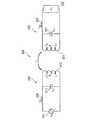
図1は、本発明の第1実施形態に係る非接触給電システムの回路図である。非接触給電システム100は、送電装置101と受電装置103とを備えている。送電装置101は、後述の送電コイル113を含み、受電装置103は、後述の受電コイル121を含む。送電装置101は、コイル間の磁気結合により、受電装置103に非接触で電力を伝送する。コイル間の磁気結合を利用して電力を伝送する方式は、例えば、電磁誘導方式や磁界共鳴方式である。非接触給電システム100の適用例としては、例えば、電気自動車(車両)や水中航走体等の移動体、家電製品又は医療機器の、充電システムや駆動システムである。送電コイル113と受電コイル121は、たとえばソレノイド型やサーキュラー型のコイルである。なお、ソレノイド型とは、コイルを形成する導線が三次元空間的に螺旋状に巻回された態様である。サーキュラー型とは、コイルを形成する導線が平面渦巻状に巻回された態様である。(First embodiment)
FIG. 1 is a circuit diagram of a contactless power feeding system according to a first embodiment of the present invention. The non-contact
送電装置101は、ある周波数fの交流電力を出力する電源111から交流電力が入力される送電コイル113と、虚数インピーダンスを有する素子(送電側直列素子)115とを含んでいる。すなわち、送電コイル113は、電源111からある周波数fの交流電力を受けるように構成されている。ある周波数fの交流電力とは、電源111から出力される交流電圧又は交流電流の周波数がfであることを意味する。素子115は、電源111と送電コイル113とに直列に接続されている。送電コイル113の自己インダクタンスをL1で示し、送電コイル113には、電流I1(フェーザ電流)が流れる。なお、フェーザ表示された電流の絶対値は、実効値であっても波高値であってもよい。The
電源111は、例えば、インバータ回路のような電源回路や商用電源のような交流(AC)電源であり、周波数f(角周波数ω)の交流電圧VS(フェーザ電圧)を出力する。電源111により供給された交流電力は、素子115を介して送電コイル113によって受けられる。インバータ回路は、ハーフブリッジ方式やフルブリッジ方式等の従来公知の方式で実現され得る。なお、フェーザ表示された電圧の絶対値は、実効値であっても波高値であってもよい。The
電源111がインバータ回路で構成されている場合、インバータ回路は、複数のスイッチング素子(電界効果トランジスタ等)を含み、これらの素子がスイッチング周波数fでスイッチングされることにより、周波数fの交流電力が電源111から出力される。つまり、インバータ回路出力の周波数を変更するために、スイッチング周波数が制御される。なお、インバータ回路の方式によってはインバータ回路から出力される交流の周波数がスイッチング周波数に一致しないこともある。また、インバータ回路には、直流電力が入力されるが、この直流電力は、例えば、直流(DC)電源から供給された電力であったり、電力変換回路によって交流電力が直流電力に変換された電力であったりする。電力変換回路は、例えば、整流機能を含み、選択的にPFC(Power Factor Correction:力率改善)機能や電圧変換機能を有する。電圧変換機能は、例えば、チョッパ回路を用いた非絶縁型のDC−DCコンバータや、トランス等を用いた絶縁型のDC−DCコンバータで実現される。 In the case where the
素子115は、例えば、インダクタ(リアクトル、コイル)やキャパシタ等のリアクタンス素子、又はそれらの組合せの複数の素子により構成され、素子115の虚数インピーダンスをjZS1i(j:虚数単位、ZS1i:虚部)で示す。以下、虚部は実数である。素子115が複数の素子で構成される場合、例えば、電源111の一方の端子とコイル113との間(図1の電源111とコイル113との間の一方の接続線)に1つ素子を設け、電源111の他方の端子とコイル113との間(図1の電源111とコイル113との間の他方の接続線)に1つ素子を設けることができる。この場合、素子115のインピーダンスは、これら2つの素子の合成インピーダンスとなる。素子がキャパシタである場合、素子115のインピーダンスを複数のキャパシタで実現することにより、各キャパシタに印加される電圧を小さくすることができる。よって、耐電圧の低いキャパシタを採用することができ、送電装置101の小型化が可能となる。The
受電装置103は、ある結合係数kで送電コイル113と磁気結合するように構成された受電コイル121と、虚数インピーダンスを有する素子(受電側直列素子)123とを含んでいる。素子123は、受電コイル121に直列に接続されている。また、素子123には、実数インピーダンスを有する負荷125が直列に接続されている。受電コイル121の自己インダクタンスをL2で示し、受電コイル121には、電流I2(フェーザ電流)が流れる。The
送電コイル113と受電コイル121との間の位置ずれによる結合係数kの変動範囲が予め定められている場合がある。例えば、位置ずれにより、送電コイル113と受電コイル121との間の結合係数が小さくなると、電力効率は下がる。そのため、所望の電力効率を実現するという観点から、許容される最低の電力効率を実現する結合係数kの下限値kminが存在する。所望の結合係数kの上限値kmaxは、非接触給電システム100として実現可能な最大値となる。また、非接触給電システム100の位置ずれ範囲が予め定められているような場合には、この範囲内の非接触給電システム100の結合係数kを求めることにより、結合係数kの変動範囲が定められる。また、変動範囲とは、非接触給電システム100の正常動作が保証される使用許可範囲であってもよい。この使用許可範囲は、例えば、仕様書もしくは使用マニュアル等に記載される。There may be a case where a fluctuation range of the coupling coefficient k due to a positional shift between the
送電コイル113及び受電コイル121の自己インダクタンスは、結合係数kに応じて変わり得る。この場合、結合係数の変動範囲内での変化に応じて、自己インダクタンスの変化範囲が存在する。そこで、送電コイル113及び受電コイル121の自己インダクタンスを、変化範囲内のいずれかの値に設定してもよい。また、自己インダクタンスを、変化範囲内の値の平均値に設定してもよい。 The self-inductances of the
素子123は、インダクタ(リアクトル、コイル)やキャパシタ等のリアクタンス素子、又はそれらの組合せの複数の素子により構成される構成要素であり、素子123の虚数インピーダンスをjZS2iで示す。負荷125は、例えば、電力を蓄積する蓄電デバイス(リチウムイオン二次電池やニッケル水素二次電池、大容量の電気二重層キャパシタ等)や電力で駆動される電気機器・電子機器であり、負荷125の実数インピーダンスをZ2rで示す。なお、素子123が複数の素子で構成される場合、これらの素子の合成インピーダンスは、虚数インピーダンスと実数インピーダンスとで構成される場合がある。この場合、合成インピーダンスの虚数インピーダンスがjZS2iとなり、合成インピーダンスの実数インピーダンスと負荷125の実数インピーダンスとの合成がZ2rとなる。また、リアクタンス素子や二次電池以外に電力変換回路が受電コイル121に接続されている場合には、リアクタンス素子と、二次電池と、電力変換回路との合成インピーダンスの実部が負荷125の実数インピーダンスZ2rを構成し、虚部が素子123の虚数インピーダンスZS2iを構成する。なお、電力変換回路とは、整流回路や、整流回路とDC−DCコンバータとの組合せ等の種々の回路により構成できる。The
送電コイル113と受電コイル121との相互インダクタンスMは、M2=k2L1L2の関係式を満たすので、図1の回路方程式は、式(10)になる。Since the mutual inductance M between the
式(10)から、電流I1とI2の関係式を求めると、式(11)になる。When a relational expression between the currents I1 and I2 is obtained from Expression (10), Expression (11) is obtained.
式(12)が成立する場合、式(11)及び式(12)より、式(13)が成立する。 When Expression (12) is satisfied, Expression (13) is satisfied from Expression (11) and Expression (12).
次に、式(10)及び式(11)を用いて、送電コイル113から受電側を見たインピーダンスZ1(送電コイル113を含むインピーダンス)を求めると、インピーダンスZ1は式(14)で示される。なお、式(14)中のV1は、送電コイルに印加される電圧を示す。また、「ある構成要素から受電側を見たインピーダンス」との記述は、非接触給電システムの送電側を上流側とし、非接触給電システムの受電側を下流側とした場合に、「この構成要素から下流側のインピーダンス」を意味する(以下同様)。Next, when using equation (10) and equation (11) to determine the impedance Z1 (impedance including the power transmission coil 113) as seen from the
ここで、式(12)が成立するように非接触給電システム100の各パラメータ(素子のインピーダンス、周波数、結合係数)が決定又は制御される。この場合、式(13)を式(14)に代入することにより、式(14)は、式(15)になる。 Here, each parameter (element impedance, frequency, coupling coefficient) of the non-contact
よって、電源111から受電側を見たインピーダンスZS(電源111を含まないインピーダンス)は、式(16)で示される。Therefore, the impedance ZS (impedance not including the power supply 111) when the power reception side is viewed from the
式(16)より、電源111から受電側を見たインピーダンスZSは、受電側の負荷125の実数インピーダンスZ2rと、素子115及び123の虚数インピーダンスjZS1i及びjZS2iとで表現され、結合係数kを含まない。実数インピーダンスZ2rと虚数インピーダンスjZS1i及びjZS2iとは、結合係数kに非依存であるため、インピーダンスZSも結合係数kに非依存となる。つまり、結合係数が変化しても、式(12)が成立するように周波数fが選択されれば(定められれば)、インピーダンスZS、ひいては交流電圧VS(=ZS/I1)は、変動しなくなる。式(12)が成立するとは、周波数f、結合係数k、素子123の虚数インピーダンスZS2iの組合せが、式(13)を満たすことである。つまり、式(12)が成立するかは、送電装置101の素子のインピーダンスと関係がない。また、インピーダンスZSの実部は、負荷125のインピーダンスと送電コイル113及び受電コイル121の自己インダクタンスのみで表現され、素子115、123のインピーダンスの影響を受けない。From equation (16), the impedance ZS when the power receiving side is viewed from the
結合係数kが変化する状況としては、例えば、送電コイル113と受電コイル121との相対位置関係(図2における車両Vの進行方向である前後方向及び車両Vの回転方向(旋回方向)である左右方向に関する位置関係)が変わると、結合係数kが変わる。また、送電コイル113と受電コイル121との間隔D(図2における高さ方向におけるギャップ距離)が変わっても、結合係数kが変わる。更に、送電コイル113に対する受電コイル121の向き又は傾きが変わっても、結合係数kが変わる。この場合、変化後の結合係数で式(13)が成立するように周波数を選ぶことにより、インピーダンスZSが変化後の結合係数の影響を受けなくなり、交流電圧VSの変動を抑えることができる。以下、上記3つの方向(前後方向、左右方向、高さ方向)の少なくとも1方向において、送電コイル113又は受電コイル121が所望の位置からずれたり、送電コイル113に対する受電コイル121の向き又は傾きが所望の向き又は傾きからずれたりすることを位置ずれと表現する。As a situation where the coupling coefficient k changes, for example, the relative positional relationship between the
なお、式(12)が成立するとの意味は、厳密に式(12)における等号関係が成立することに限定されない。例えば、測定誤差若しくは制御誤差、又は予め規定されるVSの許容変動範囲等に基づき、誤差範囲を予め定め、I1とI2の比と、L2とL1の比の平方根との差分が、その誤差範囲に含まれていれば、式(12)は成立しているとみなすことができる。または、上記差分が誤差範囲に含まれていれば、インピーダンスZSは、結合係数kに非依存であるとみなせる。また、送電コイル113及び受電コイル121のインダクタンスL1とL2は、送受電コイル間の相対位置関係により変わる場合がある。そのため、給電前に予め測定した初期値L1及びL2と、給電中の実際値L1r及びL2rとの間にズレが生じる。そのため、式(12)の関係式が満たされるように、初期値L1及びL2を用いて非接触給電システムが設計されると、給電中の実際値L1r及びL2rとコイル電流との関係においては、式(17)のように誤差εが発生する。なお、送電コイル113及び受電コイル121のインダクタンスL1とL2の変化を取り上げているが、素子123のインピーダンスjZS2iが変わった場合にも、電流I1及びI2が変化する場合があり、よって式(17)が成立する。In addition, the meaning that Formula (12) is materialized is not limited to the exact equality relationship in Formula (12) being materialized. For example, the measurement error or the control error, or based on pre-defined allowable variation range of the VS or the like, a predetermined error range, the difference between the ratio of I1 and I2, and the square root of the ratio of L2 and L1 However, if it is included in the error range, it can be considered that Formula (12) is materialized. Alternatively, if the difference is included in the error range, the impedance ZS can be regarded as independent of the coupling coefficient k. Further, the inductance L1 and L2 of the transmitting
この場合、給電中の実際値において、送電コイル113から受電側を見たインピーダンスZ1は、式(18)で表現され、電源111から受電側を見たインピーダンスZSは、式(19)で表現される。式(19)より、誤差εが発生しても、インピーダンスZSは結合係数kに非依存である。In this case, in the actual value during power feeding, the impedance Z1 when the power receiving side is viewed from the
インピーダンスZSが結合係数kに非依存となり、電源111からの交流電圧VSが変動しにくくなるということは、交流電圧VSと相関関係のある送電側の電圧(例えば、送電コイル113の両端間の電圧V1)も変動しにくくなる。また、電源111がインバータ回路で構成されている場合、インバータ回路の入力直流電圧と出力交流電圧とは、連動するため、出力交流電圧VSが変動しにくくなるということは、入力直流電圧も変動しにくくなる。この直流電圧を出力する電力変換回路がチョッパ回路を有する場合、電力変換回路の出力端にキャパシタが設けられるが、電力変換回路からの直流電圧の変動が抑えられることにより、このキャパシタの耐電圧を小さくできる。そのため、キャパシタの小型化、ひいては送電装置101の小型化が可能になる。The impedance ZS becomes independent of the coupling coefficient k, and the AC voltage VS from the
更に、式(16)において、虚数インピーダンスZS1iが式(20)を満たすときには、式(16)の虚部が打ち消され、式(21)のようにインピーダンスZSは実部のみを有する。このとき、電源111の力率は100%となる。一方、虚数インピーダンスZS1iの値を式(20)の値からずらすことにより、インピーダンスZSが結合係数kに依存することなく、力率を所望の値にすることができる。Furthermore, in the equation (16), when the imaginary impedance ZS1i satisfies the equation (20), the imaginary part of the equation (16) is canceled, and the impedance ZS has only a real part as in the equation (21). At this time, the power factor of the
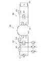
続いて、コイル間の結合係数が変化した場合にどのように周波数を変更するかの具体的制御手法について図3を用いて説明する。図3は、本発明の第1実施形態に係る非接触給電システムの機能ブロック図である。 Next, a specific control method for changing the frequency when the coupling coefficient between the coils changes will be described with reference to FIG. FIG. 3 is a functional block diagram of the non-contact power feeding system according to the first embodiment of the present invention.
まず、送電装置101の機能ブロックについて説明する。送電装置101は、交流電力出力部141と、送電部143と、送電側検出部145と、送電側通信部147と、記憶部148と、送電側制御部149とを備えている。交流電力出力部141は、送電部143に接続され、送電部143は、送電側検出部145に接続され、送電側制御部149は、交流電力出力部141、送電側検出部145、送電側通信部147及び記憶部148にそれぞれ接続されている。なお、交流電力出力部141は、送電装置101の外部に設けることもできる。また、各機能ブロックの機能は、ハードウェアにより実現される。具体的には、送電部143の機能は送電器により、送電側検出部145の機能は送電側検出器により、送電側通信部147の機能は送電側通信機により、記憶部148の機能はメモリにより、送電側制御部149の機能は送電側制御器により、それぞれ実現され得る。 First, functional blocks of the
交流電力出力部141は、図1の電源111に相当し、交流電力を出力する。また、送電部143は、図1の送電コイル113と素子115とに相当し、受電装置103の後述の受電部151に対して電力を送る。 The AC
送電側検出部145は、送電部143の送電状況を示す値として、送電コイル113に流れる電流I1を検出する電流センサであり、検出した電流データを送電側制御部149に送る。電流センサとしては、たとえば、電流の通過する電線の周囲に発生する磁界をホール効果により測定するセンサや、電流の通過する電線に抵抗を挿入しこの抵抗で生じる電位降下を測定するセンサが使用可能である。The power transmission
送電側通信部147は、後述の受電側通信部155と無線通信を行う。送電側通信部147と受電側通信部155との通信方式は、例えば、ZigBee(登録商標)やBluetooth(登録商標)等の電波を用いた無線通信あるいは光信号を用いた光通信である。電波を用いた通信方式の場合、送電側通信部147はアンテナを有し、光信号を用いた通信方式の場合、送電側通信部147は通信用の発光素子や受光素子を有する。 The power transmission
記憶部148は、結合係数に関する情報や素子のインピーダンス(L1、L2等の値)等の各種情報や、後述の送電側制御部149の各機能を記述するプログラム等を記憶し、RAM(Random Access Memory)等の揮発性の記憶媒体や、ROM(Read Only Memory)等の不揮発性の記憶媒体で構成される。結合係数に関する情報とは、例えば、送電コイル113と受電コイル121との結合係数を特定するために必要な情報や、式(12)を満たすときの結合係数kと周波数fとの組合せの情報である。The
送電側制御部149は、送電装置101の各機能ブロック、及び送電装置101の全体を制御及び管理している。送電側制御部149は、例えば、CPU(中央処理装置)等の任意の好適なプロセッサや、処理ごとに特化した専用のプロセッサ(例えばDSP(デジタルシグナルプロセッサ))によって構成される。送電側制御部149が行う具体的処理については、後述する。 The power transmission
次に、受電装置103の機能ブロックについて説明する。受電装置103は、受電部151と、受電側検出部153と、受電側通信部155と、受電側制御部157とを備えている。受電部151は、受電側検出部153に接続され、受電側検出部153及び受電側通信部155は、受電側制御部157にそれぞれ接続されている。また、各機能ブロックの機能は、ハードウェアにより実現される。具体的には、受電部151の機能は受電器により、受電側検出部153の機能は受電側検出器により、受電側通信部155の機能は受電側通信機により、受電側制御部157の機能は受電側制御器により、それぞれ実現され得る。なお、受電装置103も、送電装置101と同様、受電側制御部157の各機能を記述するプログラム等を記憶する記憶部を有しているが、図示は省略する。 Next, functional blocks of the
受電部151は、図1の受電コイル121と素子123とに相当し、送電部143から送信された電力を受け取り、その電力を負荷125に供給する。 The
受電側検出部153は、受電部151の受電状況を示す値として、受電コイル121に流れる電流I2を検出する電流センサであり、検出した電流データを受電側制御部157に送る。電流センサとしては、たとえば、電流の通過する電線の周囲に発生する磁界をホール効果により測定するセンサや、電流の通過する電線に抵抗を挿入しこの抵抗で生じる電位降下を測定するセンサが使用可能である。The power reception
受電側通信部155は、送電側通信部147と無線通信を行う。電波を用いた通信方式の場合、受電側通信部155はアンテナを有し、光信号を用いた通信方式の場合、受電側通信部155は通信用の発光素子や受光素子を有する。 The power reception
受電側制御部157は、受電装置103の各機能ブロック、及び受電装置103の全体を制御及び管理している。受電側制御部157は、例えば、CPUやDSP等の任意のプロセッサによって構成される。受電側制御部157が行う具体的処理については、後述する。 The power receiving
続いて、位置ずれにより結合係数が変化した場合の送電側制御部149及び受電側制御部157の具体的制御内容を説明する。以下、位置ずれがない場合の結合係数をk1で示し、そのときに式(12)を満たす周波数をf1で示し、記憶部148がこれらの値を対応付けて記憶している。Next, specific control contents of the power transmission
送電側制御部149は、位置ずれが生じていないと仮定し、位置ずれ無しに相当する周波数f1の交流電力を出力するように交流電力出力部141を制御する。送電部143がこの交流電力を受電部151に送る。また、送電側検出部145は、送電コイル113に流れる電流I1を検出し、そのデータを送電側制御部149に送る。一方、受電側検出部153は、受電コイル121に流れる電流I2を検出して、そのデータを受電側制御部157に送る。受電側制御部157は、受け取った電流データを送電装置101に送信するように受電側通信部155を制御する。The power transmission
すると、送電側通信部147が、受電側通信部155から電流データを受信し、送電側制御部149に送る。送電側制御部149は、記憶部148に記憶されているL1及びL2の値を読み出し、読み出されたL1及びL2の値及び受け取ったI1、I2のデータから、式(12)が成立しているかを判断する。Then, the power transmission
式(12)が成立している場合には、送電側制御部149は、送電コイル113と受電コイル121とは、所望の位置関係にあり、位置ずれはないと判断する。そして、送電側制御部149は、周波数を変更せずに、周波数f1の交流電力を出力し続けるように交流電力出力部141を制御する。When Expression (12) is established, the power transmission
式(12)が成立していない場合には、送電側制御部149は、送電コイル113と受電コイル121との相対的位置関係が所望の位置からずれていると判断する。位置ずれにより、コイル113及び121に流れる電流が変化するため、送電側制御部149は、検出値であるI1及びI2と、記憶値であるL1及びL2とから、電流の変化量α(αは1より大もしくは小な値)を算出する(式(22)参照)。When Expression (12) is not established, the power transmission
式(11)の右辺において、素子及び負荷のインピーダンスが一定である場合、位置ずれが原因で変化するパラメータは結合係数のみである。つまり、この変化量αは、結合係数の変化量に対応するため、位置ずれ後の結合係数k2は、式(23)で示される値となる。
k2=αk1 式(23)On the right side of Equation (11), when the impedances of the element and the load are constant, the only parameter that changes due to misalignment is the coupling coefficient. That is, since the change amount α corresponds to the change amount of the coupling coefficient, the coupling coefficient k2 after the positional deviation is a value represented by the equation (23).
k2 = αk1 formula (23)
よって、送電側制御部149は、記憶部148に記憶されている結合係数k1の値を読み出し、式(23)を用いて位置ずれ後の結合係数k2を求め、結合係数k2のときに式(12)を満足する周波数f2を、式(13)より算出する。送電側制御部149は、この周波数f2の交流電力を出力するよう交流電力出力部141を制御する。Therefore, the power-transmitting-
以上に示すように、周波数変更の具体的制御手法の一例を説明したが、以下では、その変形例として、送電側検出部145を使用せずに周波数を変更する方法を述べる。この場合の機能ブロック図としては、送電側検出部145がなくなる以外は、図3と同じである。以下、上記の説明と異なるところを中心に説明する。機能ブロック141、143、147、151、155の機能は、上記の説明と同じであるため、重複する説明は省略する。 As described above, an example of a specific control method for changing the frequency has been described. Hereinafter, a method for changing the frequency without using the power transmission
記憶部148は、結合係数に関する情報として、受電装置103における受電電力と結合係数との関係を記憶する。この関係は、例えば、交流電力出力部141が所定周波数(結合係数を求める際には周波数を固定するため)で一定電力を出力しているときの、負荷125に供給される電力(供給電力)と結合係数との関係である。なお、以下、記憶部148に記憶される結合係数に関する情報は、受電電力と結合係数との関係であるが、この態様に限定されるものではない。結合係数に関する情報として、結合係数と相関関係のあるパラメータを任意に利用することができる。結合係数と相関関係のあるパラメータとは、例えば、受電コイル121の電流I2である。The
受電側検出部153は、負荷125に印加される電圧及び負荷125へ入力される電流を受電状況として検出する電圧センサ及び電流センサである。なお、検出箇所は、負荷125に限定されるものではなく、受電側検出部153は、素子123に関する電圧・電流を測定してもよい。また、検出対象は、電圧・電流に限定されず、電力でもよく、この場合、受電側検出部153は電力センサである。電圧センサとしては、たとえば、抵抗により電圧を分圧しADコンバータで電圧をデジタル値に変換するセンサがある。また、電力センサとしては、たとえば、電圧センサと電流センサにより電圧と電流を計測し、これらの電圧と電流を乗じた値を時間的に平均化して電力を求めるセンサがある。 The power receiving
送電装置101が、周波数f1の交流電力を出力すると、受電部151がこの電力を受け取り、受電側検出部153は、負荷125に関する電圧及び電流を検出して、そのデータを受電側制御部157に送る。受電側制御部157は、受け取ったデータから負荷125で充電(消費)されている電力値を算出する。そして、受電側制御部157は、この電力値データを送電装置101に送信するように受電側通信部155を制御する。When the
送電側通信部147は、受電側通信部155から電力値データを受信する。送電側制御部149は、記憶部148に記憶されている受電電力と結合係数との関係を読み出し、読み出された結合係数k1に対応する電力値と、受け取った電力値データとが一致するかを判断する。なお、一致するとは、厳密に等式が成り立つことに限定されるものではなく、送電側制御部149は、読み出した電力値と受け取った電力値との差分が予め定められた誤差範囲内であれば一致するとみなすこともできる。The power transmission
一致している場合には、送電側制御部149は、送電コイル113と受電コイル121とは、所望の位置関係にあり、位置ずれはないと判断する。そして、送電側制御部149は、周波数を変更せずに、周波数f1の交流電力を出力し続けるように交流電力出力部141を制御する。If they match, the power transmission
一致していない場合には、送電側制御部149は、送電コイル113と受電コイル121との相対的位置関係が所望の位置からずれていると判断し、記憶部148に記憶されている関係(例えば受電電力と結合係数との関係)から、受け取った電力値データに対応する結合係数k2を特定する。そして、送電側制御部149は、結合係数k2のときに式(12)を満足する周波数f2を算出し、この周波数f2の交流電力を出力するよう交流電力出力部141を制御する。If they do not match, the power transmission
このように本実施形態の非接触給電システム100では、結合係数kが変化した場合に、周波数f及び素子123の虚数インピーダンスjZS2iは、式(12)を満たすことに基づいて、電源111から受電側を見たときのインピーダンスZSが結合係数kに非依存となるように定められている。つまり、本実施形態では、非接触給電システム100が式(12)を満足することにより、インピーダンスZSは、負荷125の実数インピーダンスZ2rと虚数インピーダンスjZS1i及びjZS2iとで表現され、結合係数kに非依存となる。そのため、送電コイル113と受電コイル121との位置ずれやコイル間距離の変化により、結合係数kが変化した場合に、送電側制御部149は、周波数fを式(12)が成立するように選択する。すなわち、送電側制御部149は、以下を行うように構成されている。送電側制御部149は、結合係数kが変化した場合に、電源111から受電側を見たときのインピーダンスZSが結合係数kに非依存となるように、周波数fを調節する。このように周波数fを変化させた場合に、結合係数kの変化に因ってインピーダンスZSが変わることはないため、インピーダンスZSの変動を抑えることができる。そして、インピーダンスZSが変動し難い分、交流電圧VSの変動を抑えることが可能になる。As described above, in the non-contact
また、本実施形態では、送電装置101の素子115と、受電装置103の素子123とは、式(20)を満たすように設定できる。この場合、インピーダンスZSは虚部を有さなくなり、電源111から受電側を見たインピーダンスZSが結合係数非依存になるだけでなく、電源111の力率が100%になる。よって、電源111での送電効率を最大化できる。また、このとき、受電側から送電側を見たインピーダンスも純抵抗(インダクタンス及びキャパシタンスをいずれも含まない抵抗)になるため、電源111から負荷125への送電効率と同じ効率で負荷125から電源111へ電力を伝送することができる。つまり、双方向電力伝送を実施できる。In the present embodiment, the
また、本実施形態のように、式(12)が成立するように非接触給電システム100を設計することは、複数の受電装置の間、又は複数の送電装置の間における相互互換性を確保する場合に利点がある。例えば、式(12)が成立する送電装置101と受電装置103を設計し、さらに負荷125とは異なるインピーダンスZ2raの負荷(第2負荷)へ給電するための受電装置(第2受電装置)の設計が必要になった場合を説明する(なお、第2受電装置の回路構成は、受電装置103と同じであり、第2受電装置の素子のインピーダンスのみが受電装置103と異なる)。この場合、β=Z2ra/Z2rを求め、第2受電装置の受電コイル(第2受電コイル:受電コイル121に対応)の自己インダクタンスL2a及び素子(第2素子:素子123に対応)の虚数インピーダンスjZS2iaを式(24)及び式(25)を満たすように定める。
L2a=βL2 式(24)
ZS2ia=βZS2i式(25)
このとき、送電装置101と第2受電装置とが組み合わされると、電源111から受電側を見たインピーダンスZSは式(16)で示される値になる。つまり、式(24)及び式(25)が成立するように第2受電装置を実現することにより、送電装置101を変更しなくても、電源111から受電側を見たインピーダンスを一定にすることができる。これにより、負荷のインピーダンスが変化しても、簡易な設計変更により、送電側の電圧が変動し難い非接触給電システムを構築することができる。In addition, as in the present embodiment, designing the non-contact
L2a = βL2 formula (24)
ZS2ia = βZS2i Formula (25)
At this time, when the
同様にして、負荷125に、電源111と異なる電圧VSaを出力する電源(第2電源)から、電源111の場合と同じ電力を供給する必要が生じた場合にも、簡易な設計変更により、電圧VSaが供給される送電装置(以下、第2送電装置)を構成することができる(なお、第2送電装置の回路構成は、送電装置101と同じであり、第2送電装置の素子のインピーダンスのみが送電装置101と異なる)。具体的には、第2電源が、電源111と同じ電力Pを出力するためには、第2電源から受電側を見たインピーダンスZSaが式(26)を満たす必要がある。Similarly, when it is necessary to supply the same power as that of the
γ=(VSa/VS)2とすると、第2送電装置の送電コイル(第2送電コイル:送電コイル113に対応)の自己インダクタンスL1a及び素子(第3素子:素子115に対応)の虚数インピーダンスjZS1iaが式(27)及び式(28)を満たすことにより、式(26)は満たされる。
L1a=γL1 式(27)
ZS1ia=γZS1i式(28)
つまり、式(27)及び式(28)が成立するように第2送電装置を実現することにより、受電装置103を変更しなくても、負荷125には一定電圧を供給することができる。これにより、電源の電圧が変化しても、簡易な設計変更により、送電側の電圧が変動し難い非接触給電システムを構築することができる。When γ = (VSa / VS )2 , the self-inductance L1a of the power transmission coil (second power transmission coil: corresponding to the power transmission coil 113) and the element (third element: corresponding to the element 115) of the second power transmission device When the imaginary impedance jZS1ia satisfies Expression (27) and Expression (28), Expression (26) is satisfied.
L1a = γL Formula1 (27)
ZS1ia = γZS1i Formula (28)
That is, by realizing the second power transmission device so that Equation (27) and Equation (28) are satisfied, a constant voltage can be supplied to the
(第2実施形態)
第1実施形態では、虚数インピーダンスを有する素子115が送電コイル113に直列に接続されると共に、虚数インピーダンスを有する素子123が受電コイル121に直列に接続されている場合について説明したが、第2実施形態では、送電コイル及び受電コイルのそれぞれに並列にも虚数インピーダンスを有する素子が接続されている場合について説明する。(Second Embodiment)
In the first embodiment, the case where the
第2実施形態に係る非接触給電システム200は、送電装置201と、受電装置203とを備えている。送電装置201は、電源211から交流電力が入力される送電コイル213と、素子(送電側直列素子)215と、素子(送電側並列素子)217とを含んでいる。受電装置203は、受電コイル221と、素子(受電側直列素子)223と、素子(受電側並列素子)227とを含んでいる。素子223には、負荷225が直列に接続されている。これらの構成要素211、213、215、221、223、225は、第1実施形態の送電装置101及び受電装置103の構成要素111、113、115、121、123、125とそれぞれ同一であるため、重複する説明は省略する。以下、図4の回路において、電源211から受電側を見たインピーダンスZS(電源211を含まないインピーダンス)が結合係数に非依存となることを示す。なお、非接触給電システム200は、図5に示すように、交流電力出力部241、送電部243、送電側検出部245、送電側通信部247、記憶部248、送電側制御部249、受電部251、受電側検出部253、受電側通信部255及び受電側制御部257を備え、各機能部の機能は、それぞれ対応する第1実施形態の機能部の機能と同一であるため、重複する説明は省略する。また、周波数の変更制御方法についても、第1実施形態と同じ方法を利用できる。A non-contact
素子217は、送電コイル213に並列に接続され、且つ素子215よりも送電コイル側に接続され、虚数インピーダンスjZP1iを有している。すなわち、素子217は、素子215よりも送電コイル213に近い位置で送電コイル213に並列に接続され、虚数インピーダンスjZP1iを有している。この接続関係を言い換えると、素子215は、送電コイル213に直列に接続され、且つ素子217よりも電源211に近い位置に接続されている。また、素子227は、受電コイル221に並列に接続され、且つ素子223よりも受電コイル側に接続され、虚数インピーダンスjZP2iを有している。すなわち、素子227は、素子223よりも受電コイル221に近い位置で受電コイル221に並列に接続され、虚数インピーダンスjZP2iを有している。素子217及び227は、例えば、インダクタ(リアクトル、コイル)やキャパシタ等のリアクタンス素子、又はそれらの組合せの複数の素子により構成される。The
図4の回路方程式を立てると、式(29)になる。 When the circuit equation of FIG. 4 is established, Equation (29) is obtained.
第1実施形態のように、式(12)が成立するように非接触給電システム200の各パラメータが決定又は制御される。この場合、素子217から受電側を見たインピーダンスZ1(素子217を含むインピーダンス)を求めると式(30)で示される値になり、この式は結合係数kを含まない。As in the first embodiment, each parameter of the non-contact
式(31)が成立するように送電側並列素子217及び受電側並列素子227のインピーダンスの値が決定されていると、式(30)及び式(31)より、式(32)が成立する。 When the impedance values of the power transmission side
よって、電源211から受電側を見たインピーダンスZSは、式(33)で示される値になる。Therefore, the impedance ZS when the power receiving side is viewed from the
式(33)によれば、式(12)及び式(31)が成立している場合には、電源211から受電側を見たインピーダンスZSは、受電側の負荷225の実数インピーダンスZ2rと、素子215及び223の虚数インピーダンスjZS1i及びjZS2iとで表現される。負荷225の実数インピーダンスZ2rと虚数インピーダンスjZS1i及びjZS2iとは、結合係数kに非依存であるため、インピーダンスZSも結合係数kに非依存となる。また、インピーダンスZSの実部は、負荷225のインピーダンスと送電コイル213及び受電コイル221の自己インダクタンスのみで表現され、素子215、217、223、227のインピーダンスの影響を受けない。According to the equation (33), when the equations (12) and (31) are established, the impedance ZS viewed from the
更に、虚数インピーダンスZS1iが式(34)を満たすときには、式(33)の虚部が打ち消され、式(35)のようにインピーダンスZSは実部のみを有する。このとき、電源211の力率は100%となる。一方、虚数インピーダンスZS1iの値を式(34)の値からずらすことにより、インピーダンスZSが結合係数kに依存することなく、力率を所望の値にすることができる。Further, when the imaginary impedance ZS1i satisfies the equation (34), the imaginary part of the equation (33) is canceled, and the impedance ZS has only the real part as in the equation (35). At this time, the power factor of the
図4の回路がより具体的な回路素子で構成されている場合について説明する。具体的には、図6のように素子215及び223をインダクタ(自己インダクタンス:LS1及びLS2)で構成し、素子217及び227をキャパシタ(キャパシタンス:CP1及びCP2)で構成する。A case where the circuit of FIG. 4 is configured with more specific circuit elements will be described. Specifically, as shown in FIG. 6, the
このとき、素子217及び227のキャパシタンスの関係は、式(31)より、式(36)で示される。式(12)及び式(36)が成立している場合、電源211から受電側を見たインピーダンスZSの実部は、結合係数kに非依存となる。At this time, the relationship between the capacitances of the
また、素子215及び223の自己インダクタンスの関係は、式(34)より、式(37)で示される。式(12)、式(36)及び式(37)が成立している場合、電源211の力率は100%となる。 Further, the relationship between the self-inductances of the
図6の回路構成において、式(12)を満たす結合係数kと周波数fの関係について説明する。図6の回路方程式から電流I1に対する電流I2の割合を求めると、その割合は式(38)で示される値になる。In the circuit configuration of FIG. 6, the relationship between the coupling coefficient k and the frequency f satisfying Expression (12) will be described. When the ratio of the current I2 to the current I1 is obtained from the circuit equation of FIG. 6, the ratio is a value represented by the equation (38).
式(38)が式(12)を満たす場合、式(39)が成立する。なお、式(39)中のアスタリスク「*」は、複素共役を示している。 When Expression (38) satisfies Expression (12), Expression (39) is established. Note that an asterisk “*” in formula (39) indicates a complex conjugate.
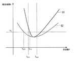
素子及び負荷のインピーダンスが固定である場合、結合係数kは、角周波数ω(つまり周波数f)の関数となり、この関数は図7の実線のグラフG1で示される。なお、比較対象である図7の破線のグラフG2は、受電装置203の素子223をインダクタではなく、キャパシタのみで構成した場合の結果を示している。素子223をキャパシタのみで構成するよりも素子223をインダクタで構成するほうが、グラフの傾きの大きさがより大きい結果が得られ、つまり周波数fを変化させた場合に式(12)を満たす結合係数kの変化幅が大きくなる。 When the impedance of the element and the load is fixed, the coupling coefficient k becomes a function of the angular frequency ω (that is, the frequency f), and this function is shown by a solid line graph G1 in FIG. Note that a broken-line graph G2 in FIG. 7 as a comparison target shows a result in a case where the
例えば、電源211や非接触給電システム200全体の制約として、周波数fの可変範囲(fmin(下限値)≦f≦fmax(上限値))が定められ、この可変範囲が、グラフG1及びG2に対して、図7のように定められている場合を説明する。可変範囲は、例えば、電源211が出力可能な電力の周波数範囲の上下限で定められる。送電コイルと受電コイルとの間の位置ずれ等により結合係数が図7のk3で示される値になった場合、グラフG1では、式(12)を満たす周波数f3−1は、可変範囲内に含まれる。一方、グラフG2では、式(12)を満たす周波数f3−2は、可変範囲の外にある。つまり、受電装置203の受電側直列素子223をインダクタで構成すると、キャパシタで構成する場合に比べ、結合係数が大きく変化しても、式(12)を満たす周波数が可変範囲内に存在する可能性が高くなる。これにより、より広い範囲での結合係数の変化に対して、電源211からの交流電圧の変動を抑えつつ周波数を変更することができる。For example, a variable range (fmin (lower limit value) ≦ f ≦ fmax (upper limit value)) of the frequency f is determined as a restriction on the
また、素子223(インダクタ)の自己インダクタンスLS2又は素子227(キャパシタ)のキャパシタンスCP2の少なくとも一方を任意の値に設定できる場合、設定値の変化に合わせて、グラフG1の形が変化する。例えば、可変範囲で結合係数が単調減少又は単調増加となるように、自己インダクタンスLS2の値を選択すれば、結合係数の極小値が可変範囲の中に位置する場合に比べ、結合係数kの変化幅が大きくなる。特に、式(12)を満たす結合係数kと周波数fとの関係が、図8のように結合係数の極小値を中心に非対称(この極小値を通り図8の結合係数の軸(上下軸)に平行な線に関して非対称)である場合には、より傾きの絶対値が大きい領域(図8では、単調減少の領域、極小値の左側)に周波数fの可変範囲が位置することが好ましい。Further, when at least one of the capacitance CP2 of self-inductance LS2 or element 227 (capacitor) element 223 (inductor) may be set to an arbitrary value, in accordance with the change in the set value, the form of the graph G1 is changed. For example, if the value of the self-inductance LS2 is selected so that the coupling coefficient monotonously decreases or monotonically increases in the variable range, the coupling coefficient k is smaller than when the minimum value of the coupling coefficient is located in the variable range. The range of change becomes large. In particular, the relationship between the coupling coefficient k and the frequency f satisfying the equation (12) is asymmetrical with respect to the minimum value of the coupling coefficient as shown in FIG. 8 (the axis of the coupling coefficient in FIG. 8 (vertical axis) passing through this minimum value). In the case where the absolute value of the slope is larger (in FIG. 8, the monotonously decreasing area, the left side of the minimum value), the variable range of the frequency f is preferably located.
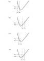
また、結合係数の変動範囲が存在する場合には、図9のように、周波数が可変範囲の上限値fmax又は下限値fminであるときに、結合係数が変動範囲の上限値kmax又は下限値kminとなるように、素子223及び素子227のインピーダンスを定める。すなわち、本実施形態の非接触給電システム200では、周波数が可変範囲の上限値fmax又は下限値fminであり、且つ結合係数が変動範囲の上限値kmax又は下限値kminであるときに、式(12)を満たすように素子223及び素子227の虚数インピーダンスが定められている。式(12)では、送電コイル213及び受電コイル221の自己インダクタンスとして、結合係数kの変動範囲内での変化に応じた自己インダクタンスの変化範囲のいずれかの値が用いられる。このように定めることにより、結合係数が変化した場合に、式(12)を満たす周波数fが存在する可能性を高めることができる。なお、図9(a)は、周波数が可変範囲の上限値fmaxであるときに、結合係数が変動範囲の下限値kminとなる場合を示している。図9(b)は、周波数が可変範囲の下限値fminであるときに、結合係数が変動範囲の下限値kminとなる場合を示している。図9(c)は、周波数が可変範囲の下限値fminであるときに、結合係数が変動範囲の上限値kmaxとなる場合を示している。図9(d)は、周波数が可変範囲の上限値fmaxであるときに、結合係数が変動範囲の上限値kmaxとなる場合を示している。Further, when there is a fluctuation range of the coupling coefficient, as shown in FIG. 9, when the frequency is the upper limit value fmax or the lower limit value fmin of the variable range, the coupling coefficient is the upper limit value kmax or the fluctuation range. The impedances of the
更に、周波数fの可変範囲で、式(12)を満たす周波数fと結合係数kとの関係が単調増加又は単調減少のグラフ(例えば、単調減少である図8のグラフ)で示される関係になっている場合、周波数の変更制御方法を第1実施形態で説明した方法よりもより容易に実施することができる。第1実施形態での方法は、式(23)より変化後の結合係数k2を求め、式(12)を満足する周波数f2を式(13)より算出する。一方、以下では、式(13)を用いずに周波数f2を求める方法を説明する。具体的には、式(20)より、α=1の成立時には、式(12)が成立するので、送電側制御部249は、αが1になるようにフィードバック制御を行う。例えば、送電側制御部249は、送電側検出部245及び受電側検出部253により検出された電流I1、I2の値に基づいてαを求め、αと1の差分に対してPID制御を行う。式(13)の多項式を解く必要がないため、送電側制御部249の計算負荷を抑えることが可能になる。Further, in the variable range of the frequency f, the relationship between the frequency f satisfying the equation (12) and the coupling coefficient k is a relationship indicated by a monotonically increasing or monotonically decreasing graph (for example, the graph of FIG. 8 that is monotonically decreasing). In this case, the frequency change control method can be performed more easily than the method described in the first embodiment. In the method according to the first embodiment, the coupling coefficient k2 after the change is obtained from Expression (23), and the frequency f2 that satisfies Expression (12) is calculated from Expression (13). On the other hand, hereinafter, a method of obtaining the frequency f2 without using the equation (13) will be described. Specifically, from equation (20), when α = 1 is established, equation (12) is established, and thus the power transmission
このように本実施形態では、周波数fと結合係数kと受電側直列素子223の虚数インピーダンスとが、式(12)を満たすことにより、電源211から受電側を見たときのインピーダンスZSは結合係数kに非依存となる。また、送電側並列素子217と受電側並列素子227とが式(31)を満たすことにより、インピーダンスZSは、第1実施形態と同様の式で表現され、素子217及び227のインピーダンスの値に影響されない。送電コイル213と受電コイル221との位置ずれやコイル間距離の変化により、結合係数kが変化した場合には、周波数fを式(12)が成立するように選択できる。すなわち、送電側制御部249は、結合係数kが変化した場合に、電源211から受電側を見たときのインピーダンスZSが結合係数kに非依存となるように、周波数fを調節するよう、構成されている。これにより、周波数fを変化させた場合に、結合係数kの変化に因ってインピーダンスZSが変わることはないため、インピーダンスZSの変動を抑えることができる。よって、インピーダンスZSが変動し難い分、交流電圧VSの変動を抑えることが可能になる。As described above, in this embodiment, when the frequency f, the coupling coefficient k, and the imaginary impedance of the power receiving
また、本実施形態では、受電側直列素子223をインダクタで構成することができる。このような構成の下、受電装置203が電力変換回路を含むような場合には、受電側直列素子223が高調波低減フィルタの役割を果たすため、負荷225に供給される交流電流の波形を理想的な正弦波に近づけることができる。 Moreover, in this embodiment, the power receiving
また、本実施形態では、受電側直列素子223をインダクタで構成するとともに、受電側並列素子227をキャパシタで構成することができる。これにより、受電側直列素子223及び受電側並列素子227の双方をキャパシタで構成する場合よりも、式(12)を満たす周波数fと結合係数kとの関係を示すグラフの傾きの大きさを大きくできる。よって、周波数fの有限の可変範囲でより広い結合係数kの変動範囲に対応可能となる。 In the present embodiment, the power receiving side
本発明を諸図面や実施形態に基づき説明してきたが、当業者であれば本願の請求の範囲内で本開示に基づき種々の変形や修正を行うことが可能である。従って、これらの変形や修正も本発明の範囲に含まれる。 Although the present invention has been described based on the drawings and embodiments, those skilled in the art can make various modifications and corrections based on the present disclosure within the scope of the claims of the present application. Accordingly, these variations and modifications are also included in the scope of the present invention.
上述の本発明の実施形態において、2つの態様の素子構成(図1及び図4)を説明したが、本発明はこの態様に限定されない。例えば、図10のように、送電コイル313に直列であって、送電側並列素子317よりも送電コイル側に接続される素子319が送電装置に設けられ、受電コイル321に直列であって、受電側並列素子327よりも受電コイル側に接続される素子329が受電装置に設けられてもよい。すなわち、素子319は、送電側並列素子317よりも送電コイル313に近い位置で送電コイル313に直列に接続されている。素子329は、受電側並列素子327よりも受電コイル321に近い位置で受電コイル321に直列に接続されている。素子319及び329は、虚数インピーダンスjZS1i−2及びjZS2i−2をそれぞれ有している。第1及び第2実施形態のように、回路方程式を解き、式(12)、式(31)及び式(40)が成立する場合には、式(33)が成立する。これにより、インピーダンスZSは、結合係数kに影響されないように(非依存となるように)構成される。図10のような回路構成の実施例としては、素子315及び323がそれぞれインダクタであり、素子317、319、327、329がそれぞれキャパシタである。また更なる変形例として、送電側直列素子315及び送電コイル313の間に、送電コイル313に対して並列又は直列に更なる素子(図示せず)が接続され、且つ受電側直列素子323及び受電コイル321の間に、受電コイル321に対して並列又は直列に更なる素子(図示せず)が接続されていたとしても、インピーダンスZSを結合係数kに非依存にすることは可能である。具体的には、送電装置301と受電装置303との素子構成を、送電コイル313及び受電コイル321を基準に対称(図10の、送電コイル313及び受電コイル321の中間に位置し両コイルの送電方向に直交する直線に関する線対称)とし、送電側の素子のインピーダンスを、受電側の対称の素子のインピーダンスの(L1/L2)倍にすればよい(式(40)参照)。In the above-described embodiment of the present invention, the element configuration of two aspects (FIGS. 1 and 4) has been described, but the present invention is not limited to this aspect. For example, as illustrated in FIG. 10, an
また、上述の本発明の実施形態の説明において、負荷のインピーダンスZ2rの変動については考慮していない。しかし、例えば、負荷がバッテリで構成されている場合、バッテリの充電率(SOC:State Of Charge)によって、負荷(バッテリ)のインピーダンスZ2rは変動する。この場合、式(16)や式(33)で表される電源から受電側を見たインピーダンスZSの実部は、負荷のインピーダンスZ2rの変動により変化する。但し、このような構成であっても、インピーダンスZSが、結合係数に非依存であることは、上述の実施形態と同様である。Further, in the above description of the embodiment of the present invention, the variation of the load impedance Z2r is not taken into consideration. However, for example, if the load is constituted by a battery, the charging rate of the battery: the (SOC State Of Charge), the impedance Z2r of the load (battery) varies. In this case, the real part of the impedance ZS when the power receiving side is viewed from the power source represented by the equation (16) or the equation (33) changes due to the fluctuation of the load impedance Z2r . However, even in such a configuration, the impedance ZS is independent of the coupling coefficient as in the above-described embodiment.
更に、式(39)に示される結合係数kと周波数fとの関係式にインピーダンスZ2rが含まれているため、負荷のインピーダンスZ2rが変動すると、図7や図8で表されるグラフの形状が変化する。しかし、インピーダンスZ2rに依らず、式(12)を満たす結合係数kと周波数fの組合せ(以下、特異解という)が存在する。以下、図4の回路構成における特異解について説明する。説明の便宜上、図4に示される回路構成の素子215、217、223、227はそれぞれキャパシタであり、素子215、217、223、227のキャパシタンスはそれぞれ、CS1、CP1、CS2、CP2で示される。なお、これらの素子の一部がインダクタで構成されてもよい。また、特異解の存在は、図4の回路構成に限定されるものではなく、図10の回路構成でも同様に特異解を求めることができる。Further, since the impedance Z2r is included in the relational expression between the coupling coefficient k and the frequency f shown in the equation (39), if the load impedance Z2r changes, the graphs shown in FIG. 7 and FIG. The shape changes. However, there is a combination of the coupling coefficient k and the frequency f satisfying the equation (12) (hereinafter referred to as a singular solution) regardless of the impedance Z2r . Hereinafter, the singular solution in the circuit configuration of FIG. 4 will be described. For convenience of explanation, the
式(29)から電流I1とI2の関係式を求め、式(12)が成立すると、式(41)が成立する。なお、ZS1i=−1/(ωCS1)、ZP1i=−1/(ωCP1)、ZS2i=−1/(ωCS2)、ZP2i=−1/(ωCP2)である。When a relational expression between the currents I1 and I2 is obtained from the expression (29) and the expression (12) is satisfied, the expression (41) is satisfied. Note that ZS1i = −1 / (ωCS1 ), ZP1i = −1 / (ωCP1 ), ZS2i = −1 / (ωCS2 ), ZP2i = −1 / (ωCP2 ).
式(41)を変形すると、式(42)が得られる。 By transforming equation (41), equation (42) is obtained.
式(43)が成立する場合、Z2rの値に依らず、式(42)は成立する。If the expression (43) issatisfied, regardless of the value ofZ 2r, equation (42) is satisfied.
式(43)を解くと、キャパシタンスCS2、CP2の解として、正の解と負の解が得られるが、実際のキャパシタンスCS2、CP2が正の値を持つため、正の解を採用する。なお、負の解は、素子223がキャパシタではなくインダクタであることを意味する。Solving equation (43), as a solution of the capacitanceCS2, C P2, although positive solution and negative solutions are obtained, because the actual capacitanceCS2, C P2 has a positive value, the positive solution adopt. Note that a negative solution means that the
受電コイル121のインダクタンスが既知である場合、所定の周波数及び結合係数を式(43)に代入することにより、この所定の周波数及び結合係数が特異解となる素子のインピーダンスが求められる。例えば、式(43)に代入する所定の周波数の値を、可変範囲の上限値fmax又は下限値fminとし、所定の結合係数の値を、変動範囲の下限値kminとする。こうすることにより、可変範囲の境界に特異解を配置することができる。When the inductance of the
続いて、負荷225のインピーダンスZ2rが変動した場合の結合係数kと周波数fのグラフの形状の変化について、図11を用いて説明する。まず、図11(a)のように、特異解S1が、周波数fの可変範囲内(境界は除く)にあり、結合係数kの変動範囲内(境界は除く)にある場合を説明する。負荷225のインピーダンスZ2rが大きくなると、結合係数kと周波数fのグラフは、グラフG3からグラフG4のように変化する。なお、周波数の初期値としてfmaxが設定されているときに、結合係数がk5(>kmin)で示される場合を説明する。この場合、グラフG3では、周波数を減少させることにより、式(12)を満たす周波数f5が見つかる。しかし、グラフG4では、周波数を増加させる必要があるが、fmaxよりも周波数を大きくすることはできないため、式(12)を満たす周波数を選択することはできない。そのため、グラフG4においてfmaxで式(12)を満たす結合係数がk6である場合、結合係数k(kmin≦k<k6)では、式(12)を満たす周波数を選択できない。実際の結合係数k(kmin≦k<k6)が、周波数fmaxで式(12)を満たす結合係数k6よりも小さい場合には、電源111から受電側を見たインピーダンスZSが容量性負荷になる。電源111がインバータ回路で構成されている場合には、ソフトスイッチングを実現できない。Next, a change in the shape of the graph of the coupling coefficient k and the frequency f when the impedanceZ2r of the load 225 varies will be described with reference to FIG. First, as shown in FIG. 11A, the case where the singular solution S1 is within the variable range of the frequency f (excluding the boundary) and within the variation range of the coupling coefficient k (excluding the boundary) will be described. When the impedanceZ2r of the load 225 increases, the graph of the coupling coefficient k and the frequency f changes from the graph G3 to the graph G4. A case where the coupling coefficient is represented by k5 (> kmin ) when fmax is set as the initial value of the frequency will be described. In this case, the graph G3, by reducing the frequency, we find a frequencyf 5 which satisfies the expression (12). However, in the graph G4, it is necessary to increase the frequency. However, since the frequency cannot be made larger than fmax , it is not possible to select a frequency that satisfies Equation (12). Therefore, when the coupling coefficient satisfies the formula (12) withf max in the graph G4 isk 6, the coupling coefficientk (k min ≦ k <k 6), can not be selected frequencies satisfying Eq (12). When the actual coupling coefficient k (kmin ≦ k <k6 ) is smaller than the coupling coefficient k6 satisfying the expression (12) at the frequency fmax , the impedance ZS viewed from the
一方、図11(b)のように、特異解S2が、周波数fの可変範囲の上限値fmaxであり、結合係数kの変動範囲の下限値kminである場合を説明する。負荷225のインピーダンスZ2rが大きくなると、結合係数kと周波数fのグラフは、グラフG3からグラフG5のように変化する。この場合、周波数がfmaxであり、結合係数がk5であるとき、グラフG3では、周波数を減少させることにより、式(12)を満たす周波数f5−1が見つかる。また、グラフG5でも、周波数を減少させることにより、式(12)を満たす周波数f5−2が見つかる。図11(a)とは異なり、結合係数kがkmin≦k<k6の範囲内であっても、式(12)を満たす周波数を選択できる。そのため、周波数fの可変範囲で式(12)を満たす結合係数の範囲を広げることができる。また、実際の結合係数kが、周波数fmaxで式(12)を満たす結合係数kmin以上になるので、電源111から受電側を見たインピーダンスZSが誘導性負荷になる。電源111がインバータ回路で構成されている場合には、ソフトスイッチングを実現できる。更に、インピーダンスZ2rの変動により、グラフが変化しても、周波数の減少という同様の制御により、式(12)を満たす周波数を選択することができる。On the other hand, as shown in FIG. 11B, the case where the singular solution S2 is the upper limit value fmax of the variable range of the frequency f and the lower limit valuekmin of the fluctuation range of the coupling coefficient k will be described. When the impedanceZ2r of the load 225 increases, the graph of the coupling coefficient k and the frequency f changes from the graph G3 to the graph G5. In this case, when the frequency is fmax and the coupling coefficient is k5 , in the graph G3, the frequency f5-1 that satisfies the equation (12) is found by decreasing the frequency. Also in the graph G5, by reducing the frequency, the frequency f5-2 that satisfies the equation (12) is found. Unlike FIG. 11A, even if the coupling coefficient k is within the range of kmin ≦ k <k6, a frequency satisfying the expression (12) can be selected. Therefore, it is possible to widen the range of the coupling coefficient that satisfies Expression (12) in the variable range of the frequency f. Further, since the actual coupling coefficient k is equal to or higher than the coupling coefficientkmin satisfying the expression (12) at the frequency fmax , the impedance ZS viewed from the
また、上述の本発明の実施形態において、送電装置の電源の送電効率について説明したが、非接触給電システム全体の電力効率を向上させるためには、受電装置内の効率も高める必要がある。以下、図4を用いて受電装置内の効率向上について検討する。説明の便宜上、図4に示される回路構成の素子223、227はそれぞれキャパシタであり、素子223、227のキャパシタンスはそれぞれ、CS2、CP2で示される。In the above-described embodiment of the present invention, the power transmission efficiency of the power source of the power transmission device has been described. However, in order to improve the power efficiency of the entire non-contact power feeding system, it is also necessary to increase the efficiency in the power receiving device. Hereinafter, efficiency improvement in the power receiving apparatus will be examined with reference to FIG. For convenience of explanation, the
受電コイル221には、送電コイル213との磁気結合により起電力Vmが誘導され、受電装置203は、図12のような等価回路で示される。起電力Vmは、式(44)で示される。An electromotive forceVm is induced in the
また、図12の回路方程式は、式(45)になる。Moreover, the circuit equation of FIG. 12 becomes Formula (45).
式(45)に、式(44)を代入し、電流I2について解くと、式(46)が導かれる。Substituting equation (44) into equation (45) and solving for current I2 yields equation (46).
受電装置内の効率を高めるためには、受電コイル221に誘導される起電力と受電コイル221の電流I2との位相差を0°に近づければよい。よって、位相差が0°であり、式(46)の虚数部が存在しないときに、受電装置内の効率が最も高くなる。これは、式(47)が成立するときに相当する。この場合、負荷225に所望電力を供給する場合、受電装置内の無効電力が存在しないので、受電コイルの電流を小さくすることができ、素子又は配線での発熱を抑えることができる。In order to increase the efficiency in the power receiving apparatus, the phase difference between the electromotive force induced in the
受電装置内の効率を高めるための条件式は、図4の回路構成に限定して導かれるものではなく、図10の回路構成でも同様にして導かれる。 The conditional expression for increasing the efficiency in the power receiving device is not limited to the circuit configuration of FIG. 4, and is similarly derived in the circuit configuration of FIG. 10.
なお、図4の回路構成では、受電コイル221のインピーダンスが予め定められ、周波数f(角周波数ω)、結合係数k及び負荷のインピーダンスZ2rのそれぞれに対して任意の値が選択される場合、変数は、素子223及び227のインピーダンスの2つである。そのため、式(12)の成立条件である式(41)と、最大効率条件である式(47)との2つの条件式が与えられた場合、素子223及び227のインピーダンスはそれぞれ特定の値に定まる。つまり、式(12)の成立条件と最大効率条件を考慮すると、所望の周波数fと結合係数kが式(43)を満足しなくなる。また、特異解を所望の値に設定する場合、式(43)で素子223及び227のインピーダンスはそれぞれ特定の値に定まるため、最大効率条件は同時に満足されなくなる。In the circuit configuration of FIG. 4, when the impedance of the
一方、図10の回路構成では、素子323及び327に加え、素子329が設けられているため、変数は3つとなる。説明の便宜上、図10の回路構成の素子323、327、329はそれぞれキャパシタであり、素子323、327、329のキャパシタンスはそれぞれ、CS2、CP2、CSf2で示される。式(12)が成立すると、式(41)と同様に、式(48)が成立し、式(48)から特異解を与える式(49)が得られる。また、上記の図4の回路構成の場合と同様に、最大効率条件として式(50)が得られる。On the other hand, in the circuit configuration of FIG. 10, since the
変数が、素子323、327、329のインピーダンスの3つであり、条件式が式(49)の2式と式(50)の1式との合計3式であるため、特異解を所望の値に設定しつつ、最大効率条件を満足する素子323、327、329のインピーダンスがそれぞれ特定の値に定まる。また、任意の特性を定める最大効率条件以外の別条件がある場合にも、この別条件と式(49)を組み合わせることにより、特異解を所望の値に設定しつつ、別条件を満足させる素子のインピーダンスが定まる。例えば、素子329のインピーダンスがある値に定まると、式(49)を満足する素子323及び327のインピーダンスはそれぞれ特定の値に定まる。そのため、所望の条件を式として定義することが困難な場合には、素子329のインピーダンスがある値である場合に、所望の条件が満たされるかを確認することができる。所望の条件が満たされていない場合には、素子329のインピーダンスを変更し、所望の条件が満たされるように、素子329のインピーダンスを調整することができる。 Since the variables are the three impedances of the
また、上述の本発明の実施形態の説明において、素子のインピーダンスは固定であり、変化しないものとしたが、本発明はこの態様に限定されない。例えば、受電装置の素子を可変素子(可変インダクタや可変キャパシタ)で構成することができる。この場合、結合係数kの変化時に、周波数fではなく受電装置の素子のインピーダンス(虚数インピーダンス)を、又は周波数fだけでなく受電装置の素子のインピーダンス(虚数インピーダンス)を変更することにより、電源から受電側を見たときのインピーダンスを結合係数に非依存とすることができる。なお、上記素子の虚数インピーダンスにおける変更の制御を、上述した送電側制御部が行ってもよい。この場合、送電側制御部は、以下を行うように構成されている。具体的には、送電側制御部は、結合係数kが変化した場合に、電源から受電側を見たときのインピーダンスが結合係数kに非依存となるように、素子の虚数インピーダンスの値を特定できる。そして、送電側制御部は、素子の虚数インピーダンスをこの値に設定するよう、通信部を介して受電側制御部に指示できる。 In the above description of the embodiment of the present invention, the impedance of the element is fixed and does not change, but the present invention is not limited to this aspect. For example, the element of the power receiving device can be configured by a variable element (a variable inductor or a variable capacitor). In this case, when the coupling coefficient k changes, the impedance of the power receiving device (imaginary impedance) is changed instead of the frequency f, or the impedance of the power receiving device (imaginary impedance) is changed in addition to the frequency f. The impedance when looking at the power receiving side can be made independent of the coupling coefficient. Note that the above-described power transmission side control unit may control the change in the imaginary impedance of the element. In this case, the power transmission side control unit is configured to perform the following. Specifically, when the coupling coefficient k changes, the power transmission side control unit specifies the value of the imaginary impedance of the element so that the impedance when the power reception side is viewed from the power source is independent of the coupling coefficient k. it can. The power transmission side control unit can instruct the power reception side control unit via the communication unit to set the imaginary impedance of the element to this value.
また、上述の本発明の実施形態や変形例の説明において、周波数や素子の虚数インピーダンスは、送信側制御部によって制御され変更されている。しかし、上述した受電側制御部が、周波数や素子の虚数インピーダンスを制御して変更するように構成されてもよい。この場合、受電側制御部は、制御に必要な情報を上述した通信部を介して送信側制御部から取得してもよい。すなわち、受電側制御部は、結合係数kが変化した場合に、電源から受電側を見たときのインピーダンスが結合係数kに非依存となるように、上記電源が出力する交流電力の周波数の値を特定できる。そして、受電側制御部は、電源が出力する交流電力の周波数をこの値に設定するように送電側制御部に指示できる。また、受電側制御部は、結合係数kが変化した場合に、電源から受電側を見たときのインピーダンスが結合係数kに非依存となるように、受電装置の素子の虚数インピーダンスを調節してもよい。 In the above description of the embodiments and modifications of the present invention, the frequency and the imaginary impedance of the element are controlled and changed by the transmission side control unit. However, the power receiving side control unit described above may be configured to control and change the frequency and the imaginary impedance of the element. In this case, the power receiving side control unit may acquire information necessary for control from the transmission side control unit via the communication unit described above. That is, when the coupling coefficient k changes, the power receiving side control unit determines the frequency value of the AC power output from the power source so that the impedance when the power receiving side is viewed from the power source is independent of the coupling coefficient k. Can be identified. And the power receiving side control part can instruct | indicate to the power transmission side control part to set the frequency of the alternating current power which a power supply outputs to this value. In addition, the power receiving side control unit adjusts the imaginary impedance of the elements of the power receiving device so that the impedance when the power receiving side is viewed from the power source is independent of the coupling coefficient k when the coupling coefficient k changes. Also good.
さらに、本発明の非接触給電システムは、上記実施形態や変形例の作用効果が得られるように構成されていればよいため、本発明の非接触給電システムが、結合係数kが変化した場合に、電源から受電側を見たときのインピーダンスが結合係数kに非依存となるように、上記電源が出力する交流電力の周波数及び素子の虚数インピーダンスの少なくとも一方を調節するよう、構成されていればよい。 Furthermore, since the non-contact power feeding system of the present invention only needs to be configured so as to obtain the effects of the above-described embodiments and modifications, the non-contact power feeding system of the present invention can be used when the coupling coefficient k changes. If it is configured to adjust at least one of the frequency of the AC power output from the power source and the imaginary impedance of the element so that the impedance when the power receiving side is viewed from the power source is independent of the coupling coefficient k Good.
可変キャパシタや可変インダクタの実施例は、図13(a)〜(d)のように、インピーダンスの異なる複数のキャパシタ431a〜431d又はインダクタ433a〜433dがスイッチング素子SW1〜SW6を介して接続された回路である。受電側制御部がスイッチング素子SW1〜SW6をスイッチングすることでキャパシタ431a〜431d及びインダクタ433a〜433dのうち使用される素子を切り替えることができ、回路のキャパシタンス及びインダクタンスの値を変化させることができる。回路のキャパシタンス又はインダクタンスの値が変化することにより、式(12)を満たす周波数fと結合係数kとの関係が変わる。そのため、回路のキャパシタンス又はインダクタンスの値を変えることにより、周波数fの可変範囲において式(12)を満たす結合係数kの範囲を広げることができる。また、可変キャパシタや可変インダクタは、図13(a)〜(d)のようにキャパシタンスやインダクタンスの値が選択的に不連続に変化する回路だけでなく、スライダックやトリマコンデンサ等のように上記値が連続的に変化する回路を含む。 Examples of variable capacitors and variable inductors are circuits in which a plurality of
また、上述の本発明の実施形態の説明では、非接触給電システム内における電圧や電流が、正弦波であることを前提としている。しかし、これらの電圧や電流が、正弦波ではなく、複数の周波数成分を含む場合には、本発明は、基本波成分に対して適用できる。 In the above description of the embodiment of the present invention, it is assumed that the voltage and current in the non-contact power feeding system are sine waves. However, when these voltages and currents include a plurality of frequency components instead of a sine wave, the present invention can be applied to the fundamental wave component.
また、送電コイル、受電コイル及び各素子に抵抗成分が存在する場合は、抵抗成分を無視して理想的なインダクタンス(コイル)やキャパシタンスとみなすことにより、本発明を利用できる。更に、非接触給電システム内の配線における抵抗成分及びリアクタンス成分が存在する場合も、これらの抵抗成分及びリアクタンス成分を無視することにより、本発明を利用できる。 Moreover, when a resistance component exists in the power transmission coil, the power reception coil, and each element, the present invention can be used by ignoring the resistance component and considering it as an ideal inductance (coil) or capacitance. Furthermore, even when there are resistance components and reactance components in the wiring in the non-contact power supply system, the present invention can be used by ignoring these resistance components and reactance components.
また、上記実施形態では、非接触給電システムの適用例としては、移動体、家電製品又は医療機器の、充電システムや駆動システムであるとしたが、本発明はこの態様に限定されない。例えば、本発明は、コイルの電磁誘導の原理を利用する種々の回路装置に適用することができる。具体的には、本発明の非接触給電システムを絶縁型のDCDCコンバータに組み込むことができる。 Moreover, in the said embodiment, although it was set as the charging system and drive system of a mobile body, household appliances, or a medical device as an application example of a non-contact electric power feeding system, this invention is not limited to this aspect. For example, the present invention can be applied to various circuit devices that use the principle of electromagnetic induction of coils. Specifically, the non-contact power feeding system of the present invention can be incorporated into an insulated DCDC converter.
また、上記実施形態では、結合係数が変化した場合に、式(12)が成立するように非接触給電システムの各パラメータ(素子のインピーダンス、周波数)が定められるが、本発明はこの態様に限定されない。具体的には、結合係数が変化した場合に、式(51)が成立するように非接触給電システムの各パラメータ(素子のインピーダンス、周波数)が定められてもよい。 Further, in the above embodiment, when the coupling coefficient changes, each parameter (element impedance, frequency) of the non-contact power feeding system is determined so that Expression (12) is satisfied, but the present invention is limited to this aspect. Not. Specifically, when the coupling coefficient changes, each parameter (element impedance, frequency) of the non-contact power feeding system may be determined so that Expression (51) is satisfied.
まず、図1の回路構成を参照して説明する。式(51)が成立する場合、式(11)及び式(51)より、式(52)が成立する。なお、KIは、予め定められた係数(定数)である。First, a description will be given with reference to the circuit configuration of FIG. When Expression (51) is established, Expression (52) is established from Expression (11) and Expression (51). Incidentally,K I is a predetermined coefficient (constant).
ここで、式(51)が成立するように非接触給電システム100の各パラメータ(素子のインピーダンス、周波数、結合係数)が決定又は制御される。この場合、式(52)を式(14)に代入することにより、式(14)は、式(53)になる。 Here, each parameter (element impedance, frequency, coupling coefficient) of the non-contact
よって、電源111から受電側を見たインピーダンスZSは、式(54)で示される。Therefore, the impedance ZS when the power receiving side is viewed from the
式(54)より、電源111から受電側を見たインピーダンスZSは、結合係数kを含まない。よって、インピーダンスZSは結合係数kに非依存となる。つまり、結合係数が変化しても式(51)が成立するように周波数fが選択されれば(定められれば)、インピーダンスZSは結合係数kに非依存となる。つまり、係数KIが定数で変化しないため、式(51)の右辺は一定の値である。よって、結合係数が変化しても、電流I1とI2の比が一定であり続けるように、周波数f及び虚数インピーダンスZS2iが定められる。その結果、インピーダンスZS、ひいては交流電圧VS(=ZS/I1)は、変動し難くなる。なお、他の実施形態と同様、受電装置103の素子123が可変素子である場合には、周波数fではなく、式(51)が成立するように素子123のインピーダンスZS2iを変更してもよい。つまり、周波数f、虚数インピーダンスZS2i及び結合係数kが、式(51)を満たすことに基づく値であれば、インピーダンスZSは結合係数kに非依存となる。From the equation (54), the impedance ZS when the power receiving side is viewed from the
また、式(54)において、虚数インピーダンスZS1iが式(55)を満たすときには、式(54)の虚部が打ち消され、式(56)のようにインピーダンスZSは実部のみを有する。このとき、電源111の力率は100%となる。一方、虚数インピーダンスZS1iの値を式(55)の値からずらすことにより、インピーダンスZSが結合係数kに依存することなく、力率を所望の値にすることができる。Further, in the equation (54), when the imaginary impedance ZS1i satisfies the equation (55), the imaginary part of the equation (54) is canceled out, and the impedance ZS has only the real part as in the equation (56). At this time, the power factor of the
なお、式(51)を満たす値から周波数fをずらすと、式(57)が成立する。εは、誤差である。 If the frequency f is shifted from a value satisfying the equation (51), the equation (57) is established. ε is an error.
このとき、送電コイル113から受電側を見たインピーダンスZ1は、式(58)で表現され、電源111から受電側を見たインピーダンスZSは、式(59)で表現される。式(59)より、誤差εが発生しても、インピーダンスZSは結合係数kに非依存である。At this time, the impedance Z1 when the power reception side is viewed from the
虚数インピーダンスZS1iが式(55)を満たすときには、式(59)は、式(60)となる。式(60)を式(56)と比較すると、式(51)を満たす値から周波数fをずらすことは、インピーダンスZSの実部と力率を制御できることも意味している。また、パラメータ(例えば、インダクタンスL1及びL2)の変動や負荷125の変動が生じた場合にも、式(57)を満たすように周波数fを選ぶことにより、同一電力を負荷125に供給することもできる。When the imaginary impedance ZS1i satisfies Expression (55), Expression (59) becomes Expression (60). Comparing equation (60) with equation (56), shifting frequency f from a value satisfying equation (51) also means that the real part and power factor of impedance ZS can be controlled. Further, even when a change in parameters (for example, inductances L1 and L2) or a change in the
続いて、図14の回路構成を参照して説明する。図14の回路構成は、図4の回路構成に素子519が追加された回路構成である。つまり、図14の送電装置501の構成要素511、513、515、517及び受電装置503の構成要素521、523、527は、図4の送電装置201の構成要素211、213、215、217及び受電装置203の構成要素221、223、227とそれぞれ同一である。また、受電装置503に接続されている負荷525は、受電装置203に接続されている負荷225と同一である。これらの構成要素の説明は、図4の説明と重複するため省略する。 Next, description will be made with reference to the circuit configuration of FIG. The circuit configuration of FIG. 14 is a circuit configuration in which an
素子519は、送電コイル513に直列に接続され、且つ素子517よりも送電コイル側に接続され、虚数インピーダンスjZS1i-2を有する。すなわち、素子519は、素子517よりも送電コイル513に近い位置で送電コイル513に直列に接続されている。素子519は、図10の素子319に対応する。素子519は、例えば、インダクタ(リアクトル、コイル)やキャパシタ等のリアクタンス素子、又はそれらの組合せの複数の素子により構成される。The
図14の回路方程式を立てると、式(61)になる。 When the circuit equation of FIG. 14 is established, Equation (61) is obtained.
式(52)が成立する場合、素子519から受電側を見たインピーダンスZ1C(素子519を含むインピーダンス)を求めると、式(62)で示される値になり、この式は結合係数kを含まない。When the equation (52) is established, the impedance Z1C (impedance including the device 519) viewed from the power receiving side from the
ここで、式(63)が成立するように素子519のインピーダンスの値が決定されていると、インピーダンスZ1Cは、式(64)のようになる。なお、素子519のインピーダンスが0にならないように、係数KIは0よりも大きく1よりも小さい値、又は1よりも大きい値であるとする。Here, when the impedance value of the
すると、素子517から受電側を見たインピーダンスZ1(素子517を含むインピーダンス)を求めると式(65)で示される値になり、この式は結合係数kを含まない。Then, when the impedance Z1 (impedance including the element 517) as seen from the
式(66)が成立するように素子517及び素子527のインピーダンスの値が決定されていると、式(65)及び式(66)より、式(67)が成立する。 When the impedance values of the
よって、電源511から受電側を見たインピーダンスZS(電源511を含まないインピーダンス)は、式(68)で示される。Therefore, the impedance ZS (impedance not including the power supply 511) when the power reception side is viewed from the
式(68)より、電源511から受電側を見たインピーダンスZSは、結合係数kに非依存となる。また、インピーダンスZSの実部は、負荷525のインピーダンスと送電コイル513及び受電コイル521の自己インダクタンスと係数KIとのみで表現され、素子515、517、519、523、527のインピーダンスの影響を受けない。From equation (68), the impedance ZS when the power receiving side is viewed from the
更に、式(68)において、虚数インピーダンスZS1iが式(69)を満たすときには、式(68)の虚部が打ち消され、式(70)のようにインピーダンスZSは実部のみを有する。このとき、電源511の力率は100%となる。一方、虚数インピーダンスZS1iの値を式(69)の値からずらすことにより、インピーダンスZSが結合係数kに依存することなく、力率を所望の値にすることができる。Further, in the equation (68), when the imaginary impedance ZS1i satisfies the equation (69), the imaginary part of the equation (68) is canceled, and the impedance ZS has only a real part as in the equation (70). At this time, the power factor of the
なお、図10の回路構成では、式(71)が成立するように、素子319と素子329とのインピーダンスの値が決定されれば、上記と同様の式導出が可能である。 In the circuit configuration of FIG. 10, if the impedance values of the
ここで、式(52)は、以下の式(72)に変形される。 Here, the equation (52) is transformed into the following equation (72).
式(72)では、式(13)と比べ、実際の結合係数kが見掛け上の結合係数kaに変わっただけである。よって、式(12)に基づいて上述された非接触給電システムの設計方法・制御方法は全て、式(52)に基づく非接触給電システムの設計方法・制御方法に適用することができる。In equation (72), compared to Equation (13) is only changed to the actual coupling coefficient ka on the coupling coefficient k is apparent. Therefore, all of the design method and control method of the non-contact power supply system described above based on the equation (12) can be applied to the design method and control method of the non-contact power supply system based on the equation (52).
続いて、係数KIが1以外であると、係数KIが1である場合に比べ、受電コイルに流れる電流I2がどのように変化するかについて、図1及び図4の回路構成を参照して、説明する。Subsequently, the coefficient KI is non 1, whether the coefficient KI is compared with the
係数KIが1である場合、図1の回路構成では、式(11)及び式(12)より、式(73)が成立する。If coefficientK I is 1, in the circuit configuration of FIG. 1, the equation (11) and (12), equation (73) holds.
式(73)の左辺は、受電装置103と負荷125とから構成される回路の応答倍率Q(ω)に相当する。応答倍率Q(ω)は、この回路の共振周波数ωC(=−ZS2i/L2)で、共振倍率QC(ωCL2/Z2r)となる。式(73)を満足する周波数(ω0)におけるQ(ω0)が大きくなると、QCも比例して大きくなる。よって、式(12)(又は式(73))が成立することは、式(74)の関係が成立することに言い換えられる。The left side of Expression (73) corresponds to the response magnification Q (ω) of the circuit configured by the
つまり、式(12)が成立するときには、結合係数kが小さくなった場合、共振倍率QCが大きくなる。That is, when the equation (12) is satisfied, if the coupling coefficient k is decreased, the resonance magnification QC increases.
ここで、図4の回路構成における応答倍率について説明する。図4の応答倍率Q(ω)は、式(75)になる。 Here, the response magnification in the circuit configuration of FIG. 4 will be described. The response magnification Q (ω) in FIG. 4 is expressed by Equation (75).
共振倍率QCは、式(75)の分母の虚部が0になる場合であるため、式(76)になる。Resonance magnificationQ C are the case where the imaginary part of the denominator of the equation (75) becomes 0, the equation (76).
ここで、負荷225に流れる電流ILと受電コイル221に流れる電流I2との比は式(77)になる。Here, the ratio of the currentI 2 flowing through the
式(76)は、式(77)より、式(78)になる。 Expression (76) becomes Expression (78) from Expression (77).
式(74)および式(78)より、式(79)の関係が成立することになる。 From the equations (74) and (78), the relationship of the equation (79) is established.
式(79)は、結合係数kが小さくなるほど、受電コイル221に流れる電流I2が大きくなることを表している。Expression (79) indicates that the current I2 flowing through the
ここまで、係数KIが1である場合(つまり、式(12)が成立する場合)について説明してきたが、係数KIが1以外である場合の受電コイルに流れる電流I2の変化について説明する。式(51)が成立する場合、式(73)ではなく、式(80)が成立する。Up to this point, if the coefficient KI is 1 (i.e., if the expression (12) is satisfied) have been described, the coefficient KI is the change in current I2 flowing in the receiving coil when it is other than 1 Description To do. When Expression (51) is satisfied, Expression (80) is satisfied instead of Expression (73).
式(79)の導出と同様、式(51)が成立することは、式(81)の関係が成立することになる。 As in the derivation of Equation (79), the establishment of Equation (51) establishes the relationship of Equation (81).
負荷225に同一の電力を供給する場合、係数KIを0<KI<1の範囲にとることで、式(12)が成立する場合と比較して、受電コイル221に流れる電流I2を小さくすることができる。When the same electric power is supplied to the
例えば、非接触給電システムを電気自動車の充電システムに適用する場合、受電装置は、電気自動車に搭載されることになる。この場合、電気自動車への設置場所の制限の点で、受電装置の小型化が求められることがある。受電装置を小型化するためには、例えば、受電コイルを形成する導線を細くすることがある。導線を細くすると、導線の電気抵抗が増え、発熱量が増える。そこで、上記(73)が示すように、係数KIを0<KI<1に設定することにより、式(12)が成立する場合と比較して電流I2を小さくすることができ、発熱量を低減することが可能になる。For example, when the non-contact power supply system is applied to a charging system for an electric vehicle, the power receiving device is mounted on the electric vehicle. In this case, the power receiving device may be required to be downsized in terms of the restriction of the installation location in the electric vehicle. In order to reduce the size of the power receiving device, for example, the conducting wire forming the power receiving coil may be thinned. If the conducting wire is made thin, the electrical resistance of the conducting wire increases and the amount of heat generation increases. Therefore, as shown in (73) above, by setting the coefficient KI to 0 <KI <1, the current I2 can be reduced as compared with the case where the equation (12) is satisfied, and the heat generation The amount can be reduced.
なお、上記と同様にして、送電コイル213に流れる電流I1が大きくなることを抑えたい場合には、1<KIを満たすように係数KIを設定すればよい。Incidentally, in the same manner as described above, if it is desired to suppress that the current I1 flowing through the
上記実施形態及び変形例では、送電装置と受電装置とを備える非接触給電システムが説明されている。しかし、本発明はこの構成に限定されず、電源からある周波数の交流電力が入力される送電コイルを含む送電装置から非接触で電力を受ける受電装置に本発明が適用されてもよい。この受電装置は、上記実施形態及び変形例で説明された受電装置103、203又は303と同様の構成を備えている。すなわち、本発明の受電装置は、ある結合係数で上記送電コイルと磁気結合する受電コイルと、この受電コイルに直列に接続され、虚数インピーダンスjZS2iを有する受電側直列素子(第1の受電側直列素子)と、を含む。上記受電コイルは、受電コイル121、221又は321と同様の構成を備え、上記受電側直列素子は、素子123、223又は323と同様の構成を備えていてもよい。また、本発明の受電装置では、上記電源が出力する交流電力の周波数及び上記受電側直列素子の虚数インピーダンスが、結合係数kが変化した場合に、上記電源から受電側を見たときのインピーダンスが結合係数kに非依存となるように定められていればよい。言い換えれば、本発明の受電装置は、結合係数kが変化した場合に、上記電源から受電側を見たときのインピーダンスが結合係数kに非依存となるように、上記電源が出力する交流電力の周波数及び上記受電側直列素子の虚数インピーダンスの少なくとも一方を調節するよう、構成されていればよい。上記受電装置は、通信部等を介して上記電源に周波数の変更を指示してもよい。In the said embodiment and modification, the non-contact electric power feeding system provided with a power transmission apparatus and a power receiving apparatus is demonstrated. However, the present invention is not limited to this configuration, and the present invention may be applied to a power receiving device that receives power in a non-contact manner from a power transmitting device including a power transmitting coil to which AC power having a certain frequency is input from a power source. This power receiving apparatus has the same configuration as that of the
100、200、300、500 非接触給電システム
101、201、301、501 送電装置
103、203、303、503 受電装置
111、211、311、511 電源
113、213、313、513 送電コイル
115、215、315、515 素子(送電側直列素子、第2の送電側直列素子)
217、317、517 素子(送電側並列素子)
121、221、321、521 受電コイル
123、223、323、523 素子(第1の受電側直列素子)
125、225、325、525 負荷
227、327、527 素子(受電側並列素子)
141、241 交流電力出力部
143、243 送電部
145、245 送電側検出部
147、247 送電側通信部
148、248 記憶部
149、249 送電側制御部
151、251 受電部
153、253 受電側検出部
155、255 受電側通信部
157、257 受電側制御部
319、519 素子(第1の送電側直列素子)
329 素子(第2の受電側直列素子)
431a、431b、431c、431d キャパシタ
433a、433b、433c、433d インダクタ
SW1、SW2、SW3、SW4、SW5、SW6 スイッチング素子100, 200, 300, 500 Non-contact
217, 317, 517 element (transmission-side parallel element)
121, 221, 321, 521
125, 225, 325, 525
141, 241 AC
329 elements (second power receiving side series element)
431a, 431b, 431c,
Claims (23)
Translated fromJapanese前記送電装置は、電源からある周波数の交流電力が入力される送電コイルを含み、
前記受電装置は、ある結合係数で前記送電コイルと磁気結合する受電コイルと、前記受電コイルに直列に接続され、虚数インピーダンスjZS2iを有する第1の受電側直列素子とを含み、
前記周波数と前記結合係数と前記虚数インピーダンスとは、
を満たすことに基づく値である、
非接触給電システム。A non-contact power feeding system including a power transmitting device and a power receiving device,
The power transmission device includes a power transmission coil to which AC power of a certain frequency is input from a power source,
The power receiving device includes a power receiving coil that is magnetically coupled to the power transmitting coil with a certain coupling coefficient, and a first power receiving side series element connected in series to the power receiving coil and having an imaginary impedance jZS2i ,
The frequency, the coupling coefficient, and the imaginary impedance are:
Is based on satisfying the
Contactless power supply system.
前記送電コイルに並列に接続され、虚数インピーダンスjZP1iを有する送電側並列素子と、
前記送電側並列素子よりも前記送電コイルに近い位置で前記送電コイルに直列に接続され、虚数インピーダンスjZS1i-2を有する第1の送電側直列素子と
を更に含み、
前記受電装置は、前記受電側直列素子よりも前記受電コイルに近い位置で前記受電コイルに並列に接続され、虚数インピーダンスjZP2iを有する受電側並列素子を更に含み、
前記第1の送電側直列素子の前記虚数インピーダンスは、
前記送電側並列素子及び前記受電側並列素子の前記虚数インピーダンスは、
請求項2に記載の非接触給電システム。The power transmission device is:
A power transmission side parallel element connected in parallel to the power transmission coil and having an imaginary impedance jZP1i ;
A first power transmission side series element connected in series to the power transmission coil at a position closer to the power transmission coil than the power transmission side parallel element and having an imaginary impedance jZS1i-2 ;
The power receiving device further includes a power receiving side parallel element connected in parallel to the power receiving coil at a position closer to the power receiving coil than the power receiving side series element, and having an imaginary impedance jZP2i ,
The imaginary impedance of the first power transmission side series element is:
The imaginary impedance of the power transmission side parallel element and the power reception side parallel element is:
The non-contact electric power feeding system according to claim 2.
前記結合係数の変動範囲が定められ、
前記第1の受電側直列素子及び前記受電側並列素子の前記虚数インピーダンスは、前記周波数が前記可変範囲の上限値又は下限値であり、且つ前記結合係数が前記変動範囲の上限値又は下限値であるときに、前記式(1)を満たすように定められている、
請求項3に記載の非接触給電システム。A variable range of the frequency is determined,
A variation range of the coupling coefficient is determined,
The imaginary impedance of the first power receiving side series element and the power receiving side parallel element is such that the frequency is an upper limit value or a lower limit value of the variable range, and the coupling coefficient is an upper limit value or a lower limit value of the fluctuation range. At some point, it is determined to satisfy the formula (1).
The contactless power supply system according to claim 3.
請求項4に記載の非接触給電システム。The imaginary impedance of the first power receiving side series element and the power receiving side parallel element is a level of an electromotive force induced in the power receiving coil by a magnetic coupling between the power transmitting coil and the power receiving coil and a current of the power receiving coil. The phase difference is determined to be 0 °,
The non-contact electric power feeding system according to claim 4.
前記第1の受電側直列素子及び前記受電側並列素子の前記虚数インピーダンスは、前記周波数が前記可変範囲の上限値又は下限値であり、且つ前記結合係数が前記変動範囲の下限値であるときに、前記負荷のインピーダンスに依らず、前記式(1)を満たすように定められている、
請求項4に記載の非接触給電システム。The power receiving device is connected to a load whose impedance varies,
The imaginary impedance of the first power receiving side series element and the power receiving side parallel element is when the frequency is an upper limit value or a lower limit value of the variable range, and the coupling coefficient is a lower limit value of the fluctuation range. It is determined so as to satisfy the formula (1) regardless of the impedance of the load.
The non-contact electric power feeding system according to claim 4.
請求項3から6のいずれか一項に記載の非接触給電システム。The first power receiving side serial element is an inductor, and the power receiving side parallel element is a capacitor;
The non-contact electric power feeding system according to any one of claims 3 to 6.
請求項3から6のいずれか一項に記載の非接触給電システム。Each of the first power receiving side series element and the power receiving side parallel element is a capacitor.
The non-contact electric power feeding system according to any one of claims 3 to 6.
前記送電コイルに並列に接続され、虚数インピーダンスjZP1iを有する送電側並列素子と、
前記送電側並列素子よりも前記送電コイルに近い位置で前記送電コイルに直列に接続され、虚数インピーダンスjZS1i-2を有する第1の送電側直列素子と
を更に含み、
前記受電装置は、
前記受電側直列素子よりも前記受電コイルに近い位置で前記受電コイルに並列に接続され、虚数インピーダンスjZP2iを有する受電側並列素子と、
前記受電側並列素子よりも前記受電コイルに近い位置で前記受電コイルに直列に接続され、虚数インピーダンスjZS2i-2を有する第2の受電側直列素子と
を更に含み、
前記第1の送電側直列素子及び前記第2の受電側直列素子の前記虚数インピーダンスは、
前記送電側並列素子及び前記受電側並列素子の前記虚数インピーダンスは、
請求項2に記載の非接触給電システム。The power transmission device is:
A power transmission side parallel element connected in parallel to the power transmission coil and having an imaginary impedance jZP1i ;
A first power transmission side series element connected in series to the power transmission coil at a position closer to the power transmission coil than the power transmission side parallel element and having an imaginary impedance jZS1i-2 ;
The power receiving device is:
A power receiving side parallel element connected in parallel to the power receiving coil at a position closer to the power receiving coil than the power receiving side series element and having an imaginary impedance jZP2i ;
A second power receiving side serial element connected in series with the power receiving coil at a position closer to the power receiving coil than the power receiving side parallel element and having an imaginary impedance jZS2i-2 ;
The imaginary impedance of the first power transmission side series element and the second power reception side series element is:
The imaginary impedance of the power transmission side parallel element and the power reception side parallel element is:
The non-contact electric power feeding system according to claim 2.
前記結合係数の変動範囲が定められ、
前記第1の受電側直列素子、前記第2の受電側直列素子及び前記受電側並列素子の前記虚数インピーダンスは、前記周波数が前記可変範囲の上限値又は下限値であり、且つ前記結合係数が前記変動範囲の上限値又は下限値であるときに、前記式(1)を満たすように定められている、
請求項9に記載の非接触給電システム。A variable range of the frequency is determined,
A variation range of the coupling coefficient is determined,
The imaginary impedance of the first power receiving side series element, the second power receiving side series element and the power receiving side parallel element is such that the frequency is an upper limit value or a lower limit value of the variable range, and the coupling coefficient is the When it is the upper limit value or the lower limit value of the fluctuation range, it is determined so as to satisfy the formula (1).
The non-contact electric power feeding system according to claim 9.
前記第1の受電側直列素子、前記第2の受電側直列素子及び前記受電側並列素子の前記虚数インピーダンスは、前記周波数が前記可変範囲の上限値又は下限値であり、且つ前記結合係数が前記変動範囲の下限値であるときに、前記負荷のインピーダンスに依らず、前記式(1)を満たすように定められている、
請求項10に記載の非接触給電システム。The power receiving device is connected to a load whose impedance varies,
The imaginary impedance of the first power receiving side series element, the second power receiving side series element and the power receiving side parallel element is such that the frequency is an upper limit value or a lower limit value of the variable range, and the coupling coefficient is the When it is the lower limit value of the fluctuation range, it is determined so as to satisfy the formula (1) regardless of the impedance of the load.
The non-contact electric power feeding system according to claim 10.
請求項10又は11に記載の非接触給電システム。The imaginary impedance of the first power receiving side series element, the second power receiving side series element, and the power receiving side parallel element is an electromotive force induced in the power receiving coil by magnetic coupling between the power transmitting coil and the power receiving coil. And a phase difference between the current of the receiving coil and the current of the receiving coil are determined to be 0 °,
The non-contact electric power feeding system according to claim 10 or 11.
請求項9から12のいずれか一項に記載の非接触給電システム。The first power receiving side series element is an inductor, and the second power receiving side series element and the power receiving side parallel element are capacitors.
The non-contact electric power feeding system according to any one of claims 9 to 12.
請求項9から12のいずれか一項に記載の非接触給電システム。Each of the first power receiving side series element, the second power receiving side series element, and the power receiving side parallel element is a capacitor.
The non-contact electric power feeding system according to any one of claims 9 to 12.
前記送電側直列素子及び前記第1の受電側直列素子の前記虚数インピーダンスは、
請求項1又は2に記載の非接触給電システム。The power transmission device further includes a power transmission side serial element connected in series to the power transmission coil and having an imaginary impedance jZS1i ,
The imaginary impedance of the power transmission side series element and the first power reception side series element is:
The non-contact electric power feeding system according to claim 1 or 2.
前記送電側直列素子及び前記第1の受電側直列素子の前記虚数インピーダンスは、
請求項3から8のいずれか一項に記載の非接触給電システム。The power transmission device further includes a power transmission side series element connected in series to the power transmission coil at a position closer to the power source than the power transmission side parallel element and having an imaginary impedance jZS1i ,
The imaginary impedance of the power transmission side series element and the first power reception side series element is:
The non-contact electric power feeding system according to any one of claims 3 to 8.
前記第2の送電側直列素子及び前記第1の受電側直列素子の前記虚数インピーダンスは、
請求項9から14のいずれか一項に記載の非接触給電システム。The power transmission device further includes a second power transmission side series element connected in series to the power transmission coil at a position closer to the power supply than the power transmission side parallel element and having an imaginary impedance jZS1i ,
The imaginary impedance of the second power transmission side series element and the first power reception side series element is:
The non-contact electric power feeding system as described in any one of Claims 9-14.
請求項1、2又は15に記載の非接触給電システム。The first power receiving side serial element is a variable element;
The non-contact electric power feeding system according to claim 1, 2 or 15.
請求項3から8及び16のいずれか一項に記載の非接触給電システム。At least one of the first power receiving side series element and the power receiving side parallel element is a variable element,
The non-contact electric power feeding system according to any one of claims 3 to 8 and 16.
請求項9から14及び17のいずれか一項に記載の非接触給電システム。At least one of the first power receiving side series element, the power receiving side parallel element, and the second power receiving side series element is a variable element.
The non-contact electric power feeding system according to any one of claims 9 to 14 and 17.
係数KIは、0<KI<1を満たす、
請求項2から20のいずれか一項に記載の非接触給電システム。A variation range of the coupling coefficient is determined,
The coefficient KI satisfies 0 <KI <1.
The non-contact electric power feeding system according to any one of claims 2 to 20.
前記結合係数の変化に基づいて、前記送電コイル及び前記受電コイルの前記自己インダクタンスが変化する場合、前記送電コイル及び前記受電コイルの前記自己インダクタンスは、前記結合係数の前記変動範囲内での変化に応じた自己インダクタンスの変化範囲のいずれかの値である、
請求項1から21のいずれか一項に記載の非接触給電システム。A variation range of the coupling coefficient is determined,
When the self-inductance of the power transmission coil and the power reception coil changes based on the change of the coupling coefficient, the self-inductance of the power transmission coil and the power reception coil changes to the change within the fluctuation range of the coupling coefficient. Depending on the value of the change range of the self-inductance,
The non-contact electric power feeding system according to any one of claims 1 to 21.
ある結合係数で前記送電コイルと磁気結合する受電コイルと、
前記受電コイルに直列に接続され、虚数インピーダンスjZS2iを有する第1の受電側直列素子と
を含み、
前記周波数と前記結合係数と前記虚数インピーダンスとは、
を満たすことに基づく値である、
受電装置。A power receiving device that receives power in a non-contact manner from a power transmission device including a power transmission coil to which AC power of a certain frequency is input from a power source,
A power receiving coil magnetically coupled to the power transmitting coil with a certain coupling coefficient;
A first power receiving side series element connected in series to the power receiving coil and having an imaginary impedance jZS2i ;
The frequency, the coupling coefficient, and the imaginary impedance are:
Is based on satisfying the
Power receiving device.
Priority Applications (5)
| Application Number | Priority Date | Filing Date | Title |
|---|---|---|---|
| JP2015169841AJP6701645B2 (en) | 2015-08-28 | 2015-08-28 | Contactless power supply system |
| CN201680032650.1ACN107636930B (en) | 2015-08-28 | 2016-07-26 | Non-contact power supply system and power receiving device |
| EP16841335.9AEP3343731B1 (en) | 2015-08-28 | 2016-07-26 | Noncontact power supply system and power reception device |
| PCT/JP2016/071825WO2017038303A1 (en) | 2015-08-28 | 2016-07-26 | Noncontact power supply system and power reception device |
| US15/840,885US10418858B2 (en) | 2015-08-28 | 2017-12-13 | Wireless power supply system and power receiver |
Applications Claiming Priority (1)
| Application Number | Priority Date | Filing Date | Title |
|---|---|---|---|
| JP2015169841AJP6701645B2 (en) | 2015-08-28 | 2015-08-28 | Contactless power supply system |
Publications (2)
| Publication Number | Publication Date |
|---|---|
| JP2017046559Atrue JP2017046559A (en) | 2017-03-02 |
| JP6701645B2 JP6701645B2 (en) | 2020-05-27 |
Family
ID=58187282
Family Applications (1)
| Application Number | Title | Priority Date | Filing Date |
|---|---|---|---|
| JP2015169841AActiveJP6701645B2 (en) | 2015-08-28 | 2015-08-28 | Contactless power supply system |
Country Status (5)
| Country | Link |
|---|---|
| US (1) | US10418858B2 (en) |
| EP (1) | EP3343731B1 (en) |
| JP (1) | JP6701645B2 (en) |
| CN (1) | CN107636930B (en) |
| WO (1) | WO2017038303A1 (en) |
Cited By (1)
| Publication number | Priority date | Publication date | Assignee | Title |
|---|---|---|---|---|
| KR20210137050A (en)* | 2019-03-15 | 2021-11-17 | 발레오 에뀝망 엘렉뜨리끄 모떼르 | A device that contactless transfers power through resonant inductive coupling to charge a car. |
Families Citing this family (6)
| Publication number | Priority date | Publication date | Assignee | Title |
|---|---|---|---|---|
| US11467236B2 (en)* | 2019-03-12 | 2022-10-11 | Canon Medical Systems Corporation | Biological information monitoring apparatus and MRI apparatus |
| FR3099310B1 (en)* | 2019-07-25 | 2022-12-16 | Valeo Equip Electr Moteur | Contactless power transmission device by resonant inductive coupling for recharging a motor vehicle |
| FR3099313B1 (en)* | 2019-07-25 | 2022-12-16 | Valeo Equip Electr Moteur | Contactless power transmission device by resonant inductive coupling for recharging a motor vehicle |
| FR3099312B1 (en)* | 2019-07-25 | 2023-04-28 | Valeo Equip Electr Moteur | Contactless power transmission device by resonant inductive coupling for recharging a motor vehicle |
| CN115214394B (en)* | 2022-07-18 | 2023-04-21 | 广西电网有限责任公司电力科学研究院 | Electric vehicle dynamic wireless charging system and lateral offset power fluctuation suppression method |
| WO2024209406A1 (en)* | 2023-04-05 | 2024-10-10 | Auckland Uniservices Limited | New compensation topologies for wireless power transfer systems |
Citations (3)
| Publication number | Priority date | Publication date | Assignee | Title |
|---|---|---|---|---|
| US20130082538A1 (en)* | 2011-09-05 | 2013-04-04 | Peter Wambsganss | Circuitry And Method For Inductive Power Transmission |
| JP2013074730A (en)* | 2011-09-28 | 2013-04-22 | Nissan Motor Co Ltd | Non-contact power feeding device |
| JP2015065756A (en)* | 2013-09-25 | 2015-04-09 | 株式会社日本自動車部品総合研究所 | Power receiving device and power transmitting device |
Family Cites Families (15)
| Publication number | Priority date | Publication date | Assignee | Title |
|---|---|---|---|---|
| WO2009149464A2 (en)* | 2008-06-06 | 2009-12-10 | University Of Florida Research Foundation, Inc. | Method and apparatus for contactless power transfer |
| JP2010063324A (en) | 2008-09-07 | 2010-03-18 | Hideo Kikuchi | Induced power transmission circuit |
| US20120228953A1 (en)* | 2008-09-27 | 2012-09-13 | Kesler Morris P | Tunable wireless energy transfer for furniture applications |
| JP5510032B2 (en) | 2009-05-14 | 2014-06-04 | 日産自動車株式会社 | Non-contact power feeding device |
| WO2011033660A1 (en) | 2009-09-18 | 2011-03-24 | 株式会社 東芝 | Wireless power transmission device |
| JP5656606B2 (en) | 2010-12-16 | 2015-01-21 | 株式会社テクノバ | Power supply |
| US20130088088A1 (en)* | 2011-09-05 | 2013-04-11 | Peter Wambsganss | Circuitry And Method For Inductive Power Transmission |
| US9742199B2 (en)* | 2012-09-06 | 2017-08-22 | Panasonic Intellectual Property Management Co., Ltd. | Contactless power supply system and contactless extension plug |
| US9666357B2 (en)* | 2012-09-11 | 2017-05-30 | Qualcomm Incorporated | Apparatus system, and method for wirelessly receiving power using conductive structures |
| KR101604172B1 (en)* | 2013-12-26 | 2016-03-16 | 울산대학교 산학협력단 | Capacitively coupled Wireless Charging Apparatus |
| JP6183243B2 (en) | 2014-02-20 | 2017-08-23 | 株式会社村田製作所 | Power transmission system, power receiving device, and power transmitting device |
| JP6379889B2 (en)* | 2014-05-07 | 2018-08-29 | 株式会社Ihi | Non-contact power feeding system and power receiving device |
| CN204578220U (en)* | 2015-02-09 | 2015-08-19 | 泰科电子(上海)有限公司 | Contactless power transmission device and the equipment comprising Contactless power transmission device |
| CN104779672B (en)* | 2015-04-21 | 2016-10-12 | 东南大学 | A kind of wireless charging system being applicable to cell performance load |
| CN104795878A (en)* | 2015-05-13 | 2015-07-22 | 重庆邮电大学 | Self-adaptive impedance matching circuit design method of wireless rechargeable car |
- 2015
- 2015-08-28JPJP2015169841Apatent/JP6701645B2/enactiveActive
- 2016
- 2016-07-26EPEP16841335.9Apatent/EP3343731B1/enactiveActive
- 2016-07-26CNCN201680032650.1Apatent/CN107636930B/enactiveActive
- 2016-07-26WOPCT/JP2016/071825patent/WO2017038303A1/ennot_activeCeased
- 2017
- 2017-12-13USUS15/840,885patent/US10418858B2/enactiveActive
Patent Citations (3)
| Publication number | Priority date | Publication date | Assignee | Title |
|---|---|---|---|---|
| US20130082538A1 (en)* | 2011-09-05 | 2013-04-04 | Peter Wambsganss | Circuitry And Method For Inductive Power Transmission |
| JP2013074730A (en)* | 2011-09-28 | 2013-04-22 | Nissan Motor Co Ltd | Non-contact power feeding device |
| JP2015065756A (en)* | 2013-09-25 | 2015-04-09 | 株式会社日本自動車部品総合研究所 | Power receiving device and power transmitting device |
Non-Patent Citations (1)
| Title |
|---|
| 村山隆彦, 他4名: "非接触給電システムの高効率化", 平成27年電気学会全国大会講演論文集, vol. 第4分冊, JPN6019027004, March 2015 (2015-03-01), pages 259, ISSN: 0004178220* |
Cited By (2)
| Publication number | Priority date | Publication date | Assignee | Title |
|---|---|---|---|---|
| KR20210137050A (en)* | 2019-03-15 | 2021-11-17 | 발레오 에뀝망 엘렉뜨리끄 모떼르 | A device that contactless transfers power through resonant inductive coupling to charge a car. |
| KR102835126B1 (en) | 2019-03-15 | 2025-07-16 | 발레오 에뀝망 엘렉뜨리끄 모떼르 | A device that transfers power contactlessly through resonant inductive coupling to charge a car |
Also Published As
| Publication number | Publication date |
|---|---|
| CN107636930A (en) | 2018-01-26 |
| US10418858B2 (en) | 2019-09-17 |
| JP6701645B2 (en) | 2020-05-27 |
| US20180109149A1 (en) | 2018-04-19 |
| EP3343731A1 (en) | 2018-07-04 |
| EP3343731A4 (en) | 2019-04-17 |
| CN107636930B (en) | 2020-10-30 |
| WO2017038303A1 (en) | 2017-03-09 |
| EP3343731B1 (en) | 2023-02-15 |
Similar Documents
| Publication | Publication Date | Title |
|---|---|---|
| WO2015170658A1 (en) | Contactless power supply system and power receiving device | |
| JP6417992B2 (en) | Contactless power supply system | |
| JP6701645B2 (en) | Contactless power supply system | |
| JP5592124B2 (en) | Non-contact power feeding device | |
| JP5846085B2 (en) | Power receiving device and non-contact power transmission device | |
| US9466987B2 (en) | Power transmission device and wireless power transmission system using the power transmission device | |
| JP6395096B2 (en) | Non-contact power supply apparatus, program, control method for non-contact power supply apparatus, and non-contact power transmission system | |
| CN107112812A (en) | Apparatus and method for the Wireless power transmission between DC voltage source | |
| WO2014125698A1 (en) | Power receiving apparatus and non-contact power supply apparatus | |
| JP6440080B2 (en) | Non-contact power supply apparatus, program, control method for non-contact power supply apparatus, and non-contact power transmission system | |
| JP2017143699A (en) | Non-contact power transmission system and power transmission device | |
| JP2014176122A (en) | Magnetic resonance-type wireless power-feeding system | |
| JP2012105503A (en) | Non-contact power supply device | |
| JP2014121113A (en) | Power transmitter and non-contact power transmission apparatus | |
| WO2014087889A1 (en) | Non-contact power supply apparatus and method for controlling same | |
| JP6304276B2 (en) | Coil unit, wireless power feeding device, wireless power receiving device, and wireless power transmission device | |
| JP2014165947A (en) | Driving device | |
| JP2012023930A (en) | Power transmission system |
Legal Events
| Date | Code | Title | Description |
|---|---|---|---|
| A521 | Request for written amendment filed | Free format text:JAPANESE INTERMEDIATE CODE: A821 Effective date:20150831 | |
| A621 | Written request for application examination | Free format text:JAPANESE INTERMEDIATE CODE: A621 Effective date:20180626 | |
| RD03 | Notification of appointment of power of attorney | Free format text:JAPANESE INTERMEDIATE CODE: A7423 Effective date:20181109 | |
| A131 | Notification of reasons for refusal | Free format text:JAPANESE INTERMEDIATE CODE: A131 Effective date:20190716 | |
| A521 | Request for written amendment filed | Free format text:JAPANESE INTERMEDIATE CODE: A523 Effective date:20190912 | |
| A131 | Notification of reasons for refusal | Free format text:JAPANESE INTERMEDIATE CODE: A131 Effective date:20191224 | |
| A521 | Request for written amendment filed | Free format text:JAPANESE INTERMEDIATE CODE: A523 Effective date:20200206 | |
| TRDD | Decision of grant or rejection written | ||
| A01 | Written decision to grant a patent or to grant a registration (utility model) | Free format text:JAPANESE INTERMEDIATE CODE: A01 Effective date:20200407 | |
| A61 | First payment of annual fees (during grant procedure) | Free format text:JAPANESE INTERMEDIATE CODE: A61 Effective date:20200420 | |
| R151 | Written notification of patent or utility model registration | Ref document number:6701645 Country of ref document:JP Free format text:JAPANESE INTERMEDIATE CODE: R151 |