JP2017017072A - Method for manufacturing semiconductor chip - Google Patents
Method for manufacturing semiconductor chipDownload PDFInfo
- Publication number
- JP2017017072A JP2017017072AJP2015129211AJP2015129211AJP2017017072AJP 2017017072 AJP2017017072 AJP 2017017072AJP 2015129211 AJP2015129211 AJP 2015129211AJP 2015129211 AJP2015129211 AJP 2015129211AJP 2017017072 AJP2017017072 AJP 2017017072A
- Authority
- JP
- Japan
- Prior art keywords
- film
- region
- resist film
- surface side
- etching
- Prior art date
- Legal status (The legal status is an assumption and is not a legal conclusion. Google has not performed a legal analysis and makes no representation as to the accuracy of the status listed.)
- Granted
Links
- 238000000034methodMethods0.000titleclaimsabstractdescription73
- 239000004065semiconductorSubstances0.000titleclaimsabstractdescription66
- 238000004519manufacturing processMethods0.000titleclaimsabstractdescription18
- XUIMIQQOPSSXEZ-UHFFFAOYSA-NSiliconChemical compound[Si]XUIMIQQOPSSXEZ-UHFFFAOYSA-N0.000claimsabstractdescription45
- 229910052710siliconInorganic materials0.000claimsabstractdescription45
- 239000010703siliconSubstances0.000claimsabstractdescription45
- 238000005530etchingMethods0.000claimsabstractdescription37
- 239000000758substrateSubstances0.000claimsabstractdescription32
- 238000001020plasma etchingMethods0.000claimsabstractdescription18
- 238000000059patterningMethods0.000claimsdescription33
- 239000002184metalSubstances0.000claimsdescription15
- 238000005516engineering processMethods0.000abstractdescription5
- 239000010410layerSubstances0.000description39
- 235000012431wafersNutrition0.000description39
- 238000004380ashingMethods0.000description15
- 230000015572biosynthetic processEffects0.000description13
- 238000002161passivationMethods0.000description8
- 238000009623Bosch processMethods0.000description4
- 238000001312dry etchingMethods0.000description3
- 238000004544sputter depositionMethods0.000description3
- 238000007738vacuum evaporationMethods0.000description3
- QGZKDVFQNNGYKY-UHFFFAOYSA-NAmmoniaChemical compoundNQGZKDVFQNNGYKY-UHFFFAOYSA-N0.000description2
- VYPSYNLAJGMNEJ-UHFFFAOYSA-NSilicium dioxideChemical compoundO=[Si]=OVYPSYNLAJGMNEJ-UHFFFAOYSA-N0.000description2
- QAOWNCQODCNURD-UHFFFAOYSA-NSulfuric acidChemical compoundOS(O)(=O)=OQAOWNCQODCNURD-UHFFFAOYSA-N0.000description2
- 230000002950deficientEffects0.000description2
- 230000036571hydrationEffects0.000description2
- 238000006703hydration reactionMethods0.000description2
- 229910021529ammoniaInorganic materials0.000description1
- 229910052681coesiteInorganic materials0.000description1
- 229910052906cristobaliteInorganic materials0.000description1
- 239000007788liquidSubstances0.000description1
- 229920002120photoresistant polymerPolymers0.000description1
- 238000000926separation methodMethods0.000description1
- 239000000377silicon dioxideSubstances0.000description1
- 235000012239silicon dioxideNutrition0.000description1
- 239000002356single layerSubstances0.000description1
- 229910052682stishoviteInorganic materials0.000description1
- 229910052905tridymiteInorganic materials0.000description1
Images


Landscapes
- Dicing (AREA)
Abstract
Description
Translated fromJapanese本発明は、半導体チップの製造方法の技術に関する。 The present invention relates to a technique of a semiconductor chip manufacturing method.
近年、半導体デバイスウエハの薄膜化が進み、ウエハ上に製造された多数のチップをダメージなくチップサイズにセパレートするダイシング技術の新しい技術としてプラズマエッチング装置を用いたダイシング技術が検討されている。 In recent years, as semiconductor device wafers have become thinner, dicing technology using a plasma etching apparatus has been studied as a new technology for dicing technology that separates a large number of chips manufactured on a wafer into chip sizes without damage.
このプラズマエッチング装置を用いたダイシング技術を用いた場合、現存のダイシングソーやレーザーダイシングよりも、半導体デバイスウエハへのダメージが少なく、さらに、微細な加工も出来るというメリットがある。 When the dicing technique using this plasma etching apparatus is used, there are advantages of less damage to the semiconductor device wafer and fine processing than the existing dicing saw and laser dicing.
通常、プラズマエッチング装置を用いたダイシング技術にはボッシュプロセスというシリコンの深堀エッチング技術を適用するが、このボッシュプロセスでのエッチングプロセスでは、シリコンはエッチングできるが、金属膜はエッチングする事ができないというエッチング特性がある。 Normally, a silicon deep etching technique called the Bosch process is applied to the dicing technique using a plasma etching apparatus. In the etching process in this Bosch process, silicon can be etched, but a metal film cannot be etched. There are characteristics.
上述した半導体デバイスウエハの中には、ウエハの裏面側にも金属膜である裏面電極が形成されている半導体デバイスウエハがあり、裏面側の裏面電極は平坦であるため、表面側からダイシングライン部をボッシュプロセスにより深さ方向にエッチングしても、ダイシングライン部の底にある裏面電極の部分はうまくダイシングすることができない。 Among the semiconductor device wafers described above, there is a semiconductor device wafer in which a back electrode, which is a metal film, is also formed on the back side of the wafer, and the back side electrode on the back side is flat. Is etched in the depth direction by the Bosch process, the back electrode portion at the bottom of the dicing line portion cannot be diced well.
特許文献1には、半導体ウエハのプラズマダイシング工法の中で、ダイシングライン部において、ダイシングソーのダイシングブレードを用いて、金属層を含む配線形成層を除去して、半導体層(シリコン)を露出する技術が開示されている。 In
しかしながら、特許文献1の技術では、プラズマエッチング装置を用いたダイシングを行う前に、半導体層を露出するためにだけに、ダイシングソーを導入する必要があり、コスト増になってしまう。 However, in the technique of
本発明は、複数のチップ間の裏面電極を分離する際にダイシングソーを用いずに、チップを製造する既存プロセスとプラズマエッチング装置を用いたダイシング技術とを組み合わせてチップ間の裏面電極を、コスト安に分離できる仕組みを提供することを目的とする。 The present invention eliminates the use of a dicing saw when separating the back electrodes between a plurality of chips, and combines the cost of the back electrodes between the chips by combining an existing process for manufacturing chips with a dicing technique using a plasma etching apparatus. The purpose is to provide a mechanism that can be easily separated.
本願発明は、露出する面が金属膜で被覆されている複数のチップ領域と、前記露出する面にシリコン基板またはシリコン膜が露出している複数のチップ領域をそれぞれ分断する第1の領域とを、シリコン基板の第1の表面上にそれぞれ形成する領域形成工程と、前記複数のチップ領域が形成されている前記第1の表面とは反対面である第2の表面上の、前記第1の領域の反対面側に相当する第2の領域にレジスト膜が存在するようにパターンニングするパターンニング工程と、前記パターンニングされたレジスト膜上を被覆するように電極膜を成膜して、前記パターンニングされたレジスト膜により前記成膜した電極膜に段差をつける成膜工程と、前記第1の表面側から、プラズマエッチング可能な深さまで、前記シリコン基板をエッチングするエッチング工程と、前記エッチング工程の後に、前記第1の表面側から、前記第2の領域に存在するレジスト膜を除去する除去工程と、を含むことを特徴とする半導体チップの製造方法。 The present invention includes a plurality of chip regions whose exposed surfaces are covered with a metal film, and a first region that divides each of the plurality of chip regions where the silicon substrate or the silicon film is exposed on the exposed surface. A region forming step formed on each of the first surfaces of the silicon substrate, and the first surface on the second surface opposite to the first surface on which the plurality of chip regions are formed. A patterning step of patterning so that a resist film is present in a second region corresponding to the opposite side of the region, and forming an electrode film so as to cover the patterned resist film, A step of forming a step on the formed electrode film with a patterned resist film, and etching the silicon substrate from the first surface side to a depth capable of plasma etching. And an etching step that, after the etching step, from said first surface, removing process and method of manufacturing a semiconductor chip which comprises a removing the resist film present in the second region.
本願発明は、露出する面が金属膜で被覆されている複数のチップ領域と、前記露出する面にシリコン基板またはシリコン膜が露出している複数のチップ領域をそれぞれ分断する第1の領域とを、シリコン基板の第1の表面上にそれぞれ形成する領域形成工程と、前記複数のチップ領域が形成されている前記第1の表面とは反対面である第2の表面上の、前記第1の領域の反対面側に相当する第2の領域にレジスト膜が存在するようにパターンニングするパターンニング工程と、前記パターンニングされたレジスト膜上を被覆するように電極膜を成膜して、前記パターンニングされたレジスト膜により前記成膜した電極膜に段差をつける成膜工程と、前記第2の表面側から、前記第2の領域に存在する電極膜及びレジスト膜を除去する除去工程と、前記除去工程の後に、前記第1の表面側から、プラズマエッチング可能な深さまで、前記シリコン基板をエッチングするエッチング工程と、を含むことを特徴とする半導体チップの製造方法。 The present invention includes a plurality of chip regions whose exposed surfaces are covered with a metal film, and a first region that divides each of the plurality of chip regions where the silicon substrate or the silicon film is exposed on the exposed surface. A region forming step formed on each of the first surfaces of the silicon substrate, and the first surface on the second surface opposite to the first surface on which the plurality of chip regions are formed. A patterning step of patterning so that a resist film is present in a second region corresponding to the opposite side of the region, and forming an electrode film so as to cover the patterned resist film, A film forming step for forming a step on the formed electrode film with a patterned resist film, and a removing step for removing the electrode film and the resist film existing in the second region from the second surface side , After the removing step, from said first surface, the plasma until etchable depth, a method of manufacturing a semiconductor chip which comprises a an etching process of etching the silicon substrate.
本発明により、複数のチップ間の裏面電極を分離する際にダイシングソーを用いずに、チップを製造する既存プロセスとプラズマエッチング装置を用いたダイシング技術とを組み合わせてチップ間の裏面電極を、コスト安に分離できる仕組みを提供することが可能となる。 According to the present invention, a back electrode between chips can be obtained by combining an existing process for manufacturing a chip and a dicing technique using a plasma etching apparatus without using a dicing saw when separating back electrodes between a plurality of chips. It is possible to provide a mechanism that can be easily separated.
以下に、本発明にかかる実施の形態を図面に基づいて詳細に説明する。
図1を説明する。Embodiments according to the present invention will be described below in detail with reference to the drawings.
Referring to FIG.
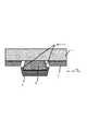
本発明の実施形態での半導体チップの製造方法での途中の状態を半導体ウエハ1の構造を用いて説明したものである。図1の半導体ウエハ1の構造は、図3(C)及び図6(C)の状態と同じものである。なお、本発明で説明する半導体ウエハ1の構造は、半導体ウエハ1を直線に破断した場合の断面図で示している。 The state in the middle of the semiconductor chip manufacturing method according to the embodiment of the present invention is described using the structure of the
なお、便宜的に、図の上面側である半導体ウエハ1上にチップ領域がある面を1A(表面側)とし、裏面電極がある面を1B(裏面側)として以降の説明を行う。
以下、層(膜)ごとに説明する。
半導体ウエハ1(例えばSi基板)の表面には、半導体層2(例えばSi膜)があり、この半導体層2の上面側には、配線形成層3が形成されている。
配線形成層3の中には、絶縁層3A(例えばSiO2膜)及びこの絶縁層3A内で配線部分を構成する金属層3A(例えばCu膜)とで形成されている。
配線形成層3の部分的な表面にはパッシベーション膜4(例えばSiN膜)が露出している。For convenience, the following description will be given assuming that the surface having the chip region on the semiconductor wafer 1 on the upper surface side of the drawing is 1A (front surface side) and the surface having the back electrode is 1B (back surface side).
Hereinafter, each layer (film) will be described.
A semiconductor layer 2 (for example, a Si film) is provided on the surface of the semiconductor wafer 1 (for example, a Si substrate), and a
In the
A passivation film 4 (for example, a SiN film) is exposed on a partial surface of the
さらに、配線形成層3の部分的な表面には、配線形成層3の中の金属層3Bに電気的に接続され、外部配線接続用電極として機能するボンディングパッド部7(例えばAl膜)も形成されている。 Furthermore, a bonding pad portion 7 (for example, an Al film) that is electrically connected to the
半導体ウエハ1の表面側には、平面視した場合に格子状であるダイシングライン部5(分割領域)が設けされている。このダイシングライン部5をダイシングすることで、複数のチップ部6(チップ形成領域)6同士をそれぞれ分断することができる。 On the surface side of the
パッシベーション膜4は、半導体ウエハ1の表面側において、チップ部6のボンディングパット部7とダイシングライン部5とを除く、全て領域を覆うように形成されている。
尚、半導体ウエハ1の表面側のパッシベーション膜4の領域は、ボッシュプロセスでのエッチングプロセスによってもエッチングされることはない。The
Note that the region of the
半導体ウエハ1の裏面側の裏面電極層8は半導体チップを実装する際の電極として用いられ、単層(例えばAu膜)や積層(例えばAl膜/Ti膜/Ni膜/Au膜)の金属膜で形成されている。 The back
このような半導体デバイスウエハをダイシングライン部5において、それぞれのチップ部6を分割することにより、分割された後のチップ部6が個々の半導体デバイスとなる。
図2及び図3を説明する。
図2は、半導体チップの製造方法で必要となる第1の実施形態の各工程をステップ毎に記載したフローチャートである。
図3は、半導体チップの製造方法で必要となる第1の実施形態の各工程をステップ毎に半導体ウエハ1の断面図で記載したものある。
(1)領域形成工程
S101において、図3(A)に示したようなダイシングする前の半導体ウエハ1を準備する。By dividing each of the
2 and 3 will be described.
FIG. 2 is a flowchart describing each step of the first embodiment necessary for the semiconductor chip manufacturing method.
FIG. 3 is a cross-sectional view of the
(1) Region Formation Step In S101, the semiconductor wafer 1 before dicing as shown in FIG.
このように領域形成工程では、露出する面が金属膜7やパッシベーション膜4で被覆されている複数のチップ領域6と、この露出する面にシリコン基板1またはシリコン膜2が露出している複数のチップ領域をそれぞれ分断する分断領域5(ダイシングライン部)とを、シリコン基板の第1の表面上にそれぞれ形成する。
(2)パターンニング工程As described above, in the region forming step, a plurality of
(2) Patterning process
S102において半導体ウエハ1の裏面側にレジストコーター装置10を用いてレジストを塗布する。その後、表面側のダイシングライン部5に対応する裏面側にだけ、レジスト膜が残るように、露光装置11を用いて露光を行い、デベロッパー装置12にてレジスト膜の現像処理を行うことで、図3(B)に示したように裏面側にパターニングされたレジスト膜9を形成する。この時の状態を図7の下図に示す。 In S <b> 102, a resist is applied to the back side of the
なお、裏面側にレジスト膜9をパターンニングするためには、表面側にダイシングライン部5を形成する場合に用いた、露光装置11用のフォトマスクと同じマスクを使用すればよい。 In order to pattern the
このようにパターンニング工程では、複数のチップ領域6が形成されている表面側とは反対面である裏面側上の、分断領域5(ダイシングライン部)のちょうど反対面側に相当する領域に、レジスト膜9が存在するようにパターンニングする。
(3)成膜工程Thus, in the patterning process, on the back surface side that is the surface opposite to the surface side on which the plurality of
(3) Film formation process
S103において、裏面パターニングレジスト9を形成した半導体ウエハ1の裏面上に例えばスパッタリング装置12もしくは真空蒸着装置13にて裏面電極を成膜する。 In S103, a back electrode is formed on the back surface of the
成膜した裏面電極層8は裏面パターニングレジスト9上にも成膜されるが、図3(C)に示したように裏面パターニングレジスト9の側面側の成膜は上面側の成膜と比較して薄くなる。 The formed
ここで成膜工程において、裏面パターニングレジスト9上に裏面電極層8が成膜された状態の裏面パターニングレジスト9近傍の拡大図を図4に示す。具体的には裏面パターニングレジスト9の形状を逆テーパ形状にする事で、裏面パターニングレジスト9の側面側には裏面電極層8があまり成膜されない構造にすることができる。 Here, FIG. 4 shows an enlarged view of the vicinity of the back surface patterning resist 9 in a state where the back
このように成膜工程では、パターンニングされたレジスト膜上を被覆するように電極膜8を成膜して、パターンニングされたレジスト膜9により成膜した電極膜8に段差をつけている。
(4)貼付工程As described above, in the film forming process, the
(4) Pasting process
S104において、図3(D)に示すように、半導体ウエハ1の裏面側をダイシングテープ14に貼り付ける。このように貼付工程では、成膜工程により段差をつけた裏面側をテープに貼り付ける。
(5)エッチング工程In S104, as shown in FIG. 3D, the back side of the
(5) Etching process
S105において、図3(D)のような状態になった半導体ウエハ1の表面側にプラズマを用いたエッチング処理を行う。具体的にはドライエッチング装置にて、装置内の圧力条件およびガス条件などを切り換えてプラズマを発生させることにより、半導体層2(シリコン膜)に対するエッチング処理を実施する。 In S105, an etching process using plasma is performed on the surface side of the
このエッチング工程では、例えばSF6主体のガスを用いてエッチング処理が行われるので、パッシベーション膜4、配線形成層3およびボンディングパッド7がマスクとして機能し、半導体層2(シリコン膜)のエッチング処理が行われる。半導体層2(シリコン膜)のエッチング処理に引き続き、その下のシリコン基板1も深さ方向にエッチング処理が行われる。 In this etching process, for example, an etching process is performed using a gas mainly composed of SF6. Therefore, the
プラズマエッチングによって、図3(E)に示すようにダイシングライン部5の下にあるシリコン基板1の裏面側まで貫通すると、プラズマの発生を停止させてプラズマエッチングを終了させる。 When plasma etching penetrates to the back side of the
第1の実施の形態によれば、例えばSF6主体のガスを用いてエッチング処理を実施するエッチング工程で、エッチングが困難である裏面電極層8をダイシングテープ14に残した状態にする事ができる。
このようにエッチング工程では、表面側から、プラズマエッチング可能な深さまで、シリコン基板1をエッチングする。
(6)除去工程According to the first embodiment, for example, the
Thus, in the etching process, the
(6) Removal process
S106において、図3(E)のような状態になった半導体ウエハ1の表面側にプラズマアッシング装置を用いたアッシング処理を行う。具体的にはドライエッチング装置もしくはアッシング装置にて、装置内の圧力条件およびガス条件などを切り換えてプラズマを発生させることにより、有機膜で裏面パターニングレジストを灰化させることでアッシング処理を実施する。 In S106, an ashing process using a plasma ashing apparatus is performed on the surface side of the
この除去工程では、例えばO2主体のガスを用いてレジストアッシング処理が行われ、図3(F)に示すように裏面パターニングレジスト膜9が除去されると、プラズマの発生を停止させてプラズマアッシングを終了させる。 In this removing step, for example, a resist ashing process is performed using a gas mainly composed of
第1の実施の形態によれば、例えばO2主体のガスを用いてアッシング処理を実施する除去工程で、プラズマエッチングでは分離である複数のチップ領域の間に存在していた裏面電極層8を、ダイシングソーを用いずに分断する事ができる。
さらに、除去工程ではアッシング処理中にボンディングパット7上を付着する、例えばC系の付着物も同時にアッシングする事もできる。According to the first embodiment, for example, the
Further, in the removing step, for example, C-based deposits adhering to the
このように除去工程では、エッチング工程の後に、表面側から、分断領域5(ダイシングライン部)のちょうど反対面側に相当する領域に存在していたレジスト膜を除去する。
(7)剥離工程In this way, in the removing step, after the etching step, the resist film existing in the region corresponding to the opposite side of the dividing region 5 (dicing line portion) is removed from the surface side.
(7) Peeling process
S107において、レジスト膜9を除去した後のシリコン基板1を、ダイスピッカーを用いてテープから剥離する。例えば、ダイシングテープ上に張り付いたチップの剥離を容易にする為に、UV光を照射しテープの粘着性を劣化させた物を、ダイスピッカーにてトレーに整列、収納する。ダイスピッカーは例えばダイシングテープ裏面から押し上げピンを用いて良品チップを持ち上げ、チップ表面から真空吸着法にてチップをピックアップし、トレーに整列、収納する。
図4及び図5を説明する。
図4は、半導体チップの製造方法で必要となる第2の実施形態の各工程をステップ毎に記載したフローチャートである。
図5は、半導体チップの製造方法で必要となる第2の実施形態の各工程をステップ毎に半導体ウエハ1の断面図で記載したものである。In S107, the
4 and 5 will be described.
FIG. 4 is a flowchart describing each step of the second embodiment necessary for the semiconductor chip manufacturing method.
FIG. 5 is a cross-sectional view of the
前述した第1の実施形態では、半導体ウエハ1に対して、表面側よりプラズマを用いたエッチング処理を行ってから裏面パターニングレジストに対するアッシング処理を実施するような場合について説明したが、変形例として、裏面レジストパターニングに対するアッシング処理を行ってから半導体ウエハ1に対して、表面側よりプラズマを用いたエッチング処理を行ってもよく、図4及び図5及び図6を用いて説明する。
(1)領域形成工程
S201において、図5(A)に示したようなダイシングする前の半導体ウエハ1を準備する。In the first embodiment described above, the case where the
(1) Region Formation Step In S201, the
このように領域形成工程では、露出する面が金属膜7やパッシベーション膜4で被覆されている複数のチップ領域6と、この露出する面にシリコン基板1またはシリコン膜2が露出している複数のチップ領域をそれぞれ分断する分断領域5(ダイシングライン部)とを、シリコン基板の第1の表面上にそれぞれ形成する。
(2)パターンニング工程As described above, in the region forming step, a plurality of
(2) Patterning process
S202において半導体ウエハ1の裏面側にレジストコーター装置10を用いてレジストを塗布する。その後、表面側のダイシングライン部5に対応する裏面側にだけ、レジスト膜が残るように、露光装置11を用いて露光を行い、デベロッパー装置12にてレジスト膜の現像処理を行うことで、図5(B)に示したように裏面側にパターニングされたレジスト膜9を形成する。この時の状態を図7の下図に示す。 In S <b> 202, a resist is applied to the back side of the
なお、裏面側にレジスト膜9をパターンニングするためには、表面側にダイシングライン部5を形成する場合に用いた、露光装置11用のフォトマスクと同じマスクを使用すればよい。 In order to pattern the resist
このようにパターンニング工程では、複数のチップ領域6が形成されている表面側とは反対面である裏面側上の、分断領域5(ダイシングライン部)のちょうど反対面側に相当する領域に、レジスト膜9が存在するようにパターンニングする。
(3)成膜工程Thus, in the patterning process, on the back surface side that is the surface opposite to the surface side on which the plurality of
(3) Film formation process
S203において、裏面パターニングレジスト9を形成した半導体ウエハ1の裏面上に例えばスパッタリング装置12もしくは真空蒸着装置13にて裏面電極を成膜する。
ここで成膜工程において、裏面パターニングレジスト9上に裏面電極層8が成膜された状態の裏面パターニングレジスト9近傍の拡大図を図6に示す。In S <b> 203, a back electrode is formed on the back surface of the
FIG. 6 shows an enlarged view of the vicinity of the back surface patterning resist 9 in a state where the back
具体的には裏面パターニングレジスト9の形状を逆テーパ形状にする事で、裏面パターニングレジスト9の側面側には裏面電極層8が形成されない構造にすることができる。
(4)除去工程Specifically, by making the shape of the back surface patterning resist 9 into a reverse taper shape, a structure in which the back
(4) Removal process
S204において、図5(C)のような状態になった半導体ウエハ1の裏面側を例えばウエットアッシング装置を用いたアッシング処理を行う。このアッシング工程では、例えば硫酸加水やアンモニア加水を用いたアッシング処理を実施すると、逆テーパ形状に形成された裏面パターニングレジスト9の側面から液体が侵入し裏面パターニングレジスト9が溶解すると同時に裏面パターニングレジスト上に成膜された金属膜が除去される。この技術はピールオフとよばれる。 In S204, an ashing process using, for example, a wet ashing apparatus is performed on the back side of the
このように裏面パターンレジスト除去工程では、エッチング工程の前に、裏面側から、分断領域5(ダイシングライン部)のちょうど反対面側に相当する領域に存在していたレジスト膜とその上に生成した裏面電極層同時に除去し、図5(D)のサンプルが完成される。
(5)貼付工程As described above, in the back surface pattern resist removing step, the resist film was formed on the resist film that existed in the region corresponding to the opposite surface side of the dividing region 5 (dicing line portion) from the back surface side before the etching step. The back electrode layer is removed simultaneously to complete the sample shown in FIG.
(5) Pasting process
S205において、図5(E)に示すように、半導体ウエハ1の裏面側をダイシングテープ14に貼り付ける。このように貼付工程では、除去工程により、レジスト膜を除去した裏面側をテープに貼り付ける。
(6)エッチング工程In S205, as shown in FIG. 5E, the back side of the
(6) Etching process
S206において、図5(E)のような状態になった半導体ウエハ1の表面側にプラズマを用いたエッチング処理を行う。具体的にはドライエッチング装置にて、装置内の圧力条件およびガス条件などを切り換えてプラズマを発生させることにより、半導体層2(シリコン膜)に対するエッチング処理を実施する。 In S206, an etching process using plasma is performed on the surface side of the
このエッチング工程では、例えばSF6主体のガスを用いてエッチング処理が行われるので、パッシベーション膜4、配線形成層3およびボンディングパッド7がマスクとして機能し、半導体層2(シリコン膜)のエッチング処理が行われる。半導体層2(シリコン膜)のエッチング処理に引き続き、その下のシリコン基板1も深さ方向にエッチング処理が行われる。 In this etching process, for example, an etching process is performed using a gas mainly composed of SF6. Therefore, the
プラズマエッチングによって、図5(F)に示すようにダイシングライン部5の下にあるシリコン基板1の裏面側まで貫通すると、プラズマの発生を停止させてプラズマエッチングを終了させる。 When plasma etching penetrates to the back side of the
第2の実施の形態によれば、例えばSF6主体のガスを用いてエッチング処理を実施するエッチング工程で、エッチングが困難である裏面電極層8が存在しない状態で、ダイシング部5を分断する事ができる。
このようにエッチング工程では、表面側から、プラズマエッチング可能な深さまで、シリコン基板1をエッチングする。
(7)剥離工程According to the second embodiment, for example, in the etching process in which the etching process is performed using a gas mainly composed of SF6, the dicing
Thus, in the etching process, the
(7) Peeling process
S207において、レジスト膜9を除去した後のシリコン基板1を、ダイスピッカーを用いてテープから剥離する。例えば、ダイシングテープ上に張り付いたチップの剥離を容易にする為に、UV光を照射しテープの粘着性を劣化させた物を、ダイスピッカーにてトレーに整列、収納する。ダイスピッカーは例えばダイシングテープ裏面から押し上げピンを用いて良品チップを持ち上げ、チップ表面から真空吸着法にてチップをピックアップし、トレーに整列、収納する。 In S207, the
1 シリコン基板(半導体ウエハ)
1A 基板の表面側
1B 基板の裏面側
2 半導体層(シリコン膜)
3 配線形成層
3A 絶縁層
3B 金属層
4 パッシベーション膜
5 ダイシングライン部(分離領域)
6 チップ部(チップ領域)
7 ボンディングパッド部
8 裏面電極層(金属膜)
9 裏面パターニングレジスト(フォトレジスト膜)
10 レジストコーター
11 露光装置
12 デベロッパー
12 スパッタリング装置
13 真空蒸着装置
14 ダイシングテープ1 Silicon substrate (semiconductor wafer)
1A Front side of
3 Wiring forming
6 Chip part (chip area)
7
9 Back side patterning resist (photoresist film)
DESCRIPTION OF SYMBOLS 10 Resist coater 11 Exposure apparatus 12 Developer 12 Sputtering apparatus 13
Claims (5)
Translated fromJapanese前記複数のチップ領域が形成されている前記第1の表面とは反対面である第2の表面上の、前記第1の領域の反対面側に相当する第2の領域にレジスト膜が存在するようにパターンニングするパターンニング工程と、
前記パターンニングされたレジスト膜上を被覆するように電極膜を成膜して、前記パターンニングされたレジスト膜により前記成膜した電極膜に段差をつける成膜工程と、
前記第1の表面側から、プラズマエッチング可能な深さまで、前記シリコン基板をエッチングするエッチング工程と、
前記エッチング工程の後に、前記第1の表面側から、前記第2の領域に存在するレジスト膜を除去する除去工程と、
を含むことを特徴とする半導体チップの製造方法。A plurality of chip regions whose exposed surfaces are covered with a metal film, and a first region that divides each of the plurality of chip regions where the silicon substrate or the silicon film is exposed on the exposed surface are formed on the silicon substrate. A region forming step for forming each on the first surface;
A resist film is present in a second region corresponding to the surface opposite to the first region on the second surface opposite to the first surface on which the plurality of chip regions are formed. Patterning process to pattern,
A film forming step of forming an electrode film so as to cover the patterned resist film, and forming a step on the formed electrode film by the patterned resist film;
An etching step of etching the silicon substrate from the first surface side to a depth capable of plasma etching;
After the etching step, a removal step of removing the resist film present in the second region from the first surface side;
A method for manufacturing a semiconductor chip, comprising:
前記レジスト膜を除去した後の前記シリコン基板を、テープから剥離する剥離工程と、
をさらに含むことを特徴とする請求項に記載の半導体チップの製造方法。An attaching step of attaching the second surface side with a step by the film forming step to the tape;
A peeling step of peeling the silicon substrate after removing the resist film from the tape;
The method of manufacturing a semiconductor chip according to claim 1, further comprising:
前記複数のチップ領域が形成されている前記第1の表面とは反対面である第2の表面上の、前記第1の領域の反対面側に相当する第2の領域にレジスト膜が存在するようにパターンニングするパターンニング工程と、
前記パターンニングされたレジスト膜上を被覆するように電極膜を成膜して、前記パターンニングされたレジスト膜により前記成膜した電極膜に段差をつける成膜工程と、
前記第2の表面側から、前記第2の領域に存在する電極膜及びレジスト膜を除去する除去工程と、
前記除去工程の後に、前記第1の表面側から、プラズマエッチング可能な深さまで、前記シリコン基板をエッチングするエッチング工程と、
を含むことを特徴とする半導体チップの製造方法。A plurality of chip regions whose exposed surfaces are covered with a metal film, and a first region that divides each of the plurality of chip regions where the silicon substrate or the silicon film is exposed on the exposed surface are formed on the silicon substrate. A region forming step for forming each on the first surface;
A resist film is present in a second region corresponding to the surface opposite to the first region on the second surface opposite to the first surface on which the plurality of chip regions are formed. Patterning process to pattern,
A film forming step of forming an electrode film so as to cover the patterned resist film, and forming a step on the formed electrode film by the patterned resist film;
A removing step of removing the electrode film and the resist film existing in the second region from the second surface side;
After the removing step, an etching step of etching the silicon substrate from the first surface side to a depth capable of plasma etching;
A method for manufacturing a semiconductor chip, comprising:
前記エッチングした後の前記シリコン基板を、テープから剥離する剥離工程と、
をさらに含むことを特徴とする請求項3に記載の半導体チップの製造方法。An attaching step of attaching the second surface side from which the resist film has been removed to the tape;
A peeling step of peeling the silicon substrate after the etching from the tape;
The method of manufacturing a semiconductor chip according to claim 3, further comprising:
5. The resist film according to claim 1, wherein in the patterning step, the resist film is patterned in the second region so as to have an inversely tapered shape. 6. Semiconductor chip manufacturing method.
Priority Applications (1)
| Application Number | Priority Date | Filing Date | Title |
|---|---|---|---|
| JP2015129211AJP6582616B2 (en) | 2015-06-26 | 2015-06-26 | Manufacturing method of semiconductor chip |
Applications Claiming Priority (1)
| Application Number | Priority Date | Filing Date | Title |
|---|---|---|---|
| JP2015129211AJP6582616B2 (en) | 2015-06-26 | 2015-06-26 | Manufacturing method of semiconductor chip |
Publications (3)
| Publication Number | Publication Date |
|---|---|
| JP2017017072Atrue JP2017017072A (en) | 2017-01-19 |
| JP2017017072A5 JP2017017072A5 (en) | 2018-09-13 |
| JP6582616B2 JP6582616B2 (en) | 2019-10-02 |
Family
ID=57831009
Family Applications (1)
| Application Number | Title | Priority Date | Filing Date |
|---|---|---|---|
| JP2015129211AActiveJP6582616B2 (en) | 2015-06-26 | 2015-06-26 | Manufacturing method of semiconductor chip |
Country Status (1)
| Country | Link |
|---|---|
| JP (1) | JP6582616B2 (en) |
Cited By (3)
| Publication number | Priority date | Publication date | Assignee | Title |
|---|---|---|---|---|
| WO2018142976A1 (en)* | 2017-02-01 | 2018-08-09 | 株式会社村田製作所 | Csp-type semiconductor device and method for manufacturing same |
| JP2018186240A (en)* | 2017-04-27 | 2018-11-22 | 株式会社東芝 | Manufacturing method of semiconductor device |
| JP2020013059A (en)* | 2018-07-20 | 2020-01-23 | 株式会社東芝 | Device manufacturing method |
Citations (4)
| Publication number | Priority date | Publication date | Assignee | Title |
|---|---|---|---|---|
| JPS61287241A (en)* | 1985-06-14 | 1986-12-17 | Sharp Corp | Manufacture of semiconductor element |
| JPH08120443A (en)* | 1994-10-21 | 1996-05-14 | Fuji Elelctrochem Co Ltd | Film pattern formation method by lift-off |
| JP2002093749A (en)* | 2000-06-27 | 2002-03-29 | Robert Bosch Gmbh | Method for dividing substrate wafer into a plurality of substrate chips |
| JP2002184698A (en)* | 2000-12-18 | 2002-06-28 | Murata Mfg Co Ltd | Method of manufacturing electronic component |
- 2015
- 2015-06-26JPJP2015129211Apatent/JP6582616B2/enactiveActive
Patent Citations (4)
| Publication number | Priority date | Publication date | Assignee | Title |
|---|---|---|---|---|
| JPS61287241A (en)* | 1985-06-14 | 1986-12-17 | Sharp Corp | Manufacture of semiconductor element |
| JPH08120443A (en)* | 1994-10-21 | 1996-05-14 | Fuji Elelctrochem Co Ltd | Film pattern formation method by lift-off |
| JP2002093749A (en)* | 2000-06-27 | 2002-03-29 | Robert Bosch Gmbh | Method for dividing substrate wafer into a plurality of substrate chips |
| JP2002184698A (en)* | 2000-12-18 | 2002-06-28 | Murata Mfg Co Ltd | Method of manufacturing electronic component |
Cited By (4)
| Publication number | Priority date | Publication date | Assignee | Title |
|---|---|---|---|---|
| WO2018142976A1 (en)* | 2017-02-01 | 2018-08-09 | 株式会社村田製作所 | Csp-type semiconductor device and method for manufacturing same |
| JP6424996B1 (en)* | 2017-02-01 | 2018-11-21 | 株式会社村田製作所 | CSP type semiconductor device and method of manufacturing the same |
| JP2018186240A (en)* | 2017-04-27 | 2018-11-22 | 株式会社東芝 | Manufacturing method of semiconductor device |
| JP2020013059A (en)* | 2018-07-20 | 2020-01-23 | 株式会社東芝 | Device manufacturing method |
Also Published As
| Publication number | Publication date |
|---|---|
| JP6582616B2 (en) | 2019-10-02 |
Similar Documents
| Publication | Publication Date | Title |
|---|---|---|
| CN100448043C (en) | Manufacturing method of light emitting device | |
| US9969609B2 (en) | MEMS device | |
| KR101585554B1 (en) | Embedded trace substrate and method manufacturing bump of the same | |
| US20060205182A1 (en) | Method for manufacturing semiconductor device | |
| CN104952794B (en) | Prepare for the section of back metal | |
| US9754832B2 (en) | Semiconductor wafer and method of producing the same | |
| US20140252571A1 (en) | Wafer-level package mitigated undercut | |
| US9064950B2 (en) | Fabrication method for a chip package | |
| US10685883B1 (en) | Method of wafer dicing and die | |
| CN111129253A (en) | Flip-chip microelectronic device structure and fabrication method thereof | |
| KR101784655B1 (en) | Semiconductor device and method | |
| US20200075482A1 (en) | Semiconductor device and manufacturing method thereof | |
| US20150235856A1 (en) | Semiconductor structures having t-shaped electrodes | |
| US20200168464A1 (en) | Method for removing a sacrificial layer on semiconductor wafers | |
| CN110931428A (en) | Method for dividing multiple semiconductor tube cores | |
| JP6582616B2 (en) | Manufacturing method of semiconductor chip | |
| JP2008218832A (en) | Semiconductor device and manufacturing method thereof | |
| JP5228381B2 (en) | Manufacturing method of semiconductor device | |
| JP5568824B2 (en) | Manufacturing method of semiconductor device | |
| US9633902B2 (en) | Method for manufacturing semiconductor device that includes dividing semiconductor substrate by dry etching | |
| JP4703127B2 (en) | Semiconductor wafer, semiconductor chip and manufacturing method thereof | |
| JP2016167574A (en) | Method of manufacturing semiconductor device | |
| JPH10312980A (en) | Manufacture of semiconductor device | |
| JP2004349550A (en) | Semiconductor device and manufacturing method thereof | |
| CN102097428A (en) | Integrated circuit wafer and integrated circuit wafer cutting method |
Legal Events
| Date | Code | Title | Description |
|---|---|---|---|
| RD03 | Notification of appointment of power of attorney | Free format text:JAPANESE INTERMEDIATE CODE: A7423 Effective date:20161101 | |
| RD04 | Notification of resignation of power of attorney | Free format text:JAPANESE INTERMEDIATE CODE: A7424 Effective date:20161101 | |
| A621 | Written request for application examination | Free format text:JAPANESE INTERMEDIATE CODE: A621 Effective date:20180626 | |
| RD03 | Notification of appointment of power of attorney | Free format text:JAPANESE INTERMEDIATE CODE: A7423 Effective date:20180703 | |
| A521 | Request for written amendment filed | Free format text:JAPANESE INTERMEDIATE CODE: A523 Effective date:20180730 | |
| RD04 | Notification of resignation of power of attorney | Free format text:JAPANESE INTERMEDIATE CODE: A7424 Effective date:20181031 | |
| RD04 | Notification of resignation of power of attorney | Free format text:JAPANESE INTERMEDIATE CODE: A7424 Effective date:20190109 | |
| A131 | Notification of reasons for refusal | Free format text:JAPANESE INTERMEDIATE CODE: A131 Effective date:20190212 | |
| A977 | Report on retrieval | Free format text:JAPANESE INTERMEDIATE CODE: A971007 Effective date:20190214 | |
| A521 | Request for written amendment filed | Free format text:JAPANESE INTERMEDIATE CODE: A523 Effective date:20190412 | |
| TRDD | Decision of grant or rejection written | ||
| A01 | Written decision to grant a patent or to grant a registration (utility model) | Free format text:JAPANESE INTERMEDIATE CODE: A01 Effective date:20190806 | |
| A61 | First payment of annual fees (during grant procedure) | Free format text:JAPANESE INTERMEDIATE CODE: A61 Effective date:20190819 | |
| R151 | Written notification of patent or utility model registration | Ref document number:6582616 Country of ref document:JP Free format text:JAPANESE INTERMEDIATE CODE: R151 | |
| R250 | Receipt of annual fees | Free format text:JAPANESE INTERMEDIATE CODE: R250 | |
| R250 | Receipt of annual fees | Free format text:JAPANESE INTERMEDIATE CODE: R250 | |
| R250 | Receipt of annual fees | Free format text:JAPANESE INTERMEDIATE CODE: R250 | |
| R250 | Receipt of annual fees | Free format text:JAPANESE INTERMEDIATE CODE: R250 |