JP2017009637A - Liquid crystal display - Google Patents
Liquid crystal displayDownload PDFInfo
- Publication number
- JP2017009637A JP2017009637AJP2015121703AJP2015121703AJP2017009637AJP 2017009637 AJP2017009637 AJP 2017009637AJP 2015121703 AJP2015121703 AJP 2015121703AJP 2015121703 AJP2015121703 AJP 2015121703AJP 2017009637 AJP2017009637 AJP 2017009637A
- Authority
- JP
- Japan
- Prior art keywords
- liquid crystal
- ito
- tft substrate
- crystal display
- display device
- Prior art date
- Legal status (The legal status is an assumption and is not a legal conclusion. Google has not performed a legal analysis and makes no representation as to the accuracy of the status listed.)
- Pending
Links
Images


Classifications
- G—PHYSICS
- G02—OPTICS
- G02F—OPTICAL DEVICES OR ARRANGEMENTS FOR THE CONTROL OF LIGHT BY MODIFICATION OF THE OPTICAL PROPERTIES OF THE MEDIA OF THE ELEMENTS INVOLVED THEREIN; NON-LINEAR OPTICS; FREQUENCY-CHANGING OF LIGHT; OPTICAL LOGIC ELEMENTS; OPTICAL ANALOGUE/DIGITAL CONVERTERS
- G02F1/00—Devices or arrangements for the control of the intensity, colour, phase, polarisation or direction of light arriving from an independent light source, e.g. switching, gating or modulating; Non-linear optics
- G02F1/01—Devices or arrangements for the control of the intensity, colour, phase, polarisation or direction of light arriving from an independent light source, e.g. switching, gating or modulating; Non-linear optics for the control of the intensity, phase, polarisation or colour
- G02F1/13—Devices or arrangements for the control of the intensity, colour, phase, polarisation or direction of light arriving from an independent light source, e.g. switching, gating or modulating; Non-linear optics for the control of the intensity, phase, polarisation or colour based on liquid crystals, e.g. single liquid crystal display cells
- G02F1/133—Constructional arrangements; Operation of liquid crystal cells; Circuit arrangements
- G02F1/1333—Constructional arrangements; Manufacturing methods
- G02F1/1339—Gaskets; Spacers; Sealing of cells
- G—PHYSICS
- G02—OPTICS
- G02F—OPTICAL DEVICES OR ARRANGEMENTS FOR THE CONTROL OF LIGHT BY MODIFICATION OF THE OPTICAL PROPERTIES OF THE MEDIA OF THE ELEMENTS INVOLVED THEREIN; NON-LINEAR OPTICS; FREQUENCY-CHANGING OF LIGHT; OPTICAL LOGIC ELEMENTS; OPTICAL ANALOGUE/DIGITAL CONVERTERS
- G02F1/00—Devices or arrangements for the control of the intensity, colour, phase, polarisation or direction of light arriving from an independent light source, e.g. switching, gating or modulating; Non-linear optics
- G02F1/01—Devices or arrangements for the control of the intensity, colour, phase, polarisation or direction of light arriving from an independent light source, e.g. switching, gating or modulating; Non-linear optics for the control of the intensity, phase, polarisation or colour
- G02F1/13—Devices or arrangements for the control of the intensity, colour, phase, polarisation or direction of light arriving from an independent light source, e.g. switching, gating or modulating; Non-linear optics for the control of the intensity, phase, polarisation or colour based on liquid crystals, e.g. single liquid crystal display cells
- G02F1/133—Constructional arrangements; Operation of liquid crystal cells; Circuit arrangements
- G02F1/1333—Constructional arrangements; Manufacturing methods
- G02F1/133345—Insulating layers
- G—PHYSICS
- G02—OPTICS
- G02F—OPTICAL DEVICES OR ARRANGEMENTS FOR THE CONTROL OF LIGHT BY MODIFICATION OF THE OPTICAL PROPERTIES OF THE MEDIA OF THE ELEMENTS INVOLVED THEREIN; NON-LINEAR OPTICS; FREQUENCY-CHANGING OF LIGHT; OPTICAL LOGIC ELEMENTS; OPTICAL ANALOGUE/DIGITAL CONVERTERS
- G02F1/00—Devices or arrangements for the control of the intensity, colour, phase, polarisation or direction of light arriving from an independent light source, e.g. switching, gating or modulating; Non-linear optics
- G02F1/01—Devices or arrangements for the control of the intensity, colour, phase, polarisation or direction of light arriving from an independent light source, e.g. switching, gating or modulating; Non-linear optics for the control of the intensity, phase, polarisation or colour
- G02F1/13—Devices or arrangements for the control of the intensity, colour, phase, polarisation or direction of light arriving from an independent light source, e.g. switching, gating or modulating; Non-linear optics for the control of the intensity, phase, polarisation or colour based on liquid crystals, e.g. single liquid crystal display cells
- G02F1/133—Constructional arrangements; Operation of liquid crystal cells; Circuit arrangements
- G02F1/136—Liquid crystal cells structurally associated with a semi-conducting layer or substrate, e.g. cells forming part of an integrated circuit
- G02F1/1362—Active matrix addressed cells
- G02F1/136204—Arrangements to prevent high voltage or static electricity failures
- G—PHYSICS
- G02—OPTICS
- G02F—OPTICAL DEVICES OR ARRANGEMENTS FOR THE CONTROL OF LIGHT BY MODIFICATION OF THE OPTICAL PROPERTIES OF THE MEDIA OF THE ELEMENTS INVOLVED THEREIN; NON-LINEAR OPTICS; FREQUENCY-CHANGING OF LIGHT; OPTICAL LOGIC ELEMENTS; OPTICAL ANALOGUE/DIGITAL CONVERTERS
- G02F1/00—Devices or arrangements for the control of the intensity, colour, phase, polarisation or direction of light arriving from an independent light source, e.g. switching, gating or modulating; Non-linear optics
- G02F1/01—Devices or arrangements for the control of the intensity, colour, phase, polarisation or direction of light arriving from an independent light source, e.g. switching, gating or modulating; Non-linear optics for the control of the intensity, phase, polarisation or colour
- G02F1/13—Devices or arrangements for the control of the intensity, colour, phase, polarisation or direction of light arriving from an independent light source, e.g. switching, gating or modulating; Non-linear optics for the control of the intensity, phase, polarisation or colour based on liquid crystals, e.g. single liquid crystal display cells
- G02F1/133—Constructional arrangements; Operation of liquid crystal cells; Circuit arrangements
- G02F1/1333—Constructional arrangements; Manufacturing methods
- G02F1/133388—Constructional arrangements; Manufacturing methods with constructional differences between the display region and the peripheral region
- G—PHYSICS
- G02—OPTICS
- G02F—OPTICAL DEVICES OR ARRANGEMENTS FOR THE CONTROL OF LIGHT BY MODIFICATION OF THE OPTICAL PROPERTIES OF THE MEDIA OF THE ELEMENTS INVOLVED THEREIN; NON-LINEAR OPTICS; FREQUENCY-CHANGING OF LIGHT; OPTICAL LOGIC ELEMENTS; OPTICAL ANALOGUE/DIGITAL CONVERTERS
- G02F1/00—Devices or arrangements for the control of the intensity, colour, phase, polarisation or direction of light arriving from an independent light source, e.g. switching, gating or modulating; Non-linear optics
- G02F1/01—Devices or arrangements for the control of the intensity, colour, phase, polarisation or direction of light arriving from an independent light source, e.g. switching, gating or modulating; Non-linear optics for the control of the intensity, phase, polarisation or colour
- G02F1/13—Devices or arrangements for the control of the intensity, colour, phase, polarisation or direction of light arriving from an independent light source, e.g. switching, gating or modulating; Non-linear optics for the control of the intensity, phase, polarisation or colour based on liquid crystals, e.g. single liquid crystal display cells
- G02F1/133—Constructional arrangements; Operation of liquid crystal cells; Circuit arrangements
- G02F1/1333—Constructional arrangements; Manufacturing methods
- G02F1/1337—Surface-induced orientation of the liquid crystal molecules, e.g. by alignment layers
- G—PHYSICS
- G02—OPTICS
- G02F—OPTICAL DEVICES OR ARRANGEMENTS FOR THE CONTROL OF LIGHT BY MODIFICATION OF THE OPTICAL PROPERTIES OF THE MEDIA OF THE ELEMENTS INVOLVED THEREIN; NON-LINEAR OPTICS; FREQUENCY-CHANGING OF LIGHT; OPTICAL LOGIC ELEMENTS; OPTICAL ANALOGUE/DIGITAL CONVERTERS
- G02F1/00—Devices or arrangements for the control of the intensity, colour, phase, polarisation or direction of light arriving from an independent light source, e.g. switching, gating or modulating; Non-linear optics
- G02F1/01—Devices or arrangements for the control of the intensity, colour, phase, polarisation or direction of light arriving from an independent light source, e.g. switching, gating or modulating; Non-linear optics for the control of the intensity, phase, polarisation or colour
- G02F1/13—Devices or arrangements for the control of the intensity, colour, phase, polarisation or direction of light arriving from an independent light source, e.g. switching, gating or modulating; Non-linear optics for the control of the intensity, phase, polarisation or colour based on liquid crystals, e.g. single liquid crystal display cells
- G02F1/133—Constructional arrangements; Operation of liquid crystal cells; Circuit arrangements
- G02F1/136—Liquid crystal cells structurally associated with a semi-conducting layer or substrate, e.g. cells forming part of an integrated circuit
- G02F1/1362—Active matrix addressed cells
- G02F1/136218—Shield electrodes
- G—PHYSICS
- G02—OPTICS
- G02F—OPTICAL DEVICES OR ARRANGEMENTS FOR THE CONTROL OF LIGHT BY MODIFICATION OF THE OPTICAL PROPERTIES OF THE MEDIA OF THE ELEMENTS INVOLVED THEREIN; NON-LINEAR OPTICS; FREQUENCY-CHANGING OF LIGHT; OPTICAL LOGIC ELEMENTS; OPTICAL ANALOGUE/DIGITAL CONVERTERS
- G02F2202/00—Materials and properties
- G02F2202/22—Antistatic materials or arrangements
Landscapes
- Physics & Mathematics (AREA)
- Nonlinear Science (AREA)
- Mathematical Physics (AREA)
- Chemical & Material Sciences (AREA)
- Crystallography & Structural Chemistry (AREA)
- General Physics & Mathematics (AREA)
- Optics & Photonics (AREA)
- Engineering & Computer Science (AREA)
- Microelectronics & Electronic Packaging (AREA)
- Liquid Crystal (AREA)
- Spectroscopy & Molecular Physics (AREA)
- Geometry (AREA)
Abstract
Description
Translated fromJapanese本発明は表示装置に係り、狭額縁としても、シール部の信頼性を確保出来る液晶表示装置に関する。 The present invention relates to a display device, and more particularly, to a liquid crystal display device that can ensure the reliability of a seal portion even with a narrow frame.
液晶表示装置では画素電極および薄膜トランジスタ(TFT)等を有する画素がマトリクス状に形成されたTFT基板と、TFT基板に対向して対向基板が配置され、TFT基板と対向基板の間に液晶が挟持されている構成となっている。そして液晶分子による光の透過率を画素毎に制御することによって画像を形成している。 In a liquid crystal display device, a TFT substrate in which pixels having pixel electrodes and thin film transistors (TFTs) are formed in a matrix and a counter substrate are arranged opposite the TFT substrate, and liquid crystal is sandwiched between the TFT substrate and the counter substrate. It has become the composition. An image is formed by controlling the light transmittance of the liquid crystal molecules for each pixel.
中小型の液晶表示パネルでは、外形を小さく保ったまま、表示領域を大きくしたいという要求が強い。そうすると、表示領域の端部から液晶表示パネルの端部までの幅が小さくなり、いわゆる狭額縁となる。狭額縁では、TFT基板と対向基板を接着しているシール材のシール幅が小さくなり、シール部の接着力が問題となる。 In the small-sized liquid crystal display panel, there is a strong demand to increase the display area while keeping the outer shape small. As a result, the width from the end of the display area to the end of the liquid crystal display panel is reduced, resulting in a so-called narrow frame. In the narrow frame, the sealing width of the sealing material that bonds the TFT substrate and the counter substrate becomes small, and the adhesive force of the sealing portion becomes a problem.
TFT基板と対向基板が液晶と接する面には、液晶を初期配向させるために配向膜が形成されている。従来は、シール部における接着力の信頼性を向上させるために、シール部には配向膜を形成しないような構成がとられてきた。しかし、狭額縁となると、配向膜をシール部から排除することが難しくなる。したがって、シール部における接着の信頼性を考える場合は、シール材と配向膜の接着強度、配向膜とその下地膜との接着強度を考える必要がある。 On the surface where the TFT substrate and the counter substrate are in contact with the liquid crystal, an alignment film is formed for initial alignment of the liquid crystal. Conventionally, in order to improve the reliability of the adhesive force in the seal portion, a configuration has been adopted in which an alignment film is not formed on the seal portion. However, when the frame is narrow, it becomes difficult to remove the alignment film from the seal portion. Therefore, when considering the reliability of the adhesion at the seal portion, it is necessary to consider the adhesion strength between the sealing material and the alignment film and the adhesion strength between the alignment film and the underlying film.
特許文献1には、表示領域において、配線によって凸部ができた部分の上の配向膜がラビングで剥離することを防止するために、凸部にITO(Indiun Tin Oxide)を配置して、配向膜の接着強度を上げることが記載されている。また、特許文献2には、ITOによって配線を形成し、このITO配線をシール部の下を通過して端子領域に延在させる構成が記載されている。特許文献2には、配向膜の塗布範囲については記載が無い。 In Patent Document 1, in order to prevent the alignment film on the portion where the convex portion is formed by the wiring in the display area from being peeled off by rubbing, ITO (Indian Tin Oxide) is arranged on the convex portion to align the alignment layer. It describes increasing the adhesive strength of the film. Patent Document 2 describes a configuration in which a wiring is formed of ITO, and this ITO wiring passes under the seal portion and extends to the terminal region. Patent Document 2 does not describe the application range of the alignment film.
シール部の信頼性について、従来は、シール材と配向膜の接着力のみに関心が払われてきた。しかし、シール材と配向膜の接着力が向上すると、配向膜とその下地膜の接着が問題となる。従来は、配向膜と下地膜は十分な接着強度があると考えられてきたが、狭額縁となるにしたがって、配向膜とその下地膜との接着力が問題となってきたのである。 Regarding the reliability of the seal portion, conventionally, attention has been paid only to the adhesive force between the seal material and the alignment film. However, when the adhesive force between the sealing material and the alignment film is improved, the adhesion between the alignment film and the base film becomes a problem. Conventionally, it has been considered that the alignment film and the base film have sufficient adhesive strength. However, the adhesive force between the alignment film and the base film has become a problem as the frame becomes narrower.
配向膜の下地膜は、TFT基板側と対向基板側とでは異なる。対向基板側は、オーバーコート膜という有機膜が下地膜になっているのに対し、TFT基板側ではSiNx等の無機絶縁膜が下地膜となっている場合が多い。配向膜はポリイミド等で形成された有機膜である。一般に、有機膜と有機膜の接着強度は強いが、有機膜と無機膜の接着強度は比較的弱い。したがって、配向膜と下地膜の接着力は、TFT基板側で問題となる。 The base film of the alignment film is different between the TFT substrate side and the counter substrate side. On the counter substrate side, an organic film called an overcoat film is a base film, whereas on the TFT substrate side, an inorganic insulating film such as SiNx is often the base film. The alignment film is an organic film formed of polyimide or the like. In general, the adhesive strength between the organic film and the organic film is strong, but the adhesive strength between the organic film and the inorganic film is relatively weak. Therefore, the adhesive force between the alignment film and the base film becomes a problem on the TFT substrate side.
本発明の課題は、配向膜と下地膜との接着強度を上げ、狭額縁としても、シール部の信頼性を確保した液晶表示装置を実現することである。 An object of the present invention is to realize a liquid crystal display device in which the adhesion strength between an alignment film and a base film is increased and the reliability of a seal portion is ensured even with a narrow frame.
本発明は上記問題を克服するものであり、代表的な手段は次のとおりである。すなわち、画素がマトリクス状に形成され、配向膜を有し、外形が矩形であるTFT基板と、外形が矩形である対向基板がシール部においてシール材によって接着し、内部に液晶が封入された液晶表示装置であって、前記TFT基板は表示領域と端子領域を有し、前記表示領域は、前記シール材に囲まれた領域に形成され、前記対向基板は前記端子領域には存在しておらず、前記TFT基板において、前記シール材の下層には配向膜が存在し、前記配向膜の下層には酸化物導電膜が存在し、前記酸化物導電膜は、前記TFT基板の端部にまで形成され、前記酸化物導電膜はフロートであることを特徴とする液晶表示装置である。 The present invention overcomes the above problems, and typical means are as follows. That is, a liquid crystal in which pixels are formed in a matrix, an alignment film is provided, a TFT substrate having a rectangular outer shape, and a counter substrate having a rectangular outer shape are bonded to each other by a sealing material at a seal portion, and liquid crystal is sealed inside In the display device, the TFT substrate has a display region and a terminal region, the display region is formed in a region surrounded by the sealing material, and the counter substrate does not exist in the terminal region. In the TFT substrate, an alignment film is present under the sealing material, an oxide conductive film is present under the alignment film, and the oxide conductive film is formed up to the end of the TFT substrate. In the liquid crystal display device, the oxide conductive film is a float.
以下に実施例にしたがって、本発明を詳細に説明する。 Hereinafter, the present invention will be described in detail according to examples.
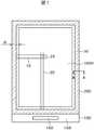
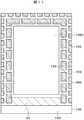
図1は本発明が適用される液晶表示パネルの平面図である。図1において、TFT基板100と対向基板200がシール材30によって接着し、TFT基板100と対向基板200の間に液晶が挟持されている。TFT基板100は対向基板200よりも大きく形成されており、TFT基板100が1枚となっている部分は端子領域150となっている。端子領域150には、液晶表示パネルを駆動するICドライバ160、液晶表示パネルに、電源、映像信号、走査信号等を供給するためのフレキシブル配線基板を接続するための端子等が形成されている。 FIG. 1 is a plan view of a liquid crystal display panel to which the present invention is applied. In FIG. 1, the
図1において、表示領域1000には走査線10が横方向に延在し、縦方向に配列している。また、映像信号線20が縦方向に延在し、横方向に配列している。走査線10と映像信号線20とで囲まれた領域が画素25となっている。狭額縁では、表示領域1000の端部と液晶表示装置の端部の距離dは1mm程度にまで小さくなっている。この場合、シール材30の接着幅は0.4mm程度しか確保することが出来ない。したがって、シール部における接着強度は重要な問題となる。 In FIG. 1,
液晶表示装置は視野角特性が問題である。IPS(In Plane Swiching)方式は、液晶分子をTFT基板の主面と平行方向に回転させることによって透過率を制御するものであり、優れた視野角特性を有している。本明細書では、本発明を、いわゆるIPS方式の液晶表示装置について説明するが、本発明は、IPS方式の液晶表示装置に限定されるものではなく、他の液晶表示装置あるいは有機EL表示装置等に対しても適用することが出来る。 The liquid crystal display device has a problem of viewing angle characteristics. The IPS (In Plane Switching) method controls transmittance by rotating liquid crystal molecules in a direction parallel to the main surface of the TFT substrate, and has excellent viewing angle characteristics. In this specification, the present invention will be described with respect to a so-called IPS liquid crystal display device. However, the present invention is not limited to an IPS liquid crystal display device, and other liquid crystal display devices, organic EL display devices, and the like. It can be applied to.
IPS方式では、画素において、ITO等の透明電極によって平面状に形成された第2の電極の上に、ITO等の透明電極によって櫛歯状、あるいは、スリットを有するように形成された第1の電極が、層間絶縁膜を介して形成されている。そして、第2の電極と第1の電極の間に映像信号による電圧を印加することによって、液晶表示装置を駆動する。画素には、TFT、第1の電極、第2の電極等が形成されている。本明細書では、第1の電極を構成するITOを第1ITO、第2の電極を形成するITOを第2ITOと呼ぶ。なお、第1の電極が画素電極で第2の電極がコモン電極の場合もあるし、その逆の場合もある。 In the IPS system, a first electrode formed in a pixel so as to have a comb-like shape or a slit on a second electrode formed in a planar shape by a transparent electrode such as ITO or the like on a transparent electrode such as ITO. An electrode is formed via an interlayer insulating film. Then, a liquid crystal display device is driven by applying a voltage based on a video signal between the second electrode and the first electrode. In the pixel, a TFT, a first electrode, a second electrode, and the like are formed. In this specification, the ITO forming the first electrode is referred to as the first ITO, and the ITO forming the second electrode is referred to as the second ITO. Note that the first electrode may be a pixel electrode and the second electrode may be a common electrode, or vice versa.
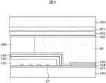
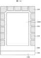
図2は、図1のA−A断面に相当するシール部の詳細断面図である。シール部の断面形状は表示領域の断面形状とは異なる。表示領域に形成される層のうち、シール部に不要な層は省略されている。図2において、ガラスで形成されたTFT基板100に第1の絶縁膜101が形成されている。第1の絶縁膜101は走査線と映像信号線の間を絶縁する層間絶縁膜である場合もあるし、ゲート絶縁膜の場合もある。 FIG. 2 is a detailed cross-sectional view of a seal portion corresponding to the AA cross section of FIG. The cross-sectional shape of the seal portion is different from the cross-sectional shape of the display area. Of the layers formed in the display area, layers unnecessary for the seal portion are omitted. In FIG. 2, a first
第1の絶縁膜101の上に信号線の引き出し線21が形成されている。この引き出し線21は、図1における図面上方から下方に延在する引き出し線であるか、図1には記載されていない。引き出し線21を覆って、有機パッシベーション膜102が形成されている。有機パッシベーション膜102は平坦化膜としての役割も有するので、2μm程度と厚く形成されている。有機パッシベーション膜102の上に層間絶縁膜103がCVD等によって形成されている。層間絶縁膜103は、表示領域において、第1の電極と第2の電極を絶縁するためのものである。層間絶縁膜103を覆って第1ITO104が形成されている。 A
図2において、TFT基板100の端部側においては、第1の絶縁膜101の上に第1ITO104が形成されている。そして、第1ITO104を覆って配向膜105が形成されている。このように、配向膜105の下層にITO104が形成されていることが本発明の特徴である。層間絶縁膜103はSiNx(窒化シリコン)で形成されており、第1の絶縁膜101もSiNxで形成されている場合が多いが、SiO2の場合もある。SiNxもSiO2も同様な性質を持っているので、以下、SiNxで代表して説明する。SiNxと配向膜との接着力は弱い。一方、配向膜とITOとの接着力は強いので、本発明ではシール部の信頼性を向上することが出来る。In FIG. 2, the
第1ITO104は電気的にはフロートの状態である。外側の第1ITO104は、TFT基板100の端部まで形成されているので、端部から静電気が侵入しやすい。しかし、外側の第1ITO104と内側の第1ITO104とは、有機パッシベーション膜102の端部において分離されており、外部から静電気が侵入しても、静電気が内部の第1ITO104や配線に侵入しないようにしている。 The
図2において、TFT基板100に対向して対向基板200が配置している。対向基板200には、カラーフィルタ層201が形成され、その上(TFT基板側)にオーバーコート膜202が形成され、オーバーコート膜202の上に配向膜105が形成されている。なお、カラーフィルタ層201は、品種によってはTFT基板100側に形成されることもある。TFT基板100と対向基板200とはシール材30によって接着し、シール材30より内側に液晶300が封入されている。 In FIG. 2, a
シール材30は、TFT基板100側、対向基板200側ともに、配向膜105と接着している。配向膜105の接着力は、特に、TFT基板100側におけるSiNx膜104との間で問題となる。本発明では、TFT基板100側のシール部においては、配向膜105はほとんどITO104と接着しているので、シール部の信頼性は高い。 The sealing
図3はTFT基板100側において、第1ITO104が形成されている範囲とシール材30が形成されている範囲を示す模式平面図である。図3において、配向膜はTFT基板100全面に形成されている。図3において、外側の第1ITO104は、TFT基板の辺に沿って島状に形成され、さらに、ギャップを挟んで内側の第1ITO104が形成されている。図では、外側の第1ITO104も内側の第1ITO104も電気的にはフロートとなっているが、内側の第1ITO104にコモン電圧(Vcom)や電源等の他の電圧を供給するものであってもよい。そして外側の第1ITO104と内側の第1ITO104は、電気的には互いに絶縁されている。 FIG. 3 is a schematic plan view showing a range where the
シール材30は、TFT基板100あるいは、対向基板200の端部から点線までのハッチングで示す領域に形成されている。図3に示すように、シール材30は、TFT基板100側においては、大部分の領域において、第1ITO104とオーバーラップしている。ただし、端子領域150側の辺においては、配向膜の下には第1ITOは形成されていない。端子領域150側では、配線が高い密度で形成されているので、第1ITO150を通した静電気の影響が大きいからである。一方、端子領域150側の辺においては、他の辺に比べてスペース的に余裕がある。そのため、端子領域150側の辺のシール材30の幅を他の辺のシールの幅よりも太くし、接着面積を他の辺よりも大きくすることが出来るため、その分接着強度を大きくできる。 The sealing
図4は、図3の長辺側または短辺側のシール部における第1ITO104、シール材30等の寸法の関係を示す拡大平面図である。図4において、シール材30は、TFT基板100端部からw3の範囲で形成されており、島状の外側第1ITO104は、TFT基板100端部から幅w1で形成されており、内側第1ITO104はTFT基板100端部からw2の距離より内側方向に幅w4で、TFT基板100の辺方向にストライプ状に延在している。内側の第1ITO104の端部は、図4では、シール材30の内側端部よりもさらに表示領域1000側方向に形成されている。ただし、第1ITO104の目的は、シール部における接着強度の向上であるから、内側第1ITO104の内側端部は、シール材30の内側端部と同じであってもよいし、接着に大きな影響を与えなければ、シール材30の内側よりも、外側、すなわち、シール材30の中心側に位置していてもよい。 FIG. 4 is an enlarged plan view showing a dimensional relationship of the
外側第1ITO104と内側第1ITO104との間にはg2なるギャップが存在し、外部から侵入してきた静電気が内側の第1ITO104に流れ込まないようにしている。島状に形成された外側ITO104のTFT基板100の辺に沿う長さはh1であり、島状第1ITO104と島状第1ITO104の間隔はg1である。シール材30と内側あるいは外側第1ITO104が存在しない部分においては、シール材は層間絶縁膜103すなわち、SiNxと接している。配向膜の接着強度を向上させるためには、g1は小さいほうがよい。 There is a gap g2 between the outer
具体的な数値の例は次のとおりである。すなわち、島状の外側第1ITO104の大きさを決めるw1は100μm、h1は150μmである。また、島状第1ITO104と島状第1ITO104の間隔は5μm以上、好ましくは10μm以上で、50μm以下であることが望ましい。また、島状の外側第1ITO104とストライプ状の内側第1ITO104との間隔g2も5μm以上、好ましくは10μm以上で、50μm以下であることが望ましい。g1もg2も、下限は、静電気が他の領域に入り込まないようにするためであり、上限は、配向膜と第1ITOが接触する面積をできるだけ大きくするためである。 Examples of specific numerical values are as follows. That is, w1 which determines the size of the island-shaped outer
図4において、シール材30の幅w3は400μm、内側第1ITO104は、w2=w1+g2の位置から内側に幅w4で形成されている。w2は例えば150μmである。また、島状の第1ITO104は、TFT基板100の端部に形成されているので、静電気が入りやすいため、幅w1は制限した方がよい。例えば、外側の島状第1ITO104の幅(w1)/シール材の幅(w3)は35%以下に抑えることが望ましい。また、接着強度の観点からは、シール材30の幅w3に対する、外側第1ITO104と内側第1ITO104の間隔g2の割合は、15%以下とすることが望ましい。 In FIG. 4, the width w3 of the sealing
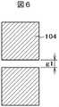
外側第1ITO104の形状は図3あるいは図4の形状に限る必要はない。図5および図6は、外側第1ITO104の形状の他の例である。図5は外側第1ITO104を小さなタイル状に形成した場合であり、図6は外側第1ITO104を大きなタイル状に形成した場合である。図5の形状は、静電気が侵入した場合、静電気の影響を小さな領域に抑え込むことが出来る。しかし、第1ITO104の下側の層間絶縁膜103が露出する面積の割合が増えるので接着力は低下する。一方、図6の形状は、侵入した静電気の影響が図5の領域よりも大きいが、層間絶縁膜103の露出面積の割合を小さくすることが出来るので、接着力の点では優れている。また、内側第1ITO104についても、図では1本設けているが、2本以上設けることも可能である。また、設けないことも可能である。基板の一部における内側第1ITO104に対して、他の部分の内側第1ITO104を太く設けたり、本数を多く設けたりすることも可能である。内側第1ITO104を複数本設ける場合、基板の外側に近い側の内側第1ITO104をフローティングとし、他の内側第1ITO104に対してコモン電圧等の所定の電位を印加するものであってもよい。 The shape of the outer
図5においては、第1ITO104は横方向に2列のみ形成されているが、3列以上形成してもよい。また、マトリクス状ではなく、千鳥状(ある列に対して隣接する列をずらす形状)としてもよい。また、基板の端部側の島と内側の島との大きさを異ならせることも可能である。なお、島状の第1ITO104の間の絶縁を維持しつつ、シール部における第1ITO104の面積の割合を大きくするには、第1ITO104の形状は、タイル状にすることが合理的である。 In FIG. 5, the
外側第1ITO104の形状は、TFT基板100の辺全体にわたって同じである必要はない。液晶表示パネルのコーナ部においては引きはがし応力が大きいので、コーナ部においては第1ITO104を図6のような形状とし、辺部(コーナー部とコーナ部との間)においては、静電気対策を重視して、図5のような形状にすることもできる。 The shape of the outer
以上の説明では、ITOとして、第1ITO104のみを用いるということで説明した。IPS方式液晶表示装置では、先に説明したように、TFT基板100側に第1ITOを用いた第1の電極と第2ITOを用いた第2電極が存在するので、シール部における配向膜の接着強度の向上のために、第1ITOと第2ITOの両方を用いることもできる。図7は、図3の外側ITOとして、第1ITO104と第2ITO106を用いた場合の平面図であり、図8は図7のB−B断面図である。図7および図8においては、第2ITO106を大きなタイル状に形成し、第1ITO104を小さなタイル状に形成している。このような構成とすることによって、ITO膜の表面が凹凸化されるので、この点から、配向膜とITOの接着力をさらに強化することが出来る。この場合、島状の第1ITOとが第2ITO106を介して電気的に接続しているのが、島状の第1ITO間の第2ITO106にスリットを設けることも可能である。これにより、外部からの静電気の侵入を防止することが可能となる。また、第1ITOと第2ITOとの間に島状に絶縁膜を残存させることも可能である。 In the above description, only the
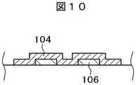
図9及び図10は第1ITO104と第2ITO106を用いた場合の他の例である。図9は、第2ITO106を小さなタイル状に形成し、第1ITO104を大きなタイル状に形成した場合の平面図であり、図10は図9のC−C断面図である。図9および図10の効果は、図7及び図8の構成で説明したのと同様である。この場合も、第1ITO104にスリットを設けたり、島状の第2ITOを覆うように島状の絶縁膜を残存させる構成であってもよい。 FIG. 9 and FIG. 10 are other examples when the
以上で説明した第1ITO104では、外側第1ITO104を島状に形成し、内側第1ITOをTFT基板の辺に平行なストライプ状に形成している。しかし、内側第1ITO104はストライプ状に限る必要はなく、図11に示すように島状に形成してもよい。図11では、内側第1ITO104の大きさは、外側第1ITO104の大きさよりも大きい島状であるが、これに限らず、内側第1ITO104を外側第1ITO104と同様な形状としても良いし、図11とは逆に内側第1ITO104が外側第1ITO104よりも小さい島形状としてもよい。 In the
図12乃至図17は、配向膜の接着力を向上させるための第1ITOの種々の例を示すものである。図12乃至図17は、図1におけるTFT基板の端部から表示領域の端部までの幅dにおいて、1個の島状の第1ITO104が形成されているが、これは例であって、実施例1で説明したように、図1の幅d内において、島状第1ITOを複数形成してもよい。 12 to 17 show various examples of the first ITO for improving the adhesion of the alignment film. 12 to 17, one island-shaped
図12は、TFT基板100において、辺部では第1ITO100の外側端部をTFT基板100の端部から所定の距離d1だけ内側に離し、TFT基板100のコーナ部では、第1ITO104をTFT基板100の端部にまで形成した例である。液晶表示パネルのコーナ部では、TFT基板と対向基板を引きはがす応力が辺部に比較して大きいので、コーナ部は、第1ITO104をTFT基板100の端部にまで形成し、辺部では、TFT基板100の端部からd1だけ離すことによって、静電気の侵入を防止しやすくしている。図12においても、端子領域150側の辺には、第1ITO104は形成していない。理由は実施例1で説明したのと同じである。尚、図12中、下側の辺を除く3辺において、第1ITO104が基板端部から離間しているが、一部の辺においては、辺部の第1ITO104が基板端部まで延在するものであってもよい。 12 shows that the outer edge of the
図13は図12とは逆にTFT基板100のコーナ部においては、島状の第1ITO104の端部をTFT基板100の端部から所定の距離d2だけ内側に形成し、TFT基板100の辺部においては島状の第1ITO104をTFT基板100の端部まで形成した例である。コーナ部において、目合せマークを形成する等のレイアウト上の要請からTFT基板100のコーナ端部にまで、第1ITO104を形成できないような事情がある場合にこのような構成をとることが出来る。一方、図13において、辺部では、TFT基板100の端部にまで、第1ITO104が形成されているので、辺部において、配向膜の必要な接着力を確保している。図13においても、端子領域150側には第1ITO104は形成されていない。 In FIG. 13, contrary to FIG. 12, in the corner portion of the
図14は、第1ITO104の端部がコーナ部においても、辺部においても、TFT基板100の端部にまで形成されているが、コーナ部における第1ITO104の内側形状がコーナカットしたような形状になっている。配線の引き出し線がコーナ部において、90度ではなく、所定の角度で折れ曲がって配線されているような場合、配線に沿って、島状の第1ITO104をコーナカット形状とすることによって、引き出し線と島状第1ITO104がオーバーラップすることを防止することが出来る。 In FIG. 14, the end of the
図15は、端子領域150側にも島状の第1ITO104を形成した例である。これまでの実施例では、端子領域150側には第1ITO140を設けない構成を示してきたが、端子領域150側の辺においてもシール部の接着力が問題となる場合がある。図15において、端子領域150側以外の辺においては、第1ITO104はTFT基板100の端部にまで形成され、端子領域150側では、対向基板200の端部に対応する部分にまで第1ITO104が形成されている。 FIG. 15 shows an example in which the island-like
端子領域150側の辺では、引き出し配線が密集しているので、静電気対策が重要となる。この対策としては、端子領域150側の辺において、他の辺よりも第1ITO104のサイズを小さくする、あるは、第1ITO104の形状を他の辺とは異なる形状にする等によって、対処することが出来る。さらには、膜厚の厚い、有機パッシベーション膜を端子領域側のシール部の外側端部にまで延在させることによって、静電気に対する耐性を向上させることが出来る。 On the side on the
図16は、対向基板200とTFT基板100が接着しているシール部の4コーナ部のみにおいて、配向膜の下に第1ITO104を配置した例である。この場合も配向膜の下層に形成された第1ITO104は、TFT基板100の端部にまで形成されている。シール部における引きはがし応力は、4コーナ部において大きいからである。一方、液晶表示パネルの辺部においては、端部に第1ITO104が存在していないので、広い領域において静電気の問題を避けることが出来る。 FIG. 16 shows an example in which the
図17は、対向基板200とTFT基板100が接着しているシール部において、端子領域150から遠い、2コーナにおいてのみ、配向膜の下に第1ITO104を配置した例である。この場合も配向膜の下層に形成される第1ITO104は、TFT基板100の端部にまで形成されている。シール材における引きはがし応力は、端子領域150から最も遠い2コーナにおいて最も大きいからである。一方、液晶表示パネルの辺部を含む他の部分においては、端部に第1ITO104が存在していないので、広い領域において静電気の問題を避けることが出来る。 FIG. 17 shows an example in which the
IPS方式は、はプレティルト角が必要でないため、配向膜に対する配向処理として、いわゆる光配向方式が適している。光配向は、偏光紫外線を照射することによって、特定方向の高分子の鎖を破壊し、配向膜に一軸異方性を与え、配向特性を発揮させるものである。光配向処理された配向膜は、光配向以外の配向処理を受けた配向膜に比べて、シール材あるいは配向膜の下層の膜との接着性が低いという性質がある。したがって、以上で述べた本発明は、光配向処理されたIPS方式の液晶表示装置に特に適している。しかし、光配向処理されたIPS方式の液晶表示装置であっても、本願発明を適用することで、狭額縁化、接着力強化を実現することが可能となる。 Since the IPS method does not require a pretilt angle, a so-called photo-alignment method is suitable as an alignment treatment for the alignment film. In photo-alignment, irradiation with polarized ultraviolet rays breaks polymer chains in a specific direction, imparts uniaxial anisotropy to the alignment film, and exhibits alignment characteristics. An alignment film that has been subjected to photo-alignment treatment has a property that adhesion to a sealing material or a lower layer of the alignment film is lower than an alignment film that has undergone alignment treatment other than photo-alignment. Therefore, the present invention described above is particularly suitable for an IPS liquid crystal display device subjected to photo-alignment treatment. However, even with an IPS liquid crystal display device that has been subjected to photo-alignment processing, it is possible to realize a narrow frame and enhanced adhesion by applying the present invention.
以上の説明では、配向膜の接着強度を向上させる材料として、ITOを使用するとして説明した。これは、第1電極あるいは第2電極を構成する酸化物導電膜がITOであるという前提での構成である。しかし、酸化物導電膜は、ITOに限らず、IZO(Indium Tin Oxide)等が使用されることもある。画素における第1電極あるいは第2電極としてIZO等が使用される場合は、TFT基板あるいは対向基板の端部において配向膜の下層に形成される酸化物導電膜にIZO等を使用することが出来る。 In the above description, it has been described that ITO is used as a material for improving the adhesive strength of the alignment film. This is a configuration on the assumption that the oxide conductive film constituting the first electrode or the second electrode is ITO. However, the oxide conductive film is not limited to ITO, and IZO (Indium Tin Oxide) or the like may be used. When IZO or the like is used as the first electrode or the second electrode in the pixel, IZO or the like can be used for the oxide conductive film formed in the lower layer of the alignment film at the end of the TFT substrate or the counter substrate.
以上は、本発明をIPS方式について説明したが、本発明は、IPSに限らず、VA(Vertical Alignmnet)方式あるいはTN(Twisted Nematic)方式の液晶表示装置についても適用することが出来る。VA方式では、負の誘電率異方性を有する液晶を使用する。VAは、無電界の状態では、液晶分子はTFT基板あるいは対向基板の平面と直角方向に配向し、電界が印加されると液晶分子が傾いて、液晶層を通過する光の透過率を制御するものである。TN方式は、無電界の状態では、液晶分子をTFT基板側から対向基板側に向かうにしたがって、液晶分子の配向方向を90度捩じるよう初期配向させておき、電界を印加することによって、初期配向方向から変化させ、電界の強度に応じて初期配向方向から変化する量を制御して液晶層を通過する光の透過率を制御するものである。 Although the present invention has been described with respect to the IPS system, the present invention is not limited to the IPS, but can be applied to a VA (Vertical Alignnet) system or a TN (Twisted Nematic) system liquid crystal display device. In the VA mode, a liquid crystal having negative dielectric anisotropy is used. In VA, liquid crystal molecules are aligned in a direction perpendicular to the plane of the TFT substrate or the counter substrate in the absence of an electric field, and the liquid crystal molecules are tilted when an electric field is applied to control the transmittance of light passing through the liquid crystal layer. Is. In the TN mode, in the state of no electric field, the liquid crystal molecules are initially aligned so as to twist the alignment direction of the liquid crystal molecules by 90 degrees from the TFT substrate side toward the counter substrate side, and an electric field is applied, The transmittance of light passing through the liquid crystal layer is controlled by changing from the initial alignment direction and controlling the amount of change from the initial alignment direction according to the strength of the electric field.
VA、TN等では、TFT基板側に透明導電膜による画素電極が形成され、対向基板側には透明導電膜によるコモン電極が形成されている。したがって、TFT基板側および対向基板側の両方において、基板の端部にまで配向膜の下にITOを形成する構成とすることが出来る。 In VA, TN, etc., a pixel electrode made of a transparent conductive film is formed on the TFT substrate side, and a common electrode made of a transparent conductive film is formed on the counter substrate side. Therefore, on both the TFT substrate side and the counter substrate side, the ITO can be formed below the alignment film up to the end of the substrate.
VA方式あるいは、TN方式において、対向基板側の端部にITOを形成する場合も、ITOは配向膜の下層に形成される。すなわち、図2について言えば、配向膜とオーバーコート膜の間に形成されることになる。そのため、本願発明を、TFT基板に設けられるITOのみならず、対向基板に設けられるITOに対して適用することが可能である。もちろん、TFT基板のITOと対向基板のITOとの双方に適用することも可能である。 In the VA method or the TN method, when ITO is formed at the end portion on the counter substrate side, the ITO is formed below the alignment film. That is, with respect to FIG. 2, it is formed between the alignment film and the overcoat film. Therefore, the present invention can be applied not only to the ITO provided on the TFT substrate but also to the ITO provided on the counter substrate. Of course, the present invention can be applied to both the ITO of the TFT substrate and the ITO of the counter substrate.
10…走査線、 20…映像信号線、 21…信号線の引出し線、 25…画素、 30…シール材、 100…TFT基板、 101…第1の絶縁膜、 102…有機パッシベーション膜、 103…層間絶縁膜、 104…第1ITO、 105…配向膜、 106…第2ITO透明導電膜、 150…端子領域、 160…ICドライバ、 200…対向基板、 201…カラーフィルタ層、 202…オーバーコート膜、 300…液晶、 1000…表示領域 DESCRIPTION OF
Claims (16)
Translated fromJapanese前記TFT基板は表示領域と端子領域とを有し、前記表示領域は、前記シール材に囲まれた領域に形成され、
前記TFT基板において、前記シール材と前記TFT基板との間には配向膜が存在し、前記配向膜と前記TFT基板との間には酸化物導電膜が存在し、前記酸化物導電膜は、前記TFT基板の端部にまで形成され、
前記酸化物導電膜はフロートであることを特徴とする液晶表示装置。A liquid crystal display device comprising: a TFT substrate having a pixel electrode and an alignment film; a counter substrate facing the TFT substrate; a seal and a liquid crystal provided between the TFT substrate and the counter substrate;
The TFT substrate has a display area and a terminal area, and the display area is formed in an area surrounded by the sealing material,
In the TFT substrate, an alignment film exists between the sealing material and the TFT substrate, an oxide conductive film exists between the alignment film and the TFT substrate, Formed to the end of the TFT substrate,
The liquid crystal display device, wherein the oxide conductive film is a float.
前記対向基板側酸化物導電膜はフロートであることを特徴とする請求項1乃至11の何れかに記載の液晶表示装置。In the counter substrate, a counter substrate side alignment film is present below the sealing material, a counter substrate side oxide conductive film is present below the counter substrate side alignment film, and the counter substrate side oxide conductive film is present. Is formed up to the end of the counter substrate,
12. The liquid crystal display device according to claim 1, wherein the counter-substrate-side oxide conductive film is a float.
Priority Applications (3)
| Application Number | Priority Date | Filing Date | Title |
|---|---|---|---|
| JP2015121703AJP2017009637A (en) | 2015-06-17 | 2015-06-17 | Liquid crystal display |
| US15/160,411US10209575B2 (en) | 2015-06-17 | 2016-05-20 | Liquid crystal display device |
| US16/242,693US20190162995A1 (en) | 2015-06-17 | 2019-01-08 | Liquid crystal display device |
Applications Claiming Priority (1)
| Application Number | Priority Date | Filing Date | Title |
|---|---|---|---|
| JP2015121703AJP2017009637A (en) | 2015-06-17 | 2015-06-17 | Liquid crystal display |
Publications (1)
| Publication Number | Publication Date |
|---|---|
| JP2017009637Atrue JP2017009637A (en) | 2017-01-12 |
Family
ID=57587832
Family Applications (1)
| Application Number | Title | Priority Date | Filing Date |
|---|---|---|---|
| JP2015121703APendingJP2017009637A (en) | 2015-06-17 | 2015-06-17 | Liquid crystal display |
Country Status (2)
| Country | Link |
|---|---|
| US (2) | US10209575B2 (en) |
| JP (1) | JP2017009637A (en) |
Families Citing this family (1)
| Publication number | Priority date | Publication date | Assignee | Title |
|---|---|---|---|---|
| JP7274935B2 (en)* | 2019-05-24 | 2023-05-17 | 株式会社ジャパンディスプレイ | Display device |
Family Cites Families (12)
| Publication number | Priority date | Publication date | Assignee | Title |
|---|---|---|---|---|
| JPH10206871A (en) | 1997-01-27 | 1998-08-07 | Sanyo Electric Co Ltd | Liquid crystal display device and its production method |
| US7898632B2 (en)* | 2005-12-28 | 2011-03-01 | Seiko Epson Corporation | Electro-optical device, manufacturing method thereof, and electronic apparatus |
| JP2012083513A (en)* | 2010-10-12 | 2012-04-26 | Seiko Epson Corp | Liquid crystal device, and electronic device |
| JP5853419B2 (en)* | 2010-10-25 | 2016-02-09 | セイコーエプソン株式会社 | Electro-optical device, electronic apparatus, and substrate for electro-optical device |
| JP2012189856A (en) | 2011-03-11 | 2012-10-04 | Seiko Instruments Inc | Liquid crystal display device |
| JP2012198395A (en)* | 2011-03-22 | 2012-10-18 | Seiko Epson Corp | Liquid crystal device and projection type display device |
| JP2012208301A (en)* | 2011-03-29 | 2012-10-25 | Seiko Epson Corp | Liquid crystal device and projection type display device |
| JP5699741B2 (en)* | 2011-03-29 | 2015-04-15 | セイコーエプソン株式会社 | Liquid crystal device and projection display device |
| JP2012255840A (en)* | 2011-06-07 | 2012-12-27 | Japan Display West Co Ltd | Display device and electronic apparatus |
| JP6014978B2 (en)* | 2011-09-22 | 2016-10-26 | ソニー株式会社 | Liquid crystal display element and liquid crystal display device |
| JP6205113B2 (en)* | 2012-08-24 | 2017-09-27 | 株式会社ジャパンディスプレイ | Liquid crystal display |
| CN104603685B (en)* | 2012-09-04 | 2017-04-19 | 夏普株式会社 | Liquid crystal display device |
- 2015
- 2015-06-17JPJP2015121703Apatent/JP2017009637A/enactivePending
- 2016
- 2016-05-20USUS15/160,411patent/US10209575B2/enactiveActive
- 2019
- 2019-01-08USUS16/242,693patent/US20190162995A1/ennot_activeAbandoned
Also Published As
| Publication number | Publication date |
|---|---|
| US20160370618A1 (en) | 2016-12-22 |
| US10209575B2 (en) | 2019-02-19 |
| US20190162995A1 (en) | 2019-05-30 |
Similar Documents
| Publication | Publication Date | Title |
|---|---|---|
| US11852923B2 (en) | Liquid crystal display device | |
| CN103869554B (en) | Display panels | |
| US9847426B2 (en) | Display device | |
| US8576365B2 (en) | Display panel | |
| JP2006259725A (en) | Horizontal electric field type liquid crystal display element and method for manufacturing the same | |
| WO2013154022A1 (en) | Liquid crystal display device | |
| US7843543B2 (en) | Liquid crystal display device | |
| US10203568B2 (en) | Liquid crystal display device | |
| JP2010134294A5 (en) | ||
| CN104204928A (en) | Liquid crystal display panel | |
| US8610856B2 (en) | Liquid crystal display device | |
| CN101435967B (en) | Active matrix liquid crystal display device | |
| JP2017009637A (en) | Liquid crystal display | |
| JP5137241B2 (en) | Liquid crystal display | |
| KR101201324B1 (en) | In-plane switching mode liquid crystal display device | |
| JP4986307B2 (en) | Liquid crystal display | |
| JP6739564B2 (en) | Liquid crystal display | |
| KR102011951B1 (en) | Liquid Crystal Display Having High Aperture Ratio And High Transmittance Ratio | |
| JP5197873B2 (en) | Liquid crystal display | |
| KR20140085778A (en) | Large Area In-Plane Switching Liquid Crystal Display | |
| JP2020139968A (en) | Display device |