JP2017005948A - Power supply circuit and game machine - Google Patents
Power supply circuit and game machineDownload PDFInfo
- Publication number
- JP2017005948A JP2017005948AJP2015120643AJP2015120643AJP2017005948AJP 2017005948 AJP2017005948 AJP 2017005948AJP 2015120643 AJP2015120643 AJP 2015120643AJP 2015120643 AJP2015120643 AJP 2015120643AJP 2017005948 AJP2017005948 AJP 2017005948A
- Authority
- JP
- Japan
- Prior art keywords
- circuit
- load current
- signal
- input
- threshold
- Prior art date
- Legal status (The legal status is an assumption and is not a legal conclusion. Google has not performed a legal analysis and makes no representation as to the accuracy of the status listed.)
- Granted
Links
- 238000001514detection methodMethods0.000claimsabstractdescription91
- 230000004044responseEffects0.000claimsdescription10
- 230000004913activationEffects0.000abstractdescription8
- 230000000694effectsEffects0.000description16
- 238000010586diagramMethods0.000description15
- 238000009499grossingMethods0.000description7
- 239000003990capacitorSubstances0.000description6
- 230000004048modificationEffects0.000description6
- 238000012986modificationMethods0.000description6
- 230000002159abnormal effectEffects0.000description5
- 238000004519manufacturing processMethods0.000description5
- 230000008859changeEffects0.000description4
- 239000000470constituentSubstances0.000description4
- 230000007704transitionEffects0.000description4
- 230000003321amplificationEffects0.000description2
- 230000007423decreaseEffects0.000description2
- 230000007257malfunctionEffects0.000description2
- 238000003199nucleic acid amplification methodMethods0.000description2
- 230000035945sensitivityEffects0.000description2
- 239000000428dustSubstances0.000description1
- 238000009429electrical wiringMethods0.000description1
- 238000005259measurementMethods0.000description1
- 238000009987spinningMethods0.000description1
- 230000001360synchronised effectEffects0.000description1
Images


Landscapes
- Rectifiers (AREA)
- Pinball Game Machines (AREA)
- Emergency Protection Circuit Devices (AREA)
Abstract
Description
Translated fromJapanese本発明は、電源回路及びそのような電源回路を利用する遊技機に関する。 The present invention relates to a power supply circuit and a gaming machine using such a power supply circuit.
遊技機において、負荷回路に供給する負荷電流を監視して、負荷電流が所定の検出値以上であるときに過電流が流れたと判定して、負荷回路への電流の供給を停止する電源回路が知られている(例えば、特許文献1を参照)。 In the gaming machine, a power supply circuit that monitors the load current supplied to the load circuit, determines that an overcurrent has flowed when the load current is equal to or greater than a predetermined detection value, and stops supplying the current to the load circuit. It is known (see, for example, Patent Document 1).
特許文献1には、第1過電流検出値と、第1過電流検出値より大きい第2過電流検出値との2段階の過電流検出値を設定可能な電源回路が記載される。特許文献1に記載される電源回路は、電源投入されてからの経過時間が所定時間を超え且つ負荷に供給される出力電圧が所定電圧以上のときに、第1過電流検出値により過電流検出を行う。また、特許文献1に記載される電源回路は、電源投入されてからの経過時間が所定時間を超える前の起動時に、電源起動時の突入電流(ラッシュ電流とも称される)の最大値以上の比較的大きな検出値である第2過電流検出値により過電流検出を行う。特許文献1に記載される電源回路では、第2過電流検出値を電源起動時の突入電流の最大値以上にすることにより、突入電流によって過電流検出機能が誤動作することを防止することができる。
しかしながら、特許文献1に記載される電源回路では、塵芥等が遊技機の内部に侵入して電気配線に付着して生じる短絡(以下、レアショートとも称する)による過電流等の比較的小さな過電流を検出することは容易ではない。特許文献1に記載される電源回路では、起動時の過電流検出値を電源起動時の突入電流の最大値以上と比較的大きくするので、レアショートに起因する過電流を起動時に検出することはできない。また、レアショートに起因する過電流を検出可能とするために、通常動作時の過電流検出値を小さくすると、遊技機の定常動作による電流の変動により過電流検出機能が誤動作するおそれがある。このため、特許文献1に記載される電源回路では、遊技機の定常動作時においても、レアショートに起因する過電流を検出することはできない。 However, in the power supply circuit described in
そこで、本発明は、レアショート等に起因する比較的小さい過電流を検出可能な電源回路を提供することを目的とする。 Accordingly, an object of the present invention is to provide a power supply circuit capable of detecting a relatively small overcurrent caused by a rare short or the like.
上記の目的を達成するために、本発明の一つの形態に係る電源回路は、遊技機に設けられた負荷回路に電力を供給する電源回路であって、入力された交流を直流に変換する整流回路と、オン状態のときに整流回路と負荷回路との間を接続し、オフ状態のときに整流回路と負荷回路との間の接続を遮断するスイッチング回路と、スイッチング回路がオン状態のときに整流回路から負荷回路に流れる負荷電流を検出する負荷電流検出回路と、負荷電流検出回路に接続され、負荷電流が第1閾値以上であるときに、第1過電流信号を出力する第1比較回路と、負荷電流検出回路に接続され、交流が整流回路に入力されてから所定の起動時間が経過するまでの間に負荷電流が第1閾値よりも小さい第2閾値以上であるときに、第2過電流信号を出力する第2比較回路と、負荷電流検出回路に接続され、負荷電流が所定の連続時間に亘って第1閾値よりも小さく且つ第2閾値よりも大きい第3閾値より大きいときに、第3過電流信号を出力する第3比較回路と、第1比較回路、第2比較回路及び第3比較回路に接続され、第1過電流信号又は第3過電流信号が入力されたこと、若しくは第2過電流信号が所定の継続時間に亘って連続して入力されたことに応じて、スイッチング回路をオフ状態にする過電流制御回路と、を有する。 In order to achieve the above object, a power supply circuit according to one aspect of the present invention is a power supply circuit that supplies power to a load circuit provided in a gaming machine, and rectifies the input alternating current into direct current. A switching circuit that connects between the rectifier circuit and the load circuit when the circuit is on, and disconnects the connection between the rectifier circuit and the load circuit when the circuit is off, and when the switching circuit is on A load current detection circuit that detects a load current flowing from the rectifier circuit to the load circuit, and a first comparison circuit that is connected to the load current detection circuit and outputs a first overcurrent signal when the load current is equal to or greater than a first threshold value. And when the load current is greater than or equal to a second threshold value smaller than the first threshold value after the predetermined start-up time elapses after AC is input to the rectifier circuit. Output overcurrent signal A third overcurrent signal is connected to the second comparison circuit and the load current detection circuit and when the load current is larger than a third threshold value that is smaller than the first threshold value and larger than the second threshold value over a predetermined continuous time. Is connected to the first comparison circuit, the first comparison circuit, the second comparison circuit, and the third comparison circuit, and the first overcurrent signal or the third overcurrent signal is input, or the second overcurrent signal. And an overcurrent control circuit that turns off the switching circuit in response to continuous input for a predetermined duration.
また、この電源回路において、過電流制御回路は、第1比較回路及び第2比較回路に接続され、第1過電流信号又は第2過電流信号の入力が継続する時間を計時する継続時間計時回路と、継続時間計時回路に接続され、継続時間計時回路が計時した時間が継続時間に達したときに、オフ状態にすることを示すオフ指示信号をスイッチング回路に出力するスイッチ制御回路と、を有することが好ましい。 Further, in this power supply circuit, the overcurrent control circuit is connected to the first comparison circuit and the second comparison circuit, and the duration measuring circuit counts the time during which the input of the first overcurrent signal or the second overcurrent signal continues. And a switch control circuit that is connected to the duration time counting circuit and outputs an off instruction signal to the switching circuit indicating that the duration time is reached when the time counted by the duration time counting circuit reaches the duration time. It is preferable.
また、この電源回路において、第1比較回路は、負荷電流の変動を予測する負荷予測信号が入力されたことに応じて、第1閾値に対応する第1閾値電圧を変更する閾値変更回路と、負荷電流に対応する検出電圧と第1閾値電圧とを比較し、負荷電流が第1閾値電圧以上のときに第1過電流信号を出力する第1コンパレータと、を有することが好ましい。 Further, in the power supply circuit, the first comparison circuit changes a first threshold voltage corresponding to the first threshold in response to input of a load prediction signal for predicting a change in load current; It is preferable to have a first comparator that compares the detection voltage corresponding to the load current with the first threshold voltage and outputs a first overcurrent signal when the load current is equal to or higher than the first threshold voltage.
また、この電源回路において、第2比較回路は、負荷電流に対応する検出電圧と第2閾値に対応する第2閾値電圧とを比較し、検出電圧が第2閾値電圧以上のときに第2過電流信号を出力する第2コンパレータと、整流回路に交流が入力されてからの時間を計時し、計時した時間が起動時間を経過したときに、起動時間経過信号を出力する起動時間計時回路と、第2コンパレータ及び起動時間計時回路に接続され、起動時間経過信号が入力される前に、第2過電流信号が入力されたときに、第2過電流信号を出力し、起動時間経過信号が入力された後に、第2過電流信号が入力されたときに、第2過電流信号を出力しない無効化回路と、を有することが好ましい。 Further, in this power supply circuit, the second comparison circuit compares the detection voltage corresponding to the load current with the second threshold voltage corresponding to the second threshold, and when the detection voltage is equal to or higher than the second threshold voltage, the second comparison circuit. A second comparator for outputting a current signal, a time for measuring the time since AC is input to the rectifier circuit, and a start-up time counting circuit for outputting a start-up time lapse signal when the measured time has passed the start-up time; The second overcurrent signal is output when the second overcurrent signal is input before the startup time elapsed signal is input, and the second overcurrent signal is output and the startup time elapsed signal is input. And a disabling circuit that does not output the second overcurrent signal when the second overcurrent signal is input.
また、この電源回路において、第3比較回路は、負荷電流に対応する検出電圧と第3閾値に対応する第3閾値電圧とを比較し、検出電圧が第3閾値電圧以下のときにリセット信号を出力する第3コンパレータと、所定のパルス周期でパルス信号を出力するパルス生成回路と、第3コンパレータ及びパルス生成回路に接続され、パルス信号が入力されたカウント数を計数し、リセット信号が入力されたときにカウント数をリセットするカウンタと、カウンタに接続され、カウント数が所定のカウント閾値と等しくなったときに、第3過電流信号を出力する高電流状態判定回路と、を有することが好ましい。 In this power supply circuit, the third comparison circuit compares the detection voltage corresponding to the load current with the third threshold voltage corresponding to the third threshold value, and outputs a reset signal when the detection voltage is equal to or lower than the third threshold voltage. A third comparator that outputs, a pulse generation circuit that outputs a pulse signal at a predetermined pulse period, and a third comparator and pulse generation circuit that are connected to each other, count the number of counts to which the pulse signal is input, and receive a reset signal It is preferable to have a counter that resets the count number when it is detected, and a high current state determination circuit that is connected to the counter and outputs a third overcurrent signal when the count number becomes equal to a predetermined count threshold value. .
更に、本発明の他の実施形態によれば、遊技機は、負荷回路と、負荷回路に電力を供給する電源回路であって、入力された交流を直流に変換する整流回路と、オン状態のときに整流回路と負荷回路との間を接続し、オフ状態のときに整流回路と負荷回路との間の接続を遮断するスイッチング回路と、スイッチング回路がオン状態のときに整流回路から負荷回路に流れる負荷電流を検出する負荷電流検出回路と、負荷電流検出回路に接続され、負荷電流が第1閾値以上であるときに、第1過電流信号を出力する第1比較回路と、負荷電流検出回路に接続され、交流が整流回路に入力されてから所定の起動時間が経過するまでの間に負荷電流が第1閾値よりも小さい第2閾値以上であるときに、第2過電流信号を出力する第2比較回路と、負荷電流検出回路に接続され、負荷電流が所定の連続時間に亘って第1閾値よりも小さく且つ第2閾値よりも大きい第3閾値より大きいときに、第3過電流信号を出力する第3比較回路と、第1比較回路、第2比較回路及び第3比較回路に接続され、第1過電流信号又は第3過電流信号が入力されたこと、若しくは第2過電流信号が所定の継続時間に亘って連続して入力されたことに応じて、スイッチング回路をオフ状態にする過電流制御回路と、を有する電源回路と、を有する。 Furthermore, according to another embodiment of the present invention, the gaming machine is a load circuit, a power supply circuit that supplies power to the load circuit, a rectifier circuit that converts input alternating current into direct current, an on-state A switching circuit that sometimes connects between the rectifier circuit and the load circuit, and disconnects the connection between the rectifier circuit and the load circuit when in the off state, and from the rectifier circuit to the load circuit when the switching circuit is in the on state. A load current detection circuit for detecting a flowing load current; a first comparison circuit that is connected to the load current detection circuit and outputs a first overcurrent signal when the load current is equal to or greater than a first threshold; and a load current detection circuit The second overcurrent signal is output when the load current is equal to or greater than a second threshold value that is smaller than the first threshold value after a predetermined start-up time elapses after AC is input to the rectifier circuit. Second comparison circuit and negative charge A third comparison circuit that is connected to the detection circuit and outputs a third overcurrent signal when the load current is smaller than the first threshold and larger than the third threshold greater than the second threshold over a predetermined continuous time; , Connected to the first comparison circuit, the second comparison circuit, and the third comparison circuit, the first overcurrent signal or the third overcurrent signal is input, or the second overcurrent signal is input for a predetermined duration. And an overcurrent control circuit that turns off the switching circuit in response to continuous input.
本発明に係る電源回路は、レアショート等に起因する比較的小さい過電流が検出可能になるという効果を奏する。 The power supply circuit according to the present invention has an effect that it is possible to detect a relatively small overcurrent due to a rare short circuit or the like.
(本発明に係る電源回路の概要)
以下、本発明の実施形態による電源回路を、図を参照しつつ説明する。この電源回路は、負荷回路に流れる負荷電流と、第1閾値及び起動時のみに使用される第1閾値よりも小さい第2閾値とを比較して、負荷電流が第1閾値以上のとき及び第2閾値以上である状態が所定の継続時間に亘って継続したときに、負荷電流を遮断する。加えて、この電源回路は、負荷回路に流れる負荷電流と、第1閾値よりも小さく且つ第2閾値よりも大きい第3閾値とを比較して、負荷電流が第3閾値より大きい状態が所定の連続時間に亘って継続したときに、負荷電流を遮断する。この電源回路は、比較的小さな第2閾値を起動時の過電流検出に使用するものの、負荷電流が第2閾値以上である状態が所定の継続時間に亘って継続したときに負荷電流を遮断するため、瞬時に流れる起動時の突入電流により誤動作するおそれがない。このため、この電源回路では、負荷電流の大きさ及び変動が小さい起動時に第2閾値を使用して負荷電流が過電流を含むか否かを判定できる。更に、定常動作時に負荷電流が第3閾値より大きい状態が所定の連続時間に亘って継続したときに負荷電流が過電流を含むと判断できる。このように、この電源回路では、起動時及び定常動作時の何れでもレアショート等に起因する比較的小さな過電流を検出することができる。(Outline of power supply circuit according to the present invention)
Hereinafter, a power supply circuit according to an embodiment of the present invention will be described with reference to the drawings. The power supply circuit compares a load current flowing through the load circuit with a first threshold and a second threshold that is smaller than the first threshold used only at the time of start-up. When the state of two thresholds or more continues for a predetermined duration, the load current is cut off. In addition, the power supply circuit compares a load current flowing through the load circuit with a third threshold value that is smaller than the first threshold value and larger than the second threshold value, and the state where the load current is larger than the third threshold value is predetermined. When continuing for a continuous time, the load current is cut off. Although this power supply circuit uses a relatively small second threshold value for overcurrent detection at startup, the power supply circuit cuts off the load current when a state where the load current is equal to or greater than the second threshold value continues for a predetermined duration. Therefore, there is no possibility of malfunction due to an inrush current at the time of startup that flows instantaneously. For this reason, in this power supply circuit, it is possible to determine whether or not the load current includes an overcurrent by using the second threshold value at the start-up time when the magnitude and fluctuation of the load current are small. Furthermore, it can be determined that the load current includes an overcurrent when a state in which the load current is larger than the third threshold value continues for a predetermined continuous time during steady operation. As described above, this power supply circuit can detect a relatively small overcurrent caused by a short-circuit or the like at any time of startup and steady operation.
(第1実施形態に係る電源回路の構成)
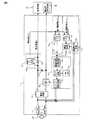
図1は、第1実施形態に係る電源回路の回路ブロック図である。(Configuration of the power supply circuit according to the first embodiment)
FIG. 1 is a circuit block diagram of a power supply circuit according to the first embodiment.
電源回路1は、開閉器11と、整流回路12と、平滑コンデンサ13と、負荷電流検出回路14と、スイッチング回路15と、第1比較回路16と、第2比較回路17と、過電流制御回路18とを有する。電源回路1は、商用電源90から入力された交流を直流に変換し、変換した直流を負荷回路91に供給する。負荷回路91は、遊技機に設けられ、電源回路1から供給される電力により不図示の表示装置等を制御して種々の演出を実行する演出用制御回路92を含む種々の電気回路及び電子機器等を含む。 The
開閉器11は、一例では電磁開閉器であり、一端が接続される商用電源90と、他端が接続される整流回路12等との間の電気的接続を入切する。開閉器11は、投入されると、商用電源90から整流回路12等に交流を供給する。開閉器11は、開放されると、商用電源90から整流回路12等への交流の供給を停止する。整流回路12は、商用電源90から入力される交流を整流して平滑回路4に出力する。整流回路12は、一例ではブリッジ整流回路であり、他の例では全波同期整流回路である。平滑コンデンサ13は、整流回路12から入力された電流を平滑化して負荷電流ILを負荷回路91に供給する。The switch 11 is an electromagnetic switch in one example, and turns on and off the electrical connection between the
負荷電流検出回路14は、検出抵抗素子19と、増幅回路20とを有し、平滑コンデンサ13と負荷回路91との間に配置される。検出抵抗素子19は、平滑コンデンサ13と負荷回路91との間に接続され、整流回路12から平滑コンデンサ13を介して負荷回路91に流れる負荷電流ILに応じた電圧を増幅回路20に出力する。増幅回路20は、電流検出アンプ又は電流センスアンプとも称され、検出抵抗素子19から入力された電圧を増幅した検出電圧VDを第1比較回路16及び第2比較回路17に出力する。増幅回路20は、一例では、差動増幅型のオペアンプである。The load
負荷電流検出回路14は、一例では、負荷電流ILが1Aであるときに、1Vの検出電圧VDを出力する。したがって、負荷電流ILが2Aであるときに検出電圧VDは2Vになり、負荷電流ILが10Aであるときに検出電圧VDは10Vになる。In one example, the load
スイッチング回路15は、整流回路12と負荷回路91との間に配置され、オン状態のときに整流回路12と負荷回路91との間を接続し、オフ状態のときに整流回路12と負荷回路91との間の接続を遮断する。スイッチング回路15は、一例ではソースが整流回路12に接続され、ドレインが負荷回路91に接続され且つゲートが過電流制御回路18に接続され、過電流制御回路18からの信号に応じてオン状態とオフ状態とを切り換えるnMOSFETを含む。また、スイッチング回路15は、他の例では過電流制御回路18からの信号に応じてオン状態とオフ状態とを切り換える継電器を含む。スイッチング回路15は、「Hi」の信号であるオン指示信号が過電流制御回路18から入力されるとオン状態になり、「Low」の信号であるオフ指示信号が過電流制御回路18から入力されるとオフ状態になる。 The switching
第1比較回路16は、第1コンパレータ21と、第1ダイオード22とを有し、負荷電流ILに応じた検出電圧VDと第1閾値電圧VTH1とを比較して、検出電圧VDが第1閾値電圧VTH1以上であるときに、第1過電流信号を出力する。第1コンパレータ21は、一方の入力端子に増幅回路20から負荷電流ILに応じた検出電圧VDが入力され、他方の入力端子には第1閾値電圧VTH1が入力される。第1閾値電圧VTH1は、一例ではエミッタフォロア回路等の定電圧源により生成される。第1コンパレータ21の出力端子からは、検出電圧VDが第1閾値電圧VTH1よりも低いときに「Low」の信号が出力され、検出電圧VDが第1閾値電圧VTH1以上であるときに「Hi」の信号である第1過電流信号が出力される。第1ダイオード22は、アノードが第1コンパレータ21の出力端子に接続され、第1コンパレータ21の出力端子から出力される信号をカソードから出力する。The
第2比較回路17は、第2コンパレータ31と、起動計時回路32と、出力無効回路33と、第2ダイオード34とを有する。第2比較回路17は、負荷電流ILに応じた検出電圧VDと第1閾値電圧VTH1よりも低い第2閾値電圧VTH2とを比較して、電源回路1が起動したから所定の起動時間が経過する間に検出電圧VDが第2閾値電圧VTH2以上であるときに、第2過電流信号を出力する。The
第2コンパレータ31は、一方の入力端子に増幅回路20から負荷電流ILに応じた検出電圧VDが入力され、他方の入力端子には第2閾値電圧VTH2が入力される。第2閾値電圧VTH2は、第1閾値電圧VTH1よりも低い電圧であり、一例では第1閾値電圧VTH1と同様にエミッタフォロア回路等の定電圧源により生成される。第2コンパレータ31の出力端子からは、検出電圧VDが第2閾値電圧VTH2よりも低いときに「Low」の信号が出力され、検出電圧VDが第2閾値電圧VTH2以上であるときに「Hi」の信号である第2過電流信号が出力される。In the second comparator 31, the detection voltage VD corresponding to the load current IL is input from the
起動計時回路32は、一例ではRC回路等の時定数回路を有し、開閉器11と接続される。起動計時回路32は、開閉器11が投入されて、商用電源90から開閉器11を介して交流が入力されると、計時動作を開始する。起動計時回路32は、交流の入力に応じて計時動作を開始することにより、商用電源90と整流回路12との間を接続されたときからの時間を計時する。起動計時回路32は、商用電源90と整流回路12との間を接続されたときから所定の起動時間が経過したときに、計時した時間が所定の起動時間を経過したことを示す起動時間経過信号を出力無効回路33に出力する。起動時間は一例では2秒である。出力無効回路33は、起動計時回路32から起動時間経過信号が入力されていないとき、第2コンパレータ31の出力端子から出力される信号を第2ダイオード34のアノードに出力する。また、出力無効回路33は、起動計時回路32から起動時間経過信号が入力されているとき、第2コンパレータ31の出力端子から出力される信号にかかわらず「Low」の信号を第2ダイオード34のアノードに出力する。出力無効回路33は、一例ではゲートが起動計時回路32の出力端子に接続され、ソースが接地され、ドレインが第2コンパレータ31の出力端子及び第2ダイオード34のアノードに接続されたFETである。第2ダイオード34は、アノードが第2コンパレータ31及び出力無効回路33の出力端子に接続され、第1コンパレータ21の出力端子から出力される信号をカソードから出力する。 The
第1コンパレータ21の出力端子及び第2コンパレータ31の出力端子は、第1ダイオード22及び第2ダイオード34のそれぞれを介して過電流制御回路18の入力端子に共に接続される。検出電圧VDが第1閾値電圧VTH1よりも低く且つ第2閾値電圧VTH2よりも高いとき、第1コンパレータ21は「Low」の信号を出力し、第2コンパレータ31は「Hi」の信号を出力する。第1ダイオード22が逆バイアスになり順方向の電流を遮断して、第1ダイオード22のアノード側の電位は「Low」となり且つカソード側の電位が「Hi」となるため、過電流制御回路18の入力端子には「Hi」の信号が入力される。同様に、第2ダイオード34のアノード側の電位が「Low」となり且つ第1コンパレータ21が第1過電流信号である「Hi」の信号を出力するとき、第2ダイオード34が逆バイアスになり過電流制御回路18の入力端子には「Hi」の信号が入力される。The output terminal of the
過電流制御回路18は、継続時間計時回路41と、ラッチ回路42と、スイッチ制御回路43と、発光回路44とを有する。継続時間計時回路41は、一例ではRC回路等の時定数回路を有し、「Hi」の信号である第1過電流信号及び第2過電流信号の何れかが入力されたときからの時間を計時し、所定の継続時間が経過したときに、ラッチ回路42にトリガ信号を出力する。所定の継続時間は、一例では100ミリ秒であるが起動時に突入電流が流れるときに負荷電流ILに応じた検出電圧VDが第2閾値電圧VTH2以上である時間よりも長ければよい。すなわち、所定の継続時間は、突入電流が流れるときの負荷電流ILの大きさが第2閾値電圧VTH2に対応する第2閾値以上である時間よりも長ければよい。The
ラッチ回路42は、一例ではD端子に「Hi」の信号が入力され且つCK端子にトリガ信号が入力されるフリップフロップである。ラッチ回路42は、整流回路12に交流が入力されると、「Low」の信号をスイッチ制御回路43及び発光回路44に出力し、トリガ信号が入力されるまで「Low」の信号を出力し続ける。また、ラッチ回路42は、トリガ信号が入力されると出力する信号を「Low」から「Hi」に遷移させ、その後、整流回路12に交流が入力されなくなるまで「Hi」の信号を出力し続ける。 For example, the
スイッチ制御回路43は、開閉器11及びラッチ回路42に接続される。スイッチ制御回路43は、開閉器11を介して商用電源90から交流が入力され且つラッチ回路42から「Low」の信号が入力されるとき、「Hi」の信号であるオン指示信号をスイッチング回路15に出力する。また、スイッチ制御回路43は、商用電源90から交流が入力され且つラッチ回路42から「Hi」の信号が入力されるとき、「Low」の信号であるオフ指示信号をスイッチング回路15に出力する。 The
発光回路44は、一例ではLED素子を含み、ラッチ回路42から「Hi」の信号が入力されると発光して、負荷電流ILがレアショートに起因する過電流が含むおそれがあることを不図示のオペレータに表示する。Emitting
(第1実施形態に係る電源回路の動作)
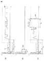
図2は、電源回路1の動作を示すタイミングチャートである。図2(a)はレアショートに起因する過電流が流れない状態を示す図であり、図2(b)は起動時にレアショートに起因する過電流が流れる状態を示す図であり、図2(c)は遊技機の定常動作時にレアショートに起因する過電流が流れる状態を示す図である。図2(a)〜2(c)において、横軸は経過時間を示し、縦軸は負荷電流ILを示す。また、図2(a)〜2(c)において、一点鎖線及び二点鎖線のそれぞれは、負荷電流ILがレアショートに起因する過電流を含むと電源回路1が判断してスイッチング回路15をオフ状態にする閾値を示す。一点鎖線は負荷電流ILに応じた検出電圧VDが第1閾値電圧VTH1を超える場合の第1閾値を示し、二点鎖線は負荷電流ILに応じた検出電圧VDが第2閾値電圧VTH2を超える場合の第2閾値を示す。波形201〜203は、それぞれの状態の負荷電流ILの一例を示す。(Operation of the power supply circuit according to the first embodiment)
FIG. 2 is a timing chart showing the operation of the
まず、図2(a)を参照してレアショート等に起因する過電流が流れない状態を説明する。図2(a)に示す状態では、電源回路1が起動してから遊技機の定常動作の間に亘って、負荷回路91にレアショートは発生しない。 First, with reference to FIG. 2A, a state in which an overcurrent caused by a rare short or the like does not flow will be described. In the state shown in FIG. 2A, a rare short circuit does not occur in the
開閉器11が投入されると、比較的大きな電流である突入電流が、t11の時間に亘って電源回路1の整流回路12から負荷回路91に流れる。開閉器11が投入されると、起動計時回路32は、計時動作を開始する。突入電流により負荷電流ILが二点鎖線で示される検出電圧VDが第2閾値電圧VTH2を超えることを示す閾値を超えると、第2コンパレータ31は、「Hi」の信号である第2過電流信号を、第2ダイオード34を介して継続時間計時回路41に出力する。継続時間計時回路41は、第2過電流信号が入力されると計時動作を開始する。しかしながら、t12で示される突入電流が閾値を超える時間は、一例が100ミリ秒である継続時間計時回路41が計時する継続時間よりも十分に短いので、継続時間計時回路41が継続時間まで計時する前に、検出電圧VDが第2閾値電圧VTH2よりも低くなる。検出電圧VDが第2閾値電圧VTH2よりも低くなると、第2コンパレータ31が第2過電流信号の出力を停止するので、継続時間計時回路41は、計時を終了する。When the switch 11 is turned on, a relatively a large current inrush current flows from the
開閉器11が投入されてからt13で示される起動時間が経過すると、起動計時回路32は出力無効回路33に起動時間経過信号を出力し、出力無効回路33は「Low」の信号を第2ダイオード34のアノードに出力する。出力無効回路33が「Low」の信号を第2ダイオード34のアノードに出力することにより、第2比較回路17は、負荷電流ILに応じた検出電圧VDにかかわらず第2ダイオード34のアノードの電圧は「Low」に固定される。第2ダイオード34のアノードの電圧が「Low」に固定されることにより、負荷電流ILに応じた検出電圧VDが第2閾値電圧VTH2以上になった場合でも、第2比較回路17は、第2過電流信号を出力しない。したがって、負荷電流ILの閾値は、一点鎖線で示される第1閾値に応じた電流に上昇する。When the activation time switch 11 are shown in t13 after being turned elapses, start counting
t14で示される時間が経過して負荷回路91が遊技機の動作制御を開始するまで、負荷回路91は電力をほとんど消費しないので、負荷電流ILは、矢印Aで示されるように比較的小さく且つ負荷電流ILの変動も小さい。t14で示される時間が経過して負荷回路91が遊技機の動作制御を開始すると、負荷電流ILは、矢印Aで示される起動時の消費電流よりも大きくなると共に、負荷電流ILの変動も大きくなる。to the
次に、図2(b)を参照して起動時にレアショートに起因する過電流が流れる状態を説明する。図2(b)に示す状態では、開閉器11が投入される前に負荷回路91の何れかでレアショートが発生している。 Next, with reference to FIG. 2 (b), a state in which an overcurrent caused by a rare short flows at the time of startup will be described. In the state shown in FIG. 2B, a rare short has occurred in any of the
開閉器11が投入されると、突入電流が、電源回路1の整流回路12から負荷回路91に流れる。このときの突入電流は、レアショートに起因する過電流を含むため、図2(a)に示す状態の突入電流よりも大きくなる。開閉器11が投入されると、起動計時回路32は、計時動作を開始する。次いで、突入電流により負荷電流ILが二点鎖線で示される検出電圧VDが第2閾値電圧VTH2であることを示す閾値以上になると、第2コンパレータ31は、「Hi」の信号である第2過電流信号を、第2ダイオード34を介して継続時間計時回路41に出力する。継続時間計時回路41は、第2過電流信号が入力されると計時動作を開始する。When the switch 11 is turned on, an inrush current flows from the
開閉器11が投入されてから、t21で示される時間を経過して突入電流が流れなくなっても、負荷電流ILは、レアショートに起因する過電流を含むため、二点鎖線で示される閾値以上になる。負荷電流ILが二点鎖線で示される閾値以上であるため、第2コンパレータ31は第2過電流信号の継続時間計時回路41への出力を継続し、継続時間計時回路41は計時を継続する。From switch 11 is turned on, even when no inrush current flows are passed the time represented by t21, the load current IL, to include an overcurrent due to short circuit, indicated by the two-dot chain line Be over threshold. Because the load current IL is equal to or greater than the threshold indicated by the two-dot chain line, the second comparator 31 continues to output to the continuation time measuring circuit 41 of the second over-current signal, the duration time counting circuit 41 continues the time measurement .
継続時間計時回路41は、t22で示される継続時間に亘って計時すると、ラッチ回路42にトリガ信号を出力する。ラッチ回路42は、トリガ信号が入力されると、スイッチ制御回路43及び発光回路44に出力する信号を「Low」から「Hi」に遷移させる。スイッチ制御回路43は、商用電源90から交流が入力され且つラッチ回路42から「Hi」の信号が入力されると、「Low」の信号であるオフ指示信号をスイッチング回路15に出力する。スイッチング回路15は、オフ指示信号が入力されるとオフ状態になり、整流回路12と負荷回路91との間の接続を遮断する。スイッチング回路15が整流回路12と負荷回路91との間の接続を遮断すると、負荷電流ILは流れなくなる。The continuation time counting circuit 41 outputs a trigger signal to the
次に、図2(c)を参照して遊技機の定常動作時にレアショートに起因する過電流が流れる状態を説明する。図2(c)に示す状態では、遊技機の定常動作の間に負荷回路91の何れかでレアショートが発生している。 Next, with reference to FIG. 2 (c), a state in which an overcurrent caused by a rare short flows during a steady operation of the gaming machine will be described. In the state shown in FIG. 2C, a rare short occurs in any of the
開閉器11が投入されてから遊技機が定常動作を開始するまでの動作は、図2(a)を参照して説明した動作と同様である。すなわち、図2(c)のt31〜t34は、図2(a)のt11〜t14のそれぞれに対応する。開閉器11が投入されてから遊技機が定常動作を開始するまでの動作は、図2(a)を参照して説明しているので、ここでは詳細な説明を省略する。The operation from when the switch 11 is turned on until the gaming machine starts a steady operation is the same as the operation described with reference to FIG. That is, t31 to t34 in FIG. 2C correspond to t11 to t14 in FIG. Since the operation from when the switch 11 is turned on until the gaming machine starts a steady operation has been described with reference to FIG. 2 (a), detailed description is omitted here.
矢印Bで示される時点で、レアショートが発生するとレアショートに起因する過電流を含むことにより、負荷電流ILが一点鎖線で示される検出電圧VDが第1閾値電圧VTH1であることを示す第1閾値以上になる。検出電圧VDが第1閾値電圧VTH1以上になると、第1コンパレータ21は、「Hi」の信号である第1過電流信号を、第1ダイオード22を介して継続時間計時回路41に出力する。継続時間計時回路41は、第2過電流信号が入力されると計時動作を開始する。When a rare short occurs at the time indicated by the arrow B, the detection voltage VD indicated by the one-dot chain line indicates that the load current IL is the first threshold voltage VTH1 by including an overcurrent caused by the rare short. It becomes more than the 1st threshold shown. When the detection voltage VD becomes equal to or higher than the first threshold voltage VTH1 , the
継続時間計時回路41は、t35で示される継続時間に亘って計時すると、ラッチ回路42にトリガ信号を出力する。ラッチ回路42は、トリガ信号が入力されると、スイッチ制御回路43及び発光回路44に出力する信号を「Low」から「Hi」に遷移させる。スイッチ制御回路43は、商用電源90から交流が入力され且つラッチ回路42から「Hi」の信号が入力されると、「Low」の信号であるオフ指示信号をスイッチング回路15に出力する。スイッチング回路15は、オフ指示信号が入力されるとオフ状態になり、整流回路12と負荷回路91との間の接続を遮断する。スイッチング回路15が整流回路12と負荷回路91との間の接続を遮断すると、負荷電流ILは流れなくなる。Continuation time measuring circuit 41, the counts over the duration represented by t35, and outputs a trigger signal to the
(第1実施形態に係る電源回路の作用効果)
第1実施形態に係る電源回路は、起動時に突入電流が流れる時間よりも長い継続時間に亘って連続して入力されたことを検出したときに、負荷回路への負荷電流の供給を停止するので、突入電流により負荷電流の供給を停止するおそれはない。第1実施形態に係る電源回路は、突入電流により負荷電流の供給を停止するおそれはないので、負荷電流の大きさ及び変動が比較的小さい起動時に負荷電流が正常であるか否かを判定することができる。第1実施形態に係る電源回路は、負荷電流の大きさ及び変動が比較的小さい起動時に負荷電流が正常であるか否かを判定することができるので、レアショートに起因する過電流等の比較的小さな異常電流も検出することができる。(Operational effect of the power supply circuit according to the first embodiment)
The power supply circuit according to the first embodiment stops the supply of the load current to the load circuit when it is detected that the input is continuously input for a duration longer than the time during which the inrush current flows during startup. There is no risk of stopping the supply of load current due to the inrush current. Since the power supply circuit according to the first embodiment has no fear of stopping the supply of the load current due to the inrush current, it is determined whether or not the load current is normal at start-up when the magnitude and fluctuation of the load current are relatively small. be able to. Since the power supply circuit according to the first embodiment can determine whether or not the load current is normal at the start-up when the magnitude and fluctuation of the load current are relatively small, comparison of overcurrent caused by a rare short-circuit is performed. A small abnormal current can be detected.
例えば、第1実施形態に係る電源回路において、起動時の負荷電流が1A未満であり、定常動作時の負荷電流が10A程度である場合、起動時の第2閾値電圧を1A以上の負荷電流が検出可能な値に設定することができる。これにより、起動時に負荷電流が1A以上流れるときに、異常電流であると判定して負荷回路への負荷電流の供給を停止できるので、レアショート等に起因する比較的小さな過電流による遊技機の発火を防止できる。 For example, in the power supply circuit according to the first embodiment, when the load current at start-up is less than 1 A and the load current at steady operation is about 10 A, the second threshold voltage at start-up is a load current of 1 A or more. It can be set to a detectable value. As a result, when the load current flows at 1 A or more at startup, it can be determined that the current is abnormal and the supply of the load current to the load circuit can be stopped. Can prevent ignition.
(第2実施形態に係る電源回路の構成)
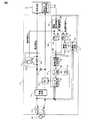
図3は、第2実施形態に係る電源回路の回路ブロック図である。(Configuration of Power Supply Circuit According to Second Embodiment)
FIG. 3 is a circuit block diagram of a power supply circuit according to the second embodiment.
第2実施形態に係る電源回路2は、閾値変更回路51を含む第1比較回路50が第1比較回路16の代わりに配置されることが、第1実施形態に係る電源回路1と相違する。第1比較回路50以外の電源回路2の構成素子は、同一符号が付された第1実施形態に係る電源回路1の構成素子と同様の構成及び機能を有するので、ここでは詳細な説明は省略する。 The
図4は、閾値変更回路51の内部回路ブロック図である。 FIG. 4 is an internal circuit block diagram of the threshold
閾値変更回路51は、入力端子52と、出力端子53と、スイッチングトランジスタ54と、第1抵抗素子55と、第2抵抗素子56と、第3抵抗素子57とを有する。閾値変更回路51は、演出用制御回路92から入力端子52に入力される状態判別信号に応じて、出力端子53から第1コンパレータ21に出力される第1閾値電圧VTH1の値を変更することができる。The threshold
演出用制御回路92は、第1状態判別信号及び第2状態判別信号の2つの状態判別信号を閾値変更回路51に出力する。演出用制御回路92は、遊技球が入賞口に入賞していない非入賞状態のときに第1状態判別信号を出力し、遊技球が入賞口に入賞して大当たり抽選などの、通常演出とは異なる特別演出が実行される入賞状態のときに第2状態判別信号を出力する。入賞状態の負荷電流ILは、不図示の表示装置等を制御して種々の特別演出が実行されるため、非入賞状態の負荷電流ILよりも大きくなると予測される。第1状態判別信号及び第2状態判別信号のそれぞれは、負荷電流ILの変動を予測する負荷予測信号である。The
スイッチングトランジスタ54は、バイポーラトランジスタであり、ベースが入力端子52に接続され、エミッタが電源電圧に接続され、コレクタが第1抵抗素子55の一端に接続される。スイッチングトランジスタ54は、演出用制御回路92から入力端子に第1状態判別信号が入力されるとき、ベース電流及びエミッタ電流を流さずにオフする。また、スイッチングトランジスタ54は、演出用制御回路92から入力端子に第2状態判別信号が入力されるとき、ベース電流及びエミッタ電流を流してオンする。第1抵抗素子55の他端は、第2抵抗素子56及び第3抵抗素子57の一端と共に出力端子53に接続される。第2抵抗素子56は他端が電源電圧に接続され、第3抵抗素子57は他端が接地される。閾値変更回路51では、スイッチングトランジスタ54がオンするときの第1閾値電圧は、第1抵抗素子55と第2抵抗素子56とが並列接続されることによりスイッチングトランジスタ54がするオフするときの第1閾値電圧VTH1よりも高くなる。The switching
(第2実施形態に係る電源回路の動作)
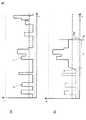
図5は、レアショート等に起因する過電流が流れない状態での電源回路2の動作を示すタイミングチャートである。レアショート等に起因する過電流が流れる状態の動作は、図2(b)及び図2(c)を参照して説明した電源回路1の動作と同様なのでここでは詳細な説明は省略する。図5において、横軸は経過時間を示し、縦軸は負荷電流ILを示す。また、図5において、一点鎖線及び二点鎖線のそれぞれは、負荷電流ILがレアショートに起因する過電流を含むと過電流制御回路18が判断してスイッチング回路15をオフ状態にする閾値を示す。一点鎖線は負荷電流ILに応じた検出電圧VDが第1閾値電圧VTH1を超える場合の第1閾値を示し、二点鎖線は負荷電流ILに応じた検出電圧VDが第2閾値電圧VTH2を超える場合の第2閾値を示す。波形501は、負荷電流ILの一例を示す。(Operation of the power supply circuit according to the second embodiment)
FIG. 5 is a timing chart showing the operation of the
開閉器11が投入されてから遊技機が定常動作を開始するまでの動作は、図2(a)を参照して説明した動作と同様である。すなわち、図5のt41〜t44は、図2(a)のt11〜t14のそれぞれに対応する。開閉器11が投入されてから遊技機が定常動作を開始するまでの動作は、図2(a)を参照して説明しているので、ここでは詳細な説明を省略する。The operation from when the switch 11 is turned on until the gaming machine starts a steady operation is the same as the operation described with reference to FIG. That is, t41 to t44 in FIG. 5 correspond to t11 to t14 in FIG. Since the operation from when the switch 11 is turned on until the gaming machine starts a steady operation has been described with reference to FIG. 2 (a), detailed description is omitted here.
開閉器11が投入されてからt43で示される起動時間が経過した矢印Cで示される時点において、起動計時回路32は出力無効回路33に起動時間経過信号を出力し、出力無効回路33は「Low」の信号を第2ダイオード34のアノードに出力する。これにより、図2(a)を参照して説明したように、負荷電流ILの閾値は、一点鎖線で示される第1閾値に応じた電流に上昇する。ここでは、遊技球が入賞口に入賞していないので、演出用制御回路92は、閾値変更回路51に第1状態判別信号を出力する。At the time indicated by the arrow C when the activation time indicated by t43 has elapsed since the switch 11 was turned on, the
矢印Dで示される時点で遊技球が入賞口に入賞したことを検出すると、演出用制御回路92は、閾値変更回路51に第2状態判別信号を出力する。閾値変更回路51のスイッチングトランジスタ54は、第2状態判別信号が入力されると、オンする。遊技球が入賞口に入賞したことに応じてスイッチングトランジスタ54がオンすることにより、第1閾値電圧VTH1は、入賞に伴う特別演出の実行により増加した負荷電流ILに応じて上昇する。When it is detected that the game ball has won the winning opening at the time indicated by the arrow D, the
(第2実施形態に係る電源回路の作用効果)
第2実施形態に係る電源回路は、遊技機の動作を制御する制御回路から遊技機の動作状態に応じた状態判別信号が入力される。第2実施形態に係る電源回路は、入力された状態判別信号に応じて定常動作時の過電流検出に使用される第1閾値電圧を変更することができる。第2実施形態に係る電源回路は、入力された状態判別信号に応じて第1閾値電圧を変更することにより、レアショートに起因する過電流等の比較的小さな異常電流の定常動作時の検出感度を向上させることができる。(Operational effect of the power supply circuit according to the second embodiment)
The power supply circuit according to the second embodiment receives a state determination signal corresponding to the operating state of the gaming machine from a control circuit that controls the operation of the gaming machine. The power supply circuit according to the second embodiment can change the first threshold voltage used for overcurrent detection during steady operation according to the input state determination signal. The power supply circuit according to the second embodiment changes the first threshold voltage according to the input state determination signal, thereby detecting sensitivity during steady operation of a relatively small abnormal current such as an overcurrent caused by a rare short. Can be improved.
例えば、第2実施形態に係る電源回路において、非入賞状態の負荷電流が2〜3A程度であり、入賞状態の負荷電流が10A程度である場合、非入賞状態の第1閾値電圧を5Aに対応する電圧に設定し、入賞状態の第1閾値電圧を13Aに対応する電圧に設定できる。これにより、入賞状態において負荷電流が5A以上流れるときに、異常電流であると判定して負荷回路への負荷電流の供給を停止できるので、レアショート等に起因する比較的小さな過電流による遊技機の発火を防止できる。 For example, in the power supply circuit according to the second embodiment, when the non-winning state load current is about 2 to 3 A and the winning state load current is about 10 A, the non-winning state first threshold voltage corresponds to 5 A. The first threshold voltage in the winning state can be set to a voltage corresponding to 13A. This makes it possible to determine that the current is abnormal and stop supplying the load current to the load circuit when the load current flows 5A or more in the winning state, so that the gaming machine with a relatively small overcurrent caused by a rare short or the like Can prevent ignition.
(第3実施形態に係る電源回路の構成)
図6は、第3実施形態に係る電源回路の回路ブロック図である。(Configuration of Power Supply Circuit According to Third Embodiment)
FIG. 6 is a circuit block diagram of a power supply circuit according to the third embodiment.
第3実施形態に係る電源回路3は、第3比較回路60が更に配置されることが、第1実施形態に係る電源回路1と相違する。第3比較回路60以外の電源回路2の構成素子は、同一符号が付された第1実施形態に係る電源回路1の構成素子と同様の構成及び機能を有するので、ここでは詳細な説明は省略する。 The
第3比較回路60は、第3コンパレータ61と、パルス生成回路62と、カウンタ63と、高電流状態判定回路64と、第3ダイオード65とを有する。第3比較回路60は、負荷電流検出回路14に接続され、負荷電流ILと第1閾値VTH1及び第2閾値VTH2と相違する第3閾値VTH3とを比較し、負荷電流ILが所定の連続時間に亘って第3閾値VTH3より大きいときに、第3過電流信号を出力する。第3コンパレータ61は、一方の入力端子に増幅回路20から負荷電流ILに応じた検出電圧VDが入力され、他方の入力端子には第3閾値電圧VTH3が入力される。第3閾値電圧VTH3は、第1閾値電圧VTH1よりも低く且つ第2閾値電圧VTH2よりも高く、一例ではエミッタフォロア回路等の定電圧源により生成される。第3コンパレータ61の出力端子からは、検出電圧VDが第3閾値電圧VTH3よりも高いときに「Low」の信号が出力され、検出電圧VDが第3閾値電圧VTH3以下であるときに「Hi」の信号であるリセット信号が出力される。The
パルス生成回路62は、一例ではRC回路等の時定数回路を有し、開閉器11に接続される。パルス生成回路62は、開閉器11を介して商用電源90から交流が入力される間、所定のパルス周期でパルス信号を生成し、出力する。所定のパルス周期は、一例では1秒である。カウンタ63は、第3コンパレータ61及びパルス生成回路62に接続され、パルス信号が入力されたカウント数を計数し、リセット信号が入力されたときにカウント数をリセットする。高電流状態判定回路64は、カウンタ63に接続される。高電流状態判定回路64は、カウンタ63が計数したカウント数が所定のカウント閾値と等しくなったときに、パルス生成回路62のパルス周期及びカウンタ63のカウント数の乗算で規定される連続時間に達したと判定する。高電流状態判定回路64は、パルス生成回路62のパルス周期及びカウンタ63のカウント数の乗算で規定される連続時間に達したと判定すると、「Hi」の信号である第3過電流信号を出力する。所定のカウント閾値は、一例では120である。第3ダイオード65は、アノードが高電流状態判定回路64の出力端子に接続され、高電流状態判定回路64の出力端子から出力される信号をカソードから継続時間計時回路41に出力する。 The
所定のパルス周期が1秒であり且つ所定のカウント閾値が120である場合を例に、第3比較回路60の動作を説明する。この場合、パルス生成回路62のパルス周期及びカウンタ63のカウント数の乗算で規定される連続時間は、120秒になる。第3比較回路60は、120秒間に亘って検出電圧VDが第3閾値電圧VTH3より大きい電圧を維持したときに、第3過電流信号を出力する。一方、120秒間の間に負荷電流ILの減少に応じて検出電圧VDが第3閾値電圧VTH3以下になったとき、第3比較回路60は、カウント数がリセットされるため、第3過電流信号を出力しない。The operation of the
(第3実施形態に係る電源回路の動作)
図7は、電源回路3の定常動作時の動作を示すタイミングチャートである。図7(a)はレアショートに起因する過電流が流れない状態を示す図であり、図7(b)は遊技機の定常動作時にレアショートに起因する過電流が流れる状態を示す図である。図7(a)〜7(b)において、横軸は経過時間を示し、縦軸は負荷電流ILを示す。また、図7(a)〜7(b)において、横軸に平行に延伸する一点鎖線、二点鎖線及び破線のそれぞれは、負荷電流ILがレアショートに起因する過電流を含むと電源回路2が判断してスイッチング回路15をオフ状態にする閾値を示す。一点鎖線は負荷電流ILに応じた検出電圧VDが第1閾値電圧VTH1を超える場合の第1閾値を示し、二点鎖線は負荷電流ILに応じた検出電圧VDが第2閾値電圧VTH2を超える場合の第2閾値を示す。また、鎖線は、負荷電流ILに応じた検出電圧VDが第3閾値電圧VTH2を超える場合の第3閾値を示す。波形701〜702は、それぞれの状態の負荷電流ILの一例を示す。(Operation of the power supply circuit according to the third embodiment)
FIG. 7 is a timing chart showing the operation of the
図7(a)に示す状態では、レアショートは発生しておらず、負荷電流ILは第1閾値と、第2閾値との間で遷移する。矢印E及びF等で示すように、負荷回路91の動作に応じて負荷電流ILが第3閾値を超える場合がある。しかしながら、負荷電流ILが第3閾値を超える時間は、第3比較回路60においてパルス生成回路62のパルス周期及びカウンタ63のカウント数の乗算で規定される連続時間に達していないため、第3比較回路60は、第3過電流信号を出力しない。In the state shown in FIG. 7 (a), layer short is not generated, load current IL transitions between the first threshold and the second threshold value. As indicated by arrows E and F, the load current IL may exceed the third threshold depending on the operation of the
図7(b)に示す状態では、矢印Gで示される時点でレアショートが発生する。レアショートが発生した後も、負荷電流ILは第1閾値と第2閾値との間で遷移するものの、t51で示される連続時間を経過に亘って第3閾値電圧VTH2より高電圧になる。第3比較回路60は、連続時間を経過に亘って負荷電流ILが第3閾値電圧VTH2より高電圧になると、第3過電流信号を過電流制御回路18の継続時間計時回路41に出力する。In the state shown in FIG. 7B, a rare short occurs at the time indicated by the arrow G. Even after the occurrence of the short-circuit, the load current IL changes between the first threshold value and the second threshold value. However, the load current IL becomes higher than the third threshold voltage VTH2 over the continuous time indicated by t51. Become. When the load current IL becomes higher than the third threshold voltage VTH2 over a continuous time, the
継続時間計時回路41は、t52で示される継続時間に亘って計時すると、ラッチ回路42にトリガ信号を出力する。ラッチ回路42は、トリガ信号が入力されると、スイッチ制御回路43及び発光回路44に出力する信号を「Low」から「Hi」に遷移させる。スイッチ制御回路43は、商用電源90から交流が入力され且つラッチ回路42から「Hi」の信号が入力されると、「Low」の信号であるオフ指示信号をスイッチング回路15に出力する。スイッチング回路15は、オフ指示信号が入力されるとオフ状態になり、整流回路12と負荷回路91との間の接続を遮断する。スイッチング回路15が整流回路12と負荷回路91との間の接続を遮断すると、負荷電流ILは流れなくなる。The continuation time counting circuit 41 outputs a trigger signal to the
(第3実施形態に係る電源回路の作用効果)
第3実施形態に係る電源回路は、遊技機の負荷電流が、定常動作時に常に変動し、数分から十数分程度の期間の間に必ず負荷電流が減少する時点があることを利用する。すなわち、第3実施形態に係る電源回路は、遊技機の定常動作時の負荷電流が所定の連続時間に亘って第3閾値より大きいときに、負荷電流がレアショートに起因する過電流を含むと判定する。これにより、第3実施形態に係る電源回路は、定常動作時の異常電流の検出感度を向上させることができる。(Operational effect of the power supply circuit according to the third embodiment)
The power supply circuit according to the third embodiment utilizes the fact that the load current of the gaming machine constantly fluctuates during steady operation, and the load current always decreases during a period of several minutes to tens of minutes. That is, the power supply circuit according to the third embodiment includes an overcurrent caused by a rare short when the load current during the steady operation of the gaming machine is larger than the third threshold over a predetermined continuous time. judge. Thereby, the power supply circuit according to the third embodiment can improve the detection sensitivity of abnormal current during steady operation.
例えば、非入賞状態のときの負荷電流が2〜3A程度であり、入賞状態のときの負荷電流が10A程度である場合、第3閾値電圧を3Aに対応する電圧に設定し、連続時間が120秒になるようにパルス期間及びカウント数を設定できる。このように第3閾値電圧、パルス期間及びカウント数を設定することにより、120秒の連続時間に亘って3Aより大きい電流が流れるときに、負荷電流がレアショートに起因する過電流を含むと判定することができる。 For example, when the load current in the non-winning state is about 2 to 3 A and the load current in the winning state is about 10 A, the third threshold voltage is set to a voltage corresponding to 3 A, and the continuous time is 120 The pulse period and count number can be set to be seconds. By setting the third threshold voltage, the pulse period, and the number of counts in this way, when a current greater than 3 A flows over a continuous time of 120 seconds, it is determined that the load current includes an overcurrent caused by a rare short circuit. can do.
(実施形態に係る検出装置の変形例)
電源回路1〜3では、第1過電流信号〜第3過電流信号の何れも継続時間計時回路41を介してラッチ回路42に出力されるが、第1過電流信号及び第3過電流信号は継続時間計時回路41を介さずにラッチ回路42に直接出力されてもよい。(Modification of Detection Device According to Embodiment)
In the
第2実施形態に係る電源回路2では、閾値変更回路51は、演出用制御回路92から入力される状態判別信号に応じて第1閾値電圧を2つの電圧レベルの間で切替えるが、実施形態に係る電源回路では、第1閾値電圧を3つ以上の電圧レベルの間で切替えてもよい。 In the
(実施形態に係る電源回路の遊技機への搭載例)
上記の実施形態又は変形例に係る電源回路は、弾球遊技機又は回胴遊技機といった遊技機に搭載されてもよい。(Example of mounting the power supply circuit according to the embodiment on a gaming machine)
The power supply circuit according to the above-described embodiment or modification may be mounted on a gaming machine such as a ball game machine or a spinning game machine.
図8は、上記の実施形態又は変形例に係る電源回路を備えた弾球遊技機100の概略斜視図である。また図9は、弾球遊技機100の概略背面図である。図8に示すように、弾球遊技機100は、上部から中央部の大部分の領域に設けられ、遊技機本体である遊技盤101と、遊技盤101の下方に配設された球受け部102と、ハンドルを備えた操作部103と、遊技盤101の略中央に設けられた表示装置104とを有する。 FIG. 8 is a schematic perspective view of the
また弾球遊技機100は、遊技の演出のために、遊技盤101の前面において遊技盤101の下方に配置された固定役物部105と、遊技盤101と固定役物部105との間に配置された可動役物部106とを有する。また遊技盤101の側方にはレール107が配設されている。また遊技盤101上には不図示の多数の障害釘及び少なくとも一つの入賞装置108が設けられている。 Further, the
操作部103は、遊技者の操作によるハンドルの回動量に応じて図示しない発射装置より所定の力で遊技球を発射する。発射された遊技球は、レール107に沿って上方へ移動し、多数の障害釘の間を落下する。そして遊技球が何れかの入賞装置108に入ったことを、図示しないセンサにより検知すると、遊技盤101の背面に設けられた主制御回路110は、遊技球が入った入賞装置108に応じた所定個の遊技球を不図示の玉払い出し装置を介して球受け部102へ払い出す。更に主制御回路110は、遊技盤101の背面に設けられた演出用制御回路111を介して表示装置104に様々な映像を表示させる。 The
可動役物部106は、遊技の状態に応じて移動する可動体の一例であり、遊技盤101の背面に設けられた、可動体駆動装置112により駆動される。なお、遊技機100が、可動役物部106以外にも可動体を有する場合、例えば、入賞装置108の開口部に、開口の大きさを可変にする可動体を有する場合、その可動体も、可動体駆動装置112によって駆動されてもよい。 The movable
上記の実施形態又はその変形例に係る電源回路113は、主制御回路110、演出用制御回路111、可動体駆動装置112、表示装置104、発射装置及び玉払い出し装置など、供給された電力を利用して動作する遊技機の各負荷回路へ電力を供給する。 The
このように、当業者は、本発明の範囲内で、実施される形態に合わせて様々な変更を行うことができる。 As described above, those skilled in the art can make various modifications in accordance with the embodiment to be implemented within the scope of the present invention.
1〜3、113 電源回路
11 開閉器
12 整流回路
13 平滑コンデンサ
14 負荷電流検出回路
15 スイッチング回路
16 第1比較回路
17 第2比較回路
18 過電流制御回路
60 第3比較回路
90 商用電源
91 負荷回路
92、111 演出用制御回路
100 弾球遊技機(遊技機)1-3, 113 Power supply circuit 11
Claims (6)
Translated fromJapanese入力された交流を直流に変換する整流回路と、
オン状態のときに前記整流回路と前記負荷回路との間を接続し、オフ状態のときに前記整流回路と前記負荷回路との間の接続を遮断するスイッチング回路と、
前記スイッチング回路がオン状態のときに前記整流回路から前記負荷回路に流れる負荷電流を検出する負荷電流検出回路と、
前記負荷電流検出回路に接続され、前記負荷電流が前記第1閾値以上であるときに、第1過電流信号を出力する第1比較回路と、
前記負荷電流検出回路に接続され、前記交流が前記整流回路に入力されてから所定の起動時間が経過するまでの間に前記負荷電流が前記第1閾値よりも小さい第2閾値以上であるときに、第2過電流信号を出力する第2比較回路と、
前記負荷電流検出回路に接続され、前記負荷電流と、前記負荷電流が所定の連続時間に亘って前記第1閾値よりも小さく且つ前記第2閾値よりも大きい第3閾値より大きいときに、第3過電流信号を出力する第3比較回路と、
前記第1比較回路、前記第2比較回路及び前記第3比較回路に接続され、前記第1過電流信号又は前記第3過電流信号が入力されたこと、若しくは前記第2過電流信号が所定の継続時間に亘って連続して入力されたことに応じて、前記スイッチング回路をオフ状態にする過電流制御回路と、
を有することを特徴とする電源回路。A power supply circuit for supplying power to a load circuit provided in a gaming machine,
A rectifier circuit that converts input alternating current into direct current;
A switching circuit that connects between the rectifier circuit and the load circuit when in an on state, and that interrupts a connection between the rectifier circuit and the load circuit when in an off state;
A load current detection circuit for detecting a load current flowing from the rectifier circuit to the load circuit when the switching circuit is in an on state;
A first comparison circuit connected to the load current detection circuit and outputting a first overcurrent signal when the load current is equal to or greater than the first threshold;
When the load current is greater than or equal to a second threshold value that is smaller than the first threshold value and is connected to the load current detection circuit and before a predetermined start-up time elapses after the alternating current is input to the rectifier circuit A second comparison circuit for outputting a second overcurrent signal;
Connected to the load current detection circuit, and when the load current and the load current are larger than a third threshold that is smaller than the first threshold and larger than the second threshold over a predetermined continuous time, A third comparison circuit for outputting an overcurrent signal;
Connected to the first comparison circuit, the second comparison circuit, and the third comparison circuit, the first overcurrent signal or the third overcurrent signal is input, or the second overcurrent signal is a predetermined value An overcurrent control circuit that turns off the switching circuit in response to continuous input over a continuous time;
A power supply circuit comprising:
前記第1比較回路及び前記第2比較回路に接続され、前記第1過電流信号又は前記第2過電流信号の入力が継続する時間を計時する継続時間計時回路と、
前記継続時間計時回路に接続され、前記継続時間計時回路が計時した時間が前記継続時間に達したときに、前記オフ状態にすることを示すオフ指示信号を前記スイッチング回路に出力するスイッチ制御回路と、
を有する、請求項1に記載の電源回路。The overcurrent control circuit includes:
A duration measuring circuit that is connected to the first comparison circuit and the second comparison circuit and counts a time during which the input of the first overcurrent signal or the second overcurrent signal continues;
A switch control circuit that is connected to the duration time counting circuit and outputs an off instruction signal to the switching circuit indicating that the state is to be turned off when the time counted by the duration time counting circuit reaches the duration time; ,
The power supply circuit according to claim 1, comprising:
前記負荷電流の変動を予測する負荷予測信号が入力されたことに応じて、前記第1閾値に対応する第1閾値電圧を変更する閾値変更回路と、
前記負荷電流に対応する検出電圧と前記第1閾値電圧とを比較し、前記検出電圧が前記第1閾値電圧以上のときに第1過電流信号を出力する第1コンパレータと、
を有する、請求項1又は2に記載の電源回路。The first comparison circuit includes:
A threshold value changing circuit for changing a first threshold voltage corresponding to the first threshold value in response to an input of a load prediction signal for predicting fluctuations in the load current;
A first comparator that compares a detection voltage corresponding to the load current with the first threshold voltage and outputs a first overcurrent signal when the detection voltage is equal to or higher than the first threshold voltage;
The power supply circuit according to claim 1, comprising:
前記負荷電流に対応する検出電圧と前記第2閾値に対応する第2閾値電圧とを比較し、前記検出電圧が前記第2閾値電圧以上のときに第2過電流信号を出力する第2コンパレータと、
前記整流回路に前記交流が入力されてからの時間を計時し、計時した時間が前記起動時間を経過したときに、起動時間経過信号を出力する起動時間計時回路と、
前記第2コンパレータ及び前記起動時間計時回路に接続され、前記起動時間経過信号が入力される前に、前記第2過電流信号が入力されたときに、前記第2過電流信号を出力し、前記起動時間経過信号が入力された後に、前記第2過電流信号が入力されたときに、前記第2過電流信号を出力しない無効化回路と、
を有する、請求項1〜3の何れか一項に記載の電源回路。The second comparison circuit includes:
A second comparator that compares a detection voltage corresponding to the load current with a second threshold voltage corresponding to the second threshold and outputs a second overcurrent signal when the detection voltage is equal to or higher than the second threshold voltage; ,
A start-up time counting circuit that outputs a start-up time elapsed signal when the time elapsed since the alternating current is input to the rectifier circuit, and when the measured time has passed the start-up time;
The second overcurrent signal is output when the second overcurrent signal is input before the start time elapse signal is input, and is connected to the second comparator and the start time measuring circuit. An invalidation circuit that does not output the second overcurrent signal when the second overcurrent signal is input after the start time elapsed signal is input;
The power supply circuit according to claim 1, comprising:
前記負荷電流に対応する検出電圧と前記第3閾値に対応する第3閾値電圧とを比較し、前記検出電圧が前記第3閾値電圧以下のときにリセット信号を出力する第3コンパレータと、
所定のパルス周期でパルス信号を出力するパルス生成回路と、
前記第3コンパレータ及び前記パルス生成回路に接続され、前記パルス信号が入力されたカウント数を計数し、前記リセット信号が入力されたときに前記カウント数をリセットするカウンタと、
前記カウンタに接続され、前記カウント数が所定のカウント閾値と等しくなったときに、前記第3過電流信号を出力する高電流状態判定回路と、
を有する、請求項1〜4の何れか一項に記載の電源回路。The third comparison circuit includes:
A third comparator that compares a detection voltage corresponding to the load current with a third threshold voltage corresponding to the third threshold, and outputs a reset signal when the detection voltage is equal to or lower than the third threshold voltage;
A pulse generation circuit that outputs a pulse signal at a predetermined pulse period;
A counter that is connected to the third comparator and the pulse generation circuit, counts the count number when the pulse signal is input, and resets the count number when the reset signal is input;
A high current state determination circuit that is connected to the counter and outputs the third overcurrent signal when the count number becomes equal to a predetermined count threshold;
The power supply circuit according to claim 1, comprising:
前記負荷回路に電力を供給する電源回路であって、
入力された交流を直流に変換する整流回路と、
オン状態のときに前記整流回路と前記負荷回路との間を接続し、オフ状態のときに前記整流回路と前記負荷回路との間の接続を遮断するスイッチング回路と、
前記スイッチング回路がオン状態のときに前記整流回路から前記負荷回路に流れる負荷電流を検出する負荷電流検出回路と、
前記負荷電流検出回路に接続され、前記負荷電流が前記第1閾値以上であるときに、第1過電流信号を出力する第1比較回路と、
前記負荷電流検出回路に接続され、前記交流が前記整流回路に入力されてから所定の起動時間が経過するまでの間に前記負荷電流が前記第1閾値よりも小さい第2閾値以上であるときに、第2過電流信号を出力する第2比較回路と、
前記負荷電流検出回路に接続され、前記負荷電流と、前記負荷電流が所定の連続時間に亘って前記第1閾値よりも小さく且つ前記第2閾値よりも大きい第3閾値より大きいときに、第3過電流信号を出力する第3比較回路と、
前記第1比較回路、前記第2比較回路及び前記第3比較回路に接続され、前記第1過電流信号又は前記第3過電流信号が入力されたこと、若しくは前記第2過電流信号が所定の継続時間に亘って連続して入力されたことに応じて、前記スイッチング回路をオフ状態にする過電流制御回路と、を有する電源回路と、
を有することを特徴とする遊技機。A load circuit;
A power supply circuit for supplying power to the load circuit,
A rectifier circuit that converts input alternating current into direct current;
A switching circuit that connects between the rectifier circuit and the load circuit when in an on state, and that interrupts a connection between the rectifier circuit and the load circuit when in an off state;
A load current detection circuit for detecting a load current flowing from the rectifier circuit to the load circuit when the switching circuit is in an on state;
A first comparison circuit connected to the load current detection circuit and outputting a first overcurrent signal when the load current is equal to or greater than the first threshold;
When the load current is greater than or equal to a second threshold value that is smaller than the first threshold value and is connected to the load current detection circuit and before a predetermined start-up time elapses after the alternating current is input to the rectifier circuit A second comparison circuit for outputting a second overcurrent signal;
Connected to the load current detection circuit, and when the load current and the load current are larger than a third threshold that is smaller than the first threshold and larger than the second threshold over a predetermined continuous time, A third comparison circuit for outputting an overcurrent signal;
Connected to the first comparison circuit, the second comparison circuit, and the third comparison circuit, the first overcurrent signal or the third overcurrent signal is input, or the second overcurrent signal is a predetermined value A power supply circuit having an overcurrent control circuit that turns off the switching circuit in response to being continuously input over a duration time;
A gaming machine characterized by comprising:
Priority Applications (1)
| Application Number | Priority Date | Filing Date | Title |
|---|---|---|---|
| JP2015120643AJP6507871B2 (en) | 2015-06-15 | 2015-06-15 | Power supply circuit and game machine |
Applications Claiming Priority (1)
| Application Number | Priority Date | Filing Date | Title |
|---|---|---|---|
| JP2015120643AJP6507871B2 (en) | 2015-06-15 | 2015-06-15 | Power supply circuit and game machine |
Publications (2)
| Publication Number | Publication Date |
|---|---|
| JP2017005948Atrue JP2017005948A (en) | 2017-01-05 |
| JP6507871B2 JP6507871B2 (en) | 2019-05-08 |
Family
ID=57754547
Family Applications (1)
| Application Number | Title | Priority Date | Filing Date |
|---|---|---|---|
| JP2015120643AActiveJP6507871B2 (en) | 2015-06-15 | 2015-06-15 | Power supply circuit and game machine |
Country Status (1)
| Country | Link |
|---|---|
| JP (1) | JP6507871B2 (en) |
Cited By (2)
| Publication number | Priority date | Publication date | Assignee | Title |
|---|---|---|---|---|
| JP2020103691A (en)* | 2018-12-28 | 2020-07-09 | 株式会社平和 | Game machine |
| CN111937287A (en)* | 2018-10-31 | 2020-11-13 | 富士电机株式会社 | Integrated circuit and power supply circuit |
Citations (5)
| Publication number | Priority date | Publication date | Assignee | Title |
|---|---|---|---|---|
| JPS6046711A (en)* | 1983-08-20 | 1985-03-13 | 株式会社ピーエフユー | Overcurrent protecting system |
| US20020118500A1 (en)* | 2001-02-27 | 2002-08-29 | International Business Machines Corporation | Solid state circuit breaker with current overshoot protection |
| JP2004032641A (en)* | 2002-06-28 | 2004-01-29 | Yazaki Corp | Semiconductor switch device |
| JP2011109159A (en)* | 2009-11-12 | 2011-06-02 | Anden | Switching circuit having overcurrent detection function |
| JP2014008130A (en)* | 2012-06-28 | 2014-01-20 | Newgin Co Ltd | Game machine |
- 2015
- 2015-06-15JPJP2015120643Apatent/JP6507871B2/enactiveActive
Patent Citations (5)
| Publication number | Priority date | Publication date | Assignee | Title |
|---|---|---|---|---|
| JPS6046711A (en)* | 1983-08-20 | 1985-03-13 | 株式会社ピーエフユー | Overcurrent protecting system |
| US20020118500A1 (en)* | 2001-02-27 | 2002-08-29 | International Business Machines Corporation | Solid state circuit breaker with current overshoot protection |
| JP2004032641A (en)* | 2002-06-28 | 2004-01-29 | Yazaki Corp | Semiconductor switch device |
| JP2011109159A (en)* | 2009-11-12 | 2011-06-02 | Anden | Switching circuit having overcurrent detection function |
| JP2014008130A (en)* | 2012-06-28 | 2014-01-20 | Newgin Co Ltd | Game machine |
Cited By (3)
| Publication number | Priority date | Publication date | Assignee | Title |
|---|---|---|---|---|
| CN111937287A (en)* | 2018-10-31 | 2020-11-13 | 富士电机株式会社 | Integrated circuit and power supply circuit |
| JP2020103691A (en)* | 2018-12-28 | 2020-07-09 | 株式会社平和 | Game machine |
| JP7261581B2 (en) | 2018-12-28 | 2023-04-20 | 株式会社平和 | game machine |
Also Published As
| Publication number | Publication date |
|---|---|
| JP6507871B2 (en) | 2019-05-08 |
Similar Documents
| Publication | Publication Date | Title |
|---|---|---|
| TWI495891B (en) | Methods for operating state of charge indicators for battery packs, indicating circuits and monitoring circuits thereof | |
| US10181785B2 (en) | Power supply system and short circuit and/or bad connection detection method thereof, and power converter thereof | |
| US6590757B2 (en) | Method and apparatus for detecting and suppressing a parallel arc fault | |
| EP1150410A2 (en) | Solid state protection circuit for electrical apparatus | |
| CA2584556A1 (en) | Discharge lamp lighting device, and lighting equipment and lighting system using the device | |
| KR102352308B1 (en) | Wake-up apparatus of battery management system | |
| RU2014133901A (en) | POWER SUPPLY DEVICE | |
| KR20130142909A (en) | Short sensing circuit, short sensing method and power supply device comprising the short sensing circuit | |
| JP6442306B2 (en) | Fluid device | |
| RU2423770C2 (en) | Electric power tool with device of shut-off delay | |
| JP6507871B2 (en) | Power supply circuit and game machine | |
| JP6507872B2 (en) | Power supply circuit and game machine | |
| US9653931B2 (en) | Battery protection device and operation method thereof | |
| US20070139847A1 (en) | Power tool with circuit protection capability | |
| KR101259657B1 (en) | Semiconductor device and rechargeable power supply unit | |
| JP5524096B2 (en) | Overcurrent protection device | |
| JP3113309B2 (en) | Switch input circuit | |
| JP2006067776A5 (en) | ||
| JP2013143818A (en) | Semiconductor fuse device | |
| JP2018133923A (en) | Power supply device and game machine | |
| EP2633889A2 (en) | Power-saving control module for a body training machine | |
| JP5291527B2 (en) | Charging circuit | |
| KR200266980Y1 (en) | Electric Solder with Automatic Power Off | |
| CN219554573U (en) | Overcurrent time-delay protection circuit | |
| JP2013201807A (en) | Converter device |
Legal Events
| Date | Code | Title | Description |
|---|---|---|---|
| A621 | Written request for application examination | Free format text:JAPANESE INTERMEDIATE CODE: A621 Effective date:20180412 | |
| A977 | Report on retrieval | Free format text:JAPANESE INTERMEDIATE CODE: A971007 Effective date:20190121 | |
| A131 | Notification of reasons for refusal | Free format text:JAPANESE INTERMEDIATE CODE: A131 Effective date:20190129 | |
| A521 | Request for written amendment filed | Free format text:JAPANESE INTERMEDIATE CODE: A523 Effective date:20190207 | |
| A521 | Request for written amendment filed | Free format text:JAPANESE INTERMEDIATE CODE: A523 Effective date:20190222 | |
| TRDD | Decision of grant or rejection written | ||
| A01 | Written decision to grant a patent or to grant a registration (utility model) | Free format text:JAPANESE INTERMEDIATE CODE: A01 Effective date:20190305 | |
| A61 | First payment of annual fees (during grant procedure) | Free format text:JAPANESE INTERMEDIATE CODE: A61 Effective date:20190318 | |
| R150 | Certificate of patent or registration of utility model | Ref document number:6507871 Country of ref document:JP Free format text:JAPANESE INTERMEDIATE CODE: R150 | |
| R250 | Receipt of annual fees | Free format text:JAPANESE INTERMEDIATE CODE: R250 |