JP2017003744A - Optical device and image display device - Google Patents
Optical device and image display deviceDownload PDFInfo
- Publication number
- JP2017003744A JP2017003744AJP2015116897AJP2015116897AJP2017003744AJP 2017003744 AJP2017003744 AJP 2017003744AJP 2015116897 AJP2015116897 AJP 2015116897AJP 2015116897 AJP2015116897 AJP 2015116897AJP 2017003744 AJP2017003744 AJP 2017003744A
- Authority
- JP
- Japan
- Prior art keywords
- coil
- permanent magnet
- optical device
- conducting wire
- light
- Prior art date
- Legal status (The legal status is an assumption and is not a legal conclusion. Google has not performed a legal analysis and makes no representation as to the accuracy of the status listed.)
- Pending
Links
Images


Classifications
- G—PHYSICS
- G02—OPTICS
- G02B—OPTICAL ELEMENTS, SYSTEMS OR APPARATUS
- G02B26/00—Optical devices or arrangements for the control of light using movable or deformable optical elements
- G02B26/08—Optical devices or arrangements for the control of light using movable or deformable optical elements for controlling the direction of light
- G02B26/0816—Optical devices or arrangements for the control of light using movable or deformable optical elements for controlling the direction of light by means of one or more reflecting elements
- G02B26/0833—Optical devices or arrangements for the control of light using movable or deformable optical elements for controlling the direction of light by means of one or more reflecting elements the reflecting element being a micromechanical device, e.g. a MEMS mirror, DMD
- G02B26/085—Optical devices or arrangements for the control of light using movable or deformable optical elements for controlling the direction of light by means of one or more reflecting elements the reflecting element being a micromechanical device, e.g. a MEMS mirror, DMD the reflecting means being moved or deformed by electromagnetic means
- G—PHYSICS
- G02—OPTICS
- G02B—OPTICAL ELEMENTS, SYSTEMS OR APPARATUS
- G02B27/00—Optical systems or apparatus not provided for by any of the groups G02B1/00 - G02B26/00, G02B30/00
- G02B27/01—Head-up displays
- G02B27/0101—Head-up displays characterised by optical features
- G—PHYSICS
- G02—OPTICS
- G02B—OPTICAL ELEMENTS, SYSTEMS OR APPARATUS
- G02B27/00—Optical systems or apparatus not provided for by any of the groups G02B1/00 - G02B26/00, G02B30/00
- G02B27/01—Head-up displays
- G02B27/017—Head mounted
- G02B27/0172—Head mounted characterised by optical features
- G—PHYSICS
- G03—PHOTOGRAPHY; CINEMATOGRAPHY; ANALOGOUS TECHNIQUES USING WAVES OTHER THAN OPTICAL WAVES; ELECTROGRAPHY; HOLOGRAPHY
- G03B—APPARATUS OR ARRANGEMENTS FOR TAKING PHOTOGRAPHS OR FOR PROJECTING OR VIEWING THEM; APPARATUS OR ARRANGEMENTS EMPLOYING ANALOGOUS TECHNIQUES USING WAVES OTHER THAN OPTICAL WAVES; ACCESSORIES THEREFOR
- G03B21/00—Projectors or projection-type viewers; Accessories therefor
- G03B21/14—Details
- G03B21/142—Adjusting of projection optics
- G—PHYSICS
- G03—PHOTOGRAPHY; CINEMATOGRAPHY; ANALOGOUS TECHNIQUES USING WAVES OTHER THAN OPTICAL WAVES; ELECTROGRAPHY; HOLOGRAPHY
- G03B—APPARATUS OR ARRANGEMENTS FOR TAKING PHOTOGRAPHS OR FOR PROJECTING OR VIEWING THEM; APPARATUS OR ARRANGEMENTS EMPLOYING ANALOGOUS TECHNIQUES USING WAVES OTHER THAN OPTICAL WAVES; ACCESSORIES THEREFOR
- G03B5/00—Adjustment of optical system relative to image or object surface other than for focusing
- G03B5/02—Lateral adjustment of lens
- G—PHYSICS
- G09—EDUCATION; CRYPTOGRAPHY; DISPLAY; ADVERTISING; SEALS
- G09G—ARRANGEMENTS OR CIRCUITS FOR CONTROL OF INDICATING DEVICES USING STATIC MEANS TO PRESENT VARIABLE INFORMATION
- G09G3/00—Control arrangements or circuits, of interest only in connection with visual indicators other than cathode-ray tubes
- G09G3/001—Control arrangements or circuits, of interest only in connection with visual indicators other than cathode-ray tubes using specific devices not provided for in groups G09G3/02 - G09G3/36, e.g. using an intermediate record carrier such as a film slide; Projection systems; Display of non-alphanumerical information, solely or in combination with alphanumerical information, e.g. digital display on projected diapositive as background
- G09G3/002—Control arrangements or circuits, of interest only in connection with visual indicators other than cathode-ray tubes using specific devices not provided for in groups G09G3/02 - G09G3/36, e.g. using an intermediate record carrier such as a film slide; Projection systems; Display of non-alphanumerical information, solely or in combination with alphanumerical information, e.g. digital display on projected diapositive as background to project the image of a two-dimensional display, such as an array of light emitting or modulating elements or a CRT
- G—PHYSICS
- G09—EDUCATION; CRYPTOGRAPHY; DISPLAY; ADVERTISING; SEALS
- G09G—ARRANGEMENTS OR CIRCUITS FOR CONTROL OF INDICATING DEVICES USING STATIC MEANS TO PRESENT VARIABLE INFORMATION
- G09G3/00—Control arrangements or circuits, of interest only in connection with visual indicators other than cathode-ray tubes
- G09G3/007—Use of pixel shift techniques, e.g. by mechanical shift of the physical pixels or by optical shift of the perceived pixels
- H—ELECTRICITY
- H04—ELECTRIC COMMUNICATION TECHNIQUE
- H04N—PICTORIAL COMMUNICATION, e.g. TELEVISION
- H04N9/00—Details of colour television systems
- H04N9/12—Picture reproducers
- H04N9/31—Projection devices for colour picture display, e.g. using electronic spatial light modulators [ESLM]
- H04N9/3102—Projection devices for colour picture display, e.g. using electronic spatial light modulators [ESLM] using two-dimensional electronic spatial light modulators
- H04N9/312—Driving therefor
- H—ELECTRICITY
- H04—ELECTRIC COMMUNICATION TECHNIQUE
- H04N—PICTORIAL COMMUNICATION, e.g. TELEVISION
- H04N9/00—Details of colour television systems
- H04N9/12—Picture reproducers
- H04N9/31—Projection devices for colour picture display, e.g. using electronic spatial light modulators [ESLM]
- H04N9/3129—Projection devices for colour picture display, e.g. using electronic spatial light modulators [ESLM] scanning a light beam on the display screen
- H04N9/3135—Driving therefor
- G—PHYSICS
- G02—OPTICS
- G02B—OPTICAL ELEMENTS, SYSTEMS OR APPARATUS
- G02B27/00—Optical systems or apparatus not provided for by any of the groups G02B1/00 - G02B26/00, G02B30/00
- G02B27/01—Head-up displays
- G02B27/0101—Head-up displays characterised by optical features
- G02B2027/0147—Head-up displays characterised by optical features comprising a device modifying the resolution of the displayed image
- G—PHYSICS
- G02—OPTICS
- G02B—OPTICAL ELEMENTS, SYSTEMS OR APPARATUS
- G02B27/00—Optical systems or apparatus not provided for by any of the groups G02B1/00 - G02B26/00, G02B30/00
- G02B27/01—Head-up displays
- G02B27/0149—Head-up displays characterised by mechanical features
- G02B2027/0154—Head-up displays characterised by mechanical features with movable elements
Landscapes
- Physics & Mathematics (AREA)
- General Physics & Mathematics (AREA)
- Engineering & Computer Science (AREA)
- Optics & Photonics (AREA)
- Computer Hardware Design (AREA)
- Theoretical Computer Science (AREA)
- Multimedia (AREA)
- Signal Processing (AREA)
- Projection Apparatus (AREA)
- Electromagnetism (AREA)
- Mechanical Light Control Or Optical Switches (AREA)
- Mechanical Optical Scanning Systems (AREA)
Abstract
Description
Translated fromJapanese本発明は、光学デバイスおよび画像表示装置に関するものである。 The present invention relates to an optical device and an image display apparatus.
特許文献1に記載のように、従来から、液晶パネル等の光変調装置の解像度よりも投射される画像の解像度を高くするために、光変調装置から出射された映像光の軸をずらす技術が知られている。また、特許文献1では、映像光の軸をずらすデバイスとして、光透過板と、光透過板を揺動させる駆動部(圧電素子)と、を有するウォブリングデバイスを用いている。 As described in Patent Document 1, conventionally, there is a technique for shifting the axis of video light emitted from a light modulation device in order to increase the resolution of a projected image higher than the resolution of a light modulation device such as a liquid crystal panel. Are known. In Patent Document 1, a wobbling device having a light transmission plate and a drive unit (piezoelectric element) that swings the light transmission plate is used as a device for shifting the axis of the image light.
しかしながら、特許文献1のウォブリングデバイスでは、駆動部の構成が明確に開示されていない。ウォブリングデバイスでは、駆動部の構成が光透過板の駆動精度に大きく影響するため、特許文献1の駆動部の構成によっては、光透過板を精度よく揺動することができず、表示特性が悪化するおそれがある。 However, in the wobbling device of Patent Document 1, the configuration of the drive unit is not clearly disclosed. In the wobbling device, the configuration of the drive unit greatly affects the drive accuracy of the light transmission plate. Therefore, depending on the configuration of the drive unit of Patent Document 1, the light transmission plate cannot be accurately swung and the display characteristics are deteriorated. There is a risk.
本発明の目的は、優れた駆動精度を有する光学デバイス、かかる光学デバイスを備えた画像表示装置を提供することにある。 An object of the present invention is to provide an optical device having excellent driving accuracy and an image display apparatus including the optical device.
このような目的は、下記の発明により達成される。 Such an object is achieved by the following invention.
本発明の光学デバイスは、光が入射する光入射面を有する光学部と、
前記光学部を支持する可動部と、
前記可動部を揺動軸まわりに揺動可能に支持する軸部と、
前記軸部を支持する支持部と、
前記可動部に設けられた永久磁石と、
前記永久磁石に作用させる磁界を発生させるコイルと、
前記支持部に支持され、前記コイルを支持するコイル支持部と、を有し、
前記コイルは、導線を巻回して構成され、
前記導線の一端は、前記コイルに巻回された前記導線の内周から引き出され、
前記コイル支持部は、前記光学部の厚さ方向からの平面視で、前記コイルの内周と重なるように形成された貫通孔を有し、
前記コイルの内周側から引き出された前記導線は、前記貫通孔に挿通されていることを特徴とする。
これにより、優れた駆動精度を有する光学デバイスとなる。具体的に説明すると、例えば、コイルに巻回された導線の内周から引き出された導線をコイル支持部とコイルの間を通してコイルの外側まで引き出した場合、引き出した導線の厚みによってコイルがコイル支持部に対して傾いてしまうと共に、永久磁石に対しても傾いてしまう。このようにコイルが永久磁石に対して傾いてしまうと、ある部分においてコイルと永久磁石のギャップが小さくなってしまい、コイルと永久磁石の接触が生じるおそれがある。また、このような接触を避けるためにコイルと永久磁石のギャップを広げると、その分、コイルから発生する磁界が永久磁石に作用し難くなり、可動部の駆動効率が低下する。これに対して、本発明のように、コイルに巻回された導線の内周から引き出された導線を貫通孔に挿通して引き出すことで、コイルとコイル支持部との間に引き出し用の導線が介在せず、前述のようなコイルの傾きが生じない。したがって、コイルと永久磁石の接触を防止しつつ、可動部を効率的に駆動させることができる。The optical device of the present invention includes an optical unit having a light incident surface on which light is incident,
A movable part that supports the optical part;
A shaft portion that supports the movable portion so as to be swingable about a swing shaft;
A support portion for supporting the shaft portion;
A permanent magnet provided on the movable part;
A coil that generates a magnetic field that acts on the permanent magnet;
A coil support that is supported by the support and supports the coil;
The coil is configured by winding a conductive wire,
One end of the conducting wire is drawn out from the inner circumference of the conducting wire wound around the coil,
The coil support part has a through-hole formed so as to overlap with the inner periphery of the coil in a plan view from the thickness direction of the optical part,
The conducting wire drawn from the inner peripheral side of the coil is inserted through the through hole.
As a result, an optical device having excellent driving accuracy is obtained. More specifically, for example, when a conducting wire drawn from the inner circumference of a conducting wire wound around the coil is drawn to the outside of the coil through between the coil support portion and the coil, the coil is supported by the thickness of the drawn conducting wire. And tilted relative to the permanent magnet. When the coil is tilted with respect to the permanent magnet in this way, the gap between the coil and the permanent magnet becomes small in a certain portion, and there is a possibility that the coil and the permanent magnet come into contact with each other. Further, if the gap between the coil and the permanent magnet is widened to avoid such contact, the magnetic field generated from the coil is less likely to act on the permanent magnet, and the driving efficiency of the movable part is reduced. On the other hand, as in the present invention, the lead wire drawn from the inner periphery of the lead wire wound around the coil is inserted into the through hole and pulled out, thereby leading the lead wire between the coil and the coil support portion. Is not interposed, and the inclination of the coil as described above does not occur. Therefore, the movable part can be efficiently driven while preventing contact between the coil and the permanent magnet.
本発明の光学デバイスでは、前記貫通孔は、前記光学部の厚さ方向からの平面視で、前記コイルに巻回された前記導線の内周から引き出された前記導線の引き出し位置と重なるように設けられていることが好ましい。
これにより、より確実に、コイルの傾きが生じなくなる。In the optical device according to the aspect of the invention, the through hole may overlap with a drawing position of the conducting wire drawn out from an inner periphery of the conducting wire wound around the coil in a plan view from the thickness direction of the optical unit. It is preferable to be provided.
Thereby, the inclination of the coil does not occur more reliably.
本発明の光学デバイスは、光が入射する光入射面を有する光学部と、
前記光学部を支持する可動部と、
前記可動部を揺動軸まわりに揺動可能に支持する軸部と、
前記軸部を支持する支持部と、
前記可動部に設けられた永久磁石と、
前記永久磁石に作用させる磁界を発生させるコイルと、
前記支持部に支持され、前記コイルを支持するコイル支持部と、を有し、
前記コイルは、導線を巻回して構成され、
前記導線の一端は、前記コイルに巻回された前記導線の内周から引き出され、
前記コイル支持部は、前記光学部の厚さ方向からの平面視で、前記コイルの内周の内側に位置する貫通孔を有し、
前記コイルに巻回された前記導線の内周から引き出された前記導線は、前記貫通孔に挿通されていることを特徴とする。
これにより、優れた駆動精度を有する光学デバイスとなる。具体的に説明すると、例えば、コイルに巻回された導線の内周から引き出された導線をコイル支持部とコイルの間を通してコイルの外側まで引き出した場合、引き出した導線の厚みによってコイルがコイル支持部に対して傾いてしまうと共に、永久磁石に対しても傾いてしまう。このようにコイルが永久磁石に対して傾いてしまうと、ある部分においてコイルと永久磁石のギャップが小さくなってしまい、コイルと永久磁石の接触が生じるおそれがある。また、このような接触を避けるためにコイルと永久磁石のギャップを広げると、その分、コイルから発生する磁界が永久磁石に作用し難くなり、可動部の駆動効率が低下する。これに対して、本発明のように、コイルに巻回された導線の内周から引き出された導線を貫通孔に挿通して引き出すことで、コイルとコイル支持部との間に引き出し用の導線が介在せず、前述のようなコイルの傾きが生じない。したがって、コイルと永久磁石の接触を防止しつつ、可動部を効率的に駆動させることができる。The optical device of the present invention includes an optical unit having a light incident surface on which light is incident,
A movable part that supports the optical part;
A shaft portion that supports the movable portion so as to be swingable about a swing shaft;
A support portion for supporting the shaft portion;
A permanent magnet provided on the movable part;
A coil that generates a magnetic field that acts on the permanent magnet;
A coil support that is supported by the support and supports the coil;
The coil is configured by winding a conductive wire,
One end of the conducting wire is drawn out from the inner circumference of the conducting wire wound around the coil,
The coil support part has a through hole located inside the inner periphery of the coil in a plan view from the thickness direction of the optical part,
The conducting wire drawn out from the inner periphery of the conducting wire wound around the coil is inserted through the through hole.
As a result, an optical device having excellent driving accuracy is obtained. More specifically, for example, when a conducting wire drawn from the inner circumference of a conducting wire wound around the coil is drawn to the outside of the coil through between the coil support portion and the coil, the coil is supported by the thickness of the drawn conducting wire. And tilted relative to the permanent magnet. When the coil is tilted with respect to the permanent magnet in this way, the gap between the coil and the permanent magnet becomes small in a certain portion, and there is a possibility that the coil and the permanent magnet come into contact with each other. Further, if the gap between the coil and the permanent magnet is widened to avoid such contact, the magnetic field generated from the coil is less likely to act on the permanent magnet, and the driving efficiency of the movable part is reduced. On the other hand, as in the present invention, the lead wire drawn from the inner periphery of the lead wire wound around the coil is inserted into the through hole and pulled out, thereby leading the lead wire between the coil and the coil support portion. Is not interposed, and the inclination of the coil as described above does not occur. Therefore, the movable part can be efficiently driven while preventing contact between the coil and the permanent magnet.
本発明の光学デバイスでは、前記貫通孔は、前記コイル支持部の側面に開放する切り欠きであることが好ましい。
これにより、コイルに巻回された導線の内周から引き出された導線を貫通孔に挿通し易くなる。In the optical device according to the aspect of the invention, it is preferable that the through hole is a notch that opens to a side surface of the coil support portion.
Thereby, it becomes easy to insert the conducting wire drawn out from the inner periphery of the conducting wire wound around the coil into the through hole.
本発明の光学デバイスは、光が入射する光入射面を有する光学部と、
前記光学部を支持する可動部と、
前記可動部を揺動軸まわりに揺動可能に支持する軸部と、
前記軸部を支持する支持部と、
前記可動部に設けられた永久磁石と、
前記永久磁石に作用させる磁界を発生させるコイルと、
前記支持部に支持され、前記コイルを支持するコイル支持部と、を有し、
前記コイルは、導線を巻回して構成され、
前記導線の一端は、前記コイルに巻回された前記導線の内周から引き出され、
前記コイル支持部は、前記光学部の厚さ方向からの平面視で、前記コイルの内周よりも内側から外周よりも外側まで延在して形成された凹部を有し、
前記コイルに巻回された前記導線の内周から引き出された前記導線は、前記凹部を通って前記コイルの外側に引き出されていることを特徴とする。
これにより、優れた駆動精度を有する光学デバイスとなる。具体的に説明すると、例えば、コイルに巻回された導線の内周から引き出された導線をコイル支持部とコイルの間を通してコイルの外側まで引き出した場合、引き出した導線の厚みによってコイルがコイル支持部に対して傾いてしまうと共に、永久磁石に対しても傾いてしまう。このようにコイルが永久磁石に対して傾いてしまうと、ある部分においてコイルと永久磁石のギャップが小さくなってしまい、コイルと永久磁石の接触が生じるおそれがある。また、このような接触を避けるためにコイルと永久磁石のギャップを広げると、その分、コイルから発生する磁界が永久磁石に作用し難くなり、可動部の駆動効率が低下する。これに対して、本発明のように、コイルに巻回された導線の内周から引き出された導線を凹部に通してコイルの外側へ引き出すことで、コイルとコイル支持部との間に引き出し用の導線が介在せず、前述のようなコイルの傾きが生じない。したがって、コイルと永久磁石の接触を防止しつつ、可動部を効率的に駆動させることができる。The optical device of the present invention includes an optical unit having a light incident surface on which light is incident,
A movable part that supports the optical part;
A shaft portion that supports the movable portion so as to be swingable about a swing shaft;
A support portion for supporting the shaft portion;
A permanent magnet provided on the movable part;
A coil that generates a magnetic field that acts on the permanent magnet;
A coil support that is supported by the support and supports the coil;
The coil is configured by winding a conductive wire,
One end of the conducting wire is drawn out from the inner circumference of the conducting wire wound around the coil,
The coil support portion has a recess formed by extending from the inner side to the outer side of the outer periphery than the inner periphery of the coil in a plan view from the thickness direction of the optical unit,
The conducting wire drawn out from the inner periphery of the conducting wire wound around the coil is drawn out to the outside of the coil through the recess.
As a result, an optical device having excellent driving accuracy is obtained. More specifically, for example, when a conducting wire drawn from the inner circumference of a conducting wire wound around the coil is drawn to the outside of the coil through between the coil support portion and the coil, the coil is supported by the thickness of the drawn conducting wire. And tilted relative to the permanent magnet. When the coil is tilted with respect to the permanent magnet in this way, the gap between the coil and the permanent magnet becomes small in a certain portion, and there is a possibility that the coil and the permanent magnet come into contact with each other. Further, if the gap between the coil and the permanent magnet is widened to avoid such contact, the magnetic field generated from the coil is less likely to act on the permanent magnet, and the driving efficiency of the movable part is reduced. On the other hand, as in the present invention, the lead wire drawn out from the inner circumference of the lead wire wound around the coil is drawn out to the outside of the coil through the concave portion, so that the lead wire is drawn between the coil and the coil support portion. Thus, the coil is not inclined as described above. Therefore, the movable part can be efficiently driven while preventing contact between the coil and the permanent magnet.
本発明の光学デバイスでは、前記コイルは、空芯コイルであり、
前記コイルと前記永久磁石とは対向配置され、
前記永久磁石の前記コイルと対向する側の面の輪郭は、前記面の平面視で、前記コイルの前記永久磁石と対向する側の面の内周の輪郭よりも外側に位置していることが好ましい。
これにより、コイルから発生する磁界を効率的に永久磁石に作用させることができる。In the optical device of the present invention, the coil is an air-core coil,
The coil and the permanent magnet are arranged to face each other,
The contour of the surface of the permanent magnet facing the coil is located outside the contour of the inner periphery of the surface of the coil facing the permanent magnet in a plan view of the surface. preferable.
Thereby, the magnetic field which generate | occur | produces from a coil can be made to act on a permanent magnet efficiently.
本発明の光学デバイスでは、前記コイルは、空芯コイルであり、
前記コイルと前記永久磁石とは対向配置され、
前記永久磁石の前記コイルと対向する側の面の輪郭は、前記面の平面視で、前記コイルの前記永久磁石と対向する側の面の外周の輪郭よりも内側に位置していることが好ましい。
これにより、永久磁石の大型化を防止することができる。In the optical device of the present invention, the coil is an air-core coil,
The coil and the permanent magnet are arranged to face each other,
The contour of the surface of the permanent magnet facing the coil is preferably located inside the outer contour of the surface of the coil facing the permanent magnet in a plan view of the surface. .
Thereby, the enlargement of a permanent magnet can be prevented.
本発明の光学デバイスでは、前記光学部は、前記光を透過することが好ましい。
これにより、光学部の屈折を利用して、光の光軸をずらすことができる。In the optical device according to the aspect of the invention, it is preferable that the optical unit transmits the light.
Thereby, the optical axis of light can be shifted using the refraction of an optical part.
本発明の画像表示装置は、本発明の光学デバイスを備えることを特徴とする。
これにより、優れた表示特性を有する画像表示装置となる。The image display apparatus of the present invention includes the optical device of the present invention.
Thereby, an image display device having excellent display characteristics is obtained.
本発明の画像表示装置では、前記光学部は、前記光を透過し、
前記光学デバイスで光を空間変調させることにより、前記光の照射によって表示される画素の位置をずらすように構成されていることが好ましい。
これにより、疑似的に解像度を高めることができる。In the image display device of the present invention, the optical unit transmits the light,
It is preferable that the optical device is configured to shift the position of the pixel displayed by the light irradiation by spatially modulating the light.
Thereby, the resolution can be increased in a pseudo manner.
以下、本発明の光学デバイスおよび画像表示装置について添付図面に示す各実施形態に基づいて詳細に説明する。 The optical device and the image display apparatus of the present invention will be described below in detail based on the embodiments shown in the accompanying drawings.
<第1実施形態>
図1は、本発明の第1実施形態に係る画像表示装置の光学的な構成を示す図である。図2は、映像光をシフトさせた様子を示す図である。図3は、図1に示す画像表示装置の電気的な構成を示すブロック図である。図4は、図1に示す画像表示装置が有する光学デバイスの斜視図である。図5は、図4に示す光学デバイスの上面図および下面図である。図6は、図4に示す光学デバイスの駆動機構を示す断面図である。図7は、図6に示す駆動機構の平面図である。図8は、駆動機構の従来例の構成を示す断面図である。図9は、図4に示す光学デバイスが有するコイル支持部の変形例を示す断面図である。なお、図4ないし図9では、説明の便宜上、互いに直交する3軸として、X軸、Y軸およびZ軸を図示している。また、以下では、X軸に平行な方向を「X軸方向」とも言い、Y軸に平行な方向を「Y軸方向」とも言い、Z軸に平行な方向を「Z軸方向」とも言い、+Z側を「上」、−Z側を「下」とも言う。<First Embodiment>
FIG. 1 is a diagram showing an optical configuration of an image display apparatus according to the first embodiment of the present invention. FIG. 2 is a diagram illustrating a state in which the image light is shifted. FIG. 3 is a block diagram showing an electrical configuration of the image display apparatus shown in FIG. FIG. 4 is a perspective view of an optical device included in the image display apparatus shown in FIG. 5 is a top view and a bottom view of the optical device shown in FIG. 6 is a cross-sectional view showing a drive mechanism of the optical device shown in FIG. FIG. 7 is a plan view of the drive mechanism shown in FIG. FIG. 8 is a cross-sectional view showing a configuration of a conventional example of a drive mechanism. FIG. 9 is a cross-sectional view showing a modification of the coil support portion of the optical device shown in FIG. 4 to 9, for convenience of explanation, the X axis, the Y axis, and the Z axis are illustrated as three axes orthogonal to each other. In the following, the direction parallel to the X axis is also referred to as “X axis direction”, the direction parallel to the Y axis is also referred to as “Y axis direction”, and the direction parallel to the Z axis is also referred to as “Z axis direction”. The + Z side is also referred to as “upper” and the −Z side is also referred to as “lower”.
[プロジェクター]
図1に示すプロジェクター(画像表示装置)1は、LCD方式のプロジェクターであり、図1に示すように、光源102と、ミラー104a、104b、104cと、ダイクロイックミラー106a、106bと、液晶表示素子108R、108G、108Bと、ダイクロイックプリズム110と、光路偏向素子としての光学デバイス2と、投射レンズ系112と、を備えている。[projector]
A projector (image display apparatus) 1 shown in FIG. 1 is an LCD projector, and as shown in FIG. 1, a
光源102としては、例えば、ハロゲンランプ、水銀ランプ、発光ダイオード(LED)等が挙げられる。また、この光源102としては、白色光が出射するものが用いられる。そして、光源102から出射された光は、まず、ダイクロイックミラー106aによって赤色光(R)とその他の光とに分離される。赤色光は、ミラー104aで反射された後、液晶表示素子108Rに入射し、その他の光は、ダイクロイックミラー106bによってさらに緑色光(G)と青色光(B)とに分離される。そして、緑色光は、液晶表示素子108Gに入射し、青色光は、ミラー104b、104cで反射された後、液晶表示素子108Bに入射する。 Examples of the
液晶表示素子108R、108G、108Bは、それぞれ、空間光変調器として用いられる。これらの液晶表示素子108R、108G、108Bは、それぞれR、G、Bの原色に対応する透過型の空間光変調器であり、例えば縦1080行、横1920列のマトリクス状に配列した画素を備えている。各画素では、入射光に対する透過光の光量が調整され、各液晶表示素子108R、108G、108Bにおいて全画素の光量分布が協調制御される。このような液晶表示素子108R、108G、108Bによってそれぞれ空間的に変調された光は、ダイクロイックプリズム110で合成され、ダイクロイックプリズム110からフルカラーの映像光LLが出射される。そして、出射された映像光LLは、投射レンズ系112によって拡大されてスクリーン8に投射される。 The liquid
ここで、プロジェクター1は、ダイクロイックプリズム110と投射レンズ系112との間に光学デバイス2を有しており、光学デバイス2によって映像光LLの光軸をシフトさせること(所謂「画素ずらし」を行うこと)で、液晶表示素子108R、108G、108Bの解像度よりも高い解像度(液晶表示素子108R、108G、108Bがフルハイビジョンであれば4K)の画像をスクリーン8に投射できるようになっている。この原理について図2を用いて簡単に説明する。後述するように、光学デバイス2は、映像光LLを透過させるガラス板21を有しており(図4等参照)、このガラス板21の姿勢を変更することで、屈折を利用して映像光LLの光軸をシフトさせることができる。 Here, the projector 1 has the
そして、プロジェクター1は、このような光軸のシフトを利用して、映像光LLの光軸を一方側にシフトさせた場合の画像表示位置P1と、映像光LLの光軸を他方側にシフトさせた場合の画像表示位置P2とがスクリーン8上で斜め方向(図2中の矢印方向)にかつ半画素分(すなわち、画素Pxの半分)ずれるように構成され、画像表示位置P1、P2に交互に画像を表示することにより、見かけ上の画素が増加し、スクリーン8に投影される画像の高解像度化を図っている。なお、画像表示位置P1、P2のずれ量としては、半画素分に限定されず、例えば、画素Pxの1/4であってもよいし、3/4であってもよい。 Then, the projector 1 uses such a shift of the optical axis to shift the image display position P1 when the optical axis of the video light LL is shifted to one side and the optical axis of the video light LL to the other side. The image display position P2 is shifted from the image display position P2 on the screen 8 in an oblique direction (in the direction of the arrow in FIG. 2) and by half a pixel (that is, half of the pixel Px). By displaying the images alternately, the number of apparent pixels increases, and the resolution of the image projected on the screen 8 is increased. Note that the shift amount between the image display positions P1 and P2 is not limited to a half pixel, and may be, for example, 1/4 or 3/4 of the pixel Px.
このような構成のプロジェクター1は、光学デバイス2や液晶表示素子108R、108G、108Bに加え、図3に示すように、制御回路120と画像信号処理回路122とを備えている。制御回路120は、液晶表示素子108R、108G、108Bに対するデータ信号の書き込み動作、光学デバイス2における光路偏向動作、画像信号処理回路122におけるデータ信号の発生動作等を制御する。一方、画像信号処理回路122は、図示しない外部装置から供給される画像信号VidをR、G、Bの3原色ごとに分離するとともに、それぞれの液晶表示素子108R、108G、108Bの動作に適したデータ信号Rv、Gv、Bvに変換する。そして、変換されたデータ信号Rv、Gv、Bvは、それぞれ液晶表示素子108R、108G、108Bに供給され、それに基づいて液晶表示素子108R、108G、108Bが動作する。 The projector 1 having such a configuration includes a
[光学デバイス]
次に、プロジェクター1に組み込まれた光学デバイス2について詳細に説明する。[Optical device]
Next, the
光学デバイス2は、図4ないし図6に示すように、光透過性を有し、映像光LLを偏向させるガラス板(光学部)21が設けられた可動部22と、可動部22の周囲に設けられた枠状の支持部23と、可動部22と支持部23と連結し、可動部22を支持部23に対して揺動軸Jまわりに揺動(回動)可能に支持する軸部24a、24bと、を有する構造体と、支持部23に対して可動部22を揺動させる駆動機構25と、駆動機構25が有するコイル252を支持するコイル支持部26と、を有している。このような構成の光学デバイス2は、例えば、−Z側がダイクロイックプリズム110側、+Z側が投射レンズ系112側を向くようにプロジェクター1内に配置されている。ただし、光学デバイス2の向きは、反対であってもよい。 As shown in FIGS. 4 to 6, the
可動部22は、平板状をなしており、ガラス板21を支持するガラス板支持部221と、ガラス板支持部221の外側に設けられ、駆動機構25が有する永久磁石251を支持する永久磁石支持部222と、を有している。 The
ガラス板支持部221は、その中央部に貫通孔221aを有している。また、ガラス板支持部221の−Z軸側には、貫通孔221a内へ突出する爪部(段差部)221bが設けられている。そして、爪部221bで受け止めるようにして、貫通孔221aにガラス板21が嵌め込まれており、ガラス板21は、例えば、接着剤等によってガラス板支持部221に接着されている。 The glass
このようなガラス板支持部221に支持されたガラス板21は、矩形の平面視形状(厚さ方向から見た形状)を有している。また、ガラス板21の一方の面は、映像光LLが入射する入射面となっている。このガラス板21は、映像光LLの入射角度が0°から傾くことで、入射した映像光LLを屈折させつつ透過させることができる。したがって、目的とする入射角度になるように、ガラス板21の姿勢を変化させることで、映像光LLの偏向方向や偏向量を制御することができる。なお、このようなガラス板21の大きさは、ダイクロイックプリズム110から出射する映像光LLを透過させることができるように適宜設定される。また、ガラス板21は、実質的に無色透明であることが好ましい。また、ガラス板21の映像光LLの入射面および出射面には反射防止膜が形成されていてもよい。 The
ガラス板21の構成材料としては、特に限定されないが、例えば、白板ガラス、ホウケイ酸ガラス、石英ガラスのような各種ガラス材料を用いることができる。また、本実施形態では、光学部としてガラス板21を用いているが、光学部は、光透過性を有し、映像光LLを屈折させることができる材料で構成されていれば特に限定されず、ガラスの他にも、例えば、水晶、サファイアのような各種結晶材料、ポリカーボネート系樹脂、アクリル系樹脂のような各種樹脂材料等で構成されたものであってもよい。ただし、光学部としては、本実施形態のようにガラス板21を用いることが好ましい。ガラス板21を用いることで、光学部の剛性を特に大きくすることができるので、光学部において偏向される映像光LLの偏向ムラを特に抑制することができる。 Although it does not specifically limit as a constituent material of the
このようなガラス板21が支持されたガラス板支持部221の外周には永久磁石支持部222が接続されている。永久磁石支持部222には+Z軸側の面に開放する有底の凹部222aが設けられており、この凹部222aに永久磁石251が嵌め込まれている。永久磁石251は、例えば、接着剤等によって凹部222aに接着されている。 A permanent
以上、可動部22の構成について説明した。このような構成の可動部22の周囲には枠状の支持部23が設けられ、可動部22と支持部23とが軸部24a、24bによって連結されている。軸部24a、24bは、平面視で、X軸方向およびY軸方向からずれて位置し、可動部22の揺動軸Jを形成している。本実施形態では、可動部22は、X軸およびY軸の両軸に対して約45°傾斜した揺動軸Jまわりに揺動し、この揺動と共にガラス板21の姿勢が変化する。特に、光学デバイス2では、平面視で、軸部24a、24bがガラス板21の中心に対して点対称に配置されているため、可動部22の揺動バランスがより良好となる。なお、揺動軸JのX軸(Y軸)に対する傾斜角は、45°に限定されない。 The configuration of the
以上のような可動部22、支持部23および軸部24a、24bは、一体に構成(一体形成)されている。これにより、支持部23と軸部24a、24bとの境界部分や、軸部24a、24bと可動部22との境界部分における耐衝撃性や長期耐久性を高くすることができる。 The
また、可動部22、支持部23および軸部24a、24bは、ガラス板21の構成材料よりもヤング率が小さい材料で構成されている。これらの構成材料としては、樹脂を含むことが好ましく、樹脂を主成分とすることがより好ましい。これにより、可動部22の揺動に伴って発生する応力がガラス板21自体の不要な振動に繋がるのを効果的に抑えることができる。また、柔らかい可動部22でガラス板21の側面を囲うことができ、ガラス板21の姿勢を変更する際に、ガラス板21に生じる応力を小さく抑え、応力分布に伴ってガラス板21に発生する不要な振動を小さく抑えることができる。その結果、ガラス板21によって偏向される画像が、意図しない方向に偏向されてしまうのを防止することができる。また、環境温度に対する可動部22の揺動軌跡の変化を抑えることができる。また、例えば、軸部24a、24bおよびその周辺を十分に柔らかくすることができ、小型で、共振周波数が低い(130kHz〜170kHz程度の)光学デバイス2とすることができる。 In addition, the
かかる樹脂としては、特に限定されず、例えば、ポリエチレン、ポリプロピレン、シリコーン、ポリアセタール、ポリアミド、ポリカーボネート、ポリフェニレンエーテル、ポリエチレンテレフタレート、ポリブチレンテレフタレート、ポリアリレート、ポリサルフォン、ポリエーテルサルフォン、ポリフェニレンスルファイド、ポリエーテルエーテルケトン、ポリイミド、ポリエーテルイミド、フッ素樹脂等が挙げられ、これらのうちの少なくとも1種を含むものが用いられる。 The resin is not particularly limited, and for example, polyethylene, polypropylene, silicone, polyacetal, polyamide, polycarbonate, polyphenylene ether, polyethylene terephthalate, polybutylene terephthalate, polyarylate, polysulfone, polyethersulfone, polyphenylene sulfide, polyether. Examples include ether ketone, polyimide, polyether imide, fluororesin, and the like including at least one of them.
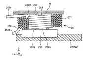
次に、可動部22を揺動させる駆動機構25について説明する。駆動機構25は、図6に示すように、永久磁石支持部222に設けられた永久磁石251と、永久磁石251と対向配置され、永久磁石251に作用させる磁界を発生させるコイル252と、を有する電磁アクチュエーターである。電磁アクチュエーターを用いることで、簡単な構成で、可動部22を揺動させるのに十分な力を発生させることができ、可動部22をスムーズに揺動させることができる。 Next, the
永久磁石251は、X軸方向に沿った長手形状をなしており、Z軸方向(ガラス板21の厚み方向)に磁化している。このような永久磁石251としては、特に限定されず、例えば、ネオジム磁石、フェライト磁石、サマリウムコバルト磁石、アルニコ磁石等を用いることができる。 The
一方、コイル252は、永久磁石251に対向配置されている。また、コイル252は、永久磁石251と離間して配置されている。コイル252と永久磁石251との離間距離(ギャップG)としては、特に限定されず、可動部22の大きさや、コイル252から発生する磁界の大きさ等によっても異なるが、例えば、0.1mm以上、0.5mm以下程度であることが好ましく、0.2mm以上、0.4mm以下程度であることがより好ましい。これにより、可動部22の揺動時における永久磁石251とコイル252の接触を防止しつつ、コイル252から発生する磁界をより効率的に永久磁石251に作用させることができる。そのため、可動部22をより効率的にかつ安定して揺動させることができる。 On the other hand, the
また、コイル252は、空芯コイルである。これにより、可動部22をよりスムーズに揺動させることができる。具体的に説明すると、例えば、コイル252として、内側に磁心を配置したものを用いた場合、生じる磁力の強さによっては、永久磁石251が磁心に引き付けられてしまい、これにより、揺動軸Jが変位し、可動部22の揺動をスムーズに行うことができなくなってしまう場合がある。このような不具合の発生を防止するためにもコイル252として空芯コイルを用いることが好ましい。 The
また、コイル252は、図7に示すように、永久磁石251の平面視形状に対応した略長方形となっている。そして、永久磁石251のコイル252と対向する側の面251aの輪郭は、面251aの平面視で、コイル252の永久磁石251と対向する側の面252cの内周の輪郭と外周の輪郭の間に位置している。すなわち、面251aの輪郭は、面252cの内周の輪郭よりも外側に位置し、外周の輪郭よりも内側に位置している。別の言い方をすると、長軸方向(X軸方向)における永久磁石251の幅をWx1とし、コイル252の内周の幅をWx2とし、コイル252の外周の幅をWx3としたとき、Wx2<Wx1<Wx3なる関係を満足し、短軸方向(Y軸方向)における永久磁石251の幅をWy1とし、コイル252の内周の幅をWy2とし、コイル252の外周の幅をWy3としたとき、Wy2<Wy1<Wy3なる関係を満足している。 Further, the
永久磁石251の輪郭とコイル252のサイズを上記のようにすることで、コイル252を小型化することができるため、コイル252に電流を印加した際の電力損失(発熱等)を抑えることができ、より効率的に省電力でコイル252から磁界を発生させることができる。また、コイル252から発生する磁界を、効率的に永久磁石251に作用させることができる。 By making the outline of the
このようなコイル252は、エナメル線、ホルマル線、ビニール線等の導体が絶縁体で覆われた導線253を巻回してなるものである。なお、導線253の直径としては、特に限定されないが、例えば、0.1mm以上、0.3mm以下程度とすることができる。また、コイル252では、コイル252の巻き始めの端部(引き出し位置)252aがコイル252の内周の+Z軸側端部に位置しており、巻き終わりの端部252bがコイル252の外周の−Z軸側端部に位置している。そして、端部252a、252bからは、巻回されていない状態(巻回方向と異なる方向に取回された状態)の導線253が引出配線253a、253bとして引き出されている。なお、コイル252の内周とは、空芯コイルの場合、導線253が巻回されることによって形成され通常磁心が配置される領域(空芯コイルなので磁心は存在しない)の輪郭を指し、コイル252が磁心を備える場合、磁心と導線253とが接触する位置(面251aの平面視で磁心の輪郭となる)で定義される。また、コイル252の外周とは、導線253が巻回されることによって形成される領域の外側の輪郭を指す。 Such a
以上のような駆動機構25では、図示しない電圧印加部からコイル252に駆動信号(交番電圧)を印加することでコイル252から磁界を発生させ、発生させた磁界を永久磁石251に作用させることで、可動部22を支持部23に対して揺動軸Jまわりに揺動(回動)させることができる。そして、このような可動部22の揺動によって、映像光LLの光軸がシフトされ、画像表示位置P1、P2に交互に画像が表示される。よって、見かけ上の画素が増加し、画像の高解像度化が図られる。 In the
コイル支持部26は、支持部23に支持(固定)されていると共に、コイル252を支持している。コイル支持部26の支持部23への支持方法としては特に限定されないが、例えば、ネジ止めによって支持することができる。このようなコイル支持部26は、図5(a)に示すように、コイル支持部26に対するコイル252の位置決めを行い易くするための位置決め用の貫通孔261と、コイル252の引出配線253aを通すための引出配線用の貫通孔262と、を有している。 The
位置決め用の貫通孔261は、X軸方向に離間して一対設けられている。そして、コイル252をコイル支持部26に対して適正な位置に配置した場合には、各貫通孔261とコイル252の内周とが重なるようになっている。言い換えると、コイル支持部26をコイル252が固定される固定面26aとは反対側の面から見たとき、コイル252をコイル支持部26に対して適正な位置に配置した場合には、各貫通孔261を介してコイル252の内周を視認することができる。このような位置決め用の貫通孔261を設けることで、コイル252をコイル支持部26に対して簡単に位置決めすることができる。 A pair of positioning through
また、位置決め用の貫通孔261は、さらに、可動部22を揺動させたときのダンパー効果を低減するための空気抜き用の貫通孔としても機能する。すなわち、可動部22が揺動してコイル支持部26に接近すると、これらの間の空気が圧縮され、この圧縮された空気が、可動部22のコイル支持部26側への揺動を阻害するおそれがある。そのため、貫通孔261を設け、この貫通孔261から可動部22とコイル支持部26との間の空気を逃がすことで、ダンパー効果を低減し、可動部22をよりスムーズに揺動させることができる。 Further, the positioning through-
一方、引出配線用の貫通孔262は、コイル252の一端側の引出配線253aを、コイル支持部26のコイル252が固定される固定面26a側から反対の面側へ、コイル252と固定面26aとの間を通さずに引き出すのに用いられる貫通孔である。このような貫通孔262は、図6に示すように、コイル支持部26の平面視(ガラス板21の厚さ方向から見た平面視)で、コイル252の内周と重なって、かつ、コイル252の巻き始めの端部(引き出し位置)252aと重なって配置されている。そして、この貫通孔262にコイル252の巻き始めの端部252aから延びる引出配線253aが挿通され、引出配線253aが固定面26aと反対の面側へ引き出されている。このような構成とすることで、次の効果を発揮することができる。 On the other hand, the through-
例えば、本実施形態とは異なり、図8に示すように、コイル252に巻回された導線253の内周(内周側)から引き出された引出配線253aをコイル支持部26とコイル252の間を通してコイル252の外側まで引き出した場合、引出配線253aの厚み(径)によってコイル252がコイル支持部26に対して傾いてしまうと共に、永久磁石251に対しても傾いてしまう。このようにコイル252が永久磁石251に対して傾いてしまうと、ある箇所では、コイル252と永久磁石251のギャップGが小さくなってしまい、コイル252と永久磁石251との接触が生じ、可動部22のスムーズな揺動が阻害されるおそれがある。反対に、このような接触を避けるためにコイル252と永久磁石251のギャップGを広げると、その分、コイル252から発生する磁界が永久磁石251に作用し難くなり(永久磁石251に作用する電磁力が低下し)、可動部22の駆動効率が低下する。 For example, unlike the present embodiment, as shown in FIG. 8, a
これに対して、本実施形態のように、引出配線253aを貫通孔262に挿通することで、上述した例とは異なり、引出配線253aをコイル支持部26とコイル252との間を通すことなく、コイル252の外側へ引き出すことができる。そのため、上述したようなコイル252の傾きが生じず、コイル252(コイル252の永久磁石251の面252c)と永久磁石251(永久磁石251のコイル252側の面251a)とを略平行に配置することができる(図6参照)。したがって、コイル252と永久磁石251との接触を防止しつつ、ギャップGを小さくすることができ、可動部22を効率的に駆動させることができる。 On the other hand, unlike the above-described example, the
特に、本実施形態では、貫通孔262がコイル支持部26の側面に開放する切り欠きで構成されている。そのため、コイル支持部26の側面に開放した開口を介して引出配線253aを貫通孔262内へ配置することができるため、引出配線253aの貫通孔262への挿通をより容易に行うことができる。ただし、貫通孔262の形状としては、引出配線253aを通すことができれば、本実施形態のような切り欠き状に限定されず、例えば、図9に示すように、コイル支持部26の側面に開放していなくてもよい。 In particular, in the present embodiment, the through
また、本実施形態では、貫通孔262に固定部材27が充填されており、固定部材27によって引出配線253aがコイル支持部26に固定されている。このように、引出配線253aをコイル支持部26に固定することで、引出配線253aの意図しない撓み等を抑制することができる。固定部材27としては、特に限定されないが、比較的軟質なものがよく、例えば、シリコーン系、エポキシ系、アクリル系等の各種樹脂接着剤を好適に用いることができる。なお、このような固定部材27は、省略してもよい。省略することで、前述した貫通孔262を貫通孔261と同様に、ダンパー効果を低減するための空気抜き用の貫通孔として機能させることができる。 In this embodiment, the fixing
また、前述したように、本実施形態では、永久磁石251のコイル252と対向する側の面251aの輪郭は、コイル252の永久磁石251と対向する側の面252cの外周の輪郭よりも内側に位置している。そのため、図6に示すように、Z軸方向から見た平面視で、永久磁石251の外側に、コイル252の外周に位置するコイル252の巻き終わりの端部252bが位置している。したがって、巻き終わりの端部252bから延びる引出配線253bを永久磁石251と接触することなく、コイル252の外側へ引き出すことができる。 Further, as described above, in the present embodiment, the contour of the
<第2実施形態>
図10は、本発明の第2実施形態に係る画像表示装置が有する光学デバイスを示す断面図である。Second Embodiment
FIG. 10 is a cross-sectional view showing an optical device included in the image display apparatus according to the second embodiment of the present invention.
以下、本発明の第2実施形態に係る画像表示装置について説明するが、前述した実施形態との相違点を中心に説明し、同様の事項はその説明を省略する。 Hereinafter, the image display apparatus according to the second embodiment of the present invention will be described. The description will focus on differences from the above-described embodiment, and description of similar matters will be omitted.
第2実施形態の画像表示装置は、光学デバイスの構成が異なること以外は、前述した第1実施形態と同様である。なお、前述した実施形態と同様の構成には、同一符号を付してある。 The image display apparatus of the second embodiment is the same as that of the first embodiment described above except that the configuration of the optical device is different. In addition, the same code | symbol is attached | subjected to the structure similar to embodiment mentioned above.
本実施形態の光学デバイス2が有するコイル支持部26では、図10に示すように、貫通孔262がコイル252の内周と重なることなく、コイル252の内周の内側に設けられている。このような構成によっても、コイル252の傾きが生じず、コイル252と永久磁石251との接触を防止しつつ、ギャップGを小さくすることができ、可動部22を効率的に駆動させることができる。 In the
このような第2実施形態によっても、前述した第1実施形態と同様の効果を発揮することができる。 Also according to the second embodiment, the same effects as those of the first embodiment described above can be exhibited.
<第3実施形態>
図11は、本発明の第3実施形態に係る画像表示装置が有する光学デバイスを示す断面図である。<Third Embodiment>
FIG. 11 is a cross-sectional view showing an optical device included in the image display apparatus according to the third embodiment of the present invention.
以下、本発明の第3実施形態に係る画像表示装置について説明するが、前述した実施形態との相違点を中心に説明し、同様の事項はその説明を省略する。 Hereinafter, the image display apparatus according to the third embodiment of the present invention will be described. The description will focus on differences from the above-described embodiment, and description of similar matters will be omitted.
第3実施形態の画像表示装置は、光学デバイスの構成が異なること以外は、前述した第1実施形態と同様である。なお、前述した実施形態と同様の構成には、同一符号を付してある。 The image display apparatus of the third embodiment is the same as that of the first embodiment described above except that the configuration of the optical device is different. In addition, the same code | symbol is attached | subjected to the structure similar to embodiment mentioned above.
本実施形態の光学デバイス2が有するコイル支持部26は、前述した第1実施形態の貫通孔262に替えて、図11に示すように、凹部263を有している。凹部263は、コイル252の引出配線253aをコイル支持部26とコイル252の間を通ってコイル252の外側まで引き出すのに用いられる凹部である。このような凹部263は、コイル支持部26の平面視で、コイル252の内周よりも内側から外周よりも外側まで延在し、また、端部252aと重なるように設けられている。また、凹部263の幅および深さは、それぞれ、導線253の径よりも大きくなっている。そして、図11に示すように、コイル252の内周から引き出された引出配線253aが、凹部263内を通ってコイル252の外側に引き出されている。 The
このような構成によれば、前述した第1実施形態で説明したようなコイル252の傾き(図8参照)が生じない。したがって、コイル252と永久磁石251との接触を防止しつつ、ギャップGを小さくすることができ、可動部22を効率的に駆動させることができる。 According to such a configuration, the inclination (see FIG. 8) of the
なお、本実施形態では、凹部263がコイル252の端部252aと重って設けられているが、凹部263は、コイルの端部252aと重なっていなくてもよい。また、本実施形態では、凹部263の一端部がコイル252の内周よりも内側まで延びているが、凹部263が端部252aと重なっており、凹部263に引出配線253aを挿入することができれば、例えば、凹部263は、コイル252の内周よりも内側まで延びていなくてもよい。 In the present embodiment, the
このような第3実施形態によっても、前述した第1実施形態と同様の効果を発揮することができる。 Also according to the third embodiment, the same effects as those of the first embodiment described above can be exhibited.
<第4実施形態>
図12は、本発明の第4実施形態に係る画像表示装置が有する光学デバイスを示す平面図である。<Fourth embodiment>
FIG. 12 is a plan view showing an optical device included in the image display apparatus according to the fourth embodiment of the present invention.
以下、本発明の第4実施形態に係る画像表示装置について説明するが、前述した実施形態との相違点を中心に説明し、同様の事項はその説明を省略する。 Hereinafter, an image display apparatus according to a fourth embodiment of the present invention will be described. The description will focus on differences from the above-described embodiment, and description of similar matters will be omitted.
第4実施形態の画像表示装置は、光学デバイスの構成が異なること以外は、前述した第1実施形態と同様である。なお、前述した実施形態と同様の構成には、同一符号を付してある。 The image display apparatus of the fourth embodiment is the same as that of the first embodiment described above except that the configuration of the optical device is different. In addition, the same code | symbol is attached | subjected to the structure similar to embodiment mentioned above.
本実施形態の光学デバイス2では、図12に示すように、駆動機構25が、揺動軸Jを介して一対設けられている。このように、駆動機構25を一対設けることで、可動部22をよりスムーズに揺動させることができる。 In the
このような第4実施形態によっても、前述した第1実施形態と同様の効果を発揮することができる。 According to the fourth embodiment, the same effect as that of the first embodiment described above can be exhibited.
<第5実施形態>
図13は、本発明の第5実施形態に係る画像表示装置の光学的な構成を示す図である。<Fifth Embodiment>
FIG. 13 is a diagram showing an optical configuration of an image display apparatus according to the fifth embodiment of the present invention.
以下、本発明の第5実施形態に係る画像表示装置について説明するが、前述した実施形態との相違点を中心に説明し、同様の事項はその説明を省略する。 Hereinafter, an image display apparatus according to a fifth embodiment of the present invention will be described. The description will focus on differences from the above-described embodiment, and description of similar matters will be omitted.
第5実施形態の画像表示装置は、半透過型(シースルー型)のヘッドマウントディスプレイ(以下、単に「HMD」とも言う)である。 The image display apparatus according to the fifth embodiment is a transflective (see-through) head mounted display (hereinafter also simply referred to as “HMD”).
本実施形態のHMD(画像表示装置)3は、観察者(使用者)に装着して使用されるものであり、図13に示すように、光源310と、液晶表示素子320と、投射レンズ系330と、導光部340と、光路偏向素子としての光学デバイス2と、を有している。光源310としては特に限定されないが、例えば、LEDのバックライトを用いることができる。このような光源310から発生する光は、液晶表示素子320に導かれる。液晶表示素子320は、透過型の液晶表示素子であり、例えば、HTPS(高温ポリシリコン)単板TFTカラー液晶パネル等を用いることができる。このような液晶表示素子320は、光源310からの光を変調して映像光を生成する。生成された映像光は、投射レンズ系で拡大された後、導光部340へ入射する。導光部340は、板状をなしており、さらに、光の伝搬方向の下流側にはハーフミラー341が配置される。導光部340内に導かれた光は、反射を繰り返して進み、ハーフミラー341によって観察者の瞳Eに導かれる。また、これと共に、外界光がハーフミラー341を透過して観察者の瞳Eに導かれる。したがって、HMD3では、景色に映像光が重畳して視認されることとなる。 The HMD (image display device) 3 of the present embodiment is used by being attached to an observer (user), and as shown in FIG. 13, a
このような構成のHMD3では、液晶表示素子320と投射レンズ系330との間に光学デバイス2が配置されており、これにより、映像光LLの光軸をシフトさせることができる。 In the HMD 3 having such a configuration, the
以上のような第5実施形態によっても、前述した第1実施形態と同様の効果を発揮することができる。 According to the fifth embodiment as described above, the same effect as that of the first embodiment described above can be exhibited.
<第6実施形態>
図14は、本発明の第6実施形態に係る画像表示装置の光学的な構成を示す図である。<Sixth Embodiment>
FIG. 14 is a diagram showing an optical configuration of an image display apparatus according to the sixth embodiment of the present invention.
以下、本発明の第6実施形態に係る画像表示装置について説明するが、前述した実施形態との相違点を中心に説明し、同様の事項はその説明を省略する。 Hereinafter, an image display apparatus according to a sixth embodiment of the present invention will be described. The description will focus on differences from the above-described embodiment, and description of similar matters will be omitted.
第6実施形態の画像表示装置は、ヘッドアップディスプレイ(以下、単に「HUD」とも言う)である。 The image display apparatus according to the sixth embodiment is a head-up display (hereinafter also simply referred to as “HUD”).
本実施形態のHUD(画像表示装置)5は、例えば、自動車に搭載され、フロントガラスFGを介して、時速、時間、走行距離等の各種情報(映像)を運転者に投影するのに用いられる。このようなHUD5は、図14に示すように、光源511、液晶表示素子512および投射レンズ系513を有する投影ユニット510と、反射ミラー520と、光路偏向素子としての光学デバイス2と、を有している。光源511、液晶表示素子512および投射レンズ系513は、例えば、前述した第3実施形態の光源310、液晶表示素子320および投射レンズ系330と同様の構成とすることができる。反射ミラー520は、凹面ミラーであり、投影ユニット510からの投影光を反射してフロントガラスFGに投影(表示)する。 The HUD (image display device) 5 of this embodiment is mounted on, for example, an automobile and is used to project various information (video) such as speed, time, and travel distance to a driver via a windshield FG. . As shown in FIG. 14, the HUD 5 has a
このような構成のHUD5では、液晶表示素子512と投射レンズ系513との間に光学デバイス2が配置されており、これにより、投影光の光軸をシフトさせることができる。 In the HUD 5 having such a configuration, the
以上のような第6実施形態によっても、前述した第1実施形態と同様の効果を発揮することができる。 According to the sixth embodiment as described above, the same effect as that of the first embodiment described above can be exhibited.
以上、本発明の光学デバイスおよび画像表示装置について、図示の実施形態に基づいて説明したが、本発明はこれに限定されるものではない。例えば、本発明の光学デバイスおよび画像表示装置では、各部の構成は、同様の機能を有する任意の構成のものに置換することができ、また、他の任意の構成を付加することもできる。 While the optical device and the image display apparatus of the present invention have been described based on the illustrated embodiments, the present invention is not limited to this. For example, in the optical device and the image display apparatus of the present invention, the configuration of each part can be replaced with an arbitrary configuration having a similar function, and other arbitrary configurations can be added.
また、前述した実施形態では、画像表示装置として、液晶プロジェクターおよび光走査型のプロジェクターについて説明したが、画像表示装置としては、プロジェクターに限定されず、その他、プリンター、スキャナー等にも適用可能である。 In the above-described embodiments, the liquid crystal projector and the optical scanning projector are described as the image display device. However, the image display device is not limited to the projector, and can be applied to a printer, a scanner, and the like. .
1……プロジェクター
102……光源
104a、104b、104c……ミラー
106a、106b……ダイクロイックミラー
108B、108G、108R……液晶表示素子
110……ダイクロイックプリズム
112……投射レンズ系
120……制御回路
122……画像信号処理回路
2……光学デバイス
21……ガラス板
22……可動部
221……ガラス板支持部
221a……貫通孔
221b……爪部
222……永久磁石支持部
222a……凹部
23……支持部
24a、24b……軸部
25……駆動機構
251……永久磁石
251a……面
252……コイル
252a、252b……端部
252c……面
253……導線
253a、253b……引出配線
26……コイル支持部
26a……固定面
261……貫通孔
262……貫通孔
263……凹部
27……固定部材
3……HMD
310……光源
320……液晶表示素子
330……投射レンズ系
340……導光部
341……ハーフミラー
5……HUD
510……投影ユニット
511……光源
512……液晶表示素子
513……投射レンズ系
520……反射ミラー
8……スクリーン
E……瞳
FG……フロントガラス
G……ギャップ
J……揺動軸
LL……映像光
P1、P2……画像表示位置
Px……画素
Bv、Gv、Rv……データ信号
Vid……画像信号DESCRIPTION OF SYMBOLS 1 ...
310 ……
510 ……
Claims (10)
Translated fromJapanese前記光学部を支持する可動部と、
前記可動部を揺動軸まわりに揺動可能に支持する軸部と、
前記軸部を支持する支持部と、
前記可動部に設けられた永久磁石と、
前記永久磁石に作用させる磁界を発生させるコイルと、
前記支持部に支持され、前記コイルを支持するコイル支持部と、を有し、
前記コイルは、導線を巻回して構成され、
前記導線の一端は、前記コイルに巻回された前記導線の内周から引き出され、
前記コイル支持部は、前記光学部の厚さ方向からの平面視で、前記コイルの内周と重なるように形成された貫通孔を有し、
前記コイルの内周側から引き出された前記導線は、前記貫通孔に挿通されていることを特徴とする光学デバイス。An optical unit having a light incident surface on which light is incident;
A movable part that supports the optical part;
A shaft portion that supports the movable portion so as to be swingable about a swing shaft;
A support portion for supporting the shaft portion;
A permanent magnet provided on the movable part;
A coil that generates a magnetic field that acts on the permanent magnet;
A coil support that is supported by the support and supports the coil;
The coil is configured by winding a conductive wire,
One end of the conducting wire is drawn out from the inner circumference of the conducting wire wound around the coil,
The coil support part has a through-hole formed so as to overlap with the inner periphery of the coil in a plan view from the thickness direction of the optical part,
The optical device, wherein the conducting wire drawn from the inner peripheral side of the coil is inserted into the through hole.
前記光学部を支持する可動部と、
前記可動部を揺動軸まわりに揺動可能に支持する軸部と、
前記軸部を支持する支持部と、
前記可動部に設けられた永久磁石と、
前記永久磁石に作用させる磁界を発生させるコイルと、
前記支持部に支持され、前記コイルを支持するコイル支持部と、を有し、
前記コイルは、導線を巻回して構成され、
前記導線の一端は、前記コイルに巻回された前記導線の内周から引き出され、
前記コイル支持部は、前記光学部の厚さ方向からの平面視で、前記コイルの内周の内側に位置する貫通孔を有し、
前記コイルに巻回された前記導線の内周から引き出された前記導線は、前記貫通孔に挿通されていることを特徴とする光学デバイス。An optical unit having a light incident surface on which light is incident;
A movable part that supports the optical part;
A shaft portion that supports the movable portion so as to be swingable about a swing shaft;
A support portion for supporting the shaft portion;
A permanent magnet provided on the movable part;
A coil that generates a magnetic field that acts on the permanent magnet;
A coil support that is supported by the support and supports the coil;
The coil is configured by winding a conductive wire,
One end of the conducting wire is drawn out from the inner circumference of the conducting wire wound around the coil,
The coil support part has a through hole located inside the inner periphery of the coil in a plan view from the thickness direction of the optical part,
The optical device, wherein the conducting wire drawn from the inner periphery of the conducting wire wound around the coil is inserted into the through hole.
前記光学部を支持する可動部と、
前記可動部を揺動軸まわりに揺動可能に支持する軸部と、
前記軸部を支持する支持部と、
前記可動部に設けられた永久磁石と、
前記永久磁石に作用させる磁界を発生させるコイルと、
前記支持部に支持され、前記コイルを支持するコイル支持部と、を有し、
前記コイルは、導線を巻回して構成され、
前記導線の一端は、前記コイルに巻回された前記導線の内周から引き出され、
前記コイル支持部は、前記光学部の厚さ方向からの平面視で、前記コイルの内周よりも内側から外周よりも外側まで延在して形成された凹部を有し、
前記コイルに巻回された前記導線の内周から引き出された前記導線は、前記凹部を通って前記コイルの外側に引き出されていることを特徴とする光学デバイス。An optical unit having a light incident surface on which light is incident;
A movable part that supports the optical part;
A shaft portion that supports the movable portion so as to be swingable about a swing shaft;
A support portion for supporting the shaft portion;
A permanent magnet provided on the movable part;
A coil that generates a magnetic field that acts on the permanent magnet;
A coil support that is supported by the support and supports the coil;
The coil is configured by winding a conductive wire,
One end of the conducting wire is drawn out from the inner circumference of the conducting wire wound around the coil,
The coil support portion has a recess formed by extending from the inner side to the outer side of the outer periphery than the inner periphery of the coil in a plan view from the thickness direction of the optical unit,
The optical device, wherein the conducting wire drawn from the inner periphery of the conducting wire wound around the coil is drawn to the outside of the coil through the recess.
前記コイルと前記永久磁石とは対向配置され、
前記永久磁石の前記コイルと対向する側の面の輪郭は、前記面の平面視で、前記コイルの前記永久磁石と対向する側の面の内周の輪郭よりも外側に位置している請求項1ないし5のいずれか1項に記載の光学デバイス。The coil is an air-core coil;
The coil and the permanent magnet are arranged to face each other,
The contour of the surface of the permanent magnet facing the coil is located outside the contour of the inner periphery of the surface of the coil facing the permanent magnet in a plan view of the surface. The optical device according to any one of 1 to 5.
前記コイルと前記永久磁石とは対向配置され、
前記永久磁石の前記コイルと対向する側の面の輪郭は、前記面の平面視で、前記コイルの前記永久磁石と対向する側の面の外周の輪郭よりも内側に位置している請求項1ないし6のいずれか1項に記載の光学デバイス。The coil is an air-core coil;
The coil and the permanent magnet are arranged to face each other,
The contour of the surface of the permanent magnet facing the coil is located inside the contour of the outer periphery of the surface of the coil facing the permanent magnet in a plan view of the surface. 7. The optical device according to any one of items 6 to 6.
前記光学デバイスで光を空間変調させることにより、前記光の照射によって表示される画素の位置をずらすように構成されている請求項9に記載の画像表示装置。The optical unit transmits the light,
The image display apparatus according to claim 9, wherein a position of a pixel displayed by the light irradiation is shifted by spatially modulating light with the optical device.
Priority Applications (3)
| Application Number | Priority Date | Filing Date | Title |
|---|---|---|---|
| JP2015116897AJP2017003744A (en) | 2015-06-09 | 2015-06-09 | Optical device and image display device |
| CN201610349986.2ACN106249401A (en) | 2015-06-09 | 2016-05-24 | Optics and image display device |
| US15/163,829US9823553B2 (en) | 2015-06-09 | 2016-05-25 | Optical device and image display apparatus |
Applications Claiming Priority (1)
| Application Number | Priority Date | Filing Date | Title |
|---|---|---|---|
| JP2015116897AJP2017003744A (en) | 2015-06-09 | 2015-06-09 | Optical device and image display device |
Publications (1)
| Publication Number | Publication Date |
|---|---|
| JP2017003744Atrue JP2017003744A (en) | 2017-01-05 |
Family
ID=57516674
Family Applications (1)
| Application Number | Title | Priority Date | Filing Date |
|---|---|---|---|
| JP2015116897APendingJP2017003744A (en) | 2015-06-09 | 2015-06-09 | Optical device and image display device |
Country Status (3)
| Country | Link |
|---|---|
| US (1) | US9823553B2 (en) |
| JP (1) | JP2017003744A (en) |
| CN (1) | CN106249401A (en) |
Cited By (2)
| Publication number | Priority date | Publication date | Assignee | Title |
|---|---|---|---|---|
| WO2022153602A1 (en)* | 2021-01-14 | 2022-07-21 | 株式会社村田製作所 | Linear vibration motor and electronic device |
| US11683457B2 (en) | 2020-10-23 | 2023-06-20 | Seiko Epson Corportation | Optical device and image display device |
Families Citing this family (27)
| Publication number | Priority date | Publication date | Assignee | Title |
|---|---|---|---|---|
| GB0718706D0 (en) | 2007-09-25 | 2007-11-07 | Creative Physics Ltd | Method and apparatus for reducing laser speckle |
| US11726332B2 (en) | 2009-04-27 | 2023-08-15 | Digilens Inc. | Diffractive projection apparatus |
| WO2016020630A2 (en) | 2014-08-08 | 2016-02-11 | Milan Momcilo Popovich | Waveguide laser illuminator incorporating a despeckler |
| US9933684B2 (en) | 2012-11-16 | 2018-04-03 | Rockwell Collins, Inc. | Transparent waveguide display providing upper and lower fields of view having a specific light output aperture configuration |
| WO2016113534A1 (en) | 2015-01-12 | 2016-07-21 | Milan Momcilo Popovich | Environmentally isolated waveguide display |
| US9632226B2 (en) | 2015-02-12 | 2017-04-25 | Digilens Inc. | Waveguide grating device |
| CN113759555B (en) | 2015-10-05 | 2024-09-20 | 迪吉伦斯公司 | Waveguide Display |
| WO2018102834A2 (en) | 2016-12-02 | 2018-06-07 | Digilens, Inc. | Waveguide device with uniform output illumination |
| US10545346B2 (en) | 2017-01-05 | 2020-01-28 | Digilens Inc. | Wearable heads up displays |
| WO2019079350A2 (en)* | 2017-10-16 | 2019-04-25 | Digilens, Inc. | Systems and methods for multiplying the image resolution of a pixelated display |
| EP3710894B1 (en) | 2018-01-08 | 2025-07-30 | Digilens Inc. | Methods for fabricating optical waveguides |
| US10732569B2 (en) | 2018-01-08 | 2020-08-04 | Digilens Inc. | Systems and methods for high-throughput recording of holographic gratings in waveguide cells |
| CN108259882B (en)* | 2018-04-08 | 2019-12-10 | 京东方科技集团股份有限公司 | A display device and display method thereof |
| US11126069B2 (en)* | 2018-06-27 | 2021-09-21 | Coretronic Corporation | Projector and optical module including extending wire |
| US20200225471A1 (en) | 2019-01-14 | 2020-07-16 | Digilens Inc. | Holographic Waveguide Display with Light Control Layer |
| US20200247017A1 (en) | 2019-02-05 | 2020-08-06 | Digilens Inc. | Methods for Compensating for Optical Surface Nonuniformity |
| KR102866596B1 (en) | 2019-02-15 | 2025-09-29 | 디지렌즈 인코포레이티드. | Method and device for providing a holographic waveguide display using an integral grating |
| US20220283377A1 (en) | 2019-02-15 | 2022-09-08 | Digilens Inc. | Wide Angle Waveguide Display |
| CN210075447U (en)* | 2019-04-30 | 2020-02-14 | 中强光电股份有限公司 | Opto-mechanical module and projection device |
| JP2020190672A (en)* | 2019-05-23 | 2020-11-26 | セイコーエプソン株式会社 | Optical device, control method for optical device, and image display unit |
| EP3980825A4 (en) | 2019-06-07 | 2023-05-03 | Digilens Inc. | WAVEGUIDES WITH TRANSMITTING AND REFLECTING GRIDS AND RELATED MANUFACTURING PROCESSES |
| EP4004646A4 (en) | 2019-07-29 | 2023-09-06 | Digilens Inc. | METHODS AND APPARATUS FOR MULTIPLYING THE IMAGE RESOLUTION AND FIELD OF VIEW OF A PIXELATED DISPLAY SCREEN |
| KR102775783B1 (en) | 2019-08-29 | 2025-02-28 | 디지렌즈 인코포레이티드. | Vacuum grid and method for manufacturing the same |
| JP7307031B2 (en)* | 2020-05-29 | 2023-07-11 | 株式会社日立エルジーデータストレージ | Virtual image projection device |
| JP7543872B2 (en)* | 2020-11-20 | 2024-09-03 | セイコーエプソン株式会社 | Optical device driving method, optical system, and display device |
| WO2022150841A1 (en) | 2021-01-07 | 2022-07-14 | Digilens Inc. | Grating structures for color waveguides |
| US12158612B2 (en) | 2021-03-05 | 2024-12-03 | Digilens Inc. | Evacuated periodic structures and methods of manufacturing |
Citations (16)
| Publication number | Priority date | Publication date | Assignee | Title |
|---|---|---|---|---|
| JPS5886851A (en)* | 1981-11-14 | 1983-05-24 | Hitachi Ltd | Armature coil for plane opposite type motor |
| JPH0682711A (en)* | 1992-08-31 | 1994-03-25 | Matsushita Electric Works Ltd | Driving device of scanning mirror |
| JPH0727989A (en)* | 1993-07-07 | 1995-01-31 | Fuji Electric Co Ltd | Light deflector |
| JPH07113998A (en)* | 1993-10-15 | 1995-05-02 | Sony Corp | Projection display device |
| JPH09191626A (en)* | 1996-01-10 | 1997-07-22 | Oputoron:Kk | Resonance type scanner |
| JPH09322503A (en)* | 1996-05-30 | 1997-12-12 | Sankyo Seiki Mfg Co Ltd | Compact motor |
| JP2000324789A (en)* | 1999-05-14 | 2000-11-24 | Sansen:Kk | Drive coil for linear motor and method of manufacturing the same |
| US20050264501A1 (en)* | 2004-06-01 | 2005-12-01 | Lg Electronics Inc. | Display device |
| JP2005338241A (en)* | 2004-05-25 | 2005-12-08 | Canon Inc | Oscillator, image forming apparatus using the same, and speckle reduction method |
| JP2006230103A (en)* | 2005-02-17 | 2006-08-31 | Shinano Kenshi Co Ltd | Electromagnetic drive actuator and electromagnetic pump |
| JP2008304667A (en)* | 2007-06-07 | 2008-12-18 | Seiko Epson Corp | Actuator, optical scanner and image forming apparatus |
| JP2010230730A (en)* | 2009-03-25 | 2010-10-14 | Seiko Epson Corp | Image forming apparatus |
| WO2011074256A1 (en)* | 2009-12-16 | 2011-06-23 | キヤノン電子株式会社 | Vibration element, optical scanning device, actuator, image projecting device, and image forming device |
| JP2011158589A (en)* | 2010-01-29 | 2011-08-18 | Mitsubishi Electric Corp | Optical path controller and projection image display apparatus |
| JP2013038835A (en)* | 2011-08-03 | 2013-02-21 | Nippon Densan Corp | Method of manufacturing spindle motor, spindle motor, and disk drive |
| JP2014036447A (en)* | 2012-08-07 | 2014-02-24 | Nippon Densan Corp | Spindle motor, and disk drive |
Family Cites Families (12)
| Publication number | Priority date | Publication date | Assignee | Title |
|---|---|---|---|---|
| KR20050118510A (en) | 2004-06-14 | 2005-12-19 | 엘지전자 주식회사 | Apparatus for improving resolution of display apparatus and method thereof |
| US7665853B2 (en)* | 2006-06-05 | 2010-02-23 | Symbol Technologies, Inc. | Arrangement for, and method of, enhancing image projection by holding scan mirror steady during part of mirror drive cycle |
| WO2010021215A1 (en)* | 2008-08-18 | 2010-02-25 | コニカミノルタオプト株式会社 | Image projection device |
| JP2011090155A (en) | 2009-10-22 | 2011-05-06 | Seiko Epson Corp | Control device and electronic equipment |
| JP5569084B2 (en) | 2010-03-25 | 2014-08-13 | セイコーエプソン株式会社 | Image display device and image display method |
| JP5659642B2 (en) | 2010-09-10 | 2015-01-28 | セイコーエプソン株式会社 | Optical scanner, optical scanner manufacturing method, and image forming apparatus |
| JP5990948B2 (en) | 2011-06-22 | 2016-09-14 | セイコーエプソン株式会社 | projector |
| JP5872073B2 (en)* | 2012-12-21 | 2016-03-01 | 三菱電機株式会社 | Optical scanning device and projector |
| US9223129B2 (en)* | 2013-04-19 | 2015-12-29 | Microvision, Inc. | MEMS device with multi-segment flexures |
| JP2016126103A (en) | 2014-12-26 | 2016-07-11 | セイコーエプソン株式会社 | Optical device, image display device, and method for manufacturing optical device |
| JP6398754B2 (en) | 2015-01-30 | 2018-10-03 | セイコーエプソン株式会社 | Optical device and image display apparatus |
| JP6492701B2 (en) | 2015-01-30 | 2019-04-03 | セイコーエプソン株式会社 | Image display device |
- 2015
- 2015-06-09JPJP2015116897Apatent/JP2017003744A/enactivePending
- 2016
- 2016-05-24CNCN201610349986.2Apatent/CN106249401A/enactivePending
- 2016-05-25USUS15/163,829patent/US9823553B2/enactiveActive
Patent Citations (16)
| Publication number | Priority date | Publication date | Assignee | Title |
|---|---|---|---|---|
| JPS5886851A (en)* | 1981-11-14 | 1983-05-24 | Hitachi Ltd | Armature coil for plane opposite type motor |
| JPH0682711A (en)* | 1992-08-31 | 1994-03-25 | Matsushita Electric Works Ltd | Driving device of scanning mirror |
| JPH0727989A (en)* | 1993-07-07 | 1995-01-31 | Fuji Electric Co Ltd | Light deflector |
| JPH07113998A (en)* | 1993-10-15 | 1995-05-02 | Sony Corp | Projection display device |
| JPH09191626A (en)* | 1996-01-10 | 1997-07-22 | Oputoron:Kk | Resonance type scanner |
| JPH09322503A (en)* | 1996-05-30 | 1997-12-12 | Sankyo Seiki Mfg Co Ltd | Compact motor |
| JP2000324789A (en)* | 1999-05-14 | 2000-11-24 | Sansen:Kk | Drive coil for linear motor and method of manufacturing the same |
| JP2005338241A (en)* | 2004-05-25 | 2005-12-08 | Canon Inc | Oscillator, image forming apparatus using the same, and speckle reduction method |
| US20050264501A1 (en)* | 2004-06-01 | 2005-12-01 | Lg Electronics Inc. | Display device |
| JP2006230103A (en)* | 2005-02-17 | 2006-08-31 | Shinano Kenshi Co Ltd | Electromagnetic drive actuator and electromagnetic pump |
| JP2008304667A (en)* | 2007-06-07 | 2008-12-18 | Seiko Epson Corp | Actuator, optical scanner and image forming apparatus |
| JP2010230730A (en)* | 2009-03-25 | 2010-10-14 | Seiko Epson Corp | Image forming apparatus |
| WO2011074256A1 (en)* | 2009-12-16 | 2011-06-23 | キヤノン電子株式会社 | Vibration element, optical scanning device, actuator, image projecting device, and image forming device |
| JP2011158589A (en)* | 2010-01-29 | 2011-08-18 | Mitsubishi Electric Corp | Optical path controller and projection image display apparatus |
| JP2013038835A (en)* | 2011-08-03 | 2013-02-21 | Nippon Densan Corp | Method of manufacturing spindle motor, spindle motor, and disk drive |
| JP2014036447A (en)* | 2012-08-07 | 2014-02-24 | Nippon Densan Corp | Spindle motor, and disk drive |
Cited By (2)
| Publication number | Priority date | Publication date | Assignee | Title |
|---|---|---|---|---|
| US11683457B2 (en) | 2020-10-23 | 2023-06-20 | Seiko Epson Corportation | Optical device and image display device |
| WO2022153602A1 (en)* | 2021-01-14 | 2022-07-21 | 株式会社村田製作所 | Linear vibration motor and electronic device |
Also Published As
| Publication number | Publication date |
|---|---|
| US9823553B2 (en) | 2017-11-21 |
| US20160363840A1 (en) | 2016-12-15 |
| CN106249401A (en) | 2016-12-21 |
Similar Documents
| Publication | Publication Date | Title |
|---|---|---|
| JP2017003744A (en) | Optical device and image display device | |
| JP6398754B2 (en) | Optical device and image display apparatus | |
| US9519134B2 (en) | Optical device and image display apparatus | |
| JP6784125B2 (en) | Optical device unit and image display device | |
| JP6451187B2 (en) | Optical device and image display apparatus | |
| JP6569329B2 (en) | Optical device and image display apparatus | |
| US9799249B2 (en) | Optical device and image display apparatus | |
| JP2020091343A (en) | Optical path shift device and image display device | |
| US9651773B2 (en) | Optical device, image display device, and method of manufacturing optical device | |
| JP6507550B2 (en) | Optical device, image display device and projector | |
| US9602790B2 (en) | Optical device and image display apparatus | |
| JP6455080B2 (en) | Optical device and image display apparatus | |
| CN106842554B (en) | Optical device and image display apparatus | |
| CN105467580B (en) | Optical device and image display device |
Legal Events
| Date | Code | Title | Description |
|---|---|---|---|
| A621 | Written request for application examination | Free format text:JAPANESE INTERMEDIATE CODE: A621 Effective date:20180515 | |
| A977 | Report on retrieval | Free format text:JAPANESE INTERMEDIATE CODE: A971007 Effective date:20190212 | |
| A131 | Notification of reasons for refusal | Free format text:JAPANESE INTERMEDIATE CODE: A131 Effective date:20190305 | |
| A521 | Request for written amendment filed | Free format text:JAPANESE INTERMEDIATE CODE: A523 Effective date:20190418 | |
| A131 | Notification of reasons for refusal | Free format text:JAPANESE INTERMEDIATE CODE: A131 Effective date:20190910 | |
| A521 | Request for written amendment filed | Free format text:JAPANESE INTERMEDIATE CODE: A523 Effective date:20191108 | |
| A02 | Decision of refusal | Free format text:JAPANESE INTERMEDIATE CODE: A02 Effective date:20200303 |