JP2016527482A - Method for driving a time-of-flight system - Google Patents
Method for driving a time-of-flight systemDownload PDFInfo
- Publication number
- JP2016527482A JP2016527482AJP2016518541AJP2016518541AJP2016527482AJP 2016527482 AJP2016527482 AJP 2016527482AJP 2016518541 AJP2016518541 AJP 2016518541AJP 2016518541 AJP2016518541 AJP 2016518541AJP 2016527482 AJP2016527482 AJP 2016527482A
- Authority
- JP
- Japan
- Prior art keywords
- signal
- tap
- taps
- pixel
- time
- Prior art date
- Legal status (The legal status is an assumption and is not a legal conclusion. Google has not performed a legal analysis and makes no representation as to the accuracy of the status listed.)
- Granted
Links
Images


Classifications
- G—PHYSICS
- G01—MEASURING; TESTING
- G01S—RADIO DIRECTION-FINDING; RADIO NAVIGATION; DETERMINING DISTANCE OR VELOCITY BY USE OF RADIO WAVES; LOCATING OR PRESENCE-DETECTING BY USE OF THE REFLECTION OR RERADIATION OF RADIO WAVES; ANALOGOUS ARRANGEMENTS USING OTHER WAVES
- G01S7/00—Details of systems according to groups G01S13/00, G01S15/00, G01S17/00
- G01S7/48—Details of systems according to groups G01S13/00, G01S15/00, G01S17/00 of systems according to group G01S17/00
- G01S7/491—Details of non-pulse systems
- G01S7/4912—Receivers
- G01S7/4913—Circuits for detection, sampling, integration or read-out
- G01S7/4914—Circuits for detection, sampling, integration or read-out of detector arrays, e.g. charge-transfer gates
- G—PHYSICS
- G01—MEASURING; TESTING
- G01S—RADIO DIRECTION-FINDING; RADIO NAVIGATION; DETERMINING DISTANCE OR VELOCITY BY USE OF RADIO WAVES; LOCATING OR PRESENCE-DETECTING BY USE OF THE REFLECTION OR RERADIATION OF RADIO WAVES; ANALOGOUS ARRANGEMENTS USING OTHER WAVES
- G01S17/00—Systems using the reflection or reradiation of electromagnetic waves other than radio waves, e.g. lidar systems
- G01S17/02—Systems using the reflection of electromagnetic waves other than radio waves
- G01S17/06—Systems determining position data of a target
- G01S17/08—Systems determining position data of a target for measuring distance only
- G01S17/32—Systems determining position data of a target for measuring distance only using transmission of continuous waves, whether amplitude-, frequency-, or phase-modulated, or unmodulated
- G01S17/36—Systems determining position data of a target for measuring distance only using transmission of continuous waves, whether amplitude-, frequency-, or phase-modulated, or unmodulated with phase comparison between the received signal and the contemporaneously transmitted signal
- G—PHYSICS
- G01—MEASURING; TESTING
- G01S—RADIO DIRECTION-FINDING; RADIO NAVIGATION; DETERMINING DISTANCE OR VELOCITY BY USE OF RADIO WAVES; LOCATING OR PRESENCE-DETECTING BY USE OF THE REFLECTION OR RERADIATION OF RADIO WAVES; ANALOGOUS ARRANGEMENTS USING OTHER WAVES
- G01S17/00—Systems using the reflection or reradiation of electromagnetic waves other than radio waves, e.g. lidar systems
- G01S17/88—Lidar systems specially adapted for specific applications
- G01S17/89—Lidar systems specially adapted for specific applications for mapping or imaging
- G01S17/894—3D imaging with simultaneous measurement of time-of-flight at a 2D array of receiver pixels, e.g. time-of-flight cameras or flash lidar
- H—ELECTRICITY
- H10—SEMICONDUCTOR DEVICES; ELECTRIC SOLID-STATE DEVICES NOT OTHERWISE PROVIDED FOR
- H10F—INORGANIC SEMICONDUCTOR DEVICES SENSITIVE TO INFRARED RADIATION, LIGHT, ELECTROMAGNETIC RADIATION OF SHORTER WAVELENGTH OR CORPUSCULAR RADIATION
- H10F39/00—Integrated devices, or assemblies of multiple devices, comprising at least one element covered by group H10F30/00, e.g. radiation detectors comprising photodiode arrays
- H10F39/10—Integrated devices
- H10F39/12—Image sensors
- H10F39/18—Complementary metal-oxide-semiconductor [CMOS] image sensors; Photodiode array image sensors
- H—ELECTRICITY
- H10—SEMICONDUCTOR DEVICES; ELECTRIC SOLID-STATE DEVICES NOT OTHERWISE PROVIDED FOR
- H10F—INORGANIC SEMICONDUCTOR DEVICES SENSITIVE TO INFRARED RADIATION, LIGHT, ELECTROMAGNETIC RADIATION OF SHORTER WAVELENGTH OR CORPUSCULAR RADIATION
- H10F39/00—Integrated devices, or assemblies of multiple devices, comprising at least one element covered by group H10F30/00, e.g. radiation detectors comprising photodiode arrays
- H10F39/80—Constructional details of image sensors
- H10F39/802—Geometry or disposition of elements in pixels, e.g. address-lines or gate electrodes
- H—ELECTRICITY
- H10—SEMICONDUCTOR DEVICES; ELECTRIC SOLID-STATE DEVICES NOT OTHERWISE PROVIDED FOR
- H10F—INORGANIC SEMICONDUCTOR DEVICES SENSITIVE TO INFRARED RADIATION, LIGHT, ELECTROMAGNETIC RADIATION OF SHORTER WAVELENGTH OR CORPUSCULAR RADIATION
- H10F39/00—Integrated devices, or assemblies of multiple devices, comprising at least one element covered by group H10F30/00, e.g. radiation detectors comprising photodiode arrays
- H10F39/80—Constructional details of image sensors
- H10F39/803—Pixels having integrated switching, control, storage or amplification elements
Landscapes
- Physics & Mathematics (AREA)
- Engineering & Computer Science (AREA)
- Electromagnetism (AREA)
- Computer Networks & Wireless Communication (AREA)
- General Physics & Mathematics (AREA)
- Radar, Positioning & Navigation (AREA)
- Remote Sensing (AREA)
- Optical Radar Systems And Details Thereof (AREA)
Abstract
Translated fromJapaneseDescription
Translated fromJapanese本発明は飛行時間システムに関し、さらに詳しくは、飛行時間システムを駆動するための方法に関する。 The present invention relates to a time-of-flight system, and more particularly to a method for driving a time-of-flight system.
コンピュータビジョンは、画像を取得し、処理し、解析し、かつ理解するための方法を含む成長中の研究分野である。この分野における主な推進的思想は、シーンの画像を電子的に知覚しかつ理解することによって、人間の視覚の能力を複製することである。特に、コンピュータビジョンの研究の1つの主題は、奥行感覚あるいは換言すると立体(3D)視である。 Computer vision is a growing field of research that includes methods for acquiring, processing, analyzing, and understanding images. The main driving idea in this field is to replicate human visual ability by electronically perceiving and understanding scene images. In particular, one subject of computer vision research is depth sensation or, in other words, stereoscopic (3D) vision.
カメラおよびデータ処理手段を含む飛行時間(ToF)システムは最近登場したものであり、光源から物体への光の飛行時間を解析することによって、シーン(環境、領域、scene)の3D画像を取得することができる。そのようなカメラシステムは、定点からの奥行または距離情報が要求される多くの用途で使用される。 Time-of-flight (ToF) systems, including cameras and data processing means, have recently emerged and acquire 3D images of scenes (environments, regions, scenes) by analyzing the time of flight of light from a light source to an object. be able to. Such camera systems are used in many applications where depth or distance information from a fixed point is required.
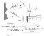
図1に示すToFシステム3の基本的動作原理は、パルスのような変調光16によりシーン15を照明することである。変調光16はシーン15内の物体から反射して戻り、レンズは反射した光17を集め、シーンにおける物体の像を撮像センサ35上に、特にセンサのセンサ面上に形成する。カメラからの物体の距離に応じて、変調光、例えばパルスの出射と、カメラにおけるそれらの反射の受光との間に遅延が経験される。例えば、カメラから2.5m離れた物体は16.66nsの時間遅延を生じさせる。この遅延を解析することによって、特に相関計算を実施することによって、前記物体のカメラからの距離を引き出すことができる。 The basic operating principle of the ToF system 3 shown in FIG. 1 is to illuminate the
物体のカメラからの距離を次のように算出することができる。分かり易くするために、信号の例を図2に掲げる。変調信号16(S)は物体に向けて送られる。物体で反射した後、信号17(Sφ)は光検出器によって検出される。この信号Sφは、伝搬時間のため、原信号Sと比較して位相φだけ位相シフトされる。The distance of the object from the camera can be calculated as follows. For the sake of clarity, examples of signals are given in FIG. The modulation signal 16 (S) is sent toward the object. After reflection at the object, the signal 17 (Sφ ) is detected by a photodetector. This signalSφ is phase-shifted by a phase φ compared to the original signal S due to propagation time.
φは、カメラからの物体の距離を測定するための主要パラメータである。このパラメータを測定するために、光検出信号Sφは通常、SI、
および
および
φの抽出は変調信号Sの波形に依存する。例えばSが正弦波である場合、次のようになる。
and
and
The extraction of φ depends on the waveform of the modulation signal S. For example, when S is a sine wave, it is as follows.
方程式1〜4から、理論的に、それぞれSφ,I、
実際には、ToFの測定は一般的に、ToF画素のアレイを含むToFセンサによって実行される。先行技術では、これらの画素の各々は一般的に1つまたは2つの「タップ」を含む。「タップ」は、Sφのような光信号にさらされたときに電荷を光生成するために使用される制御ノードおよび検出領域を含む構成要素である。画素当たり1つまたは2つのタップしか持たないということは、実際にはSφの測度が時系列であることを含む。例えば、1つのタップだけを含む画素は、I、Q、および次いでDφを算出するために、4つの異なる信号Sφ1‐4を連続的に測定しなければならない。これらの構成では、数回の露光が発生し、各露光の間に物体が移動すると、奥行データDφは破損される。In practice, the measurement of ToF is typically performed by a ToF sensor that includes an array of ToF pixels. In the prior art, each of these pixels typically includes one or two “taps”. A “tap” is a component that includes a control node and a detection region that are used to photogenerate charge when exposed to an optical signal such asSφ . Having only one or two taps per pixel actuallymeans that the measure of Sφ is time series. For example, a pixel containing only one tap must continuously measure four different signals Sφ1-4 to calculate I, Q, and then Dφ . In these configurations, when the exposure occurs several times and the object moves during each exposure, the depth dataDφ is corrupted.
画素当たり1つまたは2つのタップしか使用しないことは、奥行計算の一貫性の点で問題であるが、それだけではない。それは設計上の理由からも問題である。実際、幾つかの異なる信号Sφiが測定される場合、計算ステップの前に信号Sφiを保存するために、センサレベルまたはシステムレベルで画素にメモリを追加しなければならない。そうするとToFシステムのサイズは劇的に増大する。Using only one or two taps per pixel is a problem in the depth calculation consistency, but it is not the only one. That is also a problem for design reasons. In fact, if several different signalsSφi are measured, a memory must be added to the pixel at the sensor level or system level in order to store the signalSφi before the calculation step. This dramatically increases the size of the ToF system.
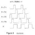
最終的に、幾つかのタップが単一の画素に含まれる場合、それらを駆動するために使用される駆動信号は、要求される帯域幅が高すぎるため、往々にして最適ではない。他のタップに対して正電位がタップに印加されると、そのタップは起動され、検出能が高くなる。すなわち、起動されたタップの検出領域は、画素における光生成された少数キャリアの大部分を受け取る。4タップ画素のアーキテクチャでは、単刀直入な手法は、図3に示すように、4つのタップの各々を変調周期の25%ずつ使用可能にすることである。周波数が50MHzの送信変調信号の場合、4タップデバイスのタップは、各タップの25%のデューティサイクルのため、100MHzと同等の応答時間を必要とする。 Finally, if several taps are included in a single pixel, the drive signal used to drive them is often not optimal because the required bandwidth is too high. When a positive potential is applied to a tap with respect to another tap, the tap is activated and the detection capability is increased. That is, the activated tap detection region receives most of the light-generated minority carriers in the pixel. In a 4-tap pixel architecture, the straightforward approach is to make each of the four taps available for 25% of the modulation period, as shown in FIG. For a transmission modulated signal with a frequency of 50 MHz, a tap of a 4-tap device requires a response time equivalent to 100 MHz due to the 25% duty cycle of each tap.
先行技術で提示されてきたことにも関わらず、ToFシステムのサイズおよびタップに要求される帯域幅の両方を低減しながら、ToFシステムからの物体の非バイアス距離を測定するための方法およびシステムはまだ提案されていない。 In spite of what has been presented in the prior art, a method and system for measuring the unbiased distance of an object from a ToF system while reducing both the size of the ToF system and the bandwidth required for the tap is Not yet proposed.
本発明は、最初に、シーンを変調信号により照明するように適応された照明システム用の飛行時間システムを駆動するための方法に関し、ToFシステムは少なくとも1つの画素を含む撮像センサを有し、前記画素は、シーンから反射した変調信号を検出するために駆動信号によって駆動されるタップを含み、該方法は、各画素に対し、少なくとも第1組および第2組のタップを決定するステップと、各タップの組を駆動して、変調信号の所定数N周期中に反射変調信号を検出するステップとを含む。 The invention relates first to a method for driving a time-of-flight system for a lighting system adapted to illuminate a scene with a modulation signal, the ToF system comprising an imaging sensor comprising at least one pixel, The pixels include taps driven by a drive signal to detect a modulated signal reflected from the scene, the method comprising, for each pixel, determining at least a first set and a second set of taps; Driving the set of taps to detect the reflected modulated signal during a predetermined number N of modulated signals.
本発明の利点は、各タップの組を変調信号のN周期の時間中に50%のデューティサイクルで作動することであり、それは、タップに要求される帯域幅を低減することを可能にする。 An advantage of the present invention is that each set of taps operates at a 50% duty cycle during the N period of the modulation signal, which makes it possible to reduce the bandwidth required for the taps.
本発明のさらなる利点は、相関測定を決定するときに、信号Sφiが略同時に測定されるので、移動頑健性が改善されることである。A further advantage of the present invention is that the movement robustness is improved since the signalSφi is measured substantially simultaneously when determining the correlation measurement.
さらに別の利点は、個々のSφiデータを最初に保存するためのメモリをもはや必要とせず、それによりToFシステムのサイズを低減することが可能になることである。Yet another advantage is that it no longer requires memory to initially store individualSφi data, thereby allowing the size of the ToF system to be reduced.
本発明はまた、シーンを変調信号により照明するように適応された照明システム用の飛行時間システムに関し、飛行時間システムは、少なくとも2つの画素を含む撮像センサであって、各画素にタップが含まれる撮像センサと、前記タップを駆動するための駆動信号を発生するための信号発生器と、信号発生器から駆動信号を受信し、かつそれらをタップに送信するように適応されたタップドライバとを備え、各画素が少なくとも2組のタップを含み、各画素の前記2組のタップがそれぞれ異なるドライバに接続され、かつ各ドライバが各画素の1つのタップに接続され、前記各ドライバに接続された撮像センサの画素のタップが1組のタップを形成することを特徴とする。 The invention also relates to a time-of-flight system for a lighting system adapted to illuminate a scene with a modulated signal, the time-of-flight system being an imaging sensor including at least two pixels, each pixel including a tap. An image sensor, a signal generator for generating a drive signal for driving the tap, and a tap driver adapted to receive the drive signal from the signal generator and transmit them to the tap Each pixel includes at least two sets of taps, the two sets of taps of each pixel are connected to different drivers, and each driver is connected to one tap of each pixel, and the imaging is connected to each driver The sensor pixel taps form a set of taps.
本事例の方法およびシステムは、好ましくは変調信号の所定数N周期中にタップの組を駆動するという、明らかに同一発明概念によって結び付けられる。 The method and system of the present case is clearly coupled by the same inventive concept, preferably driving the set of taps during a predetermined number N periods of the modulation signal.
本発明のシステムの利点は、各画素が4つのタップを含み、それにより4つの相関測定、すなわちSφ,I、
Sφ,Q、および
Sφ, Q , and
本発明のさらなる利点は、各画素が複数の対称軸を画定するように空間的に編成され、より正確な測定値を得ることが可能になることである。 A further advantage of the present invention is that each pixel is spatially organized to define a plurality of axes of symmetry, allowing more accurate measurements to be obtained.
さらに別の利点は、各画素が八角形の形状であり、よりいっそう正確な測定値を得ながら、複数の画素間で回路構成を共有することが可能になることである。 Yet another advantage is that each pixel has an octagonal shape, allowing a circuit configuration to be shared between multiple pixels while obtaining even more accurate measurements.
本発明は、以下の説明および添付の図面を踏まえてよりよく理解される。 The invention will be better understood in light of the following description and the accompanying drawings.
本発明の利点および新規の特徴は、以下の詳細な説明を添付の図面と併せて考慮することにより、さらに明瞭になるであろう。 The advantages and novel features of the invention will become more apparent from the following detailed description when considered in conjunction with the accompanying drawings.
本発明を4タップ画素に関して説明するが、本発明はこれに限定されない。本発明は、複数のタップ、好ましくは少なくとも3つのタップ、およびさらにいっそう好ましくは4つのタップを含む画素により実現することができる。 Although the present invention will be described with respect to a 4-tap pixel, the present invention is not limited to this. The present invention can be implemented with pixels comprising a plurality of taps, preferably at least 3 taps, and even more preferably 4 taps.
図4は本発明の第1実施形態に係る飛行時間システム3を示す。ToFシステム3は、数周期から成る変調光16でシーンを照明するように適応された照明システム18と共に使用するためのものである。照明部18は、変調光16を出射するための1つ以上の光源を含むことができる。変調光16は周期光とすることができる。周期光は波もしくはパルスまたはその両方の組合せの形を取ることができる。光はスペクトルの可視領域または非可視領域、例えば好ましくは、センサシステムが効率的に働き、人間の目に見えず、かつLED、レーザ等のような適切な光源が利用可能である範囲になるように、赤外線領域に存在することができる。 FIG. 4 shows a time-of-flight system 3 according to the first embodiment of the present invention. The ToF system 3 is for use with an
ToFシステム3は画素35aのアレイを含む撮像センサ35を備え、前記画素の各々は4つのタップを含む。撮像センサ35は、シーンから反射した変調信号17を検出するために使用される。各画素は、本明細書で以下、それぞれ上タップ、左タップ、下タップ、および右タップと表す4つのタップを含む。4タップ画素の基本的な設計および動作を後で説明する。 The ToF system 3 includes an
ToFシステム3はさらに、駆動信号を発生するための信号発生器30を含む。各組当たりの駆動信号バーストは、変調信号の所定数N周期分とすることができる。数字Nを潜在的に動作中に調整することはできるが、一時的に異なるタップの組のドライバの数Nに等しいことが好ましい。信号発生器501は、照明部によって送信された変調信号と比較して位相シフトした信号である駆動信号を、タップに提供するように適応することができる。駆動信号は、タップの動作を制御する信号、すなわちタップが作動するか、それとも作動しないかを制御するための信号である。タップが作動する場合、それは、信号、すなわちシーンから反射した変調信号17を検出することができることを意味する。信号発生器は、ベースクロックまたは周波数から異なるタップ信号を生成するブロックとすることができる。それはPLLもしくはDLL、または何らかのグルーロジックと同様のものとすることができる。 The ToF system 3 further includes a
ToFシステム3はさらに、4つのタップドライバ31a、31b、32a、32bを含み、各タップドライバは、信号発生器30から駆動信号を受信し、かつデータライン33a、33b、34a、34bを介してそれらをタップに送信するように適応される。各タップドライバは信号発生器30からデジタル信号を受信し、かつデータラインを介して、それを正しい電圧レベルおよび電流密度で所定組のタップに送信する。 The ToF system 3 further includes four
ToFシステムは、各画素が少なくとも2組のタップを含み、各画素の前記2組のタップがそれぞれ異なるドライバに接続され、かつ各ドライバが各画素の1つのタップに接続され、前記各ドライバに接続された撮像センサの画素のタップが1組のタップを形成することを特徴とする。 In the ToF system, each pixel includes at least two sets of taps, the two sets of taps of each pixel are connected to different drivers, and each driver is connected to one tap of each pixel, and connected to each driver. The pixel taps of the image sensor thus formed form one set of taps.
好ましくは、タップドライバの数は少なくとも、1画素当たりのタップの数に等しい。 Preferably, the number of tap drivers is at least equal to the number of taps per pixel.
例えば、図4では、データライン31a、32b、31b、および32aは、タップドライバを所定組のタップと接続するために使用される。例えば、図4では、タップドライバ32aはデータライン34aを介して画素35aの左タップに関連付けられ、タップドライバ31aはデータライン33aを介して画素35aの上タップに関連付けられ、タップドライバ32bはデータライン34bを介して画素35aの右タップに関連付けられ、タップドライバ31bはデータライン33bを介して画素35aの下タップに関連付けられる。この編成は、所定組のタップの各タップが関連付けられたタップドライバから同一駆動信号を受信すること、およびタップの組がシーンから反射した同一変調信号を同時に検出することが可能になることを意味する。 For example, in FIG. 4,
図5は本発明の別の実施形態を示す。ToFシステム3はさらに、タップドライバに関連付けられた少なくとも1つのマルチプレクサを備えることができる。図5は、4つのタップドライバ502、503、504、および505と、2つのマルチプレクサ506および507と、信号発生器501と、4つのデータライン508、509、501、および511とを備えた駆動部500を示す。マルチプレクサ506および507はタップドライバの前および/または後に接続される。マルチプレクサは、駆動信号で発生可能なオフセットおよびミスマッチを除去することを可能にする。それらはまた、タップドライバの入力信号および出力信号の両方を並べ替えることをも可能にすることができる。 FIG. 5 shows another embodiment of the present invention. The ToF system 3 can further comprise at least one multiplexer associated with the tap driver. FIG. 5 shows a drive unit comprising four tap drivers 502, 503, 504 and 505, two
図6は画素の4タップトポロジーを示す。画素は4つの復調ノードまたはタップを含む。各タップはそれぞれ制御ノード(すなわち基板コンタクト)1、3、5、および7、ならびに検出領域2、4、6、および8から構成される。画素はまた、タップに関連付けられた回路構成9、10をも含む。 FIG. 6 shows a 4-tap topology of pixels. A pixel includes four demodulation nodes or taps. Each tap is composed of control nodes (ie, substrate contacts) 1, 3, 5, and 7 and
図7は、図6に示された4タップ画素の破線に沿った断面を示す。各タップは制御ノード325によって囲まれた検出領域326から構成される。各検出領域326は空乏領域327に関連付けることができる。要素321および324は回路構成要素である。回路構成要素321、324および制御ノード325は高ドープ領域p+とすることができ、検出領域326はn型領域とすることができる。FIG. 7 shows a cross section taken along the broken line of the 4-tap pixel shown in FIG. Each tap is composed of a
欧州特許第1513202号公報に、同様の装置が提示されおり、画素は1つだけのタップを含む。ここで4タップ画素がどのように機能するかを説明するために、同じ物理的原理が適用可能である。要するに、回路構成321(または324)と制御ノード325との間に印加される電位を制御することによって、関連付けられるタップの検出能を制御することが可能である。光子を画素の感光領域内に入射すると、特定の位置に電子正孔e−/h+対が生成される。電子正孔対は、存在しかつ流れる多数電流に関連付けられる電界によって分離される。この電界は、光生成される少数キャリアを、流れている多数電流とは反対の方向に、すなわち領域325の方向にドリフトさせる。拡散によって、最終的に少数キャリアは検出領域326に到達する。A similar device is presented in EP 1513202 where the pixel contains only one tap. The same physical principle can be applied here to explain how the 4-tap pixel functions. In short, it is possible to control the detectability of the associated taps by controlling the potential applied between the circuit configuration 321 (or 324) and the
基本的に、画素が幾つかのタップを含む場合、かつ他のタップに対して正電位が1つのタップに印加されると、そのタップは起動され、検出能が高くなる。すなわち、起動されたタップの検出領域は、画素における光生成された少数キャリアの大部分を受け取る。タップに印加される駆動信号すなわち電位信号は、どのタップをいつ起動させるかを制御するので、きわめて重要である。 Basically, when a pixel includes several taps and a positive potential is applied to one tap with respect to the other taps, the tap is activated and the detection capability is increased. That is, the activated tap detection region receives most of the light-generated minority carriers in the pixel. The drive signal or potential signal applied to the tap is very important because it controls which tap is activated when.
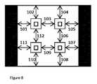
図8は本発明の実施形態に係る画素の4タップトポロジーを示す。タップを複数の対称軸を画定するように空間的に編成することができる。タップを距離101〜102が略等しくなるように、画素の内部に空間的に編成することができる。これらの距離は、コンポーネント間に利用可能な光学領域によって画定することができる。例えば、タップの検出領域間の距離103、106、109、および112は略等しくすることができる。さらに、検出領域と最近接周囲回路構成との間の距離102、104、105、107、108、110、111、101、および102もまた、略等しくすることができる。画素の内部に複数の対称軸を画定するようにタップを空間的に編成することは好都合である。実際、タップは光学領域の均等面に関連付けられ、周囲回路構成から同等の影響を受ける。この空間編成は、シーンから反射する略等しい変調信号を測定することを可能にする。換言すると、この空間編成は、Sφに略等しい4つの信号Sφ1〜Sφ4を測定することを可能にする。FIG. 8 illustrates a 4-tap topology of pixels according to an embodiment of the present invention. The taps can be spatially knitted to define a plurality of axes of symmetry. Taps can be spatially organized within the pixels so that the distances 101-102 are substantially equal. These distances can be defined by the optical area available between the components. For example, the
図9は本発明のさらなる実施形態に係る画素の4タップトポロジーを示す。ToFシステムの撮像センサは八角形の画素を含むことができる。各画素は、回路構成605、606、607、および608によって囲まれた4つのタップ601、602、603、および604を含むことができる。画素の八角形の形状は好都合となりうる。この特定の形状は、使用される基板の表面および画素の光学領域を最適化しながら、幾つかの画素およびタップの間で回路構成を共有することを可能にする。八角形の形状はまた、画素の内部に幾つかの対称軸を画定することをも可能にし、それは、シーンから反射した変調信号をより正確に測定するのを助ける。 FIG. 9 shows a 4-tap topology of pixels according to a further embodiment of the invention. The imaging sensor of the ToF system can include octagonal pixels. Each pixel can include four
本発明はまた、少なくとも1つの画素を含む撮像センサを有する飛行時間システムを駆動するための方法に関し、前記画素が駆動信号によって駆動される複数のタップを含み、飛行時間システムが、変調信号によりシーンを照明するように適応された照明システムと共に使用するためのものであり、前記方法は、各画素に対し、少なくとも第1の組および第2の組のタップを決定するステップと、各組のタップを駆動して、変調信号の所定数N周期中にシーンから反射される変調信号を検出するステップとを含む。 The present invention also relates to a method for driving a time-of-flight system having an imaging sensor including at least one pixel, wherein the pixel includes a plurality of taps driven by a drive signal, the time-of-flight system being a scene with a modulation signal. Determining at least a first set and a second set of taps for each pixel, and each set of taps for use with an illumination system adapted to illuminate And detecting a modulation signal reflected from the scene during a predetermined number N of modulation signals.
例証のために、該方法について、タップ1〜タップ4で表される4つのタップを含む4タップ画素に関連して説明するが、該方法はそれに限定されない。 For purposes of illustration, the method will be described in the context of a 4-tap pixel that includes four taps represented by
図10は、該方法の第2ステップ中にタップを駆動するために使用される駆動信号の例を示し、ここでNは2に等しい。この図では、変調信号16は、「光」と呼ばれる信号によって表される。 FIG. 10 shows an example of a drive signal used to drive the tap during the second step of the method, where N is equal to 2. In this figure, the
方法の第1ステップに従って、第1の組および第2の組のタップは、それぞれ(タップ1、タップ2)および(タップ3、タップ4)と決定される。 According to the first step of the method, the first set and the second set of taps are determined as (
方法の第2ステップに従って、第1の組および第2の組のタップ、すなわちそれぞれ(タップ1、タップ2)および(タップ3、タップ4)は、変調信号の2周期中にシーンから反射する変調信号17を検出するように駆動される。 According to the second step of the method, the first set and the second set of taps, ie (
好ましくは、1組のうちの第1タップは第1駆動信号によって駆動され、この組のうちの第2タップは、第1駆動信号の反転信号である第2駆動信号によって駆動される。これは図10によって示され、ここでタップ1およびタップ2(それぞれタップ3およびタップ4)の駆動信号は反転している。すなわち、第2駆動信号は第1駆動信号と比較して180°位相シフトしている。 Preferably, the first tap of the set is driven by the first drive signal, and the second tap of the set is driven by the second drive signal that is an inverted signal of the first drive signal. This is illustrated by FIG. 10, where the drive signals for
さらにいっそう好ましくは、第1の組のタップの第1駆動信号は、照明部によって送信された変調信号16のN周期分に対応し、第2の組のタップの第1駆動信号は、照明部によって送信された変調信号16と比較して90°位相シフトした信号のN周期分に対応する。 Even more preferably, the first drive signal of the first set of taps corresponds to N periods of the modulated
この実施形態もまた図10によって示される。実際、タップ1の駆動信号は変調信号16(または「光」)の2周期分に対応し、タップ3の駆動信号は、変調信号16と比較して90°位相シフトした信号の2周期分に対応する。 This embodiment is also illustrated by FIG. In fact, the drive signal for
この特定の実施例では、タップ1、タップ2、タップ3、およびタップ4に送信された駆動信号は、照明部によって送信された変調信号と比較してそれぞれ0°、180°、90°、および270°位相シフトした信号の2周期分に対応する。 In this particular example, the drive signals transmitted to tap 1, tap 2, tap 3, and tap 4 are 0 °, 180 °, 90 °, respectively, compared to the modulation signal transmitted by the illuminator. This corresponds to two periods of the signal shifted by 270 °.
1画素当たりY個のタップの組の場合、yを0から(Y−1)までの範囲として、組(対)「y」の駆動信号と照明部によって送信された変調信号との間の位相シフトは、その次の各組に対し、例えばy*180°/Yとすることができる。 In the case of a set of Y taps per pixel, the phase between the drive signal of the pair (pair) “y” and the modulation signal transmitted by the illumination unit, where y ranges from 0 to (Y−1) The shift can be, for example, y * 180 ° / Y for each subsequent set.
この特定の例では、第1の1組のタップは、それらのそれぞれの駆動信号後に2周期中の反射変調光17を検出することができ、次いで、順次、第2の1組のタップはそれらのそれぞれの駆動信号後の2周期中の反射変調光17を検出することができる。タップを1組ずつ駆動することは、駆動信号間の重複を回避することを可能にする。これは、1つの画素内で一度に作動するタップは1つだけであり、その間、他のタップは作動しないことを意味する。これは図10によって明瞭に示される。この方法のおかげで、タップに要求される帯域幅を低減し、かつ駆動信号のデューティサイクルの低減を回避することが可能である。 In this particular example, the first set of taps can detect the reflected modulated light 17 in two periods after their respective drive signals, and then in turn the second set of taps It is possible to detect the reflected modulated light 17 in two periods after each of the drive signals. Driving the taps one by one makes it possible to avoid duplication between drive signals. This means that only one tap is active at a time within one pixel, while the other taps are not active during that time. This is clearly shown by FIG. Thanks to this method, it is possible to reduce the bandwidth required for the tap and to avoid a reduction in the duty cycle of the drive signal.
さらなる実施形態では、飛行時間システムはさらに、基準信号とシーンからの反射変調信号17との間の相関測定を決定するように適応することができる。該方法はさらに、決定された各タップの組に対し、シーンからの反射変調信号17とそれぞれ第1および第2基準信号との間で第1および第2相関測定を決定するステップを含むことができる。 In a further embodiment, the time-of-flight system can be further adapted to determine a correlation measurement between the reference signal and the reflected
第1の1組のタップについては、第1基準信号は、照明部によって送信された変調信号16に対応することができ、第2基準信号は第1基準信号の反転信号とすることができる。 For the first set of taps, the first reference signal can correspond to the modulated
第2の1組のタップについては、第1基準信号は、照明部によって送信された変調信号16と比較して90°位相シフトした信号に対応することができ、第2基準信号は第1基準信号の反転信号とすることができる。 For the second set of taps, the first reference signal can correspond to a signal that is 90 ° phase shifted compared to the modulated
先に導入した表記法を参照することによって、タップ1は、照明部によって送信された変調信号16の2周期分である駆動信号によって駆動されることができ、タップ2は、照明部によって送信された変調信号16と比較して180°位相シフトした信号の2周期分である駆動信号によって駆動されることができる。さらに、第1の組(対)のタップ(タップ1、タップ2)は、シーンから反射した変調信号17(すなわちSφ)と基準信号SIおよび
同様に、タップ3は、照明部によって送信された変調信号と比較して90°位相シフトした信号の2周期分である駆動信号によって駆動することができ、タップ4は、照明部によって送信された変調信号と比較して270°位相シフトした信号の2周期分である駆動信号によって駆動することができる。さらに、第2の組(対)のタップ(タップ3、タップ4)は、シーンから反射した変調信号17(すなわちSφ)と基準信号SQおよび
この方法は、4つのタップによってSφを略同時に測定することを可能にし、それは測度の精度および信頼性を高め、かつ移動頑健性を可能にする。好ましくは、高い移動頑健性を確実にするために、組(対)の各駆動間の時間間隔はできるだけ短くすべきであり、例えば変調光16の8周期分の期間未満とすべきである。好ましくは、駆動は交互に行うことができる。すなわち、第1の組のタップを最初に駆動することができ、次いで第2の組のタップを駆動することができ、次いで第1組のタップを再び駆動することができる。検出は、周期的に各組に対しN周期後に継続することができる。This method allowsSφ to be measured almost simultaneously by four taps, which increases the accuracy and reliability of the measure and allows for movement robustness. Preferably, in order to ensure high mobility robustness, the time interval between each drive of the pair (pair) should be as short as possible, for example, less than a period of 8 periods of the modulated
撮像センサが図4に示すように幾つかの画素を含む場合、1組のタップに送信される駆動信号は同時であってよいことを理解されたい。例えばタップ1に送信される駆動信号は、前に定義したように上タップに送信される信号に対応することができ、タップ2に送信される駆動信号は、下タップに送信される信号に対応することができ、タップ3に送信される駆動信号は、右タップに送信される信号に対応することができ、タップ4に送信される駆動信号は、左タップに送信される信号に対応することができる。 It should be understood that if the imaging sensor includes several pixels as shown in FIG. 4, the drive signals transmitted to the set of taps may be simultaneous. For example, the drive signal sent to tap 1 can correspond to the signal sent to the upper tap as previously defined, and the drive signal sent to tap 2 corresponds to the signal sent to the lower tap. The drive signal transmitted to tap 3 can correspond to the signal transmitted to the right tap, and the drive signal transmitted to tap 4 can correspond to the signal transmitted to the left tap. Can do.
さらに、第1の組のタップは(上タップ、下タップ)とすることができ、第2の組のタップは(右タップ、左タップ)とすることができる。好ましくは、1組のタップに含まれるタップは、画素における対向位置を有する。例えば、タップが画素に正方形を形成する場合、1組のタップに含まれるタップは、対角位置に配置されるタップとなる。1組のタップに属するタップは同一画素に属することができる。 Furthermore, the first set of taps can be (upper tap, lower tap), and the second set of taps can be (right tap, left tap). Preferably, the taps included in the set of taps have opposing positions in the pixels. For example, when a tap forms a square in a pixel, a tap included in one set of taps is a tap arranged at a diagonal position. Taps belonging to one set of taps can belong to the same pixel.
上、下、右、および左という用語は制限的用語ではなく、明確を期すために使用するものであることを理解されたい。 It should be understood that the terms top, bottom, right, and left are not limiting terms and are used for clarity.
Claims (16)
Translated fromJapanese前記ToFシステムが少なくとも1つの画素(35a)を含む撮像センサ(35)を有し、
前記画素が、前記シーンから反射した変調信号(17)を検出するために駆動信号によって駆動されるタップを含み、
各画素に対し、
・少なくとも第1の組、および第2の組のタップを決定するステップと、
・各タップの組を駆動して、前記変調信号(16)の所定数N周期中に前記反射した変調信号(17)を検出するステップと、
を含む方法。A method for driving a time-of-flight (ToF) system (3) for a lighting system (18) adapted to illuminate a scene (15) with a modulation signal (16), comprising:
The ToF system comprises an imaging sensor (35) comprising at least one pixel (35a);
The pixel includes a tap driven by a drive signal to detect a modulated signal (17) reflected from the scene;
For each pixel
Determining at least a first set and a second set of taps;
Driving each set of taps to detect the reflected modulated signal (17) during a predetermined number N periods of the modulated signal (16);
Including methods.
‐決定された各タップの組に対し、前記シーンから反射した変調信号(17)とそれぞれ第1および第2基準信号との間の第1および第2相関の測定を決定するステップを含む、請求項1〜5のいずれか一項に記載の方法。The time-of-flight system is further adapted to determine a measure of correlation between a reference signal and a modulation signal (17) reflected from the scene, the method further comprising:
-Determining, for each determined set of taps, a measurement of the first and second correlations between the modulated signal (17) reflected from the scene and the first and second reference signals, respectively. Item 6. The method according to any one of Items 1 to 5.
・前記第2の1組のタップの場合、前記第1基準信号は、前記照明部によって送信された前記変調信号(16)と比較して90°位相がシフトした信号に対応し、前記第2基準信号は前記第1基準信号の反転信号である、
請求項6に記載の方法。In the case of the first set of taps, the first reference signal corresponds to the modulation signal (16) transmitted by the illumination unit, and the second reference signal is an inverted signal of the first reference signal And
In the case of the second set of taps, the first reference signal corresponds to a signal whose phase is shifted by 90 ° compared to the modulation signal (16) transmitted by the illumination unit, The reference signal is an inverted signal of the first reference signal.
The method of claim 6.
・少なくとも2つの画素(35a)を含み、各画素にタップが含まれる、撮像センサ(35)と、
・前記タップを駆動するために駆動信号を発生するための信号発生器(30、501)と、
・前記信号発生器(501、30)から前記駆動信号を受信し、かつそれらを前記タップに送信するように適応されたタップドライバ(31a、31b、32a、32b、502、503、504、505)とを備え、
・各画素が少なくとも2組のタップを含むこと、
・各画素の前記2組のタップがそれぞれ異なるドライバに接続されること、および
・各ドライバが各画素の1つのタップに接続され、前記各ドライバに接続された前記撮像センサの前記画素のタップが1組のタップを形成することを特徴とする、飛行時間システム(3)。A time-of-flight system (3) for a lighting system (18) adapted to illuminate a scene (15) with a modulated signal (16),
An imaging sensor (35) comprising at least two pixels (35a), each pixel including a tap;
A signal generator (30, 501) for generating a drive signal to drive the tap;
Tap drivers (31a, 31b, 32a, 32b, 502, 503, 504, 505) adapted to receive the drive signals from the signal generator (501, 30) and send them to the tap And
Each pixel contains at least two sets of taps,
The two sets of taps of each pixel are connected to different drivers, and each driver is connected to one tap of each pixel, and the taps of the pixels of the imaging sensor connected to the drivers are Time-of-flight system (3), characterized in that it forms a set of taps.
Applications Claiming Priority (3)
| Application Number | Priority Date | Filing Date | Title |
|---|---|---|---|
| EP14150922.4 | 2014-01-13 | ||
| EP14150922.4AEP2894492B1 (en) | 2014-01-13 | 2014-01-13 | A method for driving a time-of-flight system |
| PCT/EP2015/050195WO2015104307A1 (en) | 2014-01-13 | 2015-01-08 | A method for driving a time-of-flight system |
Publications (2)
| Publication Number | Publication Date |
|---|---|
| JP2016527482Atrue JP2016527482A (en) | 2016-09-08 |
| JP6529487B2 JP6529487B2 (en) | 2019-06-12 |
Family
ID=49955917
Family Applications (1)
| Application Number | Title | Priority Date | Filing Date |
|---|---|---|---|
| JP2016518541AExpired - Fee RelatedJP6529487B2 (en) | 2014-01-13 | 2015-01-08 | Method for driving a time of flight system |
Country Status (7)
| Country | Link |
|---|---|
| US (1) | US10509126B2 (en) |
| EP (2) | EP3792662A1 (en) |
| JP (1) | JP6529487B2 (en) |
| KR (1) | KR20160032014A (en) |
| CN (1) | CN105518485B (en) |
| BE (1) | BE1022490B1 (en) |
| WO (1) | WO2015104307A1 (en) |
Cited By (2)
| Publication number | Priority date | Publication date | Assignee | Title |
|---|---|---|---|---|
| WO2019044569A1 (en)* | 2017-08-30 | 2019-03-07 | ソニーセミコンダクタソリューションズ株式会社 | Image-capturing element and image-capturing device |
| JP2020010328A (en)* | 2018-07-09 | 2020-01-16 | 三星電子株式会社Samsung Electronics Co.,Ltd. | Image sensor |
Families Citing this family (41)
| Publication number | Priority date | Publication date | Assignee | Title |
|---|---|---|---|---|
| TWI694604B (en) | 2015-07-23 | 2020-05-21 | 光澄科技股份有限公司 | Light detector |
| US10707260B2 (en) | 2015-08-04 | 2020-07-07 | Artilux, Inc. | Circuit for operating a multi-gate VIS/IR photodiode |
| US10761599B2 (en) | 2015-08-04 | 2020-09-01 | Artilux, Inc. | Eye gesture tracking |
| US10861888B2 (en) | 2015-08-04 | 2020-12-08 | Artilux, Inc. | Silicon germanium imager with photodiode in trench |
| CN108028258B (en) | 2015-08-04 | 2022-06-21 | 光程研创股份有限公司 | Germanium-silicon photosensitive equipment |
| EP3783656B1 (en) | 2015-08-27 | 2023-08-23 | Artilux Inc. | Wide spectrum optical sensor |
| US10739443B2 (en) | 2015-11-06 | 2020-08-11 | Artilux, Inc. | High-speed light sensing apparatus II |
| US10418407B2 (en) | 2015-11-06 | 2019-09-17 | Artilux, Inc. | High-speed light sensing apparatus III |
| US10741598B2 (en) | 2015-11-06 | 2020-08-11 | Atrilux, Inc. | High-speed light sensing apparatus II |
| US10886309B2 (en) | 2015-11-06 | 2021-01-05 | Artilux, Inc. | High-speed light sensing apparatus II |
| US10254389B2 (en) | 2015-11-06 | 2019-04-09 | Artilux Corporation | High-speed light sensing apparatus |
| EP3193190B1 (en)* | 2016-01-15 | 2023-04-12 | Sony Depthsensing Solutions N.V. | A detector device with majority current and a circuitry for controlling the current |
| EP3193369B1 (en)* | 2016-01-15 | 2021-11-17 | Sony Depthsensing Solutions N.V. | A detector device with majority current and isolation means |
| CN107851656B (en) | 2016-03-04 | 2022-12-16 | 索尼公司 | Camera and distance measuring system |
| US10557925B2 (en)* | 2016-08-26 | 2020-02-11 | Samsung Electronics Co., Ltd. | Time-of-flight (TOF) image sensor using amplitude modulation for range measurement |
| WO2018100082A1 (en) | 2016-11-30 | 2018-06-07 | Sony Semiconductor Solutions Corporation | Apparatus and method |
| WO2018104464A1 (en)* | 2016-12-07 | 2018-06-14 | Sony Semiconductor Solutions Corporation | Apparatus and method |
| US11592536B2 (en) | 2018-01-10 | 2023-02-28 | Sony Semiconductor Solutions Corporation | Control of image capture |
| US10777692B2 (en) | 2018-02-23 | 2020-09-15 | Artilux, Inc. | Photo-detecting apparatus and photo-detecting method thereof |
| US11482553B2 (en) | 2018-02-23 | 2022-10-25 | Artilux, Inc. | Photo-detecting apparatus with subpixels |
| US11105928B2 (en) | 2018-02-23 | 2021-08-31 | Artilux, Inc. | Light-sensing apparatus and light-sensing method thereof |
| CN114335030A (en) | 2018-04-08 | 2022-04-12 | 奥特逻科公司 | Optical detection device |
| US10854770B2 (en) | 2018-05-07 | 2020-12-01 | Artilux, Inc. | Avalanche photo-transistor |
| US10969877B2 (en) | 2018-05-08 | 2021-04-06 | Artilux, Inc. | Display apparatus |
| KR102534247B1 (en) | 2018-10-01 | 2023-05-18 | 삼성전자주식회사 | 3D(dimension) image sensor comprising polarizer, and depth calibrating method and 3D image generating method based on the 3D image sensor |
| KR102562360B1 (en)* | 2018-10-05 | 2023-08-02 | 엘지이노텍 주식회사 | Method and camera module for acquiring depth information |
| KR102683411B1 (en)* | 2018-10-05 | 2024-07-10 | 삼성전자주식회사 | Image sensor and image processing system with pixel structure to improve demodulation contrast performance |
| US11506763B2 (en) | 2018-10-31 | 2022-11-22 | Infineon Technologies Ag | Image sensor with interleaved hold for single-readout depth measurement |
| US11574942B2 (en) | 2018-12-12 | 2023-02-07 | Artilux, Inc. | Semiconductor device with low dark noise |
| US11798960B2 (en)* | 2019-03-13 | 2023-10-24 | Sony Semiconductor Solutions Corporation | Processing circuit and method for time-of-flight image sensor |
| WO2020193161A1 (en)* | 2019-03-25 | 2020-10-01 | Sony Semiconductor Solutions Corporation | Time-of-flight apparatus and method |
| US12085410B2 (en) | 2019-05-24 | 2024-09-10 | Sony Semiconductor Solutions Corporation | Solid-state imaging device and distance measurement device |
| CN110320528B (en)* | 2019-06-14 | 2021-04-30 | 奥比中光科技集团股份有限公司 | Time depth camera and noise reduction distance measurement method for multi-frequency modulation and demodulation |
| CN110361751B (en)* | 2019-06-14 | 2021-04-30 | 奥比中光科技集团股份有限公司 | Time flight depth camera and distance measuring method for reducing noise of single-frequency modulation and demodulation |
| TWI853067B (en) | 2019-08-21 | 2024-08-21 | 荷蘭商露明控股公司 | Infrared imaging assembly, method of generating a depth map for a scene using an infrared imaging assembly, and camera |
| US12278252B2 (en) | 2019-08-28 | 2025-04-15 | Artilux, Inc. | Photo-detecting apparatus with low dark current |
| CN116504856A (en) | 2019-08-28 | 2023-07-28 | 光程研创股份有限公司 | Photodetection device with low dark current |
| DE102019131988A1 (en) | 2019-11-26 | 2021-05-27 | Sick Ag | 3D time-of-flight camera and method for capturing three-dimensional image data |
| US11205279B2 (en)* | 2019-12-13 | 2021-12-21 | Sony Semiconductor Solutions Corporation | Imaging devices and decoding methods thereof |
| KR20210151497A (en)* | 2020-06-05 | 2021-12-14 | 에스케이하이닉스 주식회사 | Image Sensing Device |
| KR20220010192A (en)* | 2020-07-17 | 2022-01-25 | 삼성전자주식회사 | Multi-function time-of-flight sensor and method of operating the same |
Citations (5)
| Publication number | Priority date | Publication date | Assignee | Title |
|---|---|---|---|---|
| JP2000517427A (en)* | 1996-09-05 | 2000-12-26 | ルドルフ シュヴァルト | Method and apparatus for examining phase and / or amplitude information of an electromagnetic wave |
| WO2008047640A1 (en)* | 2006-10-18 | 2008-04-24 | Panasonic Electric Works Co., Ltd. | Spatial information detecting device |
| JP2010537555A (en)* | 2007-08-23 | 2010-12-02 | イーストマン コダック カンパニー | Image sensor with color filter array with panchromatic checkerboard pattern |
| JP2011013138A (en)* | 2009-07-03 | 2011-01-20 | Toyota Central R&D Labs Inc | Image sensor and light receiving device used for the image sensor |
| WO2011158796A1 (en)* | 2010-06-14 | 2011-12-22 | パナソニック電工株式会社 | Drive device and spatial information detector device employing same |
Family Cites Families (4)
| Publication number | Priority date | Publication date | Assignee | Title |
|---|---|---|---|---|
| DK1513202T3 (en) | 2003-09-02 | 2010-05-10 | Univ Bruxelles | Detector for electromagnetic radiation using a majority current |
| JP5171158B2 (en) | 2007-08-22 | 2013-03-27 | 浜松ホトニクス株式会社 | Solid-state imaging device and range image measuring device |
| CN102027388B (en) | 2008-04-11 | 2013-08-28 | 瑞士联邦理工大学,洛桑(Epfl) | Time-of-flight based imaging system using a display as illumination source |
| CN105026955B (en) | 2012-12-28 | 2018-12-18 | 诺基亚技术有限公司 | For to the method and apparatus for answering the data of camera to carry out noise reduction from distance perception |
- 2014
- 2014-01-13EPEP20201875.0Apatent/EP3792662A1/ennot_activeWithdrawn
- 2014-01-13EPEP14150922.4Apatent/EP2894492B1/enactiveActive
- 2014-02-28BEBE2014/0136Apatent/BE1022490B1/ennot_activeIP Right Cessation
- 2015
- 2015-01-08USUS14/897,275patent/US10509126B2/enactiveActive
- 2015-01-08KRKR1020157035188Apatent/KR20160032014A/ennot_activeCeased
- 2015-01-08WOPCT/EP2015/050195patent/WO2015104307A1/enactiveApplication Filing
- 2015-01-08JPJP2016518541Apatent/JP6529487B2/ennot_activeExpired - Fee Related
- 2015-01-08CNCN201580001003.XApatent/CN105518485B/ennot_activeExpired - Fee Related
Patent Citations (5)
| Publication number | Priority date | Publication date | Assignee | Title |
|---|---|---|---|---|
| JP2000517427A (en)* | 1996-09-05 | 2000-12-26 | ルドルフ シュヴァルト | Method and apparatus for examining phase and / or amplitude information of an electromagnetic wave |
| WO2008047640A1 (en)* | 2006-10-18 | 2008-04-24 | Panasonic Electric Works Co., Ltd. | Spatial information detecting device |
| JP2010537555A (en)* | 2007-08-23 | 2010-12-02 | イーストマン コダック カンパニー | Image sensor with color filter array with panchromatic checkerboard pattern |
| JP2011013138A (en)* | 2009-07-03 | 2011-01-20 | Toyota Central R&D Labs Inc | Image sensor and light receiving device used for the image sensor |
| WO2011158796A1 (en)* | 2010-06-14 | 2011-12-22 | パナソニック電工株式会社 | Drive device and spatial information detector device employing same |
Cited By (10)
| Publication number | Priority date | Publication date | Assignee | Title |
|---|---|---|---|---|
| WO2019044569A1 (en)* | 2017-08-30 | 2019-03-07 | ソニーセミコンダクタソリューションズ株式会社 | Image-capturing element and image-capturing device |
| CN109729759A (en)* | 2017-08-30 | 2019-05-07 | 索尼半导体解决方案公司 | Imaging elements and imaging devices |
| KR102061467B1 (en) | 2017-08-30 | 2019-12-31 | 소니 세미컨덕터 솔루션즈 가부시키가이샤 | Imaging Device and Imaging Device |
| US10636831B2 (en) | 2017-08-30 | 2020-04-28 | Sony Semiconductor Solutions Corporation | Imaging element and imaging apparatus |
| JPWO2019044569A1 (en)* | 2017-08-30 | 2020-08-06 | ソニーセミコンダクタソリューションズ株式会社 | Imaging device and imaging device |
| CN109729759B (en)* | 2017-08-30 | 2021-09-17 | 索尼半导体解决方案公司 | Imaging element and imaging device |
| JP7013448B2 (en) | 2017-08-30 | 2022-01-31 | ソニーセミコンダクタソリューションズ株式会社 | Image sensor and image sensor |
| US11309346B2 (en) | 2017-08-30 | 2022-04-19 | Sony Semiconductor Solutions Corporation | Imaging element and imaging apparatus |
| JP2020010328A (en)* | 2018-07-09 | 2020-01-16 | 三星電子株式会社Samsung Electronics Co.,Ltd. | Image sensor |
| JP7442982B2 (en) | 2018-07-09 | 2024-03-05 | 三星電子株式会社 | image sensor |
Also Published As
| Publication number | Publication date |
|---|---|
| CN105518485A (en) | 2016-04-20 |
| BE1022490B1 (en) | 2016-05-04 |
| EP2894492A1 (en) | 2015-07-15 |
| EP3792662A1 (en) | 2021-03-17 |
| US20160306045A1 (en) | 2016-10-20 |
| KR20160032014A (en) | 2016-03-23 |
| JP6529487B2 (en) | 2019-06-12 |
| WO2015104307A1 (en) | 2015-07-16 |
| US10509126B2 (en) | 2019-12-17 |
| EP2894492B1 (en) | 2020-10-28 |
| CN105518485B (en) | 2018-11-13 |
Similar Documents
| Publication | Publication Date | Title |
|---|---|---|
| JP6529487B2 (en) | Method for driving a time of flight system | |
| US11448757B2 (en) | Distance measuring device | |
| US10101453B2 (en) | Time of flight apparatuses and an illumination source | |
| US11067675B2 (en) | Time of flight imaging apparatuses and a method for adjusting a reference frequency | |
| US11408983B2 (en) | Lidar 2D receiver array architecture | |
| JP5593479B2 (en) | TOF region advantageous for suppression of background radiation | |
| US20160112696A1 (en) | Imaging apparatuses and a time of flight imaging method | |
| KR101020999B1 (en) | Photographing device and image control method thereof | |
| KR20210031710A (en) | Electronic device and method | |
| WO2010098454A1 (en) | Distance measuring apparatus | |
| CN113030999B (en) | Time-of-flight sensing system and image sensor for use therein | |
| CN100573187C (en) | Range image sensor | |
| CN112946686A (en) | Time-of-flight sensing system and image sensor used therein | |
| US20210405192A1 (en) | Time-of-flight based distance measuring method and related distance measuring system | |
| US20220252730A1 (en) | Time-of-flight imaging apparatus and time-of-flight imaging method | |
| JP2022165344A (en) | Distance measuring device and distance measuring system | |
| TWI897871B (en) | Time of flight sensing system and image sensor used therein | |
| US20240129630A1 (en) | Image-capturing system, image-capturing device, and image-capturing method | |
| US20200309956A1 (en) | Imaging portion, time-of-flight device and method | |
| JP2022166834A (en) | Depth sensor and method of operation | |
| WO2022176498A1 (en) | Ranging sensor and ranging device |
Legal Events
| Date | Code | Title | Description |
|---|---|---|---|
| A621 | Written request for application examination | Free format text:JAPANESE INTERMEDIATE CODE: A621 Effective date:20151214 | |
| A131 | Notification of reasons for refusal | Free format text:JAPANESE INTERMEDIATE CODE: A131 Effective date:20161122 | |
| A601 | Written request for extension of time | Free format text:JAPANESE INTERMEDIATE CODE: A601 Effective date:20170217 | |
| A521 | Request for written amendment filed | Free format text:JAPANESE INTERMEDIATE CODE: A523 Effective date:20170421 | |
| RD03 | Notification of appointment of power of attorney | Free format text:JAPANESE INTERMEDIATE CODE: A7423 Effective date:20170706 | |
| RD04 | Notification of resignation of power of attorney | Free format text:JAPANESE INTERMEDIATE CODE: A7424 Effective date:20170710 | |
| A02 | Decision of refusal | Free format text:JAPANESE INTERMEDIATE CODE: A02 Effective date:20170912 | |
| A521 | Request for written amendment filed | Free format text:JAPANESE INTERMEDIATE CODE: A523 Effective date:20171129 | |
| A911 | Transfer to examiner for re-examination before appeal (zenchi) | Free format text:JAPANESE INTERMEDIATE CODE: A911 Effective date:20171206 | |
| A912 | Re-examination (zenchi) completed and case transferred to appeal board | Free format text:JAPANESE INTERMEDIATE CODE: A912 Effective date:20180119 | |
| A521 | Request for written amendment filed | Free format text:JAPANESE INTERMEDIATE CODE: A523 Effective date:20180927 | |
| A711 | Notification of change in applicant | Free format text:JAPANESE INTERMEDIATE CODE: A712 Effective date:20181212 | |
| A521 | Request for written amendment filed | Free format text:JAPANESE INTERMEDIATE CODE: A523 Effective date:20190110 | |
| RD04 | Notification of resignation of power of attorney | Free format text:JAPANESE INTERMEDIATE CODE: A7424 Effective date:20190208 | |
| A521 | Request for written amendment filed | Free format text:JAPANESE INTERMEDIATE CODE: A523 Effective date:20190213 | |
| RD03 | Notification of appointment of power of attorney | Free format text:JAPANESE INTERMEDIATE CODE: A7423 Effective date:20190514 | |
| A61 | First payment of annual fees (during grant procedure) | Free format text:JAPANESE INTERMEDIATE CODE: A61 Effective date:20190514 | |
| R150 | Certificate of patent or registration of utility model | Ref document number:6529487 Country of ref document:JP Free format text:JAPANESE INTERMEDIATE CODE: R150 | |
| RD04 | Notification of resignation of power of attorney | Free format text:JAPANESE INTERMEDIATE CODE: A7424 Effective date:20190530 | |
| LAPS | Cancellation because of no payment of annual fees |