JP2016171330A - Manufacturing method for semiconductor device - Google Patents
Manufacturing method for semiconductor deviceDownload PDFInfo
- Publication number
- JP2016171330A JP2016171330AJP2016086671AJP2016086671AJP2016171330AJP 2016171330 AJP2016171330 AJP 2016171330AJP 2016086671 AJP2016086671 AJP 2016086671AJP 2016086671 AJP2016086671 AJP 2016086671AJP 2016171330 AJP2016171330 AJP 2016171330A
- Authority
- JP
- Japan
- Prior art keywords
- film
- transistor
- oxide semiconductor
- oxygen
- substrate
- Prior art date
- Legal status (The legal status is an assumption and is not a legal conclusion. Google has not performed a legal analysis and makes no representation as to the accuracy of the status listed.)
- Granted
Links
Images


Classifications
- H—ELECTRICITY
- H10—SEMICONDUCTOR DEVICES; ELECTRIC SOLID-STATE DEVICES NOT OTHERWISE PROVIDED FOR
- H10D—INORGANIC ELECTRIC SEMICONDUCTOR DEVICES
- H10D30/00—Field-effect transistors [FET]
- H10D30/60—Insulated-gate field-effect transistors [IGFET]
- H10D30/67—Thin-film transistors [TFT]
- H10D30/6729—Thin-film transistors [TFT] characterised by the electrodes
- H10D30/6737—Thin-film transistors [TFT] characterised by the electrodes characterised by the electrode materials
- H10D30/6739—Conductor-insulator-semiconductor electrodes
- H—ELECTRICITY
- H10—SEMICONDUCTOR DEVICES; ELECTRIC SOLID-STATE DEVICES NOT OTHERWISE PROVIDED FOR
- H10D—INORGANIC ELECTRIC SEMICONDUCTOR DEVICES
- H10D30/00—Field-effect transistors [FET]
- H10D30/60—Insulated-gate field-effect transistors [IGFET]
- H10D30/67—Thin-film transistors [TFT]
- H10D30/6704—Thin-film transistors [TFT] having supplementary regions or layers in the thin films or in the insulated bulk substrates for controlling properties of the device
- H—ELECTRICITY
- H10—SEMICONDUCTOR DEVICES; ELECTRIC SOLID-STATE DEVICES NOT OTHERWISE PROVIDED FOR
- H10D—INORGANIC ELECTRIC SEMICONDUCTOR DEVICES
- H10D30/00—Field-effect transistors [FET]
- H10D30/60—Insulated-gate field-effect transistors [IGFET]
- H10D30/67—Thin-film transistors [TFT]
- H10D30/674—Thin-film transistors [TFT] characterised by the active materials
- H10D30/6755—Oxide semiconductors, e.g. zinc oxide, copper aluminium oxide or cadmium stannate
- H—ELECTRICITY
- H10—SEMICONDUCTOR DEVICES; ELECTRIC SOLID-STATE DEVICES NOT OTHERWISE PROVIDED FOR
- H10D—INORGANIC ELECTRIC SEMICONDUCTOR DEVICES
- H10D99/00—Subject matter not provided for in other groups of this subclass
Landscapes
- Thin Film Transistor (AREA)
- Devices For Indicating Variable Information By Combining Individual Elements (AREA)
- Electroluminescent Light Sources (AREA)
- Solid State Image Pick-Up Elements (AREA)
- Semiconductor Memories (AREA)
- Physical Vapour Deposition (AREA)
- Non-Volatile Memory (AREA)
- Metal-Oxide And Bipolar Metal-Oxide Semiconductor Integrated Circuits (AREA)
Abstract
Description
Translated fromJapanese半導体装置および半導体装置の作製方法に関する。 The present invention relates to a semiconductor device and a method for manufacturing the semiconductor device.
なお、本明細書中において半導体装置とは、半導体特性を利用することで機能しうる装
置全般を指し、電気光学装置、半導体回路および電子機器は全て半導体装置である。Note that in this specification, a semiconductor device refers to all devices that can function by utilizing semiconductor characteristics, and an electro-optical device, a semiconductor circuit, and an electronic device are all semiconductor devices.
絶縁表面を有する基板上に形成された半導体薄膜を用いてトランジスタを構成する技術
が注目されている。該トランジスタは集積回路(IC)や画像表示装置(表示装置)のよ
うな電子デバイスに広く応用されている。トランジスタに適用可能な半導体薄膜としてシ
リコン系半導体材料が広く知られているが、その他の材料として酸化物半導体が注目され
ている。A technique for forming a transistor using a semiconductor thin film formed over a substrate having an insulating surface has attracted attention. The transistor is widely applied to electronic devices such as an integrated circuit (IC) and an image display device (display device). A silicon-based semiconductor material is widely known as a semiconductor thin film applicable to a transistor, but an oxide semiconductor has attracted attention as another material.
例えば、トランジスタの活性層として、電子キャリア濃度が1018/cm3未満であ
るインジウム(In)、ガリウム(Ga)、および亜鉛(Zn)を含む非晶質酸化物を用
いたトランジスタが開示されている(特許文献1参照)。For example, a transistor using an amorphous oxide containing indium (In), gallium (Ga), and zinc (Zn) having an electron carrier concentration of less than 1018 / cm3 as an active layer of the transistor is disclosed. (See Patent Document 1).
しかし、酸化物半導体を有する半導体デバイスにおいて、該酸化物半導体が酸素欠損や
水分、水素などを有すると、その電気伝導度が変化する恐れがある。このような現象は、
酸化物半導体を用いたトランジスタにとって電気的特性の変動要因となる。However, in a semiconductor device including an oxide semiconductor, if the oxide semiconductor has oxygen deficiency, moisture, hydrogen, or the like, the electrical conductivity may change. Such a phenomenon
For a transistor including an oxide semiconductor, this is a factor of variation in electrical characteristics.
このような問題に鑑み、酸化物半導体を用いた半導体装置に安定した電気的特性を付与
し、信頼性の高い半導体装置を提供することを目的の一とする。また、酸化物半導体を有
する半導体デバイスのオフ電流が極めて低い(ヨクトアンペア(yA)レベル)という特
性を利用し、新しいエレクトロニクスの分野として、ヨクトロニクス(Yoctoron
ics(Yocto Ampere Electronics)、ヨクトアンペアの電流
を扱うエレクトロニクス)というものを確立し、提供することを目的の一とする。In view of such a problem, an object is to provide a highly reliable semiconductor device by imparting stable electrical characteristics to a semiconductor device including an oxide semiconductor. In addition, by utilizing the characteristic that the off-state current of a semiconductor device including an oxide semiconductor is extremely low (Yoctoampere (yA) level), as a new electronics field,
One of the objects is to establish and provide ics (Yocto Ampere Electronics).
酸化物半導体層を含むトランジスタの作製工程において、酸化物半導体層を酸化アルミ
ニウム膜で挟み込むことで、酸化物半導体層からの酸素の離脱を抑制する。また、酸化物
半導体膜への熱処理によって水素原子を含む不純物(例えば、水素や水分など)を除去す
ることも可能である。さらには、タクトの速いインライン装置によって当該トランジスタ
の積層膜を連続的に形成することにより、各層の界面における不純物濃度を極めて低く抑
えることが可能になる。これにより、さらに特性の安定したトランジスタを得ることがで
きる。より具体的には、例えば、以下の作製方法とすることができる。In the manufacturing process of a transistor including an oxide semiconductor layer, separation of oxygen from the oxide semiconductor layer is suppressed by sandwiching the oxide semiconductor layer with an aluminum oxide film. Further, an impurity containing a hydrogen atom (eg, hydrogen or moisture) can be removed by heat treatment of the oxide semiconductor film. Furthermore, by continuously forming the stacked film of the transistor using an in-line device having a high tact time, the impurity concentration at the interface between the layers can be suppressed to an extremely low level. Thereby, a transistor with more stable characteristics can be obtained. More specifically, for example, the following manufacturing method can be used.
本発明の一態様は、ゲート電極を形成する工程と、第1の酸化アルミニウム膜(AlO
x1(x1>3/2))と第1の酸化アルミニウム膜上の酸化シリコン膜(SiOy(y
>2))よりなるゲート絶縁膜を形成する工程と、ゲート電極と重なるゲート絶縁膜上に
酸化物半導体膜を形成する工程と、酸化物半導体膜に電気的に接続されたソース電極層お
よびドレイン電極層を形成する工程と、第2の酸化アルミニウム膜(AlOx2(x2>
3/2))を酸化物半導体膜上に形成する工程を有し、ゲート絶縁膜と酸化物半導体膜は
、第1のインライン装置にて大気暴露させることなく連続的に形成後、第1のインライン
装置にて第1の熱処理および加酸素化処理が行われることを特徴とする。One embodiment of the present invention includes a step of forming a gate electrode and a first aluminum oxide film (AlO
x1 (x1> 3/2)) and the silicon oxide film (SiOy (y
A step of forming a gate insulating film comprising:> 2)), a step of forming an oxide semiconductor film over the gate insulating film overlapping the gate electrode, and a source electrode layer and a drain electrically connected to the oxide semiconductor film A step of forming an electrode layer and a second aluminum oxide film (AlOx2 (x2>
3/2)) is formed on the oxide semiconductor film, and the gate insulating film and the oxide semiconductor film are continuously formed in the first in-line device without being exposed to the atmosphere, and then the first The first heat treatment and oxygenation treatment are performed in an in-line apparatus.
また、本発明の他の一態様は、ゲート電極を形成する工程と、第1の酸化アルミニウム
膜(AlOx1(x1>3/2))と第1の酸化アルミニウム膜上の第1の酸化シリコン
膜(SiOy1(y1>2))よりなるゲート絶縁膜をゲート電極上に形成する工程と、
ゲート電極と重なるゲート絶縁膜上に酸化物半導体膜を形成する工程と、酸化物半導体膜
に電気的に接続されたソース電極層およびドレイン電極層を形成する工程と、第2の酸化
シリコン膜(SiOy2(y2>2))と第2の酸化シリコン膜上の第2の酸化アルミニ
ウム膜(AlOx2(x2>3/2))よりなる保護層を酸化物半導体膜上に形成する工
程を有し、ゲート絶縁膜と酸化物半導体膜は、第1のインライン装置にて大気暴露させる
ことなく連続的に形成後、第1のインライン装置にて第1の熱処理および加酸素化処理が
行われ、保護層は第2のインライン装置にて大気暴露されることなく連続的に形成後、第
2のインライン装置にて第2の熱処理が行われることを特徴とする。Another embodiment of the present invention is a method for forming a gate electrode, a first aluminum oxide film (AlOx1 (x1> 3/2)), and a first silicon oxide film over the first aluminum oxide film. Forming a gate insulating film made of a film (SiOy1 (y1> 2)) on the gate electrode;
A step of forming an oxide semiconductor film over the gate insulating film overlapping with the gate electrode; a step of forming a source electrode layer and a drain electrode layer electrically connected to the oxide semiconductor film; and a second silicon oxide film ( A step of forming a protective layer made of SiOy2 (y2> 2)) and a second aluminum oxide film (AlOx2 (x2> 3/2)) on the second silicon oxide film on the oxide semiconductor film. The gate insulating film and the oxide semiconductor film are continuously formed without being exposed to the atmosphere in the first inline device, and then the first heat treatment and oxygenation treatment are performed in the first inline device, The protective layer is formed continuously without being exposed to the atmosphere in the second in-line apparatus, and then the second heat treatment is performed in the second in-line apparatus.
また、本発明の他の一態様は、ゲート電極を形成する工程と、第1の酸化アルミニウム
膜(AlOx1(x1>3/2))と第1の酸化アルミニウム膜上の第1の酸化シリコン
膜(SiOy1(y1>2))よりなるゲート絶縁膜をゲート電極上に形成する工程と、
ゲート電極と重なるゲート絶縁膜上に酸化物半導体膜を形成する工程と、酸化物半導体膜
に電気的に接続されたソース電極層およびドレイン電極層を形成する工程と、第2の酸化
シリコン膜(SiOy2(y2>2))と第2の酸化シリコン膜上の有機物と金属酸化物
の混合膜または透明導電酸化膜または窒素を含む酸化物半導体膜である薄膜Xと、薄膜X
上の第2の酸化アルミニウム膜(AlOx2(x2>3/2))よりなる保護層を酸化物
半導体膜上に形成する工程を有し、ゲート絶縁膜と酸化物半導体膜は、第1のインライン
装置にて大気暴露させることなく連続的に形成後、第1のインライン装置にて第1の熱処
理および加酸素化処理が行われ、保護層は第2のインライン装置にて大気暴露されること
なく連続的に形成後、第2のインライン装置にて第2の熱処理が行われることを特徴とす
る。Another embodiment of the present invention is a method for forming a gate electrode, a first aluminum oxide film (AlOx1 (x1> 3/2)), and a first silicon oxide film over the first aluminum oxide film. Forming a gate insulating film made of a film (SiOy1 (y1> 2)) on the gate electrode;
A step of forming an oxide semiconductor film over the gate insulating film overlapping with the gate electrode; a step of forming a source electrode layer and a drain electrode layer electrically connected to the oxide semiconductor film; and a second silicon oxide film ( SiOy2 (y2> 2)) and a thin film X which is a mixed film of an organic substance and a metal oxide on the second silicon oxide film, a transparent conductive oxide film, or an oxide semiconductor film containing nitrogen, and the thin film X
A step of forming a protective layer made of the second aluminum oxide film (AlOx2 (x2> 3/2)) on the oxide semiconductor film, and the gate insulating film and the oxide semiconductor film include the first After continuous formation without exposure to the atmosphere in the in-line device, the first heat treatment and oxygenation treatment are performed in the first in-line device, and the protective layer is exposed to the air in the second in-line device. The second heat treatment is performed in a second in-line apparatus after continuous formation.
上記第2の熱処理は、275℃以上325℃以下にて行われると酸素が離脱しにくい。 When the second heat treatment is performed at 275 ° C. or more and 325 ° C. or less, oxygen is not easily released.
また、上記の半導体装置の作製方法の加酸素化処理において、酸化物半導体膜に追加で
添加される酸素の深さ方向の濃度のピークを1×10¹⁸/cm3以上3×1021/c
m3以下とするのが好ましい。In addition, in the oxygenation treatment in the above method for manufacturing a semiconductor device, a concentration peak in the depth direction of oxygen added to the oxide semiconductor film is 1 × 10¹⁸ / cm3 or more and 3 × 10²¹ / c.
m3 or less is preferable.
酸化物半導体層を有するトランジスタの作製工程において、酸化物半導体層に対して加
酸素化処理(酸素添加処理)を行い、その後、酸化物半導体への水(水素を含む)の侵入
防止機能および酸化物半導体からの酸素の脱離防止機能を有する酸化アルミニウム膜を酸
化物半導体層上に設けた状態で熱処理を行うことによって、酸化物半導体層内部(バルク
中)または、ゲート絶縁膜と酸化物半導体層の界面において、少なくとも一部に、化学量
論比をこえる酸素が存在する領域(酸素過剰領域とも表記する)を設けることができる。
なお、加酸素化処理によって添加された酸素は、酸化物半導体の格子間に存在する場合も
ある。In a manufacturing process of a transistor including an oxide semiconductor layer, oxygen treatment (oxygenation treatment) is performed on the oxide semiconductor layer, and then water (including hydrogen) is prevented from entering the oxide semiconductor and is oxidized. By performing a heat treatment in a state where an aluminum oxide film having a function of preventing release of oxygen from a physical semiconductor is provided on the oxide semiconductor layer, the inside of the oxide semiconductor layer (in the bulk) or the gate insulating film and the oxide semiconductor A region where oxygen exceeding the stoichiometric ratio exists (also referred to as an oxygen-excess region) can be provided at least partially at the interface of the layers.
Note that oxygen added by the oxygenation treatment may exist between lattices of the oxide semiconductor.
また、酸化物半導体には熱処理による脱水化または脱水素化処理を行い、酸化物半導体
内部の水素原子または水などの水素原子を含む不純物を除去し、酸化物半導体層を高純度
化するのが好ましい。An oxide semiconductor layer is subjected to dehydration or dehydrogenation treatment by heat treatment to remove impurities containing hydrogen atoms such as hydrogen atoms or water inside the oxide semiconductor, so that the oxide semiconductor layer is highly purified. preferable.
開示する発明の一態様である上述の構成の効果は、次のように考えると理解が容易であ
る。ただし、以下の説明は、あくまでも一考察に過ぎないことを付記する。The effects of the above structure which is one embodiment of the disclosed invention are easy to understand when considered as follows. However, it should be noted that the following description is merely a consideration.
一般に、酸化物半導体中に含まれる酸素は下記の式(1)で示すような酸化物半導体中
の金属元素との結合と脱離の反応を動的に繰り返す。酸素が脱離した金属元素は未結合手
を有するため、酸化物半導体内部において、酸素が脱離した箇所では酸素欠損が存在する
。In general, oxygen contained in an oxide semiconductor dynamically repeats a bonding and desorption reaction with a metal element in the oxide semiconductor as represented by the following formula (1). Since the metal element from which oxygen is released has dangling bonds, oxygen vacancies exist in the oxide semiconductor where oxygen is released.

開示する発明の一態様に係る酸化物半導体層は、隣接する膜中に過剰の酸素(好ましく
は化学量論比より過剰の酸素)を含有することで、当該酸化物半導体層の酸素欠損を直ち
に補填することができる。よって、当該酸化物半導体層に存在する酸素欠損に起因するD
OS(density of state)を減少させることが可能となる。例えば、酸
化物半導体層が化学量論比に一致した量の酸素を含有する場合のDOSの平均密度が10
18cm−3以上1019cm−3以下程度である場合、化学量論比より過剰な酸素を含
む酸化物半導体におけるDOSの平均密度は1015cm−3以上1016cm−3以下
程度となりうる。An oxide semiconductor layer according to one embodiment of the disclosed invention contains excess oxygen (preferably oxygen in excess of the stoichiometric ratio) in an adjacent film, so that oxygen vacancies in the oxide semiconductor layer are immediately eliminated. Can be compensated. Therefore, D resulting from oxygen vacancies in the oxide semiconductor layer
It is possible to reduce the OS (Density of State). For example, when the oxide semiconductor layer contains oxygen in an amount corresponding to the stoichiometric ratio, the average density of DOS is 10
In the case of 18 cm−3 or more and 1019 cm−3 or less, the average density of DOS in the oxide semiconductor containing oxygen in excess of the stoichiometric ratio can be about 1015 cm−3 or more and 1016 cm−3 or less. .
なお、酸化物半導体層を厚くする程、トランジスタのしきい値電圧のばらつきが大きく
なる傾向が確認されている。これは、酸化物半導体層の酸素欠陥がしきい値電圧の変動の
一因であり、それが厚くなるほど酸素欠陥が増加するためと推測できる。上述のように、
開示する発明の一態様に係るトランジスタは、酸化物半導体層と隣接する膜への酸素添加
処理によって、酸化物半導体層とその周辺の膜の酸素含有量を増大させているため、上記
式(1)の動的な反応によって生じる当該酸化物半導体層の酸素欠陥を直ちに補填するこ
とが可能である。よって、開示する発明の一態様に係るトランジスタは、酸素欠陥に起因
するドナー準位が形成される時間を短くし、実質的にドナー準位をなくすことができるた
め、しきい値電圧のばらつきを抑制することができる。Note that it has been confirmed that the thicker the oxide semiconductor layer, the larger the variation in threshold voltage of the transistor. This is presumably because oxygen defects in the oxide semiconductor layer contribute to fluctuations in threshold voltage, and the oxygen defects increase as the thickness increases. As mentioned above,
In the transistor according to one embodiment of the disclosed invention, the oxygen content in the film adjacent to the oxide semiconductor layer is increased by the oxygen addition treatment, and thus the above formula (1) It is possible to immediately fill oxygen defects in the oxide semiconductor layer caused by the dynamic reaction of Therefore, in the transistor according to one embodiment of the disclosed invention, the time for forming a donor level due to oxygen defects can be shortened and the donor level can be substantially eliminated. Can be suppressed.
酸化物半導体層やそれに隣接する膜に酸素を過剰に含ませるようにして、該酸素が放出
されないように酸化アルミニウム膜を酸化物半導体層の上下に設けることにより、酸化物
半導体中およびその上下で接する層との界面で欠陥が生成され、また、欠陥が増加するこ
とを防ぐことができる。すなわち、酸化物半導体層とそれに隣接する膜に含ませた過剰な
酸素が、酸素空孔欠陥を埋めるように作用し、かつ、酸素や水素、水分に対するバリア性
の高い酸化アルミニウム膜で酸化物半導体層を挟んでいるので、安定した電気特性を有す
る信頼性の高い半導体装置を提供することができる。また、インライン装置により、酸化
シリコン膜や酸化アルミニウム膜、酸化物半導体膜などを大気暴露することなく連続的に
形成できるため、膜界面における不純物(水分や水素など)の濃度を著しく低下させるこ
とが可能となる。これにより、安定した電気特性を有する信頼性の高い半導体装置を提供
することができる。An oxide semiconductor layer and a film adjacent to the oxide semiconductor layer include oxygen excessively, and aluminum oxide films are provided above and below the oxide semiconductor layer so that the oxygen is not released. It is possible to prevent a defect from being generated at the interface with the layer in contact therewith and an increase in the number of defects. In other words, the oxide semiconductor layer is an aluminum oxide film that has an oxygen oxide film that has high barrier properties against oxygen, hydrogen, and moisture. Since the layers are sandwiched, a highly reliable semiconductor device having stable electric characteristics can be provided. In addition, silicon oxide films, aluminum oxide films, oxide semiconductor films, etc. can be formed continuously without exposure to the atmosphere using an in-line device, which can significantly reduce the concentration of impurities (such as moisture and hydrogen) at the film interface. It becomes possible. Thus, a highly reliable semiconductor device having stable electrical characteristics can be provided.
以下では、本明細書に開示する発明の実施の形態について図面を用いて詳細に説明する
。ただし、本明細書に開示する発明は以下の説明に限定されず、その形態および詳細を様
々に変更し得ることは、当業者であれば容易に理解される。また、本明細書に開示する発
明は以下に示す実施の形態の記載内容に限定して解釈されるものではない。Hereinafter, embodiments of the invention disclosed in this specification will be described in detail with reference to the drawings. However, the invention disclosed in this specification is not limited to the following description, and it is easily understood by those skilled in the art that modes and details can be variously changed. Further, the invention disclosed in this specification is not construed as being limited to the description of the embodiments below.
なお、第1、第2として付される序数詞は便宜上用いるものであり、工程順または積層
順を示すものではない。また、本明細書において発明を特定するための事項として固有の
名称を示すものではない。The ordinal numbers attached as the first and second are used for convenience and do not indicate the order of steps or the order of lamination. In addition, a specific name is not shown as a matter for specifying the invention in this specification.
(実施の形態1)
本実施の形態では、半導体装置および半導体装置の作製方法の一形態を、図1乃至図3
を用いて説明する。本実施の形態では、半導体装置の一例として酸化物半導体層を有する
トランジスタを示す。(Embodiment 1)
In this embodiment, one embodiment of a semiconductor device and a method for manufacturing the semiconductor device is described with reference to FIGS.
Will be described. In this embodiment, a transistor including an oxide semiconductor layer is described as an example of a semiconductor device.
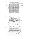
図1に、半導体装置の例として、ボトムゲート型のトランジスタ410の平面図および
断面図を示す。図1(A)は平面図であり、図1(B)および図1(C)は、図1(A)
におけるA−B断面およびC−D断面に係る断面図である。なお、図1(A)では、煩雑
になることを避けるため、トランジスタ410の構成要素の一部(例えば、酸化シリコン
膜407a、酸化アルミニウム膜407bなど)を省略している。FIG. 1 shows a plan view and a cross-sectional view of a
It is sectional drawing which concerns on the AB cross section and CD cross section in FIG. Note that in FIG. 1A, some components of the transistor 410 (eg, a
図1に示すトランジスタ410は、絶縁表面を有する基板400上に、ゲート電極層4
01、ゲート絶縁膜である酸化アルミニウム膜402aおよび酸化シリコン膜402b、
酸化物半導体層403、ソース電極層405a、ドレイン電極層405bおよび絶縁膜で
ある酸化シリコン膜407aおよび酸化アルミニウム膜407bを含む。A
01, an
It includes an
図1に示すトランジスタ410において、ゲート絶縁膜は、酸素を過剰に含む酸化アル
ミニウム膜402a(AlOx(x>3/2))と、酸素を過剰に含む酸化シリコン膜4
02b(SiOx(x>2))の積層である。酸化物半導体層403は、酸素添加処理が
行われており、酸素過剰領域を有する。酸素添加処理を行うことにより、酸化物半導体層
403に化学量論比より過剰に酸素を含有させることができるので、トランジスタ410
の信頼性が高められる。また、酸化アルミニウム膜402aは、当該酸素過剰領域からの
酸素脱離を抑制する効果を有する。In the
02b (SiOx (x> 2)). The
Reliability is improved. In addition, the
また、トランジスタ410は、酸素を過剰に含む酸化シリコン膜407a(SiOx(
x>2))と、酸素を過剰に含む酸化アルミニウム膜407b(AlOx(x>3/2)
)の積層を有する。酸化アルミニウムは、水分、酸素、その他の不純物を透過させにくい
というバリア機能を有しているため、デバイス完成後に水分等の不純物が外部より侵入す
るのを防ぐことができる。また、酸化物半導体層403より酸素が放出されるのを防ぐこ
とができる。この効果は、酸化アルミニウム膜402aおよび酸化アルミニウム膜407
bで酸化物半導体層403を挟み込むことでより顕著になる。なお、酸化シリコン膜40
7aは設けなくてもよい。The
x> 2)) and an
). Since aluminum oxide has a barrier function that hardly allows moisture, oxygen, and other impurities to pass therethrough, impurities such as moisture can be prevented from entering from the outside after the device is completed. In addition, release of oxygen from the
It becomes more prominent by sandwiching the
7a may not be provided.
また、ゲート絶縁膜もまた、酸素過剰領域を有するのが好ましい。ゲート絶縁膜が酸素
過剰領域を有していると、酸化物半導体層403からゲート絶縁膜への酸素の移動を防ぐ
ことができ、かつ、酸化シリコン膜402bから酸化物半導体層403への酸素の供給を
行うこともできるためである。The gate insulating film also preferably has an oxygen excess region. When the gate insulating film has an oxygen-excess region, oxygen can be prevented from moving from the
なお、トランジスタ410上には、さらに絶縁膜が設けられていても良い。また、ソー
ス電極層405aやドレイン電極層405bと配線とを電気的に接続させるために、酸化
シリコン膜407a、酸化アルミニウム膜407bなどには開口が形成されていても良い
。また、酸化物半導体層403の上方に、さらに、第2のゲート電極を有していても良い
。Note that an insulating film may be further provided over the
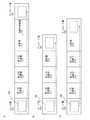
図2(A)乃至図2(D)にトランジスタ410の作製方法の一例を示す。 2A to 2D illustrate an example of a method for manufacturing the
まず、絶縁表面を有する基板400上に導電膜を形成した後、フォトリソグラフィ工程
によりゲート電極層401を形成する。なお、レジストマスクをインクジェット法で形成
してもよい。レジストマスクをインクジェット法で形成するとフォトマスクを使用しない
ため、製造コストを削減できる。First, after a conductive film is formed over the
絶縁表面を有する基板400に使用することができる基板に大きな制限はないが、少な
くとも、後の熱処理に耐えうる程度の耐熱性を有していることが必要となる。例えば、バ
リウムホウケイ酸ガラスやアルミノホウケイ酸ガラスなどのガラス基板、セラミック基板
、石英基板、サファイア基板などを用いることができる。また、シリコンや炭化シリコン
などの単結晶半導体基板、多結晶半導体基板、シリコンゲルマニウムなどの化合物半導体
基板、SOI基板などを適用することもでき、これらの基板上に半導体素子が設けられた
ものを基板400として用いてもよい。There is no particular limitation on a substrate that can be used as the
また、基板400として、可撓性基板を用いてもよい。可撓性基板を用いる場合、可撓
性基板上に酸化物半導体を含むトランジスタを直接形成してもよいし、他の基板に剥離層
を設けて剥離層の上にトランジスタ等を形成した後、形成したトランジスタを剥離層を用
いて剥離し、可撓性基板に転置してもよい。Further, a flexible substrate may be used as the
下地膜となる絶縁膜を基板400とゲート電極層401との間に設けてもよい。下地膜
は、基板400からの不純物元素の拡散を防止する機能があり、窒化シリコン膜、酸化シ
リコン膜、窒化酸化シリコン膜、または酸化窒化シリコン膜から選ばれた一または複数の
膜による積層構造により形成することができる。An insulating film serving as a base film may be provided between the
また、ゲート電極層401は、プラズマCVD法またはスパッタリング法等により、モ
リブデン、チタン、タンタル、タングステン、アルミニウム、銅、ネオジム、スカンジウ
ム等の金属材料またはこれらを主成分とする合金材料を用いて、単層でまたは積層して形
成することができる。The
次いで、ゲート電極層401上に酸化アルミニウム膜402aをプラズマCVD法また
はスパッタリング法等により形成する。続いて、酸化アルミニウム膜402a上に酸化シ
リコン膜402bをプラズマCVD法またはスパッタリング法等により形成する。さらに
、酸化シリコン膜402b上に酸化物半導体膜を形成し、フォトリソ工程などにより島状
に加工して酸化物半導体層403とする。酸化アルミニウム膜402aから酸化物半導体
膜の形成までは連続的に処理すると好ましい。また、酸化物半導体膜形成後、熱処理と酸
素添加処理を順に行うとより好ましい(図2(A)参照)。これにより、各膜中の水分や
水素の脱離と酸化物半導体層403への酸素添加を行うことができる。Next, an
また、成膜後の熱処理によって、膜質、酸化物半導体との界面特性が改質される絶縁膜
をゲート絶縁膜として用いても良い。いずれにしても、ゲート絶縁膜としての膜質が良好
であることは勿論のこと、酸化物半導体との界面準位密度を低減し、良好な界面を形成で
きるものであれば良い。Alternatively, an insulating film whose film quality and interface characteristics with an oxide semiconductor are modified by heat treatment after film formation may be used as the gate insulating film. In any case, any film can be used as long as it can reduce the interface state density with the oxide semiconductor and form a favorable interface as well as the quality of the gate insulating film.
なお、ゲート絶縁膜は酸素過剰領域を有すると、酸化物半導体層403の酸素欠損を補
填することが可能であるため好ましい。Note that it is preferable that the gate insulating film have an oxygen-excess region because oxygen vacancies in the
酸化物半導体層403は、膜厚2nm以上200nm以下、好ましくは5nm以上30
nm以下で形成する。酸化物半導体層403は、非単結晶または非晶質であって、以下で
示す酸化物を用いることができる。The
It is formed below nm. The
酸化物半導体には、In、Ga、ZnおよびSnから選ばれた2種以上を含む金属酸化
物材料を用いればよい。例えば、四元系金属酸化物であるIn−Sn−Ga−Zn−O系
の材料や、三元系金属酸化物であるIn−Ga−Zn−O系の材料、In−Sn−Zn−
O系の材料、In−Al−Zn−O系の材料、Sn−Ga−Zn−O系の材料、Al−G
a−Zn−O系の材料、Sn−Al−Zn−O系の材料や、二元系金属酸化物であるIn
−Zn−O系の材料、Sn−Zn−O系の材料、Al−Zn−O系の材料、Zn−Mg−
O系の材料、Sn−Mg−O系の材料、In−Mg−O系の材料、In−Ga−O系の材
料や、単元系金属酸化物であるIn−O系の材料、Sn−O系の材料、Zn−O系の材料
などを用いればよい。また、上記酸化物半導体にInとGaとSnとZn以外のもの、例
えばSiO2を含ませてもよい。For the oxide semiconductor, a metal oxide material containing two or more selected from In, Ga, Zn, and Sn may be used. For example, an In—Sn—Ga—Zn—O-based material that is a quaternary metal oxide, an In—Ga—Zn—O-based material that is a ternary metal oxide, In—Sn—Zn—,
O-based material, In-Al-Zn-O-based material, Sn-Ga-Zn-O-based material, Al-G
a-Zn-O-based material, Sn-Al-Zn-O-based material, and binary metal oxide In
-Zn-O-based material, Sn-Zn-O-based material, Al-Zn-O-based material, Zn-Mg-
O-based materials, Sn-Mg-O-based materials, In-Mg-O-based materials, In-Ga-O-based materials, In-O-based materials that are single metal oxides, Sn-O A Zn-O-based material or the like may be used. Further, the oxide semiconductor may contain a material other than In, Ga, Sn, and Zn, for example, SiO2 .
ここで、例えば、In−Ga−Zn−O系の酸化物半導体とは、インジウム(In)、
ガリウム(Ga)、亜鉛(Zn)を有する酸化物半導体、という意味であり、その組成比
は問わない。Here, for example, an In—Ga—Zn—O-based oxide semiconductor is indium (In),
It means an oxide semiconductor containing gallium (Ga) and zinc (Zn), and the composition ratio is not limited.
また、酸化物半導体には、化学式InMO3(ZnO)m(m>0)で表記される材料
を用いることができる。ここで、Mは、Zn、Ga、Al、MnおよびCoから選ばれた
一または複数の金属元素を示す。例えば、Mとして、Ga、GaおよびAl、Gaおよび
Mn、またはGaおよびCoなどがある。For the oxide semiconductor, a material represented by the chemical formula, InMO3 (ZnO)m (m> 0) can be used. Here, M represents one or more metal elements selected from Zn, Ga, Al, Mn, and Co. For example, M includes Ga, Ga and Al, Ga and Mn, or Ga and Co.
なお、酸化物半導体としてIn−Zn−O系の材料を用いる場合、用いるターゲットの
組成比は、原子数比で、In:Zn=50:1〜1:2(モル比に換算するとIn2O3
:ZnO=25:1〜1:4)、好ましくはIn:Zn=20:1〜1:1(モル比に換
算するとIn2O3:ZnO=10:1〜1:2)、さらに好ましくはIn:Zn=15
:1〜1.5:1(モル比に換算するとIn2O3:ZnO=15:2〜3:4)とする
。例えば、In−Zn−O系の酸化物半導体の形成に用いるターゲットは、原子数比がI
n:Zn:O=X:Y:Zのとき、Z>1.5X+Yとする。Note that in the case where an In—Zn—O-based material is used as the oxide semiconductor, the composition ratio of the target used is an atomic ratio, In: Zn = 50: 1 to 1: 2 (in2 O converted to a molar ratio).3
: ZnO = 25: 1 to 1: 4), preferably In: Zn = 20: 1 to 1: 1 (In2 O3 : ZnO = 10: 1 to 1: 2 in terms of molar ratio), more preferably In: Zn = 15
: 1 to 1.5: 1 (in terms of molar ratio, In2 O3 : ZnO = 15: 2 to 3: 4). For example, a target used for forming an In—Zn—O-based oxide semiconductor has an atomic ratio of I
When n: Zn: O = X: Y: Z, Z> 1.5X + Y.
また、酸化物半導体は、単結晶、多結晶(ポリクリスタルともいう。)または非晶質な
どの状態をとる。An oxide semiconductor is in a single crystal state, a polycrystalline (also referred to as polycrystal) state, an amorphous state, or the like.
好ましくは、酸化物半導体膜は、CAAC−OS(C Axis Aligned C
rystalline Oxide Semiconductor)膜とする。Preferably, the oxide semiconductor film is a CAAC-OS (C Axis Aligned C
a crystalline Oxide Semiconductor) film.
CAAC−OS膜は、完全な単結晶ではなく、完全な非晶質でもない。CAAC−OS
膜は、非晶質相に結晶部および非晶質部を有する結晶−非晶質混相構造の酸化物半導体膜
である。なお、当該結晶部は、一辺が100nm未満の立方体内に収まる大きさであるこ
とが多い。また、透過型顕微鏡(TEM:Transmission Electron
Microscope)による観察像では、CAAC−OS膜に含まれる非晶質部と結
晶部との境界は明確ではない。また、TEMによってCAAC−OS膜には粒界(グレイ
ンバウンダリーともいう。)は確認できない。そのため、CAAC−OS膜は、粒界に起
因する電子移動度の低下が抑制される。The CAAC-OS film is not completely single crystal nor completely amorphous. CAAC-OS
The film is an oxide semiconductor film having a crystal-amorphous mixed phase structure in which an amorphous phase includes a crystal part and an amorphous part. Note that the crystal part is often large enough to fit in a cube whose one side is less than 100 nm. In addition, a transmission microscope (TEM: Transmission Electron)
In the observation image by Microscope), the boundary between the amorphous part and the crystal part included in the CAAC-OS film is not clear. Further, a grain boundary (also referred to as a grain boundary) cannot be confirmed in the CAAC-OS film by TEM. Therefore, in the CAAC-OS film, reduction in electron mobility due to grain boundaries is suppressed.
CAAC−OS膜に含まれる結晶部は、c軸がCAAC−OS膜の被形成面の法線ベク
トルまたは表面の法線ベクトルに平行な方向に揃い、かつ、ab面に垂直な方向から見て
三角形状または六角形状の原子配列を有し、c軸に垂直な方向から見て金属原子が層状ま
たは金属原子と酸素原子とが層状に配列している。なお、異なる結晶部間で、それぞれa
軸およびb軸の向きが異なっていてもよい。本明細書において、単に垂直と記載する場合
、85°以上95°以下の範囲も含まれることとする。また、単に平行と記載する場合、
−5°以上5°以下の範囲も含まれることとする。The crystal part included in the CAAC-OS film has a c-axis aligned in a direction parallel to the normal vector of the formation surface of the CAAC-OS film or the normal vector of the surface, and is viewed from a direction perpendicular to the ab plane. It has a triangular or hexagonal atomic arrangement, and metal atoms are arranged in layers or metal atoms and oxygen atoms are arranged in layers as seen from the direction perpendicular to the c-axis. In addition, between different crystal parts, a
The directions of the axis and the b axis may be different. In this specification, a simple term “perpendicular” includes a range from 85 ° to 95 °. Also, when simply describing as parallel,
The range of −5 ° to 5 ° is also included.
なお、CAAC−OS膜において、結晶部の分布が一様でなくてもよい。例えば、CA
AC−OS膜の形成過程において、酸化物半導体膜の表面側から結晶成長させる場合、被
形成面の近傍に対し、表面の近傍では結晶部の占める割合が高くなることがある。また、
CAAC−OS膜へ不純物を添加することにより、当該不純物添加領域において結晶部が
非晶質化することもある。Note that the distribution of crystal parts in the CAAC-OS film is not necessarily uniform. For example, CA
In the formation process of the AC-OS film, in the case where crystal growth is performed from the surface side of the oxide semiconductor film, the ratio of crystal parts in the vicinity of the surface of the oxide semiconductor film may be higher in the vicinity of the surface. Also,
When an impurity is added to the CAAC-OS film, the crystal part in a region to which the impurity is added becomes amorphous in some cases.
CAAC−OS膜に含まれる結晶部のc軸は、CAAC−OS膜の被形成面の法線ベク
トルまたは表面の法線ベクトルに平行な方向に揃うため、CAAC−OS膜の形状(被形
成面の断面形状または表面の断面形状)によっては互いに異なる方向を向くことがある。
なお、結晶部のc軸の方向は、CAAC−OS膜が形成されたときの被形成面の法線ベク
トルまたは表面の法線ベクトルに平行な方向となる。結晶部は、成膜することにより、ま
たは成膜後に熱処理などの結晶化処理を行うことにより形成される。Since the c-axis of the crystal part included in the CAAC-OS film is aligned in a direction parallel to the normal vector of the formation surface of the CAAC-OS film or the normal vector of the surface, the shape of the CAAC-OS film (formation surface) Depending on the cross-sectional shape of the surface or the cross-sectional shape of the surface).
Note that the c-axis direction of the crystal part is parallel to the normal vector of the surface where the CAAC-OS film is formed or the normal vector of the surface. The crystal part is formed by film formation or by performing crystallization treatment such as heat treatment after film formation.
CAAC−OS膜を用いたトランジスタは、可視光や紫外光の照射による電気特性の変
動を低減することが可能である。よって、当該トランジスタは、信頼性が高い。A transistor including a CAAC-OS film can reduce variation in electrical characteristics due to irradiation with visible light or ultraviolet light. Therefore, the transistor has high reliability.
酸化物半導体膜は、スパッタリング法、分子線エピタキシー法、原子層堆積法またはパ
ルスレーザー蒸着法により形成する。ここでは、スパッタリング法により形成することが
できる。The oxide semiconductor film is formed by a sputtering method, a molecular beam epitaxy method, an atomic layer deposition method, or a pulsed laser deposition method. Here, it can be formed by a sputtering method.
酸化物半導体膜をCAAC−OS膜とする際には、基板400を加熱しながら酸化物半
導体膜を形成すればよく、基板400を加熱する温度としては、150℃以上450℃以
下とすればよく、好ましくは基板温度が200℃以上350℃以下とする。なお、酸化物
半導体膜の形成時に、基板を加熱する温度を高くすることで、非晶質な部分に対して結晶
部分の占める割合の多いCAAC−OS膜とすることができる。When the oxide semiconductor film is a CAAC-OS film, the oxide semiconductor film may be formed while the
スパッタリング法により酸化物半導体膜を形成する際、できる限り酸化物半導体膜に含
まれる水素濃度を低減させることが好ましい。水素濃度を低減させるには、スパッタリン
グ装置の処理室内に供給する雰囲気ガスとして、水素、水、水酸基または水素化物などの
不純物が除去された高純度の希ガス(代表的にはアルゴン)、酸素、および希ガスと酸素
との混合ガスを適宜用いる。このときの酸素分圧は高いほうが好ましく、雰囲気ガスを全
て酸素にしてもよい。さらには、該処理室の排気は、水の排気能力の高いクライオポンプ
または水素の排気能力の高いスパッタイオンポンプを用いればよい。When the oxide semiconductor film is formed by a sputtering method, it is preferable to reduce the concentration of hydrogen contained in the oxide semiconductor film as much as possible. In order to reduce the hydrogen concentration, as an atmosphere gas supplied into the processing chamber of the sputtering apparatus, a high-purity rare gas (typically argon) from which impurities such as hydrogen, water, a hydroxyl group, or a hydride are removed, oxygen, In addition, a mixed gas of a rare gas and oxygen is appropriately used. At this time, the oxygen partial pressure is preferably high, and the atmosphere gas may be all oxygen. Further, a cryopump having a high water exhaust capability or a sputter ion pump having a high hydrogen exhaust capability may be used for exhausting the processing chamber.
また、ゲート絶縁膜および酸化物半導体膜は、大気解放することなく連続的に形成する
。ゲート絶縁膜を形成する面またはゲート絶縁膜表面は、できるだけ平坦であることが好
ましい。これにより、酸化物半導体膜のCAAC−OS膜化を容易にできる。このような
面の平坦度は、算術平均粗さ(Ra)で1nm以下、好ましくは0.5nm以下とすれば
よい。例えば、基板400上に設けられたゲート電極層401の表面に付着した水素を含
む不純物を、熱処理またはプラズマ処理で除去した後、大気に解放することなくゲート絶
縁膜を形成し、続けて大気に解放することなく酸化物半導体膜を形成する。このようにす
ることで、ゲート電極層401の表面に付着した水素を含む不純物を低減し、また、ゲー
ト電極層401と酸化アルミニウム膜402aとの界面、および、酸化シリコン膜402
bと酸化物半導体膜との界面に、大気成分が付着することを抑制できる。その結果、電気
特性が良好で、信頼性の高いトランジスタ410を作製することができる。The gate insulating film and the oxide semiconductor film are formed continuously without being released to the atmosphere. The surface on which the gate insulating film is formed or the surface of the gate insulating film is preferably as flat as possible. Accordingly, the oxide semiconductor film can be easily formed into a CAAC-OS film. The flatness of such a surface may be an arithmetic average roughness (Ra) of 1 nm or less, preferably 0.5 nm or less. For example, after removing impurities including hydrogen attached to the surface of the
Atmospheric components can be prevented from adhering to the interface between b and the oxide semiconductor film. As a result, the
酸化物半導体膜を形成後、熱処理(第1の熱処理)を行うことが望ましい。この第1の
熱処理によって酸化物半導体膜中の、過剰な水素(水や水酸基を含む)を除去し、酸化物
半導体膜の構造を整え、エネルギーギャップ中の欠陥準位を低減することができる。第1
の熱処理の温度は、250℃以上700℃以下、好ましくは450℃以上600℃以下、
かつ、基板の歪み点未満とする。Heat treatment (first heat treatment) is preferably performed after the oxide semiconductor film is formed. By this first heat treatment, excess hydrogen (including water and hydroxyl groups) in the oxide semiconductor film can be removed, the structure of the oxide semiconductor film can be adjusted, and defect levels in the energy gap can be reduced. First
The temperature of the heat treatment is 250 ° C. or higher and 700 ° C. or lower, preferably 450 ° C. or higher and 600 ° C. or lower.
And, it should be less than the strain point of the substrate.
熱処理は、例えば、抵抗発熱体などを用いた電気炉に被処理物を導入し、窒素雰囲気下
、450℃、1時間の条件で行うことができる。この間、酸化物半導体膜は大気に触れさ
せず、水や水素の混入が生じないようにする。The heat treatment can be performed, for example, by introducing an object to be processed into an electric furnace using a resistance heating element and the like under a nitrogen atmosphere at 450 ° C. for 1 hour. During this time, the oxide semiconductor film is not exposed to the air so that water and hydrogen are not mixed.
熱処理装置は電気炉に限られず、加熱されたガスなどの媒体からの熱伝導、または熱輻
射によって、被処理物を加熱する装置を用いても良い。例えば、LRTA(Lamp R
apid Thermal Anneal)装置、GRTA(Gas Rapid Th
ermal Anneal)装置等のRTA(Rapid Thermal Annea
l)装置を用いることができる。LRTA装置は、ハロゲンランプ、メタルハライドラン
プ、キセノンアークランプ、カーボンアークランプ、高圧ナトリウムランプ、高圧水銀ラ
ンプなどのランプから発する光(電磁波)の輻射により、被処理物を加熱する装置である
。GRTA装置は、高温のガスを用いて熱処理を行う装置である。ガスとしては、アルゴ
ンなどの希ガス、または窒素のような、熱処理によって被処理物と反応しない不活性気体
が用いられる。The heat treatment apparatus is not limited to an electric furnace, and an apparatus for heating an object to be processed by heat conduction or heat radiation from a medium such as a heated gas may be used. For example, LRTA (Lamp R
API (Thermal Anneal) equipment, GRTA (Gas Rapid Th
RTA (Rapid Thermal Annea)
l) An apparatus can be used. The LRTA apparatus is an apparatus that heats an object to be processed by radiation of light (electromagnetic waves) emitted from a lamp such as a halogen lamp, a metal halide lamp, a xenon arc lamp, a carbon arc lamp, a high pressure sodium lamp, or a high pressure mercury lamp. The GRTA apparatus is an apparatus that performs heat treatment using a high-temperature gas. As the gas, an inert gas that does not react with an object to be processed by heat treatment, such as nitrogen or a rare gas such as argon, is used.
例えば、第1の熱処理として、熱せられた不活性ガス雰囲気中に被処理物を投入し、数
分間熱した後、当該不活性ガス雰囲気から被処理物を取り出すGRTA処理を行ってもよ
い。GRTA処理を用いると短時間での高温熱処理が可能となる。また、被処理物の耐熱
温度を超える温度条件であっても適用が可能となる。For example, as the first heat treatment, a GRTA process may be performed in which an object to be processed is put in a heated inert gas atmosphere and heated for several minutes, and then the object to be processed is extracted from the inert gas atmosphere. When GRTA treatment is used, high-temperature heat treatment can be performed in a short time. In addition, application is possible even under temperature conditions exceeding the heat resistance temperature of the object to be processed.
なお、不活性ガス雰囲気としては、窒素、または希ガス(ヘリウム、ネオン、アルゴン
等)を主成分とする雰囲気であって、水、水素などが含まれない雰囲気を適用するのが望
ましい。例えば、熱処理装置に導入する窒素や、ヘリウム、ネオン、アルゴン等の希ガス
の純度を、6N(99.9999%)以上、好ましくは7N(99.99999%)以上
(すなわち、不純物濃度が1ppm以下、好ましくは0.1ppm以下)とする。Note that as the inert gas atmosphere, an atmosphere containing nitrogen or a rare gas (such as helium, neon, or argon) as a main component and not including water, hydrogen, or the like is preferably used. For example, the purity of nitrogen or a rare gas such as helium, neon, or argon introduced into the heat treatment apparatus is 6N (99.9999%) or more, preferably 7N (99.99999%) or more (that is, the impurity concentration is 1 ppm or less). , Preferably 0.1 ppm or less).
ところで、上述の熱処理(第1の熱処理)には水素や水などを除去する効果があるから
、当該熱処理を、脱水化処理や、脱水素化処理などと呼ぶこともできる。このような脱水
化処理、脱水素化処理は、一回に限らず複数回行っても良い。なお、第1の熱処理中に、
不活性ガスを酸素を含むガスに切り替えても良い。酸素を含む雰囲気において第1の熱処
理を行うことで、酸素欠損に起因するエネルギーギャップ中の欠陥準位を低減することが
でき、酸化物半導体層をよりi型化または実質的にi型化にすることができる。By the way, since the above heat treatment (first heat treatment) has an effect of removing hydrogen, water, and the like, the heat treatment can be referred to as dehydration treatment, dehydrogenation treatment, or the like. Such dehydration treatment and dehydrogenation treatment are not limited to one time, and may be performed a plurality of times. During the first heat treatment,
The inert gas may be switched to a gas containing oxygen. By performing the first heat treatment in an atmosphere containing oxygen, defect states in the energy gap due to oxygen vacancies can be reduced, and the oxide semiconductor layer can be more i-type or substantially i-type. can do.
次に、酸化物半導体層403に酸素421の添加処理を行い、酸素過剰領域を形成する
(図2(A)参照)。酸素添加処理を行うことにより、酸素421を酸化物半導体膜に供
給して、酸化シリコン膜402b中、酸化シリコン膜402bと酸化物半導体層403と
の界面、酸化物半導体層403中、または酸化物半導体層403と後に形成する酸化シリ
コン膜407aとの界面の少なくとも一部に酸素過剰領域を形成する。酸化物半導体層4
03に酸素過剰領域を形成することで、酸素欠損を直ちに補填することができる。これに
よって、酸化物半導体層403中の電荷捕獲中心を低減することができる。Next,
By forming an oxygen excess region in 03, oxygen deficiency can be immediately compensated. Accordingly, charge trapping centers in the
酸素添加処理によって酸化物半導体層403の酸素の含有量を、酸化物半導体層403
の化学量論比を超える程度とする。例えば、当該酸素添加処理により酸化物半導体層40
3に添加される酸素の深さ方向の濃度のピークを1×10¹⁸/cm3以上3×1021
/cm3以下とするのが好ましい。添加される酸素421は、酸素ラジカル、酸素原子、
および/または酸素イオンを含む。なお、酸素過剰領域は、酸化物半導体層403の一部
(界面も含む)に存在していればよい。The oxygen content in the
The amount exceeds the stoichiometric ratio. For example, the oxide semiconductor layer 40 is formed by the oxygen addition treatment.
The concentration peak in the depth direction of oxygen added to 3 is 1 × 10¹⁸ / cm3 or more and 3 × 10²¹.
/ Cm3 or less is preferable. The added
And / or oxygen ions. Note that the oxygen-excess region only needs to exist in part (including the interface) of the
なお、酸化物半導体において、酸素は主たる成分材料の一つである。このため、酸化物
半導体中の酸素濃度を、SIMS(Secondary Ion Mass Spect
rometry)などの方法を用いて、正確に見積もることは難しい。つまり、酸化物半
導体に酸素が意図的に添加されたか否かを判別することは困難であるといえる。Note that oxygen is one of main component materials in an oxide semiconductor. Therefore, the oxygen concentration in the oxide semiconductor is changed to SIMS (Secondary Ion Mass Spec.
It is difficult to estimate accurately using a method such as (rometry). That is, it can be said that it is difficult to determine whether oxygen is intentionally added to the oxide semiconductor.
ところで、酸素には16Oの他に17Oや18Oといった同位体が存在し、自然界にお
ける17Oや18Oの存在比率はそれぞれ酸素原子全体の0.037%、0.204%程
度であることが知られている。つまり、酸化物半導体中におけるこれら同位体の濃度は、
SIMSなどの方法によって見積もることができる程度になるから、これらの濃度を測定
することで、酸化物半導体中の酸素濃度をより正確に見積もることが可能な場合がある。
よって、これらの濃度を測定することで、酸化物半導体に意図的に酸素が添加されたか否
かを判別しても良い。By the way, oxygen has isotopes such as17 O and18 O in addition to16 O, and the abundance ratios of17 O and18 O in nature are about 0.037% and 0.204% of the whole oxygen atom, respectively. It is known. In other words, the concentration of these isotopes in the oxide semiconductor is
Since it can be estimated by a method such as SIMS, it may be possible to more accurately estimate the oxygen concentration in the oxide semiconductor by measuring these concentrations.
Therefore, by measuring these concentrations, it may be determined whether oxygen is intentionally added to the oxide semiconductor.
また、酸化物半導体に添加される(含まれる)酸素421の一部は酸素の未結合手を酸
化物半導体中で有していてもよい。未結合手を有することにより、酸化物半導体中に残存
しうる水素と結合して、水素を固定化(非可動イオン化)することができるためである。In addition, part of the
添加される酸素(酸素ラジカル、酸素原子、および/または酸素イオン)は、酸素を含
むガスを用いてプラズマ発生装置により供給されてもよいし、またはオゾン発生装置によ
り供給されてもよい。より具体的には、例えば、半導体装置に対してエッチング処理を行
うための装置や、レジストマスクに対してアッシングを行うための装置などを用いて酸素
421を発生させ、酸化物半導体膜へ酸素添加処理を行うことができる。The added oxygen (oxygen radicals, oxygen atoms, and / or oxygen ions) may be supplied by a plasma generator using a gas containing oxygen, or may be supplied by an ozone generator. More specifically, for example,
また、イオンドーピング法やイオンインプランテーション法を用いて酸化物半導体膜、
該酸化物半導体膜側のゲート絶縁膜である酸化シリコン膜402bに酸素を添加してもよ
い。酸化物半導体膜に酸素過剰領域を形成することで、酸素欠損を直ちに補填することが
でき、また、酸化シリコン膜402bに酸素過剰領域を形成することで、後の加熱処理に
おいて酸化物半導体膜に酸素を供給することができる。なお、酸化シリコン膜402bに
接する酸化アルミニウム膜402aは、水分、酸素、その他の不純物を透過させにくいと
いうバリア機能を有しているため、酸化シリコン膜402bの過剰酸素を酸化物半導体膜
に供給することができる。In addition, an oxide semiconductor film using an ion doping method or an ion implantation method,
Oxygen may be added to the
次いで、ソース電極層およびドレイン電極層(これと同じ層で形成される配線を含む)
となる導電膜を形成し、これを加工してソース電極層405aおよびドレイン電極層40
5bとする(図2(B)参照)。Next, a source electrode layer and a drain electrode layer (including wiring formed in the same layer)
A conductive film to be formed is formed and processed to be a
5b (see FIG. 2B).
ソース電極層405aおよびドレイン電極層405bに用いる導電膜としては、後の熱
処理工程に耐えられる材料を用いる。例えば、Al、Cr、Cu、Ta、Ti、Mo、W
から選ばれた元素を含む金属膜、または上述した元素を成分とする金属窒化物膜(窒化チ
タン膜、窒化モリブデン膜、窒化タングステン膜)等を用いることができる。また、Al
、Cuなどの金属膜の下側または上側の一方または双方にTi、Mo、Wなどの高融点金
属膜またはそれらの金属窒化物膜(窒化チタン膜、窒化モリブデン膜、窒化タングステン
膜)を積層させた構成としても良い。また、ソース電極層、およびドレイン電極層に用い
る導電膜としては、導電性の金属酸化物で形成しても良い。導電性の金属酸化物としては
酸化インジウム(In2O3)、酸化スズ(SnO2)、酸化亜鉛(ZnO)、酸化イン
ジウム酸化スズ(In2O3−SnO2、ITOと略記する)、酸化インジウム酸化亜鉛
(In2O3−ZnO)またはこれらの金属酸化物材料に酸化シリコンを含ませたものを
用いることができる。As the conductive film used for the
A metal film containing an element selected from the above, or a metal nitride film (a titanium nitride film, a molybdenum nitride film, or a tungsten nitride film) containing the above-described element as a component can be used. Al
A refractory metal film such as Ti, Mo, or W or a metal nitride film thereof (titanium nitride film, molybdenum nitride film, tungsten nitride film) is laminated on one or both of the lower side or the upper side of a metal film such as Cu or Cu. It is good also as a composition. Alternatively, the conductive film used for the source electrode layer and the drain electrode layer may be formed using a conductive metal oxide. As the conductive metal oxide, indium oxide (In2 O3 ), tin oxide (SnO2 ), zinc oxide (ZnO), indium tin oxide (In2 O3 —SnO2 , abbreviated as ITO), oxidation Indium zinc oxide (In2 O3 —ZnO) or a metal oxide material containing silicon oxide can be used.
なお、導電膜のエッチングの際に、酸化物半導体層403がエッチングされ、分断する
ことのないようエッチング条件を最適化することが望まれる。しかしながら、導電膜のみ
をエッチングし、酸化物半導体層403を全くエッチングしないという条件を得ることは
難しく、溝部(凹部)を有する酸化物半導体層403となることもある。Note that it is preferable that etching conditions be optimized so that the
次いで、ソース電極層405aおよびドレイン電極層405bを覆い、酸化物半導体層
403の一部と接する絶縁膜を形成する。絶縁膜の形成前に、脱水や脱水素などを目的と
して酸化物半導体層403を、例えば、200℃以上450℃以下の温度で熱処理しても
よい。Next, an insulating film which covers the
絶縁膜は酸素を過剰に含む酸化シリコン膜407a(SiOx(x>2))と酸素を過
剰に含む酸化アルミニウム膜407b(AlOx(x>3/2))の積層である。酸化シ
リコン膜407aの厚さは、例えば、400nmとする。酸化アルミニウムは、水分、酸
素、その他の不純物を透過させにくいというバリア機能を有しているため、デバイス完成
後に水分等の不純物が外部より侵入するのを防ぐことができる。また、酸化物半導体層4
03より酸素が放出されるのを防ぐことができる。この効果は、酸化アルミニウム膜40
2aと酸化アルミニウム膜407bで酸化物半導体層403を挟み込むことでより顕著に
なる。なお、酸化シリコン膜407aは設けなくてもよい。The insulating film is a stack of a
Oxygen can be prevented from being released from 03. This effect is achieved by the aluminum oxide film 40.
2a and the
酸化シリコン膜407aおよび酸化アルミニウム膜407bは、それぞれ少なくとも1
nm以上の膜厚とし、スパッタ法など、当該膜に水、水素等の不純物を混入させない方法
を適宜用いて形成することができる。酸化シリコン膜407aおよび酸化アルミニウム膜
407bに水素が含まれると、その水素の酸化物半導体層403への侵入、または水素に
よる酸化物半導体層403中の酸素の引き抜き、が生じ酸化物半導体層403のバックチ
ャネルが低抵抗化(N型化)してしまい、寄生チャネルが形成されるおそれがある。よっ
て、酸化シリコン膜407aおよび酸化アルミニウム膜407bはできるだけ水素を含ま
ない膜になるように、形成時に水素を用いないことが重要である。Each of the
The film can be formed to a thickness of nm or more by appropriately using a method such as sputtering, in which impurities such as water and hydrogen are not mixed into the film. When hydrogen is contained in the
酸化シリコン膜407aおよび酸化アルミニウム膜407bを形成する際に用いるスパ
ッタガスは水素、水、水酸基または水素化物などの不純物が除去された高純度ガスを用い
ることが好ましい。A sputtering gas used for forming the
その後、熱処理(第2の熱処理)を行う。該熱処理の温度は、好ましくは200℃以上
650℃以下、より好ましくは450℃以上650℃以下または基板の歪み点未満、より
好ましくは275℃以上325℃以下とする。該熱処理は、窒素、酸素、超乾燥空気(水
の含有量が20ppm以下、好ましくは1ppm以下、より好ましくは10ppb以下の
空気)、または希ガス(アルゴン、ヘリウムなど)の雰囲気下で行えばよいが、上記窒素
、酸素、超乾燥空気、または希ガス等の雰囲気に水、水素などが含まれないことが好まし
い。また、加熱処理装置に導入する窒素、酸素、または希ガスの純度を、6N(99.9
999%)以上好ましくは7N(99.99999%)以上(即ち不純物濃度を1ppm
以下、好ましくは0.1ppm以下)とすることが好ましい。Thereafter, heat treatment (second heat treatment) is performed. The temperature of the heat treatment is preferably 200 ° C. or higher and 650 ° C. or lower, more preferably 450 ° C. or higher and 650 ° C. or lower, or less than the strain point of the substrate, more preferably 275 ° C. or higher and 325 ° C. or lower. The heat treatment may be performed in an atmosphere of nitrogen, oxygen, ultra-dry air (air with a water content of 20 ppm or less, preferably 1 ppm or less, more preferably 10 ppb or less), or a rare gas (such as argon or helium). However, it is preferable that water, hydrogen, and the like are not contained in the atmosphere of nitrogen, oxygen, ultra-dry air, or a rare gas. Further, the purity of nitrogen, oxygen, or a rare gas introduced into the heat treatment apparatus is set to 6N (99.9).
999%) or more, preferably 7N (99.99999%) or more (that is, the impurity concentration is 1 ppm)
Or less, preferably 0.1 ppm or less).
以上の工程で、酸素欠損の形成を抑制した酸化物半導体層403を形成することができ
る。なお、第2の熱処理によって、酸化物半導体を構成する主成分材料の一つである酸素
を、酸素を含有する絶縁膜である酸化シリコン膜402b、酸化シリコン膜407aより
酸化物半導体層403へ供給してもよい。また、酸化物半導体層403をCAAC−OS
膜とした場合、酸素添加処理によって酸化物半導体層403中に含まれる結晶構造が乱さ
れて非晶質化することがあるが、酸素添加処理後に熱処理を行うことによって、再度、結
晶化することが可能である。Through the above steps, the
In the case of a film, the crystal structure included in the
なお、熱処理(第2の熱処理)のタイミングは、本実施の形態の構成に限定されないが
、該熱処理は、少なくとも酸化アルミニウム膜407bの形成後に行う必要がある。酸化
アルミニウム膜は、水素、水分などの不純物、および酸素の両方に対して膜を透過させな
い遮断効果(ブロック効果)が高く、酸化アルミニウム膜407bの形成後に熱処理を行
うことで、酸化物半導体層403からの酸素の放出を防止することができるためである。Note that the timing of the heat treatment (second heat treatment) is not limited to the structure in this embodiment, but the heat treatment needs to be performed at least after the
上述のように、第1の熱処理と第2の熱処理の少なくとも一方を適用することで、酸化
物半導体層403を、その主成分以外の不純物が極力含まれないように高純度化すること
ができる。高純度化された酸化物半導体層403中にはドナーに由来するキャリアが極め
て少なく(ゼロに近い)、キャリア濃度は1×10¹⁴/cm3未満、好ましくは1×1
012/cm3未満、さらに好ましくは1×1011/cm3未満である。As described above, by applying at least one of the first heat treatment and the second heat treatment, the
It is less than 012 / cm3 , more preferably less than 1 × 10¹¹ / cm3 .
以上の工程でトランジスタ410が形成される(図2(D)参照)。トランジスタ41
0は、酸素添加処理によって酸素過剰領域を作製することで、酸化物半導体層403中ま
たは界面における酸素欠損の形成を抑制し、酸素欠損に起因するエネルギーギャップ中の
ドナー準位を低減する、または実質的になくすことができる。また、酸素添加処理、また
はその後の熱処理によって、酸化物半導体層403へと酸素を供給することで、酸化物半
導体層403の酸素欠損を補填することができる。また、該供給された酸素によって、酸
化物半導体層403中に残留する水素イオンを固定化しうる。よって、トランジスタ41
0は、電気的特性変動が抑制されており、電気的に安定である。Through the above steps, the
0 suppresses formation of oxygen vacancies in the
0 is electrically stable because fluctuations in the electrical characteristics are suppressed.
また、トランジスタ410は、脱水化または脱水素化を目的とする熱処理を行うことが
好ましく、該熱処理によって、水素、水、水酸基または水素化物(水素化合物ともいう)
などの不純物を酸化物半導体膜より意図的に排除し、高純度化し、i型(真性)化された
酸化物半導体層403を含むトランジスタとすることができる。高純度化された酸化物半
導体層403中にはキャリアが極めて少ない(ゼロに近い)。The
Thus, a transistor including the
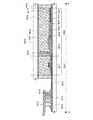
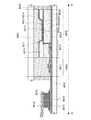
図3に、本実施の形態に係るトランジスタの別の構成例を示す。図3(A)はトランジ
スタ420の平面図であり、図3(B)および図3(C)は、図3(A)におけるE−F
断面およびG−H断面に係る断面図である。なお、図3(A)では、煩雑になることを避
けるため、トランジスタ420の構成要素の一部(例えば、酸化シリコン膜407a、酸
化アルミニウム膜407bなど)を省略している。FIG. 3 illustrates another configuration example of the transistor according to this embodiment. FIG. 3A is a plan view of the
It is sectional drawing which concerns on a cross section and GH cross section. Note that in FIG. 3A, some components of the transistor 420 (eg, a
図3に示すトランジスタ420は、図1に示すトランジスタ410と同様に、絶縁表面
を有する基板400上に、ゲート電極層401、ゲート絶縁膜である酸化アルミニウム膜
402aおよび酸化シリコン膜402b、酸化物半導体層403、ソース電極層405a
、ドレイン電極層405bおよび絶縁膜である酸化シリコン膜407aおよび酸化アルミ
ニウム膜407bを含む。A
, A
図3に示すトランジスタ420と図1に示すトランジスタ410との相違の一は、ゲー
ト電極層401の上に、ゲート電極層401aを有することである。ゲート電極層401
aの形成方法および材料等は、ゲート電極層401を参酌することができる。One difference between the
The
なお、ゲート電極層とゲート絶縁膜との間に、ゲート絶縁膜に接する材料層として、窒
素を含むIn−Ga−Zn−O膜や、窒素を含むIn−Sn−O膜や、窒素を含むIn−
Ga−O膜や、窒素を含むIn−Zn−O膜や、窒素を含むSn−O膜や、窒素を含むI
n−O膜や、金属窒化膜(InN、ZnNなど)を設けることが好ましい。これらの膜は
5eV、好ましくは5.5eV以上の仕事関数を有し、トランジスタの電気特性のしきい
値電圧をプラスにすることができ、所謂ノーマリーオフのスイッチング素子を実現できる
。例えば、窒素を含むIn−Ga−Zn−O膜を用いる場合、少なくとも酸化物半導体層
403より高い窒素濃度、具体的には7原子%以上の窒素を含むIn−Ga−Zn−O膜
を用いる。その他の詳細については、トランジスタ410についての説明を参酌すること
ができる。Note that as a material layer in contact with the gate insulating film between the gate electrode layer and the gate insulating film, an In—Ga—Zn—O film containing nitrogen, an In—Sn—O film containing nitrogen, or nitrogen is contained. In-
Ga—O film, In—Zn—O film containing nitrogen, Sn—O film containing nitrogen, I containing nitrogen
It is preferable to provide an n-O film or a metal nitride film (InN, ZnN, or the like). These films have a work function of 5 eV, preferably 5.5 eV or more, can increase the threshold voltage of the electrical characteristics of the transistor, and can realize a so-called normally-off switching element. For example, in the case of using an In—Ga—Zn—O film containing nitrogen, at least a nitrogen concentration higher than that of the
図3に示す構成を採用した場合にも、図1に示す構成を採用した場合と同様の効果を得
ることができる。Even when the configuration shown in FIG. 3 is adopted, the same effect as that obtained when the configuration shown in FIG. 1 is adopted can be obtained.
本実施の形態で示すトランジスタは、酸素添加処理によって酸化物半導体層の酸素の含
有量を増やし、酸素欠損を減少させることで、電気的バイアスストレスや熱ストレスに起
因する劣化を抑制し、光による劣化を低減することができる。また、酸素添加処理によっ
て、酸化物半導体層に隣接するゲート絶縁層に酸素過剰領域を形成することによって、酸
化物半導体層中の酸素欠損を補填することが可能である。さらに、酸素を過剰に含んだ酸
化アルミニウム膜により、酸化物半導体層を挟み込むことにより、酸素の減少を顕著に抑
えることが可能となる。また、先に言及した熱処理は、水素、水、水酸基または水素化物
(水素化合物ともいう)などの水素原子を含む不純物を酸化物半導体より排除するため、
高純度化およびi型(真性)化された酸化物半導体層を得ることができ、しきい値電圧な
どの電気的特性変動が抑制され、電気的に安定なトランジスタとすることができる。In the transistor described in this embodiment, the oxygen content in the oxide semiconductor layer is increased by oxygen addition treatment and oxygen vacancies are reduced, so that deterioration due to electrical bias stress or thermal stress is suppressed and light is emitted. Deterioration can be reduced. In addition, oxygen vacancies in the oxide semiconductor layer can be filled by forming an oxygen-excess region in the gate insulating layer adjacent to the oxide semiconductor layer by an oxygen addition treatment. Furthermore, by sandwiching the oxide semiconductor layer with an aluminum oxide film containing excess oxygen, reduction in oxygen can be significantly suppressed. In addition, the heat treatment described above excludes impurities including hydrogen atoms such as hydrogen, water, a hydroxyl group, or hydride (also referred to as a hydrogen compound) from an oxide semiconductor.
A highly purified and i-type (intrinsic) oxide semiconductor layer can be obtained, and variation in electrical characteristics such as threshold voltage can be suppressed, whereby an electrically stable transistor can be obtained.
以上示したように、本実施の形態によって安定した電気的特性を有する酸化物半導体を
用いた半導体装置を提供することができる。また、信頼性の高い半導体装置を提供するこ
とができる。As described above, according to this embodiment, a semiconductor device including an oxide semiconductor having stable electrical characteristics can be provided. In addition, a highly reliable semiconductor device can be provided.
以上、本実施の形態に示す構成、方法などは、他の実施の形態に示す構成、方法などと
適宜組み合わせて用いることができる。The structures, methods, and the like described in this embodiment can be combined as appropriate with any of the structures, methods, and the like described in the other embodiments.
(実施の形態2)
本実施の形態では、実施の形態1に示した半導体装置の酸化物半導体層等を形成する成
膜装置の一例について、図4乃至図6を用いて説明する。なお、実施の形態1と同一部分
または同様な機能を有する部分、および工程は、実施の形態1と同様に行うことができ、
繰り返しの説明は省略する。また、同じ箇所の詳細な説明は省略する。(Embodiment 2)
In this embodiment, an example of a deposition apparatus for forming the oxide semiconductor layer or the like of the semiconductor device described in
The repeated explanation is omitted. Detailed descriptions of the same parts are omitted.
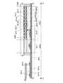
図4(A)は、本実施の形態で説明する成膜装置の構成を説明するブロック図である。 FIG. 4A is a block diagram illustrating a structure of a film formation apparatus described in this embodiment.
成膜装置は、ロード室101、第1の成膜室111、第2の成膜室112、第3の成膜
室113、加熱室114、加酸素化処理室115、およびアンロード室102が順に接続
される。なお、今後、ロード室101、アンロード室102を除く各部屋について、それ
ぞれを区別して説明する必要のないときは総称して処理室と呼ぶこともある。当該成膜装
置は搬送ロボットを有さず、ベルトコンベアのように順次各処理室に基板を搬送するもの
で、インライン装置とも呼称される。The film formation apparatus includes a load chamber 101, a first
ロード室101に搬入された基板100は、移動手段によって、第1の成膜室111、
第2の成膜室112、と順次、加酸素化処理室115まで送られたのち、アンロード室1
02に搬送される。各処理室では、必ずしも処理を行う必要はなく、工程を省きたい場合
は適宜、処理をせずに次の処理室に基板を搬送することもできる。The
After being sequentially sent to the second
It is conveyed to 02. In each processing chamber, it is not always necessary to perform processing, and if it is desired to omit a process, the substrate can be transferred to the next processing chamber without performing processing as appropriate.
ロード室101は、装置外から成膜装置に基板の搬入を行う機能を有する。例えば、ロ
ード室101は、水平な状態の基板100を水平面に対して立てる機構を有していてもよ
い。The load chamber 101 has a function of carrying a substrate into the film formation apparatus from outside the apparatus. For example, the load chamber 101 may have a mechanism that stands the
一例として、アンロード室102は、ロード室101とは逆に、立てた状態の基板10
0を水平の状態に寝かせる機構を有していてもよい。処理を終え、移動手段によってアン
ロード室102に搬入された基板100は、アンロード室102にて立てた状態から水平
方向な状態とされ、その後、装置外へ基板100が搬出される。勿論、基板100を立て
たままロード室101に基板100を搬入してもよいし、基板100を水平のまま各処理
室で処理を行ってもよい。As an example, the unload chamber 102 is opposed to the load chamber 101, and the
You may have the mechanism which puts 0 to a horizontal state. After the processing, the
基板100を各処理室において立てる場合には、基板100は、ロード室101から、
各処理室で処理を終えてアンロード室102に搬出されるまでの間、基板100の成膜面
と鉛直方向との成す角が1°以上、30°以内、好ましくは5°以上15°以内に収まる
ように保持される。このように、基板100を鉛直方向から僅かに傾けることにより、装
置の床面積、所謂フットプリントを小さくすることができ、基板サイズが、例えば、第1
1世代、第12世代などへ大型化すればするほどクリーンルーム等の設計の容易さやコス
トの面においても有効である。さらに、基板100を鉛直方向から僅かだけ傾けることに
より、基板100に付着するごみ、パーティクルを低減できるため好ましい。When the
The angle formed by the film formation surface of the
The larger the size is to the first generation, the twelfth generation, etc., the more effective the design and cost of a clean room or the like. Furthermore, it is preferable to tilt the
ロード室101、およびアンロード室102のそれぞれは、室内を真空にする排気手段
と、真空状態から大気圧する際に用いるガス導入手段とを有する。ガス導入手段から導入
されるガスは、空気、若しくは窒素や希ガスなどの不活性ガスなどを適宜用いればよい。Each of the load chamber 101 and the unload chamber 102 includes an exhaust unit that evacuates the chamber, and a gas introduction unit that is used when the atmospheric pressure is reached from the vacuum state. As the gas introduced from the gas introduction means, air or an inert gas such as nitrogen or a rare gas may be used as appropriate.
また、ロード室101は、基板100を予備加熱するための加熱手段を有していても良
い。排気動作と並行して基板100に対して予備加熱を行うことで、基板100に吸着す
るガス等の不純物(水、水酸基などを含む)を脱離させることができるため好ましい。排
気手段としては、例えば、クライオポンプ、イオンポンプ、チタンサブリメーションポン
プなどの吸着型の真空ポンプ、或いは、ターボ分子ポンプにコールドトラップを加えたも
のを用いると良い。In addition, the load chamber 101 may have a heating unit for preheating the
ロード室101、アンロード室102、およびそれぞれの処理室は、ゲートバルブを介
して連結されている。したがって、基板100が処理を終えて次の処理室へ移る際には、
ゲートバルブを開けて基板100が搬入される。なお、このゲートバルブは、処理室間に
おいて必要でなければ設けなくても良い。また、それぞれの処理室には、排気手段、圧力
調整手段、ガス導入手段などを有し、処理していない状態であっても常に減圧清浄な状態
に保つことができる。ゲートバルブによって各処理室が隔離されることにより、他の処理
室からの汚染を抑制することができる。The load chamber 101, the unload chamber 102, and the respective processing chambers are connected via a gate valve. Therefore, when the
The gate valve is opened and the
また、成膜装置の各室は必ずしも一直線上に配置する必要はなく、例えば、途中で折っ
たり、曲げたりしてもよいし、必要であれば分岐しても構わない。Further, the chambers of the film forming apparatus are not necessarily arranged on a straight line. For example, the chambers may be folded or bent in the middle, or may be branched if necessary.
次に、第1の成膜室111、第2の成膜室112、および第3の成膜室113において
、これらに共通する構成について説明する。また、その後、加熱室114および加酸素化
処理室115についても同様に、これらに共通する部分について説明する。最後に、それ
ぞれの処理室における特徴についての説明を行う。Next, a configuration common to the first
第1乃至第3までの成膜室はスパッタリング装置またはCVD装置が配置される。 A sputtering apparatus or a CVD apparatus is disposed in the first to third film formation chambers.
上記成膜室で用いるスパッタリング装置には、例えば、マイクロ波スパッタリング法、
RFプラズマスパッタリング法、ACスパッタリング法、もしくはDCスパッタリング法
などのスパッタリング装置を用いることができる。Examples of the sputtering apparatus used in the film formation chamber include a microwave sputtering method,
A sputtering apparatus such as an RF plasma sputtering method, an AC sputtering method, or a DC sputtering method can be used.
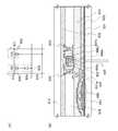
ここで、DCスパッタリング法を適用した成膜室の一例について図5を用いて説明する
。DCスパッタリング法を適用した成膜室154について、図5(A)に基板100の進
行方向に対して垂直方向の断面模式図を、また、図5(B)に、進行方向に対して平行且
つ水平な断面の断面模式図を示す。Here, an example of a film formation chamber to which the DC sputtering method is applied is described with reference to FIGS. With respect to the
まず、基板100は、成膜面と鉛直方向との成す角が少なくとも1°以上30°以内、
好ましくは5°以上15°以内に収まるように、基板支持部141によって固定されてい
る。基板支持部141は移動手段143に固定されている。移動手段143は、処理中に
基板100が動かないよう、基板支持部141を固定しておくだけでなく、基板100を
図5(B)中の破線に沿った方向(矢印に示す方向)に移動可能であり、ロード室101
、アンロード室102、および各処理室において、基板100の搬入出を行う機能も有す
る。First, the
Preferably, it is fixed by the
The unload chamber 102 and each processing chamber also have a function of loading and unloading the
成膜室154には、ターゲット151および、防着板153が基板100に平行になる
ように配置される。ターゲット151と基板100とを平行に配置することにより、ター
ゲットとの距離が異なることに起因するスパッタ膜の膜厚や、スパッタ膜の段差に対する
カバレッジなどのばらつきなどをなくすことができる。In the
また、成膜室154は、基板支持部141の背面に位置するように、基板加熱手段15
5を有していても良い。基板加熱手段155により、基板100を加熱しながら成膜処理
を施すことができる。基板加熱手段155としては、例えば、抵抗加熱ヒータや、ランプ
ヒータなどを用いることができる。なお、基板加熱手段155は必要でなければなくすこ
ともできる。In addition, the
5 may be included. The substrate heating means 155 can perform film formation while heating the
成膜室154は、圧力調整手段157を有し、成膜室154内を所望の圧力に減圧する
ことができる。圧力調整手段に用いる排気装置としては、例えば、クライオポンプ、イオ
ンポンプ、チタンサブリメーションポンプなどの吸着型の真空ポンプ、或いは、ターボ分
子ポンプにコールドトラップを加えたものを用いると良い。The
また、成膜室154は成膜ガス等を導入するためのガス導入手段159を有する。例え
ば、希ガスを主成分としたガスに酸素を添加したガスを導入して反応性スパッタリング法
による成膜を行うことにより、酸化膜を形成することができる。さらに、ガス導入手段1
59から導入されるガスは、水素や水、水酸化物などの不純物が低減された高純度ガスを
導入することができる。例えば、酸素、窒素、希ガス(代表的にはアルゴン)、またはこ
れらの混合ガスを導入することができる。The
As the gas introduced from 59, a high-purity gas in which impurities such as hydrogen, water, and hydroxide are reduced can be introduced. For example, oxygen, nitrogen, a rare gas (typically argon), or a mixed gas thereof can be introduced.
以上のような圧力調整手段157とガス導入手段159を有する成膜室154では、水
素分子や水(H2O)などの水素を含む化合物などが(より好ましくは炭素原子を含む化
合物と共に)除去されるため、当該成膜室で成膜した膜中に含まれる不純物の濃度を低減
できる。In the
成膜室154と隣接する部屋との境界は、ゲートバルブ161で仕切られている。ゲー
トバルブ161で室内を隔離することにより、室内の不純物を排気しやすくし、成膜雰囲
気を清浄に保つことができる。さらに、室内を清浄な状態にした後にゲートバルブ161
を開放し、基板100を搬出することにより、隣接する処理室への汚染を抑制することが
できる。なお、必要でなければ、ゲートバルブ161をなくすことができる。The boundary between the
By opening and removing the
なお、成膜室154は、図5(C)に示すように、基板100を図中に示す破線の方向
に沿って矢印の方向にスライドさせながら成膜する構成としてもよい。この様な構成とす
ることにより、ターゲットのサイズを小さくできるため、基板の大型化に対し、ターゲッ
トのサイズを基板と同程度まで大きくできない場合などには好適である。Note that as illustrated in FIG. 5C, the
加熱室114は、基板100に対して熱処理を行うことができる。 The
加熱装置には、抵抗加熱ヒータ、ランプ、または加熱されたガスを用いるものなどを設
けると良い。The heating device may be provided with a resistance heater, a lamp, or a device using heated gas.
図6(A)および図6(B)に棒状のヒータを用いた加熱装置を適用した、加熱室の一
例を示す。図6(A)は、基板の移動方向に対して垂直な断面に相当する、加熱室170
の断面模式図であり、図6(B)は、基板の移動方向に水平な断面に相当する断面模式図
である。6A and 6B illustrate an example of a heating chamber to which a heating device using a rod-shaped heater is applied. FIG. 6A illustrates a
FIG. 6B is a schematic cross-sectional view corresponding to a horizontal cross section in the moving direction of the substrate.
加熱室170には成膜室154と同様、移動手段143によって基板支持部141に支
持された基板100を搬入、搬出することができる。Similarly to the
加熱室170には棒状のヒータ171が基板100と平行になるように配置されている
。図6(A)には、その断面となる形状を模式的に現している。棒状のヒータ171には
、抵抗加熱ヒータ、またはランプヒータを用いることができる。抵抗加熱ヒータには、誘
導加熱を用いたものも含まれる。また、ランプは中心波長が赤外線領域にあるものが好ま
しい。棒状のヒータ171を基板100に平行に配置することにより、これらの距離を一
定にし、均一に加熱することができる。また、棒状のヒータ171はそれぞれ個別に温度
を制御できることが好ましい。例えば、上部のヒータよりも下部のヒータを高い温度に設
定することにより、基板100を均一な温度で加熱することができる。なお、本実施の形
態では、棒状のヒータを用いる構成としたが、ヒータの構成はこれに限定されず、面状(
板状)のヒータでも良いし、これらヒータを動かしながら熱処理を行うこともできる。ま
た、レーザを用いた加熱方法を用いてもよい。A rod-shaped
A plate-shaped heater may be used, and heat treatment may be performed while moving these heaters. Further, a heating method using a laser may be used.
また、加熱室170は、棒状のヒータ171と基板100の間に、保護板173を設け
る構成としている。保護板173は棒状のヒータ171、および基板100の保護のため
に設けられるもので、例えば、石英などを用いることができる。保護板173は必要なけ
れば設けなくてもよい。なお、本構成では棒状のヒータ171と基板100との間にシャ
ッターを有さない構成としているため、基板全面を均一に加熱することができる。In addition, the
また、加熱室170は、成膜室154と同様の圧力調整手段157およびガス導入手段
159を有する。したがって、熱処理中や処理を行っていない状態においても常に減圧清
浄な状態を保持することができる。また、加熱室170内の水素分子や水(H2O)など
の水素を含む化合物などが(より好ましくは炭素原子を含む化合物と共に)除去されるた
め、当該加熱室で処理した膜中、膜界面、膜表面に含有、もしくは吸着する不純物の濃度
を低減できる。The
また、圧力調整手段157およびガス導入手段159により、不活性ガス雰囲気や、酸
素を含む雰囲気での熱処理が可能である。このような機構は、加酸素化処理室115にも
付いており、当該処理室にて加酸素化処理が可能となっている。具体的には室内を、酸素
をプラズマ化した雰囲気とするプラズマドープや、イオンドーピング法を用いるなどして
行う。なお、不活性ガス雰囲気としては、窒素、または希ガス(ヘリウム、ネオン、アル
ゴン等)を主成分とする雰囲気であって、水、水素などが含まれない雰囲気を適用するの
が望ましい。例えば、加熱室170に導入する窒素や、ヘリウム、ネオン、アルゴン等の
希ガスの純度を、6N(99.9999%)以上、好ましくは7N(99.99999%
)以上(すなわち、不純物濃度が1ppm以下、好ましくは0.1ppm以下)とする。Further, the pressure adjusting means 157 and the gas introducing means 159 can perform heat treatment in an inert gas atmosphere or an atmosphere containing oxygen. Such a mechanism is also provided in the oxygenation treatment chamber 115, and the oxygenation treatment can be performed in the treatment chamber. Specifically, the inside of the chamber is performed by plasma doping using an atmosphere in which oxygen is turned into plasma or ion doping. Note that as the inert gas atmosphere, an atmosphere containing nitrogen or a rare gas (such as helium, neon, or argon) as a main component and not including water, hydrogen, or the like is preferably used. For example, the purity of nitrogen or a rare gas such as helium, neon, or argon introduced into the
) Or more (that is, the impurity concentration is 1 ppm or less, preferably 0.1 ppm or less).
続いて、各処理室における個別の特徴、構成について説明を行う。 Subsequently, individual features and configurations in each processing chamber will be described.
第1の成膜室111では基板100上に酸化アルミニウム膜402aを形成する。成膜
装置には、例えば、スパッタリング装置を適用する。続いて、第2の成膜室112では酸
化シリコン膜402bを形成する。成膜装置には、例えば、スパッタリング装置を適用す
る。さらに続けて、第3の成膜室113では酸化物半導体層403を形成する。成膜装置
には、例えば、スパッタリング装置を適用する。成膜方法としては、マイクロ波プラズマ
スパッタリング法、RFプラズマスパッタリング法、ACスパッタリング法、もしくはD
Cスパッタリング法を適用することができる。In the first
C sputtering method can be applied.
次に加熱室114では基板加熱手段155により、基板100の軟化点未満の温度で基
板100を加熱することができる。Next, in the
加熱室114では、例えば200℃以上700℃以下の温度で基板100を加熱する。
さらに圧力調整手段157およびガス導入手段159によって、熱処理中の雰囲気を、例
えば、10Pa乃至1気圧(1013.25hPa)とし、酸素雰囲気下、窒素雰囲気下
、または酸素と窒素の混合雰囲気下で熱処理を行うことができる。In the
Further, the atmosphere during the heat treatment is set to, for example, 10 Pa to 1 atm (1013.25 hPa) by the
最後に、加酸素化処理室115では、酸素雰囲気下において加酸素化処理を行うことが
できる。なお、圧力調整手段157およびガス導入手段159によって、当該加酸素化処
理は酸素と他の元素を含む混合雰囲気下で行うことができる。Finally, in the oxygenation treatment chamber 115, oxygenation treatment can be performed in an oxygen atmosphere. Note that the oxygenation treatment can be performed in a mixed atmosphere containing oxygen and other elements by the
つぎに、図4(B)に示すブロック図に沿って、他の成膜装置について説明する。 Next, another film formation apparatus will be described with reference to a block diagram shown in FIG.
まず、各処理室における個別の特徴、構成について説明を行う。ロード室201、アン
ロード室202については、図4(A)に示したものと同様のものであるため説明は省く
。First, individual features and configurations in each processing chamber will be described. The
第1の成膜室211では酸化シリコン膜407aを形成する。成膜装置には、例えば、
スパッタリング装置を適用する。続いて、第2の成膜室212では酸化アルミニウム膜4
07bを形成する。成膜装置には、例えば、スパッタリング装置を適用する。成膜方法と
しては、マイクロ波プラズマスパッタリング法、RFプラズマスパッタリング法、ACス
パッタリング法、もしくはDCスパッタリング法を適用することができる。なお、酸化シ
リコン膜407aは形成しなくてもよい。In the first deposition chamber 211, a
A sputtering apparatus is applied. Subsequently, the aluminum oxide film 4 is formed in the second film formation chamber 212.
07b is formed. For example, a sputtering apparatus is applied to the film forming apparatus. As a film formation method, a microwave plasma sputtering method, an RF plasma sputtering method, an AC sputtering method, or a DC sputtering method can be applied. Note that the
次に加熱室213では基板加熱手段155により、基板100の軟化点未満の温度で基
板100を加熱することができる。Next, in the heating chamber 213, the
加熱室213では、例えば、275℃以上325℃以下の温度で基板100を加熱する
。さらに圧力調整手段157およびガス導入手段159によって、熱処理中の雰囲気を、
例えば、10Pa乃至1気圧(1013.25hPa)とし、酸素雰囲気下、窒素雰囲気
下、または酸素と窒素の混合雰囲気下で熱処理を行うことができる。In the heating chamber 213, for example, the
For example, heat treatment can be performed at 10 Pa to 1 atm (1013.25 hPa) in an oxygen atmosphere, a nitrogen atmosphere, or a mixed atmosphere of oxygen and nitrogen.
図4(B)に示した成膜装置は、他の成膜装置に置き換えることも可能である。一例と
して、図4(C)に示すブロック図に沿って、当該成膜装置について説明する。The film formation apparatus illustrated in FIG. 4B can be replaced with another film formation apparatus. As an example, the film formation apparatus will be described with reference to a block diagram of FIG.
まず、各処理室における個別の特徴、構成について説明を行う。ロード室301、アン
ロード室302については、図4(A)に示したものと同様のものであるため説明は省く
。First, individual features and configurations in each processing chamber will be described. The
第1の成膜室311では酸化シリコン膜407aを形成する。成膜装置には、例えば、
スパッタリング装置を適用する。続いて、第2の成膜室312では有機物と金属酸化物の
混合膜を、例えば、共蒸着法にて形成する。当該混合膜の厚さは、例えば、10nm以上
50nm以下とする。具体的には、正孔輸送性の高い物質とアクセプター性物質を含むも
のとする。正孔輸送性の高い物質に対して質量比で、0.1以上4.0以下の比率でアク
セプター性物質を添加することが好ましい。In the first
A sputtering apparatus is applied. Subsequently, in the second
アクセプター性物質としては、遷移金属酸化物や元素周期表における第4族乃至第8族
に属する金属の酸化物を挙げることができる。具体的には、酸化モリブデンが特に好まし
い。なお、酸化モリブデンは、吸湿性が低いという特徴を有している。Examples of the acceptor substance include transition metal oxides and oxides of metals belonging to Groups 4 to 8 in the periodic table. Specifically, molybdenum oxide is particularly preferable. Note that molybdenum oxide has a feature of low hygroscopicity.
また、正孔輸送性の高い物質としては、芳香族アミン化合物、カルバゾール誘導体、芳
香族炭化水素、高分子化合物(オリゴマー、デンドリマー、ポリマー等)など、種々の有
機化合物を用いることができる。具体的には、10−6cm2/Vs以上の正孔移動度を
有する物質であることが好ましい。但し、電子よりも正孔の輸送性の高い物質であれば、
これら以外のものを用いてもよい。As the substance having a high hole-transport property, various organic compounds such as aromatic amine compounds, carbazole derivatives, aromatic hydrocarbons, and high molecular compounds (oligomers, dendrimers, polymers, and the like) can be used. Specifically, a substance having a hole mobility of 10−6 cm2 / Vs or higher is preferable. However, if the substance has a higher hole transportability than electrons,
You may use things other than these.
正孔輸送性の高い物質の具体例を挙げると、例えば、4,4’−ビス[N−(1−ナフ
チル)−N−フェニルアミノ]ビフェニル(略称:NPB)やN,N’−ビス(3−メチ
ルフェニル)−N,N’−ジフェニル−[1,1’−ビフェニル]−4,4’−ジアミン
(略称:TPD)、4−フェニル−4’−(9−フェニルフルオレン−9−イル)トリフ
ェニルアミン(略称:BPAFLP)、4,4’,4’’−トリス(カルバゾール−9−
イル)トリフェニルアミン(略称:TCTA)、4,4’,4’’−トリス(N,N−ジ
フェニルアミノ)トリフェニルアミン(略称:TDATA)、4,4’,4’’−トリス
[N−(3−メチルフェニル)−N−フェニルアミノ]トリフェニルアミン(略称:MT
DATA)、4,4’−ビス[N−(スピロ−9,9’−ビフルオレン−2−イル)−N
―フェニルアミノ]ビフェニル(略称:BSPB)などの芳香族アミン化合物、3−[N
−(9−フェニルカルバゾール−3−イル)−N−フェニルアミノ]−9−フェニルカル
バゾール(略称:PCzPCA1)、3,6−ビス[N−(9−フェニルカルバゾール−
3−イル)−N−フェニルアミノ]−9−フェニルカルバゾール(略称:PCzPCA2
)、3−[N−(1−ナフチル)−N−(9−フェニルカルバゾール−3−イル)アミノ
]−9−フェニルカルバゾール(略称:PCzPCN1)等が挙げられる。その他、4,
4’−ジ(N−カルバゾリル)ビフェニル(略称:CBP)、1,3,5−トリス[4−
(N−カルバゾリル)フェニル]ベンゼン(略称:TCPB)、9−[4−(10−フェ
ニル−9−アントラセニル)フェニル]−9H−カルバゾール(略称:CzPA)等のカ
ルバゾール誘導体、などがある。ここに述べた物質は、主に10−6cm2/Vs以上の
正孔移動度を有する物質である。但し、電子よりも正孔の輸送性の高い物質であれば、こ
れら以外のものを用いてもよい。なお、正孔輸送性の高い物質を含む層は、単層のものだ
けでなく、上記物質からなる層が二層以上積層したものとしてもよい。Specific examples of the substance having a high hole transporting property include, for example, 4,4′-bis [N- (1-naphthyl) -N-phenylamino] biphenyl (abbreviation: NPB), N, N′-bis ( 3-methylphenyl) -N, N′-diphenyl- [1,1′-biphenyl] -4,4′-diamine (abbreviation: TPD), 4-phenyl-4 ′-(9-phenylfluoren-9-yl ) Triphenylamine (abbreviation: BPAFLP), 4,4 ′, 4 ″ -tris (carbazole-9-)
Yl) triphenylamine (abbreviation: TCTA), 4,4 ′, 4 ″ -tris (N, N-diphenylamino) triphenylamine (abbreviation: TDATA), 4,4 ′, 4 ″ -tris [N -(3-Methylphenyl) -N-phenylamino] triphenylamine (abbreviation: MT
DATA), 4,4′-bis [N- (spiro-9,9′-bifluoren-2-yl) -N
-Aromatic amine compounds such as phenylamino] biphenyl (abbreviation: BSPB), 3- [N
-(9-phenylcarbazol-3-yl) -N-phenylamino] -9-phenylcarbazole (abbreviation: PCzPCA1), 3,6-bis [N- (9-phenylcarbazole-
3-yl) -N-phenylamino] -9-phenylcarbazole (abbreviation: PCzPCA2
), 3- [N- (1-naphthyl) -N- (9-phenylcarbazol-3-yl) amino] -9-phenylcarbazole (abbreviation: PCzPCN1), and the like. Others 4,
4′-di (N-carbazolyl) biphenyl (abbreviation: CBP), 1,3,5-tris [4-
Carbazole derivatives such as (N-carbazolyl) phenyl] benzene (abbreviation: TCPB), 9- [4- (10-phenyl-9-anthracenyl) phenyl] -9H-carbazole (abbreviation: CzPA), and the like. The substances described here are mainly substances having a hole mobility of 10−6 cm2 / Vs or higher. Note that other than these substances, any substance that has a property of transporting more holes than electrons may be used. Note that the layer containing a substance having a high hole-transport property is not limited to a single layer, and two or more layers containing the above substances may be stacked.
これ以外にも、ポリ(N−ビニルカルバゾール)(略称:PVK)、ポリ(4−ビニル
トリフェニルアミン)(略称:PVTPA)、ポリ[N−(4−{N’−[4−(4−ジ
フェニルアミノ)フェニル]フェニル−N’−フェニルアミノ}フェニル)メタクリルア
ミド](略称:PTPDMA)、ポリ[N,N’−ビス(4−ブチルフェニル)−N,N
’−ビス(フェニル)ベンジジン](略称:Poly−TPD)などの高分子化合物を用
いることができる。In addition, poly (N-vinylcarbazole) (abbreviation: PVK), poly (4-vinyltriphenylamine) (abbreviation: PVTPA), poly [N- (4- {N ′-[4- (4- Diphenylamino) phenyl] phenyl-N′-phenylamino} phenyl) methacrylamide] (abbreviation: PTPDMA), poly [N, N′-bis (4-butylphenyl) -N, N
A high molecular compound such as “-bis (phenyl) benzidine” (abbreviation: Poly-TPD) can be used.
あるいは導電性を有する透明導電酸化物(TCO:Transparent Cond
uctive Oxide)膜を代わりに形成してもよい。あるいは、ゲート電極層40
1aと同様の材料から形成してもよい。このような膜の厚さは、例えば、10nm以上5
0nm以下とする。これによりトランジスタの閾値電圧のシフトを抑制できる。TCO膜
については、例えば、二元化合物のSnO2、In2O3、ZnOおよびCdO、もしく
はSn、In、ZnおよびCdの内の少なくとも一つの元素を含む三元化合物もしくは多
元系酸化物などを用いればよい。あるいは、酸化タングステンを含むインジウム酸化物、
酸化タングステンを含むインジウム亜鉛酸化物、酸化チタンを含むインジウム酸化物、酸
化チタンを含むインジウム錫酸化物、インジウム錫酸化物(以下、ITOと示す。)、イ
ンジウム亜鉛酸化物、酸化ケイ素を添加したインジウム錫酸化物、グラフェンなどの透光
性を有する導電性材料でもよい。第2の成膜室312にて形成した膜には、静電遮蔽の効
果があるため、これによりトランジスタの閾値電圧のシフトを抑制することができる。続
いて、第3の成膜室313では酸化アルミニウム膜407bを形成する。成膜装置には、
例えば、スパッタリング装置を適用する。成膜方法としては、マイクロ波プラズマスパッ
タリング法、RFプラズマスパッタリング法、ACスパッタリング法、もしくはDCスパ
ッタリング法を適用することができる。Or a transparent conductive oxide (TCO: Transparent Cond)
Alternatively, an active oxide) film may be formed instead. Alternatively, the gate electrode layer 40
You may form from the material similar to 1a. The thickness of such a film is, for example, 10 nm or more and 5
0 nm or less. Thereby, the shift of the threshold voltage of the transistor can be suppressed. For the TCO film, for example, a binary compound such as SnO2 , In2 O3 , ZnO and CdO, or a ternary compound or a multi-element oxide containing at least one element of Sn, In, Zn and Cd is used. Use it. Alternatively, indium oxide containing tungsten oxide,
Indium zinc oxide containing tungsten oxide, indium oxide containing titanium oxide, indium tin oxide containing titanium oxide, indium tin oxide (hereinafter referred to as ITO), indium zinc oxide, indium added with silicon oxide A light-transmitting conductive material such as tin oxide or graphene may be used. Since the film formed in the
For example, a sputtering apparatus is applied. As a film formation method, a microwave plasma sputtering method, an RF plasma sputtering method, an AC sputtering method, or a DC sputtering method can be applied.
次に加熱室314では基板加熱手段155により、基板100の軟化点を上限として基
板100を加熱することができる。Next, in the
加熱室314では、例えば、275℃以上325℃以下の温度で基板100を加熱する
。さらに、圧力調整手段157およびガス導入手段159によって、熱処理中の雰囲気を
、例えば、10Pa乃至1気圧(1013.25hPa)とし、酸素雰囲気下、窒素雰囲
気下、または酸素と窒素の混合雰囲気下で熱処理を行うことができる。In the
本実施の形態で示した成膜装置は、ロード室から各処理室、およびアンロード室まで一
貫して大気に触れない構成となっており、また、常に減圧清浄な環境下で基板を搬送する
ことができる。したがって、本成膜装置を用いて成膜した膜の界面への不純物の混入を抑
制することができ、界面状態の極めて良好な膜を形成することができる。なお、各処理室
には必要に応じてマスクを基板に装着できる構成を有していてもよい。これにより、パタ
ーンを有する膜を直接当該成膜装置により形成できる。The film formation apparatus described in this embodiment has a structure that does not come in contact with the air from the load chamber to each processing chamber and the unload chamber, and always transports the substrate in a vacuum-clean environment. be able to. Therefore, impurities can be prevented from being mixed into the interface of the film formed using this film formation apparatus, and a film having an extremely good interface state can be formed. Each processing chamber may have a configuration in which a mask can be attached to the substrate as necessary. Thereby, a film having a pattern can be directly formed by the film forming apparatus.
本実施の形態で示した成膜装置を用いて、以降で例示する方法等によって作製した酸化
物半導体層をトランジスタなどの半導体装置に適用することにより、安定した電気特性と
高い信頼性を有する半導体装置を実現することができる。また、本実施の形態に示した成
膜装置は、マザーガラスのような大型基板においても、不純物濃度が低減された一連の装
置によって大気に触れることなく酸化物半導体層の形成工程を連続して行うことができる
。A semiconductor having stable electrical characteristics and high reliability can be obtained by applying an oxide semiconductor layer manufactured by a method illustrated below or the like to a semiconductor device such as a transistor using the deposition apparatus described in this embodiment. An apparatus can be realized. In addition, the deposition apparatus described in this embodiment can continuously perform the formation process of the oxide semiconductor layer without exposure to the atmosphere with a series of apparatuses with reduced impurity concentration even in a large substrate such as mother glass. It can be carried out.
なお、本実施の形態は、本明細書で示す他の実施の形態と適宜組み合わせて実施するこ
とができる。Note that this embodiment can be implemented in appropriate combination with any of the other embodiments described in this specification.
(実施の形態3)
実施の形態1で例示したトランジスタを用いて表示機能を有する半導体装置(表示装置
ともいう)を作製することができる。また、トランジスタを含む駆動回路の一部または全
体を、画素部と同じ基板上に一体形成し、システムオンパネルを形成することができる。(Embodiment 3)
A semiconductor device (also referred to as a display device) having a display function can be manufactured using the transistor exemplified in
図8(A)において、第1の基板4001上に設けられた画素部4002を囲むように
して、シール材4005が設けられ、画素部4002はシール材4005および第2の基
板4006によって封止されている。図8(A)においては、第1の基板4001上のシ
ール材4005によって囲まれている領域とは異なる領域に、別途用意された基板上に単
結晶半導体膜または多結晶半導体膜で形成された走査線駆動回路4004および信号線駆
動回路4003が実装されている。また、別途、信号線駆動回路4003、走査線駆動回
路4004、および画素部4002に与えられる各種信号および電位は、FPC(Fle
xible printed circuit)4018a、FPC4018bから供給
されている。8A, a
xprinted circuit) 4018a and
図8(B)、図8(C)において、第1の基板4001上に設けられた画素部4002
と、走査線駆動回路4004とを囲むようにして、シール材4005が設けられている。
また画素部4002と、走査線駆動回路4004の上に第2の基板4006が設けられて
いる。よって、表示素子を含む画素部4002と、走査線駆動回路4004とは、第1の
基板4001とシール材4005と第2の基板4006とによって共に封止されている。
図8(B)、図8(C)においては、第1の基板4001上のシール材4005によって
囲まれている領域とは異なる領域に、別途用意された基板上に単結晶半導体膜または多結
晶半導体膜で形成された信号線駆動回路4003が実装されている。図8(B)、図8(
C)においては、信号線駆動回路4003、走査線駆動回路4004および画素部400
2に与えられる各種信号および電位は、FPC4018から供給されている。8B and 8C, the
A
A
8B and 8C, a single crystal semiconductor film or a polycrystal is formed over a separately prepared substrate in a region different from the region surrounded by the
C), the signal
Various signals and potentials applied to 2 are supplied from the
また、図8(B)、図8(C)においては、信号線駆動回路4003を別途形成し、第
1の基板4001に実装している例を示しているが、この構成に限定されない。走査線駆
動回路を別途形成して実装しても良いし、信号線駆動回路の一部または走査線駆動回路の
一部のみを別途形成して実装しても良い。8B and 8C illustrate an example in which the signal
なお、別途形成した駆動回路の接続方法は、特に限定されるものではなく、COG(C
hip On Glass)方法、ワイヤボンディング方法、或いはTAB(Tape
Automated Bonding)方法などを用いることができる。図8(A)は、
COG方法により信号線駆動回路4003、走査線駆動回路4004を実装する例であり
、図8(B)は、COG方法により信号線駆動回路4003を実装する例であり、図8(
C)は、TAB方法により信号線駆動回路4003を実装する例である。Note that a connection method of a separately formed driver circuit is not particularly limited, and COG (C
hip on glass), wire bonding, or TAB (tape)
(Automated Bonding) method or the like can be used. FIG. 8 (A)
FIG. 8B illustrates an example in which the signal
C) is an example in which the signal
また、表示装置は、表示素子が封止された状態にあるパネルと、該パネルにコントロー
ラを含むIC等を実装した状態にあるモジュールとを含む。The display device includes a panel in which the display element is sealed, and a module in which an IC including a controller is mounted on the panel.
なお、本明細書中における表示装置とは、画像表示デバイス、表示デバイス、もしくは
光源(照明装置含む)を指す。また、コネクター、例えば、FPCもしくはTABテープ
もしくはTCPが取り付けられたモジュール、TABテープやTCPの先にプリント配線
板が設けられたモジュール、または表示素子にCOG方式によりIC(集積回路)が直接
実装されたモジュールも全て表示装置に含むものとする。Note that a display device in this specification means an image display device, a display device, or a light source (including a lighting device). In addition, an IC (integrated circuit) is directly mounted on a connector, for example, a module with an FPC or TAB tape or TCP attached, a module with a printed wiring board provided at the end of the TAB tape or TCP, or a display element by the COG method. All the modules are included in the display device.
また、第1の基板上に設けられた画素部および走査線駆動回路は、トランジスタを複数
有しており、実施の形態1で例示したトランジスタを適用することができる。The pixel portion and the scan line driver circuit provided over the first substrate include a plurality of transistors, and the transistors exemplified in
表示装置に設けられる表示素子としては液晶素子(液晶表示素子ともいう)、発光素子
(発光表示素子ともいう)を用いることができる。発光素子は、電流または電圧によって
輝度が制御される素子をその範疇に含んでおり、具体的には無機EL(Electro
Luminescence)、有機EL等が含まれる。また、電子インクなど、電気的作
用によりコントラストが変化する表示媒体も適用することができる。As a display element provided in the display device, a liquid crystal element (also referred to as a liquid crystal display element) or a light-emitting element (also referred to as a light-emitting display element) can be used. A light-emitting element includes an element whose luminance is controlled by current or voltage, specifically, an inorganic EL (Electro Electrode).
Luminescence), organic EL, and the like. In addition, a display medium whose contrast is changed by an electric effect, such as electronic ink, can be used.
半導体装置の一形態について、図9乃至図11を用いて説明する。図9乃至図11は、
図8(B)のQ−Rにおける断面図に相当する。One embodiment of a semiconductor device is described with reference to FIGS. FIG. 9 to FIG.
This corresponds to a cross-sectional view taken along the line QR in FIG.
図9乃至図11で示すように、半導体装置は接続端子電極層4015および端子電極層
4016を有しており、接続端子電極層4015および端子電極層4016はFPC40
18が有する端子と異方性導電膜4019を介して、電気的に接続されている。As shown in FIGS. 9 to 11, the semiconductor device includes a connection
18 is electrically connected to the terminal 18 through an anisotropic
接続端子電極層4015は、第1の電極層4030と同じ導電膜から形成され、端子電
極層4016は、トランジスタ4010、トランジスタ4011のソース電極層およびド
レイン電極層と同じ導電膜で形成されている。The connection
また、第1の基板4001上に設けられた画素部4002と、走査線駆動回路4004
は、トランジスタを複数有しており、図9乃至図11では、画素部4002に含まれるト
ランジスタ4010と、走査線駆動回路4004に含まれるトランジスタ4011とを例
示している。図9では、トランジスタ4010、トランジスタ4011上には絶縁膜40
20、絶縁膜4024が設けられ、図10および図11ではさらに、絶縁膜4021が設
けられている。なお、絶縁膜4023は下地膜として機能する絶縁膜である。In addition, a
9 includes a plurality of transistors. FIGS. 9 to 11 illustrate a
20, an insulating
本実施の形態では、トランジスタ4010、トランジスタ4011として、実施の形態
1で示したトランジスタを適用することができる。In this embodiment, the transistor described in
トランジスタ4010およびトランジスタ4011は高純度化し、酸素欠損の形成を抑
制した酸化物半導体層を有するトランジスタである。よって、トランジスタ4010およ
びトランジスタ4011は、電気的特性変動が抑制されており、電気的に安定である。The
よって、図9乃至図11で示す本実施の形態の半導体装置として信頼性の高い半導体装
置を提供することができる。Therefore, a highly reliable semiconductor device can be provided as the semiconductor device of this embodiment illustrated in FIGS.
また、本実施の形態では、絶縁膜上において駆動回路用のトランジスタ4011の酸化
物半導体膜のチャネル形成領域と重なる位置に導電層が設けられている例である。導電層
を酸化物半導体膜のチャネル形成領域と重なる位置に設けることによって、BT試験前後
におけるトランジスタ4011のしきい値電圧の変化量をさらに低減することができる。
また、導電層は、電位がトランジスタ4011のゲート電極層と同じでもよいし、異なっ
ていても良く、第2のゲート電極層として機能させることもできる。また、導電層の電位
がGND、0V、或いはフローティング状態であってもよい。In this embodiment, the conductive layer is provided over the insulating film so as to overlap with the channel formation region of the oxide semiconductor film of the
In addition, the potential of the conductive layer may be the same as or different from that of the gate electrode layer of the
また、該導電層は外部の電場を遮蔽する、すなわち外部の電場が内部(薄膜トランジス
タを含む回路部)に作用しないようにする機能(特に静電気に対する静電遮蔽機能)も有
する。導電層の遮蔽機能により、静電気などの外部の電場の影響によりトランジスタの電
気的な特性が変動することを防止することができる。なお、当該導電層はトランジスタ4
011と重畳するような広範囲に設けてもよい。これによりさらなる静電遮蔽機能の向上
が見込まれる。The conductive layer also has a function of shielding an external electric field, that is, preventing the external electric field from acting on the inside (a circuit portion including a thin film transistor) (particularly, an electrostatic shielding function against static electricity). With the shielding function of the conductive layer, the electrical characteristics of the transistor can be prevented from changing due to the influence of an external electric field such as static electricity. Note that the conductive layer is the transistor 4.
It may be provided over a wide range so as to overlap with 011. Thereby, further improvement of the electrostatic shielding function is expected.
画素部4002に設けられたトランジスタ4010は表示素子と電気的に接続し、表示
パネルを構成する。表示素子は表示を行うことがでれば特に限定されず、様々な表示素子
を用いることができる。A
図9に表示素子として液晶素子を用いた液晶表示装置の例を示す。図9において、表示
素子である液晶素子4013は、第1の電極層4030、第2の電極層4031、および
液晶層4008を含む。なお、液晶層4008を挟持するように配向膜として機能する絶
縁層4032、絶縁層4033が設けられている。第2の電極層4031は第2の基板4
006側に設けられ、第1の電極層4030と第2の電極層4031とは液晶層4008
を介して積層する構成となっている。FIG. 9 shows an example of a liquid crystal display device using a liquid crystal element as a display element. In FIG. 9, a
The
It is the structure laminated | stacked through.
また、柱状のスペーサ4035は、絶縁膜を選択的にエッチングすることで得られ、液
晶層4008の膜厚(セルギャップ)を制御するために設けられている。なお、球状のス
ペーサを用いても良い。The
表示素子として、液晶素子を用いる場合、サーモトロピック液晶、低分子液晶、高分子
液晶、高分子分散型液晶、強誘電性液晶、反強誘電性液晶等を用いることができる。これ
らの液晶材料は、条件により、コレステリック相、スメクチック相、キュービック相、カ
イラルネマチック相、等方相等を示す。When a liquid crystal element is used as the display element, a thermotropic liquid crystal, a low molecular liquid crystal, a polymer liquid crystal, a polymer dispersed liquid crystal, a ferroelectric liquid crystal, an antiferroelectric liquid crystal, or the like can be used. These liquid crystal materials exhibit a cholesteric phase, a smectic phase, a cubic phase, a chiral nematic phase, an isotropic phase, and the like depending on conditions.
また、横電界方式を採用する場合、配向膜を用いないブルー相を示す液晶を用いてもよ
い。ブルー相は液晶相の一つであり、コレステリック液晶を昇温していくと、コレステリ
ック相から等方相へ転移する直前に発現する相である。ブルー相は狭い温度範囲でしか発
現しないため、温度範囲を改善するために数重量%以上のカイラル剤を混合させた液晶組
成物を用いて液晶層に用いる。ブルー相を示す液晶とカイラル剤とを含む液晶組成物は、
応答速度が短く、光学的等方性であるため配向処理が不要であり、視野角依存性が小さい
。また配向膜を設けなくてもよいのでラビング処理も不要となるため、ラビング処理によ
って引き起こされる静電破壊を防止することができ、作製工程中の液晶表示装置の不良や
破損を軽減することができる。よって、液晶表示装置の生産性を向上させることが可能と
なる。酸化物半導体膜を用いるトランジスタは、静電気の影響によりトランジスタの電気
的な特性が著しく変動して設計範囲を逸脱する恐れがある。よって、酸化物半導体膜を用
いるトランジスタを有する液晶表示装置にブルー相の液晶材料を用いることはより効果的
である。In the case of employing a horizontal electric field method, a liquid crystal exhibiting a blue phase for which an alignment film is unnecessary may be used. The blue phase is one of the liquid crystal phases. When the temperature of the cholesteric liquid crystal is increased, the blue phase appears immediately before the transition from the cholesteric phase to the isotropic phase. Since the blue phase appears only in a narrow temperature range, in order to improve the temperature range, a liquid crystal composition mixed with several weight percent or more of a chiral agent is used for the liquid crystal layer. A liquid crystal composition containing a liquid crystal exhibiting a blue phase and a chiral agent is
Since the response speed is short and it is optically isotropic, no alignment treatment is required, and the viewing angle dependency is small. Further, since it is not necessary to provide an alignment film, a rubbing process is not required, so that electrostatic breakdown caused by the rubbing process can be prevented, and defects or breakage of the liquid crystal display device during the manufacturing process can be reduced. . Therefore, the productivity of the liquid crystal display device can be improved. In a transistor using an oxide semiconductor film, the electrical characteristics of the transistor may fluctuate significantly due to the influence of static electricity and deviate from the design range. Therefore, it is more effective to use a blue phase liquid crystal material for a liquid crystal display device including a transistor including an oxide semiconductor film.
また、液晶材料の固有抵抗は、1×10⁹Ω・cm以上であり、好ましくは1×101
1Ω・cm以上であり、さらに好ましくは1×10¹²Ω・cm以上である。なお、本明
細書における固有抵抗の値は、20℃で測定した値とする。The specific resistance of the liquid crystal material is 1 × 10⁹ Ω · cm or more, preferably 1 × 101.
1 Ω · cm or more, more preferably 1 × 10¹² Ω · cm or more. In addition, the value of the specific resistance in this specification shall be the value measured at 20 degreeC.
液晶表示装置に設けられる保持容量の大きさは、画素部に配置されるトランジスタのリ
ーク電流等を考慮して、所定の期間の間電荷を保持できるように設定される。保持容量の
大きさは、トランジスタのオフ電流等を考慮して設定すればよい。高純度且つ酸素欠損の
形成を抑制した酸化物半導体層を有するトランジスタを用いることにより、各画素におけ
る液晶容量に対して1/3以下、好ましくは1/5以下の容量の大きさを有する保持容量
を設ければ充分である。The size of the storage capacitor provided in the liquid crystal display device is set so that charges can be held for a predetermined period in consideration of a leakage current of a transistor arranged in the pixel portion. The size of the storage capacitor may be set in consideration of the off-state current of the transistor. By using a transistor having a high-purity oxide semiconductor layer in which formation of oxygen vacancies is suppressed, a storage capacitor having a capacity of 1/3 or less, preferably 1/5 or less of the liquid crystal capacity of each pixel Is sufficient.
本実施の形態で用いる高純度化し、酸素欠損の形成を抑制した酸化物半導体層を有する
トランジスタは、オフ状態における電流値(オフ電流値)を低くすることができる。よっ
て、画像信号等の電気信号の保持時間を長くすることができ、電源オン状態では、書き込
み間隔も長く設定できる。よって、リフレッシュ動作の頻度を少なくすることができるた
め、消費電力を抑制する効果を奏する。The transistor having an oxide semiconductor layer which is highly purified and suppresses formation of oxygen vacancies used in this embodiment can have a low current value (off-state current value) in an off state. Therefore, the holding time of an electric signal such as an image signal can be extended, and the writing interval can be set longer in the power-on state. Therefore, since the frequency of the refresh operation can be reduced, there is an effect of suppressing power consumption.
また、本実施の形態で用いる高純度化し、酸素欠損の形成を抑制した酸化物半導体層を
有するトランジスタは、比較的高い電界効果移動度が得られるため、高速駆動が可能であ
る。例えば、このような高速駆動が可能なトランジスタを液晶表示装置に用いることで、
画素部のスイッチングトランジスタと、駆動回路部に使用するドライバートランジスタを
同一基板上に形成することができる。すなわち、別途駆動回路として、シリコンウェハ等
により形成された半導体装置を用いる必要がないため、半導体装置の部品点数を削減する
ことができる。また、画素部においても、高速駆動が可能なトランジスタを用いることで
、高画質な画像を提供することができる。In addition, a transistor including an oxide semiconductor layer which is highly purified and suppresses formation of oxygen vacancies used in this embodiment can be driven at high speed because relatively high field-effect mobility can be obtained. For example, by using such a transistor capable of high-speed driving in a liquid crystal display device,
The switching transistor in the pixel portion and the driver transistor used for the driver circuit portion can be formed over the same substrate. That is, since it is not necessary to use a semiconductor device formed of a silicon wafer or the like as a separate drive circuit, the number of parts of the semiconductor device can be reduced. In the pixel portion, a high-quality image can be provided by using a transistor that can be driven at high speed.
液晶表示装置には、TN(Twisted Nematic)モード、IPS(In−
Plane−Switching)モード、FFS(Fringe Field Swi
tching)モード、ASM(Axially Symmetric aligned
Micro−cell)モード、OCB(Optical Compensated
Birefringence)モード、FLC(Ferroelectric Liqu
id Crystal)モード、AFLC(AntiFerroelectric Li
quid Crystal)モードなどを用いることができる。Liquid crystal display devices include TN (Twisted Nematic) mode, IPS (In-
Plane-Switching) mode, FFS (Fringe Field Swi)
tching) mode, ASM (Axial Symmetric Aligned)
Micro-cell mode, OCB (Optical Compensated)
Birefringence mode, FLC (Ferroelectric Liquid)
id Crystal) mode, AFLC (Antiferroelectric Li)
(quid crystal) mode or the like can be used.
また、ノーマリーブラック型の液晶表示装置、例えば、垂直配向(VA)モードを採用
した透過型の液晶表示装置としてもよい。垂直配向モードとしては、いくつか挙げられる
が、例えば、MVA(Multi−Domain Vertical Alignmen
t)モード、PVA(Patterned Vertical Alignment)モ
ード、ASVモードなどを用いることができる。また、VA型の液晶表示装置にも適用す
ることができる。VA型の液晶表示装置とは、液晶表示パネルの液晶分子の配列を制御す
る方式の一種である。VA型の液晶表示装置は、電圧が印加されていないときにパネル面
に対して液晶分子が垂直方向を向く方式である。また、画素(ピクセル)をいくつかの領
域(サブピクセル)に分け、それぞれ別の方向に分子を倒すよう工夫されているマルチド
メイン化あるいはマルチドメイン設計といわれる方法を用いることができる。Alternatively, a normally black liquid crystal display device such as a transmissive liquid crystal display device employing a vertical alignment (VA) mode may be used. Some examples of the vertical alignment mode include MVA (Multi-Domain Vertical Alignment).
t) mode, PVA (Patterned Vertical Alignment) mode, ASV mode, etc. can be used. The present invention can also be applied to a VA liquid crystal display device. A VA liquid crystal display device is a type of a method for controlling the alignment of liquid crystal molecules of a liquid crystal display panel. The VA liquid crystal display device is a method in which liquid crystal molecules face a vertical direction with respect to a panel surface when no voltage is applied. Further, a method called multi-domain or multi-domain design in which pixels (pixels) are divided into several regions (sub-pixels) and molecules are tilted in different directions can be used.
また、表示装置において、ブラックマトリクス(遮光層)、偏光部材、位相差部材、反
射防止部材などの光学部材(光学基板)などは適宜設ける。例えば、偏光基板および位相
差基板による円偏光を用いてもよい。また、光源としてバックライト、サイドライトなど
を用いてもよい。In the display device, a black matrix (light shielding layer), a polarizing member, a retardation member, an optical member (an optical substrate) such as an antireflection member, and the like are provided as appropriate. For example, circularly polarized light using a polarizing substrate and a retardation substrate may be used. Further, a backlight, a sidelight, or the like may be used as the light source.
また、画素部における表示方式は、プログレッシブ方式やインターレース方式等を用い
ることができる。また、カラー表示する際に画素で制御する色要素としては、RGB(R
は赤、Gは緑、Bは青を表す)の三色に限定されない。例えば、RGBW(Wは白を表す
)、またはRGBに、イエロー、シアン、マゼンタ等を一色以上追加したものがある。な
お、色要素のドット毎にその表示領域の大きさが異なっていてもよい。ただし、開示する
発明はカラー表示の表示装置に限定されるものではなく、モノクロ表示の表示装置に適用
することもできる。As a display method in the pixel portion, a progressive method, an interlace method, or the like can be used. Further, as color elements controlled by pixels when performing color display, RGB (R
Are red, G is green, and B is blue). For example, there is RGBW (W represents white) or RGB in which one or more colors of yellow, cyan, magenta, etc. are added. The size of the display area may be different for each dot of the color element. Note that the disclosed invention is not limited to a display device for color display, and can be applied to a display device for monochrome display.
また、表示装置に含まれる表示素子として、エレクトロルミネッセンスを利用する発光
素子を適用することができる。エレクトロルミネッセンスを利用する発光素子は、発光材
料が有機化合物であるか、無機化合物であるかによって区別され、一般的に、前者は有機
EL素子、後者は無機EL素子と呼ばれている。In addition, as a display element included in the display device, a light-emitting element utilizing electroluminescence can be used. A light-emitting element using electroluminescence is distinguished depending on whether the light-emitting material is an organic compound or an inorganic compound. Generally, the former is called an organic EL element and the latter is called an inorganic EL element.
有機EL素子は、発光素子に電圧を印加することにより、一対の電極から電子および正
孔がそれぞれ発光性の有機化合物を含む層に注入され、電流が流れる。そして、それらキ
ャリア(電子および正孔)が再結合することにより、発光性の有機化合物が励起状態を形
成し、その励起状態が基底状態に戻る際に発光する。このようなメカニズムから、このよ
うな発光素子は、電流励起型の発光素子と呼ばれる。In the organic EL element, by applying a voltage to the light emitting element, electrons and holes are respectively injected from the pair of electrodes into the layer containing the light emitting organic compound, and a current flows. Then, these carriers (electrons and holes) recombine, whereby the light-emitting organic compound forms an excited state, and emits light when the excited state returns to the ground state. Due to such a mechanism, such a light-emitting element is referred to as a current-excitation light-emitting element.
無機EL素子は、その素子構成により、分散型無機EL素子と薄膜型無機EL素子とに
分類される。分散型無機EL素子は、発光材料の粒子をバインダ中に分散させた発光層を
有するものであり、発光メカニズムはドナー準位とアクセプター準位を利用するドナー−
アクセプター再結合型発光である。薄膜型無機EL素子は、発光層を誘電体層で挟み込み
、さらにそれを電極で挟んだ構造であり、発光メカニズムは金属イオンの内殻電子遷移を
利用する局在型発光である。なお、ここでは、発光素子として有機EL素子を用いて説明
する。Inorganic EL elements are classified into a dispersion-type inorganic EL element and a thin-film inorganic EL element depending on the element structure. A dispersion-type inorganic EL element has a light-emitting layer in which particles of a light-emitting material are dispersed in a binder, and the light emission mechanism uses a donor level and an acceptor level.
It is acceptor recombination light emission. The thin-film inorganic EL element has a structure in which a light emitting layer is sandwiched between dielectric layers and further sandwiched between electrodes, and the light emission mechanism is localized light emission utilizing inner-shell electron transition of metal ions. Note that description is made here using an organic EL element as a light-emitting element.
発光素子は発光を取り出すために少なくとも一対の電極の一方が透光性であればよい。
そして、基板上にトランジスタおよび発光素子を形成し、基板とは逆側の面から発光を取
り出す上面射出や、基板側の面から発光を取り出す下面射出や、基板側および基板とは反
対側の面から発光を取り出す両面射出構造の発光素子があり、どの射出構造の発光素子も
適用することができる。In order to extract light emitted from the light-emitting element, at least one of the pair of electrodes may be light-transmitting.
Then, a transistor and a light emitting element are formed on the substrate, and a top emission that extracts light from a surface opposite to the substrate, a bottom emission that extracts light from a surface on the substrate, and a surface opposite to the substrate and the substrate are provided. There is a light-emitting element having a dual emission structure in which light emission is extracted from the light-emitting element, and any light-emitting element having an emission structure can be applied.
図10に表示素子として発光素子を用いた発光装置の例を示す。表示素子である発光素
子4513は、画素部4002に設けられたトランジスタ4010と電気的に接続してい
る。なお、発光素子4513の構成は、第1の電極層4030、電界発光層4511、第
2の電極層4031の積層構造であるが、示した構成に限定されない。発光素子4513
から取り出す光の方向などに合わせて、発光素子4513の構成は適宜変えることができ
る。FIG. 10 illustrates an example of a light-emitting device using a light-emitting element as a display element. A light-emitting
The structure of the light-emitting
隔壁4510は、有機絶縁材料、または無機絶縁材料を用いて形成する。特に感光性の
樹脂材料を用い、第1の電極層4030上に開口部を形成し、その開口部の側壁が連続し
た曲率を持って形成される傾斜面となるように形成することが好ましい。A
電界発光層4511は、単数の層で構成されていても、複数の層が積層されるように構
成されていてもどちらでも良い。The
発光素子4513に酸素、水素、水分、二酸化炭素等が侵入しないように、第2の電極
層4031および隔壁4510上に保護膜を形成してもよい。保護膜としては、窒化シリ
コン膜、窒化酸化シリコン膜、DLC(Diamond Like Carbon)膜等
を形成することができる。また、第1の基板4001、第2の基板4006、およびシー
ル材4005によって封止された空間には充填材4514が設けられ密封されている。こ
のように外気に曝されないように気密性が高く、脱ガスの少ない保護フィルム(貼り合わ
せフィルム、紫外線硬化樹脂フィルム等)やカバー材でパッケージング(封入)すること
が好ましい。A protective film may be formed over the
充填材4514としては窒素やアルゴンなどの不活性な気体の他に、紫外線硬化樹脂ま
たは熱硬化樹脂を用いることができ、PVC(ポリビニルクロライド)、アクリル樹脂、
ポリイミド、エポキシ樹脂、シリコーン樹脂、PVB(ポリビニルブチラル)またはEV
A(エチレンビニルアセテート)を用いることができる。例えば、充填材として窒素を用
いればよい。As the filler 4514, in addition to an inert gas such as nitrogen or argon, an ultraviolet curable resin or a thermosetting resin can be used. PVC (polyvinyl chloride), acrylic resin,
Polyimide, epoxy resin, silicone resin, PVB (polyvinyl butyral) or EV
A (ethylene vinyl acetate) can be used. For example, nitrogen may be used as the filler.
また、必要であれば、発光素子の射出面に偏光板、または円偏光板(楕円偏光板を含む
)、位相差板(λ/4板、λ/2板)、カラーフィルタなどの光学フィルムを適宜設けて
もよい。また、偏光板または円偏光板に反射防止膜を設けてもよい。例えば、表面の凹凸
により反射光を拡散し、映り込みを低減できるアンチグレア処理を施すことができる。Further, if necessary, an optical film such as a polarizing plate, a circularly polarizing plate (including an elliptical polarizing plate), a retardation plate (λ / 4 plate, λ / 2 plate), a color filter, or the like is provided on the emission surface of the light emitting element. You may provide suitably. Further, an antireflection film may be provided on the polarizing plate or the circularly polarizing plate. For example, anti-glare treatment can be performed that diffuses reflected light due to surface irregularities and reduces reflection.
また、表示装置として、電子インクを駆動させる電子ペーパーを提供することも可能で
ある。電子ペーパーは、電気泳動表示装置(電気泳動ディスプレイ)とも呼ばれており、
紙と同じ読みやすさ、他の表示装置に比べ低消費電力、薄くて軽い形状とすることが可能
という利点を有している。In addition, as a display device, electronic paper that drives electronic ink can be provided. Electronic paper is also called electrophoretic display (electrophoretic display),
It has the same readability as paper, low power consumption compared to other display devices, and a thin and light shape.
電気泳動表示装置は、様々な形態が考えられ得るが、プラスの電荷を有する第1の粒子
と、マイナスの電荷を有する第2の粒子とを含むマイクロカプセルが溶媒または溶質に複
数分散されたものであり、マイクロカプセルに電界を印加することによって、マイクロカ
プセル中の粒子を互いに反対方向に移動させて一方側に集合した粒子の色のみを表示する
ものである。なお、第1の粒子または第2の粒子は染料を含み、電界がない場合において
移動しないものである。また、第1の粒子の色と第2の粒子の色は異なるもの(無色を含
む)とする。The electrophoretic display device may have various forms, and a plurality of microcapsules including first particles having a positive charge and second particles having a negative charge are dispersed in a solvent or a solute. By applying an electric field to the microcapsule, the particles in the microcapsule are moved in opposite directions to display only the color of the particles assembled on one side. Note that the first particle or the second particle contains a dye and does not move in the absence of an electric field. In addition, the color of the first particles and the color of the second particles are different (including colorless).
このように、電気泳動表示装置は、誘電定数の高い物質が高い電界領域に移動する、い
わゆる誘電泳動的効果を利用したディスプレイである。As described above, the electrophoretic display device is a display using a so-called dielectrophoretic effect in which a substance having a high dielectric constant moves to a high electric field region.
上記マイクロカプセルを溶媒中に分散させたものが電子インクと呼ばれるものであり、
この電子インクはガラス、プラスチック、布、紙などの表面に印刷することができる。ま
た、カラーフィルタや色素を有する粒子を用いることによってカラー表示も可能である。What the above-mentioned microcapsules are dispersed in a solvent is called electronic ink,
This electronic ink can be printed on the surface of glass, plastic, cloth, paper and the like. Color display is also possible by using particles having color filters or pigments.
なお、マイクロカプセル中の第1の粒子および第2の粒子は、導電体材料、絶縁体材料
、半導体材料、磁性材料、液晶材料、強誘電性材料、エレクトロルミネセント材料、エレ
クトロクロミック材料、磁気泳動材料から選ばれた一種の材料、またはこれらの複合材料
を用いればよい。Note that the first particle and the second particle in the microcapsule are a conductor material, an insulator material, a semiconductor material, a magnetic material, a liquid crystal material, a ferroelectric material, an electroluminescent material, an electrochromic material, or a magnetophoresis. A kind of material selected from the materials or a composite material thereof may be used.
また、電子ペーパーとして、ツイストボール表示方式を用いる表示装置も適用すること
ができる。ツイストボール表示方式とは、白と黒に塗り分けられた球形粒子を表示素子に
用いる電極層である第1の電極層および第2の電極層の間に配置し、第1の電極層および
第2の電極層に電位差を生じさせての球形粒子の向きを制御することにより、表示を行う
方法である。In addition, a display device using a twisting ball display system can be used as the electronic paper. The twist ball display method is a method in which spherical particles separately painted in white and black are arranged between a first electrode layer and a second electrode layer which are electrode layers used for a display element, and the first electrode layer and the second electrode layer In this method, display is performed by controlling the orientation of spherical particles by generating a potential difference between the two electrode layers.
図11に、半導体装置の一形態としてアクティブマトリクス型の電子ペーパーを示す。
図11の電子ペーパーは、ツイストボール表示方式を用いた表示装置の例である。ツイス
トボール表示方式とは、白と黒に塗り分けられた球形粒子を表示素子に用いる電極層間に
配置し、電極層間に電位差を生じさせて球形粒子の向きを制御することにより、表示を行
う方法である。FIG. 11 illustrates active matrix electronic paper as one embodiment of a semiconductor device.
The electronic paper in FIG. 11 is an example of a display device using a twisting ball display system. The twist ball display method is a method in which spherical particles separately painted in white and black are arranged between electrode layers used for display elements, and a potential difference is generated between the electrode layers to control the orientation of the spherical particles. It is.
トランジスタ4010と接続する第1の電極層4030と、第2の基板4006に設け
られた第2の電極層4031との間には黒色領域4615aおよび白色領域4615bを
有する粒子と、該粒子を包むキャビティ4612と、該粒子とキャビティ4612の間を
満たす液体と、を含む球形粒子4613が設けられており、球形粒子4613の周囲は樹
脂等の充填材4614で充填されている。第2の電極層4031が共通電極層(対向電極
層)に相当する。第2の電極層4031は、共通電位線と電気的に接続される。Between the
なお、図9乃至図11において、第1の基板4001、第2の基板4006としては、
ガラス基板の他、可撓性を有する基板も用いることができ、例えば、透光性を有するプラ
スチック基板などを用いることができる。プラスチックとしては、FRP(Fiberg
lass−Reinforced Plastics)板、PVF(ポリビニルフルオラ
イド)フィルム、ポリエステルフィルムまたはアクリル樹脂フィルムを用いることができ
る。また、アルミニウムホイルをPVFフィルムやポリエステルフィルムで挟んだ構造の
シートを用いることもできる。Note that in FIGS. 9 to 11, the
In addition to a glass substrate, a flexible substrate can be used. For example, a light-transmitting plastic substrate can be used. As plastic, FRP (Fiberg
a glass-reinforced plastics) plate, a PVF (polyvinyl fluoride) film, a polyester film, or an acrylic resin film can be used. A sheet having a structure in which an aluminum foil is sandwiched between PVF films or polyester films can also be used.
本実施の形態では、絶縁膜4020として酸化シリコン膜を用い、絶縁膜4024とし
て酸化アルミニウム膜を用いる。絶縁膜4020、絶縁膜4024はスパッタリング法や
プラズマCVD法によって形成することができる。In this embodiment, a silicon oxide film is used as the insulating
酸化物半導体層上に絶縁膜4024として設けられた酸化アルミニウム膜は、水素、水
分などの不純物、および酸素の両方に対して膜を透過させない遮断効果(ブロック効果)
が高い。The aluminum oxide film provided as the insulating
Is expensive.
したがって、酸化アルミニウム膜は、作製工程中および作製後において、変動要因とな
る水素、水分などの不純物の酸化物半導体膜への混入、および酸化物半導体を構成する主
成分材料である酸素の酸化物半導体膜からの放出を防止する保護膜として機能する。Therefore, an aluminum oxide film is a mixture of impurities, such as hydrogen and moisture, that cause fluctuations during and after the manufacturing process, and an oxide of oxygen that is a main component material of the oxide semiconductor. It functions as a protective film that prevents emission from the semiconductor film.
また、絶縁膜4020として酸化物半導体層と接して設けられた酸化シリコン膜は、酸
素を酸化物半導体層へ供給する機能を有する。よって、絶縁膜4020は酸素を多く含む
酸化絶縁膜が好ましい。The silicon oxide film provided in contact with the oxide semiconductor layer as the insulating
トランジスタ4010およびトランジスタ4011は、高純度化し、酸素欠損の形成を
抑制した酸化物半導体層を有する。また、トランジスタ4010およびトランジスタ40
11は、ゲート絶縁膜として酸化アルミニウム膜と酸化シリコン膜を有する。トランジス
タ4010およびトランジスタ4011に含まれる酸化物半導体層は、酸素添加処理によ
り化学量論比よりも過剰な酸素を有する領域を形成し、酸素添加後の熱処理を、酸化物半
導体層上下に、酸化アルミニウム膜が設けられた状態で行うため、該熱処理によって酸化
物半導体層から酸素が放出されるのを防止することができる。よって、得られる酸化物半
導体層は、化学量論的比よりも酸素の含有量が過剰な領域を含むものとすることができる
。The
11 has an aluminum oxide film and a silicon oxide film as a gate insulating film. The oxide semiconductor layer included in the
また、トランジスタ4010およびトランジスタ4011に含まれる酸化物半導体層は
、酸化物半導体膜形成後の熱処理、または、酸素添加処理後の熱処理の少なくとも一方に
よって、脱水化または脱水素化された高純度なものである。よって、該酸化物半導体層を
トランジスタ4010およびトランジスタ4011に用いることで、酸素欠損に起因する
トランジスタのしきい値電圧Vthのばらつき、しきい値電圧のシフトΔVthを低減す
ることができる。The oxide semiconductor layer included in the
また、平坦化絶縁膜として機能する絶縁膜4021は、アクリル樹脂、ポリイミド、ベ
ンゾシクロブテン系樹脂、ポリアミド、エポキシ樹脂等の、耐熱性を有する有機材料を用
いることができる。また、上記有機材料の他に、低誘電率材料(low−k材料)、シロ
キサン系樹脂、PSG(リンガラス)、BPSG(リンボロンガラス)等を用いることが
できる。なお、これらの材料で形成される絶縁膜を複数積層させることで、絶縁膜402
1を形成してもよい。The insulating film 4021 functioning as a planarization insulating film can be formed using an organic material having heat resistance such as acrylic resin, polyimide, benzocyclobutene resin, polyamide, or epoxy resin. In addition to the organic material, a low dielectric constant material (low-k material), a siloxane-based resin, PSG (phosphorus glass), BPSG (phosphorus glass), or the like can be used. Note that the insulating film 402 is formed by stacking a plurality of insulating films formed using these materials.
1 may be formed.
絶縁膜4021の形成法は、特に限定されず、その材料に応じて、スパッタリング法、
SOG法、スピンコート、ディップ、スプレー塗布、液滴吐出法(インクジェット法等)
、印刷法(スクリーン印刷、オフセット印刷等)、ドクターナイフ、ロールコーター、カ
ーテンコーター、ナイフコーター等を用いることができる。The formation method of the insulating film 4021 is not particularly limited, and according to the material, a sputtering method,
SOG method, spin coating, dip, spray coating, droplet discharge method (inkjet method, etc.)
Printing methods (screen printing, offset printing, etc.), doctor knives, roll coaters, curtain coaters, knife coaters and the like can be used.
表示装置は、光源または表示素子からの光を透過させて表示を行う。よって、光が透過
する画素部に設けられる基板、絶縁膜、導電膜などの薄膜はすべて可視光の波長領域の光
に対して透光性とする。The display device performs display by transmitting light from a light source or a display element. Therefore, thin films such as a substrate, an insulating film, and a conductive film provided in the pixel portion where light is transmitted have a light-transmitting property with respect to light in the visible wavelength region.
表示素子に電圧を印加する第1の電極層および第2の電極層(画素電極層、共通電極層
、対向電極層などともいう)においては、取り出す光の方向、電極層が設けられる場所、
および電極層のパターン構造によって透光性、反射性を選択すればよい。In the first electrode layer and the second electrode layer (also referred to as a pixel electrode layer, a common electrode layer, a counter electrode layer, or the like) that applies a voltage to the display element, the direction of light to be extracted, the place where the electrode layer is provided,
The light transmitting property and the reflecting property may be selected depending on the pattern structure of the electrode layer.
第1の電極層4030、第2の電極層4031は、酸化タングステンを含むインジウム
酸化物、酸化タングステンを含むインジウム亜鉛酸化物、酸化チタンを含むインジウム酸
化物、酸化チタンを含むインジウム錫酸化物、ITO、インジウム亜鉛酸化物、酸化ケイ
素を添加したインジウム錫酸化物、グラフェンなどの透光性を有する導電性材料を用いる
ことができる。The
また、第1の電極層4030、第2の電極層4031はタングステン(W)、モリブデ
ン(Mo)、ジルコニウム(Zr)、ハフニウム(Hf)、バナジウム(V)、ニオブ(
Nb)、タンタル(Ta)、クロム(Cr)、コバルト(Co)、ニッケル(Ni)、チ
タン(Ti)、白金(Pt)、アルミニウム(Al)、銅(Cu)、銀(Ag)等の金属
、またはその合金、若しくはその金属窒化物から一つ、または複数種を用いて形成するこ
とができる。In addition, the
Metals such as Nb), tantalum (Ta), chromium (Cr), cobalt (Co), nickel (Ni), titanium (Ti), platinum (Pt), aluminum (Al), copper (Cu), silver (Ag) , Or an alloy thereof, or a metal nitride thereof, and can be formed using one or more kinds.
また、第1の電極層4030、第2の電極層4031として、導電性高分子(導電性ポ
リマーともいう)を含む導電性組成物を用いて形成することができる。導電性高分子とし
ては、いわゆるπ電子共役系導電性高分子が用いることができる。例えば、ポリアニリン
またはその誘導体、ポリピロールまたはその誘導体、ポリチオフェンまたはその誘導体、
若しくはアニリン、ピロールおよびチオフェンの2種以上からなる共重合体若しくはその
誘導体などが挙げられる。Alternatively, the
Alternatively, a copolymer composed of two or more of aniline, pyrrole and thiophene or a derivative thereof can be used.
また、トランジスタは静電気などにより破壊されやすいため、駆動回路保護用の保護回
路を設けることが好ましい。保護回路は、非線形素子を用いて構成することが好ましい。In addition, since the transistor is easily broken by static electricity or the like, it is preferable to provide a protective circuit for protecting the driving circuit. The protection circuit is preferably configured using a non-linear element.
以上のように実施の形態1で示したトランジスタを適用することで、様々な機能を有す
る半導体装置を提供することができる。As described above, by using the transistor described in
(実施の形態4)
実施の形態1で例示したトランジスタを用いて、対象物の情報を読み取るイメージセン
サ機能を有する半導体装置を作製することができる。(Embodiment 4)
A semiconductor device having an image sensor function of reading information on an object can be manufactured using the transistor exemplified in
図12(A)に、イメージセンサ機能を有する半導体装置の一例を示す。図12(A)
はフォトセンサの等価回路であり、図12(B)はフォトセンサの一部を示す断面図であ
る。FIG. 12A illustrates an example of a semiconductor device having an image sensor function. FIG. 12 (A)
Is an equivalent circuit of the photosensor, and FIG. 12B is a cross-sectional view showing a part of the photosensor.
フォトダイオード602は、一方の電極がフォトダイオードリセット信号線658に、
他方の電極がトランジスタ640のゲートに電気的に接続されている。トランジスタ64
0は、ソースまたはドレインの一方がフォトセンサ基準信号線672に、ソースまたはド
レインの他方がトランジスタ656のソースまたはドレインの一方に電気的に接続されて
いる。トランジスタ656は、ゲートがゲート信号線659に、ソースまたはドレインの
他方がフォトセンサ出力信号線671に電気的に接続されている。One electrode of the
The other electrode is electrically connected to the gate of the
In the case of 0, one of the source and the drain is electrically connected to the photosensor reference signal line 672, and the other of the source and the drain is electrically connected to one of the source and the drain of the
なお、本明細書における回路図において、酸化物半導体膜を用いるトランジスタと明確
に判明できるように、酸化物半導体膜を用いるトランジスタの記号には「OS」と記載し
ている。図12(A)において、トランジスタ640、トランジスタ656は実施の形態
1に示すような酸素添加処理によって、酸素過剰領域を形成した酸化物半導体層を用いる
トランジスタである。Note that in a circuit diagram in this specification, a symbol of a transistor using an oxide semiconductor film is described as “OS” so that the transistor can be clearly identified as a transistor using an oxide semiconductor film. In FIG. 12A, a
図12(B)は、フォトセンサにおけるフォトダイオード602およびトランジスタ6
40に示す断面図であり、絶縁表面を有する基板601(TFT基板)上に、センサとし
て機能するフォトダイオード602およびトランジスタ640が設けられている。フォト
ダイオード602、トランジスタ640の上には接着層608を用いて基板613が設け
られている。FIG. 12B illustrates a
40. A
トランジスタ640上には絶縁膜631、絶縁膜632、層間絶縁膜633、層間絶縁
膜634が設けられている。フォトダイオード602は、層間絶縁膜633上に設けられ
、層間絶縁膜633上に形成した電極層641bと、層間絶縁膜634上に設けられた電
極層642との間に、層間絶縁膜633側から順に第1半導体膜606a、第2半導体膜
606b、および第3半導体膜606cを積層した構造を有している。なお、絶縁膜63
2は設けなくてもよい。An insulating
2 need not be provided.
電極層641bは、層間絶縁膜634に形成された導電層643と電気的に接続し、電
極層642は電極層641aを介してゲート電極層645と電気的に接続している。ゲー
ト電極層645は、トランジスタ640のゲート電極層と電気的に接続しており、フォト
ダイオード602はトランジスタ640と電気的に接続している。The
ここでは、第1半導体膜606aとしてp型の導電型を有する半導体膜と、第2半導体
膜606bとして高抵抗な半導体膜(i型半導体膜)、第3半導体膜606cとしてn型
の導電型を有する半導体膜を積層するpin型のフォトダイオードを例示している。Here, a semiconductor film having a p-type conductivity type as the
第1半導体膜606aはp型半導体膜であり、p型を付与する不純物元素を含むアモル
ファスシリコン膜により形成することができる。第1半導体膜606aの形成には13族
の不純物元素(例えばボロン(B))を含む半導体材料ガスを用いて、プラズマCVD法
により形成する。半導体材料ガスとしてはシラン(SiH4)を用いればよい。または、
Si2H6、SiH2Cl2、SiHCl3、SiCl4、SiF4等を用いてもよい。
また、不純物元素を含まないアモルファスシリコン膜を形成した後に、拡散法やイオン注
入法を用いて該アモルファスシリコン膜に不純物元素を導入してもよい。イオン注入法等
により不純物元素を導入した後に加熱等を行うことで、不純物元素を拡散させるとよい。
この場合にアモルファスシリコン膜を形成する方法としては、LPCVD法、気相成長法
、またはスパッタリング法等を用いればよい。第1半導体膜606aの膜厚は10nm以
上50nm以下となるよう形成することが好ましい。The
Si2 H6 , SiH2 Cl2 , SiHCl3 , SiCl4 , SiF4 or the like may be used.
Alternatively, after an amorphous silicon film not containing an impurity element is formed, the impurity element may be introduced into the amorphous silicon film by a diffusion method or an ion implantation method. It is preferable to diffuse the impurity element by introducing an impurity element by an ion implantation method or the like and then performing heating or the like.
In this case, as a method for forming an amorphous silicon film, an LPCVD method, a vapor phase growth method, a sputtering method, or the like may be used. The
第2半導体膜606bは、i型半導体膜(真性半導体膜)であり、アモルファスシリコ
ン膜により形成する。第2半導体膜606bの形成には、半導体材料ガスを用いて、アモ
ルファスシリコン膜をプラズマCVD法により形成する。半導体材料ガスとしては、シラ
ン(SiH4)を用いればよい。または、Si2H6、SiH2Cl2、SiHCl3、
SiCl4、SiF4等を用いてもよい。第2半導体膜606bの形成は、LPCVD法
、気相成長法、スパッタリング法等により行っても良い。第2半導体膜606bの膜厚は
200nm以上1000nm以下となるように形成することが好ましい。The
SiCl4 , SiF4 or the like may be used. The
第3半導体膜606cは、n型半導体膜であり、n型を付与する不純物元素を含むアモ
ルファスシリコン膜により形成する。第3半導体膜606cの形成には、15族の不純物
元素(例えばリン(P))を含む半導体材料ガスを用いて、プラズマCVD法により形成
する。半導体材料ガスとしてはシラン(SiH4)を用いればよい。または、Si2H6
、SiH2Cl2、SiHCl3、SiCl4、SiF4等を用いてもよい。また、不純
物元素を含まないアモルファスシリコン膜を形成した後に、拡散法やイオン注入法を用い
て該アモルファスシリコン膜に不純物元素を導入してもよい。イオン注入法等により不純
物元素を導入した後に加熱等を行うことで、不純物元素を拡散させるとよい。この場合に
アモルファスシリコン膜を形成する方法としては、LPCVD法、気相成長法、またはス
パッタリング法等を用いればよい。第3半導体膜606cの膜厚は20nm以上200n
m以下となるよう形成することが好ましい。The
SiH2 Cl2 , SiHCl3 , SiCl4 , SiF4 or the like may be used. Alternatively, after an amorphous silicon film not containing an impurity element is formed, the impurity element may be introduced into the amorphous silicon film by a diffusion method or an ion implantation method. It is preferable to diffuse the impurity element by introducing an impurity element by an ion implantation method or the like and then performing heating or the like. In this case, as a method for forming an amorphous silicon film, an LPCVD method, a vapor phase growth method, a sputtering method, or the like may be used. The film thickness of the
It is preferable to form so that it may become m or less.
また、第1半導体膜606a、第2半導体膜606b、および第3半導体膜606cは
、アモルファス半導体ではなく、多結晶半導体を用いて形成してもよいし、微結晶(セミ
アモルファス(Semi Amorphous Semiconductor:SAS)
)半導体を用いて形成してもよい。The
) A semiconductor may be used.
微結晶半導体は、ギブスの自由エネルギーを考慮すれば非晶質と単結晶の中間的な準安
定状態に属するものである。すなわち、自由エネルギー的に安定な第3の状態を有する半
導体であって、短距離秩序を持ち格子歪みを有する。柱状または針状結晶が基板表面に対
して法線方向に成長している。微結晶半導体の代表例である微結晶シリコンは、そのラマ
ンスペクトルが単結晶シリコンを示す520cm−1よりも低波数側にシフトしている。
即ち、単結晶シリコンを示す520cm−1とアモルファスシリコンを示す480cm−
1の間に微結晶シリコンのラマンスペクトルのピークがある。また、未結合手(ダングリ
ングボンド)を終端するため水素またはハロゲンを少なくとも1原子%またはそれ以上含
ませている。さらに、ヘリウム、アルゴン、クリプトン、ネオンなどの希ガス元素を含ま
せて格子歪みをさらに助長させることで、安定性が増し良好な微結晶半導体膜が得られる
。A microcrystalline semiconductor belongs to a metastable state between an amorphous state and a single crystal state in consideration of Gibbs free energy. That is, it is a semiconductor having a third state that is stable in terms of free energy, and has a short-range order and lattice distortion. Columnar or needle-like crystals grow in the normal direction with respect to the substrate surface. Microcrystalline silicon, which is a typical example of a microcrystalline semiconductor, has a Raman spectrum shifted to a lower wave number side than 520 cm−1 indicating single crystal silicon.
That is, 520 cm−1 indicating single crystal silicon and 480 cm− indicating amorphous silicon.
Between 1 there is a peak of the Raman spectrum of microcrystalline silicon. In addition, at least 1 atomic% or more of hydrogen or halogen is contained to terminate dangling bonds (dangling bonds). Further, by adding a rare gas element such as helium, argon, krypton, or neon to further promote lattice distortion, stability can be improved and a good microcrystalline semiconductor film can be obtained.
この微結晶半導体膜は、周波数が数十MHz〜数百MHzの高周波プラズマCVD法、
または周波数が1GHz以上のマイクロ波プラズマCVD装置により形成することができ
る。代表的には、SiH4、Si2H6、SiH2Cl2、SiHCl3、SiCl4、
SiF4などの水素化シリコンもしくはハロゲン化シリコンを水素で希釈して形成するこ
とができる。また、水素化シリコンおよび水素に加え、ヘリウム、アルゴン、クリプトン
、ネオンから選ばれた一種または複数種の希ガス元素で希釈して微結晶半導体膜を形成す
ることができる。これらのときの水素化シリコンに対して水素の流量比を5倍以上200
倍以下、好ましくは50倍以上150倍以下、さらに好ましくは100倍とする。さらに
は、シリコンを含む気体中に、CH4、C2H6等の炭化物気体、GeH4、GeF4等
のゲルマニウム化気体、F2等を混入させてもよい。This microcrystalline semiconductor film has a high frequency plasma CVD method with a frequency of several tens to several hundreds of MHz,
Alternatively, it can be formed by a microwave plasma CVD apparatus having a frequency of 1 GHz or more. Typically, SiH4 , Si2 H6 , SiH2 Cl2 , SiHCl3 , SiCl4 ,
It can be formed by diluting silicon hydride or silicon halide such as SiF4 with hydrogen. In addition to silicon hydride and hydrogen, the microcrystalline semiconductor film can be formed by dilution with one or more kinds of rare gas elements selected from helium, argon, krypton, and neon. In these cases, the flow rate of hydrogen to silicon hydride is 5 times or more and 200 times.
Double or less, preferably 50 times or more and 150 times or less, and more preferably 100 times. Furthermore, carbide gas such as CH4 and C2 H6 , germanium gas such as GeH4 and GeF4 , F2 and the like may be mixed in a gas containing silicon.
また、光電効果で発生した正孔の移動度は電子の移動度に比べて小さいため、pin型
のフォトダイオードはp型の半導体膜側を受光面とする方がよい特性を示す。ここでは、
pin型のフォトダイオードが形成されている基板601の面からフォトダイオード60
2が受ける光622を電気信号に変換する例を示す。また、受光面とした半導体膜側とは
逆の導電型を有する半導体膜側からの光は外乱光となるため、電極層は遮光性を有する導
電膜を用いるとよい。また、n型の半導体膜側を受光面として用いることもできる。Further, since the mobility of holes generated by the photoelectric effect is smaller than the mobility of electrons, the pin type photodiode exhibits better characteristics when the p type semiconductor film side is the light receiving surface. here,
From the surface of the
2 shows an example of converting the light 622 received by 2 into an electrical signal. In addition, light from the semiconductor film side having a conductivity type opposite to that of the semiconductor film as the light-receiving surface becomes disturbance light, so that a conductive film having a light shielding property is preferably used for the electrode layer. The n-type semiconductor film side can also be used as the light receiving surface.
層間絶縁膜633、層間絶縁膜634としては、絶縁性材料を用いて、その材料に応じ
て、スパッタリング法、プラズマCVD法、SOG法、スピンコート、ディップ、スプレ
ー塗布、液滴吐出法(インクジェット法等)、印刷法(スクリーン印刷、オフセット印刷
等)、ドクターナイフ、ロールコーター、カーテンコーター、ナイフコーター等を用いて
形成することができる。As the
本実施の形態では、絶縁膜631として酸化アルミニウム膜を用いる。絶縁膜631は
スパッタリング法やプラズマCVD法によって形成することができる。In this embodiment, an aluminum oxide film is used as the insulating
酸化物半導体層上に絶縁膜631として設けられた酸化アルミニウム膜は、水素、水分
などの不純物、および酸素の両方に対して膜を透過させない遮断効果(ブロック効果)が
高い。The aluminum oxide film provided as the insulating
したがって、酸化アルミニウム膜は、作製工程中および作製後において、変動要因とな
る水素、水分などの不純物の酸化物半導体層への混入、および酸化物半導体を構成する主
成分材料である酸素の酸化物半導体層からの放出を防止する保護膜として機能する。Therefore, an aluminum oxide film is a mixture of impurities, such as hydrogen and moisture, that cause fluctuations in the oxide semiconductor layer during and after the manufacturing process, and an oxide of oxygen that is a main component material of the oxide semiconductor. It functions as a protective film that prevents emission from the semiconductor layer.
本実施の形態において、トランジスタ640は、高純度化し、酸素欠損の形成を抑制し
た酸化物半導体層を有する。また、トランジスタ640は、ゲート絶縁膜として酸化シリ
コン膜を有する。トランジスタ640に含まれる酸化物半導体層は、酸素添加処理により
化学量論比よりも過剰な酸素を有する領域を形成し、酸素添加後の熱処理を、酸化物半導
体層上に、絶縁膜631として酸化アルミニウム膜が設けられた状態で行うため、該熱処
理によって、酸化物半導体層から酸素が放出されるのを防止することができる。よって、
得られる酸化物半導体層は、化学量論的比よりも酸素の含有量が過剰な領域を含む膜とす
ることができる。In this embodiment, the
The obtained oxide semiconductor layer can be a film including a region where the oxygen content is higher than the stoichiometric ratio.
また、トランジスタ640に含まれる酸化物半導体層は、酸化物半導体膜形成後の熱処
理、または、酸素添加処理後の熱処理の少なくとも一方によって、脱水化または脱水素化
された高純度なものである。よって、該酸化物半導体層をトランジスタ640に用いるこ
とで、酸素欠損に起因するトランジスタのしきい値電圧Vthのばらつき、しきい値電圧
のシフトΔVthを低減することができる。The oxide semiconductor layer included in the
絶縁膜632としては、無機絶縁材料である、酸化シリコン、酸化窒化シリコン、酸化
アルミニウム、または酸化窒化アルミニウムなどの酸化物絶縁膜、窒化シリコン、窒化酸
化シリコン、窒化アルミニウム、または窒化酸化アルミニウムなどの窒化物絶縁膜の単層
、または積層を用いることができる。さらにその上から、有機物と金属酸化物の混合膜、
またはTCO膜などを形成してもよい。あるいは、窒素を含むIn−Ga−Zn−O膜や
、窒素を含むIn−Sn−O膜や、窒素を含むIn−Ga−O膜や、窒素を含むIn−Z
n−O膜や、窒素を含むSn−O膜や、窒素を含むIn−O膜や、金属窒化膜(InN、
ZnNなど)を形成してもよい。これにより静電遮蔽の効果が見込まれるため、より性能
の安定したトランジスタを得ることができる。As the insulating
Alternatively, a TCO film or the like may be formed. Alternatively, an In—Ga—Zn—O film containing nitrogen, an In—Sn—O film containing nitrogen, an In—Ga—O film containing nitrogen, or an In—Z film containing nitrogen
n-O film, Sn-O film containing nitrogen, In-O film containing nitrogen, metal nitride film (InN,
ZnN or the like) may be formed. As a result, an electrostatic shielding effect is expected, so that a transistor with more stable performance can be obtained.
層間絶縁膜633、層間絶縁膜634としては、表面凹凸を低減するため平坦化絶縁膜
として機能する絶縁膜が好ましい。層間絶縁膜633、層間絶縁膜634としては、例え
ば、ポリイミド、アクリル樹脂、ベンゾシクロブテン系樹脂、ポリアミド、エポキシ樹脂
等の耐熱性を有する有機絶縁材料を用いることができる。また、上記有機絶縁材料の他に
、低誘電率材料(low−k材料)、シロキサン系樹脂、PSG(リンガラス)、BPS
G(リンボロンガラス)等の単層、または積層を用いることができる。As the
A single layer such as G (phosphorus boron glass) or a stacked layer can be used.
フォトダイオード602に入射する光を検出することによって、被検出物の情報を読み
取ることができる。なお、被検出物の情報を読み取る際にバックライトなどの光源を用い
ることができる。By detecting light incident on the
以上のように、高純度化し、酸素欠損の形成を抑制した酸化物半導体層を有するトラン
ジスタは、トランジスタの電気的特性変動が抑制されており、電気的に安定である。よっ
て、該トランジスタを用いることで信頼性の高い半導体装置を提供することができる。As described above, a transistor including an oxide semiconductor layer that is highly purified and suppresses formation of oxygen vacancies is electrically stable because variation in electrical characteristics of the transistor is suppressed. Therefore, a highly reliable semiconductor device can be provided by using the transistor.
本実施の形態は、他の実施の形態に記載した構成と適宜組み合わせて実施することが可
能である。This embodiment can be implemented in appropriate combination with the structures described in the other embodiments.
(実施の形態5)
実施の形態1で例示したトランジスタは、複数のトランジスタを積層する集積回路を有
する半導体装置に好適に用いることができる。本実施の形態では、半導体装置の一例とし
て、記憶媒体(メモリ素子)の例を示す。(Embodiment 5)
The transistor illustrated in
本実施の形態では、単結晶半導体基板に作製された第1のトランジスタと絶縁膜を介し
て第1のトランジスタの上方に半導体膜を用いて作製された第2のトランジスタを含む半
導体装置を作製する。In this embodiment, a semiconductor device including a first transistor manufactured over a single crystal semiconductor substrate and a second transistor manufactured using a semiconductor film over the first transistor with an insulating film interposed therebetween is manufactured. .
図7は、半導体装置の構成の一例である。図7(A)には、半導体装置の断面を、図7
(B)には、半導体装置の平面を、それぞれ示す。ここで、図7(A)は、図7(B)の
C1−C2およびD1−D2における断面に相当する。また、図7(C)には、上記半導
体装置をメモリ素子として用いる場合の回路図の一例を示す。FIG. 7 illustrates an example of a structure of a semiconductor device. FIG. 7A illustrates a cross section of the semiconductor device in FIG.
(B) shows a plan view of the semiconductor device. Here, FIG. 7A corresponds to a cross section taken along lines C1-C2 and D1-D2 in FIG. FIG. 7C illustrates an example of a circuit diagram in the case where the semiconductor device is used as a memory element.
図7(A)および図7(B)に示される半導体装置は、下部に第1の半導体材料を用い
たトランジスタ140を有し、上部に第2の半導体材料を用いたトランジスタ162を有
する。実施の形態1で例示したトランジスタは、トランジスタ162に好適に用いること
ができる。The semiconductor device illustrated in FIGS. 7A and 7B includes a
積層するトランジスタ140、トランジスタ162の半導体材料、および構造は、同一
でもよいし異なっていてもよい。本実施の形態では、記憶媒体(メモリ素子)の回路に好
適な材料および構造のトランジスタをそれぞれ用いる例であり、第1の半導体材料を酸化
物半導体以外の半導体材料とし、第2の半導体材料を酸化物半導体とする。酸化物半導体
以外の半導体材料としては、例えば、シリコン、ゲルマニウム、シリコンゲルマニウム、
炭化シリコン、またはガリウムヒ素等を用いることができ、単結晶半導体を用いるのが好
ましい。他に、有機半導体材料などを用いてもよい。このような半導体材料を用いたトラ
ンジスタは、高速動作が容易である。一方で、酸化物半導体を用いたトランジスタは、そ
の特性により長時間の電荷保持を可能とする。The semiconductor materials and structures of the stacked
Silicon carbide, gallium arsenide, or the like can be used, and a single crystal semiconductor is preferably used. In addition, an organic semiconductor material or the like may be used. A transistor using such a semiconductor material can easily operate at high speed. On the other hand, a transistor including an oxide semiconductor can hold charge for a long time due to its characteristics.
トランジスタ140は、半導体材料(例えば、シリコンなど)を含む基板185に設け
られたチャネル形成領域116と、チャネル形成領域116を挟むように設けられた不純
物領域120と、不純物領域120に接する金属化合物領域124と、チャネル形成領域
116上に設けられたゲート絶縁膜108と、ゲート絶縁膜108上に設けられたゲート
電極層110とを有する。The
半導体材料を含む基板185は、シリコンや炭化シリコンなどの単結晶半導体基板、多
結晶半導体基板、シリコンゲルマニウムなどの化合物半導体基板、SOI基板などを適用
することができる。なお、一般に「SOI基板」は、絶縁表面上にシリコン半導体膜が設
けられた構成の基板をいうが、本明細書等においては、絶縁表面上にシリコン以外の材料
からなる半導体膜が設けられた構成の基板も含む。つまり、「SOI基板」が有する半導
体膜は、シリコン半導体膜に限定されない。また、SOI基板には、ガラス基板などの絶
縁基板上に絶縁膜を介して半導体膜が設けられた構成のものが含まれるものとする。As the
SOI基板の作製方法としては、鏡面研磨ウェハーに酸素イオンを注入した後、高温加
熱することにより、表面から一定の深さに酸化層を形成させるとともに、表面層に生じた
欠陥を消滅させて作る方法、水素イオン照射により形成された微小ボイドの熱処理による
成長を利用して半導体基板を劈開する方法や、絶縁表面上に結晶成長により単結晶半導体
膜を形成する方法等を用いることができる。As a method for manufacturing an SOI substrate, oxygen ions are implanted into a mirror-polished wafer and then heated at a high temperature to form an oxide layer at a certain depth from the surface and to eliminate defects generated in the surface layer. A method, a method of cleaving a semiconductor substrate using growth by heat treatment of microvoids formed by hydrogen ion irradiation, a method of forming a single crystal semiconductor film by crystal growth on an insulating surface, or the like can be used.
例えば、単結晶半導体基板の一つの面からイオンを添加して、単結晶半導体基板の一つ
の面から一定の深さに脆弱化層を形成し、単結晶半導体基板の一つの面上、または素子基
板上のどちらか一方に絶縁膜を形成する。単結晶半導体基板と素子基板を、絶縁膜を挟ん
で重ね合わせた状態で、脆弱化層に亀裂を生じさせ、単結晶半導体基板を脆弱化層で分離
する熱処理を行い、単結晶半導体基板より半導体膜として単結晶半導体膜を素子基板上に
形成する。上記方法を用いて作製されたSOI基板も好適に用いることができる。For example, ions are added from one surface of a single crystal semiconductor substrate to form a weakened layer at a certain depth from one surface of the single crystal semiconductor substrate, and one surface of the single crystal semiconductor substrate or element An insulating film is formed on one of the substrates. In a state where the single crystal semiconductor substrate and the element substrate are overlapped with an insulating film interposed therebetween, a crack is generated in the weakened layer, and heat treatment is performed to separate the single crystal semiconductor substrate with the weakened layer, and the semiconductor is removed from the single crystal semiconductor substrate. A single crystal semiconductor film is formed over the element substrate as a film. An SOI substrate manufactured by using the above method can also be preferably used.
基板185上にはトランジスタ140を囲むように素子分離絶縁膜106が設けられて
いる。なお、高集積化を実現するためには、図7に示すようにトランジスタ140がサイ
ドウォール絶縁膜を有しない構成とすることが望ましい。一方で、トランジスタ140の
特性を重視する場合には、ゲート電極層110の側面にサイドウォール絶縁膜を設け、不
純物濃度が異なる領域を含む不純物領域120を設けても良い。An element
単結晶半導体基板を用いたトランジスタ140は、高速動作が可能である。このため、
当該トランジスタを読み出し用のトランジスタとして用いることで、情報の読み出しを高
速に行うことができる。The
By using the transistor as a reading transistor, information can be read at high speed.
本実施の形態においては、トランジスタ140を覆うように絶縁膜二層を形成する。但
し、トランジスタ140を覆う絶縁膜は、単層構造としてもよいし、3層以上の積層構造
としてもよい。但し、上部に設けられるトランジスタ162に含まれる酸化物半導体膜と
接する絶縁膜としては、酸化シリコン膜を適用するものとする。In this embodiment, two insulating film layers are formed so as to cover the
トランジスタ162および容量素子164の形成前の処理として、該絶縁膜二層にCM
P処理を施して、平坦化した絶縁膜128、絶縁膜130を形成し、同時にゲート電極層
110の上面を露出させる。As a treatment before the formation of the
P treatment is performed to form a planarized insulating film 128 and insulating
絶縁膜128、絶縁膜130は、代表的には酸化シリコン膜、酸化窒化シリコン膜、酸
化アルミニウム膜、酸化窒化アルミニウム膜、窒化シリコン膜、窒化アルミニウム膜、窒
化酸化シリコン膜、窒化酸化アルミニウム膜などの無機絶縁膜を用いることができる。絶
縁膜128、絶縁膜130は、プラズマCVD法またはスパッタリング法等を用いて形成
することができる。The insulating film 128 and the insulating
また、ポリイミド、アクリル樹脂、ベンゾシクロブテン系樹脂等の有機材料を用いるこ
とができる。また、上記有機材料の他に、低誘電率材料(low−k材料)等を用いるこ
とができる。有機材料を用いる場合、スピンコート法、印刷法などの湿式法によって絶縁
膜128、絶縁膜130を形成してもよい。Alternatively, an organic material such as polyimide, acrylic resin, or benzocyclobutene resin can be used. In addition to the organic material, a low dielectric constant material (low-k material) or the like can be used. In the case of using an organic material, the insulating film 128 and the insulating
本実施の形態では、絶縁膜128としてスパッタリング法により膜厚50nmの酸化窒
化シリコン膜を形成し、絶縁膜130としてスパッタリング法により膜厚550nmの酸
化シリコン膜を形成する。In this embodiment, a 50-nm-thick silicon oxynitride film is formed as the insulating film 128 by a sputtering method, and a 550-nm-thick silicon oxide film is formed as the insulating
その後、CMP処理により十分に平坦化した絶縁膜130上に導電膜を形成し、これを
加工して島状のゲート電極層401を形成する。続いて、酸化アルミニウム膜402a、
酸化シリコン膜402b、酸化物半導体膜を順に積層する。これは実施の形態2で記した
ようにインライン装置にて連続的に形成する。その後、当該インライン装置にて、実施の
形態1で示したような熱処理および加酸素化処理を続けて行う。インライン装置でのこれ
らの処理は大気に暴露することなく連続的に行う。これにより、各処理間の時間をクラス
ター装置に比べて著しく短くできるため、各層の界面に蓄積される不純物の量を大幅に抑
えることができる。その後、選択的にエッチングし、酸化物半導体層403などを得る。After that, a conductive film is formed over the insulating
A
次に、導電層を形成し選択的にエッチングして、ソース電極層またはドレイン電極層1
42a、ソース電極層またはドレイン電極層142bを形成する。これらは実施の形態1
に示したソース電極層405a、ドレイン電極層405bのいずれかに相当する。Next, a conductive layer is formed and selectively etched to form a source electrode layer or a
42a, a source or drain
Corresponds to either the
導電層は、スパッタリング法をはじめとするPVD法や、プラズマCVD法などのCV
D法を用いて形成することができる。また、導電層の材料としては、Al、Cr、Cu、
Ta、Ti、Mo、Wから選ばれた元素や、上述した元素を成分とする合金等を用いるこ
とができる。Mn、Mg、Zr、Be、Nd、Scのいずれか、またはこれらを複数組み
合わせた材料を用いてもよい。The conductive layer is formed by a PVD method such as a sputtering method or a CV such as a plasma CVD method.
It can be formed using the D method. Moreover, as a material of the conductive layer, Al, Cr, Cu,
An element selected from Ta, Ti, Mo, and W, an alloy containing the above-described element as a component, or the like can be used. Any of Mn, Mg, Zr, Be, Nd, Sc, or a material obtained by combining a plurality of these may be used.
導電層は、単層構造であっても良いし、2層以上の積層構造としてもよい。例えば、チ
タン膜や窒化チタン膜の単層構造、シリコンを含むアルミニウム膜の単層構造、アルミニ
ウム膜上にチタン膜が積層された2層構造、窒化チタン膜上にチタン膜が積層された2層
構造、チタン膜とアルミニウム膜とチタン膜とが積層された3層構造などが挙げられる。
なお、導電層を、チタン膜や窒化チタン膜の単層構造とする場合には、テーパー形状を有
するソース電極層またはドレイン電極層142a、およびソース電極層またはドレイン電
極層142bへの加工が容易であるというメリットがある。The conductive layer may have a single layer structure or a stacked structure of two or more layers. For example, a single-layer structure of a titanium film or a titanium nitride film, a single-layer structure of an aluminum film containing silicon, a two-layer structure in which a titanium film is laminated on an aluminum film, or a two-layer structure in which a titanium film is laminated on a titanium nitride film Examples of the structure include a three-layer structure in which a titanium film, an aluminum film, and a titanium film are stacked.
Note that in the case where the conductive layer has a single-layer structure of a titanium film or a titanium nitride film, processing into the source or drain
上部のトランジスタ162のチャネル長(L)は、ソース電極層またはドレイン電極層
142a、およびソース電極層またはドレイン電極層142bの下端部の間隔によって決
定される。なお、チャネル長(L)が25nm未満のトランジスタを形成する場合に用い
るマスク形成の露光を行う際には、数nm〜数10nmと波長の短い超紫外線を用いるの
が望ましい。The channel length (L) of the
次に、酸化物半導体層403の一部に接する酸化シリコン膜407aを、例えば、プラ
ズマCVD法またはスパッタリング法等を用いて形成する。酸化シリコン膜407aは、
酸化シリコン膜、酸化窒化シリコン膜、窒化酸化シリコン膜、または酸化ハフニウム膜等
の酸素を含む膜で形成できる。Next, a
A film containing oxygen such as a silicon oxide film, a silicon oxynitride film, a silicon nitride oxide film, or a hafnium oxide film can be used.
次に、酸化シリコン膜407a上において、ソース電極層またはドレイン電極層142
aと重畳する領域に電極層148bを形成する。この際、酸化シリコン膜407aから後
に形成される酸化アルミニウム膜までは大気暴露することなく実施の形態2に示したよう
なインライン装置にて形成するため、それらの膜を形成する成膜室の間に導電層を形成す
る成膜室を別途設ける必要がある。具体的には、第1の成膜室211と第2の成膜室21
2の間、もしくは、第2の成膜室312と第3の成膜室313の間に設置する。当該導電
層はパターンを有するため、マスクの着脱が可能な構成を有する成膜室とする必要がある
。Next, the source or drain electrode layer 142 is formed over the
An
2 or between the second
電極層148bは、酸化シリコン膜407a上に導電層を形成した後に、当該導電層を
選択的にエッチングすることによって形成することができる。The
次に、酸化シリコン膜407aおよび電極層148b上に、酸化アルミニウム膜を含む
絶縁膜150を形成する。酸化アルミニウム膜は実施の形態1に示した酸化アルミニウム
膜407bに相当する。絶縁膜150を積層構造とする場合、プラズマCVD法またはス
パッタリング法等を用いて、酸化シリコン膜、窒化シリコン膜、酸化窒化シリコン膜、窒
化酸化シリコン膜、窒化アルミニウム膜、酸化窒化アルミニウム膜、窒化酸化アルミニウ
ム膜、酸化ハフニウム膜、または酸化ガリウム膜を酸化アルミニウム膜と積層して形成し
てもよい。Next, the insulating
絶縁膜150成膜後、熱処理を行う。該熱処理の温度は、好ましくは200℃以上65
0℃以下、より好ましくは450℃以上650℃以下、または基板の歪み点未満、より好
ましくは275℃以上325℃以下とする。絶縁膜150として用いる酸化アルミニウム
膜は、水素、水分などの不純物、および酸素の両方に対して膜を透過させない遮断効果(
ブロック効果)が高く、絶縁膜150を成膜後に熱処理を行うことで、酸化物半導体層4
03からの酸素の放出を防止することができる。After the insulating
0 ° C. or lower, more preferably 450 ° C. or higher and 650 ° C. or lower, or less than the strain point of the substrate, more preferably 275 ° C. or higher and 325 ° C. or lower. The aluminum oxide film used as the insulating
The blocking effect is high, and heat treatment is performed after the insulating
Release of oxygen from 03 can be prevented.
次にトランジスタ162、および絶縁膜150上に、絶縁膜152を形成する。絶縁膜
152は、スパッタリング法やCVD法などを用いて形成することができる。また、酸化
シリコン、酸化窒化シリコン、窒化シリコン、酸化ハフニウム、酸化アルミニウム等の無
機絶縁材料を含む材料を用いて形成することができる。Next, the insulating
次に、酸化シリコン膜407a、絶縁膜150、および絶縁膜152に、ソース電極層
またはドレイン電極層142bにまで達する開口を形成する。当該開口の形成は、マスク
などを用いた選択的なエッチングにより行われる。Next, an opening reaching the source or drain
その後、上記開口にソース電極層またはドレイン電極層142bに接する配線156を
形成する。なお、図7にはソース電極層またはドレイン電極層142bと配線156との
接続箇所は図示していない。After that, a
配線156は、スパッタリング法をはじめとするPVD法や、プラズマCVD法などの
CVD法を用いて導電層を形成した後、当該導電層をエッチング加工することによって形
成される。また、導電層の材料としては、Al、Cr、Cu、Ta、Ti、Mo、Wから
選ばれた元素や、上述した元素を成分とする合金等を用いることができる。Mn、Mg、
Zr、Be、Nd、Scのいずれか、またはこれらを複数組み合わせた材料を用いてもよ
い。詳細は、ソース電極層またはドレイン電極層142a、および、ソース電極層または
ドレイン電極層142bなどと同様である。The
Any of Zr, Be, Nd, Sc, or a combination of a plurality of these materials may be used. The details are similar to those of the source or drain
以上の工程でトランジスタ162および容量素子164が完成する。トランジスタ16
2は、高純度化し、酸素を過剰に含む膜により挟まれた酸化物半導体層403を有するト
ランジスタである。よって、トランジスタ162は、電気的特性変動が抑制されており、
電気的に安定である。容量素子164は、ソース電極層またはドレイン電極層142a、
酸化シリコン膜407a、および電極層148bを含んで構成される。Through the above process, the
Reference numeral 2 denotes a transistor having an
Electrically stable. The
A
図7(C)には、上記半導体装置をメモリ素子として用いる場合の回路図の一例を示す
。図7(C)において、トランジスタ162のソース電極層またはドレイン電極層の一方
と、容量素子164の電極層の一方と、トランジスタ140のゲート電極層とは電気的に
接続されている。また、第1の配線(1st Line:ソース線とも呼ぶ)とトランジ
スタ140のソース電極層とは、電気的に接続され、第2の配線(2nd Line:ビ
ット線とも呼ぶ)とトランジスタ140のドレイン電極層とは、電気的に接続されている
。また、第3の配線(3rd Line:第1の信号線とも呼ぶ)とトランジスタ162
のソース電極層またはドレイン電極層の他方とは、電気的に接続され、第4の配線(4t
h Line:第2の信号線とも呼ぶ)と、トランジスタ162のゲート電極層とは、電
気的に接続されている。そして、第5の配線(5th Line:ワード線とも呼ぶ)と
、容量素子164の電極層の他方は電気的に接続されている。FIG. 7C illustrates an example of a circuit diagram in the case where the semiconductor device is used as a memory element. In FIG. 7C, one of the source electrode layer and the drain electrode layer of the
The other of the source electrode layer and the drain electrode layer is electrically connected to the fourth wiring (4t
h Line: also referred to as a second signal line) and the gate electrode layer of the
酸化物半導体を用いたトランジスタ162は、オフ電流が極めて小さいという特徴を有
しているため、トランジスタ162をオフ状態とすることで、トランジスタ162のソー
ス電極層またはドレイン電極層の一方と、容量素子164の電極層の一方と、トランジス
タ140のゲート電極層とが電気的に接続されたノード(以下、ノードFG)の電位を極
めて長時間にわたって保持することが可能である。そして、容量素子164を有すること
により、ノードFGに与えられた電荷の保持が容易になり、また、保持された情報の読み
出しが容易になる。Since the
半導体装置に情報を記憶させる場合(書き込み)は、まず、第4の配線の電位を、トラ
ンジスタ162がオン状態となる電位にして、トランジスタ162をオン状態とする。こ
れにより、第3の配線の電位が、ノードFGに供給され、ノードFGに所定量の電荷が蓄
積される。ここでは、異なる二つの電位レベルを与える電荷(以下、ロー(Low)レベ
ル電荷、ハイ(High)レベル電荷という)のいずれかが与えられるものとする。その
後、第4の配線の電位を、トランジスタ162がオフ状態となる電位にして、トランジス
タ162をオフ状態とすることにより、ノードFGが浮遊状態となるため、ノードFGに
は所定の電荷が保持されたままの状態となる。以上のように、ノードFGに所定量の電荷
を蓄積および保持させることで、メモリセルに情報を記憶させることができる。In the case of storing information in the semiconductor device (writing), first, the potential of the fourth wiring is set to a potential at which the
トランジスタ162のオフ電流は極めて小さいため、ノードFGに供給された電荷は長
時間にわたって保持される。したがって、リフレッシュ動作が不要となるか、または、リ
フレッシュ動作の頻度を極めて低くすることが可能となり、消費電力を十分に低減するこ
とができる。また、電力の供給がない場合であっても、長期にわたって記憶内容を保持す
ることが可能である。Since the off-state current of the
記憶された情報を読み出す場合(読み出し)は、第1の配線に所定の電位(定電位)を
与えた状態で、第5の配線に適切な電位(読み出し電位)を与えると、ノードFGに保持
された電荷量に応じて、トランジスタ140は異なる状態をとる。一般に、トランジスタ
140をnチャネル型とすると、ノードFGにHighレベル電荷が保持されている場合
のトランジスタ140の見かけのしきい値Vth_Hは、ノードFGにLowレベル電荷
が保持されている場合のトランジスタ140の見かけのしきい値Vth_Lより低くなる
ためである。ここで、見かけのしきい値とは、トランジスタ140を「オン状態」とする
ために必要な第5の配線の電位をいうものとする。したがって、第5の配線の電位をVt
h_HとVth_Lの間の電位V0とすることにより、ノードFGに保持された電荷を判
別できる。例えば、書き込みにおいて、Highレベル電荷が与えられていた場合には、
第5の配線の電位がV0(>Vth_H)となれば、トランジスタ140は「オン状態」
となる。Lowレベル電荷が与えられていた場合には、第5の配線の電位がV0(<Vt
h_L)となっても、トランジスタ140は「オフ状態」のままである。このため、第5
の配線の電位を制御して、トランジスタ140のオン状態またはオフ状態を読み出す(第
2の配線の電位を読み出す)ことで、記憶された情報を読み出すことができる。When reading stored information (reading), when a predetermined potential (constant potential) is applied to the first wiring and an appropriate potential (reading potential) is applied to the fifth wiring, the data is held in the node FG. Depending on the amount of charge made, the
By setting the potential V0 betweenh_H and Vth_L , the charge held in the node FG can be determined. For example, when a high level charge is given in writing,
When the potential of the fifth wiring becomes V0 (> V th —H ), the
It becomes. When the low level charge is applied, the potential of the fifth wiring is V0 (<Vt
h_L ), the
The stored information can be read by controlling the potential of the first wiring and reading the on state or the off state of the transistor 140 (reading the potential of the second wiring).
また、記憶させた情報を書き換える場合においては、上記の書き込みによって所定量の
電荷を保持したノードFGに、新たな電位を供給することで、ノードFGに新たな情報に
係る電荷を保持させる。具体的には、第4の配線の電位を、トランジスタ162がオン状
態となる電位にして、トランジスタ162をオン状態とする。これにより、第3の配線の
電位(新たな情報に係る電位)が、ノードFGに供給され、ノードFGに所定量の電荷が
蓄積される。その後、第4の配線の電位をトランジスタ162がオフ状態となる電位にし
て、トランジスタ162をオフ状態とすることにより、ノードFGには、新たな情報に係
る電荷が保持された状態となる。すなわち、ノードFGに第1の書き込みによって所定量
の電荷が保持された状態で、第1の書き込みと同様の動作(第2の書き込み)を行うこと
で、記憶させた情報を上書きすることが可能である。In addition, in the case of rewriting stored information, a new potential is supplied to the node FG that holds a predetermined amount of charge by the above writing, whereby the charge related to the new information is held in the node FG. Specifically, the potential of the fourth wiring is set to a potential at which the
本実施の形態で示すトランジスタ162は、高純度化され、酸素を過剰に含む膜により
挟まれた酸化物半導体層403を有することで、トランジスタ162のオフ電流を十分に
低減することができる。そして、このようなトランジスタを用いることで、極めて長期に
わたり記憶内容を保持することが可能な半導体装置が得られる。The
以上のように、高純度化し、酸素欠損の形成を抑制した酸化物半導体層を有するトラン
ジスタは、電気的特性変動が抑制されており、電気的に安定である。よって、該トランジ
スタを用いることで信頼性の高い半導体装置を提供することができる。As described above, a transistor including an oxide semiconductor layer which is highly purified and suppresses the formation of oxygen vacancies is electrically stable because variation in electrical characteristics is suppressed. Therefore, a highly reliable semiconductor device can be provided by using the transistor.
以上、本実施の形態に示す構成、方法などは、他の実施の形態に示す構成、方法などと
適宜組み合わせて用いることができる。The structures, methods, and the like described in this embodiment can be combined as appropriate with any of the structures, methods, and the like described in the other embodiments.
(実施の形態6)
本明細書に開示する半導体装置は、さまざまな電子機器(遊技機も含む)に適用するこ
とができる。電子機器としては、例えば、テレビジョン装置(テレビ、またはテレビジョ
ン受信機ともいう)、コンピュータ用などのモニタ、デジタルカメラ、デジタルビデオカ
メラ等のカメラ、デジタルフォトフレーム、携帯電話機(携帯電話、携帯電話装置ともい
う)、携帯型ゲーム機、携帯情報端末、音響再生装置、パチンコ機などの大型ゲーム機な
どが挙げられる。上記実施の形態で説明した半導体装置を具備する電子機器の例について
説明する。(Embodiment 6)
The semiconductor device disclosed in this specification can be applied to a variety of electronic devices (including game machines). Examples of the electronic device include a television device (also referred to as a television or a television receiver), a monitor for a computer, a camera such as a digital camera or a digital video camera, a digital photo frame, a mobile phone (a mobile phone or a mobile phone). Large-sized game machines such as portable game machines, portable information terminals, sound reproduction apparatuses, and pachinko machines. Examples of electronic devices each including the semiconductor device described in any of the above embodiments will be described.
図13(A)は、ノート型のパーソナルコンピュータであり、本体3001、筐体30
02、表示部3003、キーボード3004などによって構成されている。上記実施の形
態のいずれかで示した半導体装置を表示部3003に適用することにより、信頼性の高い
ノート型のパーソナルコンピュータとすることができる。FIG. 13A illustrates a laptop personal computer, which includes a
02, a
図13(B)は、携帯情報端末(PDA)であり、本体3021には表示部3023と
、外部インターフェイス3025と、操作ボタン3024等が設けられている。また、操
作用の付属品としてスタイラス3022がある。上記実施の形態のいずれかで示した半導
体装置を表示部3023に適用することにより、より信頼性の高い携帯情報端末(PDA
)とすることができる。FIG. 13B illustrates a personal digital assistant (PDA). A
).
図13(C)は、電子書籍の一例を示している。例えば、電子書籍2700は、筐体2
701および筐体2703の2つの筐体で構成されている。筐体2701および筐体27
03は、軸部2711により一体とされており、該軸部2711を軸として開閉動作を行
うことができる。このような構成により、紙の書籍のような動作を行うことが可能となる
。FIG. 13C illustrates an example of an e-book reader. For example, the
It is composed of two
03 is integrated with a
筐体2701には表示部2705が組み込まれ、筐体2703には表示部2707が組
み込まれている。表示部2705および表示部2707は、続き画面を表示する構成とし
てもよいし、異なる画面を表示する構成としてもよい。異なる画面を表示する構成とする
ことで、例えば、右側の表示部(図13(C)では表示部2705)に文章を表示し、左
側の表示部(図13(C)では表示部2707)に画像を表示することができる。上記実
施の形態のいずれかで示した半導体装置を表示部2705、表示部2707に適用するこ
とにより、信頼性の高い電子書籍2700とすることができる。表示部2705として半
透過型、または反射型の液晶表示装置を用いる場合、比較的明るい状況下での使用も予想
されるため、太陽電池を設け、太陽電池による発電、およびバッテリーでの充電を行える
ようにしてもよい。なお、バッテリーとしては、リチウムイオン電池を用いると、小型化
を図れる等の利点がある。A
また、図13(C)では、筐体2701に操作部などを備えた例を示している。例えば
、筐体2701において、電源2721、操作キー2723、スピーカー2725などを
備えている。操作キー2723により、頁を送ることができる。なお、筐体の表示部と同
一面にキーボードやポインティングデバイスなどを備える構成としてもよい。また、筐体
の裏面や側面に、外部接続用端子(イヤホン端子、USB端子など)、記録媒体挿入部な
どを備える構成としてもよい。さらに、電子書籍2700は、電子辞書としての機能を持
たせた構成としてもよい。FIG. 13C illustrates an example in which the
また、電子書籍2700は、無線で情報を送受信できる構成としてもよい。無線により
、電子書籍サーバから、所望の書籍データなどを購入し、ダウンロードする構成とするこ
とも可能である。Further, the
図13(D)は、携帯電話であり、筐体2800および筐体2801の二つの筐体で構
成されている。筐体2801には、表示パネル2802、スピーカー2803、マイクロ
フォン2804、ポインティングデバイス2806、カメラ用レンズ2807、外部接続
端子2808などを備えている。また、筐体2800には、携帯電話の充電を行う太陽電
池セル2810、外部メモリスロット2811などを備えている。また、アンテナは筐体
2801内部に内蔵されている。上記実施の形態のいずれかで示した半導体装置を表示パ
ネル2802に適用することにより、信頼性の高い携帯電話とすることができる。FIG. 13D illustrates a mobile phone, which includes two housings, a
また、表示パネル2802はタッチパネルを備えており、図13(D)には映像表示さ
れている複数の操作キー2805を点線で示している。なお、太陽電池セル2810で出
力される電圧を各回路に必要な電圧に昇圧するための昇圧回路も実装している。Further, the
表示パネル2802は、使用形態に応じて表示の方向が適宜変化する。また、表示パネ
ル2802と同一面上にカメラ用レンズ2807を備えているため、テレビ電話が可能で
ある。スピーカー2803およびマイクロフォン2804は音声通話に限らず、テレビ電
話、録音、再生などが可能である。さらに、筐体2800と筐体2801は、スライドし
、図13(D)のように展開している状態から重なり合った状態とすることができ、携帯
に適した小型化が可能である。In the
外部接続端子2808はACアダプタおよびUSBケーブルなどの各種ケーブルと接続
可能であり、充電およびパーソナルコンピュータなどとのデータ通信が可能である。また
、外部メモリスロット2811に記録媒体を挿入し、より大量のデータ保存および移動に
対応できる。The
また、上記機能に加えて、赤外線通信機能、テレビ受信機能などを備えたものであって
もよい。In addition to the above functions, an infrared communication function, a television reception function, or the like may be provided.
図13(E)は、デジタルビデオカメラであり、本体3051、表示部(A)3057
、接眼部3053、操作スイッチ3054、表示部(B)3055、バッテリー3056
などによって構成されている。上記実施の形態のいずれかで示した半導体装置を表示部(
A)3057、表示部(B)3055に適用することにより、信頼性の高いデジタルビデ
オカメラとすることができる。FIG. 13E illustrates a digital video camera including a
,
Etc. The semiconductor device described in any of the above embodiments is displayed on a display portion (
A) 3057 and the display portion (B) 3055 can be applied to provide a highly reliable digital video camera.
図13(F)は、テレビジョン装置の一例を示している。テレビジョン装置9600は
、筐体9601に表示部9603が組み込まれている。表示部9603により、映像を表
示することが可能である。また、ここでは、スタンド9605により筐体9601を支持
した構成を示している。上記実施の形態のいずれかで示した半導体装置を表示部9603
に適用することにより、信頼性の高いテレビジョン装置9600とすることができる。FIG. 13F illustrates an example of a television set. In the
By applying to the above, a highly
テレビジョン装置9600の操作は、筐体9601が備える操作スイッチや、別体のリ
モコン操作機により行うことができる。また、リモコン操作機に、当該リモコン操作機か
ら出力する情報を表示する表示部を設ける構成としてもよい。The
なお、テレビジョン装置9600は、受信機やモデムなどを備えた構成とする。受信機
により一般のテレビ放送の受信を行うことができ、さらにモデムを介して有線または無線
による通信ネットワークに接続することにより、一方向(送信者から受信者)または双方
向(送信者と受信者間、あるいは受信者間同士など)の情報通信を行うことも可能である
。Note that the
本実施の形態は、他の実施の形態に記載した構成と適宜組み合わせて実施することが可
能である。This embodiment can be implemented in appropriate combination with the structures described in the other embodiments.
本実施例では、開示する発明に係る半導体装置において用いる酸化アルミニウム膜のバ
リア膜としての特性について評価を行った。図14乃至図17に結果を示す。評価方法と
しては、二次イオン質量分析法(SIMS:Secondary Ion Mass S
pectrometry)と、TDS(Thermal Desorption Spe
ctroscopy:昇温脱離ガス分光法)分析法を用いた。In this example, the characteristics of an aluminum oxide film used as a barrier film in a semiconductor device according to the disclosed invention were evaluated. The results are shown in FIGS. As an evaluation method, secondary ion mass spectrometry (SIMS: Secondary Ion Mass S) is used.
(spectrometry) and TDS (Thermal Destruction Speed)
(Crosscopy: Thermal Desorption Gas Spectroscopy) analysis method was used.
まず、SIMS分析によって行った評価を示す。試料は、比較例としてガラス基板上に
スパッタリング法による酸化シリコン膜が膜厚100nm形成された比較例試料Aと、実
施例としてガラス基板上にスパッタリング法により酸化シリコン膜が膜厚100nm形成
され、酸化シリコン膜上にスパッタリング法により酸化アルミニウム膜が膜厚100nm
形成された実施例試料Aを作製した。First, the evaluation performed by SIMS analysis is shown. As a comparative example, a comparative example sample A in which a silicon oxide film by a sputtering method was formed on a glass substrate as a comparative example by a thickness of 100 nm, and a silicon oxide film by a sputtering method in a thickness of 100 nm by a sputtering method as an example. An aluminum oxide film having a thickness of 100 nm is formed on the silicon film by sputtering.
The formed example sample A was produced.
比較例試料Aおよび実施例試料Aにおいて、酸化シリコン膜の成膜条件は、ターゲット
として酸化シリコン(SiO2)ターゲットを用い、ガラス基板とターゲットとの距離を
60mm、圧力0.4Pa、電源電力1.5kW、酸素(酸素流量50sccm)雰囲気
下、基板温度100℃とした。In Comparative Sample A and Example Sample A, the silicon oxide film was formed using a silicon oxide (SiO2 ) target as the target, the distance between the glass substrate and the target was 60 mm, the pressure was 0.4 Pa, and the power source power was 1. The substrate temperature was set to 100 ° C. in an atmosphere of 0.5 kW and oxygen (
実施例試料Aにおいて、酸化アルミニウム膜の成膜条件は、ターゲットとして酸化アル
ミニウム(Al2O3)ターゲットを用い、ガラス基板とターゲットとの距離を60mm
、圧力0.4Pa、電源電力1.5kW、アルゴンおよび酸素(アルゴン流量25scc
m:酸素流量25sccm)雰囲気下、基板温度250℃とした。In Example Sample A, the aluminum oxide film was formed under the condition that an aluminum oxide (Al2 O3 ) target was used as a target and the distance between the glass substrate and the target was 60 mm.
, Pressure 0.4 Pa, power supply power 1.5 kW, argon and oxygen (
m:
比較例試料Aおよび実施例試料Aにプレッシャークッカー試験(PCT:Pressu
re Cooker Test)を行った。本実施例ではPCT試験として、温度130
℃、湿度85%(気体中に含まれる水蒸気の体積比率がH2O(水):D2O(重水)=
3:1)、2.3気圧(0.23MPa)の条件で比較例試料Aおよび実施例試料Aを1
00時間保持した。The pressure cooker test (PCT: Pressu) was performed on the comparative sample A and the sample A.
re Cooker Test). In this embodiment, as the PCT test, the temperature is 130.
° C, humidity 85% (volume ratio of water vapor contained in the gas is H2 O (water): D2 O (heavy water))
3: 1) Comparative Sample A and Example Sample A were 1 under the condition of 2.3 atm (0.23 MPa).
Hold for 00 hours.
本実施例において、重水などで表現している「D原子」とは、質量数が2である水素原
子2Hを表している。In this example, “D atom” expressed by heavy water or the like represents a hydrogen atom2 H having a mass number of 2.
SIMS分析としてSSDP(Substrate Side Depth Prof
ile)−SIMSを用いて、PCT試験前とPCT試験後の比較例試料Aおよび実施例
試料Aに対して、各試料のH原子およびD原子の濃度を測定した。SSDP (Substrate Side Depth Prof) as SIMS analysis
ile) Using SIMS, the concentrations of H atom and D atom in each sample were measured for Comparative Sample A and Example Sample A before and after the PCT test.
図14(A1)に比較例試料AのPCT試験前、図14(A2)に比較例試料AのPC
T試験後のSIMSによるH原子およびD原子の濃度プロファイルを示す。図14(A1
)および図14(A2)において、D原子expected濃度プロファイルは、D原子
の存在比が0.015%としてH原子の濃度プロファイルから算出した自然界に存在する
D原子の濃度プロファイルである。よって、PCT試験によって試料中に混入したD原子
量は、実測のD原子濃度とD原子expected濃度との差分となる。実測のD原子濃
度からD原子expected濃度を差し引いたD原子の濃度プロファイルを、PCT試
験前を図14(B1)、PCT試験後を図14(B2)に示す。FIG. 14A1 shows the PCT of the comparative sample A before the PCT test, and FIG. 14A2 shows the PC of the comparative sample A.
The concentration profile of H atom and D atom by SIMS after the T test is shown. FIG. 14 (A1
) And FIG. 14A2, the D atom expected concentration profile is a concentration profile of D atoms existing in nature calculated from the concentration profile of H atoms when the abundance ratio of D atoms is 0.015%. Therefore, the amount of D atoms mixed in the sample by the PCT test is a difference between the actually measured D atom concentration and the D atom expected concentration. A concentration profile of D atoms obtained by subtracting a D atom expected concentration from an actually measured D atom concentration is shown in FIG. 14 (B1) before the PCT test and in FIG. 14 (B2) after the PCT test.
同様に、図15(A1)に実施例試料AのPCT試験前、図15(A2)に実施例試料
AのPCT試験後のSIMSによるH原子およびD原子の濃度プロファイルを示す。また
、実測のD原子濃度からD原子expected濃度を差し引いたD原子の濃度プロファ
イルを、PCT試験前を図15(B1)、PCT試験後を図15(B2)に示す。Similarly, FIG. 15A1 shows the concentration profiles of H and D atoms by SIMS before the PCT test of Example Sample A and FIG. 15A2 after the PCT test of Example Sample A. FIG. 15B1 shows the concentration profile of D atoms obtained by subtracting the D atom expected concentration from the actually measured D atom concentration, and FIG. 15B2 shows the result after the PCT test.
なお、本実施例のSIMS分析結果は、すべて酸化シリコン膜の標準試料により定量し
た結果を示している。The SIMS analysis results of this example all show the results of quantification using a standard sample of a silicon oxide film.
図14に示すように、PCT試験前は重なっていた実測のD原子の濃度プロファイルと
D原子expected濃度プロファイルが、PCT試験後は実測のD原子の濃度プロフ
ァイルが高濃度に増大しており、酸化シリコン膜中にD原子が混入したことがわかる。し
たがって、比較例試料の酸化シリコン膜は、外部からの水分(H2O、D2O)に対し、
バリア性が低いことが確認できた。As shown in FIG. 14, the actually measured D atom concentration profile and the D atom expected concentration profile that overlapped before the PCT test increased to a high concentration after the PCT test. It can be seen that D atoms are mixed in the silicon film. Therefore, the silicon oxide film of the comparative example sample is against moisture (H2 O, D2 O) from the outside.
It was confirmed that the barrier property was low.
一方、図15に示すように、酸化シリコン膜上に酸化アルミニウム膜を積層した実施例
試料Aは、PCT試験後でも酸化アルミニウム膜表面近傍の領域にややD原子の侵入が見
られるだけで、酸化アルミニウム膜深さ30nm付近以降、および酸化シリコン膜にはD
原子の侵入が見られない。したがって、酸化アルミニウム膜は外部からの水分(H2O、
D2O)に対し、バリア性が高いことが確認できた。On the other hand, as shown in FIG. 15, the sample A in which the aluminum oxide film is laminated on the silicon oxide film has a slight intrusion of D atoms in the region near the surface of the aluminum oxide film even after the PCT test. The aluminum film has a depth of about 30 nm or more, and the silicon oxide film has D
There is no intrusion of atoms. Therefore, the aluminum oxide film has moisture (H2 O,
It was confirmed that the barrier property was high with respect to D2 O).
次に、TDS分析によって行った評価を示す。試料は、実施例として、ガラス基板上に
スパッタリング法により酸化シリコン膜が膜厚100nm形成され、酸化シリコン膜上に
スパッタリング法により酸化アルミニウム膜が膜厚20nm形成された実施例試料Bを作
製した。また、比較例として、実施例試料BをTDS分析によって測定後、実施例試料B
から酸化アルミニウム膜を除去し、ガラス基板上に酸化シリコン膜のみが形成された比較
例試料Bを作製した。Next, the evaluation performed by TDS analysis is shown. As a sample, an example sample B in which a silicon oxide film was formed to a thickness of 100 nm on a glass substrate by a sputtering method and an aluminum oxide film was formed to a thickness of 20 nm on the silicon oxide film by a sputtering method was prepared. Further, as a comparative example, after the sample B was measured by TDS analysis, the sample B
From this, the aluminum oxide film was removed, and a comparative sample B in which only the silicon oxide film was formed on the glass substrate was produced.
比較例試料Bおよび実施例試料Bにおいて、酸化シリコン膜の成膜条件は、ターゲット
として酸化シリコン(SiO2)ターゲットを用い、ガラス基板とターゲットとの距離を
60mm、圧力0.4Pa、電源電力1.5kW、酸素(酸素流量50sccm)雰囲気
下、基板温度100℃とした。In Comparative Sample B and Example Sample B, the silicon oxide film was formed using a silicon oxide (SiO2 ) target as the target, the distance between the glass substrate and the target was 60 mm, the pressure was 0.4 Pa, and the power source power was 1 The substrate temperature was set to 100 ° C. in an atmosphere of 0.5 kW and oxygen (
実施例試料Bにおいて、酸化アルミニウム膜の成膜条件は、ターゲットとして酸化アル
ミニウム(Al2O3)ターゲットを用い、ガラス基板とターゲットとの距離を60mm
、圧力0.4Pa、電源電力1.5kW、アルゴンおよび酸素(アルゴン流量25scc
m:酸素流量25sccm)雰囲気下、基板温度250℃とした。In Example Sample B, the aluminum oxide film was formed by using an aluminum oxide (Al2 O3 ) target as a target, and the distance between the glass substrate and the target was 60 mm.
, Pressure 0.4 Pa, power supply power 1.5 kW, argon and oxygen (
m:
比較例試料Bおよび実施例試料Bにおいて、さらに300℃加熱処理、450℃加熱処
理、600℃加熱処理の条件で、それぞれ窒素雰囲気下で1時間処理を行い、試料を作製
した。In Comparative Example Sample B and Example Sample B, samples were further prepared under the conditions of 300 ° C. heat treatment, 450 ° C. heat treatment, and 600 ° C. heat treatment for 1 hour in a nitrogen atmosphere.
比較例試料Bおよび実施例試料Bにおいて、加熱処理なし、300℃加熱処理、450
℃加熱処理、600℃加熱処理と4つの条件で作製された試料にそれぞれTDS分析を行
った。比較例試料Bおよび実施例試料Bにおいて、図16(A)および図17(A)に加
熱処理なし、図16(B)および図17(B)に300℃加熱処理、図16(C)および
図17(C)に450℃加熱処理、図16(D)および図17(D)に600℃加熱処理
を行った各試料の測定されたM/z=32(O2)のTDS結果を示す。In Comparative Sample B and Example Sample B, no heat treatment, heat treatment at 300 ° C., 450
TDS analysis was performed on the samples prepared under the four conditions of heat treatment at 600C and heat treatment at 600 ° C. In Comparative Sample B and Example Sample B, heat treatment is not performed in FIGS. 16A and 17A, heat treatment is performed at 300 ° C. in FIGS. 16B and 17B, and FIGS. FIG. 17C shows TDS results of measured M / z = 32 (O2 ) for each sample subjected to 450 ° C. heat treatment, and FIGS. 16D and 17D show 600 ° C. heat treatment. .
図16(A)乃至図16(D)に示すように、比較例試料Bは加熱処理なしの図16(
A)では酸化シリコン膜から酸素の放出が見られるが、図16(B)の300℃加熱処理
を行った試料では酸素の放出量が大きく減少し、図16(C)の450℃加熱処理を行っ
た試料および図16(D)の600℃加熱処理を行った試料においては、TDS測定のバ
ックグラウンド以下であった。As shown in FIGS. 16A to 16D, the comparative sample B is not heated in FIG.
In A), oxygen is released from the silicon oxide film, but in the sample subjected to the heat treatment at 300 ° C. in FIG. 16B, the amount of released oxygen is greatly reduced, and the 450 ° C. heat treatment in FIG. In the sample that was subjected to the heat treatment at 600 ° C. in FIG. 16D, the background was below the background of TDS measurement.
図16(A)乃至図16(D)の結果から、酸化シリコン膜中に含まれる過剰酸素の9
割以上が300℃の加熱処理によって酸化シリコン膜中から外部へ放出され、450℃、
600℃の加熱処理によってはほぼ全ての酸化シリコン膜中に含まれる過剰酸素が酸化シ
リコン膜外部へ放出されたことがわかる。したがって、酸化シリコン膜は酸素に対するバ
リア性が低いことが確認できた。From the results shown in FIGS. 16A to 16D, 9% of excess oxygen contained in the silicon oxide film is obtained.
More than 30% is released from the silicon oxide film to the outside by heat treatment at 300 ° C., 450 ° C.,
It can be seen that excess oxygen contained in almost all of the silicon oxide film was released to the outside of the silicon oxide film by the heat treatment at 600 ° C. Therefore, it was confirmed that the silicon oxide film has a low barrier property against oxygen.
一方、図17(A)乃至図17(D)に示すように、酸化シリコン膜上に酸化アルミニ
ウム膜を形成した実施例試料Bにおいては、300℃、450℃、600℃の加熱処理を
行った試料においても、加熱処理なしの試料と同等の量の酸素の放出が見られた。On the other hand, as shown in FIGS. 17A to 17D, in Example Sample B in which an aluminum oxide film was formed on a silicon oxide film, heat treatment was performed at 300 ° C., 450 ° C., and 600 ° C. Also in the sample, the release of oxygen in the same amount as that of the sample without heat treatment was observed.
図17(A)乃至図17(D)の結果から、酸化アルミニウム膜を酸化シリコン膜上に
形成することで、加熱処理を行っても酸化シリコン膜中に含まれる過剰酸素は容易に外部
へ放出されず、酸化シリコン膜中に含有した状態がかなりの程度保持されることがわかる
。したがって酸化アルミニウム膜は酸素に対するバリア性が高いことが確認できた。From the results shown in FIGS. 17A to 17D, by forming an aluminum oxide film over the silicon oxide film, excess oxygen contained in the silicon oxide film is easily released to the outside even when heat treatment is performed. It can be seen that the state contained in the silicon oxide film is maintained to a considerable extent. Therefore, it was confirmed that the aluminum oxide film has a high barrier property against oxygen.
以上の結果から、酸化アルミニウム膜は水素および水分に対するバリア性と、酸素に対
するバリア性の両方を有しており、水素、水分、および酸素に対するバリア膜として好適
に機能することが確認できた。From the above results, it was confirmed that the aluminum oxide film has both a barrier property against hydrogen and moisture and a barrier property against oxygen, and functions suitably as a barrier film against hydrogen, moisture, and oxygen.
したがって、酸化アルミニウム膜は、酸化物半導体膜を含むトランジスタの作製工程中
および作製後において、変動要因となる水素、水分などの不純物の酸化物半導体膜への混
入、および酸化物半導体を構成する主成分材料である酸素の酸化物半導体膜からの放出を
防止する保護膜として機能することができる。Therefore, the aluminum oxide film is a main component of an oxide semiconductor, and the entry of impurities such as hydrogen and moisture, which cause fluctuations, into the oxide semiconductor film during and after the manufacturing process of the transistor including the oxide semiconductor film. It can function as a protective film for preventing release of oxygen, which is a component material, from the oxide semiconductor film.
したがって、形成される酸化物半導体膜は、水素、水分などの不純物が混入しないため
高純度であり、酸素放出が防止されるため、該酸化物半導体の化学量論的組成比に対し、
酸素の含有量が過剰な領域を含む。よって、該酸化物半導体膜をトランジスタに用いるこ
とで、酸素欠損に起因するトランジスタのしきい値電圧Vthのばらつき、しきい値電圧
のシフトΔVthを低減することができる。Therefore, the formed oxide semiconductor film has high purity because impurities such as hydrogen and moisture are not mixed therein, and oxygen release is prevented, so that the stoichiometric composition ratio of the oxide semiconductor is
It includes a region where the oxygen content is excessive. Therefore, when the oxide semiconductor film is used for a transistor, variation in threshold voltage Vth of the transistor due to oxygen vacancies and threshold voltage shift ΔVth can be reduced.
100 基板
101 ロード室
102 アンロード室
106 素子分離絶縁膜
108 ゲート絶縁膜
110 ゲート電極層
111 成膜室
112 成膜室
113 成膜室
114 加熱室
115 加酸素化処理室
116 チャネル形成領域
120 不純物領域
124 金属化合物領域
128 絶縁膜
130 絶縁膜
140 トランジスタ
141 基板支持部
142a ソース電極層またはドレイン電極層
142b ソース電極層またはドレイン電極層
143 移動手段
148b 電極層
150 絶縁膜
151 ターゲット
152 絶縁膜
153 防着板
154 成膜室
155 基板加熱手段
157 圧力調整手段
159 ガス導入手段
161 ゲートバルブ
162 トランジスタ
164 容量素子
170 加熱室
171 ヒータ
173 保護板
185 基板
201 ロード室
202 アンロード室
211 成膜室
212 成膜室
213 加熱室
250 基板温度
301 ロード室
302 アンロード室
311 成膜室
312 成膜室
313 成膜室
314 加熱室
400 基板
401 ゲート電極層
401a ゲート電極層
402a 酸化アルミニウム膜
402b 酸化シリコン膜
403 酸化物半導体層
405a ソース電極層
405b ドレイン電極層
407a 酸化シリコン膜
407b 酸化アルミニウム膜
410 トランジスタ
420 トランジスタ
421 酸素
601 基板
602 フォトダイオード
606a 半導体膜
606b 半導体膜
606c 半導体膜
608 接着層
613 基板
631 絶縁膜
632 絶縁膜
633 層間絶縁膜
634 層間絶縁膜
640 トランジスタ
641a 電極層
641b 電極層
642 電極層
643 導電層
645 ゲート電極層
656 トランジスタ
658 フォトダイオードリセット信号線
659 ゲート信号線
671 フォトセンサ出力信号線
672 フォトセンサ基準信号線
2700 電子書籍
2701 筐体
2703 筐体
2705 表示部
2707 表示部
2711 軸部
2721 電源
2723 操作キー
2725 スピーカー
2800 筐体
2801 筐体
2802 表示パネル
2803 スピーカー
2804 マイクロフォン
2805 操作キー
2806 ポインティングデバイス
2807 カメラ用レンズ
2808 外部接続端子
2810 太陽電池セル
2811 外部メモリスロット
3001 本体
3002 筐体
3003 表示部
3004 キーボード
3021 本体
3022 スタイラス
3023 表示部
3024 操作ボタン
3025 外部インターフェイス
3051 本体
3053 接眼部
3054 操作スイッチ
3055 表示部(B)
3056 バッテリー
3057 表示部(A)
4001 基板
4002 画素部
4003 信号線駆動回路
4004 走査線駆動回路
4005 シール材
4006 基板
4008 液晶層
4010 トランジスタ
4011 トランジスタ
4013 液晶素子
4015 接続端子電極層
4016 端子電極層
4018 FPC
4018a FPC
4018b FPC
4019 異方性導電膜
4020 絶縁膜
4021 絶縁膜
4023 絶縁膜
4024 絶縁膜
4030 電極層
4031 電極層
4032 絶縁層
4033 絶縁層
4510 隔壁
4511 電界発光層
4513 発光素子
4514 充填材
4612 キャビティ
4613 球形粒子
4614 充填材
4615a 黒色領域
4615b 白色領域
9600 テレビジョン装置
9601 筐体
9603 表示部
9605 スタンド100 Substrate 101 Load chamber 102 Unload chamber 106 Element isolation insulating film 108 Gate insulating film 110 Gate electrode layer 111 Film forming chamber 112 Film forming chamber 113 Film forming chamber 114 Heating chamber 115 Oxygenation processing chamber 116 Channel forming region 120 Impurity region 124 Metal compound region 128 Insulating film 130 Insulating film 140 Transistor 141 Substrate support part 142a Source or drain electrode layer 142b Source or drain electrode layer 143 Moving means 148b Electrode layer 150 Insulating film 151 Target 152 Insulating film 153 Adhesion plate 154 Deposition chamber 155 Substrate heating means 157 Pressure adjustment means 159 Gas introduction means 161 Gate valve 162 Transistor 164 Capacitance element 170 Heating chamber 171 Heater 173 Protection plate 185 Substrate 201 Load chamber 202 Unload chamber 21 Deposition chamber 212 Deposition chamber 213 Heating chamber 250 Substrate temperature 301 Load chamber 302 Unload chamber 311 Deposition chamber 312 Deposition chamber 313 Deposition chamber 314 Heating chamber 400 Substrate 401 Gate electrode layer 401a Gate electrode layer 402a Aluminum oxide film 402b Silicon oxide film 403 Oxide semiconductor layer 405a Source electrode layer 405b Drain electrode layer 407a Silicon oxide film 407b Aluminum oxide film 410 Transistor 420 Transistor 421 Oxygen 601 Substrate 602 Photodiode 606a Semiconductor film 606b Semiconductor film 606c Semiconductor film 608 Adhesion layer 613 Substrate 631 Insulating film 632 Insulating film 633 Interlayer insulating film 634 Interlayer insulating film 640 Transistor 641a Electrode layer 641b Electrode layer 642 Electrode layer 643 Conductive layer 645 Gate electrode layer 656 Transistors 658 Photodiode reset signal line 659 Gate signal line 671 Photosensor output signal line 672 Photosensor reference signal line 2700 Electronic book 2701 Case 2703 Case 2705 Display portion 2707 Display portion 2711 Shaft portion 2721 Power supply 2723 Operation key 2725 Speaker 2800 Case Body 2801 Case 2802 Display panel 2803 Speaker 2804 Microphone 2805 Operation key 2806 Pointing device 2807 Camera lens 2808 External connection terminal 2810 Solar cell 2811 External memory slot 3001 Main body 3002 Case 3003 Display portion 3004 Keyboard 3021 Main body 3022 Stylus 3023 Display portion 3024 Operation button 3025 External interface 3051 Main body 3053 Eyepiece 3054 Operation switch Chi 3055 display portion (B)
3056
4001
4018a FPC
4018b FPC
4019 Anisotropic
Claims (5)
Translated fromJapaneseゲート電極上方に第1の酸化アルミニウム膜を形成し、
前記第1の酸化アルミニウム膜上方に酸化シリコン膜を形成し、
前記酸化シリコン膜上方に酸化物半導体膜を形成し、
前記酸化物半導体膜上方にソース電極層およびドレイン電極層を形成し、
前記酸化物半導体膜上方に第2の酸化アルミニウム膜を形成する半導体装置の作製方法であって、
前記第1の酸化アルミニウム膜と前記酸化シリコン膜と前記酸化物半導体膜とをインライン装置にて大気暴露させることなく連続的に形成した後、前記インライン装置にて熱処理および加酸素化処理を行うことを特徴とする半導体装置の作製方法。Forming a gate electrode,
Forming a first aluminum oxide film over the gate electrode;
Forming a silicon oxide film over the first aluminum oxide film;
Forming an oxide semiconductor film over the silicon oxide film;
Forming a source electrode layer and a drain electrode layer above the oxide semiconductor film;
A method for manufacturing a semiconductor device in which a second aluminum oxide film is formed over the oxide semiconductor film,
The first aluminum oxide film, the silicon oxide film, and the oxide semiconductor film are continuously formed in the inline apparatus without being exposed to the atmosphere, and then heat treatment and oxygenation treatment are performed in the inline apparatus. A method for manufacturing a semiconductor device.
前記酸化シリコン膜は、化学量論比よりも多い酸素を含むことを特徴とする半導体装置の作製方法。In claim 1,
The method for manufacturing a semiconductor device, wherein the silicon oxide film contains oxygen in excess of the stoichiometric ratio.
ゲート電極上方に第1の酸化アルミニウム膜を形成し、
前記第1の酸化アルミニウム膜上方に第1の酸化シリコン膜を形成し、
前記第1の酸化シリコン膜上方に酸化物半導体膜を形成し、
前記酸化物半導体膜上方にソース電極層およびドレイン電極層を形成し、
前記酸化物半導体膜上方に第2の酸化シリコン膜を形成し、
前記第2の酸化シリコン膜上方に第2の酸化アルミニウム膜を形成する半導体装置の作製方法であって、
前記第1の酸化アルミニウム膜と前記第1の酸化シリコン膜と前記酸化物半導体膜とをインライン装置にて大気暴露させることなく連続的に形成した後、前記インライン装置にて熱処理および加酸素化処理を行うことを特徴とする半導体装置の作製方法。Forming a gate electrode,
Forming a first aluminum oxide film over the gate electrode;
Forming a first silicon oxide film over the first aluminum oxide film;
Forming an oxide semiconductor film over the first silicon oxide film;
Forming a source electrode layer and a drain electrode layer above the oxide semiconductor film;
Forming a second silicon oxide film over the oxide semiconductor film;
A method for manufacturing a semiconductor device, wherein a second aluminum oxide film is formed over the second silicon oxide film,
After the first aluminum oxide film, the first silicon oxide film, and the oxide semiconductor film are continuously formed in the in-line apparatus without being exposed to the atmosphere, heat treatment and oxygenation treatment are performed in the in-line apparatus. A method for manufacturing a semiconductor device, comprising:
前記第1の酸化シリコン膜は、化学量論比よりも多い酸素を含むことを特徴とする半導体装置の作製方法。In claim 3,
The method for manufacturing a semiconductor device, wherein the first silicon oxide film contains oxygen in excess of the stoichiometric ratio.
前記第2の酸化シリコン膜は、化学量論比よりも多い酸素を含むことを特徴とする半導体装置の作製方法。In claim 3 or 4,
The method for manufacturing a semiconductor device, wherein the second silicon oxide film contains oxygen in excess of the stoichiometric ratio.
Applications Claiming Priority (2)
| Application Number | Priority Date | Filing Date | Title |
|---|---|---|---|
| JP2011081859 | 2011-04-01 | ||
| JP2011081859 | 2011-04-01 |
Related Parent Applications (1)
| Application Number | Title | Priority Date | Filing Date |
|---|---|---|---|
| JP2012070515ADivisionJP5926996B2 (en) | 2011-04-01 | 2012-03-27 | Method for manufacturing semiconductor device |
Publications (2)
| Publication Number | Publication Date |
|---|---|
| JP2016171330Atrue JP2016171330A (en) | 2016-09-23 |
| JP6106786B2 JP6106786B2 (en) | 2017-04-05 |
Family
ID=46927766
Family Applications (2)
| Application Number | Title | Priority Date | Filing Date |
|---|---|---|---|
| JP2012070515AActiveJP5926996B2 (en) | 2011-04-01 | 2012-03-27 | Method for manufacturing semiconductor device |
| JP2016086671AActiveJP6106786B2 (en) | 2011-04-01 | 2016-04-25 | Method for manufacturing semiconductor device |
Family Applications Before (1)
| Application Number | Title | Priority Date | Filing Date |
|---|---|---|---|
| JP2012070515AActiveJP5926996B2 (en) | 2011-04-01 | 2012-03-27 | Method for manufacturing semiconductor device |
Country Status (2)
| Country | Link |
|---|---|
| US (1) | US8541266B2 (en) |
| JP (2) | JP5926996B2 (en) |
Families Citing this family (31)
| Publication number | Priority date | Publication date | Assignee | Title |
|---|---|---|---|---|
| US20130188324A1 (en)* | 2010-09-29 | 2013-07-25 | Posco | Method for Manufacturing a Flexible Electronic Device Using a Roll-Shaped Motherboard, Flexible Electronic Device, and Flexible Substrate |
| TWI624878B (en) | 2011-03-11 | 2018-05-21 | 半導體能源研究所股份有限公司 | Semiconductor device manufacturing method |
| US8541266B2 (en) | 2011-04-01 | 2013-09-24 | Semiconductor Energy Laboratory Co., Ltd. | Method for manufacturing semiconductor device |
| US9660092B2 (en) | 2011-08-31 | 2017-05-23 | Semiconductor Energy Laboratory Co., Ltd. | Oxide semiconductor thin film transistor including oxygen release layer |
| KR102100425B1 (en) | 2011-12-27 | 2020-04-13 | 가부시키가이샤 한도오따이 에네루기 켄큐쇼 | Semiconductor device and method for manufacturing the same |
| KR20130130913A (en)* | 2012-05-23 | 2013-12-03 | 성균관대학교산학협력단 | Touch panel and producing method of the same |
| KR101961426B1 (en)* | 2012-05-30 | 2019-03-25 | 삼성디스플레이 주식회사 | Thin film transistor and method for forming the same |
| KR102100290B1 (en)* | 2012-08-14 | 2020-05-27 | 삼성디스플레이 주식회사 | Thin film transistor and method of manufacturing the same and display device including the same |
| CN102881654B (en)* | 2012-09-29 | 2016-03-23 | 京东方科技集团股份有限公司 | Thin-film transistor array base-plate and preparation method thereof, active matrix display device |
| TWI664731B (en) | 2013-05-20 | 2019-07-01 | 半導體能源研究所股份有限公司 | Semiconductor device |
| US9806198B2 (en) | 2013-06-05 | 2017-10-31 | Semiconductor Energy Laboratory Co., Ltd. | Semiconductor device and method for manufacturing the same |
| KR102050243B1 (en)* | 2013-12-02 | 2019-11-29 | 한국전자통신연구원 | Dual-mode pixels including emissive and reflective device and dual-mode display using the pixels |
| KR101614190B1 (en)* | 2013-12-24 | 2016-04-20 | 엘지전자 주식회사 | Solar cell and manufacturing method thereof |
| US9472678B2 (en) | 2013-12-27 | 2016-10-18 | Semiconductor Energy Laboratory Co., Ltd. | Semiconductor device |
| JP6273606B2 (en)* | 2014-01-31 | 2018-02-07 | 国立研究開発法人物質・材料研究機構 | Gate insulating film with fixed charge induced inside |
| WO2016067585A1 (en)* | 2014-10-29 | 2016-05-06 | 株式会社Joled | Thin film semiconductor device, organic el display device and method for manufacturing thin film semiconductor device |
| KR102456654B1 (en) | 2014-11-26 | 2022-10-18 | 가부시키가이샤 한도오따이 에네루기 켄큐쇼 | Display device and electronic device |
| WO2016083952A1 (en) | 2014-11-28 | 2016-06-02 | Semiconductor Energy Laboratory Co., Ltd. | Semiconductor device, module, and electronic device |
| KR102669385B1 (en)* | 2015-02-04 | 2024-05-28 | 가부시키가이샤 한도오따이 에네루기 켄큐쇼 | Semiconductor device, method of manufacturing a semiconductor device, or display device including a semiconductor device |
| KR102582523B1 (en) | 2015-03-19 | 2023-09-26 | 가부시키가이샤 한도오따이 에네루기 켄큐쇼 | Semiconductor device and electronic device |
| US9496415B1 (en) | 2015-12-02 | 2016-11-15 | International Business Machines Corporation | Structure and process for overturned thin film device with self-aligned gate and S/D contacts |
| JP6692645B2 (en) | 2016-01-15 | 2020-05-13 | 株式会社ジャパンディスプレイ | Semiconductor device |
| KR102656977B1 (en) | 2016-05-20 | 2024-04-12 | 가부시키가이샤 한도오따이 에네루기 켄큐쇼 | Semiconductor device or display device including the same |
| US10043659B2 (en) | 2016-05-20 | 2018-08-07 | Semiconductor Energy Laboratory Co., Ltd. | Semiconductor device or display device including the same |
| JP7109902B2 (en)* | 2017-10-26 | 2022-08-01 | 株式会社ジャパンディスプレイ | Display device and manufacturing method thereof |
| CN108299704B (en)* | 2018-01-29 | 2020-05-12 | 谭丁宁 | Energy-saving sheet and manufacturing method thereof |
| CN110416063B (en)* | 2019-06-27 | 2021-08-06 | 惠科股份有限公司 | Method for manufacturing thin film transistor and display panel |
| CN110444601A (en)* | 2019-07-29 | 2019-11-12 | 天津大学 | Amorphous indium gallium zinc oxide thin-film transistor and its manufacturing method |
| CN110641052B (en)* | 2019-10-30 | 2021-05-14 | 仁新实业发展(信阳)有限公司 | Artificial quartz stone plate repairing device |
| JP7516210B2 (en)* | 2020-10-29 | 2024-07-16 | 株式会社ジャパンディスプレイ | Method for manufacturing semiconductor device |
| JP2024040960A (en)* | 2022-09-13 | 2024-03-26 | 株式会社ジャパンディスプレイ | semiconductor equipment |
Citations (9)
| Publication number | Priority date | Publication date | Assignee | Title |
|---|---|---|---|---|
| WO2008126729A1 (en)* | 2007-04-06 | 2008-10-23 | Sharp Kabushiki Kaisha | Semiconductor element, method for manufacturing the semiconductor element, and electronic device provided with the semiconductor element |
| US20100051940A1 (en)* | 2008-09-01 | 2010-03-04 | Semiconductor Energy Laboratory Co., Ltd. | Semiconductor device and method for manufacturing the semiconductor device |
| JP2010056541A (en)* | 2008-07-31 | 2010-03-11 | Semiconductor Energy Lab Co Ltd | Semiconductor device and manufacturing method thereof |
| JP2010062549A (en)* | 2008-08-08 | 2010-03-18 | Semiconductor Energy Lab Co Ltd | Method for manufacturing semiconductor device |
| WO2010041446A1 (en)* | 2008-10-08 | 2010-04-15 | 株式会社アルバック | Vacuum processing apparatus |
| JP2010114413A (en)* | 2008-10-08 | 2010-05-20 | Sony Corp | Thin-film transistor and display device |
| WO2010074927A2 (en)* | 2008-12-24 | 2010-07-01 | 3M Innovative Properties Company | Stability enhancements in metal oxide semiconductor thin film transistors |
| JP2010182819A (en)* | 2009-02-04 | 2010-08-19 | Sony Corp | Thin-film transistor, and display device |
| US20100224871A1 (en)* | 2009-03-04 | 2010-09-09 | Sony Corporation | Thin film transistor, method of manufacturing the same, and display device |
Family Cites Families (112)
| Publication number | Priority date | Publication date | Assignee | Title |
|---|---|---|---|---|
| KR100394896B1 (en) | 1995-08-03 | 2003-11-28 | 코닌클리케 필립스 일렉트로닉스 엔.브이. | A semiconductor device including a transparent switching element |
| JP3625598B2 (en) | 1995-12-30 | 2005-03-02 | 三星電子株式会社 | Manufacturing method of liquid crystal display device |
| US6013930A (en)* | 1997-09-24 | 2000-01-11 | Semiconductor Energy Laboratory Co., Ltd. | Semiconductor device having laminated source and drain regions and method for producing the same |
| TW444275B (en)* | 1998-01-13 | 2001-07-01 | Toshiba Corp | Processing device, laser annealing device, laser annealing method, manufacturing device and substrate manufacturing device for panel display |
| JP4170454B2 (en) | 1998-07-24 | 2008-10-22 | Hoya株式会社 | Article having transparent conductive oxide thin film and method for producing the same |
| JP2000150861A (en) | 1998-11-16 | 2000-05-30 | Tdk Corp | Oxide thin film |
| JP3276930B2 (en) | 1998-11-17 | 2002-04-22 | 科学技術振興事業団 | Transistor and semiconductor device |
| TW460731B (en) | 1999-09-03 | 2001-10-21 | Ind Tech Res Inst | Electrode structure and production method of wide viewing angle LCD |
| JP4089858B2 (en) | 2000-09-01 | 2008-05-28 | 国立大学法人東北大学 | Semiconductor device |
| KR20020038482A (en) | 2000-11-15 | 2002-05-23 | 모리시타 요이찌 | Thin film transistor array, method for producing the same, and display panel using the same |
| JP3997731B2 (en) | 2001-03-19 | 2007-10-24 | 富士ゼロックス株式会社 | Method for forming a crystalline semiconductor thin film on a substrate |
| JP2002289859A (en) | 2001-03-23 | 2002-10-04 | Minolta Co Ltd | Thin film transistor |
| JP4090716B2 (en) | 2001-09-10 | 2008-05-28 | 雅司 川崎 | Thin film transistor and matrix display device |
| JP3925839B2 (en) | 2001-09-10 | 2007-06-06 | シャープ株式会社 | Semiconductor memory device and test method thereof |
| JP4164562B2 (en) | 2002-09-11 | 2008-10-15 | 独立行政法人科学技術振興機構 | Transparent thin film field effect transistor using homologous thin film as active layer |
| WO2003040441A1 (en) | 2001-11-05 | 2003-05-15 | Japan Science And Technology Agency | Natural superlattice homologous single crystal thin film, method for preparation thereof, and device using said single crystal thin film |
| JP4083486B2 (en) | 2002-02-21 | 2008-04-30 | 独立行政法人科学技術振興機構 | Method for producing LnCuO (S, Se, Te) single crystal thin film |
| CN1445821A (en) | 2002-03-15 | 2003-10-01 | 三洋电机株式会社 | Forming method of ZnO film and ZnO semiconductor layer, semiconductor element and manufacturing method thereof |
| JP3933591B2 (en) | 2002-03-26 | 2007-06-20 | 淳二 城戸 | Organic electroluminescent device |
| US7339187B2 (en) | 2002-05-21 | 2008-03-04 | State Of Oregon Acting By And Through The Oregon State Board Of Higher Education On Behalf Of Oregon State University | Transistor structures |
| JP2004022625A (en) | 2002-06-13 | 2004-01-22 | Murata Mfg Co Ltd | Semiconductor device and method of manufacturing the semiconductor device |
| US7105868B2 (en) | 2002-06-24 | 2006-09-12 | Cermet, Inc. | High-electron mobility transistor with zinc oxide |
| US7067843B2 (en) | 2002-10-11 | 2006-06-27 | E. I. Du Pont De Nemours And Company | Transparent oxide semiconductor thin film transistors |
| JP4166105B2 (en) | 2003-03-06 | 2008-10-15 | シャープ株式会社 | Semiconductor device and manufacturing method thereof |
| JP2004273732A (en) | 2003-03-07 | 2004-09-30 | Sharp Corp | Active matrix substrate and manufacturing method thereof |
| JP4108633B2 (en) | 2003-06-20 | 2008-06-25 | シャープ株式会社 | THIN FILM TRANSISTOR, MANUFACTURING METHOD THEREOF, AND ELECTRONIC DEVICE |
| JP4447256B2 (en) | 2003-06-27 | 2010-04-07 | 株式会社半導体エネルギー研究所 | Method for manufacturing light emitting device |
| US7262463B2 (en) | 2003-07-25 | 2007-08-28 | Hewlett-Packard Development Company, L.P. | Transistor including a deposited channel region having a doped portion |
| US7145174B2 (en) | 2004-03-12 | 2006-12-05 | Hewlett-Packard Development Company, Lp. | Semiconductor device |
| CN1998087B (en) | 2004-03-12 | 2014-12-31 | 独立行政法人科学技术振兴机构 | Amorphous oxide and thin film transistor |
| US7297977B2 (en) | 2004-03-12 | 2007-11-20 | Hewlett-Packard Development Company, L.P. | Semiconductor device |
| US7282782B2 (en) | 2004-03-12 | 2007-10-16 | Hewlett-Packard Development Company, L.P. | Combined binary oxide semiconductor device |
| US7642573B2 (en) | 2004-03-12 | 2010-01-05 | Hewlett-Packard Development Company, L.P. | Semiconductor device |
| US7211825B2 (en) | 2004-06-14 | 2007-05-01 | Yi-Chi Shih | Indium oxide-based thin film transistors and circuits |
| JP2006100760A (en) | 2004-09-02 | 2006-04-13 | Casio Comput Co Ltd | Thin film transistor and manufacturing method thereof |
| US7285501B2 (en) | 2004-09-17 | 2007-10-23 | Hewlett-Packard Development Company, L.P. | Method of forming a solution processed device |
| US7298084B2 (en) | 2004-11-02 | 2007-11-20 | 3M Innovative Properties Company | Methods and displays utilizing integrated zinc oxide row and column drivers in conjunction with organic light emitting diodes |
| EP2453481B1 (en) | 2004-11-10 | 2017-01-11 | Canon Kabushiki Kaisha | Field effect transistor with amorphous oxide |
| AU2005302964B2 (en) | 2004-11-10 | 2010-11-04 | Canon Kabushiki Kaisha | Field effect transistor employing an amorphous oxide |
| US7791072B2 (en) | 2004-11-10 | 2010-09-07 | Canon Kabushiki Kaisha | Display |
| US7829444B2 (en) | 2004-11-10 | 2010-11-09 | Canon Kabushiki Kaisha | Field effect transistor manufacturing method |
| KR100953596B1 (en) | 2004-11-10 | 2010-04-21 | 캐논 가부시끼가이샤 | Light emitting device |
| US7863611B2 (en) | 2004-11-10 | 2011-01-04 | Canon Kabushiki Kaisha | Integrated circuits utilizing amorphous oxides |
| US7453065B2 (en) | 2004-11-10 | 2008-11-18 | Canon Kabushiki Kaisha | Sensor and image pickup device |
| JP5126729B2 (en) | 2004-11-10 | 2013-01-23 | キヤノン株式会社 | Image display device |
| US7579224B2 (en) | 2005-01-21 | 2009-08-25 | Semiconductor Energy Laboratory Co., Ltd. | Method for manufacturing a thin film semiconductor device |
| TWI445178B (en) | 2005-01-28 | 2014-07-11 | Semiconductor Energy Lab | Semiconductor device, electronic device, and method of manufacturing semiconductor device |
| TWI505473B (en) | 2005-01-28 | 2015-10-21 | Semiconductor Energy Lab | Semiconductor device, electronic device, and method of manufacturing semiconductor device |
| US7858451B2 (en) | 2005-02-03 | 2010-12-28 | Semiconductor Energy Laboratory Co., Ltd. | Electronic device, semiconductor device and manufacturing method thereof |
| US7948171B2 (en) | 2005-02-18 | 2011-05-24 | Semiconductor Energy Laboratory Co., Ltd. | Light emitting device |
| US20060197092A1 (en) | 2005-03-03 | 2006-09-07 | Randy Hoffman | System and method for forming conductive material on a substrate |
| US8681077B2 (en) | 2005-03-18 | 2014-03-25 | Semiconductor Energy Laboratory Co., Ltd. | Semiconductor device, and display device, driving method and electronic apparatus thereof |
| US7544967B2 (en) | 2005-03-28 | 2009-06-09 | Massachusetts Institute Of Technology | Low voltage flexible organic/transparent transistor for selective gas sensing, photodetecting and CMOS device applications |
| US7645478B2 (en) | 2005-03-31 | 2010-01-12 | 3M Innovative Properties Company | Methods of making displays |
| US8300031B2 (en) | 2005-04-20 | 2012-10-30 | Semiconductor Energy Laboratory Co., Ltd. | Semiconductor device comprising transistor having gate and drain connected through a current-voltage conversion element |
| JP2006344849A (en) | 2005-06-10 | 2006-12-21 | Casio Comput Co Ltd | Thin film transistor |
| US7402506B2 (en) | 2005-06-16 | 2008-07-22 | Eastman Kodak Company | Methods of making thin film transistors comprising zinc-oxide-based semiconductor materials and transistors made thereby |
| US7691666B2 (en) | 2005-06-16 | 2010-04-06 | Eastman Kodak Company | Methods of making thin film transistors comprising zinc-oxide-based semiconductor materials and transistors made thereby |
| US7507618B2 (en) | 2005-06-27 | 2009-03-24 | 3M Innovative Properties Company | Method for making electronic devices using metal oxide nanoparticles |
| KR100711890B1 (en) | 2005-07-28 | 2007-04-25 | 삼성에스디아이 주식회사 | OLED display and manufacturing method thereof |
| JP2007059128A (en) | 2005-08-23 | 2007-03-08 | Canon Inc | Organic EL display device and manufacturing method thereof |
| JP4850457B2 (en) | 2005-09-06 | 2012-01-11 | キヤノン株式会社 | Thin film transistor and thin film diode |
| JP5116225B2 (en) | 2005-09-06 | 2013-01-09 | キヤノン株式会社 | Manufacturing method of oxide semiconductor device |
| JP4280736B2 (en) | 2005-09-06 | 2009-06-17 | キヤノン株式会社 | Semiconductor element |
| JP2007073705A (en) | 2005-09-06 | 2007-03-22 | Canon Inc | Oxide semiconductor channel thin film transistor and method for manufacturing the same |
| EP1770788A3 (en) | 2005-09-29 | 2011-09-21 | Semiconductor Energy Laboratory Co., Ltd. | Semiconductor device having oxide semiconductor layer and manufacturing method thereof |
| JP5037808B2 (en) | 2005-10-20 | 2012-10-03 | キヤノン株式会社 | Field effect transistor using amorphous oxide, and display device using the transistor |
| CN101577231B (en) | 2005-11-15 | 2013-01-02 | 株式会社半导体能源研究所 | Semiconductor device and method of manufacturing the same |
| TWI292281B (en) | 2005-12-29 | 2008-01-01 | Ind Tech Res Inst | Pixel structure of active organic light emitting diode and method of fabricating the same |
| US7867636B2 (en) | 2006-01-11 | 2011-01-11 | Murata Manufacturing Co., Ltd. | Transparent conductive film and method for manufacturing the same |
| JP4977478B2 (en) | 2006-01-21 | 2012-07-18 | 三星電子株式会社 | ZnO film and method of manufacturing TFT using the same |
| US7576394B2 (en) | 2006-02-02 | 2009-08-18 | Kochi Industrial Promotion Center | Thin film transistor including low resistance conductive thin films and manufacturing method thereof |
| US7977169B2 (en) | 2006-02-15 | 2011-07-12 | Kochi Industrial Promotion Center | Semiconductor device including active layer made of zinc oxide with controlled orientations and manufacturing method thereof |
| KR20070101595A (en) | 2006-04-11 | 2007-10-17 | 삼성전자주식회사 | ZnO TFT |
| US20070252928A1 (en) | 2006-04-28 | 2007-11-01 | Toppan Printing Co., Ltd. | Structure, transmission type liquid crystal display, reflection type display and manufacturing method thereof |
| JP5028033B2 (en) | 2006-06-13 | 2012-09-19 | キヤノン株式会社 | Oxide semiconductor film dry etching method |
| JP4609797B2 (en) | 2006-08-09 | 2011-01-12 | Nec液晶テクノロジー株式会社 | Thin film device and manufacturing method thereof |
| JP4999400B2 (en) | 2006-08-09 | 2012-08-15 | キヤノン株式会社 | Oxide semiconductor film dry etching method |
| JP4332545B2 (en) | 2006-09-15 | 2009-09-16 | キヤノン株式会社 | Field effect transistor and manufacturing method thereof |
| JP4274219B2 (en) | 2006-09-27 | 2009-06-03 | セイコーエプソン株式会社 | Electronic devices, organic electroluminescence devices, organic thin film semiconductor devices |
| JP5164357B2 (en) | 2006-09-27 | 2013-03-21 | キヤノン株式会社 | Semiconductor device and manufacturing method of semiconductor device |
| US7622371B2 (en) | 2006-10-10 | 2009-11-24 | Hewlett-Packard Development Company, L.P. | Fused nanocrystal thin film semiconductor and method |
| US7772021B2 (en) | 2006-11-29 | 2010-08-10 | Samsung Electronics Co., Ltd. | Flat panel displays comprising a thin-film transistor having a semiconductive oxide in its channel and methods of fabricating the same for use in flat panel displays |
| JP2008140684A (en) | 2006-12-04 | 2008-06-19 | Toppan Printing Co Ltd | Color EL display and manufacturing method thereof |
| KR101303578B1 (en) | 2007-01-05 | 2013-09-09 | 삼성전자주식회사 | Etching method of thin film |
| US8207063B2 (en) | 2007-01-26 | 2012-06-26 | Eastman Kodak Company | Process for atomic layer deposition |
| KR100851215B1 (en) | 2007-03-14 | 2008-08-07 | 삼성에스디아이 주식회사 | Thin film transistor and organic light emitting display device using same |
| US7795613B2 (en) | 2007-04-17 | 2010-09-14 | Toppan Printing Co., Ltd. | Structure with transistor |
| KR101325053B1 (en) | 2007-04-18 | 2013-11-05 | 삼성디스플레이 주식회사 | Thin film transistor substrate and manufacturing method thereof |
| KR20080094300A (en) | 2007-04-19 | 2008-10-23 | 삼성전자주식회사 | Thin film transistors and methods of manufacturing the same and flat panel displays comprising thin film transistors |
| KR101334181B1 (en) | 2007-04-20 | 2013-11-28 | 삼성전자주식회사 | Thin Film Transistor having selectively crystallized channel layer and method of manufacturing the same |
| CN101663762B (en) | 2007-04-25 | 2011-09-21 | 佳能株式会社 | Oxynitride semiconductor |
| KR101345376B1 (en) | 2007-05-29 | 2013-12-24 | 삼성전자주식회사 | Fabrication method of ZnO family Thin film transistor |
| US8202365B2 (en) | 2007-12-17 | 2012-06-19 | Fujifilm Corporation | Process for producing oriented inorganic crystalline film, and semiconductor device using the oriented inorganic crystalline film |
| US8093136B2 (en) | 2007-12-28 | 2012-01-10 | Semiconductor Energy Laboratory Co., Ltd. | Method for manufacturing SOI substrate |
| KR100963027B1 (en) | 2008-06-30 | 2010-06-10 | 삼성모바일디스플레이주식회사 | Thin film transistor, its manufacturing method, and flat panel display device comprising thin film transistor |
| TWI469354B (en) | 2008-07-31 | 2015-01-11 | Semiconductor Energy Lab | Semiconductor device and method of manufacturing same |
| TWI627757B (en)* | 2008-07-31 | 2018-06-21 | 半導體能源研究所股份有限公司 | Semiconductor device |
| JP5616038B2 (en) | 2008-07-31 | 2014-10-29 | 株式会社半導体エネルギー研究所 | Method for manufacturing semiconductor device |
| TWI491048B (en) | 2008-07-31 | 2015-07-01 | Semiconductor Energy Lab | Semiconductor device |
| US8129718B2 (en) | 2008-08-28 | 2012-03-06 | Canon Kabushiki Kaisha | Amorphous oxide semiconductor and thin film transistor using the same |
| US9082857B2 (en)* | 2008-09-01 | 2015-07-14 | Semiconductor Energy Laboratory Co., Ltd. | Semiconductor device comprising an oxide semiconductor layer |
| KR101623224B1 (en)* | 2008-09-12 | 2016-05-20 | 가부시키가이샤 한도오따이 에네루기 켄큐쇼 | Semiconductor device and method for manufacturing the same |
| KR101767864B1 (en)* | 2008-09-12 | 2017-08-11 | 가부시키가이샤 한도오따이 에네루기 켄큐쇼 | Semiconductor device and manufacturing method thereof |
| JP4623179B2 (en) | 2008-09-18 | 2011-02-02 | ソニー株式会社 | Thin film transistor and manufacturing method thereof |
| CN102160184B (en)* | 2008-09-19 | 2014-07-09 | 株式会社半导体能源研究所 | Display device |
| JP5451280B2 (en) | 2008-10-09 | 2014-03-26 | キヤノン株式会社 | Wurtzite crystal growth substrate, manufacturing method thereof, and semiconductor device |
| JP5484853B2 (en) | 2008-10-10 | 2014-05-07 | 株式会社半導体エネルギー研究所 | Method for manufacturing semiconductor device |
| KR20170021903A (en) | 2008-11-07 | 2017-02-28 | 가부시키가이샤 한도오따이 에네루기 켄큐쇼 | Method of manufacturing a semiconductor device |
| KR102420689B1 (en) | 2010-02-26 | 2022-07-15 | 가부시키가이샤 한도오따이 에네루기 켄큐쇼 | Semiconductor device |
| KR101995851B1 (en) | 2010-07-02 | 2019-07-03 | 가부시키가이샤 한도오따이 에네루기 켄큐쇼 | Semiconductor device |
| US8541266B2 (en) | 2011-04-01 | 2013-09-24 | Semiconductor Energy Laboratory Co., Ltd. | Method for manufacturing semiconductor device |
- 2012
- 2012-03-26USUS13/429,977patent/US8541266B2/enactiveActive
- 2012-03-27JPJP2012070515Apatent/JP5926996B2/enactiveActive
- 2016
- 2016-04-25JPJP2016086671Apatent/JP6106786B2/enactiveActive
Patent Citations (16)
| Publication number | Priority date | Publication date | Assignee | Title |
|---|---|---|---|---|
| WO2008126729A1 (en)* | 2007-04-06 | 2008-10-23 | Sharp Kabushiki Kaisha | Semiconductor element, method for manufacturing the semiconductor element, and electronic device provided with the semiconductor element |
| JP2010056541A (en)* | 2008-07-31 | 2010-03-11 | Semiconductor Energy Lab Co Ltd | Semiconductor device and manufacturing method thereof |
| JP2010062549A (en)* | 2008-08-08 | 2010-03-18 | Semiconductor Energy Lab Co Ltd | Method for manufacturing semiconductor device |
| US20100051940A1 (en)* | 2008-09-01 | 2010-03-04 | Semiconductor Energy Laboratory Co., Ltd. | Semiconductor device and method for manufacturing the semiconductor device |
| JP2010080947A (en)* | 2008-09-01 | 2010-04-08 | Semiconductor Energy Lab Co Ltd | Semiconductor device and method for manufacturing the semiconductor device |
| US20110180802A1 (en)* | 2008-10-08 | 2011-07-28 | Sony Corporation | Thin film transistor and display device |
| JP2010114413A (en)* | 2008-10-08 | 2010-05-20 | Sony Corp | Thin-film transistor and display device |
| US20110180402A1 (en)* | 2008-10-08 | 2011-07-28 | Ulvac, Inc. | Vacuum Processing Apparatus |
| WO2010041446A1 (en)* | 2008-10-08 | 2010-04-15 | 株式会社アルバック | Vacuum processing apparatus |
| WO2010074927A2 (en)* | 2008-12-24 | 2010-07-01 | 3M Innovative Properties Company | Stability enhancements in metal oxide semiconductor thin film transistors |
| US20110253998A1 (en)* | 2008-12-24 | 2011-10-20 | Theiss Steven D | Stability Enhancements in Metal Oxide Semiconductor Thin Film Transistors |
| JP2012514328A (en)* | 2008-12-24 | 2012-06-21 | スリーエム イノベイティブ プロパティズ カンパニー | Stability improvement in metal oxide semiconductor thin film transistors |
| JP2010182819A (en)* | 2009-02-04 | 2010-08-19 | Sony Corp | Thin-film transistor, and display device |
| US20130056728A1 (en)* | 2009-02-04 | 2013-03-07 | Sony Corporation | Thin film transistor and display device |
| US20100224871A1 (en)* | 2009-03-04 | 2010-09-09 | Sony Corporation | Thin film transistor, method of manufacturing the same, and display device |
| JP2010205987A (en)* | 2009-03-04 | 2010-09-16 | Sony Corp | Thin film transistor, method for manufacturing the same, and display |
Also Published As
| Publication number | Publication date |
|---|---|
| US8541266B2 (en) | 2013-09-24 |
| JP5926996B2 (en) | 2016-05-25 |
| US20120252160A1 (en) | 2012-10-04 |
| JP2012216806A (en) | 2012-11-08 |
| JP6106786B2 (en) | 2017-04-05 |
Similar Documents
| Publication | Publication Date | Title |
|---|---|---|
| JP6106786B2 (en) | Method for manufacturing semiconductor device | |
| KR102734788B1 (en) | Method of manufacturing semiconductor device | |
| JP6262823B2 (en) | Method for manufacturing semiconductor device | |
| JP6306674B2 (en) | Method for manufacturing semiconductor device | |
| JP6473773B2 (en) | Method for manufacturing semiconductor device | |
| JP6225220B2 (en) | Method for manufacturing transistor | |
| JP5923591B2 (en) | Method for manufacturing semiconductor device |
Legal Events
| Date | Code | Title | Description |
|---|---|---|---|
| A977 | Report on retrieval | Free format text:JAPANESE INTERMEDIATE CODE: A971007 Effective date:20170209 | |
| TRDD | Decision of grant or rejection written | ||
| A01 | Written decision to grant a patent or to grant a registration (utility model) | Free format text:JAPANESE INTERMEDIATE CODE: A01 Effective date:20170214 | |
| A61 | First payment of annual fees (during grant procedure) | Free format text:JAPANESE INTERMEDIATE CODE: A61 Effective date:20170306 | |
| R150 | Certificate of patent or registration of utility model | Ref document number:6106786 Country of ref document:JP Free format text:JAPANESE INTERMEDIATE CODE: R150 | |
| R250 | Receipt of annual fees | Free format text:JAPANESE INTERMEDIATE CODE: R250 | |
| R250 | Receipt of annual fees | Free format text:JAPANESE INTERMEDIATE CODE: R250 | |
| R250 | Receipt of annual fees | Free format text:JAPANESE INTERMEDIATE CODE: R250 | |
| R250 | Receipt of annual fees | Free format text:JAPANESE INTERMEDIATE CODE: R250 | |
| R250 | Receipt of annual fees | Free format text:JAPANESE INTERMEDIATE CODE: R250 | |
| R250 | Receipt of annual fees | Free format text:JAPANESE INTERMEDIATE CODE: R250 |