JP2016156798A - Universal testing platform and testing method thereof - Google Patents
Universal testing platform and testing method thereofDownload PDFInfo
- Publication number
- JP2016156798A JP2016156798AJP2015088847AJP2015088847AJP2016156798AJP 2016156798 AJP2016156798 AJP 2016156798AJP 2015088847 AJP2015088847 AJP 2015088847AJP 2015088847 AJP2015088847 AJP 2015088847AJP 2016156798 AJP2016156798 AJP 2016156798A
- Authority
- JP
- Japan
- Prior art keywords
- board
- programmable logic
- ports
- gate array
- logic gate
- Prior art date
- Legal status (The legal status is an assumption and is not a legal conclusion. Google has not performed a legal analysis and makes no representation as to the accuracy of the status listed.)
- Granted
Links
Images


Landscapes
- Tests Of Electronic Circuits (AREA)
- Test And Diagnosis Of Digital Computers (AREA)
- For Increasing The Reliability Of Semiconductor Memories (AREA)
Abstract
Description
Translated fromJapanese本発明はテストプラットフォーム及びそのテスト方法に関するものであり、特にユニバーサルテストプラットフォーム及びそのテスト方法に関するものである。 The present invention relates to a test platform and a test method thereof, and more particularly to a universal test platform and a test method thereof.
現在チップメーカーはある種類のチップを出荷前のテストを行う時、専門のテスト回路を組み立ててテストしている。 Currently, chip makers assemble and test specialized test circuits when testing certain types of chips before shipping.
研究開発の仕事では同時に多くのチップを使用する試験員にとって、専門のテスト回路を逐一組み立ててチップをテストする方法はとても面倒で、効率は低く、操作が簡便で、チップのテスト効率が十分に高いテスト装置が急務である。 For testers who use many chips at the same time in research and development work, it is very cumbersome, low efficiency, simple operation, and sufficient chip test efficiency to test the chip by assembling specialized test circuits one by one High test equipment is urgently needed.
本発明はユニバーサルテストプラットフォームを提供し、ホスト、コントロールボード、フィールドプログラマブル論理ゲートアレイ(field−programmable logic gate array)ボード、複数の第二ポート、複数のソケットボード、複数のNAND型フラッシュメモリを備える。コントロールボードはホストに電気的に接続され、且つコントローラと少なくとも一つのマルチデータレートSDRAM(Synchronous Dynamic Random Access Memory)と複数の第一ポートを備える。フィールドプログラマブル論理ゲートアレイボードは処理ユニットを備える。前記複数の第二ポートはフィールドプログラマブル論理ゲートアレイボードの向かい合う両側にペアで設置され、且つフィールドプログラマブル論理ゲートアレイボードのそのうち片側に位置する各第二ポートは対応する第一ポートに電気的に接続される。各ソケットボードは2つの第三ポートを備え、対応する前記2つの第三ポートにより、フィールドプログラマブル論理ゲートアレイボードのもう片側に位置するいずれか2つの隣り合う第二ポートに電気的に接続される。前記複数のNAND型フラッシュメモリはそれぞれ前記複数のソケットボードに接続される。 The present invention provides a universal test platform, which includes a host, a control board, a field-programmable logic gate array board, a plurality of second ports, a plurality of socket boards, and a plurality of NAND flash memories. The control board is electrically connected to the host and includes a controller, at least one multi-data rate SDRAM (Synchronous Dynamic Random Access Memory), and a plurality of first ports. The field programmable logic gate array board includes a processing unit. The plurality of second ports are installed in pairs on opposite sides of the field programmable logic gate array board, and each second port located on one side of the field programmable logic gate array board is electrically connected to the corresponding first port. Is done. Each socket board has two third ports and is electrically connected to any two adjacent second ports located on the other side of the field programmable logic gate array board by the corresponding two third ports. . The plurality of NAND flash memories are respectively connected to the plurality of socket boards.
本発明の一つの実施例において、前記コントロールボードは第一コネクタをさらに備え、ホストが第一コネクタによりコントロールボードに電気的に接続される。 In one embodiment of the present invention, the control board further comprises a first connector, and the host is electrically connected to the control board by the first connector.
本発明の一つの実施例において、前記第一ポートは複数の第一テストポートと第一信号受信ポートを備える。第二ポートは複数の第二テストポートと2つの第二信号受信ポートを備える。第一テストポートとフィールドプログラマブル論理ゲートアレイボードのそのうち片側に位置する第二テストポートは対応して設置され、且つ、第一信号受信ポートとフィールドプログラマブル論理ゲートアレイボードのそのうち片側に位置する第二信号受信ポートは対応して設置される。 In one embodiment of the present invention, the first port includes a plurality of first test ports and a first signal receiving port. The second port includes a plurality of second test ports and two second signal reception ports. The first test port and the second test port located on one side of the field programmable logic gate array board are installed correspondingly, and the second test port located on one side of the first signal reception port and the field programmable logic gate array board is located. The signal receiving port is installed correspondingly.
本発明の一つの実施例において、前記第一信号受信ポートは少なくとも一つのマルチデータレートSDRAMと電気的に接続される。 In one embodiment of the present invention, the first signal receiving port is electrically connected to at least one multi-data rate SDRAM.
本発明の一つの実施例において、第一ポートは第一モニターポートをさらに備え、第二ポートは第二モニターポートをさらに備える。第一モニターポートとフィールドプログラマブル論理ゲートアレイボードのそのうち片側に位置する第二モニターポートは対応して設置される。 In one embodiment of the invention, the first port further comprises a first monitor port and the second port further comprises a second monitor port. The first monitor port and the second monitor port located on one side of the field programmable logic gate array board are installed correspondingly.
本発明の一つの実施例において、前記ユニバーサルテストプラットフォームはモニターモジュールをさらに備え、フィールドプログラマブル論理ゲートアレイボードのもう片側に位置する第二モニターポートに電気的に接続され、且つフィールドプログラマブル論理ゲートアレイボードのそのうち片側に位置する第二モニターポートと第一モニターポートによりコントロールボードと電気的に接続される。 In one embodiment of the present invention, the universal test platform further comprises a monitor module, electrically connected to a second monitor port located on the other side of the field programmable logic gate array board, and the field programmable logic gate array board Are electrically connected to the control board by the second monitor port and the first monitor port located on one side.
本発明はユニバーサルテストプラットフォームのテスト方法を提供し、以下のステップを含む。複数のソケットボードを提供するステップ。複数のNAND型フラッシュメモリを前記複数のソケットボードに電気的に接続させるステップ。前記ソケットボードとフィールドプログラマブル論理ゲートアレイボードを電気的に接続させるステップ。フィールドプログラマブル論理ゲートアレイボードとコントロールボードを電気的に接続させるステップ。コントロールボードとホストを電気的に接続させるステップ。ホストにより指示信号をコントロールボードに発信するステップ。コントロールボードのコントローラにより指示信号を制御信号に変換するステップ。制御信号をフィールドプログラマブル論理ゲートアレイボードの処理ユニットに書き込み、且つ処理ユニットにより制御信号を各ソケットボードに送り、各ソケットボード上の前記複数のNAND型フラッシュメモリをテストするステップ。 The present invention provides a method for testing a universal test platform and includes the following steps. Providing multiple socket boards; Electrically connecting a plurality of NAND flash memories to the plurality of socket boards; Electrically connecting the socket board and the field programmable logic gate array board; Electrically connecting the field programmable logic gate array board and the control board; The step of electrically connecting the control board and the host. Sending an instruction signal to the control board by the host; A step of converting the instruction signal into a control signal by the controller of the control board. Writing a control signal to the processing unit of the field programmable logic gate array board and sending the control signal to each socket board by the processing unit to test the plurality of NAND flash memories on each socket board;
本発明はユニバーサルテストプラットフォームのテスト方法を提供し、さらに以下のステップを含む。モニターモジュールとフィールドプログラマブル論理ゲートアレイボードを電気的に接続し、且つ処理ユニットにより制御信号を分析し、且つ制御信号の分析結果をモニターモジュールに表示するステップ。 The present invention provides a test method for a universal test platform, and further includes the following steps. Electrically connecting the monitor module and the field programmable logic gate array board, analyzing the control signal by the processing unit, and displaying the analysis result of the control signal on the monitor module;
本発明はユニバーサルテストプラットフォームのテスト方法を提供し、さらに以下のステップを含む。各ソケットボード上のNAND型フラッシュメモリのテスト結果をモニターモジュールに表示させ、モニターモジュールに表示された制御信号の分析結果と比較するステップ。 The present invention provides a test method for a universal test platform, and further includes the following steps. A step of displaying a NAND flash memory test result on each socket board on the monitor module and comparing it with a control signal analysis result displayed on the monitor module;
上述に基づき、本発明のモジュール化されたユニバーサルテストプラットフォーム及びそのテスト方法は、試験員に供試のコントローラをコントロールボード上に電気的に接続させ、且つ供試のNAND型フラッシュメモリをソケットボード上に電気的に接続させ、フィールドプログラマブル論理ゲートアレイボードによりコントロールボードとソケットボードを電気的に接続させ、複数のソケットボード上の複数の供試のNAND型フラッシュメモリをそれぞれテストするステップ。従来のテスト装置は異なる型番のコントローラに対して逐一対応する回路の配置を設計する必要があることと比較し、且つコントローラとNAND型フラッシュメモリを同じ回路基板に設置する技術構成からすると、本実施例のモジュール化されたユニバーサルテストプラットフォーム及びそのテスト方法はコントローラのテスト効率を効果的に向上させ、テストコストを大幅に低下させる。 Based on the above, the modular universal test platform and the test method thereof according to the present invention allows the tester to electrically connect the test controller to the control board, and the test NAND-type flash memory to the socket board. And electrically connecting the control board and the socket board with a field programmable logic gate array board to test each of the plurality of NAND flash memories under test on the plurality of socket boards. Compared with the need to design circuit arrangements that correspond to controllers of different model numbers one by one in the conventional test equipment, and from the technical configuration in which the controller and NAND flash memory are installed on the same circuit board, this implementation The example modularized universal test platform and its test method effectively increase the test efficiency of the controller and greatly reduce the test cost.
本発明はユニバーサルテストプラットフォーム及びそのテスト方法を提供し、違う型番のコントローラをテストでき、コントローラのテスト効率を向上させる。 The present invention provides a universal test platform and a test method thereof, and can test controllers of different model numbers, thereby improving the test efficiency of the controller.
本発明の上述した特徴と利点を更に明確化するために、以下、幾つかの実施例を挙げて図面と共に詳細な内容を説明する。 In order to further clarify the above-described features and advantages of the present invention, several embodiments will be described below in detail with reference to the drawings.
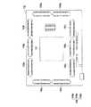
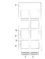
図1は本発明の一つの実施例のテストプラットフォームのブロック図である。図2は図1のテストプラットフォームの部分的な構造の側面図である。図3は図2のコントロールボードの平面図であり、わかりやすい表示と、説明のしやすさのために、図2はフィールドプログラマブル論理ゲートアレイボード130のうちの一つのソケットボード150に電気的に接続されていることを図示し、第二モニターポート141cによって見えない第二信号受信ポート141bを点線で表示している。図1から図3に示されるように、本実施例において、ユニバーサルテストプラットフォーム100は、ホスト110、コントロールボード120、フィールドプログラマブル論理ゲートアレイボード130、複数の第二ポート140と141、複数のソケットボード150、複数のNAND型フラッシュメモリ160を備え、ホスト110はデスクトップパソコン又はノートパソコンであっても良く、ケーブル10によりコントロールボード120の第一コネクタ124に接続され、それは例えばSATA(Serial Advanced Technology Attachment)やPCIe(Peripheral Component Interconnect Express)バスインターフェースである。 FIG. 1 is a block diagram of a test platform according to one embodiment of the present invention. FIG. 2 is a side view of a partial structure of the test platform of FIG. FIG. 3 is a plan view of the control board of FIG. 2, and FIG. 2 is electrically connected to one
詳細には、コントロールボード120はコントローラ121、2つのマルチデータレートSDRAM(DDRx
SDRAM)122、複数の第一ポート123を備え、コントローラ121は例えばSSD(solid state disk)コントローラであり、且つマルチデータレートSDRAM122、第一ポート123、第一コネクタ124とそれぞれ電気的に接続されている。従って、ホスト110は第一コネクタ124によりコントローラ121に電気的に接続され、コントローラ121とNAND型フラッシュメモリ160の制御とアクセスを行う。一方、マルチデータレートSDRAM122は例えば、ダブルデータレートSDRAM、トリプルデータレートSDRAM、クアドラプルデータレートSDRAM、又はさらにハイデータレートSDRAMであり、本発明はこれに対して制限をしない。Specifically, the
SDRAM) 122 and a plurality of first ports 123. The
図4は図2のフィールドプログラマブル論理ゲートアレイボードの平面図である。図2から図4に示されるように、フィールドプログラマブル論理ゲートアレイボード130はコントロールボード120と前記複数のソケットボード150の接続媒体となり、そのうちフィールドプログラマブル論理ゲートアレイボード130の向かい合う両側にペアで設置された前記複数の第二ポート140、141は主要な接続インターフェースとなる。詳細には、第一ポート123は複数の第一テストポート123aと第一信号受信ポート123bを備え、第二ポート140は複数の第二テストポート140aと第二信号受信ポート140bを備え、第一テストポート123aと第二テストポート140aは対応して設置され、且つ第一信号受信ポート123bと第二信号受信ポート140bは対応して設置される。 FIG. 4 is a plan view of the field programmable logic gate array board of FIG. As shown in FIGS. 2 to 4, the field programmable logic
同様に、第二ポート141も複数の第二テストポート141aと第二信号受信ポート141bを備え、第二テストポート140aと141aは、フィールドプログラマブル論理ゲートアレイボード130の向かい合う両側にペアで設置され、且つ第二信号受信ポート140bと141bは、フィールドプログラマブル論理ゲートアレイボード130の向かい合う両側にペアで設置される。ここで、フィールドプログラマブル論理ゲートアレイボード130のコントロールボード120側の各第二テストポート140aは対応する第一テストポート123aに接続され、各第二信号受信ポート140bは対応する第一信号受信ポート123bに接続され、フィールドプログラマブル論理ゲートアレイボード130とコントロールボード120を電気的に接続させる。図示していない実施例において、ケーブル又はそのほか適切な接続線で第二テストポート140aは対応する第一テストポート123aに接続され、第二信号受信ポート140bは対応する第一信号受信ポート123bに接続され、本発明はこれに対して制限をしない。 Similarly, the
図5は図2のソケットボードの平面図である。図1、図2、図5に示されるように、各ソケットボード150は、2つの第三ポート151と複数の接続域(又はコンセントと呼ぶ)152を備え、前記複数のNAND型フラッシュメモリ160は前記複数の接続域152にそれぞれ接続し、且つ各ソケットボード150上のNAND型フラッシュメモリ160はいずれも第三ポート151の同一側に位置する。NAND型フラッシュメモリ160は例えばソケットボード150上の接続域(コンセント)152に抜き差し可能に取り付けられるため、NAND型フラッシュメモリ160のテスト終了後、接続域(コンセント)152から容易に抜き去ることができ、はんだ除去の必要が無く、コロイド残留の問題も発生することなく、故にNAND型フラッシュメモリ160の構造の損傷を防ぐことができる。具体的には、各ソケットボード150は対応する2つの第三ポート151によりフィールドプログラマブル論理ゲートアレイボード130のコントロールボード120と反対側のいずれか2つの隣り合う第二テストポート141aに接続し、コントローラ121を第一テストポート123a、第二テストポート140aと141a、第三ポート151により各ソケットボード150上のNAND型フラッシュメモリ160に電気的に接続させる。且つ、コントローラ121が発信する制御信号は第一テストポート123aと第二テストポート140aを経てフィールドプログラマブル論理ゲートアレイボード130上の処理ユニット131に送られ、信号分析を行う。 FIG. 5 is a plan view of the socket board of FIG. 1, 2, and 5, each
一方、第一信号受信ポート123bは各マルチデータレートSDRAM122と電気的に接続し、各マルチデータレートSDRAM122のクロック信号を受信する。本実施例において、第一ポート123は第一モニターポート123cをさらに備え、第二ポート140は第一ポート123に対応して設置される第二モニターポート140cをさらに備え、同様に、第二ポート141は第二モニターポート140cに対応して設置される第二モニターポート141cをさらに備える。第一モニターポート123cとフィールドプログラマブル論理ゲートアレイボード130のコントロールボード120側の第二モニターポート140cは対応して設置されるため、第二モニターポート140cを第一モニターポート123cに接続された後、第一モニターポート123cは第二モニターポート140cにより第二モニターポート141cに電気的に接続され、第二モニターポート141cによりモニターモジュール170に電気的に接続される。ここで、第二モニターポート141cとモニターモジュール170との間の電気的な接続は例えばケーブル20により行われる。換言すると、コントローラ121がフィールドプログラマブル論理ゲートアレイボード130上の処理ユニット131に発信した制御信号が分析された後、その分析結果は第二モニターポート141cを経由してモニターモジュール170に送られ、表示される。さらに、コントローラ121が発信する制御信号も処理ユニット131に転送し、処理ユニット131を経て第二テストポート141aにより各ソケットボード150に迅速に送られ(図1及び図2に図示)、ソケットボード150上のNAND型フラッシュメモリ160をテストする。NAND型フラッシュメモリ160のテスト後のテスト結果はフィールドプログラマブル論理ゲートアレイボード130に返送され、それから第二モニターポート141cによりモニターモジュール170に送られ、表示される。従って、試験員はモニターモジュール170でコントローラ121が発信した制御信号の分析結果とNAND型フラッシュメモリ160のテスト結果を同時に観察でき、ファームウェア設計の正確性の比較と分析がしやくなる、又は必要な場合デバッグしやすくする。 On the other hand, the first
簡潔には、モジュール化されたユニバーサルテストプラットフォーム100の設計は、試験員に、供試のコントローラ121をコントロールボード120上に電気的に接続させ、供試のNAND型フラッシュメモリ160をソケットボード150上に電気的に接続させ、フィールドプログラマブル論理ゲートアレイボード130によりコントロールボード120とソケットボード150を電気的に接続させ、複数のソケットボード150上の複数の供試のNAND型フラッシュメモリ160をそれぞれテストする。従来のテスト装置は異なる型番のコントローラは逐一対応する回路の配置を設計する必要があることと比較し、且つコントローラとNAND型フラッシュメモリを同じ回路基板に設置する技術構成からすると、本実施例のモジュール化されたユニバーサルテストプラットフォーム100はコントローラ121のテスト効率を効果的に向上させ、テストコストを大幅に低下させる。 Briefly, the modular
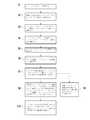
図6は図1のテストプラットフォームのフローチャート図である。図6及びそれに合う上述の図に示されるように、ユニバーサルテストプラットフォーム100のテスト方法は、ソケットボード150を提供するステップS1と、複数のNAND型フラッシュメモリ160をソケットボード150に電気的に接続されるステップS2を先行して行う。それから、ソケットボード150とフィールドプログラマブル論理ゲートアレイボード130を電気的に接続されるステップS3を行う。それから、フィールドプログラマブル論理ゲートアレイボード130とコントロールボード120を電気的に接続されるステップS4を行う。それから、コントロールボード120とホスト110を電気的に接続されるステップS5を行う。それから、モニターモジュール170とフィールドプログラマブル論理ゲートアレイボード130を電気的に接続されるステップS6を行う。それから、ホスト110により指示信号をコントロールボード120のコントローラ121に発信し、コントローラ121により指示信号を制御信号に変換するステップS7を行う。それから、制御信号をフィールドプログラマブル論理ゲートアレイボード130の処理ユニット131に書き込み、処理ユニット131により制御信号を各ソケットボード150に送り、各ソケットボード150上のNAND型フラッシュメモリ160をテストするステップS8を行う。ステップS8と同時に、処理ユニット131により制御信号を分析して、制御信号の分析結果をモニターモジュール170に表示するステップS9を行う。最後に、ソケットボード150上のNAND型フラッシュメモリ160のテスト結果をモニターモジュール170に表示し、モニターモジュール170に表示された制御信号の分析結果と比較するステップS10を行う。 FIG. 6 is a flowchart of the test platform of FIG. As shown in FIG. 6 and the above-mentioned figure corresponding thereto, the test method of the
以上のように、本発明のモジュール化されたユニバーサルテストプラットフォーム及びそのテスト方法は、試験員に供試のコントローラをコントロールボード上に電気的に接続させ、且つ供試のNAND型フラッシュメモリをソケットボード上に電気的に接続させ、フィールドプログラマブル論理ゲートアレイボードによりコントロールボードとソケットボードを電気的に接続させ、複数のソケットボード上の複数の供試のNAND型フラッシュメモリをそれぞれテストする。従来のテスト装置は異なる型番のコントローラは逐一対応する回路の配置の設計する必要があることと比較し、且つコントローラとNAND型フラッシュメモリを同じ回路基板に設置する技術構成からすると、本実施例のモジュール化されたユニバーサルテストプラットフォーム及びそのテスト方法はコントローラのテスト効率を効果的に向上させ、テストコストを大幅に低下させる。 As described above, the modular universal test platform and the test method thereof according to the present invention allow the tester to electrically connect the test controller to the control board and connect the test NAND flash memory to the socket board. The control board and the socket board are electrically connected to each other by a field programmable logic gate array board, and a plurality of test NAND flash memories on the plurality of socket boards are respectively tested. Compared with the need to design the circuit arrangement corresponding to the controller of the different model number for each of the conventional test devices, and from the technical configuration in which the controller and the NAND flash memory are installed on the same circuit board, The modularized universal test platform and its test method effectively improve the test efficiency of the controller and greatly reduce the test cost.
本発明は以上の実施例のように示したが、本発明は、これに限られるものではなく、当業者が本発明の精神の範囲から逸脱しない範囲において、変更又は修正することが可能であるが故に本発明の保護範囲は均等の範囲にまで及ぶものとする。 Although the present invention has been shown as in the above embodiments, the present invention is not limited to this and can be changed or modified by those skilled in the art without departing from the spirit of the present invention. Therefore, the protection scope of the present invention extends to an equivalent range.
本発明はテストプラットフォーム及びそのテスト方法に関するものであり、コントローラのテスト効率を効果的に向上させ、テストコストを大幅に低下させる。 The present invention relates to a test platform and a test method thereof, which effectively improves the test efficiency of a controller and greatly reduces the test cost.
10、20:ケーブル
100:ユニバーサルテストプラットフォーム
110:ホスト
120:コントロールボード
121:コントローラ
122:マルチデータレートSDRAM
123:第一ポート
123a:第一テストポート
123b:第一信号受信ポート
123c:第一モニターポート
124:第一コネクタ
130:フィールドプログラマブル論理ゲートアレイボード
131:処理ユニット
140、141:第二ポート
140a、141a:第二テストポート
140b、141b:第二信号受信ポート
140c、141c:第二モニターポート
150:ソケットボード
151:第三ポート
152:接続域
160:NAND型フラッシュメモリ
170:モニターモジュール
S1〜S10:ステップ10, 20: Cable 100: Universal test platform 110: Host 120: Control board 121: Controller 122: Multi data rate SDRAM
123:
本発明はユニバーサルテストプラットフォームを提供し、ホスト、コントロールボード、フィールドプログラマブル論理ゲートアレイ(field−programmable logic gate array)ボード、複数の第二ポート、複数のソケットボード、複数のNAND型フラッシュメモリを備える。コントロールボードはホストに電気的に接続され、且つコントローラと少なくとも一つのマルチデータレートSDRAM(Synchronous Dynamic Random Access Memory)と複数の第一ポートを備える。フィールドプログラマブル論理ゲートアレイボードは処理ユニットを備える。前記複数の第二ポートはフィールドプログラマブル論理ゲートアレイボードの向かい合う両側にペアで設置され、且つフィールドプログラマブル論理ゲートアレイボードの片側に位置する各第二ポートは対応する第一ポートに電気的に接続される。各ソケットボードは2つの第三ポートを備え、対応する前記2つの第三ポートにより、フィールドプログラマブル論理ゲートアレイボードのもう片側に位置するいずれか2つの隣り合う第二ポートに電気的に接続される。前記複数のNAND型フラッシュメモリはそれぞれ前記複数のソケットボードに接続される。The present invention provides a universal test platform, which includes a host, a control board, a field-programmable logic gate array board, a plurality of second ports, a plurality of socket boards, and a plurality of NAND flash memories. The control board is electrically connected to the host and includes a controller, at least one multi-data rate SDRAM (Synchronous Dynamic Random Access Memory), and a plurality of first ports. The field programmable logic gate array board includes a processing unit. The plurality of second ports are installed in pairs on opposite sides of the field programmable logic gate array board, and each second port locatedon one side of the field programmable logic gate array board is electrically connected to the corresponding first port. The Each socket board has two third ports and is electrically connected to any two adjacent second ports located on the other side of the field programmable logic gate array board by the corresponding two third ports. . The plurality of NAND flash memories are respectively connected to the plurality of socket boards.
本発明の一つの実施例において、前記第一ポートは複数の第一テストポートと第一信号受信ポートを備える。第二ポートは複数の第二テストポートと2つの第二信号受信ポートを備える。第一テストポートとフィールドプログラマブル論理ゲートアレイボードの片側に位置する第二テストポートは対応して設置され、且つ、第一信号受信ポートとフィールドプログラマブル論理ゲートアレイボードの片側に位置する第二信号受信ポートは対応して設置される。In one embodiment of the present invention, the first port includes a plurality of first test ports and a first signal receiving port. The second port includes a plurality of second test ports and two second signal reception ports. The first test port and the second test port locatedon one side of the field programmable logic gate array board are installed correspondingly, and the first signal reception port and the second signal reception located onone side of the field programmable logic gate array board Ports are installed correspondingly.
本発明の一つの実施例において、第一ポートは第一モニターポートをさらに備え、第二ポートは第二モニターポートをさらに備える。第一モニターポートとフィールドプログラマブル論理ゲートアレイボードの片側に位置する第二モニターポートは対応して設置される。In one embodiment of the invention, the first port further comprises a first monitor port and the second port further comprises a second monitor port. The first monitor port and the second monitor port locatedon one side of the field programmable logic gate array board are installed correspondingly.
本発明の一つの実施例において、前記ユニバーサルテストプラットフォームはモニターモジュールをさらに備え、フィールドプログラマブル論理ゲートアレイボードのもう片側に位置する第二モニターポートに電気的に接続され、且つフィールドプログラマブル論理ゲートアレイボードの片側に位置する第二モニターポートと第一モニターポートによりコントロールボードと電気的に接続される。In one embodiment of the present invention, the universal test platform further comprises a monitor module, electrically connected to a second monitor port located on the other side of the field programmable logic gate array board, and the field programmable logic gate array boardIs electrically connected to the control board by a second monitor port and a first monitor port locatedon one side .
Claims (9)
Translated fromJapanese前記ホストに電気的に接続され、コントローラと少なくとも一つのマルチデータレートSDRAMと複数の第一ポートを備えるコントロールボードと、
処理ユニットを備えるフィールドプログラマブル論理ゲートアレイボードと、
前記フィールドプログラマブル論理ゲートアレイボードの向かい合う両側にペアで設置され、それぞれ前記フィールドプログラマブル論理ゲートアレイボードのそのうち片側に位置し、対応する第一ポートに電気的に接続される複数の第二ポートと、
それぞれ2つの第三ポートを備え、対応する前記2つの第三ポートにより、前記フィールドプログラマブル論理ゲートアレイボードのもう片側に位置するいずれか2つの隣り合う前記第二ポートに電気的に接続される複数のソケットボードと、
それぞれ前記複数のソケットボードに接続される複数のNAND型フラッシュメモリと、
を備えることを特徴とするユニバーサルテストプラットフォーム。A host,
A control board electrically connected to the host, comprising a controller, at least one multi-data rate SDRAM, and a plurality of first ports;
A field programmable logic gate array board comprising a processing unit;
A plurality of second ports installed in pairs on opposite sides of the field programmable logic gate array board, each positioned on one side of the field programmable logic gate array board and electrically connected to a corresponding first port;
A plurality of two third ports each electrically connected to any two adjacent second ports located on the other side of the field programmable logic gate array board by the corresponding two third ports; Socket board,
A plurality of NAND flash memories respectively connected to the plurality of socket boards;
Universal test platform characterized by comprising:
複数のNAND型フラッシュメモリを前記複数のソケットボードにそれぞれ電気的に接続されるステップと、
前記ソケットボードとフィールドプログラマブル論理ゲートアレイボードを電気的に接続されるステップと、
前記フィールドプログラマブル論理ゲートアレイボードとコントロールボードを電気的に接続されるステップと、
前記コントロールボードと前記ホストを電気的に接続されるステップと、
前記ホストにより指示信号を前記コントロールボードに発信するステップと、
前記コントロールボード上のコントローラにより前記指示信号を制御信号に変換するステップと、
前記制御信号を前記フィールドプログラマブル論理ゲートアレイボードの処理ユニットに書き込み、且つ前記処理ユニットにより前記制御信号を前記各ソケットボードに送り、前記各ソケットボード上の前記複数のNAND型フラッシュメモリをテストするステップと、
を含むことを特徴とするユニバーサルテストプラットフォームのテスト方法。Providing a plurality of socket boards;
Electrically connecting a plurality of NAND flash memories to each of the plurality of socket boards;
Electrically connecting the socket board and the field programmable logic gate array board;
Electrically connecting the field programmable logic gate array board and the control board;
Electrically connecting the control board and the host;
Sending an instruction signal to the control board by the host;
Converting the instruction signal into a control signal by a controller on the control board;
Writing the control signal to a processing unit of the field programmable logic gate array board and sending the control signal to the socket boards by the processing unit to test the plurality of NAND flash memories on the socket boards; When,
A test method for a universal test platform characterized by comprising:
Applications Claiming Priority (2)
| Application Number | Priority Date | Filing Date | Title |
|---|---|---|---|
| TW104105859 | 2015-02-24 | ||
| TW104105859ATWI510798B (en) | 2015-02-24 | 2015-02-24 | Universal test platform and test method thereof |
Publications (2)
| Publication Number | Publication Date |
|---|---|
| JP2016156798Atrue JP2016156798A (en) | 2016-09-01 |
| JP6033913B2 JP6033913B2 (en) | 2016-11-30 |
Family
ID=55407752
Family Applications (1)
| Application Number | Title | Priority Date | Filing Date |
|---|---|---|---|
| JP2015088847AExpired - Fee RelatedJP6033913B2 (en) | 2015-02-24 | 2015-04-24 | Universal test platform and test method thereof |
Country Status (3)
| Country | Link |
|---|---|
| JP (1) | JP6033913B2 (en) |
| CN (1) | CN106199374A (en) |
| TW (1) | TWI510798B (en) |
Cited By (6)
| Publication number | Priority date | Publication date | Assignee | Title |
|---|---|---|---|---|
| CN106199374A (en)* | 2015-02-24 | 2016-12-07 | 力成科技股份有限公司 | Universal test platform and test method thereof |
| CN109323716A (en)* | 2018-11-01 | 2019-02-12 | 上海开通数控有限公司 | The serial absolute type encoder of servo drive system detects debugging apparatus |
| CN112509631A (en)* | 2020-12-25 | 2021-03-16 | 东莞记忆存储科技有限公司 | Batch testing system and method for quality of storage particles, computer equipment and storage medium |
| CN115080282A (en)* | 2022-06-17 | 2022-09-20 | 安徽帝晶光电科技有限公司 | Integrated modular multi-model test platform system |
| US20230060664A1 (en) | 2021-08-26 | 2023-03-02 | Western Digital Technologies, Inc. | Testing apparatus for temperature testing of electronic devices |
| US11698408B2 (en) | 2021-08-26 | 2023-07-11 | Western Digital Technologies, Inc. | Testing apparatus for data storage devices |
Families Citing this family (1)
| Publication number | Priority date | Publication date | Assignee | Title |
|---|---|---|---|---|
| CN114721597A (en)* | 2022-04-07 | 2022-07-08 | 深圳宏芯宇电子股份有限公司 | Modular flash memory device |
Citations (2)
| Publication number | Priority date | Publication date | Assignee | Title |
|---|---|---|---|---|
| JPH08146080A (en)* | 1994-11-28 | 1996-06-07 | Sumitomo Electric Ind Ltd | Burn-in board |
| JP2007201471A (en)* | 1998-12-31 | 2007-08-09 | Formfactor Inc | Method of testing semiconductor product die, and assembly including test die for its test |
Family Cites Families (9)
| Publication number | Priority date | Publication date | Assignee | Title |
|---|---|---|---|---|
| CN1609862A (en)* | 2004-11-19 | 2005-04-27 | 华南理工大学 | PCI bus-based IP core simulation verification platform and its verification method |
| TW200828325A (en)* | 2006-12-18 | 2008-07-01 | Golden Emperor Internat Ltd | System and method for testing memories |
| CN101334448B (en)* | 2008-05-23 | 2012-07-04 | 深圳市同洲电子股份有限公司 | Test platform and method for testing PC board |
| TWI440036B (en)* | 2010-01-20 | 2014-06-01 | King Yuan Electronics Co Ltd | Memory test equipment with extensible sample memory |
| CN102201267A (en)* | 2010-03-26 | 2011-09-28 | 上海摩波彼克半导体有限公司 | Platform system for realizing circuit verification of Nandflash flash memory controller based on FPGA (Field Programmable Gate Array) and method thereof |
| TWI469151B (en)* | 2011-08-26 | 2015-01-11 | Powertech Technology Inc | Testing interface board specially for dram memory packages |
| CN102332311B (en)* | 2011-10-18 | 2013-10-02 | 中国航天科技集团公司第五研究院第五一〇研究所 | FPGA (Field Programmable Gate Array)-based single event effect test method for NAND FLASH device |
| CN103809106A (en)* | 2012-11-15 | 2014-05-21 | 佛山市顺德区顺达电脑厂有限公司 | Automatic test device and method |
| TWI510798B (en)* | 2015-02-24 | 2015-12-01 | Powertech Technology Inc | Universal test platform and test method thereof |
- 2015
- 2015-02-24TWTW104105859Apatent/TWI510798B/ennot_activeIP Right Cessation
- 2015-04-24JPJP2015088847Apatent/JP6033913B2/ennot_activeExpired - Fee Related
- 2015-05-08CNCN201510230525.9Apatent/CN106199374A/enactivePending
Patent Citations (2)
| Publication number | Priority date | Publication date | Assignee | Title |
|---|---|---|---|---|
| JPH08146080A (en)* | 1994-11-28 | 1996-06-07 | Sumitomo Electric Ind Ltd | Burn-in board |
| JP2007201471A (en)* | 1998-12-31 | 2007-08-09 | Formfactor Inc | Method of testing semiconductor product die, and assembly including test die for its test |
Cited By (8)
| Publication number | Priority date | Publication date | Assignee | Title |
|---|---|---|---|---|
| CN106199374A (en)* | 2015-02-24 | 2016-12-07 | 力成科技股份有限公司 | Universal test platform and test method thereof |
| CN109323716A (en)* | 2018-11-01 | 2019-02-12 | 上海开通数控有限公司 | The serial absolute type encoder of servo drive system detects debugging apparatus |
| CN109323716B (en)* | 2018-11-01 | 2023-12-29 | 上海电气集团自动化工程有限公司 | Detection and debugging device for serial absolute encoder of servo driving system |
| CN112509631A (en)* | 2020-12-25 | 2021-03-16 | 东莞记忆存储科技有限公司 | Batch testing system and method for quality of storage particles, computer equipment and storage medium |
| US20230060664A1 (en) | 2021-08-26 | 2023-03-02 | Western Digital Technologies, Inc. | Testing apparatus for temperature testing of electronic devices |
| US11698408B2 (en) | 2021-08-26 | 2023-07-11 | Western Digital Technologies, Inc. | Testing apparatus for data storage devices |
| US11828793B2 (en) | 2021-08-26 | 2023-11-28 | Western Digital Technologies, Inc. | Testing apparatus for temperature testing of electronic devices |
| CN115080282A (en)* | 2022-06-17 | 2022-09-20 | 安徽帝晶光电科技有限公司 | Integrated modular multi-model test platform system |
Also Published As
| Publication number | Publication date |
|---|---|
| TWI510798B (en) | 2015-12-01 |
| CN106199374A (en) | 2016-12-07 |
| JP6033913B2 (en) | 2016-11-30 |
| TW201631325A (en) | 2016-09-01 |
Similar Documents
| Publication | Publication Date | Title |
|---|---|---|
| JP6033913B2 (en) | Universal test platform and test method thereof | |
| US9535117B2 (en) | System debug using an all-in-one connector | |
| US9285427B2 (en) | Testing apparatus and testing method of electronic device | |
| US11828787B2 (en) | Eye diagram capture test during production | |
| JP2015025805A (en) | High speed tester communication interface between test slice and tray | |
| TW201621657A (en) | Electronic device | |
| CN103365751A (en) | Main board testing device and changeover module thereof | |
| CN102929755B (en) | Fault detection method of CPU (Central Processing Unit) module address and data bus | |
| CN111124768B (en) | Method and apparatus for accessing high-capacity test data via a high-speed interface | |
| TWI772643B (en) | Device and method for testing a computer system | |
| CN108153624B (en) | Test circuit board suitable for NGFF slot | |
| CN107943734A (en) | A kind of more FPGA isomeries accelerator card debugging systems and its interface connecting method, system | |
| US11953550B2 (en) | Server JTAG component adaptive interconnection system and method | |
| US10379139B2 (en) | Methods, systems and devices for testing circuit modules using a microbackplane interface | |
| US9158609B2 (en) | Universal serial bus testing device | |
| TW201502767A (en) | Detecting system and method for server motherboard | |
| CN115906733A (en) | Universal bottom plate design based on standard COMe | |
| CN107886996A (en) | A kind of method of batch testing NVME hard disks | |
| TWM556332U (en) | Chip test board and chip test system | |
| TWI459012B (en) | Testing device having plurality of connecting ports | |
| TWI881599B (en) | Universal detection system providing different types of connection interface and method thereof | |
| CN201096807Y (en) | Adapter | |
| TW201624282A (en) | Electronic device | |
| CN102567150A (en) | Main board interface testing device | |
| TW201624283A (en) | Electronic device |
Legal Events
| Date | Code | Title | Description |
|---|---|---|---|
| TRDD | Decision of grant or rejection written | ||
| A01 | Written decision to grant a patent or to grant a registration (utility model) | Free format text:JAPANESE INTERMEDIATE CODE: A01 Effective date:20161004 | |
| A61 | First payment of annual fees (during grant procedure) | Free format text:JAPANESE INTERMEDIATE CODE: A61 Effective date:20161026 | |
| R150 | Certificate of patent or registration of utility model | Ref document number:6033913 Country of ref document:JP Free format text:JAPANESE INTERMEDIATE CODE: R150 | |
| LAPS | Cancellation because of no payment of annual fees |