JP2016143853A - Multilayer semiconductor device - Google Patents
Multilayer semiconductor deviceDownload PDFInfo
- Publication number
- JP2016143853A JP2016143853AJP2015021119AJP2015021119AJP2016143853AJP 2016143853 AJP2016143853 AJP 2016143853AJP 2015021119 AJP2015021119 AJP 2015021119AJP 2015021119 AJP2015021119 AJP 2015021119AJP 2016143853 AJP2016143853 AJP 2016143853A
- Authority
- JP
- Japan
- Prior art keywords
- decoupling
- electrode
- power supply
- integrated circuit
- transmission line
- Prior art date
- Legal status (The legal status is an assumption and is not a legal conclusion. Google has not performed a legal analysis and makes no representation as to the accuracy of the status listed.)
- Pending
Links
Images


Classifications
- H—ELECTRICITY
- H01—ELECTRIC ELEMENTS
- H01L—SEMICONDUCTOR DEVICES NOT COVERED BY CLASS H10
- H01L25/00—Assemblies consisting of a plurality of semiconductor or other solid state devices
- H01L25/03—Assemblies consisting of a plurality of semiconductor or other solid state devices all the devices being of a type provided for in a single subclass of subclasses H10B, H10D, H10F, H10H, H10K or H10N, e.g. assemblies of rectifier diodes
- H01L25/04—Assemblies consisting of a plurality of semiconductor or other solid state devices all the devices being of a type provided for in a single subclass of subclasses H10B, H10D, H10F, H10H, H10K or H10N, e.g. assemblies of rectifier diodes the devices not having separate containers
- H01L25/065—Assemblies consisting of a plurality of semiconductor or other solid state devices all the devices being of a type provided for in a single subclass of subclasses H10B, H10D, H10F, H10H, H10K or H10N, e.g. assemblies of rectifier diodes the devices not having separate containers the devices being of a type provided for in group H10D89/00
- H01L25/0657—Stacked arrangements of devices
- H—ELECTRICITY
- H01—ELECTRIC ELEMENTS
- H01L—SEMICONDUCTOR DEVICES NOT COVERED BY CLASS H10
- H01L23/00—Details of semiconductor or other solid state devices
- H01L23/52—Arrangements for conducting electric current within the device in operation from one component to another, i.e. interconnections, e.g. wires, lead frames
- H01L23/522—Arrangements for conducting electric current within the device in operation from one component to another, i.e. interconnections, e.g. wires, lead frames including external interconnections consisting of a multilayer structure of conductive and insulating layers inseparably formed on the semiconductor body
- H01L23/5222—Capacitive arrangements or effects of, or between wiring layers
- H01L23/5223—Capacitor integral with wiring layers
- H—ELECTRICITY
- H01—ELECTRIC ELEMENTS
- H01L—SEMICONDUCTOR DEVICES NOT COVERED BY CLASS H10
- H01L23/00—Details of semiconductor or other solid state devices
- H01L23/52—Arrangements for conducting electric current within the device in operation from one component to another, i.e. interconnections, e.g. wires, lead frames
- H01L23/522—Arrangements for conducting electric current within the device in operation from one component to another, i.e. interconnections, e.g. wires, lead frames including external interconnections consisting of a multilayer structure of conductive and insulating layers inseparably formed on the semiconductor body
- H01L23/5228—Resistive arrangements or effects of, or between, wiring layers
- H—ELECTRICITY
- H01—ELECTRIC ELEMENTS
- H01L—SEMICONDUCTOR DEVICES NOT COVERED BY CLASS H10
- H01L23/00—Details of semiconductor or other solid state devices
- H01L23/58—Structural electrical arrangements for semiconductor devices not otherwise provided for, e.g. in combination with batteries
- H01L23/64—Impedance arrangements
- H01L23/642—Capacitive arrangements
- H—ELECTRICITY
- H01—ELECTRIC ELEMENTS
- H01L—SEMICONDUCTOR DEVICES NOT COVERED BY CLASS H10
- H01L23/00—Details of semiconductor or other solid state devices
- H01L23/58—Structural electrical arrangements for semiconductor devices not otherwise provided for, e.g. in combination with batteries
- H01L23/64—Impedance arrangements
- H01L23/647—Resistive arrangements
- H—ELECTRICITY
- H01—ELECTRIC ELEMENTS
- H01L—SEMICONDUCTOR DEVICES NOT COVERED BY CLASS H10
- H01L2224/00—Indexing scheme for arrangements for connecting or disconnecting semiconductor or solid-state bodies and methods related thereto as covered by H01L24/00
- H01L2224/01—Means for bonding being attached to, or being formed on, the surface to be connected, e.g. chip-to-package, die-attach, "first-level" interconnects; Manufacturing methods related thereto
- H01L2224/10—Bump connectors; Manufacturing methods related thereto
- H01L2224/15—Structure, shape, material or disposition of the bump connectors after the connecting process
- H01L2224/16—Structure, shape, material or disposition of the bump connectors after the connecting process of an individual bump connector
- H01L2224/161—Disposition
- H01L2224/16135—Disposition the bump connector connecting between different semiconductor or solid-state bodies, i.e. chip-to-chip
- H01L2224/16145—Disposition the bump connector connecting between different semiconductor or solid-state bodies, i.e. chip-to-chip the bodies being stacked
- H—ELECTRICITY
- H01—ELECTRIC ELEMENTS
- H01L—SEMICONDUCTOR DEVICES NOT COVERED BY CLASS H10
- H01L2224/00—Indexing scheme for arrangements for connecting or disconnecting semiconductor or solid-state bodies and methods related thereto as covered by H01L24/00
- H01L2224/01—Means for bonding being attached to, or being formed on, the surface to be connected, e.g. chip-to-package, die-attach, "first-level" interconnects; Manufacturing methods related thereto
- H01L2224/10—Bump connectors; Manufacturing methods related thereto
- H01L2224/15—Structure, shape, material or disposition of the bump connectors after the connecting process
- H01L2224/16—Structure, shape, material or disposition of the bump connectors after the connecting process of an individual bump connector
- H01L2224/161—Disposition
- H01L2224/16151—Disposition the bump connector connecting between a semiconductor or solid-state body and an item not being a semiconductor or solid-state body, e.g. chip-to-substrate, chip-to-passive
- H01L2224/16221—Disposition the bump connector connecting between a semiconductor or solid-state body and an item not being a semiconductor or solid-state body, e.g. chip-to-substrate, chip-to-passive the body and the item being stacked
- H01L2224/16225—Disposition the bump connector connecting between a semiconductor or solid-state body and an item not being a semiconductor or solid-state body, e.g. chip-to-substrate, chip-to-passive the body and the item being stacked the item being non-metallic, e.g. insulating substrate with or without metallisation
- H01L2224/16227—Disposition the bump connector connecting between a semiconductor or solid-state body and an item not being a semiconductor or solid-state body, e.g. chip-to-substrate, chip-to-passive the body and the item being stacked the item being non-metallic, e.g. insulating substrate with or without metallisation the bump connector connecting to a bond pad of the item
- H—ELECTRICITY
- H01—ELECTRIC ELEMENTS
- H01L—SEMICONDUCTOR DEVICES NOT COVERED BY CLASS H10
- H01L2225/00—Details relating to assemblies covered by the group H01L25/00 but not provided for in its subgroups
- H01L2225/03—All the devices being of a type provided for in the same main group of the same subclass of class H10, e.g. assemblies of rectifier diodes
- H01L2225/04—All the devices being of a type provided for in the same main group of the same subclass of class H10, e.g. assemblies of rectifier diodes the devices not having separate containers
- H01L2225/065—All the devices being of a type provided for in the same main group of the same subclass of class H10
- H01L2225/06503—Stacked arrangements of devices
- H01L2225/06527—Special adaptation of electrical connections, e.g. rewiring, engineering changes, pressure contacts, layout
- H—ELECTRICITY
- H01—ELECTRIC ELEMENTS
- H01L—SEMICONDUCTOR DEVICES NOT COVERED BY CLASS H10
- H01L2225/00—Details relating to assemblies covered by the group H01L25/00 but not provided for in its subgroups
- H01L2225/03—All the devices being of a type provided for in the same main group of the same subclass of class H10, e.g. assemblies of rectifier diodes
- H01L2225/04—All the devices being of a type provided for in the same main group of the same subclass of class H10, e.g. assemblies of rectifier diodes the devices not having separate containers
- H01L2225/065—All the devices being of a type provided for in the same main group of the same subclass of class H10
- H01L2225/06503—Stacked arrangements of devices
- H01L2225/06541—Conductive via connections through the device, e.g. vertical interconnects, through silicon via [TSV]
Landscapes
- Engineering & Computer Science (AREA)
- Power Engineering (AREA)
- Microelectronics & Electronic Packaging (AREA)
- Physics & Mathematics (AREA)
- Condensed Matter Physics & Semiconductors (AREA)
- General Physics & Mathematics (AREA)
- Computer Hardware Design (AREA)
- Semiconductor Integrated Circuits (AREA)
Abstract
Description
Translated fromJapanese本発明は、積層型半導体装置に関する。 The present invention relates to a stacked semiconductor device.
従来、基板上に搭載するべく複数のLSIチップ等の集積回路チップを積層した半導体装置がある。
また、集積回路の電源ノイズやグラウンドノイズを除去するために電源とグラウンドの間に接続されたデカップリングコンデンサを設けることがある。
また、基板上に搭載するべく複数の集積回路チップを積層した半導体装置において、各集積回路チップに設けられ、互いに接続されたビアホールに、最上層の集積回路チップ上に搭載されたデカップリングコンデンサを接続することも提案されている。Conventionally, there is a semiconductor device in which a plurality of integrated circuit chips such as LSI chips are stacked for mounting on a substrate.
Further, a decoupling capacitor connected between the power source and the ground may be provided in order to remove power source noise and ground noise of the integrated circuit.
Further, in a semiconductor device in which a plurality of integrated circuit chips are stacked for mounting on a substrate, a decoupling capacitor mounted on the uppermost integrated circuit chip is provided in a via hole provided in each integrated circuit chip and connected to each other. It has also been proposed to connect.
しかしながら、基板上に搭載するべく複数の集積回路チップを積層した半導体装置において、各集積回路チップに設けられ、互いに接続された貫通電極配線を通してデカップリングコンデンサを接続しても、貫通電極配線のインダクタンス成分に起因して、良好な高周波電源ノイズや高周波グラウンドノイズの低減効果が得られない。以下、電源ノイズという用語には通常グラウンドノイズの意味も含まれていることとする。 However, in a semiconductor device in which a plurality of integrated circuit chips are stacked for mounting on a substrate, even if a decoupling capacitor is connected to each other through the through-electrode wirings connected to each other, the inductance of the through-electrode wiring Due to the components, good high frequency power supply noise and high frequency ground noise reduction effects cannot be obtained. Hereinafter, the term power supply noise usually includes the meaning of ground noise.
そこで、良好な高周波電源ノイズの低減効果が得られるようにしたい。 Therefore, it is desirable to obtain a good effect of reducing high frequency power supply noise.
本積層型半導体装置は、基板上に積層された複数の集積回路チップを備え、複数の集積回路チップの中の電源供給対象チップの電源端子及びグランド端子は、それぞれ、デカップリング用電源側貫通電極配線及びデカップリング用グランド側貫通電極配線に接続され、デカップリング用電源側貫通電極配線とデカップリング用グランド側貫通電極配線とによってデカップリング用貫通電極伝送線路が構成され、デカップリング用貫通電極伝送線路の終端に位置する集積回路チップ上で、デカップリング用貫通電極伝送線路の特性インピーダンスと等しい抵抗及び容量が直列で接続されている。 The stacked semiconductor device includes a plurality of integrated circuit chips stacked on a substrate, and a power supply terminal and a ground terminal of a power supply target chip among the plurality of integrated circuit chips are each a decoupling power supply side through electrode The decoupling through electrode transmission line is configured by the power supply side through electrode wiring for decoupling and the ground side through electrode wiring for decoupling, and connected to the ground side through electrode wiring for decoupling. On the integrated circuit chip located at the end of the line, resistors and capacitors equal to the characteristic impedance of the decoupling through-electrode transmission line are connected in series.
したがって、本積層型半導体装置によれば、良好な高周波電源ノイズの低減効果が得られるという利点がある。 Therefore, according to the present stacked semiconductor device, there is an advantage that a good effect of reducing high frequency power supply noise can be obtained.
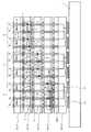
以下、図面により、本発明の実施の形態にかかる積層型半導体装置について、図1を参照しながら説明する。
本実施形態の積層型半導体装置は、図1に示すように、基板1上に搭載するべく積層された複数の集積回路チップ2を備える。これらの複数の集積回路チップ2の中の電源供給対象チップ2B〜2Dの電源端子3及びグランド端子4は、それぞれ、デカップリング用電源側貫通電極配線5及びデカップリング用グランド側貫通電極配線6に接続されている。また、デカップリング用電源側貫通電極配線5とデカップリング用グランド側貫通電極配線6とによってデカップリング用貫通電極伝送線路7が構成される。そして、デカップリング用貫通電極伝送線路7の終端に位置する集積回路チップ上で、デカップリング用貫通電極伝送線路7の特性インピーダンスと等しい抵抗8及び容量9が直列で接続されている。なお、積層型半導体装置を、3次元積層構造の半導体装置、積層型半導体集積回路、積層LSI、3D−LSIともいう。A stacked semiconductor device according to an embodiment of the present invention will be described below with reference to FIG.
As shown in FIG. 1, the stacked semiconductor device of this embodiment includes a plurality of
ここで、集積回路チップ2は、例えばLSIチップなどの半導体集積回路チップ、例えばSiやガラスなどの基板に微細な配線や受動素子が形成されたインタポーザや集積回路チップなどである。なお、LSIチップとは、LSIのパッケージを含まないLSIのダイを意味することとする。
本実施形態では、基板1上に搭載するべく、5つの集積回路チップ2A〜2Eが積層され、互いに接続されており、最も上側の集積回路チップ2Eと最も下側(基板側)の集積回路チップ2Aとの間の3つの集積回路チップ2B〜2Dを電源供給対象チップとする場合を例に挙げて説明する。Here, the
In the present embodiment, five
なお、ここでは、最も下側の集積回路チップ(最下層の集積回路チップ)2Aはインタポーザであり、下から2番目から4番目の集積回路チップ(第2層から第4層の集積回路チップ)2B〜2DはLSIチップである。また、最も上側の集積回路チップ(最上層の集積回路チップ)2EはLSIチップであっても良いし、Siやガラス等の基板に受動素子が形成された集積回路チップであっても良い。なお、最も下側の集積回路チップ2Aには、集積回路チップ2B〜2Eが積層された場所とは異なる場所に、他の電子部品や集積回路が積層され、これらの間を接続する配線が形成されていても良い。また、最も下側の集積回路チップ2Aは、LSIチップであっても良い。 Here, the lowermost integrated circuit chip (lowermost integrated circuit chip) 2A is an interposer, and the second to fourth integrated circuit chips from the bottom (integrated circuit chips from the second layer to the fourth layer). 2B to 2D are LSI chips. The uppermost integrated circuit chip (uppermost integrated circuit chip) 2E may be an LSI chip or an integrated circuit chip in which passive elements are formed on a substrate such as Si or glass. In the lowermost
また、ここでは、符号Xで示す領域が、下から2番目の集積回路チップ2Bに対する電源供給及びデカップリングのための電源構造である。また、符号Yで示す領域が、下から3番目の集積回路チップ2Cに対する電源供給及びデカップリングのための電源構造である。また、符号Zで示す領域が、下から4番目の集積回路チップ2Dに対する電源供給及びデカップリングのための電源構造である。 Further, here, the region indicated by the symbol X is a power supply structure for power supply and decoupling to the second integrated
ここでは、下から2番目の集積回路チップ2Bに対する電源供給及びデカップリングのための電源構造(図1中、符号Xで示す領域)は、以下のようになっている。
つまり、最も下側の集積回路チップ2Aは、電源側下面電極2Aaと、電源側上面電極2Abと、これらを接続する電源側配線2Acとを備える。
また、電源供給対象チップである下から2番目の集積回路チップ2Bは、電源側下面電極2Baと、電源側上面電極2Bbと、これらを接続する電源側貫通電極2Bcとを備え、電源側貫通電極2Bcにチップ内電源配線2BX(図1中、点線で囲まれた領域参照)が接続されている。Here, the power supply structure for power supply and decoupling to the second integrated
That is, the lowermost
The second integrated
そして、基板1上に設けられ、電源に接続された電源電極1Xに、最も下側の集積回路チップ2Aの電源側下面電極2Aaが接続されており、さらに、最も下側の集積回路チップ2Aの電源側上面電極2Abに、下から2番目の集積回路チップ2Bの電源側下面電極2Baが接続されている。
これにより、基板1上の電源電極1Xに、最も下側の集積回路チップ2Aの電源側下面電極2Aa、電源側配線2Ac及び電源側上面電極2Ab、並びに、下から2番目の集積回路チップ2Bの電源側下面電極2Ba及び電源側貫通電極2Bcを介して、下から2番目の集積回路チップ2Bのチップ内電源配線2BXが接続され、下から2番目の集積回路チップ2B内に電源供給が行なわれるようになっている。Then, the power supply side lower surface electrode 2Aa of the lowermost
As a result, the
このため、下から2番目の集積回路チップ2Bの電源側貫通電極2Bcのチップ内電源配線2BXが接続されている部分を、電極端子3という。また、最も下側の集積回路チップ2Aの電源側下面電極2Aa、電源側配線2Ac及び電源側上面電極2Ab、並びに、下から2番目の集積回路チップ2Bの電源側下面電極2Ba、電源側貫通電極2Bcのチップ内電源配線2BXが接続されている部分までが、電源配線となる。 Therefore, the portion of the power supply side through electrode 2Bc of the second integrated
また、最も下側の集積回路チップ2Aは、グランド側下面電極2Adと、グランド側上面電極2Aeと、これらを接続するグランド側配線2Afとを備える。
また、電源供給対象チップである下から2番目の集積回路チップ2Bは、グランド側下面電極2Bdと、グランド側上面電極2Beと、これらを接続するグランド側貫通電極2Bfとを備え、グランド側貫通電極2Bfにチップ内グランド配線2BY(図1中、点線で囲まれた領域参照)が接続されている。The lowermost
The second integrated
そして、基板1上に設けられ、グランドに接続されたグランド電極1Yに、最も下側の集積回路チップ2Aのグランド側下面電極2Adが接続されており、さらに、最も下側の集積回路チップ2Aのグランド側上面電極2Aeに、下から2番目の集積回路チップ2Bのグランド側下面電極2Bdが接続されている。
これにより、基板1上のグランド電極1Yに、最も下側の集積回路チップ2Aのグランド側下面電極2Ad、グランド側配線2Af及びグランド側上面電極2Ae、並びに、下から2番目の集積回路チップ2Bのグランド側下面電極2Bd及びグランド側貫通電極2Bfを介して、下から2番目の集積回路チップ2Bのチップ内グランド配線2BYが接続されている。The ground-side lower surface electrode 2Ad of the lowermost
Accordingly, the ground-side lower surface electrode 2Ad, the ground-side wiring 2Af, the ground-side upper surface electrode 2Ae of the lowermost
このため、下から2番目の集積回路チップ2Bのグランド側貫通電極2Bfのチップ内グランド配線2BYが接続されている部分を、グランド端子4という。また、最も下側の集積回路チップ2Aのグランド側下面電極2Ad、グランド側配線2Af及びグランド側上面電極2Ae、並びに、下から2番目の集積回路チップ2Bのグランド側下面電極2Bd、グランド側貫通電極2Bfのチップ内グランド配線2BYが接続されている部分までが、グランド配線となる。 For this reason, the part to which the in-chip ground wiring 2BY of the ground side through electrode 2Bf of the second integrated
また、下から3番目、4番目の集積回路チップ2C、2D、最も上側の集積回路チップ2Eは、それぞれ、電源側下面電極2Ca、2Da、2Eaと、電源側上面電極2Cb、2Db、2Ebと、これらを接続する電源側貫通電極2Cc、2Dc、2Ecとを備える。
そして、下から2番目の集積回路チップ2Bの電源側上面電極2Bbに、下から3番目の集積回路チップ2Cの電源側下面電極2Caが接続されており、下から3番目の集積回路チップ2Cの電源側上面電極2Cbに、下から4番目の集積回路チップ2Dの電源側下面電極2Daが接続されており、下から4番目の集積回路チップ2Dの電源側上面電極2Dbに、最も上側の集積回路チップ2Eの電源側下面電極2Eaが接続されている。Further, the third to fourth
Then, the power supply side lower surface electrode 2Ca of the third
これにより、下から2番目の集積回路チップ2Bの電源側貫通電極2Bcのチップ内電源配線2BXが接続されている部分よりも上方の部分及び電源側上面電極2Bb、下から3番目の集積回路チップ2Cの電源側下面電極2Ca、電源側貫通電極2Cc及び電源側上面電極2Cb、下から4番目の集積回路チップ2Dの電源側下面電極2Da、電源側貫通電極2Dc及び電源側上面電極2Db、最も上側の集積回路チップ2Eの電源側下面電極2Ea、電源側貫通電極2Ecが、下から2番目の集積回路チップ2Bの電源端子3に接続されている。 As a result, the upper part of the power supply side through electrode 2Bc of the second
つまり、下から2番目の集積回路チップ2Bの電源側貫通電極2Bcのチップ内電源配線2BXが接続されている部分よりも上方の部分及び電源側上面電極2Bb、下から3番目の集積回路チップ2Cの電源側下面電極2Ca、電源側貫通電極2Cc及び電源側上面電極2Cb、下から4番目の集積回路チップ2Dの電源側下面電極2Da、電源側貫通電極2Dc及び電源側上面電極2Db、最も上側の集積回路チップ2Eの電源側下面電極2Ea、電源側貫通電極2Ecによって、即ち、複数の電源側貫通電極2Bc、2Cc、2Dc、2Ecを接続したものによってデカップリング用電源側貫通電極配線5が構成され、このデカップリング用電源側貫通電極配線5が、電源供給対象チップである下から2番目の集積回路チップ2Bの電源端子3に接続されている。 That is, the power supply side upper electrode 2Bb of the power supply side through electrode 2Bc of the second
この場合、デカップリング用電源側貫通電極配線5は、電源供給対象チップである下から2番目の集積回路チップ2Bの上側へ延びており、電源供給対象チップである下から2番目の集積回路チップ2Bから最も上側の集積回路チップ2Eまで各集積回路チップを貫通して延びていることになる。
また、下から3番目、4番目の集積回路チップ2C、2D、最も上側の集積回路チップ2Eは、グランド側下面電極2Cd、2Dd、2Edと、グランド側上面電極2Ce、2De、2Eeと、これらを接続するグランド側貫通電極2Cf、2Df、2Efとを備える。In this case, the decoupling power supply side through
The third to fourth
そして、下から2番目の集積回路チップ2Bのグランド側上面電極2Beに、下から3番目の集積回路チップ2Cのグランド側下面電極2Cdが接続されており、下から3番目の集積回路チップ2Cのグランド側上面電極2Ceに、下から4番目の集積回路チップ2Dのグランド側下面電極2Ddが接続されており、下から4番目の集積回路チップ2Dのグランド側上面電極2Deに、最も上側の集積回路チップ2Eのグランド側下面電極2Edが接続されている。 Then, the ground side lower surface electrode 2Cd of the third
これにより、下から2番目の集積回路チップ2Bのグランド側貫通電極2Bfのチップ内グランド配線2BYが接続されている部分よりも上方の部分及びグランド側上面電極2Be、下から3番目の集積回路チップ2Cのグランド側下面電極2Cd、グランド側貫通電極2Cf及びグランド側上面電極2Ce、下から4番目の集積回路チップ2Dのグランド側下面電極2Dd、グランド側貫通電極2Df及びグランド側上面電極2De、最も上側の集積回路チップ2Eのグランド側下面電極2Ed、グランド側貫通電極2Efが、下から2番目の集積回路チップ2Bのグランド端子4に接続されている。 As a result, the upper part of the ground-side through electrode 2Bf of the second
つまり、下から2番目の集積回路チップ2Bのグランド側貫通電極2Bfのチップ内グランド配線2BYが接続されている部分よりも上方の部分及びグランド側上面電極2Be、下から3番目の集積回路チップ2Cのグランド側下面電極2Cd、グランド側貫通電極2Cf及びグランド側上面電極2Ce、下から4番目の集積回路チップ2Dのグランド側下面電極2Dd、グランド側貫通電極2Df及びグランド側上面電極2De、最も上側の集積回路チップ2Eのグランド側下面電極2Ed、グランド側貫通電極2Efによって、即ち、複数のグランド側貫通電極2Bf、2Cf、2Df、2Efを接続したものによってデカップリング用グランド側貫通電極配線6が構成され、このデカップリング用グランド側貫通電極配線6が、電源供給対象チップである下から2番目の集積回路チップ2Bのグランド端子4に接続されている。 That is, the upper part of the ground-side through electrode 2Bf of the second
この場合、デカップリング用グランド側貫通電極配線6は、電源供給対象チップである下から2番目の集積回路チップ2Bの上側へ延びており、電源供給対象チップである下から2番目の集積回路チップ2Bから最も上側の集積回路チップ2Eまで各集積回路チップを貫通して延びていることになる。
なお、各集積回路チップ2B〜2Eに設けられた電源側貫通電極2Bc、2Cc、2Dc、2Ec及びグランド側貫通電極2Bf、2Cf、2Df、2Efを、集積回路チップがSi製の場合、Siチップを貫通するビア、TSV(Through Silicon Via)ともいう。In this case, the decoupling ground-side through
The power supply side through electrodes 2Bc, 2Cc, 2Dc, and 2Ec and the ground side through electrodes 2Bf, 2Cf, 2Df, and 2Ef provided in each of the
そして、上述のデカップリング用電源側貫通電極配線5と上述のデカップリング用グランド側貫通電極配線6とによってデカップリング用貫通電極伝送線路7が構成されるようになっている。
つまり、上述のデカップリング用電源側貫通電極配線5と上述のデカップリング用グランド側貫通電極配線6とは、これらの配線5、6に沿って存在する両配線間の分布容量と分布インダクタンスとで一定の特性インピーダンスを持つデカップリング用貫通電極伝送線路7を形成するようになっている。The decoupling through
In other words, the power supply side through
ここでは、上述のデカップリング用電源側貫通電極配線5と上述のデカップリング用グランド側貫通電極配線6とを互いに近接させ、図2(A)、図2(B)に示すように、これらのデカップリング用貫通電極配線5、6の長さ方向に沿ってほぼ一様に分布する分布容量(長さΔx当たりの容量をCtとする)で結合するとともに、ほぼ一様に分布する分布インダクタンス成分(長さΔx当たりのインダクタンスをLtとする)を持つようにして、これらのデカップリング用貫通電極配線5、6によって一定の特性インピーダンス(Z1=√(Lt/Ct)で与えられる)を持つデカップリング用貫通電極伝送線路7を形成している。 Here, the power supply side through
ここで、図2(A)は、上述のデカップリング用電源側貫通電極配線5と上述のデカップリング用グランド側貫通電極配線6が対称的な構造をもつ場合の伝送線路のモデルであり、Ltは長さΔx当たりの配線5、6の合計インダクタンスである。この構造は、電源ノイズとグラウンドノイズが対称的に逆方向に動作するような場合に適している。また、図2(B)は、デカップリング用電源側貫通電極配線5とデカップリング用グランド側貫通電極配線6が後述する図8のような構造をもつ場合の伝送線路のモデルであり、電源ノイズに比べてグラウンドノイズが小さい場合に適している。 Here, FIG. 2A is a model of a transmission line when the above-described decoupling power supply side through
また、ここでは、図1に示すように、1本のデカップリング用電源側貫通電極配線5と1本のデカップリング用グランド側貫通電極配線6とによって1つのデカップリング用貫通電極伝送線路7が構成されるようになっている。
また、デカップリング用貫通電極伝送線路7は、電源供給対象チップである下から2番目の集積回路チップ2Bの上側へ延びており、電源供給対象チップである下から2番目の集積回路チップ2Bから最も上側の集積回路チップ2Eまで延びている。In addition, here, as shown in FIG. 1, one decoupling through-
The decoupling through-
つまり、電源供給対象チップである下から2番目の集積回路チップ2Bは、チップの外部で高周波のデカップリングを形成する必要のある集積回路チップである。このため、この集積回路チップ2B内の電源端子3とグランド端子4を、デカップリング用貫通電極伝送線路7によって、後述のように抵抗8及び容量9を有し、デカップリング機能を持つ最も上側の集積回路チップ2Eに接続している。 In other words, the second
そして、デカップリング用貫通電極伝送線路7の終端にデカップリング用貫通電極伝送線路7の特性インピーダンス(Z1)と等しい抵抗8(抵抗値R=Z1)及び容量9(容量値C)が接続されている(図2(A)、図2(B)参照)。ここで、デカップリング用貫通電極伝送線路7の特性インピーダンスと等しい抵抗8には、デカップリング用貫通電極伝送線路7の特性インピーダンスとほぼ等しい抵抗も含まれるものとする。 A resistance 8 (resistance value R = Z1) and a capacitance 9 (capacitance value C) equal to the characteristic impedance (Z1) of the decoupling penetration
ここで、容量9の値(容量値)Rは、電源ノイズの低減を行ないたい高周波数域(≧f)において、R>>1/(2πfC)となるように設定すれば良い。
ここでは、抵抗8及び容量9は、複数の集積回路チップ2の中の最も上側の集積回路チップ2Eに設けられている。つまり、最も上側の集積回路チップ2Eは、抵抗8及び容量9を有し、デカップリング機能を有する。なお、抵抗8をデカップリング抵抗ともいう。また、容量9をデカップリング容量、あるいは、デカップリングコンデンサともいう。例えば、抵抗8及び容量9は、寄生インダクタンスを低減すべく、集積回路チップを構成するSi又は配線層に形成するのが好ましい。また、抵抗8と容量9は直列に接続されている。そして、直列に接続された抵抗8と容量9が、最も上側の集積回路チップ2Eまで延びているデカップリング用貫通電極伝送線路7の終端に接続されている。Here, the value of the capacitor 9 (capacitance value) R may be set to satisfy R >> 1 / (2πfC) in a high frequency region (≧ f) where power supply noise is desired to be reduced.
Here, the
このように、特性インピーダンスZ1のデカップリング用貫通電極伝送線路7の終端に位置する最も上側の集積回路チップ2Eにおいて、ここまで延びている特性インピーダンスZ1のデカップリング用貫通電極伝送線路7を構成するデカップリング用電源側貫通電極配線5とデカップリング用グランド側貫通電極配線6との間を、特性インピーダンスZ1に等しい抵抗値Rの抵抗と容量値Cの容量の直列接続で終端している。 Thus, in the uppermost
これにより、高周波数域(f:R>>1/(2πfC))においては、容量値Cの容量のインピーダンスは抵抗値Rの抵抗に対して無視できるようになり、デカップリング用貫通電極伝送線路7の特性インピーダンスZ1に等しい抵抗値Rの抵抗で終端されるため、貫通電極等によって構成されるデカップリング用貫通電極配線5、6のインダクタンス成分を実効的になくすことができ、デカップリング用貫通電極配線5、6の長さにかかわらず、高周波における電源デカップリングのインピーダンスを抵抗値Rに近い値とすることが可能となる。 As a result, in the high frequency range (f: R >> 1 / (2πfC)), the impedance of the capacitor having the capacitance value C can be ignored with respect to the resistor having the resistance value R, and the decoupling through-
このようにして、貫通電極等によって構成されるデカップリング用貫通電極配線5、6のインダクタンス成分を実効的になくすことができ、高周波でインピーダンスが高くなることがなくなるため、デカップリングの高周波特性が劣化してしまうこと、即ち、高周波電源ノイズの低減効果が低下してしまうことを防止することができる。
また、貫通電極等によって構成されるデカップリング用貫通電極配線5、6のインダクタンス成分を実効的になくすことができ、高周波でインピーダンスが高くなることがなくなるため、貫通電極等によって構成されるデカップリング用貫通電極配線5、6のインダクタンス成分に起因する高周波の並列LC共振も起こらないようにすることができる。このため、共振によって電源インピーダンスが非常に大きくなってしまうのを防止することができ、また、チップの外部に電磁ノイズの放射が生じるのを防止することもできる。In this way, the inductance component of the decoupling through-
In addition, since the inductance component of the decoupling through
なお、ここでは、下から2番目の集積回路チップ2Bに対する電源供給のための電源構造(図1中、符号Xで示す領域)について説明したが、下から3番目の集積回路チップ2Cに対する電源供給のための電源構造(図1中、符号Yで示す領域)や下から4番目の集積回路チップ2Dに対する電源供給のための電源構造(図1中、符号Zで示す領域)についても同様である。 Here, the power supply structure for supplying power to the second
ところで、上述のように構成しているのは、以下の理由による。
例えばLSIチップなどの集積回路チップ内の回路のスイッチング等の動作に伴い、電源電流の高速な変動が生じ、電源配線のインピーダンス(特にインダクタンス成分)によって高周波にわたる電源ノイズ(電源電圧ノイズ)が発生する。この電源ノイズが大きいと、集積回路チップの動作不良が生じるため、電源デカップリング用コンデンサを電源とグランドとの間に接続することで、電源ノイズを低減することになる。By the way, the reason for the above configuration is as follows.
For example, a power supply current fluctuates at a high speed due to an operation such as switching of a circuit in an integrated circuit chip such as an LSI chip, and a power supply noise (power supply voltage noise) over a high frequency is generated by an impedance (particularly an inductance component) of the power supply wiring. . When this power supply noise is large, the operation failure of the integrated circuit chip occurs. Therefore, the power supply noise is reduced by connecting a power supply decoupling capacitor between the power supply and the ground.
高周波電源ノイズの低減効果が低下しないようにするためには、電源デカップリング用コンデンサ自身のインダクタンス成分を小さくするとともに、電源ノイズ発生源から電源デカップリング用コンデンサまでの接続配線のインダクタンスを小さく抑える必要がある。そのためには、一般的には、接続配線長を短くすることが有効である。したがって、電源供給対象チップの内部の電源ノイズ発生源の近くにチップ内デカップリング用コンデンサを設け、接続配線のインダクタンスを最小に抑えることで、高周波電源ノイズの低減効果が低下しないようにして、最も良好な高周波特性が得られるようにする。 To prevent the reduction effect of high-frequency power supply noise from decreasing, it is necessary to reduce the inductance component of the power supply decoupling capacitor itself and to suppress the inductance of the connection wiring from the power supply noise source to the power supply decoupling capacitor. There is. For this purpose, it is generally effective to shorten the connection wiring length. Therefore, by providing an on-chip decoupling capacitor near the power supply noise source inside the power supply target chip and minimizing the inductance of the connection wiring, the effect of reducing the high frequency power supply noise is not reduced. A good high frequency characteristic is obtained.
なお、低周波電源ノイズを低減するには、接続配線のインダクタンス成分の影響が小さいため、比較的長い接続配線を介して、電源供給対象チップの外の半導体パッケージや半導体パッケージの外の基板などに、容量の大きいチップ外デカップリング用コンデンサを設ければ良い。
しかしながら、高周波電源ノイズを低減するためには、電源供給対象チップの内部の電源ノイズ発生源の近くに設けられるチップ内デカップリング用コンデンサの容量をできるだけ大きくするのが望ましいが、電源供給対象チップ内のスペースの制限等によって十分な容量を確保できない場合がある。In order to reduce low-frequency power supply noise, the influence of the inductance component of the connection wiring is small, so it can be applied to a semiconductor package outside the power supply target chip or a substrate outside the semiconductor package via a relatively long connection wiring. An off-chip decoupling capacitor having a large capacity may be provided.
However, in order to reduce high-frequency power supply noise, it is desirable to increase the capacity of the on-chip decoupling capacitor provided near the power supply noise generation source inside the power supply target chip. There may be cases where sufficient capacity cannot be secured due to space limitations.
また、チップ内デカップリング用コンデンサに必要な容量値を正確に見積もることは簡単ではなく、チップの設計後や製作後に不足することが明らかになる場合がある。この場合、チップ内デカップリング用コンデンサの不足分を、接続配線のインダクタンスが大きく、良好な高周波特性が得られないチップ外デカップリング用コンデンサを設けることによって補うことはできない場合が多い。このため、チップの再設計が必要になり、余計な時間やコストがかかることになる。 In addition, it is not easy to accurately estimate the capacitance value required for the in-chip decoupling capacitor, and it may become apparent that it is insufficient after the chip is designed or manufactured. In this case, the shortage of the in-chip decoupling capacitor cannot often be compensated by providing an off-chip decoupling capacitor in which the inductance of the connection wiring is large and good high frequency characteristics cannot be obtained. For this reason, it is necessary to redesign the chip, and extra time and cost are required.
このため、接続配線のインダクタンスが小さく抑えられ、良好な高周波特性が得られるようにして、電源供給対象チップの外に設けられるチップ外デカップリング用コンデンサを利用可能とすることが望ましい。
また、チップ内デカップリング用コンデンサ及びチップ外デカップリング用コンデンサは、配線やコンデンサ自身の持つインダクタンスとともに、並列LC共振を生じさせ、これにより、電源インピーダンスのピークが生じる。この場合、チップ外デカップリング用コンデンサとして意図的にダンピング抵抗成分を持つコンデンサを使用することで、このピークをある程度抑えられるが、ダンピング抵抗値が高すぎるとコンデンサに流れる電流を阻止してデカップリング効果が低下するため、適切なダンピング抵抗値を設定する必要がある。For this reason, it is desirable to be able to use an off-chip decoupling capacitor provided outside the power supply target chip so that the inductance of the connection wiring is kept small and good high frequency characteristics can be obtained.
In addition, the in-chip decoupling capacitor and the off-chip decoupling capacitor cause parallel LC resonance along with the inductance of the wiring and the capacitor itself, thereby causing a peak in power supply impedance. In this case, this peak can be suppressed to some extent by intentionally using a capacitor having a damping resistance component as an off-chip decoupling capacitor, but if the damping resistance value is too high, the current flowing to the capacitor is blocked and decoupling is performed. Since the effect decreases, it is necessary to set an appropriate damping resistance value.
特に、例えば3D−LSIのように基板上に搭載するべく複数の集積回路チップを積層した半導体装置の場合、チップ内デカップリング用コンデンサに追加して、各集積回路チップに設けた貫通電極を介してチップ外デカップリング用コンデンサを接続することになるが、貫通電極のインダクタンス成分によってデカップリングの高周波特性が劣化してしまう。 In particular, in the case of a semiconductor device in which a plurality of integrated circuit chips are stacked so as to be mounted on a substrate such as 3D-LSI, for example, in addition to an in-chip decoupling capacitor, through a through electrode provided in each integrated circuit chip. Thus, an off-chip decoupling capacitor is connected, but the high frequency characteristics of the decoupling deteriorate due to the inductance component of the through electrode.
また、貫通電極等のインダクタンス成分とチップ内デカップリングコンデンサやチップ外デカップリング用コンデンサ等で形成される容量成分とが並列LC共振を起こし、電源インピーダンスが非常に大きくなってしまうこともある。
また、この共振時に、チップの外部に電磁ノイズの放射(電磁放射)を生じる場合もある。In addition, an inductance component such as a through electrode and a capacitance component formed by an in-chip decoupling capacitor, an off-chip decoupling capacitor, or the like may cause parallel LC resonance, resulting in a very large power supply impedance.
In addition, at the time of this resonance, electromagnetic noise radiation (electromagnetic radiation) may be generated outside the chip.
この場合、高抵抗の貫通電極等を使用することでダンピング抵抗によって共振を抑えることも考えられる。しかしながら、ダンピング抵抗値が大きすぎるとデカップリング効果が逆に低下するため、適切な値に設定する必要があるが、チップ内デカップリング用コンデンサの容量などの正確な値を予測するのは難しいため、適切なダンピング抵抗値を設定するのは困難である。 In this case, it is conceivable to suppress resonance by a damping resistance by using a high-resistance through electrode or the like. However, if the damping resistance value is too large, the decoupling effect decreases conversely, so it is necessary to set it to an appropriate value, but it is difficult to predict an accurate value such as the capacitance of the on-chip decoupling capacitor. It is difficult to set an appropriate damping resistance value.
このため、貫通電極等のインダクタンス成分が小さく抑えられ、良好な高周波特性が得られるようにして、チップ外デカップリング機能を利用可能とすることが望ましい。
このように、基板上に搭載するべく複数の集積回路チップを積層した半導体装置において、各集積回路チップに設けられ、互いに接続された貫通電極配線の終端に、デカップリングコンデンサを接続しても、貫通電極配線のインダクタンス成分に起因して、良好な高周波電源ノイズの低減効果が得られない。For this reason, it is desirable to make it possible to use the off-chip decoupling function so that the inductance component of the through electrode or the like can be kept small and good high frequency characteristics can be obtained.
Thus, in a semiconductor device in which a plurality of integrated circuit chips are stacked to be mounted on a substrate, even if a decoupling capacitor is connected to the terminal of through-electrode wirings provided in each integrated circuit chip and connected to each other, Due to the inductance component of the through electrode wiring, a good effect of reducing high frequency power supply noise cannot be obtained.
そこで、良好な高周波電源ノイズの低減効果が得られるようにすべく、上述のような構成を採用している。
したがって、本実施形態にかかる積層型半導体装置によれば、良好な高周波電源ノイズの低減効果が得られるという利点がある。
つまり、上述の実施形態のような構成を採用することで、貫通電極等によって構成されるデカップリング用貫通電極配線5、6のインダクタンス成分を実効的になくすことができ、高周波でインピーダンスが高くなることがなくなるため、デカップリングの高周波特性が劣化してしまうこと、即ち、高周波電源ノイズの低減効果が低下してしまうことを防止することができる。Therefore, the above-described configuration is adopted in order to obtain a good effect of reducing high frequency power supply noise.
Therefore, the stacked semiconductor device according to the present embodiment has an advantage that a good effect of reducing high frequency power supply noise can be obtained.
That is, by adopting the configuration as in the above-described embodiment, it is possible to effectively eliminate the inductance component of the decoupling through
また、貫通電極等によって構成されるデカップリング用貫通電極配線5、6のインダクタンス成分を実効的になくすことができ、高周波でインピーダンスが高くなることがなくなるため、貫通電極等によって構成されるデカップリング用貫通電極配線5、6のインダクタンス成分に起因する並列LC共振も起こらないようにすることができる。このため、共振によって電源インピーダンスが非常に大きくなってしまうのを防止することができ、また、チップの外部に電磁ノイズの放射が生じるのを防止することもできる。 In addition, since the inductance component of the decoupling through
このように、上述の実施形態のような構成を採用することで、貫通電極等によって構成されるデカップリング用貫通電極配線5、6のインダクタンス成分を実効的になくし、良好な高周波特性が得られるようにして、チップ外デカップリング機能を利用可能とすることができる。
なお、例えば図3に示すように、上述の実施形態のように、1本のデカップリング用電源側貫通電極配線5と1本のデカップリング用グランド側貫通電極配線6とによって1つのデカップリング用貫通電極伝送線路7を構成し、このようにして構成されたデカップリング用貫通電極伝送線路7を複数(ここでは2つ)並列に設けても良い。この場合、これらの複数のデカップリング用貫通電極伝送線路7を、電源端子3及びグランド端子4を介して、チップ内電源配線2BX及びチップ内グランド配線2BYに並列接続することになる。なお、通常は多数のデカップリング用貫通電極伝送線路7を用いたデカップリング構造を並列に設けることになる。
[第1変形例]
上述の実施形態では、1本のデカップリング用電源側貫通電極配線5と1本のデカップリング用グランド側貫通電極配線6によって1つのデカップリング用貫通電極伝送線路7が構成されるようにしているが、これに限られるものではなく、例えば、1本以上のデカップリング用電源側貫通電極配線5と1本以上のデカップリング用グランド側貫通電極配線6によってデカップリング用貫通電極伝送線路7が構成されるようにしても良い。As described above, by adopting the configuration as in the above-described embodiment, the inductance component of the decoupling through
For example, as shown in FIG. 3, one decoupling power supply side through
[First Modification]
In the above-described embodiment, one decoupling through
例えば図4に示すように、複数(ここでは2本)のデカップリング用電源側貫通電極配線5と複数(ここでは2本)のデカップリング用グランド側貫通電極配線6とによって1つのデカップリング用貫通電極伝送線路7が構成されるようにしても良い。この場合、抵抗8と容量9は、このように構成された1つのデカップリング用貫通電極伝送線路7に対して最低1つずつ設ければ良い。 For example, as shown in FIG. 4, a plurality of (here, two) power supply side through
この場合、複数のデカップリング用電源側貫通電極配線5は、これらの両端部近傍で、互いに接続(結合)し、複数のデカップリング用グランド側貫通電極配線6は、これらの両端部近傍で、互いに接続(結合)すれば良い。つまり、複数のデカップリング用電源側貫通電極配線5は、並列接続されたものとし、複数のデカップリング用グランド側貫通電極配線6は、並列接続されてものとすれば良い。 In this case, the plurality of decoupling power supply side through
なお、1本のデカップリング用電源側貫通電極線路5と1本のデカップリング用グランド側貫通電極配線6とによって構成される一のデカップリング用貫通電極伝送線路7と、1本のデカップリング用電源側貫通電極線路5と1本のデカップリング用グランド側貫通電極配線6とによって構成される他のデカップリング用貫通電極伝送線路7とが、即ち、2つのデカップリング用貫通電極伝送線路7が並列接続されていると見ることもできる。 One decoupling through
このように、互いに接続された複数のデカップリング用電源側貫通電極配線5と互いに接続された複数のデカップリング用グランド側貫通電極配線6とによってデカップリング用貫通電極伝送線路7が構成されるようにしても良い。
これにより、デカップリング用貫通電極伝送線路7の特性インピーダンスを下げることが可能となる。例えば、特性インピーダンスZ1を持つデカップリング用貫通電極伝送線路7をN1個並列接続することによって、全体として、Z=Z1/N1の特性インピーダンスを持つデカップリング用貫通電極伝送線路7を形成することができる。具体的には、例えば特性インピーダンスZ1=10Ωのデカップリング用貫通電極伝送線路7をN1=100個並列接続することによって、全体として、Z=10/100=0.1Ωの特性インピーダンスを持つデカップリング用貫通電極伝送線路7を形成することができる。As described above, the decoupling through-
Thereby, the characteristic impedance of the through-
このように、デカップリング用貫通電極伝送線路7の特性インピーダンスZの値が十分に小さくない場合に、上述のように、複数のデカップリング用貫通電極伝送線路7を並列接続することで、デカップリング用貫通電極伝送線路7の特性インピーダンスZの値を十分に小さくすることができる。
なお、後述の第2変形例のように複数のデカップリング用貫通電極伝送線路7を並列配置しない場合には、1つのデカップリング用貫通電極伝送線路7を複数のデカップリング用電源側貫通電極配線5及び複数のデカップリング用グランド側貫通電極配線6で構成するのが好ましい。但し、1つのデカップリング用貫通電極伝送線路7は1本以上のデカップリング用電源側貫通電極配線5及び1本以上のデカップリング用グランド側貫通電極配線6で構成すれば良い。
[第2変形例]
例えば図5に示すように、1本又は複数(ここでは2本)のデカップリング用電源側貫通電極配線5と1本又は複数(ここでは2本)のデカップリング用グランド側貫通電極配線6とによって構成されるデカップリング用貫通電極伝送線路7を複数備えるものとしても良い(図5中、点線X1、X2、X3で示す領域参照)。つまり、1本又は複数のデカップリング用電源側貫通電極配線5と1本又は複数のデカップリング用グランド側貫通電極配線6とによって構成されるデカップリング用貫通電極伝送線路7を複数並列に設けても良い。Thus, when the value of the characteristic impedance Z of the through-electrode transmission line for
When a plurality of decoupling through-
[Second Modification]
For example, as shown in FIG. 5, one or more (here, two) decoupling power supply side through
この場合、複数のデカップリング用貫通電極伝送線路7をそれぞれ独立に設け、これらを、電源端子3及びグランド端子4を介して、チップ内電源配線2BX及びチップ内グランド配線2BYに並列接続することになる。
このように、上述の実施形態や第1変形例のように構成されるデカップリング用貫通電極伝送線路7を複数備えるものとし、これらを並列に設けても良い。In this case, a plurality of decoupling through-
As described above, a plurality of decoupling through-
なお、図5では、上述の第1変形例において電源供給対象チップである下から2番目の集積回路チップ2Bに対するデカップリング用貫通電極伝送線路7を用いたデカップリング構造(図4中、符号Xで示す)を3つ並列接続したものを例示しており(図5中、点線X1、X2、X3で示す)、他の電源供給対象チップである下から3番目、4番目の集積回路チップ2C、2Dに接続されたデカップリング用貫通電極伝送線路7を用いたデカップリング構造は図示を省略している。但し、通常はさらに多数のデカップリング用貫通電極伝送線路7を用いたデカップリング構造を並列接続することになる。 In FIG. 5, a decoupling structure using a decoupling through-
これにより、デカップリング用貫通電極伝送線路7の合計インピーダンスを下げることが可能となる。例えば、特性インピーダンスZ1を持つデカップリング用貫通電極伝送線路7をN1個並列接続したデカップリング用貫通電極伝送線路7を用いたデカップリング構造をさらにN2個並列接続することによって、全体として、Z=(Z1/N1)/N2=Z1/(N1×N2)のインピーダンスを持つデカップリング用貫通電極伝送線路7を形成することができる。具体的には、例えば特性インピーダンスZ1=10Ωのデカップリング用貫通電極伝送線路7をN1=10個並列接続したデカップリング用貫通電極伝送線路7を用いたデカップリング構造をさらにN2=100個並列接続することによって、全体として、Z=10/(10×100)=0.01Ωのインピーダンスを持つデカップリング用貫通電極伝送線路7を形成することができる。 Thereby, the total impedance of the through-
このように、デカップリング用貫通電極伝送線路7の特性インピーダンスZの値が十分に小さくない場合に、上述のように、複数のデカップリング用貫通電極伝送線路7を並列接続したデカップリング用貫通電極伝送線路7によるデカップリング構造をさらに複数並列接続することで、デカップリング用貫通電極伝送線路7の合計インピーダンスZの値を十分に小さくすることができる。また、全体のインピーダンスを下げるのに、1組の抵抗8及び容量9に接続されるデカップリング用貫通電極の数を極端に増やさずに済むため、抵抗8や容量9への接続配線などで発生する寄生インダクタンスの増加を抑えることもできる。
[第3変形例]
上述の実施形態や上述又は後述の変形例のものにおいて、図6に示すように、抵抗8及び容量9が置かれる集積回路チップ(ここでは最も上側の集積回路チップ)2Eが、デカップリング用貫通電極伝送線路7の特性インピーダンスと等しい特性インピーダンスを持つ伝送線路(終端側伝送線路)10を備えるものとし、デカップリング用貫通電極伝送線路7の終端に、この伝送線路10を介して、抵抗8及び容量9が接続されるようにしても良い。Thus, when the value of the characteristic impedance Z of the decoupling through
[Third Modification]
As shown in FIG. 6, in the above-described embodiment or the above-described modified example, an integrated circuit chip (here, the uppermost integrated circuit chip) 2E in which the
つまり、集積回路チップ2Eに設けられる抵抗8と容量9とを直列接続したものが、集積回路チップ2E内で、デカップリング用貫通電極伝送線路7の特性インピーダンスと等しい特性インピーダンスを持つ伝送線路10を介して、デカップリング用貫通電極伝送線路7の終端に接続されるようにしても良い。
これにより、集積回路チップ2E内で、十分なスペースがないために、抵抗8と容量9とを直列接続したものを、デカップリング用貫通電極伝送線路7の終端の近くに設けることができない場合であっても、デカップリングの高周波特性が劣化しないようにすることができる。That is, the
As a result, there is not enough space in the
つまり、集積回路チップ2E内で、十分なスペースがないために、抵抗8と容量9とを直列接続したものを、デカップリング用貫通電極伝送線路7の終端の近くに設けることができない場合がある。このような場合に、集積回路チップ2E内において、デカップリング用貫通電極伝送線路7の特性インピーダンスと等しい特性インピーダンスを持つ伝送線路10によって十分なスペースのある場所まで引き出して、そのスペースに設けられた抵抗8及び容量9に接続することで、デカップリングの高周波特性を劣化させずに、良好な高周波電源ノイズの低減効果が得られることになる。 That is, since there is not enough space in the
但し、集積回路チップ2Eへの電源配線等をさらに設ける場合には、デカップリング用の伝送線路10の特性を乱さないように設ける必要がある。
[第4変形例]
上述の実施形態や上述又は後述の変形例のものにおいて、図7に示すように、電源供給対象チップ(ここでは集積回路チップ2B、2C、2D)が、電源端子3に接続された電源側配線11とグランド端子4に接続されたグランド側配線12とによって構成され、デカップリング用貫通電極伝送線路7の特性インピーダンスと等しい特性インピーダンスを持つ伝送線路(端子側伝送線路)13を備えるものとし、電源端子3及びグランド端子4は、この伝送線路13を介して、デカップリング用貫通電極伝送線路7に接続されるようにしても良い。However, when further providing a power supply wiring or the like to the
[Fourth Modification]
In the above-described embodiment and the above-described or modified examples described later, as shown in FIG. 7, the power supply side wiring in which the power supply target chip (here, the
つまり、上述の実施形態や上述又は後述の変形例では、電源供給対象チップ(ここでは集積回路チップ2B、2C、2D)の貫通電極のチップ内電源配線及びチップ内グランド配線が接続されている部分を、電源端子3及びグランド端子4としているが、これに限られるものではなく、電源供給対象チップにおいて、デカップリング用電源側貫通電極配線5及びデカップリング用グランド側貫通電極配線6として用いられる貫通電極とは別の場所に電源端子3及びグランド端子4を設けても良い。このような場合に、電源供給対象チップに、電源端子3に接続された電源側配線11とグランド端子4に接続されたグランド側配線12とを設け、これらによって構成される伝送線路(端子側伝送線路)13を、デカップリング用貫通電極伝送線路7の特性インピーダンスと等しい特性インピーダンスを持つものとし、この伝送線路13によって電源端子3及びグランド端子4とデカップリング用貫通電極伝送線路7とを接続するようにしても良い。 That is, in the above-described embodiment and the above-described or modification examples described later, a portion where the power supply wiring in the chip and the ground wiring in the chip of the through electrode of the power supply target chip (here, the
これにより、電源供給対象チップ内で、十分なスペースがないなど、電源ノイズ発生源である電源端子3及びグランド端子4にデカップリング用貫通電極伝送線路7を直接接続することができない場合であっても、デカップリングの高周波特性が劣化しないようにすることができる。
つまり、電源供給対象チップ内で、十分なスペースがないなど、電源ノイズ発生源である電源端子3及びグランド端子4の近くにデカップリング用貫通電極伝送線路7を設けることができず、電源端子3及びグランド端子4とデカップリング用貫通電極伝送線路7とを離れた場所に設ける場合がある。このような場合に、電源供給対象チップ内において、デカップリング用貫通電極伝送線路7の特性インピーダンスと等しい特性インピーダンスを持つ伝送線路13によって十分なスペースのある場所まで引き出して、この伝送線路13を介して電極端子3及びグランド端子4とデカップリング用貫通電極伝送線路7とを接続することで、デカップリングの高周波特性を劣化させずに、良好な高周波電源ノイズの低減効果が得られることになる。This is a case where the decoupling through-
That is, the decoupling through-
但し、電源供給対象チップへの配線等をさらに設ける場合には、デカップリング用の伝送線路13の特性を乱さないように設ける必要がある。
[第5変形例]
上述の実施形態や上述又は後述の変形例のものにおいて、図8(A)、図8(B)に示すように、デカップリング用グランド側貫通電極配線6を、デカップリング用電源側貫通電極配線5の周囲に設けても良い。つまり、例えば図8(A)に示すように、デカップリング用グランド側貫通電極配線6を、デカップリング用電源側貫通電極配線5の周囲を取り囲むように設けても良い。また、例えば図8(B)に示すように、デカップリング用グランド側貫通電極配線6を、デカップリング用電源側貫通電極配線5の周囲を覆うように設けても良い。つまり、デカップリング用グランド側貫通電極配線6を、絶縁材14を挟んで、デカップリング用電源側貫通電極配線5の周囲を覆うように設けても良い。この場合、同軸構造のデカップリング用貫通電極伝送線路7となる。このような構造は、電源ノイズに比べてグラウンドノイズが小さい場合に好適である。これにより、デカップリング用電源側貫通電極配線5をシールドする効果が期待でき、伝送線路7の特性向上とノイズ放射の抑制効果を得ることができる。このような効果を得るためには、同軸構造とするのが好ましい。
[第6変形例]
上述の実施形態や各変形例では、デカップリング用貫通電極伝送線路7は、電源供給対象チップ(ここでは集積回路チップ2B、2C、2D)の上側へ延びており、抵抗8及び容量9は、複数の集積回路チップ2の中の最も上側の集積回路チップ2Eに設けられているが、これに限られるものではない。However, in the case of further providing wiring to the power supply target chip, it is necessary to provide it so as not to disturb the characteristics of the
[Fifth Modification]
8A and 8B, the decoupling ground side through
[Sixth Modification]
In the above-described embodiments and modifications, the decoupling through-
例えば、図9に示すように、デカップリング用貫通電極伝送線路7を、電源供給対象チップ(ここでは集積回路チップ2B、2C、2D)の下側へ延びているものとし、抵抗8及び容量9を、複数の集積回路チップ2の中の最も下側(基板側)の集積回路チップ2Aに設けても良い。つまり、上述の実施形態や各変形例のものにおいて、基板1との接続インタフェース機能を有する最も下側の集積回路チップ2Aが、最も上側の集積回路チップ2Eの構成を備え、これを兼ねるようにすることで、最も上側の集積回路チップ2Eを設けないようにしても良い。これにより、積層チップ数の増加を防ぐことができる。 For example, as shown in FIG. 9, it is assumed that the decoupling through-
この場合、最も下側の集積回路チップ2Aから電源供給対象チップ(ここでは集積回路チップ2B、2C、2D)まで延びるように、貫通電極等によって電源配線15及びグランド配線16を設けて、電源供給対象チップに電源供給が行なわれるようにすれば良い。また、電源供給対象チップの電源端子3及びグランド端子4にそれぞれ接続され、かつ、最も下側の集積回路チップ2Aまで延びるように、上述の電源配線15及びグランド配線16とは別に、貫通電極等によってデカップリング用電源側貫通電極配線5及びデカップリング用グランド側貫通電極配線6を設け、これらによってデカップリング用貫通電極伝送線路7が構成されるようにすれば良い。そして、最も下側の集積回路チップ2Aにおいて、このデカップリング用貫通電極伝送線路7の終端に、このデカップリング用貫通電極伝送線路7の特性インピーダンスと等しい抵抗8及び容量9が接続されるようにすれば良い。 In this case, the
なお、図9では、電源供給対象チップである最も上側の集積回路チップ2Dに対するデカップリング用貫通電極伝送線路7を用いたデカップリング構造を2つ並列接続したもの(図9中、符号Xで示す領域参照)、及び、電源供給対象チップである下から3番目の集積回路チップ2Cに対するデカップリング用貫通電極伝送線路7を用いたデカップリング構造を2つ並列に接続したもの(図9中、符号Yで示す領域参照)を例示しており、他の電源供給対象チップである下から2番目の集積回路チップ2Bに接続されたデカップリング用貫通電極伝送線路を用いたデカップリング構造は図示を省略している。 In FIG. 9, two decoupling structures using the decoupling through
また、ここでは、デカップリング用貫通電極伝送線路7を用いたデカップリング構造を2つ並列接続したものとしているが、これに限られるものではなく、1つのデカップリング用貫通電極伝送線路7を用いたデカップリング構造を設けるだけでも良いし、複数のデカップリング用貫通電極伝送線路7を用いたデカップリング構造を並列接続するようにしても良い。 In addition, here, two decoupling structures using the decoupling through-
また、上述の第2変形例のように、1本又は複数のデカップリング用電源側貫通電極配線5と1本又は複数のデカップリング用グランド側貫通電極配線6とによって構成されるデカップリング用貫通電極伝送線路7を複数並列に設けるようにしても良い。
また、上述の第3変形例、第4変形例、第5変形例のものを適用しても良い。なお、上述の第3変形例を適用する場合、最も下側の集積回路チップ2Aを、デカップリング用貫通電極伝送線路7の特性インピーダンスと等しい特性インピーダンスを持つ終端側伝送線路10を備えるものとし、デカップリング用貫通電極伝送線路7の終端に、終端側伝送線路10を介して、抵抗8及び容量9が接続されるようにすれば良い。
[第7変形例]
上述の第6変形例の場合と同様に、例えば、図10に示すように、デカップリング用貫通電極伝送線路7を、電源供給対象チップ(ここでは集積回路チップ2B、2C、2D)の下側へ延びているものとし、抵抗8及び容量9を、複数の集積回路チップ2の中の最も下側(基板側)の集積回路チップ2Aに設けても良い。つまり、上述の実施形態や各変形例のものにおいて、基板1との接続インタフェース機能を有する最も下側の集積回路チップ2Aが、最も上側の集積回路チップ2Eの構成を備え、これを兼ねるようにすることで、最も上側の集積回路チップ2Eを設けないようにしても良い。これにより、積層チップ数の増加を防ぐことができる。Further, as in the second modified example described above, the decoupling penetration formed by one or more decoupling power supply side through
Moreover, you may apply the thing of the above-mentioned 3rd modification, 4th modification, and 5th modification. When applying the above-described third modification, the lowermost
[Seventh Modification]
As in the case of the sixth modification described above, for example, as shown in FIG. 10, the decoupling through-
そして、上述の第6変形例の場合と異なり、最も下側の集積回路チップ2Aから電源供給対象チップ(ここでは集積回路チップ2B、2C、2D)まで延び、貫通電極等によって構成される電源配線15及びグランド配線16が、それぞれ、デカップリング用電源側貫通電極配線5及びデカップリング用グランド側貫通電極配線6を兼ねるようにしても良い。これにより、全体として、必要な貫通電極の数を抑えることができる。 Unlike the above-described sixth modification, the power supply wiring that extends from the lowermost
この場合、最も下側の集積回路チップ2から電源供給対象チップ(ここでは集積回路チップ2B、2C、2D)まで延びるように、貫通電極等によって電源配線15及びグランド配線16を設けて、電源供給対象チップに電源供給が行なわれるようにすれば良い。また、これらの電源配線15及びグランド配線16を、電源供給対象チップの電源端子3及びグランド端子4のそれぞれに接続され、かつ、最も下側の集積回路チップ2Aまで延びるデカップリング用電源側貫通電極配線5及びデカップリング用グランド側貫通電極配線6としても用い、これらのデカップリング用電源側貫通電極配線5及びデカップリング用グランド側貫通電極配線6によってデカップリング用貫通電極伝送線路7が構成されるようにすれば良い。そして、最も下側の集積回路チップ2Aにおいて、このデカップリング用貫通電極伝送線路7の終端に、このデカップリング用貫通電極伝送線路7の特性インピーダンスと等しい抵抗8及び容量9が接続されるようにすれば良い。 In this case, the
また、この場合、最も下側の集積回路チップ2Aに設けられ、外部からの電源供給線である電源配線17とグランド配線19を、ローパスフィルタ18を介して、デカップリング用貫通電極伝送線路7を構成するデカップリング用電源側貫通電極配線5とデカップリング用グランド側貫通電極配線6に接続するのが好ましい。つまり、最も下側の集積回路チップ2Aを、電源配線17と、グランド配線19と、ローパスフィルタ18とを備えるものとし、デカップリング用貫通電極伝送線路7の終端で、デカップリング用電源側貫通電極配線5とデカップリング用グランド側貫通電極配線6は、ローパスフィルタ18を介して電源配線17とグランド配線19に接続されるようにするのが好ましい。 In this case, the decoupling through-
これにより、ローパスフィルタ18の遮断周波数よりも高い周波数において、抵抗8及び容量9が接続される位置を実質的にデカップリング用伝送線路の終端位置とすることができる。また、電源ノイズの放射を抑える等の効果を得ることができる。ここでは、ローパスフィルタ18としてインダクタを電源配線17とデカップリング用電源側貫通電極配線5との間に設け、インダクタ18によって基板1側に高周波電流が伝搬するのを阻止しているが、さらにインダクタをグランド配線19とデカップリング用グランド側貫通電極配線6との間にも設けてこれらの2つのインダクタによりローパスフィルタ18を構成してもよいし、さらに複雑な構成のローパスフィルタを使用してもよい。 Thereby, the position where the
なお、図10では、電源供給対象チップである最も上側の集積回路チップ2D、下から3番目の集積回路チップ2C及び下から2番目の集積回路チップ2Bに対するデカップリング用貫通電極伝送線路7を用いたデカップリング構造を2つ並列接続したもの(図10中、符号X、Y、Zで示す領域参照)を例示しているが、これに限られるものではなく、各電源供給対象チップに対して1つのデカップリング用貫通電極伝送線路7を用いたデカップリング構造を設けるだけでも良いし、複数のデカップリング用貫通電極伝送線路7を用いたデカップリング構造を並列接続するようにしても良い。 In FIG. 10, the decoupling through
また、上述の第2変形例のように、1本又は複数のデカップリング用電源側貫通電極配線5と1本又は複数のデカップリング用グランド側貫通電極配線6とによって構成されるデカップリング用貫通電極伝送線路7を複数並列に設けるようにしても良い。
また、上述の第3変形例、第4変形例、第5変形例のものを適用しても良い。なお、上述の第3変形例を適用する場合、最も下側の集積回路チップ2Aを、デカップリング用貫通電極伝送線路7の特性インピーダンスと等しい特性インピーダンスを持つ終端側伝送線路10を備えるものとし、デカップリング用貫通電極伝送線路7の終端に、終端側伝送線路10を介して、抵抗8及び容量9が接続されるようにすれば良い。
[第8変形例]
上述の第7変形例のものに、例えば図11に示すように、電源供給対象チップ(ここでは集積回路チップ2B、2C、2D)の上側へ延びるデカップリング用貫通電極伝送線路7Xを追加し、最も上側の集積回路チップ2Eにおいて、このデカップリング用貫通電極伝送線路7Xの終端にも、このデカップリング用貫通電極伝送線路7Xの特性インピーダンスと等しい抵抗8X及び容量9Xが接続されるようにしても良い。Further, as in the second modified example described above, the decoupling penetration formed by one or more decoupling power supply side through
Moreover, you may apply the thing of the above-mentioned 3rd modification, 4th modification, and 5th modification. When applying the above-described third modification, the lowermost
[Eighth Modification]
For example, as shown in FIG. 11, a decoupling through-
つまり、電源供給対象チップ(ここでは集積回路チップ2B、2C、2D)の上下に延びるようにデカップリング用貫通電極伝送線路7、7Xを設け、最も上側の集積回路チップ2E及び最も下側の集積回路チップ2Aにおいて、それぞれのデカップリング用貫通電極伝送線路7、7Xの終端に、このデカップリング用貫通電極伝送線路7、7Xの特性インピーダンスと等しい抵抗8、8X及び容量9、9Xが接続されるようにしても良い。 That is, the decoupling through-
この場合、デカップリング用貫通電極伝送線路として、電源供給対象チップの上側へ延びる上側デカップリング用貫通電極伝送線路7Xと、電源供給対象チップの下側へ延びる下側デカップリング用貫通電極伝送線路7とを備えるものとすれば良い。また、抵抗及び容量として、複数の集積回路チップ2の中の最も上側の集積回路チップ2Eに設けられ、上側デカップリング用貫通電極伝送線路7Xの終端に接続され、上側デカップリング用貫通電極伝送線路7Xの特性インピーダンスと等しい上側抵抗8X及び上側容量9Xと、複数の集積回路チップ2の中の最も下側の集積回路チップ2Aに設けられ、下側デカップリング用貫通電極伝送線路7の終端に接続され、下側デカップリング用貫通電極伝送線路7の特性インピーダンスと等しい下側抵抗8及び下側容量9とを備えるものとすれば良い。また、最も下側の集積回路チップ2Aを、電源配線17と、グランド配線19と、ローパスフィルタ18とを備えるものとし、下側デカップリング用貫通電極伝送線路7の終端で、下側デカップリング用貫通電極伝送線路7を構成するデカップリング用電源側貫通電極配線5とデカップリング用グランド側貫通電極配線6が、ローパスフィルタ(ここではインダクタ)18を介して電源配線17とグランド配線19に接続されるようにすれば良い。なお、ローパスフィルタ18の変形例は、第7変形例での説明と同様である。 In this case, as the decoupling through electrode transmission line, the upper decoupling through
このように、電源供給対象チップの上下両側にデカップリング用貫通電極伝送線路7、7Xを設け、これらの終端に、デカップリング用貫通電極伝送線路7、7Xの特性インピーダンスと等しい抵抗8、8X及び容量9、9Xを接続することで、デカップリング機能を増強することができる。つまり、デカップリング用貫通電極伝送線路7、7Xの特性インピーダンスと等しい抵抗8、8X及び容量9、9Xを備える集積回路チップ2A、2E、即ち、デカップリング機能を持つ集積回路チップ2を、電源供給対象チップ2B〜2Dを挟んで上下両側に設け、これらをデカップリング用貫通電極伝送線路7、7Xで接続することで、デカップリング機能を増強することができる。 As described above, the decoupling through-
なお、図11では、電源供給対象チップである下から4番目の集積回路チップ2D、下から3番目の集積回路チップ2C及び下から2番目の集積回路チップ2Bに対するデカップリング用貫通電極伝送線路7、7Xを用いたデカップリング構造を2つ並列接続したもの(図11中、符号X、Y、Zで示す領域参照)を例示しているが、これに限られるものではなく、各電源供給対象チップに対して1つのデカップリング用貫通電極伝送線路7、7Xを用いたデカップリング構造を設けるだけでも良いし、複数のデカップリング用貫通電極伝送線路7、7Xを用いたデカップリング構造を並列接続するようにしても良い。 In FIG. 11, the decoupling through-
また、上述の第2変形例のように、1本又は複数のデカップリング用電源側貫通電極配線5、5Xと1本又は複数のデカップリング用グランド側貫通電極配線6、6Xとによって構成されるデカップリング用貫通電極伝送線路7、7Xを複数並列に設けるようにしても良い。
また、上述の第3変形例、第4変形例、第5変形例のものを適用しても良い。なお、上述の第3変形例を適用する場合、最も上側の集積回路チップ2Eを、上側デカップリング用貫通電極伝送線路7Xの特性インピーダンスと等しい特性インピーダンスを持つ上側終端側伝送線路10を備えるものとし、上側デカップリング用貫通電極伝送線路7Xの終端に、上側終端側伝送線路10を介して、上側抵抗8X及び上側容量9Xが接続されるようにすれば良い。また、最も下側の集積回路チップ2Aを、下側デカップリング用貫通電極伝送線路7の特性インピーダンスと等しい特性インピーダンスを持つ下側終端側伝送線路10を備えるものとし、下側デカップリング用貫通電極伝送線路7の終端に、下側終端側伝送線路10を介して、下側抵抗8及び下側容量9が接続されるようにしても良い。
[第9変形例]
上述の第7変形例のものにおいて、例えば図12に示すように、デカップリング用貫通電極伝送線路7を構成するデカップリング用電源側貫通電極配線5とデカップリング用グランド側貫通電極配線6との間に接続され、デカップリング用貫通電極伝送線路7の特性インピーダンスを調整する調整容量20を備えるものとしても良い。Further, as in the above-described second modification, the power supply side through
Moreover, you may apply the thing of the above-mentioned 3rd modification, 4th modification, and 5th modification. In addition, when applying the above-mentioned 3rd modification, the uppermost
[Ninth Modification]
In the above-described seventh modification, for example, as shown in FIG. 12, a decoupling power supply side through
この場合、調整容量20は、電源供給対象チップ(ここでは集積回路チップ2B、2C、2D)及びデカップリング機能を持つ集積回路チップ(ここでは集積回路チップ2A)の間に挟まれた全ての集積回路チップに設けるのが好ましい。なお、電源供給対象チップ及びデカップリング機能を持つ集積回路チップには、調整容量20を設けても良いし、設けなくても良い。これにより、近似的にデカップリング用貫通電極伝送線路7の分布容量を増加して、特性インピーダンスの乱れをできるだけ抑えながら、特性インピーダンスの値を下げることができ、デカップリングの効果を高めることができる。 In this case, the
なお、本第9変形例は、上述の第7変形例以外のもの、即ち、上述の実施形態及び第1〜第6、第8変形例のものと組み合わせることもできる。
[その他]
なお、本発明は、上述した実施形態及び各変形例に記載した構成に限定されるものではなく、本発明の趣旨を逸脱しない範囲で種々変形することが可能である。In addition, this 9th modification can also be combined with the thing other than the above-mentioned 7th modification, ie, the above-mentioned embodiment and the thing of the 1st-6th, 8th modification.
[Others]
The present invention is not limited to the configurations described in the above-described embodiments and modifications, and various modifications can be made without departing from the spirit of the present invention.
例えば、上述の実施形態及び各変形例では、電源供給対象チップの外部にチップ外デカップリング機能を設けるために、デカップリング機能を持つ集積回路チップを設けているが、これに限られるものではなく、デカップリング用の貫通電極伝送線路の終端に、デカップリング用貫通電極伝送線路の特性インピーダンスと等しい抵抗及び容量が接続されていれば良い。 For example, in the above-described embodiment and each modified example, an integrated circuit chip having a decoupling function is provided in order to provide an off-chip decoupling function outside the power supply target chip. However, the present invention is not limited to this. A resistor and a capacitor equal to the characteristic impedance of the decoupling through-electrode transmission line may be connected to the end of the through-electrode transmission line for decoupling.
以下、上述の実施形態及び変形例に関し、更に、付記を開示する。
(付記1)
基板上に積層された複数の集積回路チップを備え、
前記複数の集積回路チップの中の電源供給対象チップの電源端子及びグランド端子は、それぞれ、デカップリング用電源側貫通電極配線及びデカップリング用グランド側貫通電極配線に接続され、前記デカップリング用電源側貫通電極配線と前記デカップリング用グランド側貫通電極配線とによってデカップリング用貫通電極伝送線路が構成され、前記デカップリング用貫通電極伝送線路の終端に位置する集積回路チップ上で、前記デカップリング用貫通電極伝送線路の特性インピーダンスと等しい抵抗及び容量が直列で接続されていることを特徴とする積層型半導体装置。Hereinafter, additional notes will be disclosed regarding the above-described embodiment and modifications.
(Appendix 1)
A plurality of integrated circuit chips stacked on a substrate;
The power supply terminal and the ground terminal of the power supply target chip in the plurality of integrated circuit chips are connected to the decoupling power supply side through electrode wiring and the decoupling ground side through electrode wiring, respectively, and the decoupling power supply side A decoupling through-electrode transmission line is configured by the through-electrode wiring and the decoupling ground-side through-electrode wiring, and the decoupling through is formed on the integrated circuit chip positioned at the end of the decoupling through-electrode transmission line. A stacked semiconductor device, wherein a resistance and a capacitance equal to the characteristic impedance of the electrode transmission line are connected in series.
(付記2)
互いに接続された複数の前記デカップリング用電源側貫通電極配線と互いに接続された複数の前記デカップリング用グランド側貫通電極配線とによって前記デカップリング用貫通電極伝送線路が構成されていることを特徴とする、付記1に記載の積層型半導体装置。
(付記3)
複数の前記デカップリング用貫通電極伝送線路を備えることを特徴とする、付記1又は2に記載の積層型半導体装置。(Appendix 2)
The decoupling through electrode transmission line is configured by a plurality of decoupling power supply side through electrode wirings connected to each other and a plurality of decoupling ground side through electrode wirings connected to each other. The stacked semiconductor device according to
(Appendix 3)
The stacked semiconductor device according to
(付記4)
前記電源供給対象チップは、前記電源端子に接続された電源側配線と前記グランド端子に接続されたグランド側配線とによって構成され、前記デカップリング用貫通電極伝送線路の特性インピーダンスと等しい特性インピーダンスを持つ端子側伝送線路を備え、
前記電源端子及び前記グランド端子は、前記端子側伝送線路を介して、前記デカップリング用貫通電極伝送線路に接続されていることを特徴とする、付記1〜3のいずれか1項に記載の積層型半導体装置。(Appendix 4)
The power supply target chip includes a power supply side wiring connected to the power supply terminal and a ground side wiring connected to the ground terminal, and has a characteristic impedance equal to a characteristic impedance of the decoupling through-electrode transmission line. It has a terminal-side transmission line,
The laminate according to any one of
(付記5)
前記デカップリング用グランド側貫通電極配線は、前記デカップリング用電源側貫通電極配線の周囲に設けられていることを特徴とする、付記1〜4のいずれか1項に記載の積層型半導体装置。
(付記6)
前記デカップリング用貫通電極伝送線路は、前記電源供給対象チップの上側へ延びており、
前記抵抗及び前記容量は、前記複数の集積回路チップの中の最も上側の集積回路チップに設けられていることを特徴とする、付記1〜5のいずれか1項に記載の積層型半導体装置。(Appendix 5)
5. The stacked semiconductor device according to
(Appendix 6)
The decoupling through-electrode transmission line extends to the upper side of the power supply target chip,
The stacked semiconductor device according to any one of
(付記7)
前記デカップリング用貫通電極伝送線路は、前記電源供給対象チップの下側へ延びており、
前記抵抗及び前記容量は、前記複数の集積回路チップの中の最も下側の集積回路チップに設けられていることを特徴とする、付記1〜5のいずれか1項に記載の積層型半導体装置。(Appendix 7)
The decoupling through electrode transmission line extends to the lower side of the power supply target chip,
The stacked semiconductor device according to any one of
(付記8)
前記最も下側の集積回路チップは、電源配線と、グランド配線と、ローパスフィルタとを備え、
前記デカップリング用貫通電極伝送線路の終端で、前記デカップリング用電源側貫通電極配線と前記デカップリング用グランド側貫通電極配線は、前記ローパスフィルタを介して前記電源配線と前記グランド配線に接続されていることを特徴とする、付記7に記載の積層型半導体装置。(Appendix 8)
The lowermost integrated circuit chip includes a power supply wiring, a ground wiring, and a low-pass filter.
At the end of the decoupling through electrode transmission line, the decoupling power supply side through electrode wiring and the decoupling ground side through electrode wiring are connected to the power supply wiring and the ground wiring through the low pass filter. 8. The stacked semiconductor device according to
(付記9)
前記デカップリング用貫通電極伝送線路として、前記電源供給対象チップの上側へ延びる上側デカップリング用貫通電極伝送線路と、前記電源供給対象チップの下側へ延びる下側デカップリング用貫通電極伝送線路とを備え、
前記抵抗及び前記容量として、前記複数の集積回路チップの中の最も上側の集積回路チップに設けられ、前記上側デカップリング用貫通電極伝送線路の終端に接続され、前記上側デカップリング用貫通電極伝送線路の特性インピーダンスと等しい上側抵抗及び上側容量と、前記複数の集積回路チップの中の最も下側の集積回路チップに設けられ、前記下側デカップリング用貫通電極伝送線路の終端に接続され、前記下側デカップリング用貫通電極伝送線路の特性インピーダンスと等しい下側抵抗及び下側容量とを備え、
前記最も下側の集積回路チップは、電源配線と、グランド配線と、ローパスフィルタとを備え、
前記下側デカップリング用貫通電極伝送線路の終端で、前記下側デカップリング用貫通電極伝送線路を構成するデカップリング用電源側貫通電極配線とデカップリング用グランド側貫通電極配線は、前記ローパスフィルタを介して前記電源配線と前記グランド配線に接続されていることを特徴とする、付記1〜5のいずれか1項に記載の積層型半導体装置。(Appendix 9)
As the decoupling through electrode transmission line, an upper decoupling through electrode transmission line extending to the upper side of the power supply target chip, and a lower decoupling through electrode transmission line extending to the lower side of the power supply target chip. Prepared,
The upper decoupling through-electrode transmission line is provided in the uppermost integrated circuit chip among the plurality of integrated circuit chips as the resistor and the capacitor, and is connected to an end of the upper decoupling through-electrode transmission line. An upper resistance and an upper capacitance equal to a characteristic impedance of the plurality of integrated circuit chips, the lower integrated circuit chip being provided on the lowermost integrated circuit chip, connected to a terminal of the lower decoupling through-electrode transmission line, and A lower resistance and a lower capacitance equal to the characteristic impedance of the through-electrode transmission line for side decoupling,
The lowermost integrated circuit chip includes a power supply wiring, a ground wiring, and a low-pass filter.
The decoupling power supply side through electrode wiring and the decoupling ground side through electrode wiring constituting the lower decoupling through electrode transmission line at the end of the lower decoupling through electrode transmission line are the low pass filter. The stacked semiconductor device according to any one of
(付記10)
前記抵抗及び前記容量を搭載する集積回路チップは、前記デカップリング用貫通電極伝送線路の特性インピーダンスと等しい特性インピーダンスを持つ終端側伝送線路を備え、
前記デカップリング用貫通電極伝送線路の終端に、前記終端側伝送線路を介して、前記抵抗及び前記容量が接続されていることを特徴とする、付記1〜9に記載の積層型半導体装置。(Appendix 10)
The integrated circuit chip on which the resistor and the capacitor are mounted includes a termination-side transmission line having a characteristic impedance equal to the characteristic impedance of the decoupling through-electrode transmission line,
The stacked semiconductor device according to any one of
(付記11)
前記デカップリング用貫通電極伝送線路を構成する前記デカップリング用電源側貫通電極配線と前記デカップリング用グランド側貫通電極配線との間に接続され、前記デカップリング用貫通電極伝送線路の特性インピーダンスを調整する調整容量を備えることを特徴とする、付記1〜10のいずれか1項に記載の積層型半導体装置。(Appendix 11)
Connected between the decoupling power supply side through electrode wiring and the decoupling ground side through electrode wiring constituting the decoupling through electrode transmission line, and adjusts the characteristic impedance of the decoupling through
1 基板
1X 電源電極
1Y グランド電極
2、2A〜2E 集積回路チップ
2Aa、2Ba、2Ca、2Da、2Ea 電源側下面電極
2Ab、2Bb、2Cb、2Db、2Eb 電源側上面電極
2Ac 電源側配線
2Bc、2Cc、2Dc、2Ec 電源側貫通電極
2Ad、2Bd、2Cd、2Dd、2Ed グランド側下面電極
2Ae、2Be、2Ce、2De、2Ee グランド側上面電極
2Af グランド側配線
2Bf、2Cf、2Df、2Ef グランド側貫通電極
2BX チップ内電源配線
2BY チップ内グランド配線
3 電源端子
4 グランド端子
5 デカップリング用電源側貫通電極配線
6 デカップリング用グランド側貫通電極配線
7、7X デカップリング用貫通電極伝送線路
8、8X 抵抗
9、9X 容量
10 伝送線路(終端側伝送線路)
11 電源側配線
12 グランド側配線
13 伝送線路(端子側伝送線路)
14 絶縁材
15 電源配線
16 グランド配線
17 電源配線
18 ローパスフィルタ(インダクタ)
19 グランド配線
20 調整容量DESCRIPTION OF
11 Power
14 Insulating
19
Claims (8)
Translated fromJapanese前記複数の集積回路チップの中の電源供給対象チップの電源端子及びグランド端子は、それぞれ、デカップリング用電源側貫通電極配線及びデカップリング用グランド側貫通電極配線に接続され、前記デカップリング用電源側貫通電極配線と前記デカップリング用グランド側貫通電極配線とによってデカップリング用貫通電極伝送線路が構成され、前記デカップリング用貫通電極伝送線路の終端に位置する集積回路チップ上で、前記デカップリング用貫通電極伝送線路の特性インピーダンスと等しい抵抗及び容量が直列で接続されていることを特徴とする積層型半導体装置。A plurality of integrated circuit chips stacked on a substrate;
The power supply terminal and the ground terminal of the power supply target chip in the plurality of integrated circuit chips are connected to the decoupling power supply side through electrode wiring and the decoupling ground side through electrode wiring, respectively, and the decoupling power supply side A decoupling through-electrode transmission line is configured by the through-electrode wiring and the decoupling ground-side through-electrode wiring, and the decoupling through is formed on the integrated circuit chip positioned at the end of the decoupling through-electrode transmission line. A stacked semiconductor device, wherein a resistance and a capacitance equal to the characteristic impedance of the electrode transmission line are connected in series.
前記抵抗及び前記容量は、前記複数の集積回路チップの中の最も上側の集積回路チップに設けられていることを特徴とする、請求項1〜3のいずれか1項に記載の積層型半導体装置。The decoupling through-electrode transmission line extends to the upper side of the power supply target chip,
4. The stacked semiconductor device according to claim 1, wherein the resistor and the capacitor are provided in an uppermost integrated circuit chip among the plurality of integrated circuit chips. 5. .
前記抵抗及び前記容量は、前記複数の集積回路チップの中の最も下側の集積回路チップに設けられていることを特徴とする、請求項1〜3のいずれか1項に記載の積層型半導体装置。The decoupling through electrode transmission line extends to the lower side of the power supply target chip,
4. The stacked semiconductor device according to claim 1, wherein the resistor and the capacitor are provided in a lowermost integrated circuit chip among the plurality of integrated circuit chips. 5. apparatus.
前記デカップリング用貫通電極伝送線路の終端で、前記デカップリング用電源側貫通電極配線と前記デカップリング用グランド側貫通電極配線は、前記ローパスフィルタを介して前記電源配線と前記グランド配線に接続されていることを特徴とする、請求項5に記載の積層型半導体装置。The lowermost integrated circuit chip includes a power supply wiring, a ground wiring, and a low-pass filter.
At the end of the decoupling through electrode transmission line, the decoupling power supply side through electrode wiring and the decoupling ground side through electrode wiring are connected to the power supply wiring and the ground wiring through the low pass filter. The stacked semiconductor device according to claim 5, wherein:
前記抵抗及び前記容量として、前記複数の集積回路チップの中の最も上側の集積回路チップに設けられ、前記上側デカップリング用貫通電極伝送線路の終端に接続され、前記上側デカップリング用貫通電極伝送線路の特性インピーダンスと等しい上側抵抗及び上側容量と、前記複数の集積回路チップの中の最も下側の集積回路チップに設けられ、前記下側デカップリング用貫通電極伝送線路の終端に接続され、前記下側デカップリング用貫通電極伝送線路の特性インピーダンスと等しい下側抵抗及び下側容量とを備え、
前記最も下側の集積回路チップは、電源配線と、グランド配線と、ローパスフィルタとを備え、
前記下側デカップリング用貫通電極伝送線路の終端で、前記下側デカップリング用貫通電極伝送線路を構成するデカップリング用電源側貫通電極配線とデカップリング用グランド側貫通電極配線は、前記ローパスフィルタを介して前記電源配線と前記グランド配線に接続されていることを特徴とする、請求項1〜3のいずれか1項に記載の積層型半導体装置。As the decoupling through electrode transmission line, an upper decoupling through electrode transmission line extending to the upper side of the power supply target chip, and a lower decoupling through electrode transmission line extending to the lower side of the power supply target chip. Prepared,
The upper decoupling through-electrode transmission line is provided in the uppermost integrated circuit chip among the plurality of integrated circuit chips as the resistor and the capacitor, and is connected to an end of the upper decoupling through-electrode transmission line. An upper resistance and an upper capacitance equal to a characteristic impedance of the plurality of integrated circuit chips, the lower integrated circuit chip being provided on the lowermost integrated circuit chip, connected to a terminal of the lower decoupling through-electrode transmission line, and A lower resistance and a lower capacitance equal to the characteristic impedance of the through-electrode transmission line for side decoupling,
The lowermost integrated circuit chip includes a power supply wiring, a ground wiring, and a low-pass filter.
The decoupling power supply side through electrode wiring and the decoupling ground side through electrode wiring constituting the lower decoupling through electrode transmission line at the end of the lower decoupling through electrode transmission line are the low pass filter. The stacked semiconductor device according to claim 1, wherein the stacked semiconductor device is connected to the power supply wiring and the ground wiring.
Priority Applications (2)
| Application Number | Priority Date | Filing Date | Title |
|---|---|---|---|
| JP2015021119AJP2016143853A (en) | 2015-02-05 | 2015-02-05 | Multilayer semiconductor device |
| US14/991,465US9711486B2 (en) | 2015-02-05 | 2016-01-08 | Stacked semiconductor device |
Applications Claiming Priority (1)
| Application Number | Priority Date | Filing Date | Title |
|---|---|---|---|
| JP2015021119AJP2016143853A (en) | 2015-02-05 | 2015-02-05 | Multilayer semiconductor device |
Publications (1)
| Publication Number | Publication Date |
|---|---|
| JP2016143853Atrue JP2016143853A (en) | 2016-08-08 |
Family
ID=56566174
Family Applications (1)
| Application Number | Title | Priority Date | Filing Date |
|---|---|---|---|
| JP2015021119APendingJP2016143853A (en) | 2015-02-05 | 2015-02-05 | Multilayer semiconductor device |
Country Status (2)
| Country | Link |
|---|---|
| US (1) | US9711486B2 (en) |
| JP (1) | JP2016143853A (en) |
Cited By (2)
| Publication number | Priority date | Publication date | Assignee | Title |
|---|---|---|---|---|
| CN109148398A (en)* | 2017-06-19 | 2019-01-04 | 三星电子株式会社 | Semiconductor packages |
| JP2020155474A (en)* | 2019-03-18 | 2020-09-24 | 本田技研工業株式会社 | Semiconductor device |
Families Citing this family (15)
| Publication number | Priority date | Publication date | Assignee | Title |
|---|---|---|---|---|
| CA2829916C (en) | 2011-03-21 | 2019-08-20 | Vaxin Inc. | Intranasal administration of an adenovirus vector to induce a protective immune response to an inhalation pathogen |
| US9559086B2 (en)* | 2015-05-29 | 2017-01-31 | Micron Technology, Inc. | Semiconductor device with modified current distribution |
| US9852988B2 (en) | 2015-12-18 | 2017-12-26 | Invensas Bonding Technologies, Inc. | Increased contact alignment tolerance for direct bonding |
| US10446487B2 (en)* | 2016-09-30 | 2019-10-15 | Invensas Bonding Technologies, Inc. | Interface structures and methods for forming same |
| US10580735B2 (en) | 2016-10-07 | 2020-03-03 | Xcelsis Corporation | Stacked IC structure with system level wiring on multiple sides of the IC die |
| TWI837879B (en) | 2016-12-29 | 2024-04-01 | 美商艾德亞半導體接合科技有限公司 | Bonded structures with integrated passive component |
| US10276909B2 (en) | 2016-12-30 | 2019-04-30 | Invensas Bonding Technologies, Inc. | Structure comprising at least a first element bonded to a carrier having a closed metallic channel waveguide formed therein |
| WO2018169968A1 (en) | 2017-03-16 | 2018-09-20 | Invensas Corporation | Direct-bonded led arrays and applications |
| US10784191B2 (en) | 2017-03-31 | 2020-09-22 | Invensas Bonding Technologies, Inc. | Interface structures and methods for forming same |
| MY198778A (en) | 2017-06-29 | 2023-09-26 | Intel Corp | Packaged die stacks with stacked capacitors and methods of assembling same |
| US11169326B2 (en) | 2018-02-26 | 2021-11-09 | Invensas Bonding Technologies, Inc. | Integrated optical waveguides, direct-bonded waveguide interface joints, optical routing and interconnects |
| US11256004B2 (en) | 2018-03-20 | 2022-02-22 | Invensas Bonding Technologies, Inc. | Direct-bonded lamination for improved image clarity in optical devices |
| US11515291B2 (en) | 2018-08-28 | 2022-11-29 | Adeia Semiconductor Inc. | Integrated voltage regulator and passive components |
| US11901281B2 (en) | 2019-03-11 | 2024-02-13 | Adeia Semiconductor Bonding Technologies Inc. | Bonded structures with integrated passive component |
| US11762200B2 (en) | 2019-12-17 | 2023-09-19 | Adeia Semiconductor Bonding Technologies Inc. | Bonded optical devices |
Family Cites Families (4)
| Publication number | Priority date | Publication date | Assignee | Title |
|---|---|---|---|---|
| JP4734282B2 (en)* | 2007-04-23 | 2011-07-27 | 株式会社日立製作所 | Semiconductor chip and semiconductor device |
| JP5153364B2 (en) | 2008-01-30 | 2013-02-27 | 京セラ株式会社 | Stacked semiconductor package and electronic device |
| JP2012174826A (en) | 2011-02-21 | 2012-09-10 | Napura:Kk | Electronic device and method of manufacturing the same |
| JP5778453B2 (en) | 2011-03-25 | 2015-09-16 | 大日本印刷株式会社 | Semiconductor device and method for manufacturing semiconductor device |
- 2015
- 2015-02-05JPJP2015021119Apatent/JP2016143853A/enactivePending
- 2016
- 2016-01-08USUS14/991,465patent/US9711486B2/ennot_activeExpired - Fee Related
Cited By (4)
| Publication number | Priority date | Publication date | Assignee | Title |
|---|---|---|---|---|
| CN109148398A (en)* | 2017-06-19 | 2019-01-04 | 三星电子株式会社 | Semiconductor packages |
| CN109148398B (en)* | 2017-06-19 | 2023-11-03 | 三星电子株式会社 | Semiconductor package |
| JP2020155474A (en)* | 2019-03-18 | 2020-09-24 | 本田技研工業株式会社 | Semiconductor device |
| JP7222481B2 (en) | 2019-03-18 | 2023-02-15 | 本田技研工業株式会社 | semiconductor equipment |
Also Published As
| Publication number | Publication date |
|---|---|
| US20160233195A1 (en) | 2016-08-11 |
| US9711486B2 (en) | 2017-07-18 |
Similar Documents
| Publication | Publication Date | Title |
|---|---|---|
| JP2016143853A (en) | Multilayer semiconductor device | |
| CN207896660U (en) | ESD protection circuit, differential transmission line and common mode filter circuit | |
| US7886431B2 (en) | Power distribution system for integrated circuits | |
| JP5694251B2 (en) | EBG structure and circuit board | |
| JP6461437B2 (en) | Noise filter circuit | |
| JP6028297B2 (en) | Transmission line structure, multilayer wiring board, semiconductor device, and semiconductor system | |
| JP2015061258A (en) | EBG structure, semiconductor device and circuit board | |
| JPWO2018150881A1 (en) | Common mode choke coil, module parts and electronic equipment | |
| JP2009055019A (en) | Multi-layered substrate, package substrate for semiconductor integrated circuit, and printed wiring board for semiconductor integrated circuit packaging | |
| JP5674363B2 (en) | Circuit board having noise suppression structure | |
| US20170125380A1 (en) | Inter-chip connection for noise mitigation | |
| JP2017034115A (en) | Printed circuit board | |
| JP2012164817A (en) | Multilayer wiring board | |
| WO2018025694A1 (en) | Filter component having esd protection function | |
| US8332790B1 (en) | Capacitive decoupling method and module | |
| JP6176242B2 (en) | Waveguide structure having EBG characteristics | |
| KR101703261B1 (en) | Semiconductor device | |
| US9893701B1 (en) | Power filtering circuit and method | |
| JP6544981B2 (en) | Printed wiring board | |
| JP2012164816A (en) | Multilayer wiring board | |
| JP2017034501A (en) | Printed board | |
| US8848386B2 (en) | Electronic circuit | |
| US10250215B2 (en) | Electronic circuit and method for mounting electronic circuit | |
| CN110648999B (en) | Package substrate having electromagnetic bandgap structure and semiconductor package using same | |
| WO2018008422A1 (en) | Inductor with esd protection function |