JP2016143836A - Substrate processing equipment - Google Patents
Substrate processing equipmentDownload PDFInfo
- Publication number
- JP2016143836A JP2016143836AJP2015020536AJP2015020536AJP2016143836AJP 2016143836 AJP2016143836 AJP 2016143836AJP 2015020536 AJP2015020536 AJP 2015020536AJP 2015020536 AJP2015020536 AJP 2015020536AJP 2016143836 AJP2016143836 AJP 2016143836A
- Authority
- JP
- Japan
- Prior art keywords
- gas
- lid
- container
- processing
- vacuum
- Prior art date
- Legal status (The legal status is an assumption and is not a legal conclusion. Google has not performed a legal analysis and makes no representation as to the accuracy of the status listed.)
- Granted
Links
Images


Classifications
- C—CHEMISTRY; METALLURGY
- C23—COATING METALLIC MATERIAL; COATING MATERIAL WITH METALLIC MATERIAL; CHEMICAL SURFACE TREATMENT; DIFFUSION TREATMENT OF METALLIC MATERIAL; COATING BY VACUUM EVAPORATION, BY SPUTTERING, BY ION IMPLANTATION OR BY CHEMICAL VAPOUR DEPOSITION, IN GENERAL; INHIBITING CORROSION OF METALLIC MATERIAL OR INCRUSTATION IN GENERAL
- C23C—COATING METALLIC MATERIAL; COATING MATERIAL WITH METALLIC MATERIAL; SURFACE TREATMENT OF METALLIC MATERIAL BY DIFFUSION INTO THE SURFACE, BY CHEMICAL CONVERSION OR SUBSTITUTION; COATING BY VACUUM EVAPORATION, BY SPUTTERING, BY ION IMPLANTATION OR BY CHEMICAL VAPOUR DEPOSITION, IN GENERAL
- C23C16/00—Chemical coating by decomposition of gaseous compounds, without leaving reaction products of surface material in the coating, i.e. chemical vapour deposition [CVD] processes
- C23C16/44—Chemical coating by decomposition of gaseous compounds, without leaving reaction products of surface material in the coating, i.e. chemical vapour deposition [CVD] processes characterised by the method of coating
- C23C16/4401—Means for minimising impurities, e.g. dust, moisture or residual gas, in the reaction chamber
- C23C16/4409—Means for minimising impurities, e.g. dust, moisture or residual gas, in the reaction chamber characterised by sealing means
- C—CHEMISTRY; METALLURGY
- C23—COATING METALLIC MATERIAL; COATING MATERIAL WITH METALLIC MATERIAL; CHEMICAL SURFACE TREATMENT; DIFFUSION TREATMENT OF METALLIC MATERIAL; COATING BY VACUUM EVAPORATION, BY SPUTTERING, BY ION IMPLANTATION OR BY CHEMICAL VAPOUR DEPOSITION, IN GENERAL; INHIBITING CORROSION OF METALLIC MATERIAL OR INCRUSTATION IN GENERAL
- C23C—COATING METALLIC MATERIAL; COATING MATERIAL WITH METALLIC MATERIAL; SURFACE TREATMENT OF METALLIC MATERIAL BY DIFFUSION INTO THE SURFACE, BY CHEMICAL CONVERSION OR SUBSTITUTION; COATING BY VACUUM EVAPORATION, BY SPUTTERING, BY ION IMPLANTATION OR BY CHEMICAL VAPOUR DEPOSITION, IN GENERAL
- C23C16/00—Chemical coating by decomposition of gaseous compounds, without leaving reaction products of surface material in the coating, i.e. chemical vapour deposition [CVD] processes
- C23C16/44—Chemical coating by decomposition of gaseous compounds, without leaving reaction products of surface material in the coating, i.e. chemical vapour deposition [CVD] processes characterised by the method of coating
- C23C16/455—Chemical coating by decomposition of gaseous compounds, without leaving reaction products of surface material in the coating, i.e. chemical vapour deposition [CVD] processes characterised by the method of coating characterised by the method used for introducing gases into reaction chamber or for modifying gas flows in reaction chamber
- C23C16/45523—Pulsed gas flow or change of composition over time
- C23C16/45525—Atomic layer deposition [ALD]
- C23C16/45544—Atomic layer deposition [ALD] characterized by the apparatus
- C23C16/45548—Atomic layer deposition [ALD] characterized by the apparatus having arrangements for gas injection at different locations of the reactor for each ALD half-reaction
- C23C16/45551—Atomic layer deposition [ALD] characterized by the apparatus having arrangements for gas injection at different locations of the reactor for each ALD half-reaction for relative movement of the substrate and the gas injectors or half-reaction reactor compartments
- C—CHEMISTRY; METALLURGY
- C23—COATING METALLIC MATERIAL; COATING MATERIAL WITH METALLIC MATERIAL; CHEMICAL SURFACE TREATMENT; DIFFUSION TREATMENT OF METALLIC MATERIAL; COATING BY VACUUM EVAPORATION, BY SPUTTERING, BY ION IMPLANTATION OR BY CHEMICAL VAPOUR DEPOSITION, IN GENERAL; INHIBITING CORROSION OF METALLIC MATERIAL OR INCRUSTATION IN GENERAL
- C23C—COATING METALLIC MATERIAL; COATING MATERIAL WITH METALLIC MATERIAL; SURFACE TREATMENT OF METALLIC MATERIAL BY DIFFUSION INTO THE SURFACE, BY CHEMICAL CONVERSION OR SUBSTITUTION; COATING BY VACUUM EVAPORATION, BY SPUTTERING, BY ION IMPLANTATION OR BY CHEMICAL VAPOUR DEPOSITION, IN GENERAL
- C23C16/00—Chemical coating by decomposition of gaseous compounds, without leaving reaction products of surface material in the coating, i.e. chemical vapour deposition [CVD] processes
- C23C16/44—Chemical coating by decomposition of gaseous compounds, without leaving reaction products of surface material in the coating, i.e. chemical vapour deposition [CVD] processes characterised by the method of coating
- C23C16/455—Chemical coating by decomposition of gaseous compounds, without leaving reaction products of surface material in the coating, i.e. chemical vapour deposition [CVD] processes characterised by the method of coating characterised by the method used for introducing gases into reaction chamber or for modifying gas flows in reaction chamber
- C23C16/45563—Gas nozzles
- C23C16/45578—Elongated nozzles, tubes with holes
- C—CHEMISTRY; METALLURGY
- C23—COATING METALLIC MATERIAL; COATING MATERIAL WITH METALLIC MATERIAL; CHEMICAL SURFACE TREATMENT; DIFFUSION TREATMENT OF METALLIC MATERIAL; COATING BY VACUUM EVAPORATION, BY SPUTTERING, BY ION IMPLANTATION OR BY CHEMICAL VAPOUR DEPOSITION, IN GENERAL; INHIBITING CORROSION OF METALLIC MATERIAL OR INCRUSTATION IN GENERAL
- C23C—COATING METALLIC MATERIAL; COATING MATERIAL WITH METALLIC MATERIAL; SURFACE TREATMENT OF METALLIC MATERIAL BY DIFFUSION INTO THE SURFACE, BY CHEMICAL CONVERSION OR SUBSTITUTION; COATING BY VACUUM EVAPORATION, BY SPUTTERING, BY ION IMPLANTATION OR BY CHEMICAL VAPOUR DEPOSITION, IN GENERAL
- C23C16/00—Chemical coating by decomposition of gaseous compounds, without leaving reaction products of surface material in the coating, i.e. chemical vapour deposition [CVD] processes
- C23C16/44—Chemical coating by decomposition of gaseous compounds, without leaving reaction products of surface material in the coating, i.e. chemical vapour deposition [CVD] processes characterised by the method of coating
- C23C16/458—Chemical coating by decomposition of gaseous compounds, without leaving reaction products of surface material in the coating, i.e. chemical vapour deposition [CVD] processes characterised by the method of coating characterised by the method used for supporting substrates in the reaction chamber
- C23C16/4582—Rigid and flat substrates, e.g. plates or discs
- C23C16/4583—Rigid and flat substrates, e.g. plates or discs the substrate being supported substantially horizontally
- C23C16/4584—Rigid and flat substrates, e.g. plates or discs the substrate being supported substantially horizontally the substrate being rotated
- H—ELECTRICITY
- H01—ELECTRIC ELEMENTS
- H01L—SEMICONDUCTOR DEVICES NOT COVERED BY CLASS H10
- H01L21/00—Processes or apparatus adapted for the manufacture or treatment of semiconductor or solid state devices or of parts thereof
- H01L21/67—Apparatus specially adapted for handling semiconductor or electric solid state devices during manufacture or treatment thereof; Apparatus specially adapted for handling wafers during manufacture or treatment of semiconductor or electric solid state devices or components ; Apparatus not specifically provided for elsewhere
- H01L21/683—Apparatus specially adapted for handling semiconductor or electric solid state devices during manufacture or treatment thereof; Apparatus specially adapted for handling wafers during manufacture or treatment of semiconductor or electric solid state devices or components ; Apparatus not specifically provided for elsewhere for supporting or gripping
- H01L21/687—Apparatus specially adapted for handling semiconductor or electric solid state devices during manufacture or treatment thereof; Apparatus specially adapted for handling wafers during manufacture or treatment of semiconductor or electric solid state devices or components ; Apparatus not specifically provided for elsewhere for supporting or gripping using mechanical means, e.g. chucks, clamps or pinches
- H01L21/68714—Apparatus specially adapted for handling semiconductor or electric solid state devices during manufacture or treatment thereof; Apparatus specially adapted for handling wafers during manufacture or treatment of semiconductor or electric solid state devices or components ; Apparatus not specifically provided for elsewhere for supporting or gripping using mechanical means, e.g. chucks, clamps or pinches the wafers being placed on a susceptor, stage or support
- H01L21/68771—Apparatus specially adapted for handling semiconductor or electric solid state devices during manufacture or treatment thereof; Apparatus specially adapted for handling wafers during manufacture or treatment of semiconductor or electric solid state devices or components ; Apparatus not specifically provided for elsewhere for supporting or gripping using mechanical means, e.g. chucks, clamps or pinches the wafers being placed on a susceptor, stage or support characterised by supporting more than one semiconductor substrate
- H—ELECTRICITY
- H01—ELECTRIC ELEMENTS
- H01L—SEMICONDUCTOR DEVICES NOT COVERED BY CLASS H10
- H01L21/00—Processes or apparatus adapted for the manufacture or treatment of semiconductor or solid state devices or of parts thereof
- H01L21/67—Apparatus specially adapted for handling semiconductor or electric solid state devices during manufacture or treatment thereof; Apparatus specially adapted for handling wafers during manufacture or treatment of semiconductor or electric solid state devices or components ; Apparatus not specifically provided for elsewhere
- H01L21/683—Apparatus specially adapted for handling semiconductor or electric solid state devices during manufacture or treatment thereof; Apparatus specially adapted for handling wafers during manufacture or treatment of semiconductor or electric solid state devices or components ; Apparatus not specifically provided for elsewhere for supporting or gripping
- H01L21/687—Apparatus specially adapted for handling semiconductor or electric solid state devices during manufacture or treatment thereof; Apparatus specially adapted for handling wafers during manufacture or treatment of semiconductor or electric solid state devices or components ; Apparatus not specifically provided for elsewhere for supporting or gripping using mechanical means, e.g. chucks, clamps or pinches
- H01L21/68714—Apparatus specially adapted for handling semiconductor or electric solid state devices during manufacture or treatment thereof; Apparatus specially adapted for handling wafers during manufacture or treatment of semiconductor or electric solid state devices or components ; Apparatus not specifically provided for elsewhere for supporting or gripping using mechanical means, e.g. chucks, clamps or pinches the wafers being placed on a susceptor, stage or support
- H01L21/68792—Apparatus specially adapted for handling semiconductor or electric solid state devices during manufacture or treatment thereof; Apparatus specially adapted for handling wafers during manufacture or treatment of semiconductor or electric solid state devices or components ; Apparatus not specifically provided for elsewhere for supporting or gripping using mechanical means, e.g. chucks, clamps or pinches the wafers being placed on a susceptor, stage or support characterised by the construction of the shaft
Landscapes
- Chemical & Material Sciences (AREA)
- Engineering & Computer Science (AREA)
- Chemical Kinetics & Catalysis (AREA)
- General Chemical & Material Sciences (AREA)
- Materials Engineering (AREA)
- Mechanical Engineering (AREA)
- Metallurgy (AREA)
- Organic Chemistry (AREA)
- Physics & Mathematics (AREA)
- Condensed Matter Physics & Semiconductors (AREA)
- General Physics & Mathematics (AREA)
- Manufacturing & Machinery (AREA)
- Computer Hardware Design (AREA)
- Microelectronics & Electronic Packaging (AREA)
- Power Engineering (AREA)
- Chemical Vapour Deposition (AREA)
- Crystallography & Structural Chemistry (AREA)
Abstract
Description
Translated fromJapanese本発明は、真空容器内に設けられた回転テーブル上の基板にガスを供給して処理を行う基板処理装置に関する。 The present invention relates to a substrate processing apparatus that performs processing by supplying a gas to a substrate on a rotary table provided in a vacuum vessel.
半導体ウエハなどの基板(以下「ウエハ」と言う)に酸化シリコン膜(SiO2)などの薄膜を成膜する手法として、ALD(Atomic Layer Deposition)を行う成膜装置が知られている。この成膜装置では、その内部が排気されて真空雰囲気とされる処理容器(真空容器)内に水平な回転テーブルが設けられ、当該回転テーブル上にウエハが載置されるように構成される場合がある。 As a technique for forming a thin film such as a silicon oxide film (SiO 2) on a substrate such as a semiconductor wafer (hereinafter referred to as “wafer”), a film forming apparatus that performs ALD (Atomic Layer Deposition) is known. In this film forming apparatus, a horizontal rotary table is provided in a processing vessel (vacuum vessel) that is evacuated to a vacuum atmosphere, and a wafer is placed on the rotary table. There is.
この回転テーブル上には、当該回転テーブルの周方向に互いに離れて薄膜の原料を含む原料ガスを供給する原料ガス供給部と、ウエハに吸着された原料ガスと反応する反応ガスを供給する反応ガス供給部と、が配置される。回転テーブルの回転によりウエハが公転することで、当該ウエハは原料ガスが供給される原料ガス供給領域、反応ガスが供給される反応ガス供給領域を交互に繰り返し通過して、上記のALDが行われる。このような成膜装置は、例えば特許文献1に記載されている。 On this turntable, a feedstock gas supply section that feeds a feedstock gas containing a thin film feedstock separated from each other in the circumferential direction of the turntable, and a reaction gas that feeds a reaction gas that reacts with the feedstock gas adsorbed on the wafer And a supply unit. As the wafer revolves due to the rotation of the turntable, the wafer repeatedly passes through the source gas supply region to which the source gas is supplied and the reaction gas supply region to which the reaction gas is supplied, and the ALD is performed. . Such a film forming apparatus is described in
大気雰囲気である真空容器の外部と真空引きを行ったときの真空容器内との圧力差によって、真空容器の天井部が変形することを防ぐために、当該天井部を真空容器の底部より伸びる支柱により支持することが検討されている。特許文献1には、当該支柱が設けられた成膜装置について記載されている。ところで成膜装置においては、作業員により真空容器内の劣化した部品の交換などのメンテナンスが行われる必要があり、支柱を設けた場合であっても作業員が当該メンテナンスを容易に行えることが求められる。特許文献1の成膜装置の支柱は、真空容器の蓋体及び底部に一体化しているように見えるし、どのように真空容器が開放されてメンテナンスが行われるかについて全く示されていないため、特許文献1に記載の技術は、このような要請に応えるには不十分である。 In order to prevent the ceiling of the vacuum vessel from being deformed due to a pressure difference between the outside of the vacuum vessel that is an atmospheric atmosphere and the inside of the vacuum vessel when evacuating, the ceiling is supported by a column extending from the bottom of the vacuum vessel. Support is being considered.
本発明はこのような事情の下になされたものであり、その目的は、真空容器内に設けられた回転テーブル上の基板にガスを供給して処理を行う基板処理装置において、真空容器内を真空引きしたときの真空容器の天井部の変形を防ぐと共に、真空容器内のメンテナンスを容易に行うことができる技術を提供することである。 The present invention has been made under such circumstances, and an object of the present invention is to provide a substrate processing apparatus for performing processing by supplying a gas to a substrate on a rotary table provided in the vacuum container. It is intended to provide a technique capable of preventing the deformation of the ceiling portion of the vacuum vessel when evacuated and maintaining the inside of the vacuum vessel easily.
本発明の基板処理装置は、真空容器内にて回転テーブル上に載置した基板を公転させながら、当該基板に対して処理ガスを供給して処理を行う基板処理装置において、
前記真空容器の底部を含む部分を構成する容器本体と、
前記真空容器を開閉するために前記容器本体に対して分離自在に構成された、当該真空容器の天井部を含む部分を構成する蓋体と、
前記蓋体を容器本体に装着したときに前記回転テーブルの回転中心部を貫くように前記蓋体及び容器本体のうちの一方に設けられ、前記真空容器内を真空引きしたときに前記容器本体に対して蓋体を支持する支柱と、
を備えたことを特徴とする。The substrate processing apparatus of the present invention is a substrate processing apparatus for performing processing by supplying a processing gas to the substrate while revolving the substrate placed on the rotary table in the vacuum vessel.
A container body constituting a portion including the bottom of the vacuum container;
A lid that is configured to be separable from the container body in order to open and close the vacuum container, and that constitutes a portion including a ceiling portion of the vacuum container;
When the lid is attached to the container main body, the lid is provided on one of the lid and the container main body so as to penetrate the rotation center of the rotary table, and when the vacuum container is evacuated, A support column that supports the lid,
It is provided with.
本発明によれば、真空容器の天井部を構成する蓋体及び真空容器の底部を構成する容器本体が分離自在であり、容器本体に対して蓋体を支持する支柱が、これら蓋体及び容器本体のうちの一方に設けられる。従って、真空容器内を真空引きしたときの真空容器の天井部の変形が抑えられ、且つ真空容器の開閉が容易であるので当該真空容器の内部のメンテナンスを容易に行うことができる。 According to the present invention, the lid constituting the ceiling part of the vacuum container and the container main body constituting the bottom part of the vacuum container are separable, and the column supporting the lid with respect to the container main body includes these lid and container. Provided on one of the main bodies. Accordingly, the deformation of the ceiling portion of the vacuum vessel when the vacuum vessel is evacuated can be suppressed, and the vacuum vessel can be easily opened and closed, so that maintenance inside the vacuum vessel can be easily performed.
(第1の実施形態)
本発明の基板処理装置の一実施形態であり、例えば基板であるウエハWにALDを行い、SiO2(酸化シリコン)膜を形成する成膜装置1について、図1の縦断側面図と、図2の横断平面図とを参照しながら説明する。図2は、図1のA−A矢視断面図である。成膜装置1は、概ね円形状の扁平な真空容器(処理容器)11を備えており、真空容器11は例えばアルミニウムなどの金属により構成され、当該真空容器11の側壁12及び周縁部側の底部13を形成する容器本体14と、真空容器11の天井部を構成する概ね円形の蓋体15と、を備えている。(First embodiment)
FIG. 1 is a longitudinal side view of FIG. 2 showing a
真空容器11は大気雰囲気に設けられており、真空容器11の内部には後述の排気口から排気されることで、真空雰囲気とされる処理空間16が形成されている。図1中17は側壁12の上端に設けられるOリングであり、当該側壁12に沿って設けられ、当該側壁12と蓋体15との間をシールし、処理空間16を気密に保つ。蓋体15は真空容器11の外側に設けられる昇降機構19に接続されており、昇降機構19により蓋体15は、容器本体14に対して昇降し、真空容器11が開閉される。即ち、蓋体15は、容器本体14に対して分離自在な構成とされており、図1では蓋体15について、容器本体14に装着された状態、容器本体14から分離した状態を、夫々実線、鎖線で示している。 The
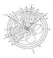
図3は、容器本体14の内部を示す斜視図であり、これ以降、この図3も参照して説明する。真空容器11の内部には、円形のリング状の水平な回転テーブル21が設けられており、この回転テーブル21の表面(一面側)には、当該回転テーブル2の周方向に沿って5つの円形の凹部22が形成されている。この凹部22内に、ウエハWが収納される。つまり、凹部22の底部はウエハWの載置領域として構成される。また、各凹部22には、当該凹部22の底部を貫通する3つの貫通孔22Aが設けられている。 FIG. 3 is a perspective view showing the inside of the
回転テーブル21内周側の縁部は下方に延伸され、垂直な回転円筒部23を構成している(図1参照)。回転円筒部23の下端側は、容器本体14の底部13の中心部に設けられた貫通孔18を介して、当該底部13の下方へ向けて伸び出している。貫通孔18の下方側には、回転円筒部23を囲むように円筒体24が設けられており、円筒体24の上端はOリング25を介して貫通孔18の縁部に接続され、容器本体14に対して固定されている。 An edge on the inner peripheral side of the rotary table 21 extends downward to constitute a vertical rotary cylindrical portion 23 (see FIG. 1). The lower end side of the rotating
上記の回転円筒部23の下端部は、円筒体24よりも下方に延出されており、当該下端部にはベルト26が巻き掛けられている。ベルト26はモータを備えた回転機構27により駆動され、この駆動によって回転円筒部23が軸周りに回転し、回転テーブル21がその周方向に回転する。それによって、凹部22内に収納されたウエハWが回転円筒部23の回転軸を中心に、例えば平面視時計回りに公転する。 A lower end portion of the rotating
容器本体14の底部13の下方には、回転円筒部23の下部、円筒体24、ベルト26及び回転機構27を囲むように、上側が開口したカップ状の底部形成部28が設けられている。この底部形成部28の上端は、容器本体14の底部13の下側に接し、上記の貫通孔18は当該底部形成部28により塞がれている。つまり、この底部形成部28は、容器本体14の中心部における底部を形成している。底部形成部28から円柱状の支柱31が回転円筒部23内を、回転テーブル21の上方へ向かって垂直に伸びており、支柱31の上端は蓋体15の下面の中心部に接し、当該蓋体15を支持している。従って、支柱31は回転テーブル21の回転中心部を上下に貫くように設けられている。支柱31は、例えばアルミニウムなどの金属により構成されている。 Below the
支柱31の下部側は、上部側に比べて拡径された拡径部32を構成している。この拡径部32の外周面と回転円筒部23の内周面との間の隙間、回転円筒部23の外周面と円筒体24の内周面との間の隙間を夫々塞ぐシール部材33、34が設けられている。シール部材33、34は磁性流体シールにより構成され、回転円筒部23が上記のように回転できるように設けられており、これらシール部材33、34により、底部形成部28内に処理空間16に対して区画された空間35が形成される。また、この空間35において、支柱31と回転円筒部23との間に軸受け36が、支柱31と円筒体24との間に軸受け37が夫々設けられている。軸受け36、37により、回転円筒部23が支柱31及び円筒体24に対して支持され、且つ上記のように回転可能に構成される。 The lower side of the
軸受け36、37の他に、上記のベルト26及び回転機構27も空間35に設けられており、この空間35は、底部形成部28に設けられた開口部35Aを介して真空容器11の外部空間と連通している。従って、空間35は大気雰囲気である。開口部35Aはベルト26や回転機構27のメンテナンスを行ったり、真空容器11内の温度変化による空間35の圧力変化を抑えるために設けられている。 In addition to the
また、シール部材33、34は、この例では容器本体14の周縁部側の底部13よりも下方に設けられている。それによって、後述の底部13上に設けられるヒーター54からの熱は、底部13により吸収されることで、シール部材33、34に輻射されることが抑えられる。結果としてシール部材33、34の温度上昇による劣化を抑えることができる。 Further, in this example, the sealing
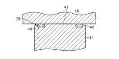
続いて、支柱31の上端部について、図4を参照しながら説明する。図4の上段は、容器本体14から蓋体15が取り外され、容器本体14と蓋体15とが互いに離れた状態を示している。支柱31の上端部には円形の水平な載置面41が形成されている。また、支柱31の上端部には載置面41を囲むように環状の段差部が形成されており、この段差部によって載置面41よりも低い水平なリング状の載置面42が形成されている。載置面42には、当該載置面42に沿って形成された、例えばゴムなどの弾性体により構成されたシール部材であるOリング43が載置されている。つまり、載置面41と載置面42とがなす段差部にOリング43が設けられている。図4に示すように、容器本体14が蓋体15から離れた状態では、載置面42に載置されたOリング43の上端は、載置面41よりも高い。 Then, the upper end part of the support |
蓋体15を容器本体14に装着するために、上記の昇降機構19によって蓋体15を図4の上段に示す状態から下降させると、Oリング43が蓋体15に押し潰されて変形する。そして、当該Oリング43が持つ復元力によって、Oリング43は、蓋体15及び載置面42に密着する。さらに蓋体15が下降すると、載置面41に蓋体15の下面の中心部が当接し、蓋体15が載置面41に載置される。つまり、載置面41は、蓋体15に接触する接触面として構成されている。 When the
図4の中段は、このように蓋体15が載置面42に載置された状態を示しており、点線で囲んだ領域にOリング43の内側付近を拡大して示している。蓋体15と載置面42とが当接することによってパーティクル44が発生しても、Oリング43が蓋体15に密着しているため、この図4中段に示すように、当該パーティクル44の処理空間16への飛散が防がれる。また、Oリング43は支柱31と蓋体15との隙間をシールし、当該隙間において後述のBTBASガスとO3ガスとの接触を防ぐ役割も有する。蓋体15の中心部が載置面42に載置された状態では、蓋体15の周縁部が容器本体14の側壁12の上端に載置された状態となり、図1中に示したように蓋体15が容器本体14に装着された状態となる。この状態で、処理空間16が真空引きされる。 The middle part of FIG. 4 shows a state in which the
この成膜装置1において、支柱31が設けられないとした場合、処理空間16を真空引きしたときに真空容器11の周囲の大気圧によって、蓋体15はその中心部が下方へ押し下げられるように応力を受けて変形するおそれがあり、そのような変形が起きると、ウエハWに所望の膜厚を有する膜を形成できなくなったり、ウエハWの面内の膜厚のばらつきが大きくなってしまうおそれがある。蓋体15の厚さを大きくして蓋体15の強度を高めることで、そのような変形を防ぐことが考えられるが、そうなると蓋体15の重量が増加する。その結果として、昇降機構19の負荷が大きくなってしまい、昇降機構19の大型化ひいては成膜装置1の大型化を招いてしまうおそれがある。しかし、成膜装置1では支柱31により蓋体15の中心部が支持されるため、蓋体15の厚さが大きくなることを抑えながら、蓋体15の変形を抑えることができる。 In this
図1〜図3に戻って説明を続ける。真空容器11の側壁12にはウエハWの搬送口51が開口しており、ゲートバルブ52により開閉自在とされ、図示しないウエハWの搬送機構が搬送口51を介して真空容器11の外部と真空容器11内の処理空間16との間で移動することができる。図1中53は搬送口51を囲むOリングであり、ゲートバルブ52と真空容器11の側壁12との隙間をシールする。 Returning to FIG. 1 to FIG. A
また、真空容器11の底部13には図示しない3本の昇降ピンが設けられ、図示しない昇降機構によって当該昇降ピンの先端が、回転テーブル21の凹部22に設けられる貫通孔22Aを介して、回転テーブル21の下方側と回転テーブル21の上方側との間で昇降自在に構成される。それによって、上記のウエハWの搬送機構と凹部22との間でウエハWの受け渡しが行われる。 In addition, three elevating pins (not shown) are provided on the bottom 13 of the
容器本体14の底部13には、複数のリング状のヒーター54が設けられている。各ヒーター54は、回転テーブル21の回転中心を中心とした同心円状に配置されている。ヒーター54によって、回転テーブル21上のウエハWが加熱される。図中55はヒーターカバーであり、ヒーター54を覆うように設けられる。 A plurality of ring-shaped
容器本体14の底部13においては、ヒーターカバー55の外側に排気口56、57が開口している。排気口56には排気管58の一端が接続され(図1参照)、排気管58の他端は、バルブを含む排気量調整部59を介して真空ポンプにより構成される排気機構50に接続される。図示は省略しているが、排気口57についても排気量調整部59が介設された排気管58の一端が接続され、当該排気口57に接続される排気管58の他端は、排気機構50に接続されている。 At the bottom 13 of the
図3に示すように、回転テーブル21上には、夫々回転テーブル21の外周から中心へ向かって伸びる棒状の第1の処理ガスノズル61、分離ガスノズル62、第2の処理ガスノズル63及び分離ガスノズル64が、この順で周方向に配設されている。これらのガスノズル61〜64は、回転テーブル2の径に沿って設けられた多数の吐出口60を備え、各吐出口60から下方にガスが吐出される。第1の処理ガス供給部である第1の処理ガスノズル61は、BTBAS(ビスターシャルブチルアミノシラン)ガスを吐出し、第2の処理ガス供給部である第2の処理ガスノズル63はO3(オゾン)ガスを吐出する。BTBASガスは、SiO2膜の原料となる原料ガスであり、O3ガスは、原料ガスを酸化する反応ガスである。分離ガスノズル62、64は雰囲気を分離するための分離ガスであるN2(窒素)ガスを吐出する。As shown in FIG. 3, on the
また、前記真空容器11の蓋体15は、下方に突出する平面視扇状の突状部65、66を備えており、突状部65、66は真空容器11の周方向に間隔をおいて形成されている。蓋体15を容器本体14に装着したときには、突状部65、66は支柱31に接すると共に、当該支柱31から回転テーブル21の外側に向かうにつれて、回転テーブル21の周方向に広がるように形成される。突状部65、66は、各々溝67を備えている。溝67は、突状部65、66を周方向に二分割するように形成されており、各溝67に分離ガス供給部である分離ガスノズル62、64が収められる。第1の処理ガスノズル61の下方のガス供給領域を第1の処理領域P1、第2の処理ガスノズル63の下方のガス供給領域を第2の処理領域P2とする。突状部65、67の下方は、分離ガスノズル62、64からのN2ガスが供給される分離領域D、Dとして構成されている。The
上記の排気口56、57の配置について補足して説明しておくと、図2に示すように排気口56、57は、回転テーブル21の外側に設けられており、真空容器11の周方向に時計回りに見て、排気口56は突状部66、突状部65間に開口しており、排気口57は突状部65、突状部66間に開口している。このように開口することで、排気口56はN2ガスと共に第1の処理領域P1に供給されたBTBASガスを排気することができ、排気口57は分離ガスと共に第2の処理領域P2に供給されたO3ガスを排気することができる。 The arrangement of the
図1に示すように、この成膜装置1には、装置全体の動作のコントロールを行うためのコンピュータからなる制御部100が設けられている。この制御部100には、後述のように、ウエハWへの成膜処理を実行するプログラムが格納されている。前記プログラムは、成膜装置1の各部に制御信号を送信して、各部の動作を制御する。 As shown in FIG. 1, the
具体的には、図示しないガス供給源から各ガスノズル61〜64、回転機構27による回転テーブル2の回転速度の制御、排気量調整部59による各排気口56、57からの排気量の調整、昇降ピンの昇降、蓋体15の昇降、ヒーター54への電力供給などの各動作が制御される。前記プログラムにおいては、これらの動作を制御して、後述の各処理が実行されるようにステップ群が組まれている。当該プログラムは、ハードディスク、コンパクトディスク、光磁気ディスク、メモリカード、フレキシブルディスクなどの記憶媒体から制御部100内にインストールされる。 Specifically, each
続いて、成膜装置1による成膜処理について説明する。蓋体15が容器本体14に装着された状態で、ゲートバルブ52が開放され、ウエハWの搬送機構により、真空容器11内にウエハWが順次搬送され、凹部22に受け渡される。続いて、ゲートバルブ52が閉じられ、真空容器11内が、所定の圧力の真空雰囲気になるように排気され、回転テーブル21が回転する。分離ガスノズル62、64からN2ガスが吐出されると共に、第1の処理ガスノズル61からBTBASガスが、第2の処理ガスノズル63からO3ガスが夫々吐出される。 Subsequently, a film forming process performed by the
ウエハWは第1の処理ガスノズル61の下方の第1の処理領域P1と第2の処理ガスノズル63の下方の第2の処理領域P2とを交互に通過し、ウエハWにBTBASガスが吸着され、次いでO3ガスにより吸着されたBTBASガスが酸化されて、酸化シリコンの分子層が1層あるいは複数層形成される。回転テーブル21の回転が続けられ、第1の処理領域P1及び第2の処理領域P2を繰り返しウエハWが通過し、上記の酸化シリコンの分子層が順次積層されて、SiO2膜が形成される。The wafer W alternately passes through the first processing region P1 below the first
図5では矢印により、真空容器11内のガスの流れを示している。分離ガスノズル62、64から前記分離領域Dに供給されたN2ガスが、当該分離領域Dを周方向に広がり、回転テーブル21上を夫々周方向に流れるBTBASガスとO3ガスとが接触することを防ぐ。また、図4の下段に示すように回転テーブル21の中心部においては、支柱31によりBTBASガスとO3ガスとの接触が防がれる。In FIG. 5, the flow of gas in the
所定の回数、回転テーブル21が回転して所定の膜厚のシリコン酸化膜が形成されると、処理ガスノズル61、63から処理ガスの供給及び分離ガスノズル62、64からのN2ガスの供給が停止する。続いて、回転テーブル21の回転が停止し、ゲートバルブ52が開放されて、図示しない搬送機構及び昇降ピンにより、ウエハWが順次真空容器11から搬出され、成膜処理が終了する。When the
真空容器11内のメンテナンスを行う場合は、上記の成膜処理後に昇降機構19により、蓋体15を上昇させ、容器本体17から取り外す。メンテナンス終了後は、図4の上段、中段で説明したように蓋体15を下降させて、容器本体14に装着し、装着後は、後続のウエハWが真空容器11内に搬送され、成膜処理が行われる。 When maintenance is performed in the
この成膜装置1によれば、容器本体14に蓋体15の中心部を支持する支柱31が設けられると共に、蓋体15は当該支柱31及び容器本体14の側壁12に対して分離自在に構成されている。従って、真空容器11内と真空容器11外との圧力差による蓋体15の変形を抑えることができる。また、蓋体15の容器本体14に対する着脱により真空容器11内を開閉自在とし、当該真空容器11内のメンテナンスを容易に行うことができる。ところで、この成膜装置1においては、回転テーブル21上にウエハWを横方向に並べて複数配置するので、平面で見た蓋体15の面積が比較的大きくなり、上記の大気圧と処理空間16との圧力差により蓋体15の中心部に比較的大きな応力が加わりやすいことから、蓋体15の変形を抑えるために上記の支柱31を設けることが特に有効である。 According to the
また、成膜装置1では支柱31が設けられることで、上記のように回転テーブル21の中心部においてBTBASガスとO3ガスとが接触することを防ぎ、その結果としてパーティクルの発生を抑制することができる。支柱31を設けずに、回転テーブル21の中心部にパージガスを供給し、BTBASガスとO3ガスとの接触を抑制することも考えられるが、成膜装置1ではそのような構成に比べて、パージガスによりBTBASガス及びO3ガスが希釈されることがないため、BTBASガス及びO3ガスの使用量を抑えることができる利点がある。Further, the
(第2の実施形態)
第2の実施形態に係る成膜装置7について、図6、図7を参照しながら成膜装置1との差異点を中心に説明する。図6は成膜装置7の縦断側面図であり、図7は成膜装置7の概略横断平面図である。この図7では、図5と同様に、矢印によって成膜処理時の各ガスの流れを示している。(Second Embodiment)
A
成膜装置7においては、容器本体14の底部13に排気口56、57が設けられる代わりに、排気口71、72が支柱31の側面に開口している。真空容器11の周方向に時計回りに見て、排気口71は突状部66、突状部65間に開口しており、排気口72は突状部65、突状部66間に開口している。支柱31内には、排気口71、72に夫々連通する流路73、74が形成されており、流路73、74は支柱31内を垂直方向に設けられる仕切り板75によって互いに区画されている。流路73、74は支柱31の長さ方向に沿って形成され、支柱31内を下方へ向かう途中で合流して、流路76を形成する。流路76は支柱31をさらに下方側に向かうように形成される。 In the
底部形成部28には、排気管58の一端が流路76に開口するように接続されており、排気管58の他端は排気量調整部59を介して排気機構50に接続されている。このような構成によって、排気口71から第1の処理領域P1に供給されたBTBASガスをN2ガスと共に排気し、排気口72から第2の処理領域P2に供給されたO3ガスをN2ガスと共に排気することができる。つまり、排気口71は、BTBASガス及びO3ガスのうちBTBASガスを限定的に排気し、排気口72はBTBASガス及びO3ガスのうちO3ガスを限定的に排気する。上記の仕切り板75は、このように排気が行われる際に、排気口71、72付近でBTBASガスとO3ガスとが接触してパーティクルとなり、処理空間16に飛散してしまうことを防ぐために設けられている。One end of the
この成膜装置7についても成膜装置1と同様の効果が得られる。さらにこの成膜装置7によれば、排気口71、72を支柱31に設けることで、容器本体14に排気口を設ける必要が無くなるため、装置の小型化を図ることができる。 The
ところで、図8に示すように、上記の支柱31において載置面41の周囲に環状の凹部78を形成し、当該凹部78内にOリング43が設けられるようにしていてもよい。凹部78の底面が上記の載置面42を構成する。そして、当該環状の凹部78における内側の側壁の上端面は、蓋体15を載置する載置面41により構成されており、外側の側壁の上端面は載置面41よりも低く形成され、蓋体15に当接しないように構成されている。 By the way, as shown in FIG. 8, an
上記の各成膜装置においては、容器本体14に対して蓋体15が昇降することで、容器本体14に対する蓋体15の着脱が行われるように構成されているが、蓋体15に対して容器本体14が昇降することで、この着脱が行われてもよい。 In each of the above film forming apparatuses, the
また、支柱は容器本体14に設けられることに限られず、蓋体15に設けてもよい。図9は、蓋体15の中心部から下方に伸びるように形成された支柱81を備えた成膜装置1の変形例を示している。この図9の成膜装置1では、シール部材33及び軸受け36が、支柱31と回転円筒部23との隙間に設けられる代わりに、回転円筒部23の内側に起立するように設けられた円筒体82と回転円筒部23との隙間に設けられており、回転円筒部23は支柱31の代わりに当該円筒体82により支持されている。 Further, the support is not limited to being provided on the
蓋体15が容器本体14に装着される際には、蓋体15が下降することで、支柱81の下端部が円筒体82の上方から、当該円筒体82内に進入する。さらに蓋体15が下降して、支柱81の下端が底部形成部28に当接し、支柱81を介して底部形成部28に蓋体15が支持されると共に、容器本体14の側壁12に蓋体15が支持されて、蓋体15が容器本体14に装着される。 When the
図10には、成膜装置1の他の変形例を示している。この図10は、蓋体15に支柱85が設けられ、蓋体15には支柱86が設けられており、蓋体15が容器本体14に装着される際には、支柱85の下端と支柱86の上端とが接し、支柱31と同様の構成の支柱が形成される。つまり、この例では支柱が上下に2分割され、分割された支柱が蓋体15及び容器本体14に夫々設けられている。 FIG. 10 shows another modification of the
(第3の実施形態)
続いて、第3の実施形態に係る成膜装置9について、縦断側面図である図11、概略横断平面図である図12を夫々参照しながら、第2の実施形態の成膜装置7との差異点を中心に説明する。図12では、図7と同様に、矢印によって成膜処理時の各ガスの流れを示している。この成膜装置9に関しては、ガスノズル61、63の構成について成膜装置7と異なっている。(Third embodiment)
Subsequently, with respect to the film forming apparatus 9 according to the third embodiment, referring to FIG. 11 which is a longitudinal side view and FIG. 12 which is a schematic transverse plan view, respectively, with the
この成膜装置9においてもガスノズル61、63は棒状に構成されている。そして、成膜装置9におけるガスノズル61、63の基端は、底部形成部28の下方にて配管58の外側に位置している。このガスノズル61の先端は、排気管58内に向けて水平方向に伸び、排気管58内にて屈曲して流路76、73を上方へ向かった後、さらに屈曲して、排気口71から回転テーブル21の周縁部へ向けて水平に伸びている。また、ガスノズル63の先端は、排気管58内に向けて水平方向に伸び、排気管58内にて屈曲して流路76、74を上方へ向かった後、さらに屈曲して、排気口72から回転テーブル21の周縁部へ向けて水平に伸びている。夫々排気口71、72から突出したガスノズル61、63の各先端部には、吐出口60がガスノズル61、63の伸長方向に多数形成されており、成膜装置1、7と同様に、公転するウエハWの表面全体にBTBASガス及びO3ガスを供給することができる。In this film forming apparatus 9 as well, the
このように成膜装置9においては、支柱31に排気路と、BTBASガスの供給路と、O3ガスの供給路とが互いに区画されて形成されている。このような成膜装置9についても成膜装置7と同様に装置の大きさを抑えることができる。ところで既述の装置の各例の構成は、互いに組み合わせることができる。例えば、成膜装置9について、排気口71、74から排気を行う代わりに、成膜装置1と同様に真空容器14の底部13に排気口56、57を設けて、当該排気口56、57から排気を行うようにしてもよい。As described above, in the film forming apparatus 9, the exhaust path, the BTBAS gas supply path, and the O3 gas supply path are formed in the
また、本発明はウエハWにALDを行う成膜装置に適用されることには限られず、ウエハWに処理ガスを供給して処理する様々な処理装置に適用することができる。例えば、上記の成膜装置1において、分離領域D及び第2の処理ガスノズル63が設けられない構成とし、第1の処理ガスノズル61からは処理ガスを供給してウエハWにCVD(Chemical Vapor Deposition)による成膜が行われる装置とすることができる。また、そのように分離領域D及び第2の処理ガスノズル63を設けない装置構成とした場合、第1の処理ガスノズル61からは不活性ガスを供給することで、ウエハWに形成された膜がアニール処理される装置とすることができる。 In addition, the present invention is not limited to being applied to a film forming apparatus that performs ALD on a wafer W, and can be applied to various processing apparatuses that process by supplying a processing gas to the wafer W. For example, in the
W ウエハ
D 分離領域
P1、P2 処理領域
1 成膜装置
11 真空容器
21 回転テーブル
28 底部形成部
31 支柱
41 載置面
42 載置面
61 第1の処理ガスノズル
62、64 分離ガスノズル
63 第2の処理ガスノズルW Wafer D Separation area P1,
Claims (6)
Translated fromJapanese前記真空容器の底部を含む部分を構成する容器本体と、
前記真空容器を開閉するために前記容器本体に対して分離自在に構成された、当該真空容器の天井部を含む部分を構成する蓋体と、
前記蓋体を容器本体に装着したときに前記回転テーブルの回転中心部を貫くように前記蓋体及び容器本体のうちの一方に設けられ、前記真空容器内を真空引きしたときに前記容器本体に対して蓋体を支持する支柱と、
を備えたことを特徴とする基板処理装置。In the substrate processing apparatus for performing processing by supplying a processing gas to the substrate while revolving the substrate placed on the rotary table in the vacuum vessel,
A container body constituting a portion including the bottom of the vacuum container;
A lid that is configured to be separable from the container body in order to open and close the vacuum container, and that constitutes a portion including a ceiling portion of the vacuum container;
When the lid is attached to the container main body, the lid is provided on one of the lid and the container main body so as to penetrate the rotation center of the rotary table, and when the vacuum container is evacuated, A support column that supports the lid,
A substrate processing apparatus comprising:
前記蓋体を前記容器本体に装着したときに前記蓋体及び容器本体のうちの他方に密着する弾性体からなるシール部材が前記段差部に設けられることを特徴とする請求項1記載の基板処理装置。The column is provided with an annular step portion surrounding a contact surface in contact with the other of the lid and the container body,
2. The substrate processing according to claim 1, wherein a sealing member made of an elastic body that is in close contact with the other of the lid and the container body when the lid is attached to the container body is provided in the step portion. apparatus.
前記第1の処理ガスが供給される第1の処理領域と第2の処理ガスが供給される第2の処理領域との雰囲気を分離するために前記回転方向においてこれら処理領域の間に設けられ、分離ガス供給部から分離ガスを供給するための分離領域と、を備え、
前記排気口は互いに区画された第1の排気口と第2の排気口とにより構成され、
前記第1の排気口は、第1の処理ガス及び第2の処理ガスのうちの一方を限定的に排気し、第2の排気口は第1の処理ガス及び第2の処理ガスのうちの他方を限定的に排気することを特徴とする請求項3記載の基板処理装置。A first processing gas supply unit and a second processing gas supply unit, which are provided apart from each other in the rotation direction of the turntable and supply a first processing gas and a second processing gas to the substrate, respectively;
In order to separate the atmosphere of the first processing region to which the first processing gas is supplied and the second processing region to which the second processing gas is supplied, provided between the processing regions in the rotation direction. A separation region for supplying separation gas from the separation gas supply unit,
The exhaust port is constituted by a first exhaust port and a second exhaust port that are partitioned from each other;
The first exhaust port exhausts one of the first process gas and the second process gas in a limited manner, and the second exhaust port includes one of the first process gas and the second process gas. 4. The substrate processing apparatus according to claim 3, wherein the other is exhausted in a limited manner.
Priority Applications (4)
| Application Number | Priority Date | Filing Date | Title |
|---|---|---|---|
| JP2015020536AJP6398761B2 (en) | 2015-02-04 | 2015-02-04 | Substrate processing equipment |
| US15/007,488US9683290B2 (en) | 2015-02-04 | 2016-01-27 | Substrate processing apparatus having a pillar support structure for preventing transformation of a ceiling portion |
| KR1020160012346AKR102003108B1 (en) | 2015-02-04 | 2016-02-01 | Substrate processing apparatus |
| TW105103221ATWI673793B (en) | 2015-02-04 | 2016-02-02 | Substrate processing apparatus |
Applications Claiming Priority (1)
| Application Number | Priority Date | Filing Date | Title |
|---|---|---|---|
| JP2015020536AJP6398761B2 (en) | 2015-02-04 | 2015-02-04 | Substrate processing equipment |
Publications (2)
| Publication Number | Publication Date |
|---|---|
| JP2016143836Atrue JP2016143836A (en) | 2016-08-08 |
| JP6398761B2 JP6398761B2 (en) | 2018-10-03 |
Family
ID=56553915
Family Applications (1)
| Application Number | Title | Priority Date | Filing Date |
|---|---|---|---|
| JP2015020536AActiveJP6398761B2 (en) | 2015-02-04 | 2015-02-04 | Substrate processing equipment |
Country Status (4)
| Country | Link |
|---|---|
| US (1) | US9683290B2 (en) |
| JP (1) | JP6398761B2 (en) |
| KR (1) | KR102003108B1 (en) |
| TW (1) | TWI673793B (en) |
Cited By (1)
| Publication number | Priority date | Publication date | Assignee | Title |
|---|---|---|---|---|
| JP7666234B2 (en) | 2021-08-27 | 2025-04-22 | 東京エレクトロン株式会社 | Apparatus for performing film formation process on substrate and method for exhausting process gas from the apparatus for performing film formation process on substrate |
Families Citing this family (279)
| Publication number | Priority date | Publication date | Assignee | Title |
|---|---|---|---|---|
| US20130023129A1 (en) | 2011-07-20 | 2013-01-24 | Asm America, Inc. | Pressure transmitter for a semiconductor processing environment |
| US10714315B2 (en) | 2012-10-12 | 2020-07-14 | Asm Ip Holdings B.V. | Semiconductor reaction chamber showerhead |
| US20160376700A1 (en) | 2013-02-01 | 2016-12-29 | Asm Ip Holding B.V. | System for treatment of deposition reactor |
| US11015245B2 (en) | 2014-03-19 | 2021-05-25 | Asm Ip Holding B.V. | Gas-phase reactor and system having exhaust plenum and components thereof |
| US10941490B2 (en) | 2014-10-07 | 2021-03-09 | Asm Ip Holding B.V. | Multiple temperature range susceptor, assembly, reactor and system including the susceptor, and methods of using the same |
| JP6398761B2 (en)* | 2015-02-04 | 2018-10-03 | 東京エレクトロン株式会社 | Substrate processing equipment |
| US10276355B2 (en) | 2015-03-12 | 2019-04-30 | Asm Ip Holding B.V. | Multi-zone reactor, system including the reactor, and method of using the same |
| US10458018B2 (en) | 2015-06-26 | 2019-10-29 | Asm Ip Holding B.V. | Structures including metal carbide material, devices including the structures, and methods of forming same |
| US10211308B2 (en) | 2015-10-21 | 2019-02-19 | Asm Ip Holding B.V. | NbMC layers |
| US11139308B2 (en) | 2015-12-29 | 2021-10-05 | Asm Ip Holding B.V. | Atomic layer deposition of III-V compounds to form V-NAND devices |
| US10529554B2 (en) | 2016-02-19 | 2020-01-07 | Asm Ip Holding B.V. | Method for forming silicon nitride film selectively on sidewalls or flat surfaces of trenches |
| US10343920B2 (en) | 2016-03-18 | 2019-07-09 | Asm Ip Holding B.V. | Aligned carbon nanotubes |
| US10367080B2 (en) | 2016-05-02 | 2019-07-30 | Asm Ip Holding B.V. | Method of forming a germanium oxynitride film |
| US11453943B2 (en) | 2016-05-25 | 2022-09-27 | Asm Ip Holding B.V. | Method for forming carbon-containing silicon/metal oxide or nitride film by ALD using silicon precursor and hydrocarbon precursor |
| US9859151B1 (en) | 2016-07-08 | 2018-01-02 | Asm Ip Holding B.V. | Selective film deposition method to form air gaps |
| US10612137B2 (en) | 2016-07-08 | 2020-04-07 | Asm Ip Holdings B.V. | Organic reactants for atomic layer deposition |
| US9887082B1 (en) | 2016-07-28 | 2018-02-06 | Asm Ip Holding B.V. | Method and apparatus for filling a gap |
| US9812320B1 (en) | 2016-07-28 | 2017-11-07 | Asm Ip Holding B.V. | Method and apparatus for filling a gap |
| KR102532607B1 (en) | 2016-07-28 | 2023-05-15 | 에이에스엠 아이피 홀딩 비.브이. | Substrate processing apparatus and method of operating the same |
| US11532757B2 (en) | 2016-10-27 | 2022-12-20 | Asm Ip Holding B.V. | Deposition of charge trapping layers |
| US10714350B2 (en) | 2016-11-01 | 2020-07-14 | ASM IP Holdings, B.V. | Methods for forming a transition metal niobium nitride film on a substrate by atomic layer deposition and related semiconductor device structures |
| KR102546317B1 (en) | 2016-11-15 | 2023-06-21 | 에이에스엠 아이피 홀딩 비.브이. | Gas supply unit and substrate processing apparatus including the same |
| KR102762543B1 (en) | 2016-12-14 | 2025-02-05 | 에이에스엠 아이피 홀딩 비.브이. | Substrate processing apparatus |
| US11581186B2 (en) | 2016-12-15 | 2023-02-14 | Asm Ip Holding B.V. | Sequential infiltration synthesis apparatus |
| US11447861B2 (en) | 2016-12-15 | 2022-09-20 | Asm Ip Holding B.V. | Sequential infiltration synthesis apparatus and a method of forming a patterned structure |
| KR102700194B1 (en) | 2016-12-19 | 2024-08-28 | 에이에스엠 아이피 홀딩 비.브이. | Substrate processing apparatus |
| US10269558B2 (en) | 2016-12-22 | 2019-04-23 | Asm Ip Holding B.V. | Method of forming a structure on a substrate |
| US11390950B2 (en) | 2017-01-10 | 2022-07-19 | Asm Ip Holding B.V. | Reactor system and method to reduce residue buildup during a film deposition process |
| US10468261B2 (en) | 2017-02-15 | 2019-11-05 | Asm Ip Holding B.V. | Methods for forming a metallic film on a substrate by cyclical deposition and related semiconductor device structures |
| US10529563B2 (en) | 2017-03-29 | 2020-01-07 | Asm Ip Holdings B.V. | Method for forming doped metal oxide films on a substrate by cyclical deposition and related semiconductor device structures |
| US10770286B2 (en) | 2017-05-08 | 2020-09-08 | Asm Ip Holdings B.V. | Methods for selectively forming a silicon nitride film on a substrate and related semiconductor device structures |
| US12040200B2 (en) | 2017-06-20 | 2024-07-16 | Asm Ip Holding B.V. | Semiconductor processing apparatus and methods for calibrating a semiconductor processing apparatus |
| US11306395B2 (en) | 2017-06-28 | 2022-04-19 | Asm Ip Holding B.V. | Methods for depositing a transition metal nitride film on a substrate by atomic layer deposition and related deposition apparatus |
| KR20190009245A (en) | 2017-07-18 | 2019-01-28 | 에이에스엠 아이피 홀딩 비.브이. | Methods for forming a semiconductor device structure and related semiconductor device structures |
| US11374112B2 (en) | 2017-07-19 | 2022-06-28 | Asm Ip Holding B.V. | Method for depositing a group IV semiconductor and related semiconductor device structures |
| US10541333B2 (en) | 2017-07-19 | 2020-01-21 | Asm Ip Holding B.V. | Method for depositing a group IV semiconductor and related semiconductor device structures |
| US11018002B2 (en) | 2017-07-19 | 2021-05-25 | Asm Ip Holding B.V. | Method for selectively depositing a Group IV semiconductor and related semiconductor device structures |
| US10590535B2 (en) | 2017-07-26 | 2020-03-17 | Asm Ip Holdings B.V. | Chemical treatment, deposition and/or infiltration apparatus and method for using the same |
| KR102481410B1 (en)* | 2017-07-31 | 2022-12-26 | 에이에스엠 아이피 홀딩 비.브이. | Substrate processing apparatus |
| TWI815813B (en) | 2017-08-04 | 2023-09-21 | 荷蘭商Asm智慧財產控股公司 | Showerhead assembly for distributing a gas within a reaction chamber |
| US10770336B2 (en) | 2017-08-08 | 2020-09-08 | Asm Ip Holding B.V. | Substrate lift mechanism and reactor including same |
| US10692741B2 (en) | 2017-08-08 | 2020-06-23 | Asm Ip Holdings B.V. | Radiation shield |
| US11769682B2 (en) | 2017-08-09 | 2023-09-26 | Asm Ip Holding B.V. | Storage apparatus for storing cassettes for substrates and processing apparatus equipped therewith |
| US11139191B2 (en) | 2017-08-09 | 2021-10-05 | Asm Ip Holding B.V. | Storage apparatus for storing cassettes for substrates and processing apparatus equipped therewith |
| US11830730B2 (en) | 2017-08-29 | 2023-11-28 | Asm Ip Holding B.V. | Layer forming method and apparatus |
| US11056344B2 (en) | 2017-08-30 | 2021-07-06 | Asm Ip Holding B.V. | Layer forming method |
| KR102491945B1 (en) | 2017-08-30 | 2023-01-26 | 에이에스엠 아이피 홀딩 비.브이. | Substrate processing apparatus |
| US11295980B2 (en) | 2017-08-30 | 2022-04-05 | Asm Ip Holding B.V. | Methods for depositing a molybdenum metal film over a dielectric surface of a substrate by a cyclical deposition process and related semiconductor device structures |
| US10658205B2 (en) | 2017-09-28 | 2020-05-19 | Asm Ip Holdings B.V. | Chemical dispensing apparatus and methods for dispensing a chemical to a reaction chamber |
| US10403504B2 (en) | 2017-10-05 | 2019-09-03 | Asm Ip Holding B.V. | Method for selectively depositing a metallic film on a substrate |
| US10923344B2 (en) | 2017-10-30 | 2021-02-16 | Asm Ip Holding B.V. | Methods for forming a semiconductor structure and related semiconductor structures |
| US11022879B2 (en) | 2017-11-24 | 2021-06-01 | Asm Ip Holding B.V. | Method of forming an enhanced unexposed photoresist layer |
| WO2019103613A1 (en) | 2017-11-27 | 2019-05-31 | Asm Ip Holding B.V. | A storage device for storing wafer cassettes for use with a batch furnace |
| CN111344522B (en) | 2017-11-27 | 2022-04-12 | 阿斯莫Ip控股公司 | Including clean mini-environment device |
| JP6906439B2 (en)* | 2017-12-21 | 2021-07-21 | 東京エレクトロン株式会社 | Film formation method |
| US10872771B2 (en) | 2018-01-16 | 2020-12-22 | Asm Ip Holding B. V. | Method for depositing a material film on a substrate within a reaction chamber by a cyclical deposition process and related device structures |
| TWI799494B (en) | 2018-01-19 | 2023-04-21 | 荷蘭商Asm 智慧財產控股公司 | Deposition method |
| KR102695659B1 (en) | 2018-01-19 | 2024-08-14 | 에이에스엠 아이피 홀딩 비.브이. | Method for depositing a gap filling layer by plasma assisted deposition |
| US11081345B2 (en) | 2018-02-06 | 2021-08-03 | Asm Ip Holding B.V. | Method of post-deposition treatment for silicon oxide film |
| US10896820B2 (en) | 2018-02-14 | 2021-01-19 | Asm Ip Holding B.V. | Method for depositing a ruthenium-containing film on a substrate by a cyclical deposition process |
| WO2019158960A1 (en) | 2018-02-14 | 2019-08-22 | Asm Ip Holding B.V. | A method for depositing a ruthenium-containing film on a substrate by a cyclical deposition process |
| US10731249B2 (en) | 2018-02-15 | 2020-08-04 | Asm Ip Holding B.V. | Method of forming a transition metal containing film on a substrate by a cyclical deposition process, a method for supplying a transition metal halide compound to a reaction chamber, and related vapor deposition apparatus |
| KR102636427B1 (en) | 2018-02-20 | 2024-02-13 | 에이에스엠 아이피 홀딩 비.브이. | Substrate processing method and apparatus |
| US10975470B2 (en) | 2018-02-23 | 2021-04-13 | Asm Ip Holding B.V. | Apparatus for detecting or monitoring for a chemical precursor in a high temperature environment |
| US11473195B2 (en) | 2018-03-01 | 2022-10-18 | Asm Ip Holding B.V. | Semiconductor processing apparatus and a method for processing a substrate |
| US11629406B2 (en) | 2018-03-09 | 2023-04-18 | Asm Ip Holding B.V. | Semiconductor processing apparatus comprising one or more pyrometers for measuring a temperature of a substrate during transfer of the substrate |
| US11114283B2 (en) | 2018-03-16 | 2021-09-07 | Asm Ip Holding B.V. | Reactor, system including the reactor, and methods of manufacturing and using same |
| KR102646467B1 (en) | 2018-03-27 | 2024-03-11 | 에이에스엠 아이피 홀딩 비.브이. | Method of forming an electrode on a substrate and a semiconductor device structure including an electrode |
| US11230766B2 (en) | 2018-03-29 | 2022-01-25 | Asm Ip Holding B.V. | Substrate processing apparatus and method |
| US11088002B2 (en) | 2018-03-29 | 2021-08-10 | Asm Ip Holding B.V. | Substrate rack and a substrate processing system and method |
| KR102600229B1 (en) | 2018-04-09 | 2023-11-10 | 에이에스엠 아이피 홀딩 비.브이. | Substrate supporting device, substrate processing apparatus including the same and substrate processing method |
| US12025484B2 (en) | 2018-05-08 | 2024-07-02 | Asm Ip Holding B.V. | Thin film forming method |
| TWI811348B (en) | 2018-05-08 | 2023-08-11 | 荷蘭商Asm 智慧財產控股公司 | Methods for depositing an oxide film on a substrate by a cyclical deposition process and related device structures |
| US12272527B2 (en) | 2018-05-09 | 2025-04-08 | Asm Ip Holding B.V. | Apparatus for use with hydrogen radicals and method of using same |
| KR102596988B1 (en) | 2018-05-28 | 2023-10-31 | 에이에스엠 아이피 홀딩 비.브이. | Method of processing a substrate and a device manufactured by the same |
| TWI840362B (en) | 2018-06-04 | 2024-05-01 | 荷蘭商Asm Ip私人控股有限公司 | Wafer handling chamber with moisture reduction |
| US11718913B2 (en) | 2018-06-04 | 2023-08-08 | Asm Ip Holding B.V. | Gas distribution system and reactor system including same |
| US11286562B2 (en) | 2018-06-08 | 2022-03-29 | Asm Ip Holding B.V. | Gas-phase chemical reactor and method of using same |
| US10797133B2 (en) | 2018-06-21 | 2020-10-06 | Asm Ip Holding B.V. | Method for depositing a phosphorus doped silicon arsenide film and related semiconductor device structures |
| KR102568797B1 (en) | 2018-06-21 | 2023-08-21 | 에이에스엠 아이피 홀딩 비.브이. | Substrate processing system |
| KR102854019B1 (en) | 2018-06-27 | 2025-09-02 | 에이에스엠 아이피 홀딩 비.브이. | Periodic deposition method for forming a metal-containing material and films and structures comprising the metal-containing material |
| TWI873894B (en) | 2018-06-27 | 2025-02-21 | 荷蘭商Asm Ip私人控股有限公司 | Cyclic deposition methods for forming metal-containing material and films and structures including the metal-containing material |
| US10612136B2 (en) | 2018-06-29 | 2020-04-07 | ASM IP Holding, B.V. | Temperature-controlled flange and reactor system including same |
| US10388513B1 (en) | 2018-07-03 | 2019-08-20 | Asm Ip Holding B.V. | Method for depositing silicon-free carbon-containing film as gap-fill layer by pulse plasma-assisted deposition |
| US10755922B2 (en) | 2018-07-03 | 2020-08-25 | Asm Ip Holding B.V. | Method for depositing silicon-free carbon-containing film as gap-fill layer by pulse plasma-assisted deposition |
| US11053591B2 (en) | 2018-08-06 | 2021-07-06 | Asm Ip Holding B.V. | Multi-port gas injection system and reactor system including same |
| US11430674B2 (en) | 2018-08-22 | 2022-08-30 | Asm Ip Holding B.V. | Sensor array, apparatus for dispensing a vapor phase reactant to a reaction chamber and related methods |
| KR102707956B1 (en) | 2018-09-11 | 2024-09-19 | 에이에스엠 아이피 홀딩 비.브이. | Method for deposition of a thin film |
| US11024523B2 (en) | 2018-09-11 | 2021-06-01 | Asm Ip Holding B.V. | Substrate processing apparatus and method |
| US11049751B2 (en) | 2018-09-14 | 2021-06-29 | Asm Ip Holding B.V. | Cassette supply system to store and handle cassettes and processing apparatus equipped therewith |
| CN110970344B (en) | 2018-10-01 | 2024-10-25 | Asmip控股有限公司 | Substrate holding apparatus, system comprising the same and method of using the same |
| US11232963B2 (en) | 2018-10-03 | 2022-01-25 | Asm Ip Holding B.V. | Substrate processing apparatus and method |
| KR102592699B1 (en) | 2018-10-08 | 2023-10-23 | 에이에스엠 아이피 홀딩 비.브이. | Substrate support unit and apparatuses for depositing thin film and processing the substrate including the same |
| KR102546322B1 (en) | 2018-10-19 | 2023-06-21 | 에이에스엠 아이피 홀딩 비.브이. | Substrate processing apparatus and substrate processing method |
| KR102605121B1 (en) | 2018-10-19 | 2023-11-23 | 에이에스엠 아이피 홀딩 비.브이. | Substrate processing apparatus and substrate processing method |
| USD948463S1 (en) | 2018-10-24 | 2022-04-12 | Asm Ip Holding B.V. | Susceptor for semiconductor substrate supporting apparatus |
| US12378665B2 (en) | 2018-10-26 | 2025-08-05 | Asm Ip Holding B.V. | High temperature coatings for a preclean and etch apparatus and related methods |
| US11087997B2 (en) | 2018-10-31 | 2021-08-10 | Asm Ip Holding B.V. | Substrate processing apparatus for processing substrates |
| KR102748291B1 (en) | 2018-11-02 | 2024-12-31 | 에이에스엠 아이피 홀딩 비.브이. | Substrate support unit and substrate processing apparatus including the same |
| US11572620B2 (en) | 2018-11-06 | 2023-02-07 | Asm Ip Holding B.V. | Methods for selectively depositing an amorphous silicon film on a substrate |
| US11031242B2 (en) | 2018-11-07 | 2021-06-08 | Asm Ip Holding B.V. | Methods for depositing a boron doped silicon germanium film |
| US10818758B2 (en) | 2018-11-16 | 2020-10-27 | Asm Ip Holding B.V. | Methods for forming a metal silicate film on a substrate in a reaction chamber and related semiconductor device structures |
| US10847366B2 (en) | 2018-11-16 | 2020-11-24 | Asm Ip Holding B.V. | Methods for depositing a transition metal chalcogenide film on a substrate by a cyclical deposition process |
| US12040199B2 (en) | 2018-11-28 | 2024-07-16 | Asm Ip Holding B.V. | Substrate processing apparatus for processing substrates |
| US11217444B2 (en) | 2018-11-30 | 2022-01-04 | Asm Ip Holding B.V. | Method for forming an ultraviolet radiation responsive metal oxide-containing film |
| KR102636428B1 (en) | 2018-12-04 | 2024-02-13 | 에이에스엠 아이피 홀딩 비.브이. | A method for cleaning a substrate processing apparatus |
| US11158513B2 (en) | 2018-12-13 | 2021-10-26 | Asm Ip Holding B.V. | Methods for forming a rhenium-containing film on a substrate by a cyclical deposition process and related semiconductor device structures |
| TWI874340B (en) | 2018-12-14 | 2025-03-01 | 荷蘭商Asm Ip私人控股有限公司 | Method of forming device structure, structure formed by the method and system for performing the method |
| TWI866480B (en) | 2019-01-17 | 2024-12-11 | 荷蘭商Asm Ip 私人控股有限公司 | Methods of forming a transition metal containing film on a substrate by a cyclical deposition process |
| KR102727227B1 (en) | 2019-01-22 | 2024-11-07 | 에이에스엠 아이피 홀딩 비.브이. | Semiconductor processing device |
| CN111524788B (en) | 2019-02-01 | 2023-11-24 | Asm Ip私人控股有限公司 | Method for forming topologically selective films of silicon oxide |
| TWI845607B (en) | 2019-02-20 | 2024-06-21 | 荷蘭商Asm Ip私人控股有限公司 | Cyclical deposition method and apparatus for filling a recess formed within a substrate surface |
| KR102626263B1 (en) | 2019-02-20 | 2024-01-16 | 에이에스엠 아이피 홀딩 비.브이. | Cyclical deposition method including treatment step and apparatus for same |
| TWI873122B (en) | 2019-02-20 | 2025-02-21 | 荷蘭商Asm Ip私人控股有限公司 | Method of filling a recess formed within a surface of a substrate, semiconductor structure formed according to the method, and semiconductor processing apparatus |
| TWI838458B (en) | 2019-02-20 | 2024-04-11 | 荷蘭商Asm Ip私人控股有限公司 | Apparatus and methods for plug fill deposition in 3-d nand applications |
| TWI842826B (en) | 2019-02-22 | 2024-05-21 | 荷蘭商Asm Ip私人控股有限公司 | Substrate processing apparatus and method for processing substrate |
| KR102782593B1 (en) | 2019-03-08 | 2025-03-14 | 에이에스엠 아이피 홀딩 비.브이. | Structure Including SiOC Layer and Method of Forming Same |
| KR102858005B1 (en) | 2019-03-08 | 2025-09-09 | 에이에스엠 아이피 홀딩 비.브이. | Method for Selective Deposition of Silicon Nitride Layer and Structure Including Selectively-Deposited Silicon Nitride Layer |
| US11742198B2 (en) | 2019-03-08 | 2023-08-29 | Asm Ip Holding B.V. | Structure including SiOCN layer and method of forming same |
| JP2020167398A (en) | 2019-03-28 | 2020-10-08 | エーエスエム・アイピー・ホールディング・ベー・フェー | Door openers and substrate processing equipment provided with door openers |
| KR102809999B1 (en) | 2019-04-01 | 2025-05-19 | 에이에스엠 아이피 홀딩 비.브이. | Method of manufacturing semiconductor device |
| KR20200123380A (en) | 2019-04-19 | 2020-10-29 | 에이에스엠 아이피 홀딩 비.브이. | Layer forming method and apparatus |
| KR20200125453A (en) | 2019-04-24 | 2020-11-04 | 에이에스엠 아이피 홀딩 비.브이. | Gas-phase reactor system and method of using same |
| US11289326B2 (en) | 2019-05-07 | 2022-03-29 | Asm Ip Holding B.V. | Method for reforming amorphous carbon polymer film |
| KR20200130121A (en) | 2019-05-07 | 2020-11-18 | 에이에스엠 아이피 홀딩 비.브이. | Chemical source vessel with dip tube |
| KR20200130652A (en) | 2019-05-10 | 2020-11-19 | 에이에스엠 아이피 홀딩 비.브이. | Method of depositing material onto a surface and structure formed according to the method |
| JP7612342B2 (en) | 2019-05-16 | 2025-01-14 | エーエスエム・アイピー・ホールディング・ベー・フェー | Wafer boat handling apparatus, vertical batch furnace and method |
| JP7598201B2 (en) | 2019-05-16 | 2024-12-11 | エーエスエム・アイピー・ホールディング・ベー・フェー | Wafer boat handling apparatus, vertical batch furnace and method |
| USD975665S1 (en) | 2019-05-17 | 2023-01-17 | Asm Ip Holding B.V. | Susceptor shaft |
| USD947913S1 (en) | 2019-05-17 | 2022-04-05 | Asm Ip Holding B.V. | Susceptor shaft |
| USD935572S1 (en) | 2019-05-24 | 2021-11-09 | Asm Ip Holding B.V. | Gas channel plate |
| USD922229S1 (en) | 2019-06-05 | 2021-06-15 | Asm Ip Holding B.V. | Device for controlling a temperature of a gas supply unit |
| KR20200141002A (en) | 2019-06-06 | 2020-12-17 | 에이에스엠 아이피 홀딩 비.브이. | Method of using a gas-phase reactor system including analyzing exhausted gas |
| KR20200141931A (en) | 2019-06-10 | 2020-12-21 | 에이에스엠 아이피 홀딩 비.브이. | Method for cleaning quartz epitaxial chambers |
| KR20200143254A (en) | 2019-06-11 | 2020-12-23 | 에이에스엠 아이피 홀딩 비.브이. | Method of forming an electronic structure using an reforming gas, system for performing the method, and structure formed using the method |
| USD944946S1 (en) | 2019-06-14 | 2022-03-01 | Asm Ip Holding B.V. | Shower plate |
| USD931978S1 (en) | 2019-06-27 | 2021-09-28 | Asm Ip Holding B.V. | Showerhead vacuum transport |
| KR20210005515A (en) | 2019-07-03 | 2021-01-14 | 에이에스엠 아이피 홀딩 비.브이. | Temperature control assembly for substrate processing apparatus and method of using same |
| JP7499079B2 (en) | 2019-07-09 | 2024-06-13 | エーエスエム・アイピー・ホールディング・ベー・フェー | Plasma device using coaxial waveguide and substrate processing method |
| CN112216646A (en) | 2019-07-10 | 2021-01-12 | Asm Ip私人控股有限公司 | Substrate supporting assembly and substrate processing device comprising same |
| KR20210010307A (en) | 2019-07-16 | 2021-01-27 | 에이에스엠 아이피 홀딩 비.브이. | Substrate processing apparatus |
| KR102860110B1 (en) | 2019-07-17 | 2025-09-16 | 에이에스엠 아이피 홀딩 비.브이. | Methods of forming silicon germanium structures |
| KR20210010816A (en) | 2019-07-17 | 2021-01-28 | 에이에스엠 아이피 홀딩 비.브이. | Radical assist ignition plasma system and method |
| US11643724B2 (en) | 2019-07-18 | 2023-05-09 | Asm Ip Holding B.V. | Method of forming structures using a neutral beam |
| KR20210010817A (en) | 2019-07-19 | 2021-01-28 | 에이에스엠 아이피 홀딩 비.브이. | Method of Forming Topology-Controlled Amorphous Carbon Polymer Film |
| TWI839544B (en) | 2019-07-19 | 2024-04-21 | 荷蘭商Asm Ip私人控股有限公司 | Method of forming topology-controlled amorphous carbon polymer film |
| TWI851767B (en) | 2019-07-29 | 2024-08-11 | 荷蘭商Asm Ip私人控股有限公司 | Methods for selective deposition utilizing n-type dopants and/or alternative dopants to achieve high dopant incorporation |
| CN112309899A (en) | 2019-07-30 | 2021-02-02 | Asm Ip私人控股有限公司 | Substrate processing apparatus |
| CN112309900A (en) | 2019-07-30 | 2021-02-02 | Asm Ip私人控股有限公司 | Substrate processing apparatus |
| US12169361B2 (en) | 2019-07-30 | 2024-12-17 | Asm Ip Holding B.V. | Substrate processing apparatus and method |
| US11587814B2 (en) | 2019-07-31 | 2023-02-21 | Asm Ip Holding B.V. | Vertical batch furnace assembly |
| US11587815B2 (en) | 2019-07-31 | 2023-02-21 | Asm Ip Holding B.V. | Vertical batch furnace assembly |
| US11227782B2 (en) | 2019-07-31 | 2022-01-18 | Asm Ip Holding B.V. | Vertical batch furnace assembly |
| CN112323048B (en) | 2019-08-05 | 2024-02-09 | Asm Ip私人控股有限公司 | Liquid level sensor for chemical source container |
| CN112342526A (en) | 2019-08-09 | 2021-02-09 | Asm Ip私人控股有限公司 | Heater assembly including cooling device and method of using same |
| US11631571B2 (en) | 2019-08-12 | 2023-04-18 | Kurt J. Lesker Company | Ultra high purity conditions for atomic scale processing |
| USD965524S1 (en) | 2019-08-19 | 2022-10-04 | Asm Ip Holding B.V. | Susceptor support |
| USD965044S1 (en) | 2019-08-19 | 2022-09-27 | Asm Ip Holding B.V. | Susceptor shaft |
| JP2021031769A (en) | 2019-08-21 | 2021-03-01 | エーエスエム アイピー ホールディング ビー.ブイ. | Production apparatus of mixed gas of film deposition raw material and film deposition apparatus |
| USD930782S1 (en) | 2019-08-22 | 2021-09-14 | Asm Ip Holding B.V. | Gas distributor |
| USD949319S1 (en) | 2019-08-22 | 2022-04-19 | Asm Ip Holding B.V. | Exhaust duct |
| KR20210024423A (en) | 2019-08-22 | 2021-03-05 | 에이에스엠 아이피 홀딩 비.브이. | Method for forming a structure with a hole |
| USD979506S1 (en) | 2019-08-22 | 2023-02-28 | Asm Ip Holding B.V. | Insulator |
| USD940837S1 (en) | 2019-08-22 | 2022-01-11 | Asm Ip Holding B.V. | Electrode |
| KR20210024420A (en) | 2019-08-23 | 2021-03-05 | 에이에스엠 아이피 홀딩 비.브이. | Method for depositing silicon oxide film having improved quality by peald using bis(diethylamino)silane |
| US11286558B2 (en) | 2019-08-23 | 2022-03-29 | Asm Ip Holding B.V. | Methods for depositing a molybdenum nitride film on a surface of a substrate by a cyclical deposition process and related semiconductor device structures including a molybdenum nitride film |
| KR102806450B1 (en) | 2019-09-04 | 2025-05-12 | 에이에스엠 아이피 홀딩 비.브이. | Methods for selective deposition using a sacrificial capping layer |
| KR102733104B1 (en) | 2019-09-05 | 2024-11-22 | 에이에스엠 아이피 홀딩 비.브이. | Substrate processing apparatus |
| US20220336194A1 (en)* | 2019-09-17 | 2022-10-20 | Tokyo Electron Limited | Plasma processing apparatus |
| US11562901B2 (en) | 2019-09-25 | 2023-01-24 | Asm Ip Holding B.V. | Substrate processing method |
| CN112593212B (en) | 2019-10-02 | 2023-12-22 | Asm Ip私人控股有限公司 | Method for forming topologically selective silicon oxide film by cyclic plasma enhanced deposition process |
| TW202128273A (en) | 2019-10-08 | 2021-08-01 | 荷蘭商Asm Ip私人控股有限公司 | Gas injection system, reactor system, and method of depositing material on surface of substratewithin reaction chamber |
| KR20210042810A (en) | 2019-10-08 | 2021-04-20 | 에이에스엠 아이피 홀딩 비.브이. | Reactor system including a gas distribution assembly for use with activated species and method of using same |
| TWI846953B (en) | 2019-10-08 | 2024-07-01 | 荷蘭商Asm Ip私人控股有限公司 | Substrate processing device |
| TWI846966B (en) | 2019-10-10 | 2024-07-01 | 荷蘭商Asm Ip私人控股有限公司 | Method of forming a photoresist underlayer and structure including same |
| US12009241B2 (en) | 2019-10-14 | 2024-06-11 | Asm Ip Holding B.V. | Vertical batch furnace assembly with detector to detect cassette |
| TWI834919B (en) | 2019-10-16 | 2024-03-11 | 荷蘭商Asm Ip私人控股有限公司 | Method of topology-selective film formation of silicon oxide |
| US11637014B2 (en) | 2019-10-17 | 2023-04-25 | Asm Ip Holding B.V. | Methods for selective deposition of doped semiconductor material |
| KR102845724B1 (en) | 2019-10-21 | 2025-08-13 | 에이에스엠 아이피 홀딩 비.브이. | Apparatus and methods for selectively etching films |
| KR20210050453A (en) | 2019-10-25 | 2021-05-07 | 에이에스엠 아이피 홀딩 비.브이. | Methods for filling a gap feature on a substrate surface and related semiconductor structures |
| US11646205B2 (en) | 2019-10-29 | 2023-05-09 | Asm Ip Holding B.V. | Methods of selectively forming n-type doped material on a surface, systems for selectively forming n-type doped material, and structures formed using same |
| KR20210054983A (en) | 2019-11-05 | 2021-05-14 | 에이에스엠 아이피 홀딩 비.브이. | Structures with doped semiconductor layers and methods and systems for forming same |
| US11501968B2 (en) | 2019-11-15 | 2022-11-15 | Asm Ip Holding B.V. | Method for providing a semiconductor device with silicon filled gaps |
| KR102861314B1 (en) | 2019-11-20 | 2025-09-17 | 에이에스엠 아이피 홀딩 비.브이. | Method of depositing carbon-containing material on a surface of a substrate, structure formed using the method, and system for forming the structure |
| US11450529B2 (en) | 2019-11-26 | 2022-09-20 | Asm Ip Holding B.V. | Methods for selectively forming a target film on a substrate comprising a first dielectric surface and a second metallic surface |
| CN112951697B (en) | 2019-11-26 | 2025-07-29 | Asmip私人控股有限公司 | Substrate processing apparatus |
| CN120432376A (en) | 2019-11-29 | 2025-08-05 | Asm Ip私人控股有限公司 | Substrate processing apparatus |
| CN112885692B (en) | 2019-11-29 | 2025-08-15 | Asmip私人控股有限公司 | Substrate processing apparatus |
| JP7527928B2 (en) | 2019-12-02 | 2024-08-05 | エーエスエム・アイピー・ホールディング・ベー・フェー | Substrate processing apparatus and substrate processing method |
| KR20210070898A (en) | 2019-12-04 | 2021-06-15 | 에이에스엠 아이피 홀딩 비.브이. | Substrate processing apparatus |
| KR20210078405A (en) | 2019-12-17 | 2021-06-28 | 에이에스엠 아이피 홀딩 비.브이. | Method of forming vanadium nitride layer and structure including the vanadium nitride layer |
| KR20210080214A (en) | 2019-12-19 | 2021-06-30 | 에이에스엠 아이피 홀딩 비.브이. | Methods for filling a gap feature on a substrate and related semiconductor structures |
| JP7730637B2 (en) | 2020-01-06 | 2025-08-28 | エーエスエム・アイピー・ホールディング・ベー・フェー | Gas delivery assembly, components thereof, and reactor system including same |
| JP7636892B2 (en) | 2020-01-06 | 2025-02-27 | エーエスエム・アイピー・ホールディング・ベー・フェー | Channeled Lift Pins |
| US11993847B2 (en) | 2020-01-08 | 2024-05-28 | Asm Ip Holding B.V. | Injector |
| KR20210093163A (en) | 2020-01-16 | 2021-07-27 | 에이에스엠 아이피 홀딩 비.브이. | Method of forming high aspect ratio features |
| KR102675856B1 (en) | 2020-01-20 | 2024-06-17 | 에이에스엠 아이피 홀딩 비.브이. | Method of forming thin film and method of modifying surface of thin film |
| CN111261558B (en)* | 2020-01-21 | 2022-11-15 | 深圳中科系统集成技术有限公司 | Integrated auxiliary packaging device for microelectronic device |
| TWI889744B (en) | 2020-01-29 | 2025-07-11 | 荷蘭商Asm Ip私人控股有限公司 | Contaminant trap system, and baffle plate stack |
| TW202513845A (en) | 2020-02-03 | 2025-04-01 | 荷蘭商Asm Ip私人控股有限公司 | Semiconductor structures and methods for forming the same |
| KR20210100010A (en) | 2020-02-04 | 2021-08-13 | 에이에스엠 아이피 홀딩 비.브이. | Method and apparatus for transmittance measurements of large articles |
| US11776846B2 (en) | 2020-02-07 | 2023-10-03 | Asm Ip Holding B.V. | Methods for depositing gap filling fluids and related systems and devices |
| KR20210103956A (en) | 2020-02-13 | 2021-08-24 | 에이에스엠 아이피 홀딩 비.브이. | Substrate processing apparatus including light receiving device and calibration method of light receiving device |
| TW202146691A (en) | 2020-02-13 | 2021-12-16 | 荷蘭商Asm Ip私人控股有限公司 | Gas distribution assembly, shower plate assembly, and method of adjusting conductance of gas to reaction chamber |
| TWI855223B (en) | 2020-02-17 | 2024-09-11 | 荷蘭商Asm Ip私人控股有限公司 | Method for growing phosphorous-doped silicon layer |
| CN113410160A (en) | 2020-02-28 | 2021-09-17 | Asm Ip私人控股有限公司 | System specially used for cleaning parts |
| KR20210113043A (en) | 2020-03-04 | 2021-09-15 | 에이에스엠 아이피 홀딩 비.브이. | Alignment fixture for a reactor system |
| KR20210116240A (en) | 2020-03-11 | 2021-09-27 | 에이에스엠 아이피 홀딩 비.브이. | Substrate handling device with adjustable joints |
| US11876356B2 (en) | 2020-03-11 | 2024-01-16 | Asm Ip Holding B.V. | Lockout tagout assembly and system and method of using same |
| KR102775390B1 (en) | 2020-03-12 | 2025-02-28 | 에이에스엠 아이피 홀딩 비.브이. | Method for Fabricating Layer Structure Having Target Topological Profile |
| US12173404B2 (en) | 2020-03-17 | 2024-12-24 | Asm Ip Holding B.V. | Method of depositing epitaxial material, structure formed using the method, and system for performing the method |
| KR102755229B1 (en) | 2020-04-02 | 2025-01-14 | 에이에스엠 아이피 홀딩 비.브이. | Thin film forming method |
| TWI887376B (en) | 2020-04-03 | 2025-06-21 | 荷蘭商Asm Ip私人控股有限公司 | Method for manufacturing semiconductor device |
| TWI888525B (en) | 2020-04-08 | 2025-07-01 | 荷蘭商Asm Ip私人控股有限公司 | Apparatus and methods for selectively etching silcon oxide films |
| KR20210128343A (en) | 2020-04-15 | 2021-10-26 | 에이에스엠 아이피 홀딩 비.브이. | Method of forming chromium nitride layer and structure including the chromium nitride layer |
| US11821078B2 (en) | 2020-04-15 | 2023-11-21 | Asm Ip Holding B.V. | Method for forming precoat film and method for forming silicon-containing film |
| US11996289B2 (en) | 2020-04-16 | 2024-05-28 | Asm Ip Holding B.V. | Methods of forming structures including silicon germanium and silicon layers, devices formed using the methods, and systems for performing the methods |
| KR20210130646A (en) | 2020-04-21 | 2021-11-01 | 에이에스엠 아이피 홀딩 비.브이. | Method for processing a substrate |
| TW202208671A (en) | 2020-04-24 | 2022-03-01 | 荷蘭商Asm Ip私人控股有限公司 | Methods of forming structures including vanadium boride and vanadium phosphide layers |
| CN113555279A (en) | 2020-04-24 | 2021-10-26 | Asm Ip私人控股有限公司 | Methods of forming vanadium nitride-containing layers and structures comprising the same |
| KR102866804B1 (en) | 2020-04-24 | 2025-09-30 | 에이에스엠 아이피 홀딩 비.브이. | Vertical batch furnace assembly comprising a cooling gas supply |
| KR20210132612A (en) | 2020-04-24 | 2021-11-04 | 에이에스엠 아이피 홀딩 비.브이. | Methods and apparatus for stabilizing vanadium compounds |
| KR20210132600A (en) | 2020-04-24 | 2021-11-04 | 에이에스엠 아이피 홀딩 비.브이. | Methods and systems for depositing a layer comprising vanadium, nitrogen, and a further element |
| KR102783898B1 (en) | 2020-04-29 | 2025-03-18 | 에이에스엠 아이피 홀딩 비.브이. | Solid source precursor vessel |
| KR20210134869A (en) | 2020-05-01 | 2021-11-11 | 에이에스엠 아이피 홀딩 비.브이. | Fast FOUP swapping with a FOUP handler |
| JP7726664B2 (en) | 2020-05-04 | 2025-08-20 | エーエスエム・アイピー・ホールディング・ベー・フェー | Substrate processing system for processing a substrate |
| KR102788543B1 (en) | 2020-05-13 | 2025-03-27 | 에이에스엠 아이피 홀딩 비.브이. | Laser alignment fixture for a reactor system |
| TW202146699A (en) | 2020-05-15 | 2021-12-16 | 荷蘭商Asm Ip私人控股有限公司 | Method of forming a silicon germanium layer, semiconductor structure, semiconductor device, method of forming a deposition layer, and deposition system |
| KR20210143653A (en) | 2020-05-19 | 2021-11-29 | 에이에스엠 아이피 홀딩 비.브이. | Substrate processing apparatus |
| KR20210145079A (en) | 2020-05-21 | 2021-12-01 | 에이에스엠 아이피 홀딩 비.브이. | Flange and apparatus for processing substrates |
| KR102795476B1 (en) | 2020-05-21 | 2025-04-11 | 에이에스엠 아이피 홀딩 비.브이. | Structures including multiple carbon layers and methods of forming and using same |
| TWI873343B (en) | 2020-05-22 | 2025-02-21 | 荷蘭商Asm Ip私人控股有限公司 | Reaction system for forming thin film on substrate |
| KR20210146802A (en) | 2020-05-26 | 2021-12-06 | 에이에스엠 아이피 홀딩 비.브이. | Method for depositing boron and gallium containing silicon germanium layers |
| TWI876048B (en) | 2020-05-29 | 2025-03-11 | 荷蘭商Asm Ip私人控股有限公司 | Substrate processing device |
| TW202212620A (en) | 2020-06-02 | 2022-04-01 | 荷蘭商Asm Ip私人控股有限公司 | Apparatus for processing substrate, method of forming film, and method of controlling apparatus for processing substrate |
| TW202208659A (en) | 2020-06-16 | 2022-03-01 | 荷蘭商Asm Ip私人控股有限公司 | Method for depositing boron containing silicon germanium layers |
| TW202218133A (en) | 2020-06-24 | 2022-05-01 | 荷蘭商Asm Ip私人控股有限公司 | Method for forming a layer provided with silicon |
| TWI873359B (en) | 2020-06-30 | 2025-02-21 | 荷蘭商Asm Ip私人控股有限公司 | Substrate processing method |
| US12431354B2 (en) | 2020-07-01 | 2025-09-30 | Asm Ip Holding B.V. | Silicon nitride and silicon oxide deposition methods using fluorine inhibitor |
| TW202202649A (en) | 2020-07-08 | 2022-01-16 | 荷蘭商Asm Ip私人控股有限公司 | Substrate processing method |
| KR20220010438A (en) | 2020-07-17 | 2022-01-25 | 에이에스엠 아이피 홀딩 비.브이. | Structures and methods for use in photolithography |
| KR20220011092A (en) | 2020-07-20 | 2022-01-27 | 에이에스엠 아이피 홀딩 비.브이. | Method and system for forming structures including transition metal layers |
| TWI878570B (en) | 2020-07-20 | 2025-04-01 | 荷蘭商Asm Ip私人控股有限公司 | Method and system for depositing molybdenum layers |
| US12322591B2 (en) | 2020-07-27 | 2025-06-03 | Asm Ip Holding B.V. | Thin film deposition process |
| KR20220021863A (en) | 2020-08-14 | 2022-02-22 | 에이에스엠 아이피 홀딩 비.브이. | Method for processing a substrate |
| US12040177B2 (en) | 2020-08-18 | 2024-07-16 | Asm Ip Holding B.V. | Methods for forming a laminate film by cyclical plasma-enhanced deposition processes |
| TW202228863A (en) | 2020-08-25 | 2022-08-01 | 荷蘭商Asm Ip私人控股有限公司 | Method for cleaning a substrate, method for selectively depositing, and reaction system |
| US11725280B2 (en) | 2020-08-26 | 2023-08-15 | Asm Ip Holding B.V. | Method for forming metal silicon oxide and metal silicon oxynitride layers |
| TW202229601A (en) | 2020-08-27 | 2022-08-01 | 荷蘭商Asm Ip私人控股有限公司 | Method of forming patterned structures, method of manipulating mechanical property, device structure, and substrate processing system |
| TW202217045A (en) | 2020-09-10 | 2022-05-01 | 荷蘭商Asm Ip私人控股有限公司 | Methods for depositing gap filing fluids and related systems and devices |
| USD990534S1 (en) | 2020-09-11 | 2023-06-27 | Asm Ip Holding B.V. | Weighted lift pin |
| KR20220036866A (en) | 2020-09-16 | 2022-03-23 | 에이에스엠 아이피 홀딩 비.브이. | Silicon oxide deposition method |
| USD1012873S1 (en) | 2020-09-24 | 2024-01-30 | Asm Ip Holding B.V. | Electrode for semiconductor processing apparatus |
| TWI889903B (en) | 2020-09-25 | 2025-07-11 | 荷蘭商Asm Ip私人控股有限公司 | Semiconductor processing method |
| US12009224B2 (en) | 2020-09-29 | 2024-06-11 | Asm Ip Holding B.V. | Apparatus and method for etching metal nitrides |
| KR20220045900A (en) | 2020-10-06 | 2022-04-13 | 에이에스엠 아이피 홀딩 비.브이. | Deposition method and an apparatus for depositing a silicon-containing material |
| CN114293174A (en) | 2020-10-07 | 2022-04-08 | Asm Ip私人控股有限公司 | Gas supply unit and substrate processing apparatus including the same |
| TW202229613A (en) | 2020-10-14 | 2022-08-01 | 荷蘭商Asm Ip私人控股有限公司 | Method of depositing material on stepped structure |
| TW202232565A (en) | 2020-10-15 | 2022-08-16 | 荷蘭商Asm Ip私人控股有限公司 | Method of manufacturing semiconductor device, and substrate treatment apparatus using ether-cat |
| TW202217037A (en) | 2020-10-22 | 2022-05-01 | 荷蘭商Asm Ip私人控股有限公司 | Method of depositing vanadium metal, structure, device and a deposition assembly |
| TW202223136A (en) | 2020-10-28 | 2022-06-16 | 荷蘭商Asm Ip私人控股有限公司 | Method for forming layer on substrate, and semiconductor processing system |
| TW202229620A (en) | 2020-11-12 | 2022-08-01 | 特文特大學 | Deposition system, method for controlling reaction condition, method for depositing |
| TW202229795A (en) | 2020-11-23 | 2022-08-01 | 荷蘭商Asm Ip私人控股有限公司 | A substrate processing apparatus with an injector |
| TW202235649A (en) | 2020-11-24 | 2022-09-16 | 荷蘭商Asm Ip私人控股有限公司 | Methods for filling a gap and related systems and devices |
| TW202235675A (en) | 2020-11-30 | 2022-09-16 | 荷蘭商Asm Ip私人控股有限公司 | Injector, and substrate processing apparatus |
| US12255053B2 (en) | 2020-12-10 | 2025-03-18 | Asm Ip Holding B.V. | Methods and systems for depositing a layer |
| TW202233884A (en) | 2020-12-14 | 2022-09-01 | 荷蘭商Asm Ip私人控股有限公司 | Method of forming structures for threshold voltage control |
| US11946137B2 (en) | 2020-12-16 | 2024-04-02 | Asm Ip Holding B.V. | Runout and wobble measurement fixtures |
| TW202232639A (en) | 2020-12-18 | 2022-08-16 | 荷蘭商Asm Ip私人控股有限公司 | Wafer processing apparatus with a rotatable table |
| TW202231903A (en) | 2020-12-22 | 2022-08-16 | 荷蘭商Asm Ip私人控股有限公司 | Transition metal deposition method, transition metal layer, and deposition assembly for depositing transition metal on substrate |
| TW202226899A (en) | 2020-12-22 | 2022-07-01 | 荷蘭商Asm Ip私人控股有限公司 | Plasma treatment device having matching box |
| TW202242184A (en) | 2020-12-22 | 2022-11-01 | 荷蘭商Asm Ip私人控股有限公司 | Precursor capsule, precursor vessel, vapor deposition assembly, and method of loading solid precursor into precursor vessel |
| USD981973S1 (en) | 2021-05-11 | 2023-03-28 | Asm Ip Holding B.V. | Reactor wall for substrate processing apparatus |
| USD1023959S1 (en) | 2021-05-11 | 2024-04-23 | Asm Ip Holding B.V. | Electrode for substrate processing apparatus |
| USD980813S1 (en) | 2021-05-11 | 2023-03-14 | Asm Ip Holding B.V. | Gas flow control plate for substrate processing apparatus |
| USD980814S1 (en) | 2021-05-11 | 2023-03-14 | Asm Ip Holding B.V. | Gas distributor for substrate processing apparatus |
| USD990441S1 (en) | 2021-09-07 | 2023-06-27 | Asm Ip Holding B.V. | Gas flow control plate |
| USD1060598S1 (en) | 2021-12-03 | 2025-02-04 | Asm Ip Holding B.V. | Split showerhead cover |
| CN114774885B (en)* | 2022-06-20 | 2022-08-26 | 上海陛通半导体能源科技股份有限公司 | High vacuum vapor deposition equipment |
Citations (3)
| Publication number | Priority date | Publication date | Assignee | Title |
|---|---|---|---|---|
| JP2011040574A (en)* | 2009-08-11 | 2011-02-24 | Tokyo Electron Ltd | Film forming device, film forming method and recording medium |
| JP2012513669A (en)* | 2008-12-23 | 2012-06-14 | アイクストロン、エスイー | MOCVD reactor with cylindrical gas inlet part |
| JP2014222693A (en)* | 2013-05-13 | 2014-11-27 | 大陽日酸株式会社 | Vapor growth device and component transfer method of the same |
Family Cites Families (20)
| Publication number | Priority date | Publication date | Assignee | Title |
|---|---|---|---|---|
| US3696779A (en)* | 1969-12-29 | 1972-10-10 | Kokusai Electric Co Ltd | Vapor growth device |
| FI57975C (en)* | 1979-02-28 | 1980-11-10 | Lohja Ab Oy | OVER ANCHORING VIDEO UPDATE FOR AVAILABILITY |
| US4389973A (en)* | 1980-03-18 | 1983-06-28 | Oy Lohja Ab | Apparatus for performing growth of compound thin films |
| US5225366A (en)* | 1990-06-22 | 1993-07-06 | The United States Of America As Represented By The Secretary Of The Navy | Apparatus for and a method of growing thin films of elemental semiconductors |
| US5807792A (en)* | 1996-12-18 | 1998-09-15 | Siemens Aktiengesellschaft | Uniform distribution of reactants in a device layer |
| US6575737B1 (en)* | 1997-06-04 | 2003-06-10 | Applied Materials, Inc. | Method and apparatus for improved substrate handling |
| JP3273560B2 (en)* | 1999-08-30 | 2002-04-08 | 日本エー・エス・エム株式会社 | Sealing mechanism of multi-chamber load lock device |
| KR100458982B1 (en)* | 2000-08-09 | 2004-12-03 | 주성엔지니어링(주) | Semiconductor device fabrication apparatus having rotatable gas injector and thin film deposition method using the same |
| AU2003238853A1 (en)* | 2002-01-25 | 2003-09-02 | Applied Materials, Inc. | Apparatus for cyclical deposition of thin films |
| US7763548B2 (en)* | 2003-08-06 | 2010-07-27 | Micron Technology, Inc. | Microfeature workpiece processing system for, e.g., semiconductor wafer analysis |
| US7737035B1 (en)* | 2006-03-31 | 2010-06-15 | Novellus Systems, Inc. | Dual seal deposition process chamber and process |
| US8043432B2 (en)* | 2007-02-12 | 2011-10-25 | Tokyo Electron Limited | Atomic layer deposition systems and methods |
| US8808456B2 (en)* | 2008-08-29 | 2014-08-19 | Tokyo Electron Limited | Film deposition apparatus and substrate process apparatus |
| JP5195174B2 (en) | 2008-08-29 | 2013-05-08 | 東京エレクトロン株式会社 | Film forming apparatus and film forming method |
| JP5107185B2 (en)* | 2008-09-04 | 2012-12-26 | 東京エレクトロン株式会社 | Film forming apparatus, substrate processing apparatus, film forming method, and recording medium recording program for executing this film forming method |
| US8404572B2 (en)* | 2009-02-13 | 2013-03-26 | Taiwan Semiconductor Manufacturing Co., Ltd | Multi-zone temperature control for semiconductor wafer |
| JP6541374B2 (en)* | 2014-07-24 | 2019-07-10 | 東京エレクトロン株式会社 | Substrate processing equipment |
| JP5792364B1 (en)* | 2014-07-31 | 2015-10-07 | 株式会社日立国際電気 | Substrate processing apparatus, chamber lid assembly, semiconductor device manufacturing method, program, and recording medium |
| JP6297509B2 (en)* | 2015-01-26 | 2018-03-20 | 東京エレクトロン株式会社 | Substrate processing equipment |
| JP6398761B2 (en)* | 2015-02-04 | 2018-10-03 | 東京エレクトロン株式会社 | Substrate processing equipment |
- 2015
- 2015-02-04JPJP2015020536Apatent/JP6398761B2/enactiveActive
- 2016
- 2016-01-27USUS15/007,488patent/US9683290B2/enactiveActive
- 2016-02-01KRKR1020160012346Apatent/KR102003108B1/enactiveActive
- 2016-02-02TWTW105103221Apatent/TWI673793B/enactive
Patent Citations (3)
| Publication number | Priority date | Publication date | Assignee | Title |
|---|---|---|---|---|
| JP2012513669A (en)* | 2008-12-23 | 2012-06-14 | アイクストロン、エスイー | MOCVD reactor with cylindrical gas inlet part |
| JP2011040574A (en)* | 2009-08-11 | 2011-02-24 | Tokyo Electron Ltd | Film forming device, film forming method and recording medium |
| JP2014222693A (en)* | 2013-05-13 | 2014-11-27 | 大陽日酸株式会社 | Vapor growth device and component transfer method of the same |
Cited By (1)
| Publication number | Priority date | Publication date | Assignee | Title |
|---|---|---|---|---|
| JP7666234B2 (en) | 2021-08-27 | 2025-04-22 | 東京エレクトロン株式会社 | Apparatus for performing film formation process on substrate and method for exhausting process gas from the apparatus for performing film formation process on substrate |
Also Published As
| Publication number | Publication date |
|---|---|
| US9683290B2 (en) | 2017-06-20 |
| KR102003108B1 (en) | 2019-07-23 |
| KR20160096028A (en) | 2016-08-12 |
| TW201640582A (en) | 2016-11-16 |
| TWI673793B (en) | 2019-10-01 |
| US20160222509A1 (en) | 2016-08-04 |
| JP6398761B2 (en) | 2018-10-03 |
Similar Documents
| Publication | Publication Date | Title |
|---|---|---|
| JP6398761B2 (en) | Substrate processing equipment | |
| US11282721B2 (en) | Vertical heat treatment apparatus | |
| US10475641B2 (en) | Substrate processing apparatus | |
| US9484233B2 (en) | Carousel reactor for multi-station, sequential processing systems | |
| JP6287240B2 (en) | Vacuum processing apparatus and vacuum processing method | |
| JP5565242B2 (en) | Vertical heat treatment equipment | |
| KR101786167B1 (en) | Substrate processing apparatus and substrate processing method | |
| US9388496B2 (en) | Method for depositing a film on a substrate, and film deposition apparatus | |
| US20130287529A1 (en) | Method and apparatus for independent wafer handling | |
| JP2015159248A (en) | Substrate processing equipment | |
| JPWO2014178160A1 (en) | Deposition equipment | |
| CN109478500B (en) | Substrate processing method and substrate processing apparatus | |
| JP5093078B2 (en) | Deposition equipment | |
| US11214864B2 (en) | Method for reducing metal contamination and film deposition apparatus | |
| CN111354657A (en) | Semiconductor multi-station processing cavity | |
| JP2018093121A (en) | Cleaning method | |
| KR101772775B1 (en) | Substrate processing apparatus | |
| US12297536B2 (en) | Substrate processing apparatus and substrate processing method | |
| JP6481363B2 (en) | Film forming apparatus, film forming method, and storage medium | |
| JP2015229776A (en) | Film deposition apparatus, film deposition method, and storage medium | |
| JP2011198957A (en) | Substrate processing apparatus, substrate holder, and method of manufacturing semiconductor device |
Legal Events
| Date | Code | Title | Description |
|---|---|---|---|
| A621 | Written request for application examination | Free format text:JAPANESE INTERMEDIATE CODE: A621 Effective date:20170815 | |
| RD02 | Notification of acceptance of power of attorney | Free format text:JAPANESE INTERMEDIATE CODE: A7422 Effective date:20180112 | |
| A977 | Report on retrieval | Free format text:JAPANESE INTERMEDIATE CODE: A971007 Effective date:20180524 | |
| A131 | Notification of reasons for refusal | Free format text:JAPANESE INTERMEDIATE CODE: A131 Effective date:20180605 | |
| A521 | Request for written amendment filed | Free format text:JAPANESE INTERMEDIATE CODE: A523 Effective date:20180719 | |
| TRDD | Decision of grant or rejection written | ||
| A01 | Written decision to grant a patent or to grant a registration (utility model) | Free format text:JAPANESE INTERMEDIATE CODE: A01 Effective date:20180807 | |
| A61 | First payment of annual fees (during grant procedure) | Free format text:JAPANESE INTERMEDIATE CODE: A61 Effective date:20180820 | |
| R150 | Certificate of patent or registration of utility model | Ref document number:6398761 Country of ref document:JP Free format text:JAPANESE INTERMEDIATE CODE: R150 | |
| R250 | Receipt of annual fees | Free format text:JAPANESE INTERMEDIATE CODE: R250 | |
| R250 | Receipt of annual fees | Free format text:JAPANESE INTERMEDIATE CODE: R250 | |
| R250 | Receipt of annual fees | Free format text:JAPANESE INTERMEDIATE CODE: R250 | |
| R250 | Receipt of annual fees | Free format text:JAPANESE INTERMEDIATE CODE: R250 | |
| R250 | Receipt of annual fees | Free format text:JAPANESE INTERMEDIATE CODE: R250 |