JP2016127196A - Electronic device and method of manufacturing electronic device - Google Patents
Electronic device and method of manufacturing electronic deviceDownload PDFInfo
- Publication number
- JP2016127196A JP2016127196AJP2015001406AJP2015001406AJP2016127196AJP 2016127196 AJP2016127196 AJP 2016127196AJP 2015001406 AJP2015001406 AJP 2015001406AJP 2015001406 AJP2015001406 AJP 2015001406AJP 2016127196 AJP2016127196 AJP 2016127196A
- Authority
- JP
- Japan
- Prior art keywords
- conductor layer
- electronic device
- electronic component
- component
- circuit board
- Prior art date
- Legal status (The legal status is an assumption and is not a legal conclusion. Google has not performed a legal analysis and makes no representation as to the accuracy of the status listed.)
- Granted
Links
Images


Classifications
- H—ELECTRICITY
- H01—ELECTRIC ELEMENTS
- H01L—SEMICONDUCTOR DEVICES NOT COVERED BY CLASS H10
- H01L2224/00—Indexing scheme for arrangements for connecting or disconnecting semiconductor or solid-state bodies and methods related thereto as covered by H01L24/00
- H01L2224/01—Means for bonding being attached to, or being formed on, the surface to be connected, e.g. chip-to-package, die-attach, "first-level" interconnects; Manufacturing methods related thereto
- H01L2224/10—Bump connectors; Manufacturing methods related thereto
- H01L2224/15—Structure, shape, material or disposition of the bump connectors after the connecting process
- H01L2224/16—Structure, shape, material or disposition of the bump connectors after the connecting process of an individual bump connector
- H01L2224/161—Disposition
- H01L2224/16151—Disposition the bump connector connecting between a semiconductor or solid-state body and an item not being a semiconductor or solid-state body, e.g. chip-to-substrate, chip-to-passive
- H01L2224/16221—Disposition the bump connector connecting between a semiconductor or solid-state body and an item not being a semiconductor or solid-state body, e.g. chip-to-substrate, chip-to-passive the body and the item being stacked
- H01L2224/16225—Disposition the bump connector connecting between a semiconductor or solid-state body and an item not being a semiconductor or solid-state body, e.g. chip-to-substrate, chip-to-passive the body and the item being stacked the item being non-metallic, e.g. insulating substrate with or without metallisation
- H—ELECTRICITY
- H01—ELECTRIC ELEMENTS
- H01L—SEMICONDUCTOR DEVICES NOT COVERED BY CLASS H10
- H01L2224/00—Indexing scheme for arrangements for connecting or disconnecting semiconductor or solid-state bodies and methods related thereto as covered by H01L24/00
- H01L2224/73—Means for bonding being of different types provided for in two or more of groups H01L2224/10, H01L2224/18, H01L2224/26, H01L2224/34, H01L2224/42, H01L2224/50, H01L2224/63, H01L2224/71
- H01L2224/732—Location after the connecting process
- H01L2224/73201—Location after the connecting process on the same surface
- H01L2224/73203—Bump and layer connectors
- H01L2224/73204—Bump and layer connectors the bump connector being embedded into the layer connector
- H—ELECTRICITY
- H01—ELECTRIC ELEMENTS
- H01L—SEMICONDUCTOR DEVICES NOT COVERED BY CLASS H10
- H01L2224/00—Indexing scheme for arrangements for connecting or disconnecting semiconductor or solid-state bodies and methods related thereto as covered by H01L24/00
- H01L2224/73—Means for bonding being of different types provided for in two or more of groups H01L2224/10, H01L2224/18, H01L2224/26, H01L2224/34, H01L2224/42, H01L2224/50, H01L2224/63, H01L2224/71
- H01L2224/732—Location after the connecting process
- H01L2224/73251—Location after the connecting process on different surfaces
- H01L2224/73253—Bump and layer connectors
Landscapes
- Cooling Or The Like Of Semiconductors Or Solid State Devices (AREA)
Abstract
Description
Translated fromJapanese本発明は、電子装置及び電子装置の製造方法に関する。 The present invention relates to an electronic device and a method for manufacturing the electronic device.
回路基板等の電子部品の上に、半導体素子等の別の電子部品を、半田等の導体材料を介して搭載する技術が知られている。また、電子部品からの放熱性を高めるため、電子部品の上に、半田等の導体材料や熱伝導性の樹脂材料を介して放熱部材を搭載する技術が知られている。 A technique is known in which another electronic component such as a semiconductor element is mounted on an electronic component such as a circuit board via a conductor material such as solder. In addition, in order to improve heat dissipation from the electronic component, a technique of mounting a heat dissipation member on the electronic component via a conductor material such as solder or a heat conductive resin material is known.
これまでの技術では、導体材料を介して配置される電子部品間、導体材料や樹脂材料を介して配置される電子部品と放熱部材との間で、十分な伝熱が行えない場合がある。その場合、電子部品からの放熱性が悪化し、電子部品の過熱、それによる電子部品更には電子部品を備えた電子装置の性能劣化や故障を招く恐れがある。 In the conventional technology, there is a case where sufficient heat transfer cannot be performed between the electronic components arranged via the conductor material and between the electronic components arranged via the conductor material or the resin material and the heat radiating member. In that case, the heat dissipation from the electronic component is deteriorated, which may lead to overheating of the electronic component, resulting in performance deterioration and failure of the electronic component and further the electronic device including the electronic component.
本発明の一観点によれば、第1電子部品と、前記第1電子部品の上方に設けられた第2電子部品と、前記第2電子部品の上方に設けられた放熱部材と、前記第2電子部品の上面及び下面並びに対向する第1側面及び第2側面に連続して設けられ、前記第1電子部品及び前記放熱部材に接続された導体層とを含む電子装置が提供される。 According to an aspect of the present invention, a first electronic component, a second electronic component provided above the first electronic component, a heat dissipation member provided above the second electronic component, and the second electronic component An electronic device is provided that includes a conductor layer that is continuously provided on an upper surface and a lower surface of the electronic component, and on a first side surface and a second side surface that face each other, and is connected to the first electronic component and the heat dissipation member.
また、本発明の一観点によれば、第1電子部品の上方に、上面及び下面並びに対向する第1側面及び第2側面に連続して導体層が設けられた第2電子部品を配置する工程と、前記第2電子部品の上方に放熱部材を配置する工程と、前記導体層を前記第1電子部品及び前記放熱部材と接続する工程とを含む電子装置の製造方法が提供される。 According to another aspect of the present invention, a step of disposing a second electronic component having a conductor layer continuously provided on the upper surface and the lower surface and the opposed first and second side surfaces above the first electronic component. There is provided a method for manufacturing an electronic device, comprising: disposing a heat dissipation member above the second electronic component; and connecting the conductor layer to the first electronic component and the heat dissipation member.
開示の技術によれば、電子部品の上面及び下面並びに対向する側面に連続して設けられる導体層により、電子部品の放熱性を高めてその過熱を抑制することが可能になり、性能、信頼性に優れた電子装置を実現することが可能になる。 According to the disclosed technology, the conductive layer continuously provided on the upper and lower surfaces and the opposite side surfaces of the electronic component makes it possible to increase the heat dissipation of the electronic component and suppress its overheating. It is possible to realize an electronic device excellent in the above.
まず、第1の実施の形態について説明する。
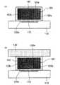
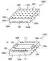
図1は第1の実施の形態に係る電子装置の一例を示す図である。図1(A)は第1の実施の形態に係る電子装置の一例の要部斜視模式図、図1(B)は図1(A)のL1−L1線の位置で切断した断面模式図、図1(C)は図1(A)のL2−L2線の位置で切断した断面模式図である。First, the first embodiment will be described.
FIG. 1 is a diagram illustrating an example of an electronic apparatus according to the first embodiment. FIG. 1A is a schematic perspective view of an essential part of an example of an electronic apparatus according to the first embodiment, and FIG. 1B is a schematic cross-sectional view taken along the line L1-L1 in FIG. FIG. 1C is a schematic cross-sectional view taken along the line L2-L2 in FIG.
図1(A)〜図1(C)に示す電子装置1は、電子部品10及び電子部品20、並びに放熱部材30を備えている。電子部品10の上に電子部品20が搭載され、その電子部品20の上に放熱部材30が搭載されている。 An electronic device 1 illustrated in FIGS. 1A to 1C includes an
電子部品10には、半導体素子、半導体素子を備える半導体装置(半導体パッケージ)、回路基板等を用いることができる。電子部品20には、半導体素子、半導体パッケージ等を用いることができる。例えば、電子部品10には、回路基板が用いられ、電子部品20には、その下面20bや側面20e及び側面20fに端子を有する半導体パッケージが用いられる。 As the
放熱部材30には、良好な熱伝導性を有する材料が用いられる。例えば、銅(Cu)、アルミニウム(Al)等の金属材料、セラミック材料、カーボン材料が放熱部材30に用いられる。放熱部材30は、例えば、プレート状とされる。放熱部材30には、針状や板状のフィンを備えたものを用いてもよい。 A material having good thermal conductivity is used for the
電子装置1は更に、図1(A)〜図1(C)に示すように、電子部品10と放熱部材30の間に配置される電子部品20の、その上面20a及び下面20b並びに対向する側面20c及び側面20dに連続して設けられた導体層40を備えている。導体層40は、電子部品20のもう一対の対向する側面20e,20fを除き、電子部品20を包囲するように設けられる。導体層40は、このように電子部品20を包囲するように設けられ、電子部品20と熱的に接続されている。 As shown in FIGS. 1 (A) to 1 (C), the electronic device 1 further has an
導体層40には、良好な熱伝導性を有する材料が用いられる。導体層40には、例えば、半田が用いられる。導体層40には、半田のほか、Cu、Al等の金属材料、セラミック材料、カーボン材料等を用いることもできる。 A material having good thermal conductivity is used for the
尚、電子部品20としてその下面20bに端子を有するものが用いられる場合、電子部品20の下面20bに設けられる導体層40の部分は、電子部品20の端子と電気的に独立して設けられる。電子部品20の下面20bに設けられる導体層40の部分は、電子部品20の処理動作を損なわなければ電子部品20の端子と電気的に接続されてもよい。 In addition, when what has a terminal in the
電子部品10及び放熱部材30は、それぞれ電子部品20の下方及び上方に、導体層40に熱的に接続されて、配置されている。例えば、半田が用いられた導体層40に、電子部品10及び放熱部材30が接合される。或いは、半田以外の材料が用いられた導体層40に、半田を用いて電子部品10及び放熱部材30が接合される。 The
上記のような構成を有する電子装置1では、電子部品10と電子部品20の少なくとも一方に、動作時に発熱するものが用いられる場合がある。例えば、半導体素子や半導体パッケージ等が用いられる電子部品20に発熱部品が採用される。電子装置1の内部の熱は、導体層40を介して熱的に接続された、電子部品10と電子部品20との間、及び電子部品20と放熱部材30との間を伝熱され、電子部品10や電子部品20から、及び放熱部材30から、電子装置1の外部へと放熱される。 In the electronic device 1 having the above-described configuration, a device that generates heat during operation may be used for at least one of the
電子装置1では、導体層40に熱伝導性の良い材料を用いることで、電子部品20の下面20bと電子部品10との間、及び電子部品20の上面20aと放熱部材30との間で、効率的な伝熱が可能になる。 In the electronic device 1, by using a material having good thermal conductivity for the
電子装置1では、電子部品20の対向する側面20c及び側面20dに、上面20a及び下面20bから連続する導体層40が設けられている。このように側面20c及び側面20dにも導体層40が設けられていることで、これが電子部品20の側面20c及び側面20dの熱伝導パスとなり、電子部品20を挟んで配置された電子部品10と放熱部材30との間における効率的な伝熱が可能になる。 In the electronic device 1, the
更に、この電子装置1では、電子部品20の側面20c及び側面20dに導体層40が設けられていることで、電子部品20の熱を、その側面20c及び側面20dの導体層40から電子装置1の外部へと効率的に放熱することができる。即ち、電子部品20の側面20c及び側面20dの導体層40は、電子部品10と放熱部材30との間の熱伝導パスとなるほか、熱を外部へ放熱する放熱部材としても機能する。 Furthermore, in this electronic device 1, since the
電子装置1では、導体層40による電子部品10、電子部品20及び放熱部材30の間での効率的な伝熱と、導体層40からの放熱により、電子部品10や電子部品20から、及び放熱部材30から、熱を電子装置1の外部へと効率的に放熱することができる。 In the electronic device 1, heat is efficiently transferred between the
このように、電子部品10と放熱部材30の間に配置される電子部品20に、その上面20a及び下面20b並びに対向する側面20c及び側面20dを包囲する導体層40を設けることで、電子装置1の放熱性を高めることが可能になる。これにより、電子部品20の過熱、電子部品10の過熱を抑制することが可能になり、電子部品20や電子部品10、更にはこれらを備える電子装置1の、熱に起因した性能劣化や故障の発生を抑制し、性能、信頼性の高い電子装置1を実現することが可能になる。 As described above, the
次に、第2の実施の形態について説明する。
図2は第2の実施の形態に係る電子装置の一例を示す図である。図2(A)は第2の実施の形態に係る電子装置の一例の断面模式図、図2(B)は第2の実施の形態に係る電子装置の一例の平面模式図、図2(C)は第2の実施の形態に係る電子装置の一例の要部平面模式図である。図2(A)は図2(B)のL3−L3断面模式図である。図2(C)は図2(B)のX部拡大図である。Next, a second embodiment will be described.
FIG. 2 is a diagram illustrating an example of an electronic apparatus according to the second embodiment. 2A is a schematic cross-sectional view of an example of an electronic device according to the second embodiment, FIG. 2B is a schematic plan view of an example of the electronic device according to the second embodiment, and FIG. ) Is a schematic plan view of an essential part of an example of an electronic apparatus according to a second embodiment. FIG. 2A is a schematic cross-sectional view taken along line L3-L3 in FIG. FIG. 2C is an enlarged view of a portion X in FIG.
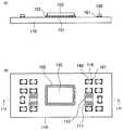
図2(A)〜図2(C)には、電子装置100として、回路基板110上に、下面に端子(後述の端子121等)を備えるレギュレータ部品120を搭載し、更にその上に放熱板130を搭載した構造を含む、FCBGA(Flip Chip Ball Grid Array)パッケージを例示している。 2A to 2C, as the
レギュレータ部品120の下面120bには、図2(C)のように、対向する側面120e及び側面120fに沿って、回路基板110の端子111に対応する位置に、複数の端子(後述の端子121)が設けられている。レギュレータ部品120は、その下面120bの端子で、回路基板110に電気的に接続されている。 On the
レギュレータ部品120には、その上面120a及び下面120b並びに対向する側面120c及び側面120dに連続して導体層140が設けられている。尚、レギュレータ部品120の下面120bの導体層140は、レギュレータ部品120の下面120bに設けられている端子(後述の端子121)とは電気的に接続されないように、設けられている。導体層140には、半田が用いられている。導体層140は、レギュレータ部品120の下方の回路基板110、及びレギュレータ部品120の上方の放熱板130に接合されている。 The
このようなレギュレータ部品120の詳細については後述する。
電子装置100は、レギュレータ部品120と共に回路基板110上に搭載された能動素子である半導体素子150、及び受動素子160を含む。Details of the
The
半導体素子150は、LSI(Large Scale Integration)等の半導体チップ、或いはそのような半導体チップを含む半導体パッケージである。半導体素子150は、半田等のバンプ151を用いて回路基板110上に実装されている。半導体素子150と回路基板110との間には、それらの接続強度を高めるため、アンダーフィル樹脂152が充填されている。半導体素子150上には、半田等の熱伝導材153を介して放熱板131が設けられている。 The
受動素子160は、コンデンサや抵抗等の部品であって、半田等の接合材161を用いて回路基板110上に実装されている。
回路基板110の表面及び内部には、端子111やそれに接続される配線及びビア等、所定の導体パターン(回路パターン)が設けられている。レギュレータ部品120、半導体素子150及び受動素子160は、それぞれ下面の端子(後述の端子121)、バンプ151及び接合材161を介して、回路基板110の所定の導体パターンに電気的に接続されている。The
Predetermined conductor patterns (circuit patterns) such as
回路基板110の、レギュレータ部品120や半導体素子150等の搭載面側と反対の面側には、回路基板110の所定の導体パターンに電気的に接続されたバンプ113が設けられている。バンプ113には、例えば半田が用いられる。 A
回路基板110上のレギュレータ部品120、半導体素子150及び受動素子160は、回路基板110上に接着剤170を用いて設けられた枠180の内側領域に搭載されている。枠180は、回路基板110の反り等の変形を抑制するスティフナとして機能する。枠180は、放熱板131と一体又は別体で形成される。放熱板130は、枠180上に、接着剤190を用いて設けられている。 The
電子装置100は、回路基板110に設けられたバンプ113を用いて、他の電子部品や電子装置に実装することができるようになっている。
ここで、上記のような電子装置100に用いられるレギュレータ部品120について更に説明する。The
Here, the
図3及び図4は第2の実施の形態に係るレギュレータ部品の一例を示す図である。図3(A)及び図3(B)は第2の実施の形態に係るレギュレータ部品の一例の外観図であって、図3(A)はレギュレータ部品を上面側から見た外観斜視模式図、図3(B)はレギュレータ部品を下面側から見た外観斜視模式図である。図4(A)及び図4(B)は第2の実施の形態に係るレギュレータ部品の断面模式図であって、図4(A)は上記図2(C)のL4−L4断面模式図、図4(B)は上記図2(C)のL5−L5断面模式図である。 3 and 4 are views showing an example of the regulator component according to the second embodiment. 3 (A) and 3 (B) are external views of an example of a regulator component according to the second embodiment, and FIG. 3 (A) is a schematic external perspective view of the regulator component viewed from the upper surface side. FIG. 3B is a schematic external perspective view of the regulator component viewed from the lower surface side. 4A and 4B are schematic cross-sectional views of the regulator component according to the second embodiment, and FIG. 4A is a schematic cross-sectional view taken along the line L4-L4 in FIG. FIG. 4B is a schematic cross-sectional view taken along line L5-L5 in FIG.
レギュレータ部品120は、回路基板110上に半導体素子150と共に搭載され、半導体素子150へ供給する電圧、電流を一定に保つ制御を行う。図3(A)及び図3(B)並びに図4(A)及び図4(B)には、レギュレータ部品120の一例として、DFN(Dual Flatpack No-leaded)パッケージを図示している。 The
レギュレータ部品120は、図3(A)及び図3(B)に示すように、その下面120bに、側面120e及び側面120fに沿って設けられた、複数の端子121を備えている。レギュレータ部品120は、この下面120bの端子121群を用いて、上記回路基板110と電気的に接続される。 As shown in FIG. 3A and FIG. 3B, the
更に、レギュレータ部品120は、図3(B)に示すように、その下面120bに、端子121群とは電気的に独立した端子122を備えている。この下面120bの端子122は、動作時に発熱するレギュレータ部品120から熱を放熱するための放熱板として機能する。尚、端子122は、レギュレータ部品120を回路基板110と電気的に接続するための電気的な端子として機能させてもよい。 Further, as shown in FIG. 3B, the
レギュレータ部品120は、図4(A)及び図4(B)に示すように、端子121、端子122、半導体素子123、ワイヤ124及び封止樹脂125を含む。半導体素子123は、放熱板として機能する端子122上に搭載される。半導体素子123は、上記回路基板110との電気接続に用いる端子121と、ワイヤ124で接続される。端子121、端子122、半導体素子123及びワイヤ124は、端子121の一部の表面及び端子122の一部の表面が露出するように、封止樹脂125で封止される。 As shown in FIGS. 4A and 4B, the
図3(A)及び図3(B)に示す外観のレギュレータ部品120は、例えばこの図4(A)及び図4(B)に示すような内部構成を有している。
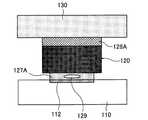
レギュレータ部品120の端子121は、それに対応する位置に設けられた回路基板110の端子111に、半田等の接合材126を用いて接合される。これにより、レギュレータ部品120と回路基板110とが電気的に接続される。The external appearance of the
The
レギュレータ部品120は、図4(A)及び図4(B)に示すように、上面120a及び下面120b並びに側面120c及び側面120dに連続して設けられた導体層140によって包囲される。導体層140には、例えば、半田が用いられる。 As shown in FIGS. 4A and 4B, the
レギュレータ部品120の下面120bの導体層140は、レギュレータ部品120の端子122(放熱板)に対応する位置に設けられた回路基板110の端子112に接合される。レギュレータ部品120は、端子122、導体層140及び端子112によって、回路基板110と熱的に接続される。尚、レギュレータ部品120は、これを回路基板110と電気的に接続する上記の端子121、接合材126及び端子111によっても、回路基板110と熱的に接続される。 The
レギュレータ部品120の上面120aの導体層140は、放熱板130に接合される。これにより、レギュレータ部品120と回路基板110とが熱的に接続される。
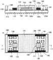
図5は第2の実施の形態に係る電子装置の組み立て工程の一例を示す図である。図5(A)は第2の実施の形態に係るレギュレータ部品配置工程の一例の要部断面模式図、図5(B)は第2の実施の形態に係る放熱板配置工程の一例の要部断面模式図である。The
FIG. 5 is a diagram illustrating an example of an assembly process of the electronic device according to the second embodiment. FIG. 5A is a schematic cross-sectional view of an essential part of an example of a regulator component arranging process according to the second embodiment, and FIG. 5B is an essential part of an example of a radiator plate arranging process according to the second embodiment. It is a cross-sectional schematic diagram.
組み立て時には、まず、図5(A)に示すように、上面120a及び下面120b並びに側面120c及び側面120dを包囲する連続した導体層140が設けられたレギュレータ部品120を、回路基板110上に配置する。次いで、図5(B)に示すように、レギュレータ部品120を包囲する導体層140上に、放熱板130を配置する。そして、導体層140を回路基板110(その端子112)及び放熱板130に接合する。例えば、半田を用いた導体層140の加熱、溶融により、導体層140を回路基板110及び放熱板130に接合する。 At the time of assembly, first, as shown in FIG. 5A, the
このような方法により、回路基板110、レギュレータ部品120及び放熱板130を、導体層140を用いて互いに接合することができる。
ところで、レギュレータ部品120は、動作時に発熱し得る。熱によってレギュレータ部品120が保証温度以上になると、その内部の配線の抵抗上昇等によって、動作速度が遅くなる場合がある。また、レギュレータ部品120が高温になる状態を含むような環境での使用が続くと、用いられている材料の劣化や昇降温の繰り返しで生じる応力負荷ダメージ等の長期的な影響によって、レギュレータ部品120の寿命が短くなる。レギュレータ部品120の過熱は、レギュレータ部品120のほか、これと接続される他の電子部品を含むデバイスの性能、信頼性を低下させる恐れがある。By such a method, the
Incidentally, the
これに対し、上記電子装置100では、レギュレータ部品120の上面120a及び下面120b並びに側面120c及び側面120dを包囲する、連続した導体層140により、レギュレータ部品120の過熱を効果的に抑制する。 On the other hand, in the
即ち、電子装置100では、導体層140が設けられていることで、レギュレータ部品120の下面120bと回路基板110との間、及びレギュレータ部品120の上面120aと放熱板130との間で、効率的な伝熱が可能になる。電子装置100では、レギュレータ部品120の側面20c及び側面20dにも導体層40が設けられていることで、これが、レギュレータ部品120を挟んで配置される回路基板110と放熱板130との間の熱伝導パスとなる。これにより、回路基板110と放熱板130との間の効率的な伝熱が可能になる。更に、この電子装置100では、レギュレータ部品120の側面120c及び側面120dの導体層40が放熱部材として機能し、レギュレータ部品120の熱を外部へと効率的に放熱することができる。 In other words, in the
このように電子装置100では、導体層140により、回路基板110、レギュレータ部品120及び放熱板130の間での効率的な伝熱と、レギュレータ部品120の側面120c及び側面120dの導体層140からの効率的な放熱が実現される。これにより、レギュレータ部品120で発生した熱を、回路基板110や放熱板130に効率的に伝熱してそれらから放熱すると共に、露出する導体層140からも効率的に放熱して、レギュレータ部品120の過熱を効果的に抑制することができる。 As described above, in the
レギュレータ部品120、更にはこれを備える電子装置100の、熱に起因した性能劣化や故障の発生を抑制し、性能、信頼性の高い電子装置100を実現することが可能になる。 It is possible to suppress the performance deterioration and failure caused by the heat of the
ここで、レギュレータ部品120に上記のような導体層140を設けない形態の電子装置の一例について述べる。
図6及び図7は別形態に係る電子装置の一例を示す図である。図6(A)は別形態に係る電子装置の一例の断面模式図、図6(B)は別形態に係る電子装置の一例の平面模式図、図6(C)は別形態に係る電子装置の一例の要部平面模式図である。図6(A)は図6(B)のL6−L6断面模式図である。図6(C)は図6(B)のY部拡大図である。また、図7(A)は図6(C)のL7−L7断面模式図、図7(B)は図6(C)のL8−L8断面模式図である。Here, an example of an electronic device in which the above-described
6 and 7 are diagrams illustrating an example of an electronic apparatus according to another embodiment. 6A is a schematic cross-sectional view of an example of an electronic device according to another embodiment, FIG. 6B is a schematic plan view of an example of an electronic device according to another embodiment, and FIG. 6C is an electronic device according to another embodiment. It is a principal part plane schematic diagram of an example. 6A is a schematic cross-sectional view taken along line L6-L6 of FIG. FIG. 6C is an enlarged view of a Y portion in FIG. 7A is a schematic cross-sectional view taken along line L7-L7 in FIG. 6C, and FIG. 7B is a schematic cross-sectional view taken along line L8-L8 in FIG.
また、図8は別形態に係る電子装置の組み立て工程の一例を示す図である。図8(A)は別形態に係るレギュレータ部品配置工程の一例の要部断面模式図、図8(B)は別形態に係る接合材配置工程の一例の要部断面模式図、図8(C)は別形態に係る放熱板配置工程の一例の要部断面模式図である。 Moreover, FIG. 8 is a figure which shows an example of the assembly process of the electronic device which concerns on another form. 8A is a schematic cross-sectional view of an essential part of an example of a regulator component placement process according to another embodiment, FIG. 8B is a schematic cross-sectional view of an essential part of an example of a bonding material placement process according to another embodiment, and FIG. ) Is a schematic cross-sectional view of an essential part of an example of a heat sink arrangement step according to another embodiment.
図6(A)〜図6(C)並びに図7(A)及び図7(B)に示す電子装置100Aは、上記のようなレギュレータ部品120を包囲する導体層140を含んでいない点で、上記第2の実施の形態に係る電子装置100と相違する。電子装置100Aでは、レギュレータ部品120(その端子122)が、接合材127Aを介して回路基板110(その端子112)に接合され、接合材128Aを介して放熱板130に接合されている。例えば、レギュレータ部品120と回路基板110とを接合する接合材127Aには半田が用いられ、レギュレータ部品120と放熱板130とを接合する接合材128Aには樹脂が用いられる。 The
組み立て時には、図8(A)に示すように、回路基板110の端子112上に半田等の接合材127Aが供給され、その上にレギュレータ部品120が配置されて、レギュレータ部品120と回路基板110とが接合材127Aで接合される。例えば、半田を用いた接合材127Aの加熱、溶融により、接合材127Aを介してレギュレータ部品120と回路基板110とが接合される。接合されたレギュレータ部品120上には、図8(B)に示すように、樹脂等の接合材128Aが供給される。そして、図8(C)に示すように、接合材128A上に放熱板130が配置され、レギュレータ部品120と放熱板130とが接合材128Aで接合される。 At the time of assembly, as shown in FIG. 8A, a
このように組み立てられる構造部を含む電子装置100A(図6及び図7)では、レギュレータ部品120と回路基板110との間の伝熱が接合材127Aを介して行われ、レギュレータ部品120と放熱板130との間の伝熱が接合材128Aを介して行われる。 In the
電子装置100Aでは、接合材128Aの熱伝導率が低いと、レギュレータ部品120から放熱板130への伝熱効率が低くなる。また、電子装置100Aでは、レギュレータ部品120の側面に封止樹脂125が露出する構造のため、レギュレータ部品120自体からの放熱性は高くない。レギュレータ部品120の熱が接合材127Aを介して回路基板110に伝熱されても、回路基板110からの放熱にも限界がある。電子装置100Aでは、例えばこのようなことが要因となって、レギュレータ部品120に過熱が生じる恐れがある。 In the
これに対し、上記第2の実施の形態に係る電子装置100(図2〜図5)は、レギュレータ部品120の上面120a及び下面120b並びに側面120c及び側面120dを包囲する連続した導体層140を含む。この導体層140により、回路基板110、レギュレータ部品120及び放熱板130の間での効率的な伝熱と、レギュレータ部品120の側面120c及び側面120dの導体層140からの効率的な放熱を可能にしている。これにより、電子装置100では、レギュレータ部品120の過熱を効果的に抑制することが可能になっている。 On the other hand, the electronic device 100 (FIGS. 2 to 5) according to the second embodiment includes the
また、図6及び図7に示したような電子装置100Aでは、次の図9に示すような不具合が生じる可能性がある。
図9は別形態に係る電子装置で生じ得る不具合の一例について説明する図である。図9(A)は別形態に係る電子装置を加熱した時の状態の一例を示す図、図9(B)は別形態に係る電子装置を加熱後に冷却した時の状態の一例を示す図である。Further, in the
FIG. 9 is a diagram for explaining an example of a problem that may occur in an electronic device according to another embodiment. 9A is a diagram illustrating an example of a state when an electronic device according to another embodiment is heated, and FIG. 9B is a diagram illustrating an example of a state when the electronic device according to another embodiment is cooled after heating. is there.
例えば、電子装置100Aは、組み立て後、回路基板110に設けられたバンプ113を用いて、他の電子装置等に実装される(二次実装)。二次実装は、半田を用いたバンプ113を、リフロー加熱によって溶融させる工程を含む。レギュレータ部品120の接合材127Aに用いられている半田の融点が、回路基板110のバンプ113に用いられている半田の融点と同等若しくは低い場合には、この二次実装時のリフロー加熱でレギュレータ部品120の接合材127Aも溶融することがある。 For example, the
二次実装時のリフロー加熱では、回路基板110にうねり等の変形が生じ得る。回路基板110にこのような変形が生じると、図9(A)に示すように、回路基板110と放熱板130との間隔が狭くなる場合がある。二次実装時のリフロー加熱により、バンプ113と共に、回路基板110とレギュレータ部品120との間の接合材127Aも溶融した状態で、このように回路基板110と放熱板130との間隔が狭くなると、溶融した接合材127Aが押し潰される。そして、接合材127Aが押し潰されると、その一部(図9(A)では接合材127Aaとして図示)が回路基板110とレギュレータ部品120との間から外に飛び出してしまうという現象が発生する。 In the reflow heating during the secondary mounting, the
図9(A)のようになった状態からリフロー加熱を終了して冷却を開始すると、回路基板110には、生じていたうねり等の変形が元に戻ろうとする力が作用する。このような力が作用することで、今度は図9(B)に示すように、回路基板110と放熱板130との間隔が広がることが起こり得る。このように回路基板110と放熱板130との間隔が広がる間に、リフロー加熱時に溶融した接合材127A、及び飛び出した接合材127Aaが、冷却により凝固する。回路基板110とレギュレータ部品120との間は、一部の接合材127Aaが飛び出してしまっているため、リフロー加熱前の当初よりも少量の接合材127Aで接合された状態になる。 When the reflow heating is finished and the cooling is started from the state as shown in FIG. 9A, a force is applied to the
回路基板110とレギュレータ部品120との間から飛び出した接合材127Aaが、回路基板110上の端子や配線等の導体パターンに飛散してしまっていると、短絡を発生させる可能性がある。また、一部の接合材127Aaが飛び出してしまったことで、回路基板110とレギュレータ部品120との間を接合する接合材127Aの量が減り、回路基板110とレギュレータ部品120との間の熱抵抗が増大し、放熱性が悪化する可能性がある。更に、回路基板110とレギュレータ部品120との間の接合材127Aが減ったことで、電子装置100Aの使用時の温度変化で接合材127Aにかかるストレスでクラックが生じ易くなり、放熱性が悪化する可能性がある。 If the bonding material 127Aa protruding from between the
これに対し、上記第2の実施の形態に係る電子装置100(図2〜図5)では、二次実装時のリフロー加熱でも、短絡や放熱性の悪化を抑制することができる。この点について、次の図10を参照して説明する。 On the other hand, in the electronic device 100 (FIGS. 2 to 5) according to the second embodiment, it is possible to suppress a short circuit and deterioration of heat dissipation even by reflow heating at the time of secondary mounting. This will be described with reference to FIG.
図10は第2の実施の形態に係る電子装置について説明する図である。図10(A)は第2の実施の形態に係る電子装置を加熱した時の状態の一例を示す図、図10(B)は第2の実施の形態に係る電子装置を加熱後に冷却した時の状態の一例を示す図である。 FIG. 10 is a diagram for explaining an electronic apparatus according to the second embodiment. FIG. 10A is a diagram illustrating an example of a state when the electronic device according to the second embodiment is heated, and FIG. 10B is a time when the electronic device according to the second embodiment is cooled after heating. It is a figure which shows an example of the state of.
導体層140に用いられている半田の融点が、回路基板110のバンプ113に用いられている半田の融点と同等若しくは低い場合には、二次実装時のリフロー加熱で導体層140が溶融し得る。 When the melting point of the solder used for the
この二次実装時のリフロー加熱の際、回路基板110にうねり等の変形が生じると、図10(A)に示すように、回路基板110と放熱板130との間隔を狭めようとする力、それにより、溶融した導体層140を押し潰そうとする力が作用する。しかし、電子装置100では、レギュレータ部品120を包囲する導体層140が全体的に溶融するため、導体層140を押し潰そうとする力が、レギュレータ部品120と回路基板110との間、及びレギュレータ部品120と放熱板130との間の、上下の部分に分散する。その結果、電子装置100では、導体層140が押し潰される量(変位量)が小さくなり、導体層140が、レギュレータ部品120の周囲から離れて外に飛び出してしまうのを抑制することができる。 When reflow heating at the time of secondary mounting causes deformation such as undulation in the
電子装置100では、レギュレータ部品120の側面120c及び側面120dにも導体層140が設けられている。そのため、回路基板110と放熱板130との間隔が狭まり、導体層140が押し潰されても、レギュレータ部品120と回路基板110又は放熱板130との間から飛び出そうとする導体層140が、図10(A)のように側面120cや側面120dに誘導される(図中点線矢印で図示)。このようにレギュレータ部品120と回路基板110又は放熱板130との間から飛び出そうとする一部の導体層140aは、レギュレータ部品120の側面120cや側面120d(ここでは側面120cの場合を例示)に誘導され、トラップされる。これにより、押し潰された導体層140が、レギュレータ部品120の周囲から離れて外に飛び出してしまうのを一層効果的に抑制することができる。 In the
図10(A)のような状態からリフロー加熱を終了して冷却を開始すると、回路基板110に生じていたうねり等の変形が元に戻ろうとし、電子装置100には、図10(B)に示すように、回路基板110と放熱板130との間隔を広げようとする力が作用する。その際は、レギュレータ部品120の側面120c及び側面120dに誘導されてトラップされていた一部の導体層140aが、表面張力により、回路基板110との間、放熱板130との間を含む、レギュレータ部品120の周囲に戻る(図中点線矢印で図示)。これにより、レギュレータ部品120と回路基板110及び放熱板130との間に、一定量の導体層140が存在する状態が得られる。 When the reflow heating is finished and the cooling is started from the state shown in FIG. 10A, the deformation such as the undulation generated in the
このように電子装置100では、溶融した導体層140の飛散を抑制することができ、導体層140の飛散による短絡を効果的に抑制することができる。更に、電子装置100では、レギュレータ部品120と回路基板110及び放熱板130との間の導体層140の不足、不足に起因した放熱性の悪化を効果的に抑制することができる。 Thus, in the
また、図6及び図7に示したような電子装置100Aでは、次の図11に示すような不具合が生じる可能性もある。
図11は別形態に係る電子装置で生じ得る不具合の別例について説明する図である。図11は別形態に係る電子装置の一例の要部断面模式図である。Further, in the
FIG. 11 is a diagram for explaining another example of a problem that may occur in an electronic device according to another embodiment. FIG. 11 is a schematic cross-sectional view of an essential part of an example of an electronic apparatus according to another embodiment.
電子装置100Aでは、レギュレータ部品120と回路基板110との間を、半田を用いた接合材127Aで接合する際(図8(A))、その接合材127Aに空気が混入し、図11に示すようなボイド129が発生することが起こり得る。その場合、このようなボイド129が含まれる接合材127Aで回路基板110に接合されたレギュレータ部品120の上に、樹脂等の接合材128Aを用いて放熱板130が接合される。ボイド129は、レギュレータ部品120と回路基板110との間の伝熱効率を低下させ、その結果、レギュレータ部品120からの放熱を妨げ、レギュレータ部品120の過熱を引き起こす一因となり得る。 In the
品質向上のため、ボイド129のサイズを規定したX線検査等の製品出荷前検査を実施し、一定サイズ以上のボイド129を含む製品をリジェクトする場合、リジェクト分は損失となってしまい、製品コストの増加の一因となりかねない。レギュレータ部品120と回路基板110との間の接合材127Aによる接合を真空加熱で行う等、ボイド129の発生を抑える技術もあるが、それを実現するための設備費用がかかるほか、製造工程の複雑化や製造コストの増加を招く可能性がある。 In order to improve quality, when pre-shipment inspection such as X-ray inspection that defines the size of the void 129 is performed and a product containing the
これに対し、上記第2の実施の形態に係る電子装置100(図2〜図5)では、導体層140にボイド129が含まれる場合でも、放熱性の悪化、コストの増加を抑制することができる。この点について、次の図12を参照して説明する。 On the other hand, in the electronic device 100 (FIGS. 2 to 5) according to the second embodiment, even when the
図12は第2の実施の形態に係る電子装置について説明する図である。図12は第2の実施の形態に係る電子装置の一例の要部断面模式図である。
電子装置100では、半田を用いた導体層140が、レギュレータ部品120の上面120a及び下面120b並びに側面120c及び側面120dを包囲するように設けられている。そのため、レギュレータ部品120と放熱板130との間の伝熱効率が比較的高く、レギュレータ部品120の熱を、効率的に放熱板130へと伝熱し、放熱板130から電子装置100の外部へと放熱することができる。更に、電子装置100では、レギュレータ部品120の熱を、その側面120c及び側面120dに設けられている導体層140から外部へと放熱することができる。FIG. 12 is a diagram for explaining an electronic apparatus according to the second embodiment. FIG. 12 is a schematic cross-sectional view of an essential part of an example of an electronic apparatus according to the second embodiment.
In the
電子装置100では、たとえ図12に示すように導体層140内にボイド129が含まれていても、レギュレータ部品120の熱を、上面120a、側面120c及び側面120dの導体層140の部分で伝熱、放熱することができる。これにより、ボイド129による伝熱効率の低下、放熱効率の低下を抑制することができる。その結果、ボイド129の発生を抑える技術を実現するための設備費用、そのような技術を採用することによる製造工程の複雑化や製造コストの増加を回避することが可能になり、電子装置100の低コスト化を図ることが可能になる。 In the
続いて、上記のような電子装置100の製造方法の一例について説明する。
図13〜図19は第2の実施の形態に係る電子装置製造方法の一例を示す図である。以下、図13〜図19を参照し、各製造工程について順に説明する。Then, an example of the manufacturing method of the above
13 to 19 are views showing an example of an electronic device manufacturing method according to the second embodiment. Hereinafter, each manufacturing process will be described in order with reference to FIGS.
導体層140を設けたレギュレータ部品120の準備工程について述べる。
図13は第2の実施の形態に係るレギュレータ部品準備工程の一例を示す図であって、図13(A)は導体シートの平面模式図、図13(B)は導体シート配置後のレギュレータ部品を上面側から見た外観斜視模式図、図13(C)は導体シート配置後のレギュレータ部品を下面側から見た外観斜視模式図である。A preparation process of the
FIG. 13 is a diagram illustrating an example of a regulator component preparation process according to the second embodiment. FIG. 13A is a schematic plan view of a conductor sheet, and FIG. 13B is a regulator component after the conductor sheet is arranged. FIG. 13C is an external perspective schematic view of the regulator component after the conductor sheet is disposed from the lower surface side.
ここでは、図13(A)に示すような導体シート141を準備する。導体シート141は、上記図3(A)及び図3(B)に示したようなレギュレータ部品120に巻き付けて上記導体層140とするものであり、例えば半田を用いて形成される。導体シート141は、それが巻き付けられるレギュレータ部品120の上面120aに対応する第1部分141a、下面120bに対応する第2部分141b、側面120cに対応する第3部分141c、側面120dに対応する第4部分141dを含む。 Here, a
このような導体シート141を、レギュレータ部品120の上面120a、側面120c、下面120b、側面120dに順に巻き付け、両端の第4部分141dと第1部分141aとを接続する。これにより、図13(B)及び図13(C)に示すように導体シート141が巻き付けられ、一続きの導体シート141即ち導体層140が設けられたレギュレータ部品120が得られる。 Such a
導体シート141の第1部分141aは、レギュレータ部品120の上面120aを覆うような平面サイズで形成される。導体シート141の第2部分141bは、レギュレータ部品120の下面120bに、側面120e及び側面120fに沿って設けられる端子121群と、接触しないような平面サイズで形成され、第1部分141aよりも幅の狭い平面サイズで形成される。導体シート141の第3部分141c及び第4部分141dはそれぞれ、第1部分141aと繋がる箇所から第2部分141bと繋がる箇所に向かって幅の狭くなる平面形状で形成される。 The
このような平面サイズ、平面形状の導体シート141を、レギュレータ部品120を包囲するように巻き付け、回路基板110との電気接続用の端子121(図3(A))を導体層140から露出させ、放熱用の端子122(図3(B))を導体層140で被覆する。これにより、図13(B)及び図13(C)に示すような導体層140が設けられたレギュレータ部品120を得る。 A
用いるレギュレータ部品120の形態に合わせた平面サイズ、平面形状の導体シート141を準備し、それを巻き付けることで、導体層140を設けたレギュレータ部品120を準備する。 A
尚、このような導体層140を設けたレギュレータ部品120は、後述するレギュレータ部品配置工程(図17)までに行われていればよい。
図14は第2の実施の形態に係る受動素子配置工程の一例を示す図であって、図14(A)は受動素子配置工程の断面模式図、図14(B)は受動素子配置工程の平面模式図である。図14(A)は図14(B)のL9−L9断面模式図である。It should be noted that the
14A and 14B are diagrams showing an example of a passive element placement process according to the second embodiment. FIG. 14A is a schematic cross-sectional view of the passive element placement process, and FIG. 14B is a passive element placement process. It is a plane schematic diagram. FIG. 14A is a schematic cross-sectional view taken along line L9-L9 in FIG.
まず、図14(A)及び図14(B)に示すような回路基板110を準備する。回路基板110には、プリント基板を用いることができる。
回路基板110は、図14(B)に示すように、レギュレータ部品120の搭載領域に設けられた端子111及び端子112、並びに、半導体素子150の搭載領域に設けられた端子115、及び受動素子160の搭載領域に設けられた端子116を備えている。これらの端子111及び端子112、並びに端子115及び端子116は、回路基板110に設けられた図示しない導体パターンに電気的に接続されている。First, a
As shown in FIG. 14B, the
準備した回路基板110の端子116上に、印刷法やディスペンス法等を用いて半田ペーストを供給し、コンデンサ等の受動素子160を配置する。そして、その半田ペーストに含まれる半田の融点以上のリフロー加熱を行う。これにより、図14(A)及び図14(B)に示すように、回路基板110(その端子116)に接合材161を介して受動素子160を接合する。 A solder paste is supplied onto the
図15は第2の実施の形態に係る半導体素子配置工程の一例を示す図であって、図15(A)は半導体素子配置工程の断面模式図、図15(B)は半導体素子配置工程の平面模式図である。図15(A)は図15(B)のL10−L10断面模式図である。 15A and 15B are diagrams illustrating an example of a semiconductor element placement process according to the second embodiment. FIG. 15A is a schematic cross-sectional view of the semiconductor element placement process, and FIG. It is a plane schematic diagram. FIG. 15A is a schematic cross-sectional view taken along line L10-L10 in FIG.
受動素子160の接合後、回路基板110の端子115上に、半田を用いたバンプ151を設けた半導体素子150を配置し、そのバンプ151に含まれる半田の融点以上のリフロー加熱を行う。これにより、図15(A)及び図15(B)に示すように、回路基板110(その端子115)にバンプ151を介して半導体素子150を接合する。 After the
尚、回路基板110の端子115上には、半導体素子150のバンプ151を接合する前に予め、半田ペーストを供給しておいてもよい。この場合は、リフロー加熱により、その半田ペース中の半田及びバンプ151を溶融、一体化し、それにより回路基板110と半導体素子150とを接合する。 Note that solder paste may be supplied in advance on the
回路基板110と半導体素子150との接合後は、図15(A)及び図15(B)に示すように、それらの間にアンダーフィル樹脂152を供給する。これにより、回路基板110と半導体素子150との間の接続強度の向上が図られる。 After the
図16は第2の実施の形態に係る第1放熱板配置工程の一例を示す図であって、図16(A)は第1放熱板配置工程の断面模式図、図16(B)は第1放熱板配置工程の平面模式図である。図16(A)は図16(B)のL11−L11断面模式図である。 FIG. 16 is a diagram illustrating an example of the first heat sink arrangement process according to the second embodiment, in which FIG. 16A is a schematic cross-sectional view of the first heat sink arrangement process, and FIG. It is a plane schematic diagram of 1 heat sink arrangement process. FIG. 16A is a schematic cross-sectional view taken along line L11-L11 in FIG.
受動素子160及び半導体素子150の接合後は、図16(A)及び図16(B)に示すように、回路基板110上に放熱板131を配置する。
放熱板131は、例えば、枠180と一体の部品として準備される。回路基板110に接合した半導体素子150の上に、半田を用いた熱伝導材153を供給し、その上に、放熱板131(及び枠180)を配置し、加熱により、熱伝導材153を介して放熱板131を半導体素子150に接合する。放熱板131と枠180とが一体の場合は、この放熱板131の接合と共に、枠180を接着剤170で回路基板110上に接着する。After the
The
尚、放熱板131と枠180とを別体の部品とする場合には、枠180を接着剤170で回路基板110上に接着した後、その枠180上に接着剤等で放熱板131を接着すると共に、その放熱板131を半導体素子150上に熱伝導材153で接合する。 When the
放熱板131には、図16(A)に示すように、半導体素子150の周りを囲むように突起131aが設けられる。突起131aを設けることで、放熱板131と半導体素子150とを接合する際、半田を用いた熱伝導材153がリフロー加熱で溶融しても、その熱伝導材153が半導体素子150の周囲の回路基板110上に流出或いは飛散して短絡を引き起こすことを抑制する。 As shown in FIG. 16A, the
放熱板131の接合後、図16(A)及び図16(B)に示すように、回路基板110の、半導体素子150等の搭載面側と反対の面側に設けられた図示しない端子上に、半田を用いたバンプ113を設ける。例えば、回路基板110の端子上に半田ボールを搭載し、リフロー加熱を行うことで、バンプ113を形成する。 After joining of the
回路基板110には、この後で行うレギュレータ部品120の配置に先立ち、例えば、図16(B)に示すように、レギュレータ部品120の搭載領域の端子111及び端子112の上に半田ペースト142が供給される。 Prior to the subsequent placement of the
図17は第2の実施の形態に係るレギュレータ部品配置工程の一例を示す図であって、図17(A)はレギュレータ部品配置工程の断面模式図、図17(B)はレギュレータ部品配置工程の平面模式図である。図17(A)は図17(B)のL12−L12断面模式図である。 FIG. 17 is a diagram illustrating an example of a regulator component placement process according to the second embodiment. FIG. 17A is a schematic cross-sectional view of the regulator component placement process, and FIG. It is a plane schematic diagram. FIG. 17A is a schematic cross-sectional view taken along line L12-L12 of FIG.
導体シート141(図13(A))を巻き付けることによって導体層140を設けたレギュレータ部品120(図13(B)及び図13(C))を、図17(A)及び図17(B)に示すように、回路基板110(その端子111及び端子112)上に配置する。 The regulator component 120 (FIGS. 13B and 13C) provided with the
導体層140を設けたレギュレータ部品120の配置に先立ち、回路基板110の端子111及び端子112の上に半田ペースト142(図16(B))を供給しておくことで、レギュレータ部品120を回路基板110上に仮固定することができる。 Prior to the arrangement of the
導体層140を設けたレギュレータ部品120の配置の際は、その導体層140から露出した電気接続用の端子121を、回路基板110の端子111上に供給した半田ペースト142の上に配置する。同時に、そのレギュレータ部品120の、放熱用の端子122を覆う導体層140を、回路基板110の端子112上に供給した半田ペースト142の上に配置する。 When the
図18は第2の実施の形態に係る接着剤配置工程の一例を示す図であって、図18(A)は接着剤配置工程の断面模式図、図18(B)は接着剤配置工程の平面模式図である。図18(A)は図18(B)のL13−L13断面模式図である。 18A and 18B are diagrams showing an example of the adhesive placement process according to the second embodiment. FIG. 18A is a schematic cross-sectional view of the adhesive placement process, and FIG. 18B is the adhesive placement process. It is a plane schematic diagram. 18A is a schematic cross-sectional view taken along line L13-L13 of FIG.
導体層140を設けたレギュレータ部品120の配置後、図18(A)及び図18(B)に示すように、枠180上に、この後に配置する放熱板130を接着するための接着剤190を配置する。 After the arrangement of the
接着剤190には、例えば、後述する導体層140の接合温度と同等若しくはそれよりも低い温度で硬化する熱硬化性樹脂、後述する導体層140の接合温度よりも高い温度で軟化する熱可塑性樹脂、紫外線照射によって硬化する紫外線硬化型樹脂等が用いられる。 Examples of the adhesive 190 include a thermosetting resin that cures at a temperature equal to or lower than the bonding temperature of the
図19は第2の実施の形態に係る第2放熱板配置工程の一例を示す図であって、図19(A)は第2放熱板配置工程の断面模式図、図19(B)は第2放熱板配置工程の平面模式図である。図19(A)は図19(B)のL14−L14断面模式図である。 FIG. 19 is a diagram illustrating an example of a second heat sink arrangement process according to the second embodiment, in which FIG. 19A is a schematic cross-sectional view of the second heat sink arrangement process, and FIG. It is a plane schematic diagram of 2 heat sink arrangement processes. FIG. 19A is a schematic cross-sectional view taken along line L14-L14 of FIG.
接着剤190を設けた枠180上に、図19(A)及び図19(B)に示すように、放熱板130を配置する。そして、導体層140及び半田ペースト142の半田が溶融する温度(接合温度)での加熱を行う。 As shown in FIGS. 19A and 19B, a
この加熱により、導体層140を、回路基板110(その端子112)に接合すると共に、枠180上に接着剤190を介して設けられた放熱板130に接合する。これにより、回路基板110、レギュレータ部品120及び放熱板130が、導体層140を介して互いに熱的に接続された状態が得られる。 By this heating, the
また、この加熱により、レギュレータ部品120の端子121(図13(A)及び図13(B))を、半田ペースト142(図4(B)に示した接合材126)を用いて、回路基板110の端子111(図16(B))に接合する。これにより、レギュレータ部品120が回路基板110に電気的に接続された状態が得られる。 Further, by this heating, the terminal 121 (FIGS. 13A and 13B) of the
例えば上記のような方法により、電子装置100を得ることができる。得られた電子装置100は、回路基板110のバンプ113を用いて、他の電子部品や電子装置に実装(二次実装)することができる。 For example, the
尚、レギュレータ部品120は、その種類によっては、高温に曝されることで性能、信頼性が低下してしまう場合がある。そのため、レギュレータ部品120に対し、例えば半田の溶融を伴うような比較的高い温度の加熱に曝すことのできる回数が制限される場合がある。上記の方法では、レギュレータ部品120に対してそのような加熱が行われるのを、図19のように導体層140を回路基板110及び放熱板130と接合する際の1回のみとすることができる。電子装置100を二次実装する際の加熱を加えても、加熱回数を2回に抑えることができる。そのため、性能、信頼性の高いレギュレータ部品120を備えた電子装置100を実現することができる。 Depending on the type of the
また、上記の電子装置100の製造方法では、レギュレータ部品120を包囲するように設けた導体層140を所定の接合温度で溶融することで、レギュレータ部品120を回路基板110と放熱板130の双方に一括で接合することができる。 In the method for manufacturing the
これに対し、上記図6及び図7に示したような電子装置100Aでは、上記図8(A)〜図8(C)に示した手順を経る。即ち、まず、回路基板110上に、例えば半田を用いた接合材127Aを供給して、その上にレギュレータ部品120を配置し、加熱により、レギュレータ部品120と回路基板110とを接合材127Aで接合する(図8(A))。次いで、接合されたレギュレータ部品120上に、例えば樹脂の接合材128Aを供給し(図8(B))、その上に放熱板130を配置し、加熱により、レギュレータ部品120と放熱板130とを接合材128Aで接合する(図8(C))。 On the other hand, in the
上記の電子装置100の製造方法では、上記図8(A)のように加熱によりレギュレータ部品120を接合材127Aで回路基板110上に接合する工程、及び、上記図8(B)のようにレギュレータ部品120上に接合材128Aを供給する工程が削減可能となる。上記のような導体層140を用いた電子装置100の製造方法によれば、その製造工数を削減することができ、製造の効率化、低コスト化を図ることが可能になる。 In the manufacturing method of the
尚、レギュレータ部品120を包囲するように設ける導体層140と、回路基板110及び放熱板130とを接合する工程(図19)では、溶融された導体層140が押し潰されるような力が作用することも起こり得る。このような場合でも、上記図10で述べたのと同様に、押し潰される導体層140の飛散は抑制され、飛散による短絡や放熱性の悪化を抑制することができる。また、上記図12のように導体層140内にボイド129が生じた場合でも、レギュレータ部品120を包囲する導体層140により、レギュレータ部品120からの放熱性の悪化を抑制することができる。 In the step of joining the
電子装置100の二次実装時には、上記図10で述べたように、導体層140の飛散、それによる短絡や放熱性の悪化が効果的に抑制される。
上記のような導体層140を用いた電子装置100の製造方法によれば、性能、信頼性の高い電子装置100を効率的に製造することができる。At the time of secondary mounting of the
According to the method for manufacturing the
次に、第3の実施の形態について説明する。
図20は第3の実施の形態に係るレギュレータ部品の一例を示す図である。図20(A)及び図20(B)は第3の実施の形態に係るレギュレータ部品の一例の外観図であって、図20(A)はレギュレータ部品を上面側から見た外観斜視模式図、図20(B)はレギュレータ部品を下面側から見た外観斜視模式図である。Next, a third embodiment will be described.
FIG. 20 is a diagram illustrating an example of a regulator component according to the third embodiment. 20A and 20B are external views of an example of a regulator component according to the third embodiment, and FIG. 20A is a schematic external perspective view of the regulator component as viewed from the upper surface side. FIG. 20B is a schematic external perspective view of the regulator component viewed from the lower surface side.
図20(A)及び図20(B)に示すレギュレータ部品120Aは、端子121及び端子122の表面が露出するように設けられた封止樹脂125の表面に、溶融した半田が濡れる材料を用いて形成された膜210(下地層)を有している。第3の実施の形態に係るレギュレータ部品120Aは、このような点で、上記第2の実施の形態に係るレギュレータ部品120と相違する。 A
膜210は、導体層140を設ける面、即ち、上面120a及び下面120b並びに側面120c及び側面120dの封止樹脂125上に、設けられる。膜210には、導体層140に用いられる半田が溶融した時に濡れる各種材料、例えばCu、ニッケル(Ni)、金(Au)等の材料を用いることができる。この図20(A)及び図20(B)のように封止樹脂125の表面に設けられた膜210上に、上記図13(A)に示したような、半田を用いた導体シート141を巻き付け、導体層140を形成する。 The
導体層140と回路基板110及び放熱板130とを接合する工程(図19)等、導体層140の半田が溶融するような温度で加熱が行われた時には、その溶融した導体層140が、下地となる膜210上に濡れ、効果的にレギュレータ部品120を包囲する。更に、溶融した導体層140の、下地となる膜210上からの流出が抑制され、溶融によって流動する半田と、下面120bの端子121との接触が効果的に抑制される。 When heating is performed at a temperature at which the solder of the
次に、第4の実施の形態について説明する。
図21は第4の実施の形態に係るレギュレータ部品の一例を示す図である。図21(A)及び図21(B)は第4の実施の形態に係るレギュレータ部品の一例の外観図であって、図21(A)はレギュレータ部品を上面側から見た外観斜視模式図、図21(B)はレギュレータ部品を下面側から見た外観斜視模式図である。図21(C)及び図21(D)は第4の実施の形態に係るレギュレータ部品の一例の断面模式図であって、図21(C)は図21(A)のL15−L15線の位置で切断した断面模式図、図21(D)は図21(A)のL16−L16線の位置で切断した断面模式図である。Next, a fourth embodiment will be described.
FIG. 21 is a diagram illustrating an example of a regulator component according to the fourth embodiment. FIGS. 21A and 21B are external views of an example of a regulator component according to the fourth embodiment, and FIG. 21A is a schematic external perspective view of the regulator component viewed from the upper surface side. FIG. 21B is a schematic external perspective view of the regulator component viewed from the lower surface side. FIG. 21C and FIG. 21D are schematic cross-sectional views of examples of regulator components according to the fourth embodiment, and FIG. 21C is the position of the line L15-L15 in FIG. FIG. 21D is a schematic cross-sectional view taken along the line L16-L16 in FIG. 21A.
図21(A)〜図21(D)に示すレギュレータ部品120Bは、封止樹脂125内の半導体素子123が搭載される放熱用の端子122が、下面120bから、対向する側面120c及び側面120dに延び、更に上面120aまで延びるように設けられている。第4の実施の形態に係るレギュレータ部品120Bは、このような点で、上記第2の実施の形態に係るレギュレータ部品120と相違する。 In the
このような形状の端子122と電気接続用の端子121との表面が露出するように、端子122、端子121、半導体素子123及びワイヤ124が封止樹脂125で封止され、図21(A)〜図21(D)に示すようなレギュレータ部品120Bが得られる。このレギュレータ部品120Bの、露出する端子122の表面に、上記図13(A)に示したような、半田を用いた導体シート141が巻き付けられ、導体層140が形成される。端子122には、熱伝導性が良く、溶融半田が濡れる材料、例えばCu、Ni、Au等の材料を用いることができる。 The terminal 122, the terminal 121, the
このレギュレータ部品120Bによれば、比較的熱伝導率の低い封止樹脂125の、パッケージ全体に占める体積を減らすと共に、半導体素子123を包囲するように設けた端子122によって放熱性を高めることができる。端子122に、溶融半田が濡れる材料を用いることで、これが下地(層)となり、上記第3の実施の形態と同様、溶融した導体層140が効果的にレギュレータ部品120を包囲し、溶融した導体層140と電気接続用の端子121との接触が効果的に抑制される。 According to the
次に、第5の実施の形態について説明する。
図22は第5の実施の形態に係るレギュレータ部品の一例を示す図である。図22(A)及び図22(B)は第5の実施の形態に係るレギュレータ部品の一例の外観図であって、図22(A)はレギュレータ部品を上面側から見た外観斜視模式図、図22(B)はレギュレータ部品を下面側から見た外観斜視模式図である。Next, a fifth embodiment will be described.
FIG. 22 is a diagram illustrating an example of a regulator component according to the fifth embodiment. 22A and 22B are external views of an example of a regulator component according to the fifth embodiment, and FIG. 22A is a schematic external perspective view of the regulator component viewed from the upper surface side. FIG. 22B is a schematic external perspective view of the regulator component viewed from the lower surface side.
図22(A)及び図22(B)に示すレギュレータ部品120Cは、端子121及び端子122の表面が露出するように設けられた封止樹脂125の表面に、複数の凹部又は凸部220を有している。第5の実施の形態に係るレギュレータ部品120Cは、このような点で、上記第2の実施の形態に係るレギュレータ部品120と相違する。 The
この図22(A)及び図22(B)のように凹部又は凸部220を設けた封止樹脂125の表面に、上記図13(A)に示したような、半田を用いた導体シート141を巻き付け、導体層140を形成する。凹部又は凸部220を設けた封止樹脂125の表面には、上記第3の実施の形態で述べたような、溶融半田が濡れる膜(図20の膜210)を設けてもよい。このように封止樹脂125の表面に凹部又は凸部220を設けることで、封止樹脂125の表面積が増大し、アンカー効果によって、導体層140とレギュレータ部品120Cとの接合強度が高められる。 A
次に、第6の実施の形態について説明する。
図23は第6の実施の形態に係る放熱板の一例を示す図である。図23(A)は第6の実施の形態に係る放熱板の第1変形例の要部断面模式図、図23(B)は第6の実施の形態に係る放熱板の第2変形例の要部断面模式図、図23(C)は第6の実施の形態に係る放熱板の第3変形例の要部断面模式図である。Next, a sixth embodiment will be described.
FIG. 23 is a diagram illustrating an example of a heat dissipation plate according to the sixth embodiment. FIG. 23A is a schematic cross-sectional view of a main part of a first modification of the heat dissipation plate according to the sixth embodiment, and FIG. 23B is a second modification of the heat dissipation plate according to the sixth embodiment. FIG. 23C is a schematic cross-sectional view of a relevant part of a third modification of the heat sink according to the sixth embodiment.
放熱板130には、レギュレータ部品120等を包囲するように設けられる導体層140との接合領域に、図23(A)に示すように、導体層140に用いられる半田が溶融した時に濡れる材料を用いた膜230を設けることができる。このような膜230には、例えばCu、Ni、Au等の材料を用いることができる。膜230は、めっき法を用いて、放熱板130の、導体層140との接合領域に、設けることができる。膜230を設けることで、放熱板130と導体層140との接合強度の向上が図られる。 As shown in FIG. 23 (A), a material that gets wet when the solder used for the
また、放熱板130には、レギュレータ部品120等を包囲するように設けられる導体層140との接合領域に、図23(B)に示すような凹部240、或いは、図23(C)に示すような凸部250を設けることもできる。このような凹部240や凸部250は、放熱板130のプレス加工、ブラスト加工等で形成することができる。また、このような凹部240や凸部250を有する部材を別途準備し、その部材を、放熱板130の、導体層140との接合領域に、設けることもできる。凹部240や凸部250の表面に、溶融半田が濡れる膜を設けてもよい。凹部240や凸部250を設けることで、導体層140との接触面積の増大によるアンカー効果により、放熱板130と導体層140との接合強度の向上が図られる。 In addition, the
1,100,100A 電子装置
10,20 電子部品
20a,120a 上面
20b,120b 下面
20c,20d,20e,20f,120c,120d,120e,120f 側面
30 放熱部材
40,140,140a 導体層
110 回路基板
111,112,115,116,121,122 端子
113,151 バンプ
120,120A,120B,120C レギュレータ部品
123,150 半導体素子
124 ワイヤ
125 封止樹脂
126,127A,127Aa,128A,161 接合材
129 ボイド
130,131 放熱板
131a 突起
141 導体シート
141a,141b,141c,141d 部分
142 半田ペースト
152 アンダーフィル樹脂
153 熱伝導材
160 受動素子
170,190 接着剤
180 枠
210,230 膜
220 凹部又は凸部
240 凹部
250 凸部1,100,100A
Claims (7)
Translated fromJapanese前記第1電子部品の上方に設けられた第2電子部品と、
前記第2電子部品の上方に設けられた放熱部材と、
前記第2電子部品の上面及び下面並びに対向する第1側面及び第2側面に連続して設けられ、前記第1電子部品及び前記放熱部材に接続された導体層と
を含むことを特徴とする電子装置。A first electronic component;
A second electronic component provided above the first electronic component;
A heat dissipating member provided above the second electronic component;
An electronic device comprising: a conductor layer provided continuously from the upper surface and the lower surface of the second electronic component and the first and second side surfaces facing each other; and a conductor layer connected to the first electronic component and the heat dissipation member. apparatus.
前記第2電子部品の上方に放熱部材を配置する工程と、
前記導体層を前記第1電子部品及び前記放熱部材と接続する工程と
を含むことを特徴とする電子装置の製造方法。A step of disposing a second electronic component having a conductor layer continuously provided on the upper surface and the lower surface and the opposing first and second side surfaces above the first electronic component;
Disposing a heat dissipating member above the second electronic component;
A step of connecting the conductor layer to the first electronic component and the heat dissipating member.
前記第2電子部品の前記上面、前記第1側面、前記下面及び前記第2側面に対応する一続きの導体シートを準備する工程と、
前記導体シートを、前記上面、前記第1側面、前記下面及び前記第2側面に貼付することによって前記導体層を形成する工程と
を含むことを特徴とする請求項5に記載の電子装置の製造方法。Before the step of arranging the second electronic component above the first electronic component,
Preparing a series of conductor sheets corresponding to the upper surface, the first side surface, the lower surface and the second side surface of the second electronic component;
The manufacturing method of an electronic device according to claim 5, further comprising: forming the conductor layer by attaching the conductor sheet to the upper surface, the first side surface, the lower surface, and the second side surface. Method.
加熱によって溶融させた前記導体層を前記第1電子部品及び前記放熱部材の双方に接合する工程を含むことを特徴とする請求項5又は6に記載の電子装置の製造方法。Connecting the conductor layer to the first electronic component and the heat dissipation member,
The method for manufacturing an electronic device according to claim 5, further comprising a step of joining the conductor layer melted by heating to both the first electronic component and the heat dissipation member.
Priority Applications (1)
| Application Number | Priority Date | Filing Date | Title |
|---|---|---|---|
| JP2015001406AJP6528406B2 (en) | 2015-01-07 | 2015-01-07 | Electronic device and method of manufacturing electronic device |
Applications Claiming Priority (1)
| Application Number | Priority Date | Filing Date | Title |
|---|---|---|---|
| JP2015001406AJP6528406B2 (en) | 2015-01-07 | 2015-01-07 | Electronic device and method of manufacturing electronic device |
Publications (2)
| Publication Number | Publication Date |
|---|---|
| JP2016127196Atrue JP2016127196A (en) | 2016-07-11 |
| JP6528406B2 JP6528406B2 (en) | 2019-06-12 |
Family
ID=56359744
Family Applications (1)
| Application Number | Title | Priority Date | Filing Date |
|---|---|---|---|
| JP2015001406AActiveJP6528406B2 (en) | 2015-01-07 | 2015-01-07 | Electronic device and method of manufacturing electronic device |
Country Status (1)
| Country | Link |
|---|---|
| JP (1) | JP6528406B2 (en) |
Cited By (1)
| Publication number | Priority date | Publication date | Assignee | Title |
|---|---|---|---|---|
| WO2022145202A1 (en)* | 2021-01-04 | 2022-07-07 | 株式会社村田製作所 | Electronic device |
Citations (11)
| Publication number | Priority date | Publication date | Assignee | Title |
|---|---|---|---|---|
| JPH05206319A (en)* | 1992-01-28 | 1993-08-13 | Mitsubishi Electric Corp | Semiconductor device and its manufacture |
| JP2001044341A (en)* | 1999-07-26 | 2001-02-16 | Tdk Corp | High-frequency module |
| JP2001274294A (en)* | 2000-03-24 | 2001-10-05 | Matsushita Electric Ind Co Ltd | Semiconductor package and method of manufacturing semiconductor package |
| US7033861B1 (en)* | 2005-05-18 | 2006-04-25 | Staktek Group L.P. | Stacked module systems and method |
| JP2007150044A (en)* | 2005-11-29 | 2007-06-14 | Denso Corp | Semiconductor device |
| JP2008218669A (en)* | 2007-03-02 | 2008-09-18 | Nec Electronics Corp | Semiconductor device |
| JP2012160634A (en)* | 2011-02-02 | 2012-08-23 | Nec Corp | Module component and manufacturing method of the same |
| US20120228751A1 (en)* | 2011-03-07 | 2012-09-13 | Samsung Electronics Co., Ltd. | Semiconductor package and method of manufacturing the same |
| JP2012253190A (en)* | 2011-06-02 | 2012-12-20 | Powertech Technology Inc | Semiconductor package and assembling method of the same |
| JP2013105884A (en)* | 2011-11-14 | 2013-05-30 | Denso Corp | Semiconductor module |
| JP2014203998A (en)* | 2013-04-05 | 2014-10-27 | 日立オートモティブシステムズ株式会社 | In-vehicle electronic controller |
- 2015
- 2015-01-07JPJP2015001406Apatent/JP6528406B2/enactiveActive
Patent Citations (11)
| Publication number | Priority date | Publication date | Assignee | Title |
|---|---|---|---|---|
| JPH05206319A (en)* | 1992-01-28 | 1993-08-13 | Mitsubishi Electric Corp | Semiconductor device and its manufacture |
| JP2001044341A (en)* | 1999-07-26 | 2001-02-16 | Tdk Corp | High-frequency module |
| JP2001274294A (en)* | 2000-03-24 | 2001-10-05 | Matsushita Electric Ind Co Ltd | Semiconductor package and method of manufacturing semiconductor package |
| US7033861B1 (en)* | 2005-05-18 | 2006-04-25 | Staktek Group L.P. | Stacked module systems and method |
| JP2007150044A (en)* | 2005-11-29 | 2007-06-14 | Denso Corp | Semiconductor device |
| JP2008218669A (en)* | 2007-03-02 | 2008-09-18 | Nec Electronics Corp | Semiconductor device |
| JP2012160634A (en)* | 2011-02-02 | 2012-08-23 | Nec Corp | Module component and manufacturing method of the same |
| US20120228751A1 (en)* | 2011-03-07 | 2012-09-13 | Samsung Electronics Co., Ltd. | Semiconductor package and method of manufacturing the same |
| JP2012253190A (en)* | 2011-06-02 | 2012-12-20 | Powertech Technology Inc | Semiconductor package and assembling method of the same |
| JP2013105884A (en)* | 2011-11-14 | 2013-05-30 | Denso Corp | Semiconductor module |
| JP2014203998A (en)* | 2013-04-05 | 2014-10-27 | 日立オートモティブシステムズ株式会社 | In-vehicle electronic controller |
Cited By (1)
| Publication number | Priority date | Publication date | Assignee | Title |
|---|---|---|---|---|
| WO2022145202A1 (en)* | 2021-01-04 | 2022-07-07 | 株式会社村田製作所 | Electronic device |
Also Published As
| Publication number | Publication date |
|---|---|
| JP6528406B2 (en) | 2019-06-12 |
Similar Documents
| Publication | Publication Date | Title |
|---|---|---|
| JP6021504B2 (en) | Printed wiring board, printed circuit board, and printed circuit board manufacturing method | |
| JP4910439B2 (en) | Semiconductor device | |
| JP4691455B2 (en) | Semiconductor device | |
| JP6569375B2 (en) | Semiconductor device, semiconductor device manufacturing method, and electronic device | |
| US9698132B1 (en) | Chip package stack up for heat dissipation | |
| JP2003318361A (en) | Semiconductor device and method of manufacturing the same | |
| US9035472B2 (en) | Semiconductor device | |
| US9721866B2 (en) | Semiconductor device having multiple bonded heat sinks | |
| JP2012191002A (en) | Semiconductor device | |
| JP2017201645A (en) | Circuit board and semiconductor integrated circuit mounting structure | |
| JP3228339B2 (en) | Semiconductor device and method of manufacturing the same | |
| JP2008016653A (en) | Semiconductor package, manufacturing method thereof, printed circuit board, and electronic device | |
| JP2014154688A (en) | Semiconductor device and manufacturing method of the same | |
| JP2007184351A (en) | Semiconductor device and its manufacturing method | |
| JP2009135391A (en) | Electronic device and method of manufacturing the same | |
| JP5799565B2 (en) | Semiconductor device and manufacturing method thereof | |
| US9018761B2 (en) | Semiconductor device | |
| JP6477105B2 (en) | Semiconductor device | |
| JP6528406B2 (en) | Electronic device and method of manufacturing electronic device | |
| JP7526642B2 (en) | Semiconductor device and its manufacturing method | |
| JP6985599B2 (en) | Electronic device and manufacturing method of electronic device | |
| US20160254241A1 (en) | Printed circuit board and soldering method | |
| KR20130092807A (en) | Thermally Enhanced Chip-On Film Package | |
| WO2017203859A1 (en) | Electronic circuit device and method | |
| JP2014022577A (en) | Semiconductor device and method of manufacturing semiconductor device |
Legal Events
| Date | Code | Title | Description |
|---|---|---|---|
| A621 | Written request for application examination | Free format text:JAPANESE INTERMEDIATE CODE: A621 Effective date:20171110 | |
| A977 | Report on retrieval | Free format text:JAPANESE INTERMEDIATE CODE: A971007 Effective date:20180717 | |
| A131 | Notification of reasons for refusal | Free format text:JAPANESE INTERMEDIATE CODE: A131 Effective date:20180724 | |
| A521 | Request for written amendment filed | Free format text:JAPANESE INTERMEDIATE CODE: A523 Effective date:20180829 | |
| A131 | Notification of reasons for refusal | Free format text:JAPANESE INTERMEDIATE CODE: A131 Effective date:20190129 | |
| A521 | Request for written amendment filed | Free format text:JAPANESE INTERMEDIATE CODE: A523 Effective date:20190320 | |
| TRDD | Decision of grant or rejection written | ||
| A01 | Written decision to grant a patent or to grant a registration (utility model) | Free format text:JAPANESE INTERMEDIATE CODE: A01 Effective date:20190416 | |
| A61 | First payment of annual fees (during grant procedure) | Free format text:JAPANESE INTERMEDIATE CODE: A61 Effective date:20190429 | |
| R150 | Certificate of patent or registration of utility model | Ref document number:6528406 Country of ref document:JP Free format text:JAPANESE INTERMEDIATE CODE: R150 |