JP2016127190A - Display device - Google Patents
Display deviceDownload PDFInfo
- Publication number
- JP2016127190A JP2016127190AJP2015001177AJP2015001177AJP2016127190AJP 2016127190 AJP2016127190 AJP 2016127190AJP 2015001177 AJP2015001177 AJP 2015001177AJP 2015001177 AJP2015001177 AJP 2015001177AJP 2016127190 AJP2016127190 AJP 2016127190A
- Authority
- JP
- Japan
- Prior art keywords
- display device
- electrode
- layer
- oxide semiconductor
- transparent conductive
- Prior art date
- Legal status (The legal status is an assumption and is not a legal conclusion. Google has not performed a legal analysis and makes no representation as to the accuracy of the status listed.)
- Pending
Links
Images


Classifications
- G—PHYSICS
- G02—OPTICS
- G02F—OPTICAL DEVICES OR ARRANGEMENTS FOR THE CONTROL OF LIGHT BY MODIFICATION OF THE OPTICAL PROPERTIES OF THE MEDIA OF THE ELEMENTS INVOLVED THEREIN; NON-LINEAR OPTICS; FREQUENCY-CHANGING OF LIGHT; OPTICAL LOGIC ELEMENTS; OPTICAL ANALOGUE/DIGITAL CONVERTERS
- G02F1/00—Devices or arrangements for the control of the intensity, colour, phase, polarisation or direction of light arriving from an independent light source, e.g. switching, gating or modulating; Non-linear optics
- G02F1/01—Devices or arrangements for the control of the intensity, colour, phase, polarisation or direction of light arriving from an independent light source, e.g. switching, gating or modulating; Non-linear optics for the control of the intensity, phase, polarisation or colour
- G02F1/13—Devices or arrangements for the control of the intensity, colour, phase, polarisation or direction of light arriving from an independent light source, e.g. switching, gating or modulating; Non-linear optics for the control of the intensity, phase, polarisation or colour based on liquid crystals, e.g. single liquid crystal display cells
- G02F1/133—Constructional arrangements; Operation of liquid crystal cells; Circuit arrangements
- G02F1/136—Liquid crystal cells structurally associated with a semi-conducting layer or substrate, e.g. cells forming part of an integrated circuit
- G02F1/1362—Active matrix addressed cells
- G02F1/136286—Wiring, e.g. gate line, drain line
- H—ELECTRICITY
- H10—SEMICONDUCTOR DEVICES; ELECTRIC SOLID-STATE DEVICES NOT OTHERWISE PROVIDED FOR
- H10D—INORGANIC ELECTRIC SEMICONDUCTOR DEVICES
- H10D30/00—Field-effect transistors [FET]
- H10D30/60—Insulated-gate field-effect transistors [IGFET]
- H10D30/67—Thin-film transistors [TFT]
- H10D30/6728—Vertical TFTs
- H—ELECTRICITY
- H10—SEMICONDUCTOR DEVICES; ELECTRIC SOLID-STATE DEVICES NOT OTHERWISE PROVIDED FOR
- H10D—INORGANIC ELECTRIC SEMICONDUCTOR DEVICES
- H10D30/00—Field-effect transistors [FET]
- H10D30/60—Insulated-gate field-effect transistors [IGFET]
- H10D30/67—Thin-film transistors [TFT]
- H10D30/6729—Thin-film transistors [TFT] characterised by the electrodes
- H10D30/673—Thin-film transistors [TFT] characterised by the electrodes characterised by the shapes, relative sizes or dispositions of the gate electrodes
- H10D30/6733—Multi-gate TFTs
- H10D30/6734—Multi-gate TFTs having gate electrodes arranged on both top and bottom sides of the channel, e.g. dual-gate TFTs
- H—ELECTRICITY
- H10—SEMICONDUCTOR DEVICES; ELECTRIC SOLID-STATE DEVICES NOT OTHERWISE PROVIDED FOR
- H10D—INORGANIC ELECTRIC SEMICONDUCTOR DEVICES
- H10D30/00—Field-effect transistors [FET]
- H10D30/60—Insulated-gate field-effect transistors [IGFET]
- H10D30/67—Thin-film transistors [TFT]
- H10D30/6729—Thin-film transistors [TFT] characterised by the electrodes
- H10D30/673—Thin-film transistors [TFT] characterised by the electrodes characterised by the shapes, relative sizes or dispositions of the gate electrodes
- H10D30/6735—Thin-film transistors [TFT] characterised by the electrodes characterised by the shapes, relative sizes or dispositions of the gate electrodes having gates fully surrounding the channels, e.g. gate-all-around
- H—ELECTRICITY
- H10—SEMICONDUCTOR DEVICES; ELECTRIC SOLID-STATE DEVICES NOT OTHERWISE PROVIDED FOR
- H10D—INORGANIC ELECTRIC SEMICONDUCTOR DEVICES
- H10D30/00—Field-effect transistors [FET]
- H10D30/60—Insulated-gate field-effect transistors [IGFET]
- H10D30/67—Thin-film transistors [TFT]
- H10D30/674—Thin-film transistors [TFT] characterised by the active materials
- H10D30/6755—Oxide semiconductors, e.g. zinc oxide, copper aluminium oxide or cadmium stannate
- H—ELECTRICITY
- H10—SEMICONDUCTOR DEVICES; ELECTRIC SOLID-STATE DEVICES NOT OTHERWISE PROVIDED FOR
- H10D—INORGANIC ELECTRIC SEMICONDUCTOR DEVICES
- H10D30/00—Field-effect transistors [FET]
- H10D30/60—Insulated-gate field-effect transistors [IGFET]
- H10D30/67—Thin-film transistors [TFT]
- H10D30/6757—Thin-film transistors [TFT] characterised by the structure of the channel, e.g. transverse or longitudinal shape or doping profile
- H—ELECTRICITY
- H10—SEMICONDUCTOR DEVICES; ELECTRIC SOLID-STATE DEVICES NOT OTHERWISE PROVIDED FOR
- H10D—INORGANIC ELECTRIC SEMICONDUCTOR DEVICES
- H10D64/00—Electrodes of devices having potential barriers
- H10D64/60—Electrodes characterised by their materials
- H10D64/62—Electrodes ohmically coupled to a semiconductor
- H—ELECTRICITY
- H10—SEMICONDUCTOR DEVICES; ELECTRIC SOLID-STATE DEVICES NOT OTHERWISE PROVIDED FOR
- H10D—INORGANIC ELECTRIC SEMICONDUCTOR DEVICES
- H10D86/00—Integrated devices formed in or on insulating or conducting substrates, e.g. formed in silicon-on-insulator [SOI] substrates or on stainless steel or glass substrates
- H10D86/40—Integrated devices formed in or on insulating or conducting substrates, e.g. formed in silicon-on-insulator [SOI] substrates or on stainless steel or glass substrates characterised by multiple TFTs
- H10D86/421—Integrated devices formed in or on insulating or conducting substrates, e.g. formed in silicon-on-insulator [SOI] substrates or on stainless steel or glass substrates characterised by multiple TFTs having a particular composition, shape or crystalline structure of the active layer
- H—ELECTRICITY
- H10—SEMICONDUCTOR DEVICES; ELECTRIC SOLID-STATE DEVICES NOT OTHERWISE PROVIDED FOR
- H10D—INORGANIC ELECTRIC SEMICONDUCTOR DEVICES
- H10D86/00—Integrated devices formed in or on insulating or conducting substrates, e.g. formed in silicon-on-insulator [SOI] substrates or on stainless steel or glass substrates
- H10D86/40—Integrated devices formed in or on insulating or conducting substrates, e.g. formed in silicon-on-insulator [SOI] substrates or on stainless steel or glass substrates characterised by multiple TFTs
- H10D86/441—Interconnections, e.g. scanning lines
- H10D86/443—Interconnections, e.g. scanning lines adapted for preventing breakage, peeling or short circuiting
- H—ELECTRICITY
- H10—SEMICONDUCTOR DEVICES; ELECTRIC SOLID-STATE DEVICES NOT OTHERWISE PROVIDED FOR
- H10D—INORGANIC ELECTRIC SEMICONDUCTOR DEVICES
- H10D86/00—Integrated devices formed in or on insulating or conducting substrates, e.g. formed in silicon-on-insulator [SOI] substrates or on stainless steel or glass substrates
- H10D86/40—Integrated devices formed in or on insulating or conducting substrates, e.g. formed in silicon-on-insulator [SOI] substrates or on stainless steel or glass substrates characterised by multiple TFTs
- H10D86/60—Integrated devices formed in or on insulating or conducting substrates, e.g. formed in silicon-on-insulator [SOI] substrates or on stainless steel or glass substrates characterised by multiple TFTs wherein the TFTs are in active matrices
- H—ELECTRICITY
- H10—SEMICONDUCTOR DEVICES; ELECTRIC SOLID-STATE DEVICES NOT OTHERWISE PROVIDED FOR
- H10D—INORGANIC ELECTRIC SEMICONDUCTOR DEVICES
- H10D99/00—Subject matter not provided for in other groups of this subclass
Landscapes
- Physics & Mathematics (AREA)
- Nonlinear Science (AREA)
- Mathematical Physics (AREA)
- Engineering & Computer Science (AREA)
- Chemical & Material Sciences (AREA)
- Crystallography & Structural Chemistry (AREA)
- Microelectronics & Electronic Packaging (AREA)
- General Physics & Mathematics (AREA)
- Optics & Photonics (AREA)
- Liquid Crystal (AREA)
- Thin Film Transistor (AREA)
- Electroluminescent Light Sources (AREA)
- Devices For Indicating Variable Information By Combining Individual Elements (AREA)
Abstract
Description
Translated fromJapanese本発明は、表示装置に関し、開示される一実施形態は表示装置に配置されたトランジスタ及び画素の構造及びレイアウト形状に関する。 The present invention relates to a display device, and one disclosed embodiment relates to the structure and layout shape of transistors and pixels arranged in the display device.
近年、表示装置やパーソナルコンピュータなどの駆動回路には微細なスイッチング素子としてトランジスタ、ダイオードなどの半導体装置が用いられている。特に、表示装置に用いられるトランジスタは、表示する映像に基づく各画素の階調に応じた電圧又は電流(データ信号)を供給するための選択トランジスタだけでなく、データ信号を供給する画素を選択するための駆動回路にも使用されている。ここで、表示装置に用いられるトランジスタはその用途に応じて要求される特性が異なる。例えば、選択トランジスタとして使用されるトランジスタは、オフ電流が低いことや複数のトランジスタ間の特性ばらつきが小さいことが要求される。また、駆動回路として使用されるトランジスタは、高いオン電流が要求される。 In recent years, semiconductor devices such as transistors and diodes are used as fine switching elements in drive circuits such as display devices and personal computers. In particular, a transistor used in a display device selects not only a selection transistor for supplying a voltage or a current (data signal) corresponding to the gradation of each pixel based on an image to be displayed but also a pixel that supplies a data signal. It is also used in the drive circuit for this purpose. Here, the transistor used for the display device has different characteristics depending on the application. For example, a transistor used as a selection transistor is required to have a low off-state current and a small variation in characteristics between a plurality of transistors. In addition, a transistor used as a driver circuit is required to have a high on-state current.
上記のような表示装置において、従来からアモルファスシリコンや低温ポリシリコン、単結晶シリコンをチャネルに用いたトランジスタによって構成された表示装置が開発されている。アモルファスシリコンや低温ポリシリコンを用いた表示装置は、600℃以下の低温プロセスで形成することができるため、ガラス基板を用いて形成することができる。特に、アモルファスシリコンを用いる場合は、より単純な構造かつ400℃以下の低温プロセスでトランジスタを形成することができるため、例えば第8世代(2160×2460mm)と呼ばれる大型のガラス基板を用いて表示装置を形成することができる。しかし、アモルファスシリコンをチャネルに用いたトランジスタは移動度が低く、駆動回路のトランジスタに使用することはできない。 In the display devices as described above, display devices composed of transistors using amorphous silicon, low-temperature polysilicon, or single crystal silicon as channels have been developed. A display device using amorphous silicon or low-temperature polysilicon can be formed using a glass substrate because it can be formed by a low-temperature process of 600 ° C. or lower. In particular, when amorphous silicon is used, a transistor can be formed with a simpler structure and a low-temperature process of 400 ° C. or lower. Therefore, for example, a display device using a large glass substrate called an eighth generation (2160 × 2460 mm) is used. Can be formed. However, a transistor using amorphous silicon as a channel has low mobility and cannot be used as a transistor in a driver circuit.
また、低温ポリシリコンや単結晶シリコンをチャネルに用いたトランジスタは、アモルファスシリコンをチャネルに用いたトランジスタに比べて移動度が高いため、選択トランジスタだけでなく駆動回路のトランジスタにも使用することができる。しかし、低温ポリシリコンや単結晶シリコンをチャネルに用いたトランジスタは構造及びプロセスが複雑になる。また、500℃以上の高温プロセスでトランジスタを形成する必要があるため、上記のような大型のガラス基板を用いて低温ポリシリコンや単結晶シリコンを用いた表示装置を形成することができない。また、アモルファスシリコンや低温ポリシリコン、単結晶シリコンをチャネルに用いたトランジスタはいずれもオフ電流が高く、供給された信号を長時間保持することが難しかった。 In addition, a transistor using low-temperature polysilicon or single crystal silicon for a channel has higher mobility than a transistor using amorphous silicon for a channel, so that it can be used not only for a selection transistor but also for a transistor in a driver circuit. . However, a transistor using low-temperature polysilicon or single crystal silicon as a channel has a complicated structure and process. Further, since the transistor needs to be formed by a high temperature process of 500 ° C. or higher, a display device using low temperature polysilicon or single crystal silicon cannot be formed using the large glass substrate as described above. In addition, any transistor using amorphous silicon, low-temperature polysilicon, or single crystal silicon as a channel has a high off-current, and it is difficult to hold a supplied signal for a long time.
また、近年、表示装置の高解像度化が進んでおり、行方向の画素数が4096個、列方向の画素数が2160個である、いわゆる「4K」と呼ばれる解像度を有する表示装置が開発されてきている。さらに、動画をより滑らかに表示するために、1秒間に表示するフレーム数が従来の60フレームから120フレーム又は240フレームに増加した駆動方式が開発されてきている。これらの開発に伴い、1つの画素に対して画素の階調に対応するデータ信号を供給する時間は従来に比べて短くなってきている。その結果、より短時間で画素にデータ信号を安定して供給するために、画素に配置された選択トランジスタの移動度を高くすることが要求されている。 In recent years, the resolution of display devices has been increased, and a display device having a so-called “4K” resolution in which the number of pixels in the row direction is 4096 and the number of pixels in the column direction is 2160 has been developed. ing. Furthermore, in order to display a moving image more smoothly, a driving method has been developed in which the number of frames displayed per second is increased from the conventional 60 frames to 120 frames or 240 frames. With these developments, the time for supplying a data signal corresponding to the gradation of a pixel to one pixel has become shorter than before. As a result, in order to stably supply the data signal to the pixel in a shorter time, it is required to increase the mobility of the selection transistor arranged in the pixel.
そこで、最近では、アモルファスシリコンや低温ポリシリコン、単結晶シリコンに替わり、酸化物半導体をチャネルに用いたトランジスタによって構成された表示装置の開発が進められている(例えば、特許文献1)。酸化物半導体をチャネルに用いたトランジスタは、アモルファスシリコンをチャネルに用いたトランジスタと同様に単純な構造で実現することができ、アモルファスシリコンをチャネルに用いたトランジスタの製造方法と同程度の低温プロセスで作製することができる。さらに、酸化物半導体をチャネルに用いたトランジスタは、アモルファスシリコンをチャネルに用いたトランジスタよりも高い移動度を有し、オフ電流が非常に低いことが知られている。 Recently, instead of amorphous silicon, low-temperature polysilicon, and single crystal silicon, a display device including a transistor using an oxide semiconductor as a channel has been developed (for example, Patent Document 1). A transistor using an oxide semiconductor for a channel can be realized with a simple structure like a transistor using amorphous silicon for a channel, and can be manufactured at a low temperature process comparable to a method for manufacturing a transistor using amorphous silicon for a channel. Can be produced. Further, it is known that a transistor using an oxide semiconductor for a channel has higher mobility and a very low off-state current than a transistor using amorphous silicon for a channel.
しかしながら、酸化物半導体をチャネルに用いたトランジスタは低温ポリシリコンや単結晶シリコンをチャネルに用いたトランジスタに比べると移動度が低い。したがって、より高いオン電流を得るためには、トランジスタのL長(チャネル長)を短くする、又はトランジスタのW長(チャネル幅)を大きくする必要がある。 However, a transistor using an oxide semiconductor for a channel has lower mobility than a transistor using low-temperature polysilicon or single crystal silicon for a channel. Therefore, in order to obtain a higher on-state current, it is necessary to shorten the L length (channel length) of the transistor or increase the W length (channel width) of the transistor.
特許文献1に示すトランジスタでは、トランジスタのL長を短くするためにはソース・ドレイン間の距離を短くする必要がある。ここで、ソース・ドレイン間の距離はフォトリソグラフィ及びエッチングの工程によって決定される。フォトリソグラフィによってパターニングする場合、露光機のマスクパターンサイズによって微細化が制限される。特に、ガラス基板上にフォトリソグラフィによってパターニングする場合、マスクパターンの最小サイズは2μm程度であり、トランジスタの短チャネル化はこのマスクパターンサイズに制限される。また、トランジスタのチャネル長がフォトリソグラフィによって決定されるため、トランジスタのチャネル長はフォトリソグラフィの工程における基板面内ばらつきの影響を受けてしまう。 In the transistor shown in Patent Document 1, it is necessary to shorten the distance between the source and the drain in order to shorten the L length of the transistor. Here, the distance between the source and the drain is determined by photolithography and etching processes. In the case of patterning by photolithography, miniaturization is limited by the mask pattern size of the exposure machine. In particular, when patterning on a glass substrate by photolithography, the minimum size of the mask pattern is about 2 μm, and the shortening of the channel of the transistor is limited to this mask pattern size. Further, since the channel length of the transistor is determined by photolithography, the channel length of the transistor is affected by in-plane variation in the photolithography process.
また、特許文献1に示すトランジスタにおいて、各々の画素の選択トランジスタはゲート線、データ線と重畳しないように配置する必要がある。したがって、トランジスタのW長を大きくすると画素領域においてトランジスタが占有する比率が高くなるため、画素の開口率が低下してしまう。 In the transistor disclosed in Patent Document 1, it is necessary to dispose the selection transistor of each pixel so as not to overlap with the gate line and the data line. Therefore, when the W length of the transistor is increased, the ratio of the transistor in the pixel region increases, and the aperture ratio of the pixel is reduced.
本発明は、上記実情に鑑み、オン電流を向上させることができるトランジスタを有する表示装置を提供することを目的とする。または、画素の開口率が高い表示装置を提供することを目的とする。 In view of the above circumstances, an object of the present invention is to provide a display device having a transistor capable of improving on-state current. Another object is to provide a display device with a high aperture ratio of pixels.
本発明の一実施形態による表示装置は、基板と、第1側壁を有する第1絶縁層と、第1側壁に配置された酸化物半導体層と、酸化物半導体層に対向して配置されたゲート電極と、酸化物半導体層とゲート電極との間に配置されたゲート絶縁層と、酸化物半導体層と基板との間に配置され、酸化物半導体層の一方に接続された第1透明導電層と、第1絶縁層の基板とは反対側に配置され、酸化物半導体層の他方に接続された第1電極と、第1透明導電層に接続され、第1透明導電層と同一層の第2透明導電層と、を有する。 A display device according to an embodiment of the present invention includes a substrate, a first insulating layer having a first sidewall, an oxide semiconductor layer disposed on the first sidewall, and a gate disposed opposite to the oxide semiconductor layer. An electrode, a gate insulating layer disposed between the oxide semiconductor layer and the gate electrode, and a first transparent conductive layer disposed between the oxide semiconductor layer and the substrate and connected to one of the oxide semiconductor layers And a first electrode connected to the other side of the oxide semiconductor layer, connected to the other side of the oxide semiconductor layer, and connected to the first transparent conductive layer, the first layer of the same layer as the first transparent conductive layer. 2 transparent conductive layers.
また、本発明の一実施形態による表示装置は、基板と、第1側壁を有する第1絶縁層と、第1側壁に配置された酸化物半導体層と、酸化物半導体層に対向して配置されたゲート電極と、酸化物半導体層とゲート電極との間に配置されたゲート絶縁層と、酸化物半導体層と基板との間に配置され、酸化物半導体層の一方に接続された第1透明導電層と、第1絶縁層の基板とは反対側に配置され、酸化物半導体層の他方に接続された第1電極と、第1電極に接続され、第1透明導電層と同一層の第2透明導電層と、を有する。 A display device according to an embodiment of the present invention includes a substrate, a first insulating layer having a first sidewall, an oxide semiconductor layer disposed on the first sidewall, and an oxide semiconductor layer facing the substrate. A gate electrode; a gate insulating layer disposed between the oxide semiconductor layer and the gate electrode; and a first transparent layer disposed between the oxide semiconductor layer and the substrate and connected to one of the oxide semiconductor layers. A conductive layer and a first electrode disposed on the opposite side of the substrate of the first insulating layer, connected to the other of the oxide semiconductor layers, connected to the first electrode, and in the same layer as the first transparent conductive layer 2 transparent conductive layers.
以下に、本発明の各実施の形態について、図面を参照しつつ説明する。なお、開示はあくまで一例にすぎず、当業者において、発明の主旨を保っての適宜変更について容易に想到し得るものについては、当然に本発明の範囲に含有されるものである。また、図面は説明をより明確にするため、実際の態様に比べ、各部の幅、厚さ、形状等について模式的に表される場合があるが、あくまで一例であって、本発明の解釈を限定するものではない。また、本明細書と各図において、既出の図に関して前述したものと同様の要素には、同一の符号を付して、詳細な説明を適宜省略することがある。 Hereinafter, embodiments of the present invention will be described with reference to the drawings. It should be noted that the disclosure is merely an example, and those skilled in the art can easily conceive of appropriate modifications while maintaining the gist of the invention are naturally included in the scope of the present invention. In addition, the drawings may be schematically represented with respect to the width, thickness, shape, and the like of each part in comparison with actual aspects for the sake of clarity of explanation, but are merely examples, and the interpretation of the present invention is not limited. It is not limited. In addition, in the present specification and each drawing, elements similar to those described above with reference to the previous drawings are denoted by the same reference numerals, and detailed description may be omitted as appropriate.
ここで、以下の説明において、「第1の部材と第2の部材とを接続する」とは、少なくとも第1の部材と第2の部材とを電気的に接続することを意味する。つまり、第1の部材と第2の部材とが物理的に接続されていてもよく、第1の部材と第2の部材との間に他の部材が設けられていてもよい。例えば、酸化物半導体層140が下部電極120に接続するとは、酸化物半導体層140及び下部電極120が直接接触していてもよく、また、酸化物半導体層140と下部電極120との間に他の層が配置されていてもよい。 Here, in the following description, “connecting the first member and the second member” means electrically connecting at least the first member and the second member. That is, the first member and the second member may be physically connected, and another member may be provided between the first member and the second member. For example, when the
また、以下の説明において、連続した層を異なる用語で表現する場合がある。例えば、以下の説明において、連続した層をその機能又は位置に対応して「ゲート線531」及び「ゲート電極160」と異なる用語で表現している。ただし、これは説明の便宜上異なる用語で表現しているに過ぎず、「ゲート線531」と「ゲート電極160」とを異なる部材として明確に区別するものではない。つまり、「ゲート線531」と「ゲート電極160」とを入れ替えて表現してもよい。また、「第1透明導電層115」及び「画素電極520」についても上記と同様の関係である。 In the following description, continuous layers may be expressed in different terms. For example, in the following description, a continuous layer is expressed in terms different from “
〈実施形態1〉
図1乃至図3を用いて、本発明の一実施形態に係る表示装置の概要、画素レイアウト、及びその断面構造について説明する。実施形態1の表示装置10として、液晶表示装置のトランジスタアレイ基板について説明する。だたし、本発明は液晶表示装置に限定されず、例えば、有機EL表示装置等の発光素子(OLED:Organic Light-Emitting Diode)や無機EL表示装置等の発光素子を利用した発光型表示装置や、電子ペーパーなどに適用することができる。<Embodiment 1>
An overview, a pixel layout, and a cross-sectional structure of a display device according to an embodiment of the present invention will be described with reference to FIGS. A transistor array substrate of a liquid crystal display device will be described as the
[表示装置10の概要]
図1は、本発明の一実施形態に係る表示装置の概要を示す平面図である。図1では、トランジスタや配線が配置されたトランジスタアレイ基板の簡易的な回路図が示されている。トランジスタアレイ基板は、M行N列(M及びNは自然数)のマトリクス状に配置された複数の画素500を有している。各画素500はゲートドライバ回路530、データドライバ回路540によって制御される。また、各画素500はコモン配線550に接続されている。[Outline of Display Device 10]
FIG. 1 is a plan view showing an outline of a display device according to an embodiment of the present invention. FIG. 1 shows a simple circuit diagram of a transistor array substrate on which transistors and wirings are arranged. The transistor array substrate has a plurality of
ここで、ゲートドライバ回路530は、各画素500の階調に対応するデータ信号を供給する行を選択するドライバ回路であり、各画素500に対応して設けられ、第1方向D1に延在するゲート線531が接続されている。また、データドライバ回路540は、各画素500にデータ信号を供給するドライバ回路であり、各画素500に対応して設けられ、第2方向D2に延在するデータ線541が接続されている。また、コモン配線550はコモン電圧が印加された配線であり、第1方向D1に延在するコモン線551を介して各画素500に共通して接続されている。データドライバ回路540は、ゲートドライバ回路530によって選択された行の画素に対して順次データ信号を供給する。 Here, the
ゲートドライバ回路530及びデータドライバ回路540は、それぞれ配線を介してドライバIC570に接続される。また、コモン配線550もドライバIC570に接続される。さらに、ドライバIC570は配線を介してFPC580に接続される。FPC580には外部機器と接続するための外部端子590が設けられている。図1では、ゲートドライバ回路530、データドライバ回路540、及びコモン配線550は全てドライバIC570に接続された構成を例示したが、この構成に限定されない。例えば、ゲートドライバ回路530、データドライバ回路540、及びコモン配線550の一部または全部がドライバIC570を介さずにFPC580に直接接続されてもよい。 The
[表示装置10の画素レイアウト]
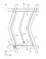
図2Aは、本発明の一実施形態に係る表示装置の選択トランジスタ領域及び画素領域を示す平面図である。図2Aに示すように、画素500は、第1方向D1に延在するゲート線531と、第1方向D1に交差する第2方向D2に延在するデータ線541と、ゲート線531及びデータ線541のクロスポイント539に配置された選択トランジスタ510と、選択トランジスタ510を介してデータ線541に接続された画素電極520とを有する。また、図示していないが、選択トランジスタ510と画素電極520との間に保持容量が配置されていてもよい。[Pixel Layout of Display Device 10]
FIG. 2A is a plan view showing a selection transistor region and a pixel region of a display device according to an embodiment of the present invention. As shown in FIG. 2A, the
図2Aでは、ゲート線531及びデータ線541は平面視においてそれぞれ直線形状であり、互いに直交するレイアウトが例示されているが、このレイアウトに限定されない。例えば、ゲート線531及びデータ線541の両方又は一方は屈曲しながら第1方向D1又は第2方向D2に延在してもよい。また、クロスポイント539において、ゲート線531とデータ線541とは90度以外の角度で交差してもよい。 In FIG. 2A, the
また、図2Aでは、画素電極520は一部の領域を除いてゲート線531とデータ線541との間にオフセットが設けられたレイアウト、つまり、平面視において、画素電極520は一部の領域を除いてゲート線531及びデータ線541と重畳しないレイアウトが例示されているが、このレイアウトに限定されない。例えば、平面視において画素電極520の外周端部がゲート線531及びデータ線541と重畳していてもよい。 In FIG. 2A, the
図2Aに示す表示装置10では、選択トランジスタ510のオン/オフはゲート線531に供給されるゲート電圧によって制御される。つまり、ゲート線531に所定のゲート電圧が印加されることで、選択トランジスタ510がオン状態となり、データ線541と画素電極520とを接続する。選択トランジスタ510がオン状態になることで、データ線541に供給された画素の階調に対応するデータ信号は選択トランジスタ510を介して画素電極520に供給される。 In the
また、図示しないが、画素電極520が配置された基板に対向して設けられ、当該基板と共に液晶材料を挟持する対向基板にはコモン電圧が印加されるコモン電極が形成されている。つまり、表示装置10において、液晶材料は画素電極520とコモン電極との間に生成された縦方向(基板100のトランジスタ等が形成された面に対して垂直な方向)電界によって配向される。 Although not shown, a common electrode to which a common voltage is applied is formed on a counter substrate which is provided facing the substrate on which the
[表示装置10の構造]
次に、選択トランジスタ510及び画素電極520の構造について、平面図及び断面図を用いて詳細に説明する。ここで、実施形態1の選択トランジスタ510として、チャネルとして酸化物半導体を用いた構造を例示するが、この構造に限定されず、チャネルとしてシリコンなどの半導体やGa−As等の化合物半導体、ペンタセン又はテトラシアノキノジメタン(TCNQ)等の有機半導体を用いることもできる。[Structure of Display Device 10]
Next, structures of the
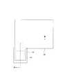
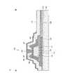
図2Bは、本発明の一実施形態に係る表示装置の選択トランジスタ領域及び画素領域の拡大図を示す平面図である。また、図3は、本発明の一実施形態に係る表示装置の選択トランジスタ領域及び画素領域のA−B断面図である。まず、断面図を用いて表示装置10の構造を説明する。図3に示すように、表示装置10は、基板100と、基板100上に配置された下地層110と、下地層110上に配置された下部電極120(第2電極)と、下部電極120上及び下地層110上に配置された第1透明導電層115と、第1透明導電層115上に配置され、パターン端部に第1側壁131を有する第1絶縁層130と、第1絶縁層130の上面に配置された補助電極190(第3電極)と、を有する。 FIG. 2B is a plan view showing an enlarged view of the selection transistor region and the pixel region of the display device according to the embodiment of the present invention. FIG. 3 is a cross-sectional view taken along the line AB of the selection transistor region and the pixel region of the display device according to the embodiment of the present invention. First, the structure of the
また、表示装置10は、第1側壁131上、補助電極190上及び第1透明導電層115上に配置された酸化物半導体層140と、第1側壁131に配置された酸化物半導体層140に対向して設けられたゲート電極160と、酸化物半導体層140とゲート電極160との間に配置されたゲート絶縁層150と、を有する。ここで、第1透明導電層115は、酸化物半導体層140と基板100との間に配置され、第1領域132において酸化物半導体層140の一方に接続されている。さらに、表示装置10は、第1絶縁層130の基板100とは反対側に配置され、第2領域182において酸化物半導体層140の他方に接続された上部電極180(第1電極)と、第1透明導電層115に接続され、第1透明導電層115と同一層の画素電極520(第2透明導電層)と、を有する。 The
ここで、ゲート電極160上には層間絶縁層170(第3絶縁層)が配置されており、一部の領域においてゲート電極160と上部電極180とを隔離する。上部電極180は層間絶縁層170に設けられた開口部171を介して酸化物半導体層140に接続されている。 Here, an interlayer insulating layer 170 (third insulating layer) is disposed on the
下部電極120は、基板100と第1透明導電層115との間に配置されており、第1領域132において第1透明導電層115を介して酸化物半導体層140の一方に接続されている。また、図2Bに示すように、下部電極120は、データ線541の延在方向と同じ方向に延在している。ただし、第1透明導電層115及び画素電極520が画素の表示に影響を及ぼさない程度に十分に低い導電率を有している場合は、下部電極120はゲート線531及びデータ線541のクロスポイント539の領域だけに配置されていてもよい。また、第1透明導電層115及び画素電極520がさらに低い導電率を有している場合は、下部電極120を省略することができる。 The
図3に示すように、第1絶縁層130の第1側壁131は傾斜面が上方を向くテーパ形状である。また、第1絶縁層130は、図2Bの斜線部(チャネル領域141)の外周をパターン端部とするパターン形状で配置されている。また、第1絶縁層130のパターン端部に設けられた第1側壁131は、図2Bの斜線部(チャネル領域141)のように、当該パターンの外周に沿って環状に設けられている。 As shown in FIG. 3, the
図2Bに示すように、ゲート電極160はゲート線531の一部であり、上部電極180はデータ線541の一部である。換言すると、ゲート電極160はゲート線531に含まれ、上部電極180はデータ線541に含まれる。 As shown in FIG. 2B, the
次に、上記で説明したトランジスタに含まれる各層の形状及び材料について、より詳細に説明する。 Next, the shape and material of each layer included in the transistor described above will be described in more detail.
基板100は、ガラス基板を使用することができる。また、ガラス基板の他にも、石英基板、サファイア基板、樹脂基板などの透光性を有する絶縁基板を使用することができる。また、折り曲げ可能な表示装置(フレキシブルディスプレイ)の場合は、基板100として可撓性を有する基板を使用することができる。可撓性を有する基板としては、樹脂基板を使用することができる。樹脂基板としては、例えば、ポリイミド樹脂、アクリル樹脂、エポキシ樹脂などの材料を使用することができる。また、これらの材料に基板の耐熱性を向上させる不純物が混入された樹脂基板を使用することができる。 As the
下地層110としては、基板100からの不純物が酸化物半導体層140に拡散することを抑制することができる材料を使用することができる。例えば、下地層110として、窒化シリコン(SiNx)、窒化酸化シリコン(SiNxOy)、酸化シリコン(SiOx)、酸化窒化シリコン(SiOxNy)、窒化アルミニウム(AlNx)、窒化酸化アルミニウム(AlNxOy)、酸化アルミニウム(AlOx)、酸化窒化アルミニウム(AlOxNy)などを使用することができる(x、yは任意)。また、これらの膜を積層した構造を使用してもよい。As the
ここで、SiOxNyとは、酸素(O)よりも少ない量の窒素(N)を含有するシリコン化合物であり、AlOxNyとは、酸素(O)よりも少ない量の窒素(N)を含有するアルミニウム化合物である。また、SiNxOyとは、窒素よりも少ない量の酸素を含有するシリコン化合物であり、AlNxOyとは、窒素よりも少ない量の酸素を含有するアルミニウム化合物である。Here, SiOx Ny is a silicon compound containing nitrogen (N) in a smaller amount than oxygen (O), and AlOx Ny is nitrogen (N in a smaller amount than oxygen (O)). ) Containing an aluminum compound. Further, SiNx Oy is a silicon compound containing an amount of oxygen smaller than nitrogen, and AlNx Oy is an aluminum compound containing an amount of oxygen smaller than nitrogen.
上記に例示した下地層110は、ナノメートルオーダーで膜厚を制御可能な薄膜によって形成されている。膜厚をナノメートルオーダーで制御可能な薄膜としては、物理蒸着法(Physical Vapor Deposition:PVD法)又は化学蒸着法(Chemical Vapor Deposition:CVD法)によって成膜された薄膜を用いることができる。ここで、PVD法とは、スパッタリング法、真空蒸着法、電子ビーム蒸着法、めっき法、及び分子線エピタキシー法などを用いた成膜方法である。また、CVD法とは、熱CVD法、プラズマCVD法、触媒CVD法(Cat(Catalytic)−CVD法又はホットワイヤCVD法)などを用いた成膜方法である。また、ナノメートルオーダー(1μm未満の範囲)で膜厚を制御することができれば、上記に例示した蒸着法以外の方法を用いて成膜した薄膜であってもよい。 The
下部電極120は、一般的な金属材料又は導電性材料を使用することができる。例えば、アルミニウム(Al)、チタン(Ti)、クロム(Cr)、コバルト(Co)、ニッケル(Ni)、亜鉛(Zn)、モリブデン(Mo)、インジウム(In)、スズ(Sn)、ハフニウム(Hf)、タンタル(Ta)、タングステン(W)、白金(Pt)、ビスマス(Bi)などを使用することができる。また、これらの材料の合金を使用してもよい。また、これらの材料の窒化物を使用してもよい。また、ITO(酸化インジウム・スズ)、IGO(酸化インジウム・ガリウム)、IZO(酸化インジウム・亜鉛)、GZO(ガリウムがドーパントとして添加された酸化亜鉛)等の導電性酸化物を使用してもよい。また、これらの膜を積層した構造を使用してもよい。下部電極120も、下地層110と同様にナノメートルオーダーで膜厚を制御可能な薄膜によって形成することができる。 The
ここで、下部電極120として使用する材料は、酸化物半導体をチャネルに用いたトランジスタを有する表示装置の製造工程における熱処理工程に対して耐熱性を有し、その上層に配置される第1透明導電層115との接触抵抗が低い材料を使用することが好ましい。ここで、下部電極120上に第1透明導電層115を成膜する場合、下部電極120表面は酸素雰囲気に曝される。したがって、第1透明導電層115と良好な電気的接触を得るためには、少なくとも下部電極120の最表面が酸化しにくい材料を用いるとよい。又は、少なくとも下部電極120の最表面が酸化しても高抵抗化しにくい材料を用いるとよい。 Here, the material used as the
第1透明導電層115及び画素電極520は、一般的な透光性を有する導電性材料を使用することができる。例えば、ITO(酸化インジウム・スズ)、IGO(酸化インジウム・ガリウム)、IZO(酸化インジウム・亜鉛)、ZnO(酸化亜鉛)、SnO2(酸化スズ)、In2O3(酸化インジウム)、GZO(ガリウムがドーパントとして添加された酸化亜鉛)、ニオブ(Nb)などの不純物がドーパントとして添加された酸化チタン等の導電性酸化物を使用してもよい。また、これらの膜を積層した構造を使用してもよい。For the first transparent
第1絶縁層130は、下地層110と同様に、SiOx、SiNx、SiOxNy、SiNxOy、AlOx、AlNx、AlOxNy、AlNxOyなどの無機絶縁材料や、ポリイミド樹脂、アクリル樹脂、エポキシ樹脂、シリコーン樹脂、フッ素樹脂、シロキサン樹脂などの有機絶縁材料を用いることができる。また、第1絶縁層130は、ナノメートルオーダーで膜厚を制御可能な薄膜によって形成されており、下地層110と同様の方法で形成された薄膜を用いることができる。第1絶縁層130と下地層110とは同じ材料を用いてもよく、異なる材料を用いてもよい。Similar to the
また、図3では、第1絶縁層130の第1側壁131の断面形状が直線状の順テーパ形状である構造を例示したが、この構造に限定されず、第1側壁131の形状が上方に向かって凸形状の順テーパ形状であってもよく、逆に上方に向かって凹形状の順テーパ形状であってもよい。一方、第1側壁131の傾斜面は上方を向いた順テーパ形状に限定されず、垂直形状であってもよく、又は傾斜面が下方を向いた逆テーパ形状であってもよい。 3 illustrates a structure in which the cross-sectional shape of the
また、図3では、第1絶縁層130が単層である構造を例示したが、この構造に限定されず、複数の異なる層が積層された構造であってもよい。この場合、異なる層によって第1側壁131のテーパ角及び形状が異なっていてもよい。また、第1絶縁層130として、異なる物性の層(例えば、SiNx及びSiOx)を積層させることで、第1側壁131の場所によって特性が異なる酸化物半導体層140が形成されるようにしてもよい。つまり、表示装置10のトランジスタは、特性が異なる酸化物半導体層140が直列に接続されたチャネルを有していてもよい。3 illustrates the structure in which the first insulating
酸化物半導体層140は、半導体の特性を有する酸化金属を用いることができる。例えば、インジウム(In)、ガリウム(Ga)、亜鉛(Zn)、及び酸素(O)を含む酸化物半導体を用いることができる。特に、In:Ga:Zn:O=1:1:1:4の組成比を有する酸化物半導体を用いることができる。ただし、本発明に使用されIn、Ga、Zn、及びOを含む酸化物半導体は上記の組成に限定されるものではなく、上記とは異なる組成の酸化物半導体を用いることもできる。例えば、移動度を向上させるためにInの比率を大きくしてもよい。また、バンドギャップを大きくし、光照射による影響を小さくするためにGaの比率を大きくしてもよい。また、酸化物半導体層140は、ナノメートルオーダーで膜厚を制御可能な薄膜によって形成することができる。 The
また、In、Ga、Zn、及びOを含む酸化物半導体に他の元素が添加されていてもよく、例えばAl、Snなどの金属元素が添加されていてもよい。また、上記の酸化物半導体以外にも酸化亜鉛(ZnO)、酸化ニッケル(NiO)、酸化スズ(SnO2)、酸化チタン(TiO2)、酸化バナジウム(VO2)、酸化インジウム(In2O3)、チタン酸ストロンチウム(SrTiO3)などを用いることができる。なお、酸化物半導体層140はアモルファスであってもよく、結晶性であってもよい。また、酸化物半導体層140はアモルファスと結晶の混相であってもよい。In addition, another element may be added to the oxide semiconductor containing In, Ga, Zn, and O. For example, a metal element such as Al or Sn may be added. In addition to the above oxide semiconductors, zinc oxide (ZnO), nickel oxide (NiO), tin oxide (SnO2 ), titanium oxide (TiO2 ), vanadium oxide (VO2 ), indium oxide (In2 O3) ), Strontium titanate (SrTiO3 ), or the like. Note that the
ゲート絶縁層150は、下地層110及び第1絶縁層130と同様に、SiOx、SiNx、SiOxNy、SiNxOy、AlOx、AlNx、AlOxNy、AlNxOyなどの無機絶縁材料を用いることができる。また、ゲート絶縁層150は、ナノメートルオーダーで膜厚を制御可能な薄膜によって形成されており、下地層110と同様の方法で形成した薄膜を用いることができる。また、ゲート絶縁層150はこれらの絶縁層を積層した構造を使用することができる。ゲート絶縁層150は、下地層110及び第1絶縁層130と同じ材料であってもよく、異なる材料であってもよい。Similarly to the
ゲート電極160は、下部電極120と同様の材料を用いることができる。ゲート電極160は下部電極120と同じ材料を用いてもよく、異なる材料を用いてもよい。ゲート電極160として使用する材料は、酸化物半導体をチャネルに用いたトランジスタの製造工程における熱処理工程に対して耐熱性を有し、ゲート電極が0Vのときにトランジスタがオフするエンハンスメント型となる仕事関数を有する材料を用いることが好ましい。ゲート電極160はナノメートルオーダーで膜厚を制御可能な薄膜によって形成することができる。図3では、ゲート電極160が単層である構造を例示したが、この構造に限定されず、複数の異なる層が積層された構造であってもよい。 The
層間絶縁層170は、下地層110、第1絶縁層130、及びゲート絶縁層150と同様に、SiOx、SiNx、SiOxNy、SiNxOy、AlOx、AlNx、AlOxNy、AlNxOyなどの無機絶縁材料を用いることができる。また、層間絶縁層170は、ナノメートルオーダーで膜厚を制御可能な薄膜によって形成されており、下地層110と同様の方法でした薄膜を用いることができる。層間絶縁層170としては、上記の無機絶縁材料の他にTEOS層や有機絶縁材料を用いることができる。ここで、TEOS層とはTEOS(Tetra Ethyl Ortho Silicate)を原料としたCVD層を指すもので、下地の段差を緩和して平坦化する効果を有する膜である。また、有機絶縁材料としては、ポリイミド樹脂、アクリル樹脂、エポキシ樹脂、シリコーン樹脂、フッ素樹脂、シロキサン樹脂などを用いることができる。層間絶縁層170は、上記の材料を単層で用いてもよく、積層させてもよい。例えば、無機絶縁材料及び有機絶縁材料を積層させてもよい。Similar to the
上部電極180は、下部電極120及びゲート電極160と同様の材料を用いることができる。上部電極180は下部電極120及びゲート電極160と同じ材料を用いてもよく、異なる材料を用いてもよい。また、上部電極180は、下部電極120及びゲート電極160として列挙した材料以外に銅(Cu)、銀(Ag)、金(Au)などを用いることもできる。上部電極180はナノメートルオーダーで膜厚を制御可能な薄膜によって形成した薄膜を用いることができる。 The
上部電極180として使用する材料は、酸化物半導体をチャネルに用いたトランジスタの製造工程における熱処理工程に対して耐熱性を有し、酸化物半導体層140との接触抵抗が低い材料を使用することが好ましい。ここで、酸化物半導体層140と良好な電気的接触を得るために、上部電極180として仕事関数が酸化物半導体層140より小さい金属材料を用いることができる。 The material used for the
[表示装置10の動作]
図2B及び図3に示す表示装置10を用いて、画素を駆動する動作について説明する。図2Bに示すように、表示装置10はゲート線531、データ線541、選択トランジスタ510、及び画素電極520を有する。ここで、選択トランジスタ510は酸化物半導体層140をチャネルとするトランジスタである。また、ゲート線531はゲート電極160に接続されている。また、データ線541は上部電極180に接続されている。また、画素電極520は選択トランジスタ510のドレイン側に接続されており、選択トランジスタ510がオン状態になることで選択トランジスタ510を介してデータ線541に接続される。[Operation of Display Device 10]
An operation of driving a pixel will be described using the
まず、ゲート線531に選択トランジスタ510をオン状態にするゲート電圧が印加されることで、ゲート電極160にもゲート電圧が印加される。そして、ゲート電極160に印加されたゲート電圧に基づき、ゲート絶縁層150を介して酸化物半導体層140に電界が生成されることで、第1側壁131に配置された酸化物半導体層140にチャネルが形成される。ここで、第1側壁131は環状に設けられているため、図2Bに示すように、環状のチャネル領域141が形成される。ここで、図2Bに示す選択トランジスタ510は、そのチャネル領域が環状に形成されていることから、当該構成を「サラウンド型」又は「サラウンド型トランジスタ」という。 First, the gate voltage is applied to the
チャネル領域141が形成された状態でデータ線541にデータ信号が印加されると、上部電極180、チャネル領域141、第1透明導電層115、及び下部電極120を介してデータ信号が画素電極520に供給される。つまり、上部電極180はソース電極として機能し、第1透明導電層115及び下部電極120はドレイン電極として機能する。そして、ゲート線531に印加されていたゲート電圧が選択トランジスタ510をオフ状態にする電圧に変化することで、選択トランジスタ510はオフ状態になり、画素電極520はデータ信号が供給された状態に保たれる。画素電極520と対向基板に設けられたコモン電極との間には、これらの電極間の電位差に基づいた電界が形成され、液晶材料が配向される。 When a data signal is applied to the
つまり、表示装置10において、選択トランジスタ510のゲート電極160、ソース電極として機能する上部電極180、及びドレイン電極として機能する下部電極120(又は第1透明導電層115)は、平面視において、ゲート線531又はデータ線541と重畳する領域に配置することができる。より具体的には、選択トランジスタ510は、ゲート線531とデータ線541とが交差する領域、つまりクロスポイント539を含む領域に形成することができる。 That is, in the
ここで、酸化物半導体層140をチャネルに用いた選択トランジスタ510はオフ電流が非常に小さいため、画素電極520に供給されたデータ信号は次のフレームのデータ信号供給まで維持されるが、必要に応じて画素電極520に供給されたデータ信号を保持するための保持容量が設けられてもよい。また、図2B及び図3では、平面視においてゲート電極160と重畳しない領域にも酸化物半導体層140が配置された構造を例示したが、この構造に限定されず、平面視においてゲート電極160と重畳しない領域には酸化物半導体層140が配置されない構造であってもよい。 Here, since the off-state current of the
上記のように、表示装置10において、第1側壁131に配置された酸化物半導体層140がチャネルとして機能する。したがって、表示装置10におけるチャネル長は第1絶縁層130の膜厚及び第1側壁131のテーパ角によって制御される。 As described above, in the
以上のように、本発明の実施形態1に係る表示装置10によると、第1絶縁層130の第1側壁131に配置された酸化物半導体層140がチャネルとなるため、第1絶縁層130の膜厚及び第1側壁131のテーパ角の両方又は一方を制御することによって、選択トランジスタ510のチャネル長を制御することができる。上記のように、第1絶縁層130は、ナノメートルオーダーで膜厚を制御可能な薄膜によって形成されているため、ばらつきのオーダーがマイクロメートルオーダーであるフォトリソグラフィのパターニング限界よりも小さいチャネル長を有するトランジスタを実現することが可能となる。その結果、オン電流を向上させることができるトランジスタを有する表示装置を提供することができる。 As described above, according to the
また、本発明の実施形態1に係る表示装置10によると、選択トランジスタ510をゲート線531とデータ線541とが交差するクロスポイント539に配置することができるため、画素の開口率が高い表示装置を提供することができる。また、データ線541が延在する方向に沿って第1透明導電層115の下層に下部電極120が配置されることで、第2方向D2の配線抵抗を下げることができ、画素電極520の全域に効率よくデータ信号を供給することができる。また、補助電極190が第1絶縁層130と酸化物半導体層140との間に配置されることで、選択トランジスタ510のオン抵抗をより低減することができる。 In addition, according to the
また、本発明の実施形態1に係る表示装置10によると、環状の第1側壁131に対して酸化物半導体層140が配置され、チャネル領域141が環状に形成されているため、酸化物半導体層140のパターン端部がチャネル領域141に含まれない。酸化物半導体層140のパターン端部は、酸化物半導体層140のエッチングの際に物性が変化してしまうことがあるが、表示装置10では、酸化物半導体層140のパターン端部がチャネル領域141に含まれないため、酸化物半導体層140のパターン端部に起因したリークパスは発生しない。つまり、オフ電流がさらに少ないトランジスタを有する表示装置を実現することができる。 Further, according to the
また、本発明の実施形態1に係る表示装置10によると、第1絶縁層130の膜厚は上記のようにPVD法又はCVD法が用いられ、ナノメートルオーダーで制御することが可能であるため、膜厚の基板面内ばらつきもナノメートルオーダーに制御することができる。また、第1側壁131のテーパ角は、第1絶縁層130のエッチングレート及びレジストの後退量によって制御され、これらのばらつき制御も第1絶縁層130の膜厚ばらつきと同等のオーダーで制御することが可能である。したがって、第1絶縁層130の膜厚及びテーパ角の基板面内のばらつきは、フォトリソグラフィによるパターニングの基板面内のばらつきに比べて小さくすることができる。その結果、チャネル長の基板面内ばらつきを抑制することができるトランジスタを有する表示装置を実現することができる。 Further, according to the
また、本発明の実施形態1に係る表示装置10によると、第1側壁131の傾斜面がテーパ形状であることで、第1側壁131に対する酸化物半導体層140及びゲート絶縁層150の被覆性(カバレッジ)が向上する。したがって、第1側壁131に形成される酸化物半導体層140及びゲート絶縁層150の膜厚の制御性が良くなる。その結果、特性ばらつきが少ないトランジスタを有する表示装置を得ることができる。 In addition, according to the
[表示装置10の製造方法]
図4乃至図14を用いて、本発明の一実施形態に係る表示装置の製造方法について、平面図及び断面図を参照しながら説明する。[Manufacturing Method of Display Device 10]
A method for manufacturing a display device according to an embodiment of the present invention will be described with reference to FIGS.
図4は、本発明の一実施形態に係る表示装置の製造方法において、基板上に下地層及び下部電極を形成する工程を示す平面図である。図5は、本発明の一実施形態に係る表示装置の製造方法において、基板上に下地層及び下部電極を形成する工程を示す断面図である。図5に示すように、基板100上に下地層110及び下部電極120を成膜し、フォトリソグラフィ及びエッチングによって図4に示す下部電極120のパターンを形成する。ここで、下部電極120のエッチングは、下部電極120のエッチングレートと下地層110のエッチングレートとの選択比が大きい条件で処理することが好ましい。 FIG. 4 is a plan view showing a process of forming a base layer and a lower electrode on a substrate in the method for manufacturing a display device according to the embodiment of the present invention. FIG. 5 is a cross-sectional view illustrating a process of forming a base layer and a lower electrode on a substrate in a method for manufacturing a display device according to an embodiment of the present invention. As shown in FIG. 5, a
図6は、本発明の一実施形態に係る表示装置の製造方法において、第1透明導電層及び画素電極を形成する工程を示す断面図である。この工程における平面図は図4と同様なので、ここでは省略する。図6に示すように、下部電極120上及び下地層110上に第1透明導電層115及び画素電極520を成膜する。ここで、第1透明導電層115と下部電極120との接触抵抗を下げるために、第1透明導電層115の成膜前に下部電極120表面の自然酸化膜や有機汚染物を除去する工程を設けてもよい。 FIG. 6 is a cross-sectional view illustrating a process of forming the first transparent conductive layer and the pixel electrode in the method for manufacturing a display device according to the embodiment of the present invention. The plan view in this step is the same as that in FIG. As shown in FIG. 6, the first transparent
上記の除去工程は、第1透明導電層115及び画素電極520の成膜工程とは別の工程で、第1透明導電層115及び画素電極520の成膜装置とは別の装置で行われてもよい。一方、当該除去工程は、第1透明導電層115及び画素電極520の成膜工程と同じ工程で、第1透明導電層115及び画素電極520の成膜装置内で行われてもよい。当該除去工程として、例えば第1透明導電層115及び画素電極520の成膜装置内で逆スパッタなどを行うことができる。 The removal process is performed separately from the film formation process of the first transparent
図7は、本発明の一実施形態に係る表示装置の製造方法において、第1絶縁層及び補助電極を形成する工程を示す平面図である。図8は、本発明の一実施形態に係る表示装置の製造方法において、第1絶縁層及び補助電極を形成する工程を示す断面図である。図8に示すように、図6に示す基板の全面に第1絶縁層130及び補助電極190を成膜し、フォトリソグラフィ及びエッチングによって図7に示す第1絶縁層130及び補助電極190のパターンを形成する。 FIG. 7 is a plan view showing a process of forming the first insulating layer and the auxiliary electrode in the method for manufacturing a display device according to the embodiment of the present invention. FIG. 8 is a cross-sectional view illustrating a process of forming the first insulating layer and the auxiliary electrode in the method for manufacturing a display device according to the embodiment of the present invention. As shown in FIG. 8, the first insulating
ここで、第1絶縁層130及び補助電極190は一括でエッチングしてもよく、それぞれを別の工程でエッチングしてもよい。例えば、第1絶縁層130のパターンを形成した後に補助電極190を第1絶縁層130の上面及び側壁に成膜し、フォトリソグラフィ及びエッチングによって補助電極190のパターンを形成してもよい。第1絶縁層130のエッチングにおいて、第1透明導電層115及び画素電極520を当該エッチングのエッチングストッパとして利用することができる。 Here, the first insulating
第1絶縁層130のエッチングは、第1絶縁層130のエッチングレートと第1透明導電層115及び画素電極520のエッチングレートとの選択比が大きい条件で処理すればよい。例えば、第1透明導電層115及び画素電極520としてITOを用いた場合、ITOをエッチングできるエッチング条件は限られているため、第1絶縁層130のエッチング条件として多様な条件を用いることができる。 The etching of the first insulating
また、第1透明導電層115及び画素電極520を第1絶縁層130のエッチングストッパとして用いることができるため、例えば、第1絶縁層130及び下地層110を同じ材料で形成することもできる。また、図7では、第1絶縁層130は方形のパターンであるが、このパターン形状に限定されず、例えば、円形、楕円形、多角形、湾曲形など多様な形状であってもよい。 In addition, since the first transparent
ここで、第1絶縁層130の第1側壁131をテーパ形状にするためのエッチング方法について説明する。第1側壁131のテーパ角は、第1絶縁層130のエッチングレートと第1絶縁層130をエッチングする際にマスクとして用いるレジストの水平方向のエッチングレート(以下、レジストの後退量という)とによって制御することができる。例えば、第1絶縁層130のエッチングレートに比べてレジストの後退量が小さい場合、第1側壁131のテーパ角は大きく(垂直に近い角度)なり、レジストの後退量がゼロの場合は、第1側壁131は垂直となる。一方、第1絶縁層130のエッチングレートに比べてレジストの後退量が大きい場合、第1側壁131のテーパ角は小さく(緩やかな傾斜)なる。ここで、レジストの後退量はレジストパターン端部のテーパ角やレジストのエッチングレートによって調整することができる。 Here, an etching method for forming the
図9は、本発明の一実施形態に係る表示装置の製造方法において、酸化物半導体層を形成する工程を示す平面図である。図10は、本発明の一実施形態に係る表示装置の製造方法において、酸化物半導体層を形成する工程を示す断面図である。図10に示すように、図8に示す基板の全面に酸化物半導体層140を成膜し、フォトリソグラフィ及びエッチングによって図9に示す酸化物半導体層140のパターンを形成する。酸化物半導体層140はスパッタリング法を用いて成膜することができる。酸化物半導体層140は、少なくとも第1絶縁層130のパターン外周に沿って環状に設けられた第1側壁131を覆うように形成されていればよい。 FIG. 9 is a plan view showing a step of forming an oxide semiconductor layer in the method for manufacturing a display device according to the embodiment of the present invention. FIG. 10 is a cross-sectional view showing a step of forming an oxide semiconductor layer in the method for manufacturing a display device according to the embodiment of the present invention. As shown in FIG. 10, an
また、図10に示すように、酸化物半導体層140のエッチングと同じエッチング工程で第1透明導電層115をエッチングすることができる。酸化物半導体層140のエッチングはドライエッチングで行ってもよく、ウェットエッチングで行ってもよい。ウェットエッチングで酸化物半導体層140をエッチングする場合、シュウ酸を含むエッチャントを用いることができる。 In addition, as illustrated in FIG. 10, the first transparent
ここで、酸化物半導体層140は第1側壁131の全域に形成された構成を例示したが、この構成に限定されず、例えば第1側壁131の一部分のみを覆うような形状であってもよい。第1側壁131に酸化物半導体層140が形成されていない箇所が存在してもよい。また、図10では、画素電極520上の酸化物半導体層140を除去しない製造方法を例示したが、この製造方法に限定されず、画素電極520上の酸化物半導体層140を除去してもよい。 Here, the configuration in which the
図11は、本発明の一実施形態に係る表示装置の製造方法において、ゲート絶縁層及びゲート電極を形成する工程を示す平面図である。図12は、本発明の一実施形態に係る表示装置の製造方法において、ゲート絶縁層及びゲート電極を形成する工程を示す断面図である。図12に示すように、図10に示す基板の全面にゲート絶縁層150及びゲート電極160を形成し、フォトリソグラフィ及びエッチングによって図11に示すゲート電極160のパターンを形成する。ここで、図11に示すように、平面視において、ゲート電極160は環状の第1側壁131を覆うように配置されている。 FIG. 11 is a plan view showing a process of forming a gate insulating layer and a gate electrode in the method for manufacturing a display device according to the embodiment of the present invention. FIG. 12 is a cross-sectional view illustrating a process of forming a gate insulating layer and a gate electrode in the method for manufacturing a display device according to an embodiment of the present invention. As shown in FIG. 12, a
ここで、図11及び図12に示すように、ゲート電極160は、第1絶縁層130及び補助電極190のパターンに対応する領域に開口部を有している。また、図12に示すように、ゲート絶縁層150はゲート電極160のエッチングストッパとして機能しており、図12ではゲート電極160だけがエッチングされた状態を示す。ただし、ゲート絶縁層150及びゲート電極160を一括でエッチングしてもよい。 Here, as shown in FIGS. 11 and 12, the
図13は、本発明の一実施形態に係る表示装置の製造方法において、層間絶縁層を形成し、層間絶縁層及びゲート絶縁層に開口部を形成する工程を示す平面図である。図14は、本発明の一実施形態に係る表示装置の製造方法において、層間絶縁層を形成し、層間絶縁層及びゲート絶縁層に開口部を形成する工程を示す断面図である。図14に示すように、図12に示す基板の全面に層間絶縁層170を成膜し、フォトリソグラフィ及びエッチングによって図13に示す開口部171のパターンを形成する。 FIG. 13 is a plan view showing a process of forming an interlayer insulating layer and forming openings in the interlayer insulating layer and the gate insulating layer in the method for manufacturing a display device according to the embodiment of the present invention. FIG. 14 is a cross-sectional view showing a process of forming an interlayer insulating layer and forming openings in the interlayer insulating layer and the gate insulating layer in the method for manufacturing a display device according to the embodiment of the present invention. As shown in FIG. 14, an
ここで、開口部171は、第1絶縁層130及び補助電極190の上方に形成された酸化物半導体層140を露出する。また、開口部171を形成するエッチング条件は、ゲート絶縁層150及び層間絶縁層170のエッチングレートと、酸化物半導体層140のエッチングレートとの高い選択比を確保するエッチング条件であることが好ましい。 Here, the
そして、図14に示す基板の全面に上部電極180を成膜し、図3に示すように上部電極180のパターンを形成する。上記に示す製造工程によって、図2B及び図3に示すような本発明の実施形態1に係る表示装置10を形成することができる。ここで、図3における第1側壁131に形成された酸化物半導体層140がチャネル領域141となる。つまり、図2Bにおいてチャネル領域141は酸化物半導体層140とゲート電極160とが重畳する領域に形成される。つまり、選択トランジスタ510のチャネル領域141は第1側壁131に沿って環状に形成され、チャネル領域141は酸化物半導体層140のパターン端部を含まないサラウンド型の構成となっている。 Then, an
以上のように、本発明の実施形態1に係る表示装置10の製造方法によると、下地層110の形成と第1絶縁層130の形成との間に第1透明導電層115を形成することで、第1絶縁層130のパターンを形成する際に、第1透明導電層115をエッチングストッパとして利用することができる。したがって、第1絶縁層130のエッチング条件や下地層110及び第1絶縁層130の材料などのプロセスマージンを広げることができる。 As described above, according to the method for manufacturing the
〈実施形態1の変形例1〉
図15を用いて、本発明の一実施形態の変形例について説明する。実施形態1の変形例1に係る表示装置11は、実施形態1で説明した表示装置10と類似している。以下の説明において、表示装置10と同じ構造及び機能を有する要素には同一の符号を付与し、詳細な説明は省略する。<Modification 1 of Embodiment 1>
A modification of one embodiment of the present invention will be described with reference to FIG. The
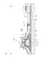
[表示装置11の構造]
図15は、本発明の一実施形態の変形例に係る表示装置の選択トランジスタ領域及び画素領域の断面図である。図15に示す表示装置11は図3に示す表示装置10と類似しているが、表示装置11は、画素電極520(第2透明導電層)が開口部175に配置された上部電極185を介して選択トランジスタ510の上部電極180(第1電極)に接続されている点、選択トランジスタ510の第1透明導電層115と画素電極520とが分離されている点において、表示装置10と相違する。[Structure of Display Device 11]
FIG. 15 is a cross-sectional view of a selection transistor region and a pixel region of a display device according to a modification of one embodiment of the present invention. The
つまり、表示装置11においては、上部電極180が選択トランジスタ510のドレイン電極として機能し、下部電極120がソース電極として機能する。したがって、データ線541は下部電極120と同一層によって形成され、下部電極120がデータ線541の一部となる。図15では、画素電極520上に酸化物半導体層140が配置された構造を例示したが、この構造に限定されず、画素電極520上に酸化物半導体層140が配置されておらず、上部電極185と画素電極520とが接触する構造であってもよい。 That is, in the
以上のように、本発明の実施形態1の変形例1に係る表示装置11によると、画素電極520が選択トランジスタ510の上部電極180に接続されていることで、選択トランジスタ510のドレイン電極である上部電極180から画素電極520までを上部電極180と同一層の配線で接続することができる。上部電極180として、透明導電層よりも抵抗の低い金属材料を用いることができるため、この構成によって、選択トランジスタ510と画素電極520との間の抵抗値を小さくすることができる。 As described above, according to the
〈実施形態1の変形例2〉
図16を用いて、本発明の一実施形態の変形例について説明する。実施形態1の変形例2に係る表示装置12は、実施形態1で説明した表示装置10と類似している。以下の説明において、表示装置10と同じ構造及び機能を有する要素には同一の符号を付与し、詳細な説明は省略する。<Modification 2 of Embodiment 1>
A modification of one embodiment of the present invention will be described with reference to FIG. The
[表示装置12の構造]
図16は、本発明の一実施形態の変形例に係る表示装置の選択トランジスタ領域及び画素領域の断面図である。図16に示す表示装置12は図3に示す表示装置10と類似しているが、表示装置12は、第1透明導電層115が下部電極120の下方に配置されている点において、表示装置10と相違する。表示装置12においては、表示装置10と同様に上部電極180が選択トランジスタ510のソース電極として機能し、下部電極120がドレイン電極として機能する。つまり、データ線541は上部電極180と同一層によって形成され、上部電極180がデータ線541の一部となる。[Structure of Display Device 12]
FIG. 16 is a cross-sectional view of a selection transistor region and a pixel region of a display device according to a modification of one embodiment of the present invention. The
以上のように、本発明の実施形態1の変形例2に係る表示装置12によると、表示装置10と同様の効果が得られる表示装置を提供することができる。また、酸化物半導体層140と下部電極120とを接触させることができるため、接触抵抗を低減させることができる。 As described above, according to the
[表示装置12の製造方法]
図17乃至図21を用いて、本発明の一実施形態の変形例に係る表示装置の製造方法について、平面図及び断面図を参照しながら説明する。なお、表示装置12の製造方法は図3に示す表示装置10の製造方法と類似しているため、詳細な説明は省略する。[Manufacturing Method of Display Device 12]
A method for manufacturing a display device according to a modification of one embodiment of the present invention will be described with reference to FIGS. 17 to 21 with reference to plan views and cross-sectional views. The manufacturing method of the
図17は、本発明の一実施形態の変形例に係る表示装置の製造方法において、基板上に下地層、第1透明導電層、画素電極、及び下部電極を形成する工程を示す断面図である。なお、この工程における平面図は図4と同様なので、ここでは省略する。図17に示すように、基板100上に下地層110、第1透明導電層115、画素電極520、及び下部電極120を成膜し、フォトリソグラフィ及びエッチングによって下部電極120のパターンを形成する。ここで、第1透明導電層115と下部電極120との接触抵抗を下げるために、下部電極120の成膜前に第1透明導電層115表面の有機汚染物を除去する工程を設けてもよい。また、下部電極120のエッチングにおいて、第1透明導電層115を当該エッチングのエッチングストッパとして利用することができる。 FIG. 17 is a cross-sectional view illustrating a process of forming a base layer, a first transparent conductive layer, a pixel electrode, and a lower electrode on a substrate in a method for manufacturing a display device according to a modification of one embodiment of the present invention. . Note that the plan view in this step is the same as that in FIG. As shown in FIG. 17, a
図18は、本発明の一実施形態の変形例に係る表示装置の製造方法において、第1絶縁層及び補助電極を形成する工程を示す断面図である。なお、この工程における平面図は図7と同様なので、ここでは省略する。図18に示すように、図17に示す基板の全面に第1絶縁層130及び補助電極190を成膜し、フォトリソグラフィ及びエッチングによって図7に示す第1絶縁層130のパターンを形成する。ここで、第1絶縁層130及び補助電極190は一括でエッチングしてもよく、それぞれを別の工程でエッチングしてもよい。例えば、第1絶縁層130をエッチングストッパとして補助電極190をエッチングし、下部電極120、第1透明導電層115、及び画素電極520をエッチングストッパとして第1絶縁層130をエッチングしてもよい。 FIG. 18 is a cross-sectional view illustrating a process of forming the first insulating layer and the auxiliary electrode in the method for manufacturing a display device according to the modification of the embodiment of the present invention. Note that a plan view in this step is the same as FIG. As shown in FIG. 18, the first insulating
図19は、本発明の一実施形態の変形例に係る表示装置の製造方法において、酸化物半導体層を形成する工程を示す断面図である。なお、この工程における平面図は図9と同様なので、ここでは省略する。図19に示すように、図18に示す基板の全面に酸化物半導体層140を成膜し、フォトリソグラフィ及びエッチングによって図9に示す酸化物半導体層140のパターンを形成する。また、酸化物半導体層140のエッチングと同じエッチング工程で露出された第1透明導電層115をエッチングすることができる。また、図19では、画素電極520上の酸化物半導体層140を除去しない製造方法を例示したが、この製造方法に限定されず、画素電極520上の酸化物半導体層140を除去してもよい。 FIG. 19 is a cross-sectional view showing a step of forming an oxide semiconductor layer in a method for manufacturing a display device according to a modification of one embodiment of the present invention. Note that a plan view in this step is the same as FIG. As shown in FIG. 19, an
図20は、本発明の一実施形態の変形例に係る表示装置の製造方法において、ゲート絶縁層及びゲート電極を形成する工程を示す断面図である。なお、この工程における平面図は図11と同様なので、ここでは省略する。図20に示すように、図19に示す基板の全面にゲート絶縁層150及びゲート電極160を形成し、フォトリソグラフィ及びエッチングによって図11に示すゲート電極160のパターンを形成する。図20では、ゲート絶縁層150がゲート電極160のエッチングストッパとなり、ゲート電極160だけがエッチングされた状態を示すが、ゲート絶縁層150及びゲート電極160を一括でエッチングしてもよい。 FIG. 20 is a cross-sectional view showing a process of forming a gate insulating layer and a gate electrode in a method for manufacturing a display device according to a modification of one embodiment of the present invention. Note that a plan view in this step is the same as FIG. As shown in FIG. 20, the
図21は、本発明の一実施形態の変形例に係る表示装置の製造方法において、層間絶縁層を形成し、層間絶縁層及びゲート絶縁層に開口部を形成する工程を示す断面図である。なお、この工程における平面図は図13と同様なので、ここでは省略する。図21に示すように、図20に示す基板の全面に層間絶縁層170を成膜し、フォトリソグラフィ及びエッチングによって図13に示す開口部171のパターンを形成する。ここで、開口部171は、第1絶縁層130及び補助電極190の上方に形成された酸化物半導体層140を露出する。 FIG. 21 is a cross-sectional view showing a process of forming an interlayer insulating layer and forming openings in the interlayer insulating layer and the gate insulating layer in the method for manufacturing a display device according to the modification of the embodiment of the present invention. Note that a plan view in this step is the same as FIG. As shown in FIG. 21, an
そして、図21に示す基板の全面に上部電極180を成膜し、図16に示すように上部電極180のパターンを形成する。上記に示す製造工程によって、図16に示すような本発明の実施形態1の変形例2に係る表示装置12を形成することができる。 Then, an
〈実施形態1の変形例3〉
図22を用いて、本発明の一実施形態の変形例について説明する。実施形態1の変形例3に係る表示装置13は、図16に示す表示装置12と類似している。以下の説明において、表示装置12と同じ構造及び機能を有する要素には同一の符号を付与し、詳細な説明は省略する。<Modification 3 of Embodiment 1>
A modification of one embodiment of the present invention will be described with reference to FIG. The
[表示装置13の構造]
図22は、本発明の一実施形態の変形例に係る表示装置の選択トランジスタ領域及び画素領域の断面図である。図22に示す表示装置13は図16に示す表示装置12と類似しているが、表示装置13は、画素電極520(第2透明導電層)が開口部175に配置された上部電極185を介して選択トランジスタ510の上部電極180(第1電極)に接続されている点、選択トランジスタ510の第1透明導電層115と画素電極520とが分離されている点において、表示装置12と相違する。[Structure of Display Device 13]
FIG. 22 is a cross-sectional view of a selection transistor region and a pixel region of a display device according to a modification of one embodiment of the present invention. The
つまり、表示装置13においては、上部電極180が選択トランジスタ510のドレイン電極として機能し、下部電極120がソース電極として機能する。したがって、データ線541は下部電極120と同一層によって形成され、下部電極120がデータ線541の一部となる。図22では、画素電極520上に酸化物半導体層140が配置された構造を例示したが、この構造に限定されず、画素電極520上に酸化物半導体層140が配置されておらず、上部電極185と画素電極520とが接触する構造であってもよい。 That is, in the
以上のように、本発明の実施形態1の変形例3に係る表示装置13によると、画素電極520が選択トランジスタ510の上部電極180に接続されていることで、選択トランジスタ510のドレイン電極である上部電極180から画素電極520までを上部電極180と同一層の配線で接続することができる。上部電極180として、透明導電層よりも抵抗の低い金属材料を用いることができるため、この構成によって、選択トランジスタ510と画素電極520との間の抵抗値を小さくすることができる。 As described above, according to the
〈実施形態1の変形例4〉
図23を用いて、本発明の一実施形態の変形例について説明する。実施形態1の変形例4に係る表示装置14は、実施形態1の変形例2で説明した表示装置12と類似している。以下の説明において、表示装置12と同じ構造及び機能を有する要素には同一の符号を付与し、詳細な説明は省略する。<Modification 4 of Embodiment 1>
A modification of the embodiment of the present invention will be described with reference to FIG. The
[表示装置14の構造]
図23は、本発明の一実施形態の変形例に係る表示装置の選択トランジスタ領域及び画素領域の断面図である。図23に示す表示装置14は図16に示す表示装置12と類似しているが、表示装置14は、下部電極120が配置されておらず、選択トランジスタ510のドレイン領域において酸化物半導体層140が第1透明導電層115に接続されている点において、表示装置12と相違する。[Structure of Display Device 14]
FIG. 23 is a cross-sectional view of a selection transistor region and a pixel region of a display device according to a modification of one embodiment of the present invention. The
以上のように、本発明の実施形態1の変形例4に係る表示装置14によると、表示装置12と同様の効果が得られる表示装置を提供することができ、さらに下部電極120を形成する工程を省略することができる。したがって、表示装置12に比べて表示装置14の工程数を短縮化することができるため、製造コストを低減することができる。 As described above, according to the
〈実施形態1の変形例5〉
図24Aを用いて、本発明の一実施形態の変形例について説明する。実施形態1の変形例5に係る表示装置15は、実施形態1で説明した表示装置10と類似している。以下の説明において、表示装置10と同じ構造及び機能を有する要素には同一の符号を付与し、詳細な説明は省略する。<Modification 5 of Embodiment 1>
A modification of one embodiment of the present invention will be described with reference to FIG. 24A. A
[表示装置15の構造]
図24Aは、本発明の一実施形態の変形例に係る表示装置の選択トランジスタ領域及び画素領域の断面図である。図24Aに示す表示装置15は図3に示す表示装置10と類似しているが、表示装置15は、上部電極180が酸化物半導体層140ではなく補助電極190に接触している点において、表示装置12と相違する。換言すると、表示装置15において、上部電極180は、補助電極190を介して酸化物半導体層140に接続されている。表示装置15では、酸化物半導体層140は補助電極190と接していればよく、酸化物半導体層140と上部電極180とが平面視において重畳している必要はない。つまり、図3の表示装置10とは異なり、上部電極180が酸化物半導体層140の上方に配置されていなくてもよい。[Structure of Display Device 15]
FIG. 24A is a cross-sectional view of a selection transistor region and a pixel region of a display device according to a modification of one embodiment of the present invention. The
以上のように、実施形態1の変形例5に係る表示装置15によると、上部電極180が補助電極190と接しているため、接触抵抗をより低くすることができる。その結果、オン電流を向上させることができるトランジスタを有する表示装置を提供することができる。 As described above, according to the
〈実施形態1の変形例6〉
図24Bを用いて、本発明の一実施形態の変形例について説明する。実施形態1の変形例6に係る表示装置16は、実施形態1で説明した表示装置10と類似している。以下の説明において、表示装置10と同じ構造及び機能を有する要素には同一の符号を付与し、詳細な説明は省略する。<Modification 6 of Embodiment 1>
A modification of one embodiment of the present invention will be described with reference to FIG. 24B. The
[表示装置16の構造]
図24Bは、本発明の一実施形態の変形例に係る表示装置の選択トランジスタ領域及び画素領域の断面図である。図24Bに示す表示装置16は図3に示す表示装置10と類似しているが、表示装置16は、第1絶縁層130の上方において、第1絶縁層130と酸化物半導体層140との間に補助電極190が設けられていない点において、図3に示す表示装置10と相違する。つまり、上部電極180は第1絶縁層130の上方において、酸化物半導体層140に接続されている。[Structure of Display Device 16]
FIG. 24B is a cross-sectional view of a selection transistor region and a pixel region of a display device according to a variation of one embodiment of the present invention. The
表示装置16では、ゲート電極160のパターン端部161と上部電極180のパターン端部181との間に、ゲート電極160に印加されたゲート電圧によって電界が形成されないオフセット領域が存在する。この構造は酸化物半導体層140の上部電極180側だけにオフセット領域が設けられた片側オフセット構造という。片側オフセット構造のトランジスタにおいて、オフセットが設けられた側の上部電極180にドレイン電圧を印加した場合、オフセット近傍の酸化物半導体層140中の電子は上部電極180のドレイン電圧の影響を受けるため電流が流れる。一方、上部電極180にソース電圧を印加した場合、オフセット近傍の酸化物半導体層140中の電子は下部電極120又は第1透明導電層115に印加されたドレイン電圧の影響をほとんど受けないため電流が流れない。つまり、片側オフセット構造のトランジスタは整流性を有し、ダイオード素子として利用することができる。 In the
一方、選択トランジスタ510のより高いオン電流を得るために、このオフセット領域にチャネルよりも導電率が高い酸化物半導体層140を設けてもよい。オフセット領域の導電率が高い酸化物半導体層140は、例えば、ゲート電極160のパターンを形成した工程の後に、ゲート電極160をマスクとして、上方から酸化物半導体層140にキャリアを生成する不純物を導入する、又は層間絶縁層170に水素を含有したSiNx等の無機絶縁膜を成膜することで実現することができる。On the other hand, in order to obtain a higher on-state current of the
以上のように、実施形態1の変形例6に係る表示装置16によると、第1絶縁層130の上方に補助電極190を形成する必要がないため、補助電極190を形成する工程を省略することができる。したがって、表示装置10に比べて表示装置16の工程数を短縮化することができるため、製造コストを低減することができる。また、第1絶縁層130の上方に補助電極190が配置されていないことで、第1絶縁層130の形状の調整を容易に行うことができる。 As described above, according to the
〈実施形態2〉
図25及び図26を用いて、本発明の一実施形態に係る画素レイアウト、及びその断面構造について説明する。実施形態2の表示装置20として、横電界方式の液晶表示装置のトランジスタアレイ基板について説明する。なお、表示装置20の概要については、実施形態1と同様であるので、ここでは説明を省略する。<Embodiment 2>
A pixel layout and a sectional structure thereof according to an embodiment of the present invention will be described with reference to FIGS. A transistor array substrate of a horizontal electric field type liquid crystal display device will be described as the
[表示装置20の画素レイアウト]
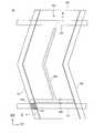
図25は、本発明の一実施形態に係る表示装置の選択トランジスタ領域及び画素領域を示す平面図である。図25に示すように、画素500は、第1方向D1に延在するゲート線531と、第1方向D1に交差する第2方向D2に屈曲しながら延在するデータ線541と、ゲート線531及びデータ線541のクロスポイント539に配置された選択トランジスタ510と、選択トランジスタ510を介してデータ線541に接続された画素電極520と、平面視において画素電極520に対向して配置され、第1方向D1に延在するコモン線551に接続されたコモン電極555(第3透明導電層)と、平面視において画素電極520と上部電極185とが重畳し、選択トランジスタ510及び画素電極520に接続された保持容量560と、を有する。[Pixel Layout of Display Device 20]
FIG. 25 is a plan view showing a selection transistor region and a pixel region of a display device according to an embodiment of the present invention. As shown in FIG. 25, the
図25に示すように、画素電極520及びコモン電極555は、データ線541に沿って屈曲しながら第2方向D2に延在している。また、保持容量560は、画素電極520の一部と、開口部175を介してコモン電極555に接続された上部電極185と、が平面視において重畳する領域に設けられている。また、コモン線551はクロスポイント539に配置された選択トランジスタ510を回避するように第1方向D1に延在している。 As shown in FIG. 25, the
ここで、図25では、画素電極520は隣接するデータ線541の両方に沿って2本配置され、2本の画素電極520の略中間に1本のコモン電極555が配置された構成を例示したが、この構成に限定されない。例えば、コモン電極555が隣接するデータ線541の両方に沿って2本配置され、2本のコモン電極555の略中間に1本の画素電極520が配置されてもよい。また、隣接するデータ線541に沿って配置された画素電極520及びコモン電極555の一方又は両方が3本以上であってもよい。 Here, FIG. 25 exemplifies a configuration in which two
図25では、データ線541、画素電極520、及びコモン電極555が屈曲しながら第2方向D2に延在する構成を例示したが、この構成に限定されず、データ線541、画素電極520、及びコモン電極555は直線形状で第2方向D2に延在する構成であってもよい。また、図25では、選択トランジスタ510及び画素電極520に保持容量560が接続された構成を例示したが、この構成に限定されない。例えば、選択トランジスタ510のオフ電流が、画素電極520に供給されたデータ信号を次のフレームのデータ信号供給まで維持することができる程度に十分に小さければ、保持容量560を省略することができる。 FIG. 25 illustrates a configuration in which the
図25に示す表示装置20では、ゲート線531にゲート電圧が印加されることで選択トランジスタ510がオン状態となる。そして、選択トランジスタ510がオン状態でデータ線541にデータ信号が印加されると、データ信号は選択トランジスタ510を介して画素電極520に供給される。一方、コモン電極555にはコモン線551を介してコモン電圧が印加されている。つまり、表示装置20において、画素電極520(第2透明導電層)及びコモン電極555(第3透明導電層)には異なる電圧が印加され、液晶材料は画素電極520とコモン電極555との間に生成された横方向(基板100のトランジスタ等が形成された面に対して水平な方向)電界によって配向される。 In the
[表示装置20の構造]
次に、選択トランジスタ510及び画素電極520の構造について、平面図及び断面図を用いて詳細に説明する。ここで、実施形態2の選択トランジスタ510及び画素電極520として、図3に示した実施形態1の選択トランジスタ510及び画素電極520と同様の構造を用いた場合について説明するが、実施形態1の変形例に示した選択トランジスタ及び画素電極と同様の構造を用いることもできる。また、実施形態2の選択トランジスタ510のチャネルとして酸化物半導体を用いた構造を例示するが、この構造に限定されず、チャネルとしてシリコンなどの半導体やGa−As等の化合物半導体、ペンタセン又はテトラシアノキノジメタン(TCNQ)等の有機半導体を用いることもできる。[Structure of Display Device 20]
Next, structures of the
図26は、本発明の一実施形態に係る表示装置の選択トランジスタ領域及び画素領域のC−D断面図である。図26に示す選択トランジスタ510の構造は図3に示す表示装置10の選択トランジスタ510と同じ構造なので、ここでは説明を省略する。図26に示すように、コモン線551及びコモン電極555は、第1透明導電層115及び画素電極520と同一層で形成されている。 FIG. 26 is a CD cross-sectional view of the selection transistor region and the pixel region of the display device according to the embodiment of the present invention. The structure of the
保持容量560は、画素電極520と、選択トランジスタ510の上部電極180と同一層で形成され、開口部175を介してコモン電極555に接続された上部電極185と、を一対の電極とする容量素子である。また、保持容量560は、画素電極520と上部電極185との間に配置されたゲート絶縁層150及び層間絶縁層170を誘電体とする容量素子である。図26に示した表示装置20では、保持容量560の画素電極520に対向する電極が上部電極180と同一層で形成された構造を例示したが、この構造に限定されない。例えば、保持容量560の画素電極520に対向する電極がゲート電極160と同一層で形成された構造であってもよい。つまり、保持容量560は、ゲート絶縁層150を誘電体とする容量素子であってもよい。 The
画素500の選択トランジスタ510に接続されたゲート線531に隣接するゲート線535は、第1絶縁層130と同一層で形成された層間絶縁層135によってコモン線551から離隔されている。 A
また、図26では、コモン電極555上に酸化物半導体層140が配置された構造を例示したが、この構造に限定されず、コモン電極555上に酸化物半導体層140が配置されておらず、上部電極185とコモン電極555とが接触する構造であってもよい。 FIG. 26 illustrates the structure in which the
以上のように、本発明の実施形態2に係る表示装置20によると、実施形態1に係る表示装置第10と同等の効果を得ることができ、さらに視野角が広い横電界方式の液晶表示装置を実現することができる。また、工程数を増加させることなく、保持容量560を形成することができる。また、ゲート線535とコモン線551との間に層間絶縁層135を配置することで、ゲート線535とコモン線551との間の寄生容量を低減することができる。したがって、画素回路駆動における信号遅延を抑制することができる。 As described above, according to the
〈実施形態3〉
図27及び図28を用いて、本発明の一実施形態に係る画素レイアウト、及びその断面構造について説明する。実施形態3の表示装置30として、横電界方式の液晶表示装置のトランジスタアレイ基板について説明する。なお、表示装置30の概要については、実施形態1と同様であるので、ここでは説明を省略する。<Embodiment 3>
A pixel layout and its cross-sectional structure according to an embodiment of the present invention will be described with reference to FIGS. A transistor array substrate of a horizontal electric field type liquid crystal display device will be described as the
[表示装置30の画素レイアウト]
図27は、本発明の一実施形態に係る表示装置の選択トランジスタ領域及び画素領域を示す平面図である。図27に示すように、画素500は、第1方向D1に延在するゲート線531と、第1方向D1に交差する第2方向D2に屈曲しながら延在するデータ線541と、ゲート線531及びデータ線541のクロスポイント539に配置された選択トランジスタ510と、選択トランジスタ510を介してデータ線541に接続された画素電極520と、データ線541に沿って屈曲しながら第2方向D2に延在し、平面視において画素電極520と重畳するように画素のほぼ全体に亘って配置されたコモン電極557と、平面視において画素電極520とコモン電極557とが重畳する領域に配置され、選択トランジスタ510及び画素電極520に接続された保持容量560とを有する。[Pixel Layout of Display Device 30]
FIG. 27 is a plan view showing a selection transistor region and a pixel region of a display device according to an embodiment of the present invention. As shown in FIG. 27, the
コモン電極557はマトリクス状に配置された画素において、第2方向D2に隣接する画素に共通して配置されている。また、図27では、平面視において、コモン電極557が画素のほぼ全体に亘って配置されることで画素電極520と重畳する構成を例示したが、この構成に限定されない。例えば、図25に示す表示装置20における画素電極520とコモン電極555との関係のように、コモン電極557は、屈曲しながら第2方向D2に延在する画素電極520を挟むように隣接するデータ線541に沿って2本配置されていてもよい。 In the pixels arranged in a matrix, the
つまり、コモン電極557は、平面視において、少なくとも画素電極520と異なる領域に配置され、画素500に横方向の電界が生成されるように配置されていればよい。また、保持容量を構成するために、平面視において一部の領域でコモン電極557と画素電極520とが重畳していてもよい。 In other words, the
図27に示すように、画素電極520は隣接するデータ線541の略中間に配置されており、隣接するデータ線541に沿って屈曲しながら第2方向D2に延在している。図27では、隣接するデータ線541に沿って配置された画素電極520が1本である構成を例示したが、画素電極520は隣接するデータ線541に沿って2本以上配置されていてもよい。 As shown in FIG. 27, the
図27では、データ線541、画素電極520、及びコモン電極557が屈曲しながら第2方向D2に延在する構成を例示したが、この構成に限定されず、データ線541、画素電極520、及びコモン電極557は直線形状で第2方向D2に延在する構成であってもよい。また、図27では、選択トランジスタ510及び画素電極520に保持容量560が接続された構成を例示したが、この構成に限定されない。例えば、選択トランジスタ510のオフ電流が、画素電極520に供給されたデータ信号を次のフレームのデータ信号供給まで維持することができる程度に十分に小さければ、保持容量560を省略することができる。 In FIG. 27, the configuration in which the
図27に示す表示装置30では、図25に示す表示装置20と同様に、データ信号は選択トランジスタ510を介して画素電極520に供給される。一方、コモン電極557にはコモン電圧が印加されている。つまり、平面視において画素電極520とコモン電極557とが重畳しない領域において、液晶材料は画素電極520とコモン電極557との間に生成された横方向(基板100のトランジスタ等が形成された面に対して水平な方向)電界によって配向される。 In the
[表示装置30の構造]
次に、選択トランジスタ510及び画素電極520の構造について、平面図及び断面図を用いて詳細に説明する。ここで、実施形態3の選択トランジスタ510及び画素電極520として、図3に示した実施形態1の選択トランジスタ510及び画素電極520と同様の構造を用いた場合について説明するが、実施形態1の変形例に示した選択トランジスタ及び画素電極と同様の構造を用いることもできる。また、実施形態3の選択トランジスタ510のチャネルとして酸化物半導体を用いた構造を例示するが、この構造に限定されず、チャネルとしてシリコンなどの半導体やGa−As等の化合物半導体、ペンタセン又はテトラシアノキノジメタン(TCNQ)等の有機半導体を用いることもできる。[Structure of Display Device 30]
Next, structures of the
図28は、本発明の一実施形態に係る表示装置の選択トランジスタ領域及び画素領域のE−F断面図である。図28に示す選択トランジスタ510の構造は図3に示す表示装置10の選択トランジスタ510と同じ構造なので、ここでは説明を省略する。図28に示す表示装置30は、図26に示す表示装置20とは異なり、コモン電極557が第1透明導電層115及び画素電極520と異なる層で形成されている。平面視において重畳する画素電極520とコモン電極557との間にはゲート絶縁層157及び層間絶縁層177が配置されている。 FIG. 28 is an EF cross-sectional view of the selection transistor region and the pixel region of the display device according to the embodiment of the present invention. The structure of the
ここで、画素電極520とコモン電極557との間に配置された絶縁層(ゲート絶縁層157及び層間絶縁層177)を第2絶縁層200という。つまり、表示装置30の保持容量560は、画素電極520とコモン電極557とを一対の電極とし、第2絶縁層200を誘電体とする容量素子である。 Here, the insulating layer (the
図28では、第2絶縁層200がゲート絶縁層157及び層間絶縁層177を含む構造を例示したが、この構造に限定されない。例えば、第2絶縁層200がゲート絶縁層157又は層間絶縁層177のいずれかであってもよい。第2絶縁層200は第1透明導電層115及び画素電極520の同一層とコモン電極557の同一層との間に配置される層を含むことができる。例えば、第2絶縁層200は、ゲート絶縁層157、層間絶縁層177の他に第1絶縁層130の同一層を含んでもよい。 In FIG. 28, the structure in which the second insulating
画素500の選択トランジスタ510に接続されたゲート線531に隣接するゲート線535は、選択トランジスタ510の層間絶縁層170と同一層で形成された層間絶縁層177によってコモン電極557から離隔されている。 A
また、図28では、画素電極520上に酸化物半導体層140が配置された構造を例示したが、この構造に限定されず、画素電極520上に酸化物半導体層140が配置されていない構造であってもよい。 28 illustrates the structure in which the
以上のように、本発明の実施形態3に係る表示装置30によると、実施形態1に係る表示装置第10と同等の効果を得ることができ、さらに視野角が広い横電界方式の液晶表示装置を実現することができる。また、工程数を増加させることなく、保持容量560を形成することができる。また、コモン電極557が平面視において画素500のほぼ全体に亘って配置され、列方向に隣接する画素に共通して配置されていることで、コモン配線の抵抗を低減することができる。その結果、画素回路駆動における信号遅延を抑制することができる。 As described above, according to the
〈実施形態3の変形例1〉
図29を用いて、本発明の一実施形態の変形例について説明する。実施形態3の変形例1に係る表示装置31は、実施形態3で説明した表示装置30と類似している。以下の説明において、表示装置30と同じ構造及び機能を有する要素には同一の符号を付与し、詳細な説明は省略する。<Modification 1 of Embodiment 3>
A modification of the embodiment of the present invention will be described with reference to FIG. A
[表示装置31の構造]
図29は、本発明の一実施形態の変形例に係る表示装置の選択トランジスタ領域及び画素領域の断面図である。図29に示す表示装置31は図28に示す表示装置30と類似しているが、表示装置31は、画素電極520(第2透明導電層)が開口部175に配置された上部電極185を介して選択トランジスタ510の上部電極180(第1電極)に接続されている点、選択トランジスタ510の第1透明導電層115と画素電極520とが分離されている点において、表示装置30と相違する。[Structure of Display Device 31]
FIG. 29 is a cross-sectional view of a selection transistor region and a pixel region of a display device according to a modification of one embodiment of the present invention. The
つまり、表示装置31においては、上部電極180が選択トランジスタ510のドレイン電極として機能し、下部電極120がソース電極として機能する。したがって、データ線541は下部電極120と同一層によって形成され、下部電極120がデータ線541の一部となる。図29では、画素電極520上に酸化物半導体層140が配置された構造を例示したが、この構造に限定されず、画素電極520上に酸化物半導体層140が配置されておらず、上部電極185と画素電極520とが接触する構造であってもよい。 That is, in the
以上のように、本発明の実施形態3の変形例1に係る表示装置31によると、画素電極520が選択トランジスタ510の上部電極180に接続されていることで、選択トランジスタ510のドレイン電極である上部電極180から画素電極520までを上部電極180と同一層の配線で接続することができる。上部電極180として、透明導電層よりも抵抗の低い金属材料を用いることができるため、この構成によって、選択トランジスタ510と画素電極520との間の抵抗値を小さくすることができる。 As described above, according to the
〈実施形態3の変形例2〉
図30を用いて、本発明の一実施形態の変形例について説明する。実施形態3の変形例2に係る表示装置32は、実施形態3で説明した表示装置30と類似している。以下の説明において、表示装置30と同じ構造及び機能を有する要素には同一の符号を付与し、詳細な説明は省略する。<Modification 2 of Embodiment 3>
A modification of one embodiment of the present invention will be described with reference to FIG. A
[表示装置32の構造]
図30は、本発明の一実施形態の変形例に係る表示装置の選択トランジスタ領域及び画素領域の断面図である。図30に示す表示装置32は図28に示す表示装置30と類似しているが、表示装置32は、第1透明導電層115が下部電極120の下方に配置されている点において、表示装置30と相違する。表示装置32においては、表示装置30と同様に上部電極180が選択トランジスタ510のソース電極として機能し、下部電極120がドレイン電極として機能する。つまり、データ線541は上部電極180と同一層によって形成され、上部電極180がデータ線541の一部となる。[Structure of Display Device 32]
FIG. 30 is a cross-sectional view of a selection transistor region and a pixel region of a display device according to a modification of one embodiment of the present invention. The
以上のように、本発明の実施形態3の変形例2に係る表示装置32によると、表示装置30と同様の効果が得られる表示装置を提供することができる。また、酸化物半導体層140と下部電極120とを接触させることができるため、接触抵抗を低減させることができる。 As described above, according to the
〈実施形態3の変形例3〉
図31を用いて、本発明の一実施形態の変形例について説明する。実施形態3の変形例3に係る表示装置33は、図30に示す表示装置32と類似している。以下の説明において、表示装置32と同じ構造及び機能を有する要素には同一の符号を付与し、詳細な説明は省略する。<Modification 3 of Embodiment 3>
A modification of one embodiment of the present invention will be described with reference to FIG. A
[表示装置33の構造]
図31は、本発明の一実施形態の変形例に係る表示装置の選択トランジスタ領域及び画素領域の断面図である。図31に示す表示装置33は図30に示す表示装置32と類似しているが、表示装置33は、画素電極520(第2透明導電層)が開口部175に配置された上部電極185を介して選択トランジスタ510の上部電極180(第1電極)に接続されている点、選択トランジスタ510の第1透明導電層115と画素電極520とが分離されている点において、表示装置32と相違する。[Structure of display device 33]
FIG. 31 is a cross-sectional view of a selection transistor region and a pixel region of a display device according to a modification of one embodiment of the present invention. The
つまり、表示装置33においては、上部電極180が選択トランジスタ510のドレイン電極として機能し、下部電極120がソース電極として機能する。したがって、データ線541は下部電極120と同一層によって形成され、下部電極120がデータ線541の一部となる。図31では、画素電極520上に酸化物半導体層140が配置された構造を例示したが、この構造に限定されず、画素電極520上に酸化物半導体層140が配置されておらず、上部電極185と画素電極520とが接触する構造であってもよい。 That is, in the
以上のように、本発明の実施形態3の変形例3に係る表示装置33によると、画素電極520が選択トランジスタ510の上部電極180に接続されていることで、選択トランジスタ510のドレイン電極である上部電極180から画素電極520までを上部電極180と同一層の配線で接続することができる。上部電極180として、透明導電層よりも抵抗の低い金属材料を用いることができるため、この構成によって、選択トランジスタ510と画素電極520との間の抵抗値を小さくすることができる。 As described above, according to the
なお、本発明は上記の実施形態に限られたものではなく、趣旨を逸脱しない範囲で適宜変更することが可能である。 Note that the present invention is not limited to the above-described embodiment, and can be modified as appropriate without departing from the spirit of the present invention.
10、11、12、13、14、15、16、20、30、31、32、33:表示装置
100:基板
110:下地層
115:第1透明導電層
120:下部電極
130:第1絶縁層
131:第1側壁
132:第1領域
135、170、177:層間絶縁層
140:酸化物半導体層
141:チャネル領域
150、157:ゲート絶縁層
160:ゲート電極
161、181:パターン端部
171、175:開口部
180、185:上部電極
182:第2領域
190:補助電極
200:第2絶縁層
500:画素
510:選択トランジスタ
520:画素電極
530:ゲートドライバ回路
531、535:ゲート線
539:クロスポイント
540:データドライバ回路
541:データ線
550:コモン配線
551:コモン線
555、557:コモン電極
560:保持容量
570:ドライバIC
580:FPC
590:外部端子
10, 11, 12, 13, 14, 15, 16, 20, 30, 31, 32, 33: Display device 100: Substrate 110: Underlayer 115: First transparent conductive layer 120: Lower electrode 130: First insulating layer 131: first side wall 132:
580: FPC
590: External terminal
Claims (20)
Translated fromJapanese第1側壁を有する第1絶縁層と、
前記第1側壁に配置された酸化物半導体層と、
前記酸化物半導体層に対向して配置されたゲート電極と、
前記酸化物半導体層と前記ゲート電極との間に配置されたゲート絶縁層と、
前記酸化物半導体層と前記基板との間に配置され、前記酸化物半導体層の一方に接続された第1透明導電層と、
前記第1絶縁層の前記基板とは反対側に配置され、前記酸化物半導体層の他方に接続された第1電極と、
前記第1透明導電層に接続され、前記第1透明導電層と同一層の第2透明導電層と、を有することを特徴とする表示装置。A substrate,
A first insulating layer having a first sidewall;
An oxide semiconductor layer disposed on the first sidewall;
A gate electrode disposed opposite the oxide semiconductor layer;
A gate insulating layer disposed between the oxide semiconductor layer and the gate electrode;
A first transparent conductive layer disposed between the oxide semiconductor layer and the substrate and connected to one of the oxide semiconductor layers;
A first electrode disposed on the opposite side of the first insulating layer from the substrate and connected to the other of the oxide semiconductor layers;
A display device comprising: a second transparent conductive layer connected to the first transparent conductive layer and having the same layer as the first transparent conductive layer.
前記第2透明導電層と前記第4透明導電層との間に配置された第2絶縁層と、をさらに有することを特徴とする請求項2に記載の表示装置。A fourth transparent conductive layer, which is disposed in a region different from at least the second transparent conductive layer in a plan view and to which a voltage different from the second transparent conductive layer is applied;
The display device according to claim 2, further comprising: a second insulating layer disposed between the second transparent conductive layer and the fourth transparent conductive layer.
前記第2絶縁層は、少なくとも前記第1絶縁層、前記ゲート絶縁層、及び前記第3絶縁層のいずれか1つを含むことを特徴とする請求項4に記載の表示装置。A third insulating layer disposed between the gate electrode and the first electrode;
The display device according to claim 4, wherein the second insulating layer includes at least one of the first insulating layer, the gate insulating layer, and the third insulating layer.
前記第2透明導電層を含む画素の階調に対応するデータ信号が供給されるデータ線と、をさらに有し、
前記ゲート線は、前記ゲート電極に接続され、
前記データ線は、前記第1電極に接続され、
前記トランジスタは、前記ゲート線と前記データ線とが交差する領域を含むように形成されることを特徴とする請求項8に記載の表示装置。A gate line to which a gate voltage for controlling on / off of the transistor having the oxide semiconductor layer as a channel is supplied;
A data line to which a data signal corresponding to a gradation of a pixel including the second transparent conductive layer is supplied;
The gate line is connected to the gate electrode;
The data line is connected to the first electrode;
The display device according to claim 8, wherein the transistor includes a region where the gate line and the data line intersect each other.
第1側壁を有する第1絶縁層と、
前記第1側壁に配置された酸化物半導体層と、
前記酸化物半導体層に対向して配置されたゲート電極と、
前記酸化物半導体層と前記ゲート電極との間に配置されたゲート絶縁層と、
前記酸化物半導体層と前記基板との間に配置され、前記酸化物半導体層の一方に接続された第1透明導電層と、
前記第1絶縁層の前記基板とは反対側に配置され、前記酸化物半導体層の他方に接続された第1電極と、
前記第1電極に接続され、前記第1透明導電層と同一層の第2透明導電層と、を有することを特徴とする表示装置。A substrate,
A first insulating layer having a first sidewall;
An oxide semiconductor layer disposed on the first sidewall;
A gate electrode disposed opposite the oxide semiconductor layer;
A gate insulating layer disposed between the oxide semiconductor layer and the gate electrode;
A first transparent conductive layer disposed between the oxide semiconductor layer and the substrate and connected to one of the oxide semiconductor layers;
A first electrode disposed on the opposite side of the first insulating layer from the substrate and connected to the other of the oxide semiconductor layers;
A display device comprising: a second transparent conductive layer connected to the first electrode and having the same layer as the first transparent conductive layer.
前記第2透明導電層と前記第4透明導電層との間に配置された第2絶縁層と、をさらに有することを特徴とする請求項12に記載の表示装置。A fourth transparent conductive layer, which is disposed in a region different from at least the second transparent conductive layer in a plan view and to which a voltage different from the second transparent conductive layer is applied;
The display device according to claim 12, further comprising: a second insulating layer disposed between the second transparent conductive layer and the fourth transparent conductive layer.
前記第2絶縁層は、少なくとも前記第1絶縁層、前記ゲート絶縁層、及び前記第3絶縁層のいずれか1つを含むことを特徴とする請求項14に記載の表示装置。A third insulating layer disposed between the gate electrode and the first electrode;
The display device according to claim 14, wherein the second insulating layer includes at least one of the first insulating layer, the gate insulating layer, and the third insulating layer.
前記第2透明導電層を含む画素の階調に対応するデータ信号が供給されるデータ線と、をさらに有し、
前記ゲート線は、前記ゲート電極に接続され、
前記データ線は、前記第2電極に接続され、
前記トランジスタは、前記ゲート線と前記データ線とが交差する領域を含むように形成されることを特徴とする請求項18に記載の表示装置。A gate line to which a gate voltage for controlling on / off of the transistor having the oxide semiconductor layer as a channel is supplied;
A data line to which a data signal corresponding to a gradation of a pixel including the second transparent conductive layer is supplied;
The gate line is connected to the gate electrode;
The data line is connected to the second electrode;
The display device according to claim 18, wherein the transistor includes a region where the gate line and the data line intersect.
The display device according to claim 18, wherein the first electrode is connected to the oxide semiconductor layer through the third electrode.
Priority Applications (3)
| Application Number | Priority Date | Filing Date | Title |
|---|---|---|---|
| JP2015001177AJP2016127190A (en) | 2015-01-06 | 2015-01-06 | Display device |
| US14/976,008US9679922B2 (en) | 2015-01-06 | 2015-12-21 | Display device having vertical oxide semiconductor channel layer on sidewall of insulating spacer |
| CN201510977357.XACN105759519B (en) | 2015-01-06 | 2015-12-23 | Display device |
Applications Claiming Priority (1)
| Application Number | Priority Date | Filing Date | Title |
|---|---|---|---|
| JP2015001177AJP2016127190A (en) | 2015-01-06 | 2015-01-06 | Display device |
Publications (1)
| Publication Number | Publication Date |
|---|---|
| JP2016127190Atrue JP2016127190A (en) | 2016-07-11 |
Family
ID=56286904
Family Applications (1)
| Application Number | Title | Priority Date | Filing Date |
|---|---|---|---|
| JP2015001177APendingJP2016127190A (en) | 2015-01-06 | 2015-01-06 | Display device |
Country Status (3)
| Country | Link |
|---|---|
| US (1) | US9679922B2 (en) |
| JP (1) | JP2016127190A (en) |
| CN (1) | CN105759519B (en) |
Cited By (1)
| Publication number | Priority date | Publication date | Assignee | Title |
|---|---|---|---|---|
| WO2019156024A1 (en)* | 2018-02-06 | 2019-08-15 | 株式会社ジャパンディスプレイ | Display device |
Families Citing this family (13)
| Publication number | Priority date | Publication date | Assignee | Title |
|---|---|---|---|---|
| JP2017017208A (en)* | 2015-07-02 | 2017-01-19 | 株式会社ジャパンディスプレイ | Semiconductor device |
| JP6716384B2 (en)* | 2016-07-29 | 2020-07-01 | 株式会社ジャパンディスプレイ | Display device |
| DE102016222213A1 (en)* | 2016-11-11 | 2018-05-17 | Robert Bosch Gmbh | MOS device, electrical circuit and battery unit for a motor vehicle |
| EP3676878A4 (en)* | 2017-08-31 | 2020-11-04 | Micron Technology, Inc. | SEMICONDUCTOR COMPONENTS, HYBRID TRANSISTORS AND RELATED PROCESSES |
| CN111052395A (en) | 2017-08-31 | 2020-04-21 | 美光科技公司 | Semiconductor device, transistor and related method for contacting metal oxide semiconductor device |
| TWI646691B (en)* | 2017-11-22 | 2019-01-01 | 友達光電股份有限公司 | Active element substrate and method of manufacturing same |
| CN109378317A (en)* | 2018-10-12 | 2019-02-22 | 合肥鑫晟光电科技有限公司 | Array substrate and preparation method thereof, and display device |
| CN109599424B (en)* | 2018-12-06 | 2021-01-29 | 合肥鑫晟光电科技有限公司 | Display substrate, manufacturing method thereof and display device |
| CN111129036B (en)* | 2019-12-25 | 2022-07-26 | Tcl华星光电技术有限公司 | Array substrate, preparation method thereof and display panel |
| CN111505876A (en)* | 2020-05-25 | 2020-08-07 | 成都中电熊猫显示科技有限公司 | Array substrate, manufacturing method thereof and display panel |
| US12002884B2 (en)* | 2021-07-08 | 2024-06-04 | Taiwan Semiconductor Manufacturing Company Limited | Dual gate vertical thin film transistors and methods for forming the same |
| US11839071B2 (en)* | 2021-07-22 | 2023-12-05 | Taiwan Semiconductor Manufacturing Company Limited | Vertical access transistors and methods for forming the same |
| CN113745345A (en)* | 2021-08-26 | 2021-12-03 | 深圳市华星光电半导体显示技术有限公司 | Thin film transistor substrate, manufacturing method thereof and display device |
Family Cites Families (16)
| Publication number | Priority date | Publication date | Assignee | Title |
|---|---|---|---|---|
| KR20070018587A (en)* | 2005-08-10 | 2007-02-14 | 삼성전자주식회사 | Thin film transistor substrate and its manufacturing method |
| CN103456794B (en)* | 2008-12-19 | 2016-08-10 | 株式会社半导体能源研究所 | How Transistors Are Made |
| WO2011052410A1 (en)* | 2009-10-30 | 2011-05-05 | Semiconductor Energy Laboratory Co., Ltd. | Power diode, rectifier, and semiconductor device including the same |
| WO2011052411A1 (en)* | 2009-10-30 | 2011-05-05 | Semiconductor Energy Laboratory Co., Ltd. | Transistor |
| KR20120099657A (en)* | 2009-10-30 | 2012-09-11 | 가부시키가이샤 한도오따이 에네루기 켄큐쇼 | transistor |
| WO2011062041A1 (en)* | 2009-11-20 | 2011-05-26 | Semiconductor Energy Laboratory Co., Ltd. | Transistor |
| KR102838177B1 (en) | 2010-02-26 | 2025-07-23 | 가부시키가이샤 한도오따이 에네루기 켄큐쇼 | Liquid crystal display device |
| TWI508294B (en)* | 2010-08-19 | 2015-11-11 | Semiconductor Energy Lab | Semiconductor device |
| KR20130006999A (en)* | 2011-06-28 | 2013-01-18 | 삼성디스플레이 주식회사 | Thin film transistor and method of manufacturing the same |
| JP2013042117A (en)* | 2011-07-15 | 2013-02-28 | Semiconductor Energy Lab Co Ltd | Semiconductor device |
| KR101985246B1 (en)* | 2012-07-06 | 2019-06-03 | 엘지디스플레이 주식회사 | Thin film transistor substrate having metal oxide and manufacturing method thereof |
| CN102903675B (en)* | 2012-10-12 | 2014-11-19 | 京东方科技集团股份有限公司 | A TFT array substrate, manufacturing method and display device |
| CN103730508B (en)* | 2012-10-16 | 2016-08-03 | 瀚宇彩晶股份有限公司 | Vertical thin film transistor structure of display panel and manufacturing method thereof |
| CN103311310A (en)* | 2013-05-13 | 2013-09-18 | 北京京东方光电科技有限公司 | Thin film transistor, preparation method for same and array substrate |
| TWI519879B (en)* | 2013-11-08 | 2016-02-01 | 群創光電股份有限公司 | Display panel and display device including the same |
| KR20160054702A (en)* | 2014-11-06 | 2016-05-17 | 삼성디스플레이 주식회사 | Thin film transistor substrate, method for manufacturing the same and liquid crystal display panel having the same |
- 2015
- 2015-01-06JPJP2015001177Apatent/JP2016127190A/enactivePending
- 2015-12-21USUS14/976,008patent/US9679922B2/enactiveActive
- 2015-12-23CNCN201510977357.XApatent/CN105759519B/enactiveActive
Cited By (4)
| Publication number | Priority date | Publication date | Assignee | Title |
|---|---|---|---|---|
| WO2019156024A1 (en)* | 2018-02-06 | 2019-08-15 | 株式会社ジャパンディスプレイ | Display device |
| JP2019138938A (en)* | 2018-02-06 | 2019-08-22 | 株式会社ジャパンディスプレイ | Display |
| JP7046627B2 (en) | 2018-02-06 | 2022-04-04 | 株式会社ジャパンディスプレイ | Display device |
| US11417722B2 (en) | 2018-02-06 | 2022-08-16 | Japan Display Inc. | Display device including a low resistance cathode wiring |
Also Published As
| Publication number | Publication date |
|---|---|
| CN105759519A (en) | 2016-07-13 |
| US20160197099A1 (en) | 2016-07-07 |
| CN105759519B (en) | 2019-04-02 |
| US9679922B2 (en) | 2017-06-13 |
Similar Documents
| Publication | Publication Date | Title |
|---|---|---|
| CN105870125B (en) | Display device | |
| JP2016127190A (en) | Display device | |
| JP6448311B2 (en) | Semiconductor device | |
| CN106328658B (en) | Semiconductor device | |
| JP6262276B2 (en) | Oxide thin film transistor and method for manufacturing the same | |
| US12191316B2 (en) | Semiconductor device | |
| JP2010021170A (en) | Semiconductor device, and method of manufacturing the same | |
| US9559214B2 (en) | Semiconductor device | |
| KR101134989B1 (en) | Method of fabricating array substrate | |
| JP2017139276A (en) | Semiconductor device | |
| US11832486B2 (en) | Semiconductor device, display panel, and display device including the same | |
| US10431603B2 (en) | Semiconductor device | |
| US9653612B2 (en) | Semiconductor device | |
| KR20100123535A (en) | Method of fabricating array substrate | |
| JP6987188B2 (en) | Semiconductor device | |
| TW202406157A (en) | Active component substrate |