JP2016126005A - Display device inspection device and display device inspection method - Google Patents
Display device inspection device and display device inspection methodDownload PDFInfo
- Publication number
- JP2016126005A JP2016126005AJP2015241090AJP2015241090AJP2016126005AJP 2016126005 AJP2016126005 AJP 2016126005AJP 2015241090 AJP2015241090 AJP 2015241090AJP 2015241090 AJP2015241090 AJP 2015241090AJP 2016126005 AJP2016126005 AJP 2016126005A
- Authority
- JP
- Japan
- Prior art keywords
- display device
- polarizing plate
- light
- reflected
- protective film
- Prior art date
- Legal status (The legal status is an assumption and is not a legal conclusion. Google has not performed a legal analysis and makes no representation as to the accuracy of the status listed.)
- Granted
Links
Images


Classifications
- G—PHYSICS
- G02—OPTICS
- G02F—OPTICAL DEVICES OR ARRANGEMENTS FOR THE CONTROL OF LIGHT BY MODIFICATION OF THE OPTICAL PROPERTIES OF THE MEDIA OF THE ELEMENTS INVOLVED THEREIN; NON-LINEAR OPTICS; FREQUENCY-CHANGING OF LIGHT; OPTICAL LOGIC ELEMENTS; OPTICAL ANALOGUE/DIGITAL CONVERTERS
- G02F1/00—Devices or arrangements for the control of the intensity, colour, phase, polarisation or direction of light arriving from an independent light source, e.g. switching, gating or modulating; Non-linear optics
- G02F1/01—Devices or arrangements for the control of the intensity, colour, phase, polarisation or direction of light arriving from an independent light source, e.g. switching, gating or modulating; Non-linear optics for the control of the intensity, phase, polarisation or colour
- G02F1/13—Devices or arrangements for the control of the intensity, colour, phase, polarisation or direction of light arriving from an independent light source, e.g. switching, gating or modulating; Non-linear optics for the control of the intensity, phase, polarisation or colour based on liquid crystals, e.g. single liquid crystal display cells
- G02F1/133—Constructional arrangements; Operation of liquid crystal cells; Circuit arrangements
- G02F1/1333—Constructional arrangements; Manufacturing methods
- G—PHYSICS
- G01—MEASURING; TESTING
- G01N—INVESTIGATING OR ANALYSING MATERIALS BY DETERMINING THEIR CHEMICAL OR PHYSICAL PROPERTIES
- G01N21/00—Investigating or analysing materials by the use of optical means, i.e. using sub-millimetre waves, infrared, visible or ultraviolet light
- G01N21/84—Systems specially adapted for particular applications
- G01N21/88—Investigating the presence of flaws or contamination
- G01N21/95—Investigating the presence of flaws or contamination characterised by the material or shape of the object to be examined
- F—MECHANICAL ENGINEERING; LIGHTING; HEATING; WEAPONS; BLASTING
- F21—LIGHTING
- F21V—FUNCTIONAL FEATURES OR DETAILS OF LIGHTING DEVICES OR SYSTEMS THEREOF; STRUCTURAL COMBINATIONS OF LIGHTING DEVICES WITH OTHER ARTICLES, NOT OTHERWISE PROVIDED FOR
- F21V9/00—Elements for modifying spectral properties, polarisation or intensity of the light emitted, e.g. filters
- F21V9/14—Elements for modifying spectral properties, polarisation or intensity of the light emitted, e.g. filters for producing polarised light
- G—PHYSICS
- G01—MEASURING; TESTING
- G01N—INVESTIGATING OR ANALYSING MATERIALS BY DETERMINING THEIR CHEMICAL OR PHYSICAL PROPERTIES
- G01N21/00—Investigating or analysing materials by the use of optical means, i.e. using sub-millimetre waves, infrared, visible or ultraviolet light
- G01N21/84—Systems specially adapted for particular applications
- G01N21/8422—Investigating thin films, e.g. matrix isolation method
- G—PHYSICS
- G01—MEASURING; TESTING
- G01N—INVESTIGATING OR ANALYSING MATERIALS BY DETERMINING THEIR CHEMICAL OR PHYSICAL PROPERTIES
- G01N21/00—Investigating or analysing materials by the use of optical means, i.e. using sub-millimetre waves, infrared, visible or ultraviolet light
- G01N21/84—Systems specially adapted for particular applications
- G01N21/88—Investigating the presence of flaws or contamination
- G01N21/8806—Specially adapted optical and illumination features
- G—PHYSICS
- G02—OPTICS
- G02F—OPTICAL DEVICES OR ARRANGEMENTS FOR THE CONTROL OF LIGHT BY MODIFICATION OF THE OPTICAL PROPERTIES OF THE MEDIA OF THE ELEMENTS INVOLVED THEREIN; NON-LINEAR OPTICS; FREQUENCY-CHANGING OF LIGHT; OPTICAL LOGIC ELEMENTS; OPTICAL ANALOGUE/DIGITAL CONVERTERS
- G02F1/00—Devices or arrangements for the control of the intensity, colour, phase, polarisation or direction of light arriving from an independent light source, e.g. switching, gating or modulating; Non-linear optics
- G02F1/01—Devices or arrangements for the control of the intensity, colour, phase, polarisation or direction of light arriving from an independent light source, e.g. switching, gating or modulating; Non-linear optics for the control of the intensity, phase, polarisation or colour
- G02F1/13—Devices or arrangements for the control of the intensity, colour, phase, polarisation or direction of light arriving from an independent light source, e.g. switching, gating or modulating; Non-linear optics for the control of the intensity, phase, polarisation or colour based on liquid crystals, e.g. single liquid crystal display cells
- G02F1/1306—Details
- G02F1/1309—Repairing; Testing
- G—PHYSICS
- G01—MEASURING; TESTING
- G01N—INVESTIGATING OR ANALYSING MATERIALS BY DETERMINING THEIR CHEMICAL OR PHYSICAL PROPERTIES
- G01N21/00—Investigating or analysing materials by the use of optical means, i.e. using sub-millimetre waves, infrared, visible or ultraviolet light
- G01N21/84—Systems specially adapted for particular applications
- G01N21/8422—Investigating thin films, e.g. matrix isolation method
- G01N2021/8427—Coatings
- G—PHYSICS
- G01—MEASURING; TESTING
- G01N—INVESTIGATING OR ANALYSING MATERIALS BY DETERMINING THEIR CHEMICAL OR PHYSICAL PROPERTIES
- G01N21/00—Investigating or analysing materials by the use of optical means, i.e. using sub-millimetre waves, infrared, visible or ultraviolet light
- G01N21/84—Systems specially adapted for particular applications
- G01N21/88—Investigating the presence of flaws or contamination
- G01N21/8806—Specially adapted optical and illumination features
- G01N2021/8848—Polarisation of light
- G—PHYSICS
- G01—MEASURING; TESTING
- G01N—INVESTIGATING OR ANALYSING MATERIALS BY DETERMINING THEIR CHEMICAL OR PHYSICAL PROPERTIES
- G01N2201/00—Features of devices classified in G01N21/00
- G01N2201/06—Illumination; Optics
- G01N2201/068—Optics, miscellaneous
- G01N2201/0683—Brewster plate; polarisation controlling elements
Landscapes
- Physics & Mathematics (AREA)
- Chemical & Material Sciences (AREA)
- General Physics & Mathematics (AREA)
- Immunology (AREA)
- Biochemistry (AREA)
- General Health & Medical Sciences (AREA)
- Life Sciences & Earth Sciences (AREA)
- Health & Medical Sciences (AREA)
- Pathology (AREA)
- Analytical Chemistry (AREA)
- Nonlinear Science (AREA)
- Mathematical Physics (AREA)
- Crystallography & Structural Chemistry (AREA)
- Optics & Photonics (AREA)
- Spectroscopy & Molecular Physics (AREA)
- Engineering & Computer Science (AREA)
- General Engineering & Computer Science (AREA)
- Investigating Materials By The Use Of Optical Means Adapted For Particular Applications (AREA)
- Devices For Indicating Variable Information By Combining Individual Elements (AREA)
Abstract
Translated fromJapaneseDescription
Translated fromJapanese本発明は表示装置の検査装置及び表示装置の検査方法に関し、より詳細には表示パネルに付着された保護フィルムを含む表示装置の検査装置及び該表示装置の検査方法に関する。 The present invention relates to a display device inspection device and a display device inspection method, and more particularly to a display device inspection device including a protective film attached to a display panel and the display device inspection method.
最近、陰極線管(Cathode Ray Tube)の短所である重さと体積とを減らすことができる各種表示装置が開発されている。前記表示装置としては液晶表示装置、エレクトロ・ウェッティング表示装置、電気泳動表示装置等がある。前記表示装置はTV、モニター、ノート型コンピューター、及び携帯電話等の多様な情報処理装置に映像を表示する用途として使用されている。前記表示装置は、表示パネル及び前記表示パネル上に形成される保護フィルムを含む。 Recently, various display devices have been developed that can reduce the weight and volume, which are disadvantages of a cathode ray tube. Examples of the display device include a liquid crystal display device, an electrowetting display device, and an electrophoretic display device. The display device is used for displaying images on various information processing devices such as a TV, a monitor, a notebook computer, and a mobile phone. The display device includes a display panel and a protective film formed on the display panel.
従来の表示装置は、製造ラインで検査員が視覚的検査を遂行して、表示装置の欠陥を検査している。しかし、このような視覚的検査は検査員によって欠陥を検出できる水準に差異があり、表示パネルの欠陥、保護フィルムの欠陥、表示パネルに付着された異物質、及び保護フィルムに付着された異物質を区分できない問題点があった。したがって、表示装置の欠陥を検査することができる表示装置の検査装置及び表示装置の検査方法に対する研究が活発に進行されている。 In a conventional display device, an inspector performs a visual inspection on a production line to inspect the display device for defects. However, such visual inspection has a difference in the level at which defects can be detected by an inspector, such as display panel defects, protective film defects, foreign substances attached to the display panel, and foreign substances attached to the protective film. There was a problem that could not be classified. Therefore, research on a display device inspection device and a display device inspection method capable of inspecting defects of the display device is actively progressing.
本発明の目的は表示パネルの欠陥、保護フィルムの欠陥、表示パネルに付着された異物質、及び保護フィルムに付着された異物質を区分できる表示装置の検査装置を提供することにある。 An object of the present invention is to provide an inspection apparatus for a display device that can classify defects of a display panel, defects of a protective film, foreign substances attached to the display panel, and foreign substances attached to the protective film.
本発明の他の目的は表示パネルの欠陥、保護フィルムの欠陥、表示パネルに付着された異物質、及び保護フィルムに付着された異物質を区分できる表示装置の検査方法を提供することである。 Another object of the present invention is to provide a display device inspection method capable of distinguishing between display panel defects, protective film defects, foreign substances attached to the display panel, and foreign substances attached to the protective film.
本発明の一実施形態による表示装置の検査装置は、第1照明ユニット、第2照明ユニット、第3照明ユニット、及び欠陥検出部を含む。前記第1照明ユニットは、表示パネル及び前記表示パネル上に配置される保護フィルムを含む表示装置に第1入射角を有するように第1入射光を提供する。前記第2照明ユニットは、前記表示装置に前記第1入射角より大きい第2入射角を有するように第2入射光を提供する。前記第3照明ユニットは、前記表示装置に前記第2入射角より大きい第3入射角を有するように第3入射光を提供する。前記欠陥検出部は、前記第1入射光が前記表示装置で第1反射角に反射されて提供される第1反射光、前記第2入射光が前記表示装置で第2反射角に反射されて提供される第2反射光及び前記第3入射光が前記表示装置で第3反射角に反射されて提供される第3反射光のうち、少なくとも1つの光を受信して前記表示装置の欠陥を検出する。 An inspection apparatus for a display device according to an embodiment of the present invention includes a first illumination unit, a second illumination unit, a third illumination unit, and a defect detection unit. The first illumination unit provides first incident light to the display device including a display panel and a protective film disposed on the display panel so as to have a first incident angle. The second illumination unit provides second incident light to the display device so as to have a second incident angle larger than the first incident angle. The third illumination unit provides third incident light to the display device to have a third incident angle larger than the second incident angle. The defect detection unit includes a first reflected light provided by the display device reflecting the first incident light at a first reflection angle, and the second incident light reflected by the display device at a second reflection angle. The second reflected light and the third incident light that are provided are reflected by the display device at a third reflection angle to receive at least one of the third reflected lights and receive defects in the display device. To detect.
前記第1照明ユニットは、第1光源及び第1偏光板を含む。前記第1光源は、前記表示装置に光を提供する。前記第1偏光板は、前記第1光源及び前記表示装置の間に配置される。前記第1偏光板は、直線偏光板、円偏光板、又は楕円偏光板であってもよい。 The first lighting unit includes a first light source and a first polarizing plate. The first light source provides light to the display device. The first polarizing plate is disposed between the first light source and the display device. The first polarizing plate may be a linear polarizing plate, a circular polarizing plate, or an elliptical polarizing plate.
前記第1照明ユニットは、バンドパスフィルターをさらに含む。前記バンドパスフィルターは、前記第1光源及び前記表示装置の間に配置される。 The first lighting unit further includes a band pass filter. The band pass filter is disposed between the first light source and the display device.
前記第2照明ユニットは、第2光源及び第2偏光板を含む。前記第2光源は、前記表示装置に光を提供する。前記第2偏光板は、前記第2光源及び前記表示装置の間に配置される。前記第2偏光板は、直線偏光板、円偏光板、又は楕円偏光板であってもよい。 The second illumination unit includes a second light source and a second polarizing plate. The second light source provides light to the display device. The second polarizing plate is disposed between the second light source and the display device. The second polarizing plate may be a linear polarizing plate, a circular polarizing plate, or an elliptical polarizing plate.
前記第3照明ユニットは、第3光源及び第3偏光板を含む。前記第3光源は、前記表示装置に光を提供する。前記第3偏光板は、前記第3光源及び前記表示装置の間に配置される。前記第3偏光板は、直線偏光板、円偏光板、又は楕円偏光板であってもよい。 The third lighting unit includes a third light source and a third polarizing plate. The third light source provides light to the display device. The third polarizing plate is disposed between the third light source and the display device. The third polarizing plate may be a linear polarizing plate, a circular polarizing plate, or an elliptical polarizing plate.
前記第1照明ユニットは、第1偏光板を含む。前記第2照明ユニットは、第2偏光板を含む。前記第3照明ユニットは、第3偏光板を含む。前記第1偏光板及び前記第2偏光板は、互いに同一の成分を偏光する。前記第1偏光板及び前記第3偏光板は、互いに異なる成分を偏光してもよい。 The first lighting unit includes a first polarizing plate. The second lighting unit includes a second polarizing plate. The third lighting unit includes a third polarizing plate. The first polarizing plate and the second polarizing plate polarize the same component. The first polarizing plate and the third polarizing plate may polarize different components.
前記欠陥検出部は、撮影ユニット及び制御部を含む。前記撮影ユニットは、前記第1反射光、前記第2反射光、及び前記第3反射光のうち、少なくとも1つの光を受信して前記表示装置を撮影する。前記制御部は、前記撮影ユニットから表示装置のイメージを受けて前記表示装置の欠陥を検出する。 The defect detection unit includes an imaging unit and a control unit. The imaging unit receives at least one of the first reflected light, the second reflected light, and the third reflected light and images the display device. The control unit receives an image of the display device from the photographing unit and detects a defect of the display device.
前記撮影ユニットは、カメラ及び第4偏光板を含む。前記カメラは、前記表示装置100を撮影する。前記第4偏光板は、前記カメラ及び前記表示装置の間に配置される。 The photographing unit includes a camera and a fourth polarizing plate. The camera photographs the
前記カメラは、CCD(Charge Coupled Device)カメラ及びCMOS(Complementary Metal Oxide Semiconductor)カメラのうち、少なくとも1つを含んでもよい。前記第4偏光板は、直線偏光板、円偏光板、又は楕円偏光板であってもよい。 The camera may include at least one of a CCD (Charge Coupled Device) camera and a CMOS (Complementary Metal Oxide Semiconductor) camera. The fourth polarizing plate may be a linear polarizing plate, a circular polarizing plate, or an elliptical polarizing plate.
前記第1照明ユニットは、第1偏光板を含む。前記第2照明ユニットは、第2偏光板を含む。前記第3照明ユニットは、第3偏光板を含む。前記撮影ユニットは、第4偏光板を含む。前記第1偏光板及び前記第2偏光板は、互いに同一の成分を偏光する。前記第3偏光板及び前記第4偏光板は、互いに同一の成分を偏光する。前記第1偏光板及び前記第3偏光板は、互いに異なる成分を偏光する。 The first lighting unit includes a first polarizing plate. The second lighting unit includes a second polarizing plate. The third lighting unit includes a third polarizing plate. The photographing unit includes a fourth polarizing plate. The first polarizing plate and the second polarizing plate polarize the same component. The third polarizing plate and the fourth polarizing plate polarize the same component. The first polarizing plate and the third polarizing plate polarize different components.
前記第1入射角は、0°乃至5°であり、前記第2入射角は、10°乃至20°であり、前記第3入射角は、30°乃至50°である。 The first incident angle is 0 ° to 5 °, the second incident angle is 10 ° to 20 °, and the third incident angle is 30 ° to 50 °.
本発明の一実施形態による表示装置の検査方法は、表示パネル及び前記表示パネル上に配置される保護フィルムを含む表示装置に第1入射角を有するように第1入射光を提供する段階、前記表示装置に前記第1入射角より大きい第2入射角を有するように第2入射光を提供する段階、前記表示装置に前記第2入射角より大きい第3入射角を有するように第3入射光を提供する段階、及び前記第1入射光が前記表示装置で第1反射角に反射されて提供される第1反射光、前記第2入射光が前記表示装置で第2反射角に反射されて提供される第2反射光及び前記第3入射光が前記表示装置で第3反射角に反射されて提供される第3反射光のうち、少なくとも1つの光を受信して、前記表示装置の欠陥を検出する段階を含む。 The method for inspecting a display device according to an embodiment of the present invention includes providing a first incident light to the display device including a display panel and a protective film disposed on the display panel so as to have a first incident angle, Providing the display device with a second incident light having a second incident angle greater than the first incident angle; and providing the display device with a third incident angle greater than the second incident angle. The first incident light is reflected by the display device at a first reflection angle, and the second incident light is reflected by the display device at a second reflection angle. A defect of the display device by receiving at least one of the third reflected light provided by reflecting the provided second reflected light and the third incident light at the third reflection angle by the display device. Detecting.
前記第1入射光を提供する段階は、光を提供する第1光源を配置する段階及び前記第1光源及び前記表示装置の間に第1偏光板を配置する段階を含むことができる。 Providing the first incident light may include disposing a first light source that provides light and disposing a first polarizing plate between the first light source and the display device.
前記第1入射光を提供する段階は、前記第1光源及び前記表示装置の間にバンドパスフィルターを配置する段階をさらに含むことができる。 The providing of the first incident light may further include disposing a band pass filter between the first light source and the display device.
前記第2入射光を提供する段階は、光を提供する第2光源を配置する段階及び前記第2光源及び前記表示装置の間に第2偏光板を配置する段階を含むことができる。 The providing of the second incident light may include disposing a second light source that provides light and disposing a second polarizing plate between the second light source and the display device.
前記第3入射光を提供する段階は、光を提供する第3光源を配置する段階及び前記第3光源及び前記表示装置の間に第3偏光板を配置する段階を含むことができる。 The providing of the third incident light may include disposing a third light source that provides light and disposing a third polarizing plate between the third light source and the display device.
前記表示装置の欠陥を検出する段階は、前記第1反射光、前記第2反射光、及び前記第3反射光のうち少なくとも1つを受信して、前記表示装置を撮影して表示装置のイメージを提供する段階、及び前記表示装置のイメージを受けて前記表示装置の欠陥を検出する段階を含む。 The step of detecting a defect of the display device includes receiving at least one of the first reflected light, the second reflected light, and the third reflected light, photographing the display device, and an image of the display device. And detecting a defect of the display device by receiving an image of the display device.
前記表示装置のイメージを提供する段階は、前記第1反射光を受信して、前記表示装置を撮影して第1表示装置のイメージを提供する段階、前記第2反射光を受信して、前記表示装置を撮影して第2表示装置のイメージを提供する段階、及び前記第3反射光を受信して、前記表示装置を撮影して第3表示装置のイメージを提供する段階を含む。 Providing an image of the display device includes receiving the first reflected light, photographing the display device to provide an image of the first display device, receiving the second reflected light, and Imaging a display device to provide an image of a second display device; and receiving the third reflected light to image the display device to provide an image of the third display device.
前記表示装置のイメージを提供する段階は、前記表示装置を撮影するカメラを配置する段階及び前記カメラ及び前記表示装置の間に第4偏光板を配置する段階を含むことができる。 Providing an image of the display device may include disposing a camera that captures the display device and disposing a fourth polarizer between the camera and the display device.
本発明の一実施形態による表示装置の検査装置によれば、表示パネルの欠陥、保護フィルムの欠陥、表示パネルに付着された異物質、及び保護フィルムに付着された異物質を区分することができる。 According to the display device inspection apparatus of the embodiment of the present invention, it is possible to classify display panel defects, protective film defects, foreign substances attached to the display panel, and foreign substances attached to the protective film. .
本発明の一実施形態による表示装置の検査方法によれば、表示パネルの欠陥、保護フィルムの欠陥、表示パネルに付着された異物質、及び保護フィルムに付着された異物質を区分することができる。 According to the display device inspection method according to the embodiment of the present invention, it is possible to classify display panel defects, protective film defects, foreign substances attached to the display panel, and foreign substances attached to the protective film. .
以上の本発明の目的、他の目的、特徴及び長所は添付された図面に関連された以下の望ましい実施形態を通じて容易に理解できる。しかし、本発明はここで説明される実施形態に限定されなく、他の形態に具体化されることもあり得る。むしろ、ここで紹介される実施形態は開示された内容が徹底して完全になるように、そして当業者に本発明の思想が十分に伝達されるために提供される。 The above and other objects, features, and advantages of the present invention can be easily understood through the following preferred embodiments with reference to the accompanying drawings. However, the present invention is not limited to the embodiments described herein, and may be embodied in other forms. Rather, the embodiments introduced herein are provided so that the disclosed content will be thorough and complete, and will fully convey the spirit of the invention to those skilled in the art.
各図面を説明しながら、類似な参照符号を類似な構成要素に対して使用した。添付された図面において、構造物の寸法は本発明を明確に説明するために実際より拡大して示している。第1、第2等の用語は多様な構成要素を説明するために使用されるが、構成要素は用語によって限定されない。前記用語は1つの構成要素を他の構成要素から区別する目的のみに使用される。例えば、本発明の権利範囲を逸脱することなく第1構成要素は第2構成要素と称されることもあり、同様に、第2構成要素も第1構成要素と称されることもある。単数の表現は文脈の上で明確に異なるように記述されない限り、複数の表現を含む。 While referring to the drawings, like reference numerals have been used for like components. In the accompanying drawings, the size of the structure is shown larger than it actually is to clearly describe the present invention. The terms such as first and second are used to describe various components, but the components are not limited by the terms. The terms are only used to distinguish one component from another. For example, the first component may be referred to as a second component without departing from the scope of the present invention, and similarly, the second component may be referred to as a first component. The singular form includes the plural form unless the context clearly dictates otherwise.
本出願で、“含む”又は“有する”等の用語は、明細書に記載された特徴、数字、段階、動作、構成要素、部品又はこれらを組合したものが存在することを指定するためのものであるが、1つ又はその以上の他の特徴や数字、段階、動作、構成要素、部分品又はこれらを組合したものの存在又は付加可能性を予め排除しないこととして理解しなければならない。 In this application, terms such as “include” or “have” are used to designate the presence of features, numbers, steps, operations, components, parts, or combinations thereof described in the specification. However, it should be understood as not excluding in advance the presence or possibility of addition of one or more other features or numbers, steps, actions, components, components or combinations thereof.
また、層、膜、領域、板等の部分が他の部分の“上に”あるとする場合、これは他の部分の“直ちに上に”にある場合のみでなく、その中間にその他の部分がある場合も含む。反対に層、膜、領域、板等の部分が他の部分の“下に”あるとする場合、これは他の部分の“直ちに下に”にある場合のみでなく、その中間にその他の部分がある場合も含む。 In addition, when a layer, film, region, plate, or the like is “on top” of another part, this is not only in the case of “immediately above” another part, but other parts in the middle Including the case where there is. Conversely, if a layer, membrane, region, plate, etc. is “under” other parts, this is not only “immediately under” other parts, but other parts in between. Including the case where there is.
以下では、本発明の一実施形態による表示装置の検査装置に対して説明する。 Hereinafter, a display apparatus inspection apparatus according to an embodiment of the present invention will be described.
図1は本発明の一実施形態による表示装置の検査装置の構成を概略的に示した概略図である。 FIG. 1 is a schematic view schematically showing a configuration of an inspection apparatus for a display device according to an embodiment of the present invention.
図2は本発明の一実施形態による表示装置の検査装置の構成を概略的に示した概略図である。 FIG. 2 is a schematic view schematically showing a configuration of a display device inspection apparatus according to an embodiment of the present invention.
図1及び図2を参照すれば、本発明の一実施形態による表示装置100の検査装置10は、第1照明ユニット210、第2照明ユニット220、第3照明ユニット230、及び欠陥検出部300を含む。 1 and 2, the
本発明の一実施形態による表示装置100の検査装置10は、表示装置100のキズ、スクラッチ等のような欠陥を検査する。表示装置100は表示パネル110及び表示パネル110上に配置される保護フィルム120を含む。 The
表示パネル110は通常的に使用することであれば、特別に限定しないが、例えば、有機発光表示パネル(organic light emitting display panel)、液晶表示パネル(liquid crystal display panel)、電気泳動表示パネル(electrophoretic display panel)、及びエレクトロ・ウェッティング表示パネル(electrowetting display panel)からなる群から選択される。 The
表示パネル110にはキズ、スクラッチのような欠陥111と表示パネル110に付着されたほこり、ごみ等のような異物質112とが存在することがある。 The
保護フィルム120は表示パネル110上に配置される。保護フィルム120は表示パネル110を保護する。保護フィルム120は透明性、機械的強度、熱安定性、水分遮蔽性が優れたフィルムを使用する。保護フィルム120は通常的に使用するものであれば、特別に限定しないが、例えば、トリアセチルセルロース(TAC)、ディスコティック液晶コーティング層、ポリ酢酸ビニル(VAC、住友化学製、日本国)、シクロオレフィンポリマー(COP)、シクロオレフィンコポリマー(COC)、ポリカーボネート(PC)、ポリエチレンテレフタレート(PET)、ポリプロピレン(PP)、ポリスルホン(PSF)、及びポリメチルメタクリラート(PMMA)のうち、少なくとも1つで形成されてもよい。 The
保護フィルム120は光学的異方性を有する。保護フィルム120は光の位相を遅延させる。例えば、保護フィルム120は図示しないが、偏光軸又は遅い軸(slow axis)を持ち、偏光軸又は遅い軸に沿って振動する光の位相を遅延させる。これに限定されないが、保護フィルム120は線偏光された光を円偏光させるか、或いは円偏光された光を線偏光させる。 The
保護フィルム120にはキズ、スクラッチのような欠陥121と保護フィルム120に付着されたほこり、ごみ等のような異物質122とが存在することがある。 The
図3Aは本発明の一実施形態による表示装置100の検査装置10に含まれる第1照明ユニット210から表示装置100に第1入射光L11が提供されて、反射及び散乱されることを簡略に示した断面図である。 FIG. 3A schematically shows that the first incident light L11 is provided to the
図1、図2、及び図3Aを参照すれば、第1照明ユニット210は、表示装置100に第1入射角θ11を有するように第1入射光L11を提供する。第1入射光L11は表示装置の基準軸AXと第1入射角θ11をなす。表示装置の基準軸AXは表示パネル110の厚さ方向と平行である。第1入射角θ11はこれに限定されないが、例えば、0°乃至5°である。 Referring to FIGS. 1, 2, and 3 </ b> A, the
表示装置100に第1入射光L11が提供されれば、第1入射光L11は表示装置100で第1反射角θ12に反射されて、第1反射光L12を発生させる。第1反射光L12は欠陥検出部300に提供される。図1では、説明を簡単にするため、第1反射角θ12が第1入射角θ11と異なることを例として説明したが、第1反射角θ12は第1入射角θ11と同一であってもよい。 When the first incident light L11 is provided to the
第1反射光L12は保護フィルム120の上面で反射される第1保護反射光L12_1及び保護フィルム120を透過して表示パネル110の上面で反射される第1表示反射光L12_2を含む。第1反射光L12は表示パネル110のうち、表示パネル110の欠陥111、表示パネル110に付着された異物質112が存在しない領域で反射される光、保護フィルム120のうち、保護フィルム120の欠陥121、保護フィルム120に付着された異物質122が存在しない領域で反射される光を含む。 The first reflected light L12 includes first protective reflected light L12_1 reflected by the upper surface of the
表示装置100に第1入射光L11が提供されれば、表示パネル110に存在する欠陥111、保護フィルム120に存在する欠陥121、表示パネル110に付着された異物質112、保護フィルム120に付着された異物質122等によって第1散乱光L13が発生する。第1散乱光L13は欠陥検出部300に提供される。 If the first incident light L11 is provided to the
第1散乱光L13は保護フィルム120に付着されたほこりやごみ等の異物質122によって散乱される第1保護異物質散乱光L13_1、表示パネル110に付着されたほこりやごみ等の異物質112によって散乱される第1表示異物質散乱光L13_2、保護フィルム120に存在する欠陥121によって散乱される第1保護散乱光L13_3、及び表示パネル110に存在する欠陥111によって散乱される第1表示散乱光L13_4を含む。 The first scattered light L13 is scattered by the first protective foreign material scattered light L13_1 scattered by the
第1照明ユニット210は第1光源211及び第1偏光板212を含む。第1光源211は表示装置100に光を提供する。第1偏光板212は第1光源211及び表示装置100の間に配置される。第1偏光板212は第1光源211から提供された光を偏光する。第1偏光板212は通常的に使用するものであれば、特別に限定しないが、直線偏光板、円偏光板、又は楕円偏光板であってもよい。 The
例えば、第1光源211から提供される光が偏光されていない光であり、第1偏光板212が円偏光板である時、第1光源211から提供される光は第1偏光板212を透過しながら、左円偏光になる。即ち、左円偏光された光は第1入射光L11として、表示装置100に第1入射角θ11で提供される。 For example, when the light provided from the first
第1入射光L11は保護フィルム120の上面で反射されて右円偏光になる。これによって、保護フィルム120の上面で反射された第1保護反射光L12_1、保護フィルム120に付着されたほこりやごみ等の異物質122によって散乱される第1保護異物質散乱光L13_1、及び保護フィルム120に存在する欠陥121によって散乱される第1保護散乱光L13_3の各々は右円偏光された光となる。 The first incident light L11 is reflected by the upper surface of the
第1入射光L11は光学的異方性を有する保護フィルム120を透過しながら、水平方向に線偏光になり、水平方向に線偏光された光は表示パネル110の上面で反射されて、垂直方向に線偏光になる。垂直方向に線偏光された光は保護フィルム120を透過しながら、右円偏光になる。 The first incident light L11 is linearly polarized in the horizontal direction while passing through the
これによって、表示パネル110の上面で反射された第1表示反射光L12_2、表示パネル110に付着されたほこりやごみ等の異物質112によって散乱される第1表示異物質散乱光L13_2、及び表示パネル110に存在する欠陥111によって散乱される第1表示散乱光L13_4の各々は右円偏光された光となる。 Thus, the first display reflected light L12_2 reflected from the upper surface of the
図2を参照すれば、第1照明ユニット210はバンドパスフィルターBPFをさらに含む。バンドパスフィルターBPFは第1光源211及び表示装置100の間に配置される。図2では、バンドパスフィルターBPFが第1光源211及び第1偏光板212の間に配置されることを例として図示したが、これに限定することではなく、バンドパスフィルターBPFは第1偏光板212及び表示装置100の間に配置されてもよい。 Referring to FIG. 2, the
図3Bは本発明の一実施形態による表示装置100の検査装置10に含まれる第2照明ユニット220で表示装置100に第2入射光L21が提供されて、反射及び散乱されることを簡略に示した断面図である。 FIG. 3B schematically illustrates that the second incident light L21 is provided to the
図1、図2、及び図3Bを参照すれば、第2照明ユニット220は表示装置100に第2入射光L21を提供する。第2入射光L21は表示装置の基準軸AXと第2入射角θ21をなす。表示装置の基準軸AXは表示パネル110の厚さ方向と平行である。第2入射角θ21は第1入射角θ11より大きい。第2入射角θ21はこれに限定されないが、例えば、10°乃至20°である。第2照明ユニット220は第2入射光L21が表示装置100に提供される時、第1入射角θ11と異なる第2入射角θ21を有するように配置されて、第1照明ユニット210で検査し難い欠陥を追加的に検査することができる。 Referring to FIGS. 1, 2, and 3 </ b> B, the
表示装置100に第2入射光L21が提供されれば、第2入射光L21は表示装置100で第2反射角θ22に反射されて、第2反射光L22を発生させる。第2反射光L22は欠陥検出部300に提供される。図1では、説明を簡単にするため、第2反射角θ22が第2入射角θ21と異なることを例として説明したが、第2反射角θ22は第2入射角θ21と同一であってもよい。 When the second incident light L21 is provided to the
第2反射光L22は保護フィルム120の上面で反射される第2保護反射光L22_1及び保護フィルム120を透過して、表示パネル110の上面で反射される第2表示反射光L22_2を含む。第2反射光L22は表示パネル110のうち、表示パネル110の欠陥111、表示パネル110に付着された異物質112が存在しない領域で反射される光、保護フィルム120のうち、保護フィルム120の欠陥121、保護フィルム120に付着された異物質122が存在しない領域で反射される光を含む。 The second reflected light L22 includes the second protective reflected light L22_1 reflected by the upper surface of the
表示装置100に第2入射光L21が提供されれば、表示パネル110に存在する欠陥111、保護フィルム120に存在する欠陥121、表示パネル110に付着された異物質112、保護フィルム120に付着された異物質122等によって第2散乱光L23が発生する。第2散乱光L23は欠陥検出部300に提供される。 If the second incident light L21 is provided to the
第2散乱光L23は、保護フィルム120に付着されたほこりやごみ等の異物質122によって散乱される第2保護異物質散乱光L23_1、表示パネル110に付着されたほこりやごみ等の異物質112によって散乱される第2表示異物質散乱光L23_2、保護フィルム120に存在する欠陥121によって散乱される第2保護散乱光L23_3、及び表示パネル110に存在する欠陥111によって散乱される第2表示散乱光L23_4を含む。 The second scattered light L23 is a second protective foreign substance scattered light L23_1 scattered by the
第2照明ユニット220は第2光源221及び第2偏光板222を含む。第2光源221は表示装置100に光を提供する。第2偏光板222は第2光源221及び表示装置100の間に配置される。第2偏光板222は第2光源221から提供された光を偏光する。第2偏光板222は第1偏光板212と同一の成分を偏光する。第2偏光板222は通常的に使用するものであれば、特別に限定しないが、直線偏光板、円偏光板、又は楕円偏光板であってもよい。 The
例えば、第2光源221から提供される光が偏光されていない光であり、第2偏光板222が円偏光板である時、第2光源221から提供される光は第2偏光板222を透過しながら、左円偏光になる。左円偏光された光は第2入射光L21として、第2入射角θ21で表示装置100に提供される。 For example, when the light provided from the second
第2入射光L21は保護フィルム120の上面で反射されて右円偏光になる。これによって、保護フィルム120の上面で反射された第2保護反射光L22_1、保護フィルム120に付着されたほこりやごみ等の異物質122によって散乱される第2保護異物質散乱光L23_1、及び保護フィルム120に存在する欠陥121によって散乱される第2保護散乱光L23_3の各々は右円偏光された光となる。 The second incident light L21 is reflected by the upper surface of the
第2入射光L21は光学的異方性を有する保護フィルム120を透過しながら、水平方向に線偏光になり、水平方向に線偏光された光は表示パネル110の上面で反射されて、垂直方向に線偏光になる。垂直方向に線偏光された光は保護フィルム120を透過しながら、右円偏光になる。 The second incident light L21 is linearly polarized in the horizontal direction while being transmitted through the
これによって、表示パネル110の上面で反射された第2表示反射光L22_2、表示パネル110に付着されたほこりやごみ等の異物質112によって散乱される第2表示異物質散乱光L23_2、及び表示パネル110に存在する欠陥111によって散乱される第2表示散乱光L23_4の各々は右円偏光された光となる。 Accordingly, the second display reflected light L22_2 reflected from the upper surface of the
図3Cは本発明の一実施形態による表示装置100の検査装置10に含まれる第3照明ユニット230から表示装置100に第3入射光L31が提供されて、反射及び散乱されることを簡略に示した断面図である。 FIG. 3C briefly shows that the third incident light L31 is provided to the
図1、図2、及び図3Cを参照すれば、第3照明ユニット230は表示装置100に第3入射光L31を提供する。第3入射光L31は表示装置の基準軸AXと第3入射角θ31をなす。表示装置の基準軸AXは表示パネル110の厚さ方向と平行である。第3入射角θ31は第1入射角θ11及び第2入射角θ21の各々より大きい。第3入射角θ31はこれに限定されないが、例えば、30°乃至50°である。 Referring to FIGS. 1, 2, and 3 </ b> C, the
表示装置100に第3入射光L31が提供されれば、第3入射光L31は表示装置100で第3反射角θ32に反射されて、第3反射光L32を発生させる。第3反射光L32は欠陥検出部300に提供される。図1では、説明を簡単にするため、第3反射角θ32が第3入射角θ31と異なることを例として説明したが、第3反射角θ32は第3入射角θ31と同一であってもよい。 When the third incident light L31 is provided to the
第3反射光L32は保護フィルム120の上面で反射される第3保護反射光L32_1及び保護フィルム120を透過して、表示パネル110の上面で反射される第3表示反射光L32_2を含む。第3反射光L32は表示パネル110のうち、表示パネル110の欠陥111、表示パネル110に付着された異物質112が存在しない領域で反射される光、保護フィルム120のうち、保護フィルム120の欠陥121、保護フィルム120に付着された異物質122が存在しない領域で反射される光を含む。 The third reflected light L32 includes the third protective reflected light L32_1 reflected by the upper surface of the
表示装置100に第3入射光L31が提供されれば、表示パネル110に存在する欠陥111、保護フィルム120に存在する欠陥121、表示パネル110に付着された異物質112、保護フィルム120に付着された異物質122等によって第3散乱光L33が発生する。第3散乱光L33は欠陥検出部300に提供される。 If the third incident light L31 is provided to the
第3散乱光L33は保護フィルム120に付着されたほこりやごみ等の異物質122によって散乱される第3保護異物質散乱光L33_1、表示パネル110に付着されたほこりやごみ等の異物質112によって散乱される第3表示異物質散乱光L33_2、保護フィルム120に存在する欠陥121によって散乱される第3保護散乱光L33_3、及び表示パネル110に存在する欠陥111によって散乱される第3表示散乱光L33_4を含む。 The third scattered light L33 is generated by the third protective foreign material scattered light L33_1 scattered by the
第3照明ユニット230は第3保護異物質散乱光L33_1の量が極大化されるように配置される。第3照明ユニット230は第3光源231及び第3偏光板232を含む。第3光源231は表示装置100に光を提供する。第3偏光板232は第3光源231及び表示装置100の間に配置される。第3偏光板232は第3光源231から提供された光を偏光する。第3偏光板232は第1偏光板212及び第2偏光板222の各々と異なる成分を偏光する。第3偏光板232は通常的に使用するものであれば、特別に限定しないが、直線偏光板、円偏光板、又は楕円偏光板である。 The
例えば、第3光源231から提供される光が偏光されていない光であり、第3偏光板232が直線偏光板である時、第3光源231から提供される光は第3偏光板232を透過しながら、水平方向に線偏光になる。即ち、水平方向に線偏光された光は第3入射光L31として、表示装置100に第3入射角θ31で提供される。 For example, when the light provided from the third
第3入射光L31は保護フィルム120の上面で反射されて垂直方向に線偏光になる。これによって、保護フィルム120の上面で反射された第3保護反射光L32_1、保護フィルム120に付着されたほこりやごみ等の異物質122によって散乱される第3保護異物質散乱光L33_1、及び保護フィルム120に存在する欠陥121によって散乱される第3保護散乱光L33_3の各々は垂直に線偏光された光となる。 The third incident light L31 is reflected by the upper surface of the
第3入射光L31は光学的異方性を有する保護フィルム120を透過しながら、左円偏光になり、左円偏光された光は表示パネル110の上面で反射されて、右円偏光になる。右円偏光された光は保護フィルム120を透過しながら、水平方向に線偏光になる。 The third incident light L31 becomes left circularly polarized light while passing through the
これによって、表示パネル110の上面で反射された第3表示反射光L32_2、表示パネル110に付着されたほこりやごみ等の異物質112によって散乱される第3表示異物質散乱光L33_2、及び表示パネル110に存在する欠陥111によって散乱される第3表示散乱光L33_4の各々は水平方向に線型偏光された光となる。 Accordingly, the third display reflected light L32_2 reflected from the upper surface of the
図1、図2、図3A、図3B、及び図3Cを参照すれば、欠陥検出部300は表示装置100の欠陥を検出する。欠陥検出部300は第1反射光L12、第2反射光L22、第3反射光L32、第1散乱光L13、第2散乱光L23、及び第3散乱光L33のうち、少なくとも1つの光を受信する。 Referring to FIGS. 1, 2, 3A, 3B, and 3C, the
欠陥検出部300は撮影ユニット310及び制御部320を含む。撮影ユニット310は表示装置100を撮影して、制御部320に表示装置のイメージPSを提供する。撮影ユニット310は第1反射光L12、第2反射光L22、及び第3反射光L32、第1散乱光L13、第2散乱光L23、及び第3散乱光L33のうち、少なくとも1つの光を受信して表示装置100を撮影する。 The
撮影ユニット310は第1反射光L12及び第1散乱光L13のうち、少なくとも1つの光を受信して表示装置100を撮影し、撮影された第1表示装置のイメージを制御部320に提供する。撮影ユニット310は第2反射光L22及び第2散乱光L23のうち、少なくとも1つの光を受信して表示装置100を撮影し、撮影された第2表示装置のイメージを制御部320に提供する。撮影ユニット310は第3反射光L32及び第3散乱光L33のうち、少なくとも1つの光を受信して表示装置100を撮影し、撮影された第3表示装置のイメージを制御部320に提供する。 The
表示パネル110及び保護フィルム120に光が提供される時、表示パネル110及び保護フィルム120に欠陥、異物質等が存在する欠陥領域に提供された光は散乱される等の原因のため、表示パネル110及び保護フィルム120に欠陥、異物質等が存在しない正常領域に提供された光と異なる進行経路を有する。これによって、撮影ユニット310で表示装置100を撮影すれば、欠陥領域及び正常領域が区別される。例えば、欠陥領域には表示装置のイメージPSが歪曲されて表示される。 When light is provided to the
撮影ユニット310はカメラ311及び第4偏光板312を含む。カメラ311は表示装置100を撮影する。カメラ311は通常的に使用するものであれば、特別に限定しないが、CCD(Charge Coupled Device)カメラ及びCMOS(Complementary Metal Oxide Semiconductor)カメラのうち、少なくとも1つを含む。 The photographing
第4偏光板312はカメラ311及び表示装置100の間に配置される。第4偏光板312は第1反射光L12、第2反射光L22、第3反射光L32、第1散乱光L13、第2散乱光L23、及び第3散乱光L33のうち、少なくとも1つの光を偏光させる。第4偏光板312は第1偏光板212及び第2偏光板222の各々と互いに異なる成分を偏光する。第4偏光板312は第3偏光板232と同一の成分を偏光する。第4偏光板312は通常的に使用するものであれば、特別に限定しないが、直線偏光板、円偏光板、又は楕円偏光板である。 The fourth
制御部320は撮影ユニット310から表示装置のイメージPSを受けて表示装置100の欠陥を検出する。制御部320は表示パネル110の欠陥、保護フィルム120の欠陥、及び表示パネル110に付着された異物質112、及び保護フィルム120に付着された異物質122を区別することができる。 The
制御部320は撮影ユニット310から提供された第1表示装置のイメージ、第2表示装置のイメージ、及び第3表示装置のイメージを比較して、表示パネル110に存在する欠陥111、保護フィルム120に存在する欠陥121、表示パネル110の上面及び保護フィルム120の上面の各々に付着されたほこりやごみ等の異物質を区別することができる。 The
例えば、第1表示装置のイメージには表示パネル110の欠陥111、保護フィルム120の欠陥121、表示パネル110に付着された異物質112、及び保護フィルム120に付着された異物質122が存在する領域が歪曲されて表示される。第2表示装置のイメージには表示パネル110の欠陥111、保護フィルム120の欠陥121、表示パネル110に付着された異物質112、及び保護フィルム120に付着された異物質122が存在する領域が歪曲されて表示される。第3表示装置のイメージには表示パネル110の欠陥111、保護フィルム120の欠陥121、及び表示パネル110に付着された異物質112が存在する領域が歪曲されて表示される。先に言及したように、第3照明ユニット230は第3保護散乱光L33_3の量が最大化されるように配置されるので、第3表示装置のイメージでは保護フィルム120に付着された異物質122が存在する領域は明るく表示される。 For example, in the image of the first display device, a region where a
したがって、第1表示装置のイメージ及び第2表示装置のイメージの各々を第3表示装置のイメージと比べると、保護フィルム120に付着された異物質122が存在する領域を検出することができる。 Therefore, when each of the image of the first display device and the image of the second display device is compared with the image of the third display device, it is possible to detect a region where the
第1表示装置のイメージ、第2表示装置のイメージの各々では保護フィルム120に付着された異物質122が存在する領域を除外すれば、保護フィルム120の欠陥121が存在する領域が最も明るく表示され、表示パネル110の欠陥111が存在する領域が最も暗く表示される。表示パネル110の欠陥111が存在する領域の場合、表示パネル110の欠陥111で散乱された散乱光が表示パネル110と保護フィルム120とを透過し、撮影ユニット310に提供されるので、光損失量が多く、相対的に暗く表示される。 In each of the image of the first display device and the image of the second display device, if the region where the
本発明の一実施形態による表示装置の検査装置は第1照明ユニット、第2照明ユニット及び第3照明ユニットを含み、表示パネルに保護フィルムが付着されていても、表示パネルの欠陥、保護フィルムの欠陥、及び表示パネルに付着された異物質及び保護フィルムに付着された異物質を区別することができる。 An inspection apparatus for a display device according to an embodiment of the present invention includes a first illumination unit, a second illumination unit, and a third illumination unit. Even if a protective film is attached to the display panel, defects in the display panel, It is possible to distinguish between defects, foreign substances attached to the display panel, and foreign substances attached to the protective film.
以下では、本発明の一実施形態による表示装置の検査方法に対して説明する。以下では、先に説明した本発明の一実施形態による表示装置の検査方法との差異点を主に具体的に説明し、説明されなかった部分は先に説明した本発明の一実施形態による表示装置の検査装置の説明にしたがう。 Hereinafter, an inspection method for a display device according to an embodiment of the present invention will be described. In the following, differences from the display device inspection method according to the embodiment of the present invention described above will be mainly specifically described, and parts not described will be displayed according to the embodiment of the present invention described above. Follow the description of the equipment inspection equipment.
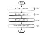
図4は本発明の一実施形態による表示装置100の検査方法を概略的に示したフローチャートである。 FIG. 4 is a flowchart schematically showing an inspection method for the
図1、図2、図3A、図3B、図3C、及び図4を参照すれば、本発明の一実施形態による表示装置100の検査方法は、表示パネル110及び表示パネル上に配置される保護フィルム120を含む表示装置100に第1入射角θ11を有するように第1入射光L11を提供する段階(S110)、表示装置100に第1入射角θ11より大きい第2入射角θ21を有するように第2入射光L21を提供する段階(S120)、表示装置100に第2入射角θ21より大きい第3入射角θ31を有するように第3入射光L31を提供する段階(S130)、及び第1入射光L11が表示装置100で第1反射角θ12に反射されて提供される第1反射光L12、第2入射光L21が表示装置100で第2反射角θ22に反射されて提供される第2反射光L22、及び第3入射光L31が表示装置100で第3反射角θ32に反射されて提供される第3反射光L32のうち、少なくとも1つの光を受信して、表示装置100の欠陥を検出する段階(S200)を含む。 Referring to FIGS. 1, 2, 3A, 3B, 3C, and 4, the method for inspecting the
第1入射光L11を提供する段階(S110)、第2入射光L21を提供する段階(S120)、及び第3入射光L31を提供する段階(S130)は順次的になされてもよく、ランダムな順序になされてもよい。 The step of providing the first incident light L11 (S110), the step of providing the second incident light L21 (S120), and the step of providing the third incident light L31 (S130) may be sequentially performed. May be made in order.
第1入射光L11を提供する段階(S110)は第1照明ユニット210によって遂行される。第1照明ユニット210は表示装置100に第1入射角θ11を有するように第1入射光L11を提供する。第1入射光L11は表示装置の基準軸AXと第1入射角θ11をなす。表示装置の基準軸AXは表示パネル110の厚さ方向と平行である。第1入射角θ11はこれに限定されないが、例えば、0°乃至5°である。 The step (S110) of providing the first incident light L11 is performed by the
表示装置100に第1入射光L11が提供されれば、第1入射光L11は表示装置100で第1反射角θ12に反射されて、第1反射光L12を発生させる。第1反射光L12は欠陥検出部300に提供される。 When the first incident light L11 is provided to the
第1反射光L12は保護フィルム120の上面で反射される第1保護反射光L12_1及び保護フィルム120を透過して、表示パネル110の上面で反射される第1表示反射光L12_2を含む。 The first reflected light L12 includes the first protective reflected light L12_1 reflected by the upper surface of the
表示装置100に第1入射光L11が提供されれば、表示パネル110に存在する欠陥111、保護フィルム120に存在する欠陥121、表示パネル110に付着された異物質112、保護フィルム120に付着された異物質122等によって、第1散乱光L13が発生する。第1散乱光L13は欠陥検出部300に提供される。 If the first incident light L11 is provided to the
第1散乱光L13は保護フィルム120に存在する欠陥121によって散乱される第1保護散乱光L13_3、表示パネル110に存在する欠陥111によって散乱される第1表示散乱光L13_4、保護フィルム120に付着されたほこりやごみ等の異物質122によって散乱される第1保護異物質散乱光L13_1、及び表示パネル110に付着されたほこりやごみ等の異物質112によって散乱される第1表示異物質散乱光L13_2を含む。 The first scattered light L13 is attached to the first protective scattered light L13_3 scattered by the
第1入射光L11を提供する段階(S110)は、光を提供する第1光源211を配置する段階及び第1光源211及び表示装置100の間に第1偏光板212を配置する段階を含む。第1光源211は表示装置100に光を提供する。第1偏光板212は第1光源211及び表示装置100の間に配置される。第1偏光板212は第1光源211から提供された光を偏光する。第1偏光板212は通常的に使用するものであれば、特別に限定しないが、直線偏光板、円偏光板、又は楕円偏光板であってもよい。 The step (S110) of providing the first incident light L11 includes the step of disposing the first
第1入射光L11を提供する段階(S110)は、第1光源211及び表示装置100の間にバンドパスフィルターBPFを配置する段階をさらに含む。図2では、バンドパスフィルターBPFが第1光源211及び第1偏光板212の間に配置されることを例として図示したが、これに限定されなく、バンドパスフィルターBPFは第1偏光板212及び表示装置100の間に配置されてもよい。 Providing the first incident light L11 (S110) further includes disposing a band pass filter BPF between the first
第2入射光L21を提供する段階(S120)は第2照明ユニット220によって遂行される。第2照明ユニット220は表示装置100に第2入射光L21を提供する。第2入射光L21は表示装置の基準軸AXと第2入射角θ21をなす。表示装置の基準軸AXは表示パネル110の厚さ方向と平行である。第2入射角θ21は第1入射角θ11より大きい。第2入射角θ21はこれに限定されないが、例えば、10°乃至20°である。第2照明ユニット220は第2入射光L21が表示装置100に提供される時、第1入射角θ11と異なる第2入射角θ21を有するように配置されて、第1照明ユニット210で検査し難い欠陥を追加的に検査することができる。 The providing of the second incident light L21 (S120) is performed by the
表示装置100に第2入射光L21が提供されれば、第2入射光L21は表示装置100で第2反射角θ22に反射されて、第2反射光L22を発生させる。第2反射光L22は欠陥検出部300に提供される。 When the second incident light L21 is provided to the
第2反射光L22は保護フィルム120の上面で反射される第2保護反射光L22_1及び保護フィルム120を透過して、表示パネル110の上面で反射される第2表示反射光L22_2を含む。 The second reflected light L22 includes the second protective reflected light L22_1 reflected by the upper surface of the
表示装置100に第2入射光L21が提供されれば、表示パネル110に存在する欠陥111、保護フィルム120に存在する欠陥121、表示パネル110に付着された異物質112、保護フィルム120に付着された異物質122等によって第2散乱光L23が発生する。第2散乱光L23は欠陥検出部300に提供される。 If the second incident light L21 is provided to the
第2散乱光L23は保護フィルム120に存在する欠陥121によって散乱される第2保護散乱光L23_3、表示パネル110に存在する欠陥111によって散乱される第2表示散乱光L23_4、保護フィルム120に付着されたほこりやごみ等の異物質122によって散乱される第2保護異物質散乱光L23_1、及び表示パネル110に付着されたほこりやごみ等の異物質112によって散乱される第2表示異物質散乱光L23_2を含む。 The second scattered light L23 is attached to the second protective scattered light L23_3 scattered by the
第2入射光L21を提供する段階(S120)は光を提供する第2光源221を配置する段階及び第2光源221及び表示装置100の間に第2偏光板222を配置する段階を含む。第2光源221は表示装置100に光を提供する。第2偏光板222は第2光源221及び表示装置100の間に配置される。第2偏光板222は第2光源221から提供された光を偏光する。第2偏光板222は第1偏光板212と同一の成分を偏光する。第2偏光板222は通常的に使用するものであれば、特別に限定しないが、直線偏光板、円偏光板、又は楕円偏光板であってもよい。 The step of providing the second incident light L <b> 21 (S <b> 120) includes a step of disposing the second
第3入射光L31を提供する段階S130は第3照明ユニット230によって遂行される。第3照明ユニット230は表示装置100に第3入射光L31を提供する。第3入射光L31は表示装置の基準軸AXと第3入射角θ31をなす。表示装置の基準軸AXは表示パネル110の厚さ方向と平行である。第3入射角θ31は第1入射角θ11及び第2入射角θ21の各々より大きい。 The step S130 of providing the third incident light L31 is performed by the
表示装置100に第3入射光L31が提供されれば、第3入射光L31は表示装置100で第3反射角θ32に反射されて、第3反射光L32を発生させる。第3反射光L32は欠陥検出部300に提供される。 When the third incident light L31 is provided to the
第3反射光L32は保護フィルム120の上面で反射される第3保護反射光L32_1及び保護フィルム120を透過して、表示パネル110の上面で反射される第3表示反射光L32_2を含む。 The third reflected light L32 includes the third protective reflected light L32_1 reflected by the upper surface of the
表示装置100に第3入射光L31が提供されれば、表示パネル110に存在する欠陥111、保護フィルム120に存在する欠陥121、表示パネル110に付着された異物質112、保護フィルム120に付着された異物質122等によって第3散乱光L33が発生する。第3散乱光L33は欠陥検出部300に提供される。 If the third incident light L31 is provided to the
第3散乱光L33は保護フィルム120に存在する欠陥121によって散乱される第3保護散乱光L33_3、表示パネル110に存在する欠陥111によって散乱される第3表示散乱光L33_4、保護フィルム120に付着されたほこりやごみ等の異物質122によって散乱される第3保護異物質散乱光L33_1、及び表示パネル110に付着されたほこりやごみ等の異物質112によって散乱される第3表示異物質散乱光L33_2を含む。第3照明ユニット230は第3保護異物質散乱光L33_1の量が極大化されるように配置される。 The third scattered light L33 is attached to the third protective scattered light L33_3 scattered by the
第3入射光L31を提供する段階S130は光を提供する第3光源231を配置する段階及び第3光源231及び表示装置100の間に第3偏光板232を配置する段階を含む。第3光源231は表示装置100に光を提供する。第3偏光板232は第3光源231及び表示装置100の間に配置される。第3偏光板232は第3光源231から提供された光を偏光する。第3偏光板232は第1偏光板212及び第2偏光板222の各々と異なる成分を偏光する。第3偏光板232は通常的に使用するものであれば、特別に限定しないが、直線偏光板、円偏光板、又は楕円偏光板であってもよい。 The step S130 of providing the third incident light L31 includes the step of disposing the third
表示装置100の欠陥を検出する段階(S200)は、第1反射光L12、第2反射光L22及び第3反射光L32のうち、少なくとも1つの光を受信して表示装置100を撮影して表示装置のイメージPSを提供する段階、及び表示装置のイメージPSを受けて表示装置100の欠陥を検出する段階を含む。 In the step of detecting a defect of the display device 100 (S200), at least one of the first reflected light L12, the second reflected light L22, and the third reflected light L32 is received and the
表示装置のイメージPSを提供する段階は第1反射光L12を受け、表示装置100を撮影して第1表示装置のイメージを提供する段階、第2反射光L22を受け、表示装置100を撮影して第2表示装置のイメージを提供する段階、及び第3反射光L32を受け、表示装置100を撮影して第3表示装置のイメージを提供する段階を含む。 The step of providing the image PS of the display device receives the first reflected light L12, photographs the
表示装置のイメージPSを提供する段階は表示装置100を撮影するカメラ311を配置する段階及びカメラ311及び表示装置100の間に第4偏光板312を配置する段階を含む。 Providing the image PS of the display device includes disposing a
カメラ311は表示装置100を撮影する。カメラ311は通常的に使用するものであれば、特別に限定しないが、CCD(Charge Coupled Device)カメラ及びCMOS(Complementary Metal Oxide Semiconductor)カメラのうち、少なくとも1つを含む。 The
第4偏光板312はカメラ311及び表示装置100の間に配置される。第4偏光板312は第1反射光L12、第2反射光L22、第3反射光L32、第1散乱光L13、第2散乱光L23、及び第3散乱光L33のうち、少なくとも1つの光を偏光させる。第4偏光板312は第1偏光板212及び第2偏光板222の各々と互いに異なる成分を偏光する。第4偏光板312は第3偏光板232と同一の成分を偏光する。第4偏光板312は通常的に使用するものであれば、特別に限定しないが、直線偏光板、円偏光板、又は楕円偏光板であってもよい。 The fourth
表示装置100の欠陥を検出する段階は制御部320によって遂行される。制御部320は表示パネル110の欠陥111、保護フィルム120の欠陥121、及び表示パネル110に付着された異物質112及び保護フィルム120に付着された異物質122を区別することができる。 The step of detecting a defect in the
制御部320は第1表示装置のイメージ、第2表示装置のイメージ及び第3表示装置のイメージを比較して、表示パネル110に存在する欠陥111、保護フィルム120に存在する欠陥121、表示パネル110の上面及び保護フィルム120の上面の各々に付着されたほこりやごみ等の異物質を区別することができる。 The
例えば、第1表示装置のイメージには表示パネル110の欠陥111、保護フィルム120の欠陥121、表示パネル110に付着された異物質112、及び保護フィルム120に付着された異物質122が存在する領域が歪曲されて表示される。第2表示装置のイメージには表示パネル110の欠陥111、保護フィルム120の欠陥121、表示パネル110に付着された異物質112及び保護フィルム120に付着された異物質122が存在する領域が歪曲されて表示される。第3表示装置のイメージには表示パネル110の欠陥111、保護フィルム120の欠陥121及び表示パネル110に付着された異物質112が存在する領域が歪曲されて表示される。先に言及したように、第3照明ユニット230は第3保護散乱光L33_3の量が最大化されるように配置されるので、第3表示装置のイメージでは保護フィルム120に付着された異物質122が存在する領域は明るく表示される。 For example, in the image of the first display device, a region where a
したがって、第1表示装置のイメージ及び第2表示装置のイメージの各々を第3表示装置のイメージと比べると、保護フィルム120に付着された異物質122が存在する領域を検出することができる。 Therefore, when each of the image of the first display device and the image of the second display device is compared with the image of the third display device, it is possible to detect a region where the
第1表示装置のイメージ、第2表示装置のイメージの各々では保護フィルム120に付着された異物質122が存在する領域を除外すれば、保護フィルム120の欠陥121が存在する領域が最も明るく表示され、表示パネル110の欠陥111が存在する領域が最も暗く表示される。表示パネル110の欠陥111が存在する領域の場合、表示パネル110の欠陥111で散乱された散乱光が表示パネル110と保護フィルム120とを透過し、撮影ユニット310に提供されるので、光損失量が多く、相対的に暗く表示される。 In each of the image of the first display device and the image of the second display device, if the region where the
本発明の一実施形態による表示装置の検査方法は第1入射光を提供する段階、第2入射光を提供する段階、及び第3入射光を提供する段階を含み、表示パネルに保護フィルムが付着されていても、表示パネルの欠陥、保護フィルムの欠陥及び表示パネルに付着された異物質、及び保護フィルムに付着された異物質を区別することができる。 A method for inspecting a display device according to an embodiment of the present invention includes providing a first incident light, providing a second incident light, and providing a third incident light, and a protective film is attached to the display panel. Even if it is made, the defect of a display panel, the defect of a protective film, the foreign substance adhering to a display panel, and the foreign substance adhering to a protective film can be distinguished.
以上、添付された図面を参照して本発明の実施形態を説明したが、本発明が属する技術分野で通常の知識を有する者は、本発明がその技術的思想や必須的な特徴を変形せず、他の具体的な形態に実施できることを理解できる。したがって、以上で記述した実施形態は、すべての面で例示的なことであり、限定的なことではないと理解しなければならない。 The embodiments of the present invention have been described above with reference to the accompanying drawings. However, those skilled in the art to which the present invention pertains have ordinary skill in the art to change the technical idea and essential features thereof. However, it can be understood that the present invention can be implemented in other specific forms. Accordingly, it should be understood that the embodiments described above are illustrative in all aspects and not limiting.
10 表示装置の検査装置
100 表示装置
110 表示パネル
120 保護フィルム
210 第1照明ユニット
211 第1光源
212 第1偏光板
220 第2照明ユニット
221 第2光源
222 第2偏光板
230 第3照明ユニット
231 第3光源
232 第3偏光板
300 欠陥検出部
310 撮影ユニット
311 カメラ
312 第4偏光板
320 制御部
230 第3照明ユニットDESCRIPTION OF
Claims (10)
Translated fromJapanese前記表示装置に前記第1入射角より大きい第2入射角を有するように第2入射光を提供する第2照明ユニットと、
前記表示装置に前記第2入射角より大きい第3入射角を有するように第3入射光を提供する第3照明ユニットと、を備え、
前記第1入射光が前記表示装置で第1反射角に反射されて提供される第1反射光、前記第2入射光が前記表示装置で第2反射角に反射されて提供される第2反射光、及び前記第3入射光が前記表示装置で第3反射角に反射されて提供される第3反射光のうち、少なくとも1つの光を受信して、前記表示装置の欠陥を検出する欠陥検出部を含む、表示装置の検査装置。A first illumination unit that provides first incident light to a display device including a display panel and a protective film disposed on the display panel so as to have a first incident angle;
A second illumination unit for providing second incident light to the display device so as to have a second incident angle larger than the first incident angle;
A third illumination unit for providing a third incident light to the display device so as to have a third incident angle larger than the second incident angle;
The first incident light is provided by being reflected at the first reflection angle by the display device, and the second reflection is provided by the second incident light being reflected by the display device at the second reflection angle. Defect detection for detecting a defect of the display device by receiving at least one of the light and the third reflected light provided by the display device reflecting the third incident light at a third reflection angle. Inspecting device for display device including a section.
前記表示装置に光を提供する第1光源と、
前記第1光源及び前記表示装置の間に配置される第1偏光板と、を含み、
前記第1偏光板は、
直線偏光板、円偏光板、又は楕円偏光板である請求項1に記載の表示装置の検査装置。The first lighting unit includes:
A first light source for providing light to the display device;
A first polarizing plate disposed between the first light source and the display device,
The first polarizing plate is
The inspection apparatus for a display device according to claim 1, which is a linearly polarizing plate, a circularly polarizing plate, or an elliptically polarizing plate.
前記第1光源及び前記表示装置の間に配置されるバンドパスフィルターをさらに含む請求項2に記載の表示装置の検査装置。The first lighting unit includes:
The display device inspection apparatus according to claim 2, further comprising a band pass filter disposed between the first light source and the display device.
前記表示装置に光を提供する第2光源と、
前記第2光源及び前記表示装置の間に配置される第2偏光板と、を含み、
前記第2偏光板は、
直線偏光板、円偏光板、又は楕円偏光板である請求項1に記載の表示装置の検査装置。The second lighting unit includes:
A second light source for providing light to the display device;
A second polarizing plate disposed between the second light source and the display device,
The second polarizing plate is
The inspection apparatus for a display device according to claim 1, which is a linearly polarizing plate, a circularly polarizing plate, or an elliptically polarizing plate.
前記表示装置に光を提供する第3光源と、
前記第3光源及び前記表示装置の間に配置される第3偏光板と、を含み、
前記第3偏光板は、
直線偏光板、円偏光板、又は楕円偏光板である請求項1に記載の表示装置の検査装置。The third lighting unit includes:
A third light source for providing light to the display device;
A third polarizing plate disposed between the third light source and the display device,
The third polarizing plate is
The inspection apparatus for a display device according to claim 1, which is a linearly polarizing plate, a circularly polarizing plate, or an elliptically polarizing plate.
前記第2照明ユニットは、第2偏光板を含み、
前記第3照明ユニットは、第3偏光板を含み、
前記第1偏光板及び前記第2偏光板は、互いに同一の成分を偏光し、
前記第1偏光板及び前記第3偏光板は、互いに異なる成分を偏光する請求項1に記載の表示装置の検査装置。The first lighting unit includes a first polarizing plate,
The second lighting unit includes a second polarizing plate,
The third lighting unit includes a third polarizing plate,
The first polarizing plate and the second polarizing plate polarize the same component,
The inspection apparatus for a display device according to claim 1, wherein the first polarizing plate and the third polarizing plate polarize different components.
前記第1反射光、前記第2反射光、及び前記第3反射光のうち、少なくとも1つの光を受信して、前記表示装置を撮影する撮影ユニットと、
前記撮影ユニットから表示装置のイメージを受けて前記表示装置の欠陥を検出する制御部と、を含む請求項1に記載の表示装置の検査装置。The defect detection unit
An imaging unit that receives at least one of the first reflected light, the second reflected light, and the third reflected light and images the display device;
The display device inspection apparatus according to claim 1, further comprising: a control unit that receives an image of the display device from the photographing unit and detects a defect of the display device.
前記表示装置を撮影するカメラと、
前記カメラ及び前記表示装置の間に配置される第4偏光板と、を含む請求項7に記載の表示装置の検査装置。The photographing unit is
A camera for photographing the display device;
The display device inspection apparatus according to claim 7, further comprising a fourth polarizing plate disposed between the camera and the display device.
前記第2照明ユニットは、第2偏光板を含み、
前記第3照明ユニットは、第3偏光板を含み、
前記撮影ユニットは、第4偏光板を含み、
前記第1偏光板及び前記第2偏光板は、互いに同一の成分を偏光し、
前記第3偏光板及び前記第4偏光板は、互いに同一の成分を偏光し、
前記第1偏光板及び前記第3偏光板は、互いに異なる成分を偏光する請求項7に記載の表示装置の検査装置。The first lighting unit includes a first polarizing plate,
The second lighting unit includes a second polarizing plate,
The third lighting unit includes a third polarizing plate,
The photographing unit includes a fourth polarizing plate,
The first polarizing plate and the second polarizing plate polarize the same component,
The third polarizing plate and the fourth polarizing plate polarize the same component,
The display device inspection apparatus according to claim 7, wherein the first polarizing plate and the third polarizing plate polarize different components.
Applications Claiming Priority (2)
| Application Number | Priority Date | Filing Date | Title |
|---|---|---|---|
| KR10-2014-0192097 | 2014-12-29 | ||
| KR1020140192097AKR102250032B1 (en) | 2014-12-29 | 2014-12-29 | Detecting device of display device and detecting method of display device |
Publications (2)
| Publication Number | Publication Date |
|---|---|
| JP2016126005Atrue JP2016126005A (en) | 2016-07-11 |
| JP6890377B2 JP6890377B2 (en) | 2021-06-18 |
Family
ID=56163805
Family Applications (1)
| Application Number | Title | Priority Date | Filing Date |
|---|---|---|---|
| JP2015241090AActiveJP6890377B2 (en) | 2014-12-29 | 2015-12-10 | Display device inspection device and display device inspection method |
Country Status (5)
| Country | Link |
|---|---|
| US (1) | US9835565B2 (en) |
| JP (1) | JP6890377B2 (en) |
| KR (1) | KR102250032B1 (en) |
| CN (1) | CN105738380B (en) |
| TW (1) | TW201623944A (en) |
Cited By (4)
| Publication number | Priority date | Publication date | Assignee | Title |
|---|---|---|---|---|
| WO2022044952A1 (en)* | 2020-08-28 | 2022-03-03 | 住友化学株式会社 | Inspection method |
| WO2022044951A1 (en)* | 2020-08-28 | 2022-03-03 | 住友化学株式会社 | Inspection method |
| WO2022044988A1 (en)* | 2020-08-28 | 2022-03-03 | 住友化学株式会社 | Inspection method |
| JP2023110350A (en)* | 2022-01-28 | 2023-08-09 | 住友化学株式会社 | Inspection method |
Families Citing this family (16)
| Publication number | Priority date | Publication date | Assignee | Title |
|---|---|---|---|---|
| JP6604805B2 (en)* | 2015-09-30 | 2019-11-13 | 日東電工株式会社 | Polarizer inspection method and polarizing plate manufacturing method |
| IT201600095896A1 (en)* | 2016-09-23 | 2018-03-23 | Paola Ferrari | Automatic control machine. |
| JP7075853B2 (en)* | 2017-09-13 | 2022-05-26 | 住友化学株式会社 | Defect inspection device, defect inspection method, manufacturing method of circular polarizing plate or elliptical polarizing plate, manufacturing method of retardation plate |
| KR102233918B1 (en)* | 2018-06-22 | 2021-03-30 | 주식회사 엘지화학 | System for inspecting foreign matter of display unit |
| CN108982520A (en)* | 2018-08-03 | 2018-12-11 | 汕头超声显示器(二厂)有限公司 | A kind of detection method and device of film bottom visible defects |
| US20210299879A1 (en)* | 2018-10-27 | 2021-09-30 | Gilbert Pinter | Machine vision systems, illumination sources for use in machine vision systems, and components for use in the illumination sources |
| CN109387524A (en)* | 2018-12-12 | 2019-02-26 | 长安大学 | Thread defect detection method and device based on linearly polarized photon |
| DE102019112317A1 (en)* | 2019-05-10 | 2020-11-12 | Deutsches Zentrum für Luft- und Raumfahrt e.V. | Method and device for the detection of surface defects |
| CN110220915B (en)* | 2019-06-21 | 2025-01-24 | 银河水滴科技(北京)有限公司 | Glass inspection machine |
| CN110261408B (en)* | 2019-07-30 | 2021-11-23 | 云谷(固安)科技有限公司 | Display module defect detection device and method |
| CN110398849B (en)* | 2019-07-31 | 2024-03-22 | 北京兆维电子(集团)有限责任公司 | Optical detection system for liquid crystal display screen |
| CN110658207A (en)* | 2019-09-30 | 2020-01-07 | 武汉精立电子技术有限公司 | Detection method and device for distinguishing foreign matters inside and outside non-polarizing film |
| TWI791971B (en)* | 2020-04-08 | 2023-02-11 | 財團法人紡織產業綜合研究所 | Cloth inspection machine |
| CN111505849A (en)* | 2020-06-16 | 2020-08-07 | 湖南大学 | A kind of LCD display screen finished product defect detection imaging device and method |
| KR102765451B1 (en)* | 2022-11-21 | 2025-02-11 | (주)펨트론 | Inspection apparatus for reel tape |
| KR102762562B1 (en)* | 2022-12-08 | 2025-02-04 | 주식회사 앤비젼 | Apparatus detecting fine particle and automatic optical inspector including the same, and method detecting fine particle |
Citations (7)
| Publication number | Priority date | Publication date | Assignee | Title |
|---|---|---|---|---|
| JPS6273141A (en)* | 1985-09-27 | 1987-04-03 | Hitachi Ltd | Defect detection method and device for transparent samples |
| JPH05334420A (en)* | 1992-06-04 | 1993-12-17 | Matsushita Electric Ind Co Ltd | Image signal processor for judging parts arrangement status |
| JP2002162360A (en)* | 2000-11-22 | 2002-06-07 | Seiko Epson Corp | Method and apparatus for evaluating liquid crystal panel |
| JP2005043371A (en)* | 2003-07-23 | 2005-02-17 | Kla-Tencor Technologies Corp | Method and apparatus for determining surface layer thickness using continuous multi-wavelength surface scanning |
| US20110058038A1 (en)* | 2009-09-04 | 2011-03-10 | Lockheed Martin Corporation | Single camera color polarimetric imaging |
| JP2012063245A (en)* | 2010-09-16 | 2012-03-29 | Nitto Denko Corp | Test device and method for manufacturing wiring circuit board |
| JP2014142339A (en)* | 2012-12-31 | 2014-08-07 | Djtech Co Ltd | Inspection device |
Family Cites Families (16)
| Publication number | Priority date | Publication date | Assignee | Title |
|---|---|---|---|---|
| US4889998A (en)* | 1987-01-29 | 1989-12-26 | Nikon Corporation | Apparatus with four light detectors for checking surface of mask with pellicle |
| JP2512878B2 (en)* | 1987-01-29 | 1996-07-03 | 株式会社ニコン | Foreign matter inspection device |
| JP4003371B2 (en) | 2000-04-03 | 2007-11-07 | 凸版印刷株式会社 | Circuit board inspection apparatus and circuit board inspection method |
| KR100437024B1 (en)* | 2001-10-18 | 2004-06-23 | 엘지전자 주식회사 | The inspection method of thin film and the same apparatus |
| JP2004170495A (en)* | 2002-11-18 | 2004-06-17 | Micronics Japan Co Ltd | Display substrate inspection method and apparatus |
| TW200540939A (en) | 2004-04-22 | 2005-12-16 | Olympus Corp | Defect inspection device and substrate manufacturing system using the same |
| JP4736629B2 (en) | 2005-08-26 | 2011-07-27 | 株式会社ニコン | Surface defect inspection equipment |
| JP2008058207A (en) | 2006-09-01 | 2008-03-13 | Sumika Chemical Analysis Service Ltd | Cartridge and pretreatment device for cadmium analysis comprising the cartridge |
| JP2008058270A (en) | 2006-09-04 | 2008-03-13 | Mitsubishi Electric Corp | Polycrystalline silicon substrate inspection method, solar cell inspection method, and infrared inspection apparatus |
| KR20100021051A (en) | 2008-08-14 | 2010-02-24 | 엘지전자 주식회사 | Apparatus and method for inspecting liquid crytal display panel |
| NL2003263A (en)* | 2008-08-20 | 2010-03-10 | Asml Holding Nv | Particle detection on an object surface. |
| KR101379817B1 (en) | 2009-07-07 | 2014-04-01 | 엘지디스플레이 주식회사 | Apparatus for inspecting back light assembly and apparatus for inspecting display device |
| JP2011226939A (en) | 2010-04-21 | 2011-11-10 | Hitachi High-Technologies Corp | Method and device for inspecting substrate |
| JP2012119512A (en)* | 2010-12-01 | 2012-06-21 | Hitachi High-Technologies Corp | Substrate quality evaluation method and apparatus therefor |
| JP5594254B2 (en) | 2011-08-09 | 2014-09-24 | 三菱電機株式会社 | Silicon substrate inspection apparatus and inspection method |
| US9787916B2 (en)* | 2014-10-28 | 2017-10-10 | The Boeing Company | Active real-time characterization system |
- 2014
- 2014-12-29KRKR1020140192097Apatent/KR102250032B1/enactiveActive
- 2015
- 2015-06-22USUS14/746,427patent/US9835565B2/enactiveActive
- 2015-12-10JPJP2015241090Apatent/JP6890377B2/enactiveActive
- 2015-12-14TWTW104141905Apatent/TW201623944A/enunknown
- 2015-12-25CNCN201510997280.2Apatent/CN105738380B/enactiveActive
Patent Citations (7)
| Publication number | Priority date | Publication date | Assignee | Title |
|---|---|---|---|---|
| JPS6273141A (en)* | 1985-09-27 | 1987-04-03 | Hitachi Ltd | Defect detection method and device for transparent samples |
| JPH05334420A (en)* | 1992-06-04 | 1993-12-17 | Matsushita Electric Ind Co Ltd | Image signal processor for judging parts arrangement status |
| JP2002162360A (en)* | 2000-11-22 | 2002-06-07 | Seiko Epson Corp | Method and apparatus for evaluating liquid crystal panel |
| JP2005043371A (en)* | 2003-07-23 | 2005-02-17 | Kla-Tencor Technologies Corp | Method and apparatus for determining surface layer thickness using continuous multi-wavelength surface scanning |
| US20110058038A1 (en)* | 2009-09-04 | 2011-03-10 | Lockheed Martin Corporation | Single camera color polarimetric imaging |
| JP2012063245A (en)* | 2010-09-16 | 2012-03-29 | Nitto Denko Corp | Test device and method for manufacturing wiring circuit board |
| JP2014142339A (en)* | 2012-12-31 | 2014-08-07 | Djtech Co Ltd | Inspection device |
Cited By (13)
| Publication number | Priority date | Publication date | Assignee | Title |
|---|---|---|---|---|
| JP7413211B2 (en) | 2020-08-28 | 2024-01-15 | 住友化学株式会社 | Inspection method |
| WO2022044951A1 (en)* | 2020-08-28 | 2022-03-03 | 住友化学株式会社 | Inspection method |
| WO2022044988A1 (en)* | 2020-08-28 | 2022-03-03 | 住友化学株式会社 | Inspection method |
| JP2022039687A (en)* | 2020-08-28 | 2022-03-10 | 住友化学株式会社 | Inspection method |
| JP2022039690A (en)* | 2020-08-28 | 2022-03-10 | 住友化学株式会社 | Inspection method |
| JP2022039692A (en)* | 2020-08-28 | 2022-03-10 | 住友化学株式会社 | Inspection method |
| JP7413210B2 (en) | 2020-08-28 | 2024-01-15 | 住友化学株式会社 | Inspection method |
| JP7413209B2 (en) | 2020-08-28 | 2024-01-15 | 住友化学株式会社 | Inspection method |
| WO2022044952A1 (en)* | 2020-08-28 | 2022-03-03 | 住友化学株式会社 | Inspection method |
| TWI884307B (en)* | 2020-08-28 | 2025-05-21 | 日商住友化學股份有限公司 | Inspection method |
| TWI884308B (en)* | 2020-08-28 | 2025-05-21 | 日商住友化學股份有限公司 | Inspection method |
| JP2023110350A (en)* | 2022-01-28 | 2023-08-09 | 住友化学株式会社 | Inspection method |
| JP7723619B2 (en) | 2022-01-28 | 2025-08-14 | 住友化学株式会社 | Inspection method |
Also Published As
| Publication number | Publication date |
|---|---|
| JP6890377B2 (en) | 2021-06-18 |
| CN105738380B (en) | 2021-04-06 |
| CN105738380A (en) | 2016-07-06 |
| KR20160082787A (en) | 2016-07-11 |
| US9835565B2 (en) | 2017-12-05 |
| TW201623944A (en) | 2016-07-01 |
| KR102250032B1 (en) | 2021-05-12 |
| US20160187262A1 (en) | 2016-06-30 |
Similar Documents
| Publication | Publication Date | Title |
|---|---|---|
| JP6890377B2 (en) | Display device inspection device and display device inspection method | |
| US8803968B2 (en) | Apparatus for detecting particles in flat glass and detecting method using same | |
| TWI782086B (en) | Defect inspection apparatus, defect inspection method, manufacturing method of circular polarizing plate or oval polarizing plate, and manufacturing method of retardation plate | |
| JP2015017981A (en) | Polarizing plate inspection method | |
| TW201632868A (en) | Substrate examination device | |
| JP2005049158A (en) | Foreign film inspection method for transparent film | |
| JP2011226957A (en) | Polarizing plate defect inspection method and defect inspection apparatus | |
| CN107615051A (en) | Defect inspection method of light transmissive film, method of manufacturing linear polarizer film, and method of manufacturing polarizing plate | |
| KR101678169B1 (en) | Upper Surface Foreign Matter Detection Device of Ultra-Thin Transparent Substrate | |
| TW201610420A (en) | Substrate inspection apparatus | |
| CN1501073A (en) | Inspection method and device of display panel | |
| KR102632190B1 (en) | Imaging apparatus for obtaining image of polarizing film, inspection apparatus, and inspection method | |
| JP2015137927A (en) | imaging device and inspection system | |
| WO2013117100A1 (en) | Method for determining position of touch point on touch panel, and touch panel | |
| US11906442B2 (en) | Foreign material inspection system of display unit | |
| JP2012185091A (en) | Device and method for inspecting silicon substrate | |
| JP2007322316A (en) | Polarization-selective imaging device | |
| KR20160005445A (en) | Apparatus of inspecting defect of polarizing plate and method of inspecting the same | |
| JP2013210245A (en) | Film inspection system, and film inspection method | |
| JP2014095775A (en) | Device for inspecting lamination position of polarizing film | |
| CN108174098A (en) | A dust detection device and method | |
| KR100834730B1 (en) | Defect Inspection System of Liquid Crystal Display Panel Using Vision Sensor System | |
| JP2008241469A (en) | Defect inspection apparatus | |
| JP2018009810A (en) | Defect inspection system and film manufacturing device | |
| JP2014178215A (en) | Inspection equipment |
Legal Events
| Date | Code | Title | Description |
|---|---|---|---|
| RD02 | Notification of acceptance of power of attorney | Free format text:JAPANESE INTERMEDIATE CODE: A7422 Effective date:20180810 | |
| RD04 | Notification of resignation of power of attorney | Free format text:JAPANESE INTERMEDIATE CODE: A7424 Effective date:20181102 | |
| A621 | Written request for application examination | Free format text:JAPANESE INTERMEDIATE CODE: A621 Effective date:20181129 | |
| A977 | Report on retrieval | Free format text:JAPANESE INTERMEDIATE CODE: A971007 Effective date:20190717 | |
| A131 | Notification of reasons for refusal | Free format text:JAPANESE INTERMEDIATE CODE: A131 Effective date:20190723 | |
| A521 | Request for written amendment filed | Free format text:JAPANESE INTERMEDIATE CODE: A523 Effective date:20191016 | |
| A131 | Notification of reasons for refusal | Free format text:JAPANESE INTERMEDIATE CODE: A131 Effective date:20200331 | |
| A521 | Request for written amendment filed | Free format text:JAPANESE INTERMEDIATE CODE: A523 Effective date:20200629 | |
| A131 | Notification of reasons for refusal | Free format text:JAPANESE INTERMEDIATE CODE: A131 Effective date:20201013 | |
| A521 | Request for written amendment filed | Free format text:JAPANESE INTERMEDIATE CODE: A523 Effective date:20210108 | |
| TRDD | Decision of grant or rejection written | ||
| A01 | Written decision to grant a patent or to grant a registration (utility model) | Free format text:JAPANESE INTERMEDIATE CODE: A01 Effective date:20210510 | |
| A61 | First payment of annual fees (during grant procedure) | Free format text:JAPANESE INTERMEDIATE CODE: A61 Effective date:20210525 | |
| R150 | Certificate of patent or registration of utility model | Ref document number:6890377 Country of ref document:JP Free format text:JAPANESE INTERMEDIATE CODE: R150 | |
| R250 | Receipt of annual fees | Free format text:JAPANESE INTERMEDIATE CODE: R250 |