JP2016122654A - Inductive plasma source with metal showerhead using B field concentrator - Google Patents
Inductive plasma source with metal showerhead using B field concentratorDownload PDFInfo
- Publication number
- JP2016122654A JP2016122654AJP2016002248AJP2016002248AJP2016122654AJP 2016122654 AJP2016122654 AJP 2016122654AJP 2016002248 AJP2016002248 AJP 2016002248AJP 2016002248 AJP2016002248 AJP 2016002248AJP 2016122654 AJP2016122654 AJP 2016122654A
- Authority
- JP
- Japan
- Prior art keywords
- conductive
- lid assembly
- disposed
- induction coil
- coil
- Prior art date
- Legal status (The legal status is an assumption and is not a legal conclusion. Google has not performed a legal analysis and makes no representation as to the accuracy of the status listed.)
- Pending
Links
Images

Classifications
- H—ELECTRICITY
- H01—ELECTRIC ELEMENTS
- H01J—ELECTRIC DISCHARGE TUBES OR DISCHARGE LAMPS
- H01J37/00—Discharge tubes with provision for introducing objects or material to be exposed to the discharge, e.g. for the purpose of examination or processing thereof
- H01J37/32—Gas-filled discharge tubes
- H01J37/32009—Arrangements for generation of plasma specially adapted for examination or treatment of objects, e.g. plasma sources
- H01J37/32082—Radio frequency generated discharge
- H01J37/321—Radio frequency generated discharge the radio frequency energy being inductively coupled to the plasma
- H01J37/3211—Antennas, e.g. particular shapes of coils
- C—CHEMISTRY; METALLURGY
- C23—COATING METALLIC MATERIAL; COATING MATERIAL WITH METALLIC MATERIAL; CHEMICAL SURFACE TREATMENT; DIFFUSION TREATMENT OF METALLIC MATERIAL; COATING BY VACUUM EVAPORATION, BY SPUTTERING, BY ION IMPLANTATION OR BY CHEMICAL VAPOUR DEPOSITION, IN GENERAL; INHIBITING CORROSION OF METALLIC MATERIAL OR INCRUSTATION IN GENERAL
- C23C—COATING METALLIC MATERIAL; COATING MATERIAL WITH METALLIC MATERIAL; SURFACE TREATMENT OF METALLIC MATERIAL BY DIFFUSION INTO THE SURFACE, BY CHEMICAL CONVERSION OR SUBSTITUTION; COATING BY VACUUM EVAPORATION, BY SPUTTERING, BY ION IMPLANTATION OR BY CHEMICAL VAPOUR DEPOSITION, IN GENERAL
- C23C16/00—Chemical coating by decomposition of gaseous compounds, without leaving reaction products of surface material in the coating, i.e. chemical vapour deposition [CVD] processes
- C23C16/44—Chemical coating by decomposition of gaseous compounds, without leaving reaction products of surface material in the coating, i.e. chemical vapour deposition [CVD] processes characterised by the method of coating
- C23C16/455—Chemical coating by decomposition of gaseous compounds, without leaving reaction products of surface material in the coating, i.e. chemical vapour deposition [CVD] processes characterised by the method of coating characterised by the method used for introducing gases into reaction chamber or for modifying gas flows in reaction chamber
- C23C16/45563—Gas nozzles
- C23C16/45565—Shower nozzles
- C—CHEMISTRY; METALLURGY
- C23—COATING METALLIC MATERIAL; COATING MATERIAL WITH METALLIC MATERIAL; CHEMICAL SURFACE TREATMENT; DIFFUSION TREATMENT OF METALLIC MATERIAL; COATING BY VACUUM EVAPORATION, BY SPUTTERING, BY ION IMPLANTATION OR BY CHEMICAL VAPOUR DEPOSITION, IN GENERAL; INHIBITING CORROSION OF METALLIC MATERIAL OR INCRUSTATION IN GENERAL
- C23C—COATING METALLIC MATERIAL; COATING MATERIAL WITH METALLIC MATERIAL; SURFACE TREATMENT OF METALLIC MATERIAL BY DIFFUSION INTO THE SURFACE, BY CHEMICAL CONVERSION OR SUBSTITUTION; COATING BY VACUUM EVAPORATION, BY SPUTTERING, BY ION IMPLANTATION OR BY CHEMICAL VAPOUR DEPOSITION, IN GENERAL
- C23C16/00—Chemical coating by decomposition of gaseous compounds, without leaving reaction products of surface material in the coating, i.e. chemical vapour deposition [CVD] processes
- C23C16/44—Chemical coating by decomposition of gaseous compounds, without leaving reaction products of surface material in the coating, i.e. chemical vapour deposition [CVD] processes characterised by the method of coating
- C23C16/50—Chemical coating by decomposition of gaseous compounds, without leaving reaction products of surface material in the coating, i.e. chemical vapour deposition [CVD] processes characterised by the method of coating using electric discharges
- C23C16/505—Chemical coating by decomposition of gaseous compounds, without leaving reaction products of surface material in the coating, i.e. chemical vapour deposition [CVD] processes characterised by the method of coating using electric discharges using radio frequency discharges
- C23C16/509—Chemical coating by decomposition of gaseous compounds, without leaving reaction products of surface material in the coating, i.e. chemical vapour deposition [CVD] processes characterised by the method of coating using electric discharges using radio frequency discharges using internal electrodes
- C23C16/5096—Flat-bed apparatus
- H—ELECTRICITY
- H01—ELECTRIC ELEMENTS
- H01J—ELECTRIC DISCHARGE TUBES OR DISCHARGE LAMPS
- H01J37/00—Discharge tubes with provision for introducing objects or material to be exposed to the discharge, e.g. for the purpose of examination or processing thereof
- H01J37/32—Gas-filled discharge tubes
- H01J37/32431—Constructional details of the reactor
- H01J37/3244—Gas supply means
- H—ELECTRICITY
- H01—ELECTRIC ELEMENTS
- H01J—ELECTRIC DISCHARGE TUBES OR DISCHARGE LAMPS
- H01J37/00—Discharge tubes with provision for introducing objects or material to be exposed to the discharge, e.g. for the purpose of examination or processing thereof
- H01J37/32—Gas-filled discharge tubes
- H01J37/32431—Constructional details of the reactor
- H01J37/32532—Electrodes
- H01J37/32541—Shape
- H—ELECTRICITY
- H01—ELECTRIC ELEMENTS
- H01J—ELECTRIC DISCHARGE TUBES OR DISCHARGE LAMPS
- H01J2237/00—Discharge tubes exposing object to beam, e.g. for analysis treatment, etching, imaging
- H01J2237/32—Processing objects by plasma generation
- H01J2237/33—Processing objects by plasma generation characterised by the type of processing
Landscapes
- Chemical & Material Sciences (AREA)
- Engineering & Computer Science (AREA)
- Physics & Mathematics (AREA)
- Plasma & Fusion (AREA)
- Analytical Chemistry (AREA)
- Chemical Kinetics & Catalysis (AREA)
- General Chemical & Material Sciences (AREA)
- Materials Engineering (AREA)
- Mechanical Engineering (AREA)
- Metallurgy (AREA)
- Organic Chemistry (AREA)
- Plasma Technology (AREA)
- Chemical Vapour Deposition (AREA)
- Drying Of Semiconductors (AREA)
- Cleaning In General (AREA)
Abstract
Translated fromJapaneseDescription
Translated fromJapanese本明細書に記載の実施形態は、一般に、半導体デバイスを製造することに関する。より詳細には、本明細書に記載の実施形態は、基板のプラズマ処理のための方法および装置に関する。 Embodiments described herein generally relate to manufacturing semiconductor devices. More particularly, the embodiments described herein relate to a method and apparatus for plasma processing of a substrate.
プラズマ処理は、通常、集積回路、フラットパネルディスプレイ、磁気媒体、および他のデバイスを製造するための多くの半導体製造プロセスに使用される。プラズマまたはイオン化ガスは、処理チャンバの内側で、チャンバ内の低圧のガスに電磁場を印加することにより生成され、次いで、被加工物に適用されて、堆積、エッチング、または注入などのプロセスを達成する。プラズマを、チャンバの外側で生成し、次いで、そのような処置を必要とするプロセスのために、プラズマ中のラジカルのイオンに対する比を増加させるように圧力をかけてチャンバの中に導くこともできる。 Plasma processing is typically used in many semiconductor manufacturing processes to manufacture integrated circuits, flat panel displays, magnetic media, and other devices. A plasma or ionized gas is generated inside the processing chamber by applying an electromagnetic field to the low pressure gas in the chamber and then applied to the workpiece to achieve a process such as deposition, etching, or implantation. . A plasma can be generated outside the chamber and then directed into the chamber under pressure to increase the ratio of radicals to ions in the plasma for processes that require such treatment. .
プラズマは、電場によって、磁場によって、または電磁場によって生成することができる。電場によって生成されるプラズマは、ガスによって占められる空間内に電場を生成するために、普通は、離間した電極を使用する。電場はガスをイオン化し、結果として生じるイオンおよび電子は、電場の影響下で一方の電極または他方の電極に向かって移動する。電場は、被加工物上に当たるイオンに非常に高いエネルギーを付与する場合があり、このことによって、被加工物から材料をスパッタし、被加工物に損傷を与え、チャンバ内に潜在的な汚染粒子を作る場合がある。加えて、そのようなプラズマをともなう高電位は、不要な放電および寄生電流を作る可能性がある。 The plasma can be generated by an electric field, by a magnetic field, or by an electromagnetic field. The plasma generated by the electric field typically uses spaced electrodes to generate an electric field in the space occupied by the gas. The electric field ionizes the gas and the resulting ions and electrons move toward one or the other electrode under the influence of the electric field. The electric field can impart very high energy to the ions impinging on the workpiece, thereby sputtering material from the workpiece, damaging the workpiece, and potentially contaminating particles in the chamber. May make. In addition, high potentials with such plasmas can create unwanted discharges and parasitic currents.
誘導結合プラズマは、容量結合プラズマのいくつかの効果を回避するために、多くの状況で使用される。誘導コイルが、処理チャンバのプラズマ生成領域に隣接して配設される。誘導コイルは、チャンバ内に磁場を投射し、チャンバ内部のガスをイオン化する。誘導コイルは、しばしばチャンバの外側に配置され、誘電性の窓を介してチャンバ内に磁場を投射する。誘導コイルは、しばしば高周波電磁エネルギーにより駆動され、高周波電磁エネルギーには、誘導コイルに印加される電圧より速く大きくなる電力損失がある。したがって、プラズマ源とチャンバ内側のプラズマが強く結合することによって、電力損失を減少させる。プラズマ均一性の制御も、プラズマ源とプラズマの間の強い結合によって改善される。 Inductively coupled plasmas are used in many situations to avoid some of the effects of capacitively coupled plasmas. An induction coil is disposed adjacent to the plasma generation region of the processing chamber. The induction coil projects a magnetic field into the chamber and ionizes the gas inside the chamber. Induction coils are often placed outside the chamber and project a magnetic field into the chamber through a dielectric window. Induction coils are often driven by high frequency electromagnetic energy, which has a power loss that increases faster than the voltage applied to the induction coil. Therefore, the power loss is reduced by the strong coupling between the plasma source and the plasma inside the chamber. Control of plasma uniformity is also improved by the strong coupling between the plasma source and the plasma.
様々な半導体産業におけるデバイスの形状寸法が減少しつづけるので、一般的にはプロセス均一性、具体的にはプラズマ均一性が、デバイスを信頼性高く製造することに、ますます有益になる。したがって、誘導性プラズマ処理装置および方法には、引き続き必要性がある。 As device geometries in various semiconductor industries continue to decrease, in general process uniformity, specifically plasma uniformity, becomes increasingly beneficial for reliable device manufacturing. Accordingly, there remains a need for inductive plasma processing apparatus and methods.
本明細書に記載の実施形態は、プラズマチャンバ用のリッドアセンブリを提供し、リッドアセンブリは、第1の導電リングと入れ子になった第1の環状誘導コイルを有する。 Embodiments described herein provide a lid assembly for a plasma chamber, the lid assembly having a first annular induction coil nested with a first conductive ring.
他の実施形態は、半導体基板用の処理チャンバを提供し、処理チャンバは、内部領域を画定するチャンバ本体、内部領域内に配設される基板支持体、および基板支持体に面し内部領域内に配設されるリッドアセンブリを有し、リッドアセンブリは、ガス分配器ならびに基板支持体に面する第1の導電表面、基板支持体から離れる向きである第2の導電表面、および第1の表面および第2の表面の間の導電性プラズマ源に配設される複数の導電コイルを備えるプラズマ源を有する。 Other embodiments provide a processing chamber for a semiconductor substrate, the processing chamber defining a chamber body defining an interior region, a substrate support disposed within the interior region, and facing the substrate support within the interior region. A lid assembly disposed on the substrate, the lid assembly having a first conductive surface facing the gas distributor and the substrate support, a second conductive surface facing away from the substrate support, and a first surface And a plasma source comprising a plurality of conductive coils disposed in the conductive plasma source between the second surface.
他の実施形態は、基板を処理チャンバ内の基板支持体上に配設するステップと、基板支持体に面するプラズマ源をもうけるステップであって、プラズマ源が、電極中に配設される複数の導電ループを備え、プラズマ源と基板支持体の間に処理領域を画定するステップと、ガス混合物を処理領域に提供するステップと、電極を接地するステップと、導電ループに電力を印加することによりガス混合物からプラズマを形成するステップによって、基板を処理する方法を提供する。 Another embodiment includes disposing a substrate on a substrate support in a processing chamber and providing a plasma source facing the substrate support, wherein the plasma source is disposed in an electrode. A conductive region, defining a processing region between the plasma source and the substrate support, providing a gas mixture to the processing region, grounding the electrode, and applying power to the conductive loop A method is provided for processing a substrate by forming a plasma from a gas mixture.
本発明の上記の特徴を詳細に理解することが可能なやり方を、上で簡単に要約された本発明のより具体的な説明が実施形態を参照することによってわかることができるように、その一部が添付の図面に示されている。しかし、他の同様に有効な実施形態を本発明が容認することができるので、添付の図面は、本発明の単に典型的な実施形態を示しており、したがって本発明の範囲を限定すると考えるべきでないことに留意されたい。 The manner in which the above features of the invention can be understood in detail will be understood by reference to the embodiments so that a more specific description of the invention briefly summarized above can be seen by reference to the embodiments. The parts are shown in the accompanying drawings. However, since the present invention may accept other equally effective embodiments, the accompanying drawings show merely exemplary embodiments of the invention and are therefore to be considered as limiting the scope of the invention. Note that it is not.
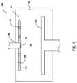
図1は、一実施形態にしたがう、処理チャンバ100の概略断面の線図である。処理チャンバ100は、チャンバ本体102、基板支持体104、および基板支持体104に面するガス分配器106を備え、チャンバ本体102、基板支持体104、およびガス分配器106は、協働的に処理領域118を画定する。ガス分配器106は、シャワーヘッド108およびシャワーヘッド108を囲むプラズマ源110を備える。プラズマ源110は、導電スペーサ114および導電スペーサ114の内側に配設される導電コイル112を備える。導電スペーサ114内に配設される、1つまたは複数の導電コイル112があって良い。導電スペーサ114は、導電コイル112を収容するチャンネルまたはコンジットを備えるディスク様の部材であって良い。交互に、導電スペーサ114は、導電コイル112を分離し、導電コイル112と入れ子になる複数のリングであって良い。導電コイル112のそれぞれは、絶縁材料で裏打ちされるチャンネルまたは凹部116内に収容される。チャンネルまたは凹部116の絶縁材料は、電流が導電コイル112から導電スペーサ114の中に伝わることを防止する。導電コイル112は、処理領域118内に磁場を作り、磁場は、処理領域118内に配設される処理ガスをイオン化してプラズマを形成する。いくつかの実施形態において、導電コイル112は、図2に関連して下でさらに記載されるように、取外し可能な絶縁部材を特徴として有するコイルアセンブリであって良い。 FIG. 1 is a schematic cross-sectional diagram of a
導電スペーサ114は、基板支持体104に面する、大きな表面積の接地電極をもうける。大きな接地電極によって、より低い電力レベルを使用して、基板支持体において、より高い電圧を生成することが可能になる。導電スペーサ114内に導電コイル112を配設することによって、同様に、プラズマ源を処理領域118のプラズマ生成区域に近づけて、プラズマとの結合効率を改善する。加えて、導電スペーサ114の大きな接地表面積によって、チャンバ内のプラズマシース電圧を減少させ、このことがチャンバ壁およびチャンバリッド構成要素のスパッタリングを減少させ、基板支持体上に配設される被加工物の汚染を減少させる。複数の導電コイル112を使用することによって、同様に、処理領域118内のプラズマプロファイルを調整するため、コイルに異なる電力レベルを使用する可能性をもたらす。 The
図2は、別の実施形態にしたがう、リッドアセンブリ200の概略断面の線図である。図1のガス分配器106と同様に、リッドアセンブリ200はシャワーヘッド202およびプラズマ源204を備える。ガスコンジット206は、ガス源(図示せず)をシャワーヘッド202に接続し、ガス源をシャワーヘッド202内の開口208を介して処理チャンバと流体連結の状態にする。 FIG. 2 is a schematic cross-sectional diagram of a
プラズマ源204は、導電性ガス分配部材214間に形成されるチャンネル212内に配設される導電コイル210を備える。いくつかの実施形態において、ガス分配部材214は、金属または金属合金であって良く、所望であれば、誘電体材料で、またはイットリアなどの化学的耐性のあるまたはプラズマ耐性のある材料でコーティングすることができる。導電コイル210は、1つより多い導電コイル210が存在して良いが、同様に金属、金属合金、または金属でコーティングされた誘電体もしくは異なる導電率を有する金属を特徴として有する金属複合物などの、導電性複合物であって良い。導電コイル210のための材料の選択は、一般的に、所望の熱伝導率および電気伝導率に依存する。より低い電気伝導率を有する材料は、一般的にコストがより低いが、より低い伝導率の材料から作られた導電コイルは、不要な熱を生成する場合があり、動作させるために過剰な電力が必要な場合がある。銅および銀などの、より導電性の高い材料は、導電コイル用にうまく使用することができる。アルミニウム、亜鉛、またはニッケルなどの導電性が低く、より低コストの材料を、合金または層の構成要素として含むことができる。 The
水などの冷却液体または窒素などの冷却ガスであって良い熱制御媒体用のコンジットを備える導電コイル210を形成することにより、熱を放散することができる。導電コイル210は、いくつかの実施形態において、環状またはトロイダル状の管であって良い。管壁の厚さは、必要な熱伝導率および電気伝導率に基づいて規定することができる。冷却は、例えば約500Wを超える大電力が、導電コイル210に印加されるときに有用な場合がある。一実施形態において、導電コイルは、銅の層および銀の層を備えるトロイダル管である。 Heat can be dissipated by forming a
チャンネル212は、一般的に、セラミックまたはプラスチック、例えばテフロン(登録商標)であって良い、絶縁部材216で裏打ちされる。絶縁部材216は、電流を導電コイル210に閉じ込める。絶縁材料は、チャンネル212内に嵌入する挿入物であって良く、または他の実施形態では、チャンネル212の内部表面に付着されるライナであって良い。図2の実施形態は、2つの絶縁部材216を特徴として有し、絶縁部材216のそれぞれは、それぞれのチャンネルの内側に嵌合する環状部材であり、絶縁部材216のうちの1つは、図2の実施形態内の第1のチャンネルである、最内チャンネル212の内側に嵌合し、他の絶縁部材216は、図2の実施形態内の第2のチャンネルである、最外チャンネル212の内側に嵌合する。チャンネル212のそれぞれは、チャンネル212の中に配設される導電コイル210を有する。図2の実施形態において、各導電コイルは、2つの導電ループ218を備える。1対の導電ループ218が、それぞれの絶縁部材216により形成される凹部の内側に載る。 The
2つの導電ループ218は、それぞれの導電ループ218を囲むように働く、それぞれのアイソレータ220によって、お互いが電気的に隔離される。図2の実施形態において、各アイソレータ220は、導電ループ218が嵌入する凹部224を有する環状の誘電体部材である。アイソレータ220の凹部224とアイソレータ220が嵌入するチャンネル212は、一般的に、反対方向に向く。したがって、各導電ループは、アイソレータ220により3つの側を、絶縁部材216により1つの側を囲まれる。アイソレータ220は、任意の都合の良い断面形状を有して良いことに留意されたい。例えば、代替実施形態において、凹部224が丸みのある断面形状を有するように、アイソレータ220は、丸みのある管状の導電ループ218の輪郭にしたがうために丸みをつけることができる。別の実施形態において、各アイソレータ220および/または各凹部224の断面プロファイルは、斜角をつけたコーナを有する矩形であって良い。さらに他の実施形態において、導電ループ218は、ループを隔離するコーティングを用いて形成することができる。アイソレータ220は、セラミック、ガラス、またはプラスチックなどの任意の絶縁材料であって良い。図2の実施形態において、各アイソレータ220は、単一の導電ループ218を覆う単一の部片として示されるが、代替実施形態において、アイソレータは、2つの隣接する導電ループ218を覆うように形成する一方で、2つの隣接する導電ループ218の間に壁を配設することができる。 The two
フィールド集中装置222が、各導電コイル210の周りに配設され、各導電コイル210により生成される磁場を増幅する。図2の実施形態において、集中装置222は、1対の導電ループ218および導電ループ218それぞれのアイソレータ220の周りに配設されるが、他の実施形態において、各ループ218をフィールド集中装置222と対にすることができ、または2つより多いループをフィールド集中装置222と結合することができる。フィールド集中装置222は、各導電コイル210により生成される磁場を、処理チャンバのプラズマ生成区域に向けて集束させ、プラズマ生成区域から離れて投射する磁気エネルギーを最小化する。各フィールド集中装置222は、一般的に、フェライトまたは低保持力材料などの他の磁気感受性材料または磁化可能材料を含む。導電コイル210を熱制御することよって、フィールド集中装置222の温度変動を最小化し、導電コイル210により生成される磁場を制御するために、フィールド集中装置222の磁気特性を維持する。 A
誘電コイル210は、絶縁部材216と入れ子になり、協働的にチャンネル212を画定する、ガス分配部材214の中に挿置される。導電部材226も、誘導コイル210およびガス分配部材214と挿置される。一実施形態において、導電部材226は、金属、金属合金、または金属混合物を含むリングであり、導電部材226のそれぞれを支持部材228に取り付けることができる。絶縁部材216は、導電部材226とガス分配部材214の間に嵌合し、導電部材214および226と実質的に共平面構成のチャンネル212をもうけ、そのため、誘導コイル210は、導電部材214および226と実質的に共平面である。 The
支持部材228も一般的に導電性である。いくつかの実施形態において、支持部材228は、金属ブロックである。支持部材228は凹部230を有し、凹部230は導電部材226とともに取込み空間232を画定し、取込み空間232の中に各絶縁部材216の肩の部分234が取り込まれて、絶縁部材216をリッドアセンブリ200の中に固定する。導電部材214および226によって、プラズマの極近傍に大きな接地表面をもたらすことが可能になり、より低い電力レベルおよびより低い熱入力で、基板支持体上で使用されるより高いバイアス電圧を可能にする(図1)。図2のリッドアセンブリ構成は、同様に、誘導コイル210のプラズマ源エネルギーを処理領域内のガスの極近傍にもたらして、より低い電力レベルでより高いプラズマ密度を生じさせる。誘導コイル210などの複数の誘導コイルを使用することによっても、各個々のコイルに印加される電力レベルを調節することによりチャンバ内で生成されるプラズマプロファイルの調整を可能にする。
支持部材228は、プロセスガスを導電性ガス分配部材214にもたらす、1つまたは複数のコンジット236を備える。加えて、いくつかの実施形態において、導電性ガス分配部材214はコンジット(図示せず)を備え、均一なガス分配のため、ガス分配部材214の周囲の周りにコンジット236からガスを分散させることができる。導電性ガス分配部材214を誘導コイル210で挿置することにより、装置200は、プラズマ源とシャワーヘッドの両方として使用することができる。ガス流は、装置の面にわたって均一に分配され、RF電力は、様々な開口を出るプロセスガスに近接結合される。
熱制御は、場合によって支持部材228内に熱制御コンジット240を含むことにより、向上させることができる。支持部材228内に熱制御コンジットを配置することによって、フィールド集中装置222の熱制御を向上させることができ、フィールド集中装置222は、他の場合には、ループ218を通って循環する任意の熱制御流体から少なくとも部分的にアイソレータ220により絶縁される。フィールド集中装置222の近傍の熱制御は、フィールド集中装置222の電磁特性を維持するのに有利な場合がある。また場合によっては、クッション238がフィールド集中装置222と支持部材228の間に配設されて、フィールド集中装置222への任意の損傷を回避することができる。フィールド集中装置222は、支持部材228の金属表面と直接接触することにより容易に損傷を受ける可能性がある。クッション238は、GrafTech Internationalの子会社であり、オハイオ州Lakewoodの、Natural Graphite Operationsにより製造され、テキサス州Deer ParkのLeader Global Technologiesにより流通される、可撓性黒鉛シーリング材料である、Grafoil(登録商標)などの、熱的に伝導性の材料であって良い。 Thermal control can be improved by optionally including a
一般に、リッドアセンブリ200は、任意の寸法の基板を処理するための、任意の都合の良い形状またはサイズを有することができる。リッドアセンブリ200は、円形、矩形または任意の多角形形状であって良い。リッドアセンブリ200は、任意の種類の半導体チップを作るための半導体ウエハを処理するために適合されるサイズおよび形状であって良く、またはリッドアセンブリ200は、大画面ディスプレイまたは太陽パネルなどの半導体パネルを処理するために適合されるサイズおよび形状であって良い。LED基板または磁気媒体基板などの他のタイプの基板も、本明細書に記載のリッドアセンブリを使用して処理することができる。いくつかの実施形態において、導電コイル(または複数のコイル)210は、同心の円形形状で、同心の非円形(矩形、多角形、正方形、または不規則)形状で、または牛耕式またはジグザグパターンなどの非同心の形状で配設することができる。別の非同心の実施形態において、導電コイル(または複数のコイル)210は、螺旋パターンで配設することができる。 In general, the
いくつかの実施形態において、リッドアセンブリは、いくつかの差異を備えるが、図2のリッドアセンブリ200に類似することができる。一実施形態において、リッドアセンブリは、基板支持体に向いた曲がった表面を有することができ、曲がったとは、凸状または凹状の意味である。一態様において、プラズマ源全体が曲がっていて良い(すなわち、基板支持体に向いたプラズマ源の表面および基板支持体から離れる向きの表面が両方とも凸状または凹状である)。別の態様において、基板支持体に向いたリッドアセンブリの表面のみが曲がっていて良い。一実施形態において、特に大面積リッドアセンブリ用に、複数のシャワーヘッドがもうけられて良い。一実施形態において、支持部材228を通して1つまたは複数のコンジットをもうけることによって、導電部材226を通してガスを注入することができる。他の実施形態において、複数のディスクリート回路ではなく、単一の電気回路を備える導電コイルをもうけることができる。例えば、一実施形態において、導電コイルを、相補的な導電部材と入れ子になる、または相補的な導電部材内に配設される、平坦な、円形のまたは矩形の螺旋形状に配置し、そのため、導電部材および導電コイルが実質的に平坦なプラズマ源を形成することができる。そのような螺旋形状を、zにずらし、そのため、プラズマ源が平坦でなく、凸状または凹状という意味で、z次元を有することもできる。 In some embodiments, the lid assembly may be similar to the
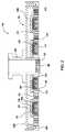
図3は、別の実施形態にしたがう、リッドアセンブリ300の分解図である。リッドアセンブリ300は、図2のリッドアセンブリ200と大部分に関して同様であり、同一の特徴は、同じ識別ラベルで標示される。リッドアセンブリ300は、リッドアセンブリ300が設置されるチャンバのプロセス領域にガスを送達するためのコンジット206を備える。リッドアセンブリ300は、第1のRFコイル302および第1のRFコイルと同様の第2のRFコイル304をさらに備え、第1のRFコイル302は、分解された形で示される。第1のRFコイル302は、絶縁チャンネル308内に配設される複数の導体306を備える。図3の実施形態において、導体306は、円形かつ同心であるが、代替実施形態において、導体306は、本明細書に記載するように、任意の都合の良い構成に配設することができる。導体306のそれぞれは、導体306に電力を供給するための接点310を有する。本明細書の他の場所に記載のように、導体306は、電力に加えて冷却剤を運ぶように構成される導電管であって良い。したがって、接点310も、導体306に冷却剤を提供するために使用することができる。 FIG. 3 is an exploded view of a
導体306は、一般的に金属または他の電気的に導電性の材料である。金属は、単一の金属、合金、混合物、または金属の別の組合せであって良い。導体306は、いくつかの実施形態において、セラミックまたはポリマーなどの非導電材料でコーティングすることもできる。一実施形態において、導体306は、銀メッキされた銅管である。使用される金属は、一般的に、特定の実施形態に必要な電気特性および熱特性に依存する。大電力用途では、より高い電気伝導率は、一般的により低いサーマルバジェットをもたらすことになり、そのためより導電性の材料が有利な場合がある。複数のRFコイルが使用されるとき、コイルのそれぞれが異なる組成物を有する場合があることに留意されたい。例えば、銀メッキされた銅管は、銀メッキの異なる厚さまたは異なる管壁厚を有し、管の間で、異なる導電率を実現することができる。他の実施形態において、各RFコイルは、単に1つの導体、または2つより多い導体を有する場合がある。
絶縁体312が導体306の上に配設され、そのため、導体306は、絶縁性材料によって囲まれる。このことが、第1のRFコイル302と第2のRFコイル304の間に挿置される導電リング314および316に電力が流れることを防止する。絶縁体312は、図3の上面斜視図では見えない壁を備える。壁は、2つの導体306間に延在して、所与のRFコイル302または304内の導体306間の電気的なクロストークを防止する。したがって、各導体306は、絶縁材料によって囲まれる。導体306に電力が提供されると、導体306によって磁場が生成される。フィールド集中装置318は、部分的に導体306の周りに配設され、効率改善のために磁場を処理ゾーンの方向に集束させ、かつ磁場を処理ゾーンの方向に向ける。 An
絶縁体312は、各接点310用に通路320をさらに備える。通路320は、フィールド集中装置318内の開口を通過して、電力と結合される接点310用の経路を実現すると同時に、接点310とフィールド集中装置318の間が電気的に接触することを防止する。接点は、フィールド集中装置318を通って突出し、そこで接点がRF源と結合することができる。
図2の実施形態と同様に、任意の数のRFコイルを、リッドアセンブリ300内に配設することができる。導電リング314および316の中に開口とともにコンジットをもうけてプロセスガスを処理ゾーン内に放出することによって、コンジット206に加えて、またはコンジット206のかわりに導電リング314および316を通して、プロセスガスを提供することもできる。リッドアセンブリ300は、本明細書に記載の実施形態のいずれかにしたがって、湾曲を有して形成することもできる。 Similar to the embodiment of FIG. 2, any number of RF coils can be disposed in the
本明細書に開示の実施形態は、プロセスチャンバ内の基板支持体上の基板を処理する方法も提供する。プラズマ源を、基板支持体に面する位置にもうけ、基板を処理するプラズマを形成することができる。方法は、電極に配設される複数の導電ループを有するプラズマ源をもうけるステップと、チャンバに処理ガスを提供するステップと、電極を接地するステップと、導電ループに電力を印加することにより処理ガスからプラズマを形成するステップとを含む。導電ループは、コーティングすること、ラッピングすること、またはループを電気的な絶縁材料内に据えることにより電極から電気的に絶縁することができ、電気的な絶縁材料は、電極内に形成されるチャンネル、導電ループに塗布されるコーティング、または電極内に形成されるチャンネルの内側に配設されるライナなどの容器であって良い。RF電力がループに印加され、独立に制御されて、プロセスチャンバ内でプラズマ密度を成形することができる。導電ループは、所望であれば、管状導電ループを通して冷却流体などの熱制御媒体を循環させることにより、熱的に制御することができる。 The embodiments disclosed herein also provide a method of processing a substrate on a substrate support in a process chamber. A plasma source can be provided at a position facing the substrate support to form a plasma for processing the substrate. The method includes providing a plasma source having a plurality of conductive loops disposed on the electrodes, providing a process gas to the chamber, grounding the electrodes, and applying a power to the conductive loops. Forming a plasma from. The conductive loop can be electrically isolated from the electrode by coating, wrapping, or placing the loop in an electrically insulating material, and the electrically insulating material is a channel formed in the electrode. It may be a coating applied to the conductive loop, or a container such as a liner disposed inside a channel formed in the electrode. RF power can be applied to the loop and independently controlled to shape the plasma density within the process chamber. The conductive loop can be thermally controlled, if desired, by circulating a thermal control medium such as a cooling fluid through the tubular conductive loop.
導電ループは、いくつかの実施形態において、電極と実質的に共平面であって良い。他の実施形態において、電極は、電極内に配設される導電ループを有する、非平面であって良い。さらに他の実施形態において、導電ループを、部分的には電極の中に配設し、部分的には電極の外側に配設して、電極の外側に配設される導電ループの任意の部分を、絶縁材料の中に含む、または封入することができる。 The conductive loop may be substantially coplanar with the electrode in some embodiments. In other embodiments, the electrode may be non-planar with a conductive loop disposed within the electrode. In still other embodiments, the conductive loop is disposed partially within the electrode, partially disposed outside the electrode, and any portion of the conductive loop disposed outside the electrode. Can be contained or encapsulated in an insulating material.
プラズマは、処理チャンバのプラズマ領域内側の場を集中させるために配設されるフィールド集中装置をもうけることによって、さらに強化することができる。例えば、フィールド集中装置は、導電ループがフィールド集中装置と基板支持体の間にあるように、一般的に基板支持体と対向して配設することができる。そのような配置によって、チャンバの外側に磁場の向きの線が展開することを防止し、プラズマ源のエネルギーを処理ガス内に集束させる。 The plasma can be further enhanced by having a field concentrator arranged to concentrate the field inside the plasma region of the processing chamber. For example, the field concentrator can be generally disposed opposite the substrate support such that the conductive loop is between the field concentrator and the substrate support. Such an arrangement prevents the magnetic field lines from spreading out of the chamber and focuses the energy of the plasma source into the process gas.
上記が本発明の実施形態を対象とする一方、本発明の他のさらなる実施形態が、本発明の基本範囲から逸脱することなく考案することができ、本発明の範囲は、以下の特許請求の範囲により決定される。 While the foregoing is directed to embodiments of the present invention, other and further embodiments of the invention may be devised without departing from the basic scope thereof, which is defined by the following claims. Determined by range.
Claims (16)
Translated fromJapaneseを備える、プラズマチャンバ用のリッドアセンブリ。A lid assembly for a plasma chamber comprising a first annular induction coil nested with a first conductive ring.
前記ガス分配器の周りに配設される支持板と、
前記ガス分配器の周りに配設され、前記支持板に連結される導電リングと、
前記導電リングと入れ子になった絶縁チャンネル内に配設される環状誘導コイルと、
前記誘導コイルの周りの前記絶縁チャンネル内に配設されるフィールド集中装置と
を備える、プラズマチャンバ用のリッドアセンブリ。A gas distributor;
A support plate disposed around the gas distributor;
A conductive ring disposed around the gas distributor and coupled to the support plate;
An annular induction coil disposed in an insulating channel nested with the conductive ring;
A lid assembly for a plasma chamber comprising a field concentrator disposed in the insulating channel around the induction coil.
前記内部領域内に配設される基板支持体と、
前記内部領域内に配設され、前記基板支持体に面するリッドアセンブリであって、
ガス分配器、および
前記基板支持体に面する第1の導電表面、前記基板支持体から離れる向きである第2の導電表面、および前記第1の表面および前記第2の表面の間の導電性プラズマ源に配設される複数の導電コイルを有するプラズマ源を備えるリッドアセンブリと
を備える、半導体基板用処理チャンバ。A chamber body defining an interior region;
A substrate support disposed within the internal region;
A lid assembly disposed in the inner region and facing the substrate support,
A gas distributor; and a first conductive surface facing the substrate support; a second conductive surface facing away from the substrate support; and conductivity between the first surface and the second surface And a lid assembly comprising a plasma source having a plurality of conductive coils disposed in the plasma source.
Applications Claiming Priority (2)
| Application Number | Priority Date | Filing Date | Title |
|---|---|---|---|
| US12/780,531 | 2010-05-14 | ||
| US12/780,531US20110278260A1 (en) | 2010-05-14 | 2010-05-14 | Inductive plasma source with metallic shower head using b-field concentrator |
Related Parent Applications (1)
| Application Number | Title | Priority Date | Filing Date |
|---|---|---|---|
| JP2013511173ADivisionJP2013533575A (en) | 2010-05-14 | 2011-04-25 | Inductive plasma source with metal showerhead using B field concentrator |
Publications (1)
| Publication Number | Publication Date |
|---|---|
| JP2016122654Atrue JP2016122654A (en) | 2016-07-07 |
Family
ID=44910845
Family Applications (2)
| Application Number | Title | Priority Date | Filing Date |
|---|---|---|---|
| JP2013511173APendingJP2013533575A (en) | 2010-05-14 | 2011-04-25 | Inductive plasma source with metal showerhead using B field concentrator |
| JP2016002248APendingJP2016122654A (en) | 2010-05-14 | 2016-01-08 | Inductive plasma source with metal showerhead using B field concentrator |
Family Applications Before (1)
| Application Number | Title | Priority Date | Filing Date |
|---|---|---|---|
| JP2013511173APendingJP2013533575A (en) | 2010-05-14 | 2011-04-25 | Inductive plasma source with metal showerhead using B field concentrator |
Country Status (6)
| Country | Link |
|---|---|
| US (3) | US20110278260A1 (en) |
| JP (2) | JP2013533575A (en) |
| KR (1) | KR101826843B1 (en) |
| CN (1) | CN102893705B (en) |
| TW (1) | TWI520169B (en) |
| WO (1) | WO2011142957A2 (en) |
Cited By (1)
| Publication number | Priority date | Publication date | Assignee | Title |
|---|---|---|---|---|
| US10629415B2 (en) | 2017-03-28 | 2020-04-21 | Asm Ip Holding B.V. | Substrate processing apparatus and method for processing substrate |
Families Citing this family (105)
| Publication number | Priority date | Publication date | Assignee | Title |
|---|---|---|---|---|
| US20110278260A1 (en)* | 2010-05-14 | 2011-11-17 | Applied Materials, Inc. | Inductive plasma source with metallic shower head using b-field concentrator |
| US9449793B2 (en)* | 2010-08-06 | 2016-09-20 | Lam Research Corporation | Systems, methods and apparatus for choked flow element extraction |
| US10658161B2 (en)* | 2010-10-15 | 2020-05-19 | Applied Materials, Inc. | Method and apparatus for reducing particle defects in plasma etch chambers |
| JP5745812B2 (en)* | 2010-10-27 | 2015-07-08 | 東京エレクトロン株式会社 | Plasma processing equipment |
| US10283321B2 (en) | 2011-01-18 | 2019-05-07 | Applied Materials, Inc. | Semiconductor processing system and methods using capacitively coupled plasma |
| US9064815B2 (en) | 2011-03-14 | 2015-06-23 | Applied Materials, Inc. | Methods for etch of metal and metal-oxide films |
| US10271416B2 (en)* | 2011-10-28 | 2019-04-23 | Applied Materials, Inc. | High efficiency triple-coil inductively coupled plasma source with phase control |
| TWI596644B (en)* | 2012-03-22 | 2017-08-21 | 藍姆研究公司 | Fluid distribution member assembly for plasma processing apparatus |
| US9267739B2 (en) | 2012-07-18 | 2016-02-23 | Applied Materials, Inc. | Pedestal with multi-zone temperature control and multiple purge capabilities |
| TW201405627A (en)* | 2012-07-20 | 2014-02-01 | Applied Materials Inc | Symmetrical inductively coupled plasma source with coaxial RF feed and coaxial shielding |
| US9373517B2 (en) | 2012-08-02 | 2016-06-21 | Applied Materials, Inc. | Semiconductor processing with DC assisted RF power for improved control |
| US9132436B2 (en) | 2012-09-21 | 2015-09-15 | Applied Materials, Inc. | Chemical control features in wafer process equipment |
| US10256079B2 (en) | 2013-02-08 | 2019-04-09 | Applied Materials, Inc. | Semiconductor processing systems having multiple plasma configurations |
| US9362130B2 (en) | 2013-03-01 | 2016-06-07 | Applied Materials, Inc. | Enhanced etching processes using remote plasma sources |
| US9309598B2 (en) | 2014-05-28 | 2016-04-12 | Applied Materials, Inc. | Oxide and metal removal |
| US9966240B2 (en) | 2014-10-14 | 2018-05-08 | Applied Materials, Inc. | Systems and methods for internal surface conditioning assessment in plasma processing equipment |
| US9355922B2 (en) | 2014-10-14 | 2016-05-31 | Applied Materials, Inc. | Systems and methods for internal surface conditioning in plasma processing equipment |
| US11637002B2 (en) | 2014-11-26 | 2023-04-25 | Applied Materials, Inc. | Methods and systems to enhance process uniformity |
| US10573496B2 (en) | 2014-12-09 | 2020-02-25 | Applied Materials, Inc. | Direct outlet toroidal plasma source |
| US10224210B2 (en)* | 2014-12-09 | 2019-03-05 | Applied Materials, Inc. | Plasma processing system with direct outlet toroidal plasma source |
| US11257693B2 (en) | 2015-01-09 | 2022-02-22 | Applied Materials, Inc. | Methods and systems to improve pedestal temperature control |
| US10249479B2 (en)* | 2015-01-30 | 2019-04-02 | Applied Materials, Inc. | Magnet configurations for radial uniformity tuning of ICP plasmas |
| US9728437B2 (en) | 2015-02-03 | 2017-08-08 | Applied Materials, Inc. | High temperature chuck for plasma processing systems |
| US20160225652A1 (en) | 2015-02-03 | 2016-08-04 | Applied Materials, Inc. | Low temperature chuck for plasma processing systems |
| US9881805B2 (en) | 2015-03-02 | 2018-01-30 | Applied Materials, Inc. | Silicon selective removal |
| US9741593B2 (en) | 2015-08-06 | 2017-08-22 | Applied Materials, Inc. | Thermal management systems and methods for wafer processing systems |
| US9691645B2 (en) | 2015-08-06 | 2017-06-27 | Applied Materials, Inc. | Bolted wafer chuck thermal management systems and methods for wafer processing systems |
| US9349605B1 (en) | 2015-08-07 | 2016-05-24 | Applied Materials, Inc. | Oxide etch selectivity systems and methods |
| US10504700B2 (en) | 2015-08-27 | 2019-12-10 | Applied Materials, Inc. | Plasma etching systems and methods with secondary plasma injection |
| US10522371B2 (en) | 2016-05-19 | 2019-12-31 | Applied Materials, Inc. | Systems and methods for improved semiconductor etching and component protection |
| US10504754B2 (en) | 2016-05-19 | 2019-12-10 | Applied Materials, Inc. | Systems and methods for improved semiconductor etching and component protection |
| US9865484B1 (en) | 2016-06-29 | 2018-01-09 | Applied Materials, Inc. | Selective etch using material modification and RF pulsing |
| US10062575B2 (en) | 2016-09-09 | 2018-08-28 | Applied Materials, Inc. | Poly directional etch by oxidation |
| US10629473B2 (en) | 2016-09-09 | 2020-04-21 | Applied Materials, Inc. | Footing removal for nitride spacer |
| US10546729B2 (en) | 2016-10-04 | 2020-01-28 | Applied Materials, Inc. | Dual-channel showerhead with improved profile |
| US9934942B1 (en)* | 2016-10-04 | 2018-04-03 | Applied Materials, Inc. | Chamber with flow-through source |
| US10062585B2 (en) | 2016-10-04 | 2018-08-28 | Applied Materials, Inc. | Oxygen compatible plasma source |
| US10062579B2 (en) | 2016-10-07 | 2018-08-28 | Applied Materials, Inc. | Selective SiN lateral recess |
| US9947549B1 (en) | 2016-10-10 | 2018-04-17 | Applied Materials, Inc. | Cobalt-containing material removal |
| US10163696B2 (en) | 2016-11-11 | 2018-12-25 | Applied Materials, Inc. | Selective cobalt removal for bottom up gapfill |
| US9768034B1 (en) | 2016-11-11 | 2017-09-19 | Applied Materials, Inc. | Removal methods for high aspect ratio structures |
| US10242908B2 (en) | 2016-11-14 | 2019-03-26 | Applied Materials, Inc. | Airgap formation with damage-free copper |
| US10026621B2 (en) | 2016-11-14 | 2018-07-17 | Applied Materials, Inc. | SiN spacer profile patterning |
| US9953888B1 (en)* | 2016-12-15 | 2018-04-24 | Taiwan Semiconductor Manufacturing Co., Ltd. | Electromagnetic detection device and semiconductor manufacturing system |
| US10566206B2 (en) | 2016-12-27 | 2020-02-18 | Applied Materials, Inc. | Systems and methods for anisotropic material breakthrough |
| US10431429B2 (en) | 2017-02-03 | 2019-10-01 | Applied Materials, Inc. | Systems and methods for radial and azimuthal control of plasma uniformity |
| US10403507B2 (en) | 2017-02-03 | 2019-09-03 | Applied Materials, Inc. | Shaped etch profile with oxidation |
| US10043684B1 (en) | 2017-02-06 | 2018-08-07 | Applied Materials, Inc. | Self-limiting atomic thermal etching systems and methods |
| US10319739B2 (en) | 2017-02-08 | 2019-06-11 | Applied Materials, Inc. | Accommodating imperfectly aligned memory holes |
| US10943834B2 (en) | 2017-03-13 | 2021-03-09 | Applied Materials, Inc. | Replacement contact process |
| US10319649B2 (en) | 2017-04-11 | 2019-06-11 | Applied Materials, Inc. | Optical emission spectroscopy (OES) for remote plasma monitoring |
| CN108882494B (en)* | 2017-05-08 | 2022-06-17 | 北京北方华创微电子装备有限公司 | Plasma device |
| US11276590B2 (en) | 2017-05-17 | 2022-03-15 | Applied Materials, Inc. | Multi-zone semiconductor substrate supports |
| JP7176860B6 (en) | 2017-05-17 | 2022-12-16 | アプライド マテリアルズ インコーポレイテッド | Semiconductor processing chamber to improve precursor flow |
| US11276559B2 (en) | 2017-05-17 | 2022-03-15 | Applied Materials, Inc. | Semiconductor processing chamber for multiple precursor flow |
| US10497579B2 (en) | 2017-05-31 | 2019-12-03 | Applied Materials, Inc. | Water-free etching methods |
| US10049891B1 (en) | 2017-05-31 | 2018-08-14 | Applied Materials, Inc. | Selective in situ cobalt residue removal |
| US10920320B2 (en) | 2017-06-16 | 2021-02-16 | Applied Materials, Inc. | Plasma health determination in semiconductor substrate processing reactors |
| US10541246B2 (en) | 2017-06-26 | 2020-01-21 | Applied Materials, Inc. | 3D flash memory cells which discourage cross-cell electrical tunneling |
| US10727080B2 (en) | 2017-07-07 | 2020-07-28 | Applied Materials, Inc. | Tantalum-containing material removal |
| US10541184B2 (en) | 2017-07-11 | 2020-01-21 | Applied Materials, Inc. | Optical emission spectroscopic techniques for monitoring etching |
| US10354889B2 (en) | 2017-07-17 | 2019-07-16 | Applied Materials, Inc. | Non-halogen etching of silicon-containing materials |
| US10043674B1 (en) | 2017-08-04 | 2018-08-07 | Applied Materials, Inc. | Germanium etching systems and methods |
| US10170336B1 (en) | 2017-08-04 | 2019-01-01 | Applied Materials, Inc. | Methods for anisotropic control of selective silicon removal |
| US10297458B2 (en) | 2017-08-07 | 2019-05-21 | Applied Materials, Inc. | Process window widening using coated parts in plasma etch processes |
| US10128086B1 (en) | 2017-10-24 | 2018-11-13 | Applied Materials, Inc. | Silicon pretreatment for nitride removal |
| US10424487B2 (en) | 2017-10-24 | 2019-09-24 | Applied Materials, Inc. | Atomic layer etching processes |
| US10283324B1 (en) | 2017-10-24 | 2019-05-07 | Applied Materials, Inc. | Oxygen treatment for nitride etching |
| US10256112B1 (en) | 2017-12-08 | 2019-04-09 | Applied Materials, Inc. | Selective tungsten removal |
| US10903054B2 (en) | 2017-12-19 | 2021-01-26 | Applied Materials, Inc. | Multi-zone gas distribution systems and methods |
| US11328909B2 (en) | 2017-12-22 | 2022-05-10 | Applied Materials, Inc. | Chamber conditioning and removal processes |
| US10854426B2 (en) | 2018-01-08 | 2020-12-01 | Applied Materials, Inc. | Metal recess for semiconductor structures |
| KR102560283B1 (en) | 2018-01-24 | 2023-07-26 | 삼성전자주식회사 | Apparatus and method for manufacturing and designing a shower head |
| US10679870B2 (en) | 2018-02-15 | 2020-06-09 | Applied Materials, Inc. | Semiconductor processing chamber multistage mixing apparatus |
| US10964512B2 (en) | 2018-02-15 | 2021-03-30 | Applied Materials, Inc. | Semiconductor processing chamber multistage mixing apparatus and methods |
| TWI766433B (en) | 2018-02-28 | 2022-06-01 | 美商應用材料股份有限公司 | Systems and methods to form airgaps |
| US10593560B2 (en) | 2018-03-01 | 2020-03-17 | Applied Materials, Inc. | Magnetic induction plasma source for semiconductor processes and equipment |
| US10319600B1 (en) | 2018-03-12 | 2019-06-11 | Applied Materials, Inc. | Thermal silicon etch |
| US10497573B2 (en) | 2018-03-13 | 2019-12-03 | Applied Materials, Inc. | Selective atomic layer etching of semiconductor materials |
| US10573527B2 (en) | 2018-04-06 | 2020-02-25 | Applied Materials, Inc. | Gas-phase selective etching systems and methods |
| US10490406B2 (en) | 2018-04-10 | 2019-11-26 | Appled Materials, Inc. | Systems and methods for material breakthrough |
| US10699879B2 (en) | 2018-04-17 | 2020-06-30 | Applied Materials, Inc. | Two piece electrode assembly with gap for plasma control |
| US10886137B2 (en) | 2018-04-30 | 2021-01-05 | Applied Materials, Inc. | Selective nitride removal |
| US10872778B2 (en) | 2018-07-06 | 2020-12-22 | Applied Materials, Inc. | Systems and methods utilizing solid-phase etchants |
| US10755941B2 (en) | 2018-07-06 | 2020-08-25 | Applied Materials, Inc. | Self-limiting selective etching systems and methods |
| US10672642B2 (en) | 2018-07-24 | 2020-06-02 | Applied Materials, Inc. | Systems and methods for pedestal configuration |
| US11177067B2 (en)* | 2018-07-25 | 2021-11-16 | Lam Research Corporation | Magnetic shielding for plasma sources |
| US10892198B2 (en) | 2018-09-14 | 2021-01-12 | Applied Materials, Inc. | Systems and methods for improved performance in semiconductor processing |
| US11049755B2 (en) | 2018-09-14 | 2021-06-29 | Applied Materials, Inc. | Semiconductor substrate supports with embedded RF shield |
| US11062887B2 (en) | 2018-09-17 | 2021-07-13 | Applied Materials, Inc. | High temperature RF heater pedestals |
| US11417534B2 (en) | 2018-09-21 | 2022-08-16 | Applied Materials, Inc. | Selective material removal |
| US11682560B2 (en) | 2018-10-11 | 2023-06-20 | Applied Materials, Inc. | Systems and methods for hafnium-containing film removal |
| US11121002B2 (en) | 2018-10-24 | 2021-09-14 | Applied Materials, Inc. | Systems and methods for etching metals and metal derivatives |
| US11437242B2 (en) | 2018-11-27 | 2022-09-06 | Applied Materials, Inc. | Selective removal of silicon-containing materials |
| US11094508B2 (en)* | 2018-12-14 | 2021-08-17 | Applied Materials, Inc. | Film stress control for plasma enhanced chemical vapor deposition |
| US11721527B2 (en) | 2019-01-07 | 2023-08-08 | Applied Materials, Inc. | Processing chamber mixing systems |
| US10920319B2 (en) | 2019-01-11 | 2021-02-16 | Applied Materials, Inc. | Ceramic showerheads with conductive electrodes |
| JP7221115B2 (en)* | 2019-04-03 | 2023-02-13 | 東京エレクトロン株式会社 | Plasma processing method and plasma processing apparatus |
| JP6909824B2 (en)* | 2019-05-17 | 2021-07-28 | 株式会社Kokusai Electric | Substrate processing equipment, semiconductor equipment manufacturing methods and programs |
| JP7568654B2 (en)* | 2019-05-29 | 2024-10-16 | ラム リサーチ コーポレーション | Showerhead insert for uniformity adjustment |
| CN114787415B (en)* | 2019-12-17 | 2024-09-13 | 应用材料公司 | High density plasma enhanced chemical vapor deposition chamber |
| US11499231B2 (en) | 2020-04-09 | 2022-11-15 | Applied Materials, Inc. | Lid stack for high frequency processing |
| WO2022093273A1 (en)* | 2020-10-30 | 2022-05-05 | Applied Materials, Inc. | Rf delivery and feedthrough assembly to a processing chamber |
| US20240087847A1 (en)* | 2022-09-09 | 2024-03-14 | Applied Materials, Inc. | Symmetric antenna arrays for high density plasma enhanced process chamber |
| US20240170261A1 (en)* | 2022-11-21 | 2024-05-23 | Applied Materials, Inc. | Plasma generator for edge uniformity |
Citations (14)
| Publication number | Priority date | Publication date | Assignee | Title |
|---|---|---|---|---|
| JPH08296037A (en)* | 1995-04-24 | 1996-11-12 | Sony Corp | Vapor-deposition device |
| JPH09115895A (en)* | 1995-08-17 | 1997-05-02 | Tokyo Electron Ltd | Plasma treatment apparatus |
| JPH10233297A (en)* | 1996-09-27 | 1998-09-02 | Surface Technol Syst Ltd | Plasma treatment device |
| JP2000058296A (en)* | 1998-08-06 | 2000-02-25 | Foi:Kk | Plasma processing equipment |
| JP2000511701A (en)* | 1996-06-05 | 2000-09-05 | ラム リサーチ コーポレイション | Plasma processing chamber temperature control method and apparatus |
| JP2000315598A (en)* | 1999-03-03 | 2000-11-14 | Anelva Corp | Plasma processing equipment |
| JP2000331993A (en)* | 1999-05-19 | 2000-11-30 | Mitsubishi Electric Corp | Plasma processing equipment |
| JP2002534797A (en)* | 1998-12-30 | 2002-10-15 | ラム リサーチ コーポレーション | Gas injection system for plasma processing |
| JP2007059944A (en)* | 1997-02-24 | 2007-03-08 | Foi:Kk | Plasma processing equipment |
| JP2007506016A (en)* | 2003-09-15 | 2007-03-15 | カサル テクノロジエントビックルング ゲゼルシャフト ミット ベシュレンクテル ハフトゥング | Method and apparatus for generating Alfven waves |
| US20080050537A1 (en)* | 2006-08-22 | 2008-02-28 | Valery Godyak | Inductive plasma source with high coupling efficiency |
| JP2008066241A (en)* | 2006-09-11 | 2008-03-21 | Shin Meiwa Ind Co Ltd | Intermediate electrode unit of plasma gun and plasma gun including the same |
| JP2008290022A (en)* | 2007-05-25 | 2008-12-04 | Taiyo Nippon Sanso Corp | Plasma generator |
| JP2009104947A (en)* | 2007-10-24 | 2009-05-14 | Foi:Kk | Plasma processing equipment |
Family Cites Families (39)
| Publication number | Priority date | Publication date | Assignee | Title |
|---|---|---|---|---|
| US5556501A (en) | 1989-10-03 | 1996-09-17 | Applied Materials, Inc. | Silicon scavenger in an inductively coupled RF plasma reactor |
| KR920003424A (en)* | 1990-07-13 | 1992-02-29 | 미다 가쓰시게 | Surface treatment apparatus, surface treatment method and manufacturing method of semiconductor device |
| US6063233A (en)* | 1991-06-27 | 2000-05-16 | Applied Materials, Inc. | Thermal control apparatus for inductively coupled RF plasma reactor having an overhead solenoidal antenna |
| EP0537950B1 (en) | 1991-10-17 | 1997-04-02 | Applied Materials, Inc. | Plasma reactor |
| JPH05136094A (en) | 1991-11-11 | 1993-06-01 | Ramuko Kk | Plasma reactor |
| US5226967A (en) | 1992-05-14 | 1993-07-13 | Lam Research Corporation | Plasma apparatus including dielectric window for inducing a uniform electric field in a plasma chamber |
| JP3399467B2 (en)* | 1993-08-19 | 2003-04-21 | 東京エレクトロン株式会社 | Plasma processing apparatus and cleaning method |
| US5580385A (en) | 1994-06-30 | 1996-12-03 | Texas Instruments, Incorporated | Structure and method for incorporating an inductively coupled plasma source in a plasma processing chamber |
| US5556521A (en) | 1995-03-24 | 1996-09-17 | Sony Corporation | Sputter etching apparatus with plasma source having a dielectric pocket and contoured plasma source |
| US5653811A (en)* | 1995-07-19 | 1997-08-05 | Chan; Chung | System for the plasma treatment of large area substrates |
| US6095084A (en) | 1996-02-02 | 2000-08-01 | Applied Materials, Inc. | High density plasma process chamber |
| US5683548A (en)* | 1996-02-22 | 1997-11-04 | Motorola, Inc. | Inductively coupled plasma reactor and process |
| EP0805475B1 (en)* | 1996-05-02 | 2003-02-19 | Tokyo Electron Limited | Plasma processing apparatus |
| US6534922B2 (en)* | 1996-09-27 | 2003-03-18 | Surface Technology Systems, Plc | Plasma processing apparatus |
| EP1008674B1 (en)* | 1997-04-11 | 2013-05-29 | Tokyo Electron Limited | Elecrode unit and processor |
| US6706334B1 (en)* | 1997-06-04 | 2004-03-16 | Tokyo Electron Limited | Processing method and apparatus for removing oxide film |
| GB9714341D0 (en)* | 1997-07-09 | 1997-09-10 | Surface Tech Sys Ltd | Plasma processing apparatus |
| US6076482A (en) | 1997-09-20 | 2000-06-20 | Applied Materials, Inc. | Thin film processing plasma reactor chamber with radially upward sloping ceiling for promoting radially outward diffusion |
| US6287435B1 (en) | 1998-05-06 | 2001-09-11 | Tokyo Electron Limited | Method and apparatus for ionized physical vapor deposition |
| US6197165B1 (en) | 1998-05-06 | 2001-03-06 | Tokyo Electron Limited | Method and apparatus for ionized physical vapor deposition |
| EP1147544A2 (en)* | 1998-09-22 | 2001-10-24 | Applied Materials, Inc. | Rf plasma etch reactor with internal inductive coil antenna and electrically conductive chamber walls |
| TW460610B (en)* | 1999-03-03 | 2001-10-21 | Anelva Corp | A plasma processing system |
| US6392351B1 (en) | 1999-05-03 | 2002-05-21 | Evgeny V. Shun'ko | Inductive RF plasma source with external discharge bridge |
| TW445540B (en)* | 2000-08-07 | 2001-07-11 | Nano Architect Res Corp | Bundle concentrating type multi-chamber plasma reacting system |
| US6417626B1 (en)* | 2001-03-01 | 2002-07-09 | Tokyo Electron Limited | Immersed inductively—coupled plasma source |
| US6755150B2 (en)* | 2001-04-20 | 2004-06-29 | Applied Materials Inc. | Multi-core transformer plasma source |
| US20060075967A1 (en) | 2004-10-12 | 2006-04-13 | Applied Materials, Inc. | Magnetic-field concentration in inductively coupled plasma reactors |
| US8608851B2 (en)* | 2005-10-14 | 2013-12-17 | Advanced Micro-Fabrication Equipment, Inc. Asia | Plasma confinement apparatus, and method for confining a plasma |
| JP4528799B2 (en)* | 2006-07-31 | 2010-08-18 | 株式会社リガク | Total reflection X-ray fluorescence analyzer |
| US8992725B2 (en)* | 2006-08-28 | 2015-03-31 | Mattson Technology, Inc. | Plasma reactor with inductie excitation of plasma and efficient removal of heat from the excitation coil |
| KR101281188B1 (en) | 2007-01-25 | 2013-07-02 | 최대규 | Inductively coupled plasma reactor |
| US7976674B2 (en) | 2007-06-13 | 2011-07-12 | Tokyo Electron Limited | Embedded multi-inductive large area plasma source |
| KR101358780B1 (en)* | 2007-07-20 | 2014-02-04 | 최대규 | Plasma reactor having inductively coupled plasma source with heater |
| KR100953828B1 (en)* | 2008-01-15 | 2010-04-20 | 주식회사 테스 | Plasma processing equipment |
| KR20090009369U (en) | 2008-03-14 | 2009-09-17 | 킴스핸들 주식회사 | Cookware handles with hooks |
| US20110204023A1 (en)* | 2010-02-22 | 2011-08-25 | No-Hyun Huh | Multi inductively coupled plasma reactor and method thereof |
| US20110278260A1 (en)* | 2010-05-14 | 2011-11-17 | Applied Materials, Inc. | Inductive plasma source with metallic shower head using b-field concentrator |
| US20120222618A1 (en)* | 2011-03-01 | 2012-09-06 | Applied Materials, Inc. | Dual plasma source, lamp heated plasma chamber |
| KR101297264B1 (en)* | 2011-08-31 | 2013-08-16 | (주)젠 | Plasma reactor having dual inductively coupled plasma source |
- 2010
- 2010-05-14USUS12/780,531patent/US20110278260A1/ennot_activeAbandoned
- 2011
- 2011-04-25CNCN201180024010.3Apatent/CN102893705B/enactiveActive
- 2011-04-25WOPCT/US2011/033735patent/WO2011142957A2/enactiveApplication Filing
- 2011-04-25TWTW100114321Apatent/TWI520169B/enactive
- 2011-04-25KRKR1020127032671Apatent/KR101826843B1/enactiveActive
- 2011-04-25JPJP2013511173Apatent/JP2013533575A/enactivePending
- 2016
- 2016-01-08JPJP2016002248Apatent/JP2016122654A/enactivePending
- 2017
- 2017-03-17USUS15/462,507patent/US10529541B2/enactiveActive
- 2020
- 2020-01-06USUS16/735,494patent/US11450509B2/enactiveActive
Patent Citations (14)
| Publication number | Priority date | Publication date | Assignee | Title |
|---|---|---|---|---|
| JPH08296037A (en)* | 1995-04-24 | 1996-11-12 | Sony Corp | Vapor-deposition device |
| JPH09115895A (en)* | 1995-08-17 | 1997-05-02 | Tokyo Electron Ltd | Plasma treatment apparatus |
| JP2000511701A (en)* | 1996-06-05 | 2000-09-05 | ラム リサーチ コーポレイション | Plasma processing chamber temperature control method and apparatus |
| JPH10233297A (en)* | 1996-09-27 | 1998-09-02 | Surface Technol Syst Ltd | Plasma treatment device |
| JP2007059944A (en)* | 1997-02-24 | 2007-03-08 | Foi:Kk | Plasma processing equipment |
| JP2000058296A (en)* | 1998-08-06 | 2000-02-25 | Foi:Kk | Plasma processing equipment |
| JP2002534797A (en)* | 1998-12-30 | 2002-10-15 | ラム リサーチ コーポレーション | Gas injection system for plasma processing |
| JP2000315598A (en)* | 1999-03-03 | 2000-11-14 | Anelva Corp | Plasma processing equipment |
| JP2000331993A (en)* | 1999-05-19 | 2000-11-30 | Mitsubishi Electric Corp | Plasma processing equipment |
| JP2007506016A (en)* | 2003-09-15 | 2007-03-15 | カサル テクノロジエントビックルング ゲゼルシャフト ミット ベシュレンクテル ハフトゥング | Method and apparatus for generating Alfven waves |
| US20080050537A1 (en)* | 2006-08-22 | 2008-02-28 | Valery Godyak | Inductive plasma source with high coupling efficiency |
| JP2008066241A (en)* | 2006-09-11 | 2008-03-21 | Shin Meiwa Ind Co Ltd | Intermediate electrode unit of plasma gun and plasma gun including the same |
| JP2008290022A (en)* | 2007-05-25 | 2008-12-04 | Taiyo Nippon Sanso Corp | Plasma generator |
| JP2009104947A (en)* | 2007-10-24 | 2009-05-14 | Foi:Kk | Plasma processing equipment |
Cited By (2)
| Publication number | Priority date | Publication date | Assignee | Title |
|---|---|---|---|---|
| US10629415B2 (en) | 2017-03-28 | 2020-04-21 | Asm Ip Holding B.V. | Substrate processing apparatus and method for processing substrate |
| US11348766B2 (en) | 2017-03-28 | 2022-05-31 | Asm Ip Holding B.V. | Substrate processing apparatus |
Also Published As
| Publication number | Publication date |
|---|---|
| TWI520169B (en) | 2016-02-01 |
| TW201145350A (en) | 2011-12-16 |
| CN102893705A (en) | 2013-01-23 |
| US10529541B2 (en) | 2020-01-07 |
| CN102893705B (en) | 2017-05-03 |
| US20170194128A1 (en) | 2017-07-06 |
| KR20130079435A (en) | 2013-07-10 |
| US20200144027A1 (en) | 2020-05-07 |
| US20110278260A1 (en) | 2011-11-17 |
| KR101826843B1 (en) | 2018-02-07 |
| US11450509B2 (en) | 2022-09-20 |
| JP2013533575A (en) | 2013-08-22 |
| WO2011142957A2 (en) | 2011-11-17 |
| WO2011142957A3 (en) | 2012-02-23 |
Similar Documents
| Publication | Publication Date | Title |
|---|---|---|
| US11450509B2 (en) | Inductive plasma source with metallic shower head using b-field concentrator | |
| JP4216243B2 (en) | Helical resonator type plasma processing equipment | |
| US10460915B2 (en) | Rotatable substrate support having radio frequency applicator | |
| JP4904202B2 (en) | Plasma reactor | |
| CN103578906B (en) | For the treatment of the device of substrate | |
| JP2004505459A (en) | Source of high-density plasma in the shape of a ring and method of generating the same | |
| CN111095476B (en) | Cooled focus rings for plasma processing equipment | |
| US9583313B2 (en) | Plasma processing apparatus and plasma processing method | |
| TW201843695A (en) | Plasma processing apparatus | |
| KR101232198B1 (en) | Plasma generating unit, apparatus and method for treating substrate using plasma | |
| KR100806522B1 (en) | Inductively coupled plasma reactor | |
| TW201142943A (en) | High-density plasma generator | |
| KR101281191B1 (en) | Inductively coupled plasma reactor capable | |
| KR20220065683A (en) | Plasma processing apparatus, manufacturing method thereof, and plasma processing method | |
| KR20170035144A (en) | A magnetic core cooling pad |
Legal Events
| Date | Code | Title | Description |
|---|---|---|---|
| A977 | Report on retrieval | Free format text:JAPANESE INTERMEDIATE CODE: A971007 Effective date:20161012 | |
| A131 | Notification of reasons for refusal | Free format text:JAPANESE INTERMEDIATE CODE: A131 Effective date:20161018 | |
| A521 | Request for written amendment filed | Free format text:JAPANESE INTERMEDIATE CODE: A523 Effective date:20170118 | |
| A02 | Decision of refusal | Free format text:JAPANESE INTERMEDIATE CODE: A02 Effective date:20170627 | |
| A521 | Request for written amendment filed | Free format text:JAPANESE INTERMEDIATE CODE: A523 Effective date:20171023 | |
| A911 | Transfer to examiner for re-examination before appeal (zenchi) | Free format text:JAPANESE INTERMEDIATE CODE: A911 Effective date:20171031 | |
| A912 | Re-examination (zenchi) completed and case transferred to appeal board | Free format text:JAPANESE INTERMEDIATE CODE: A912 Effective date:20180105 |