JP2016105307A - smartphone - Google Patents
smartphoneDownload PDFInfo
- Publication number
- JP2016105307A JP2016105307AJP2016014899AJP2016014899AJP2016105307AJP 2016105307 AJP2016105307 AJP 2016105307AJP 2016014899 AJP2016014899 AJP 2016014899AJP 2016014899 AJP2016014899 AJP 2016014899AJP 2016105307 AJP2016105307 AJP 2016105307A
- Authority
- JP
- Japan
- Prior art keywords
- touch
- electrode
- pressure
- display module
- input device
- Prior art date
- Legal status (The legal status is an assumption and is not a legal conclusion. Google has not performed a legal analysis and makes no representation as to the accuracy of the status listed.)
- Granted
Links
Images


Classifications
- G—PHYSICS
- G06—COMPUTING OR CALCULATING; COUNTING
- G06F—ELECTRIC DIGITAL DATA PROCESSING
- G06F3/00—Input arrangements for transferring data to be processed into a form capable of being handled by the computer; Output arrangements for transferring data from processing unit to output unit, e.g. interface arrangements
- G06F3/01—Input arrangements or combined input and output arrangements for interaction between user and computer
- G06F3/03—Arrangements for converting the position or the displacement of a member into a coded form
- G06F3/041—Digitisers, e.g. for touch screens or touch pads, characterised by the transducing means
- G06F3/044—Digitisers, e.g. for touch screens or touch pads, characterised by the transducing means by capacitive means
- G06F3/0445—Digitisers, e.g. for touch screens or touch pads, characterised by the transducing means by capacitive means using two or more layers of sensing electrodes, e.g. using two layers of electrodes separated by a dielectric layer
- G—PHYSICS
- G06—COMPUTING OR CALCULATING; COUNTING
- G06F—ELECTRIC DIGITAL DATA PROCESSING
- G06F1/00—Details not covered by groups G06F3/00 - G06F13/00 and G06F21/00
- G06F1/16—Constructional details or arrangements
- G06F1/1613—Constructional details or arrangements for portable computers
- G06F1/1626—Constructional details or arrangements for portable computers with a single-body enclosure integrating a flat display, e.g. Personal Digital Assistants [PDAs]
- G—PHYSICS
- G06—COMPUTING OR CALCULATING; COUNTING
- G06F—ELECTRIC DIGITAL DATA PROCESSING
- G06F1/00—Details not covered by groups G06F3/00 - G06F13/00 and G06F21/00
- G06F1/16—Constructional details or arrangements
- G06F1/1613—Constructional details or arrangements for portable computers
- G06F1/1633—Constructional details or arrangements of portable computers not specific to the type of enclosures covered by groups G06F1/1615 - G06F1/1626
- G06F1/1637—Details related to the display arrangement, including those related to the mounting of the display in the housing
- G06F1/1643—Details related to the display arrangement, including those related to the mounting of the display in the housing the display being associated to a digitizer, e.g. laptops that can be used as penpads
- G—PHYSICS
- G06—COMPUTING OR CALCULATING; COUNTING
- G06F—ELECTRIC DIGITAL DATA PROCESSING
- G06F3/00—Input arrangements for transferring data to be processed into a form capable of being handled by the computer; Output arrangements for transferring data from processing unit to output unit, e.g. interface arrangements
- G06F3/01—Input arrangements or combined input and output arrangements for interaction between user and computer
- G06F3/03—Arrangements for converting the position or the displacement of a member into a coded form
- G06F3/041—Digitisers, e.g. for touch screens or touch pads, characterised by the transducing means
- G06F3/0412—Digitisers structurally integrated in a display
- G—PHYSICS
- G06—COMPUTING OR CALCULATING; COUNTING
- G06F—ELECTRIC DIGITAL DATA PROCESSING
- G06F3/00—Input arrangements for transferring data to be processed into a form capable of being handled by the computer; Output arrangements for transferring data from processing unit to output unit, e.g. interface arrangements
- G06F3/01—Input arrangements or combined input and output arrangements for interaction between user and computer
- G06F3/03—Arrangements for converting the position or the displacement of a member into a coded form
- G06F3/041—Digitisers, e.g. for touch screens or touch pads, characterised by the transducing means
- G06F3/0414—Digitisers, e.g. for touch screens or touch pads, characterised by the transducing means using force sensing means to determine a position
- G—PHYSICS
- G06—COMPUTING OR CALCULATING; COUNTING
- G06F—ELECTRIC DIGITAL DATA PROCESSING
- G06F3/00—Input arrangements for transferring data to be processed into a form capable of being handled by the computer; Output arrangements for transferring data from processing unit to output unit, e.g. interface arrangements
- G06F3/01—Input arrangements or combined input and output arrangements for interaction between user and computer
- G06F3/03—Arrangements for converting the position or the displacement of a member into a coded form
- G06F3/041—Digitisers, e.g. for touch screens or touch pads, characterised by the transducing means
- G06F3/0416—Control or interface arrangements specially adapted for digitisers
- G—PHYSICS
- G06—COMPUTING OR CALCULATING; COUNTING
- G06F—ELECTRIC DIGITAL DATA PROCESSING
- G06F3/00—Input arrangements for transferring data to be processed into a form capable of being handled by the computer; Output arrangements for transferring data from processing unit to output unit, e.g. interface arrangements
- G06F3/01—Input arrangements or combined input and output arrangements for interaction between user and computer
- G06F3/03—Arrangements for converting the position or the displacement of a member into a coded form
- G06F3/041—Digitisers, e.g. for touch screens or touch pads, characterised by the transducing means
- G06F3/044—Digitisers, e.g. for touch screens or touch pads, characterised by the transducing means by capacitive means
- G06F3/0443—Digitisers, e.g. for touch screens or touch pads, characterised by the transducing means by capacitive means using a single layer of sensing electrodes
- G—PHYSICS
- G06—COMPUTING OR CALCULATING; COUNTING
- G06F—ELECTRIC DIGITAL DATA PROCESSING
- G06F3/00—Input arrangements for transferring data to be processed into a form capable of being handled by the computer; Output arrangements for transferring data from processing unit to output unit, e.g. interface arrangements
- G06F3/01—Input arrangements or combined input and output arrangements for interaction between user and computer
- G06F3/03—Arrangements for converting the position or the displacement of a member into a coded form
- G06F3/041—Digitisers, e.g. for touch screens or touch pads, characterised by the transducing means
- G06F3/044—Digitisers, e.g. for touch screens or touch pads, characterised by the transducing means by capacitive means
- G06F3/0447—Position sensing using the local deformation of sensor cells
- G—PHYSICS
- G09—EDUCATION; CRYPTOGRAPHY; DISPLAY; ADVERTISING; SEALS
- G09G—ARRANGEMENTS OR CIRCUITS FOR CONTROL OF INDICATING DEVICES USING STATIC MEANS TO PRESENT VARIABLE INFORMATION
- G09G3/00—Control arrangements or circuits, of interest only in connection with visual indicators other than cathode-ray tubes
- G09G3/20—Control arrangements or circuits, of interest only in connection with visual indicators other than cathode-ray tubes for presentation of an assembly of a number of characters, e.g. a page, by composing the assembly by combination of individual elements arranged in a matrix no fixed position being assigned to or needed to be assigned to the individual characters or partial characters
- G09G3/34—Control arrangements or circuits, of interest only in connection with visual indicators other than cathode-ray tubes for presentation of an assembly of a number of characters, e.g. a page, by composing the assembly by combination of individual elements arranged in a matrix no fixed position being assigned to or needed to be assigned to the individual characters or partial characters by control of light from an independent source
- G09G3/36—Control arrangements or circuits, of interest only in connection with visual indicators other than cathode-ray tubes for presentation of an assembly of a number of characters, e.g. a page, by composing the assembly by combination of individual elements arranged in a matrix no fixed position being assigned to or needed to be assigned to the individual characters or partial characters by control of light from an independent source using liquid crystals
- H—ELECTRICITY
- H04—ELECTRIC COMMUNICATION TECHNIQUE
- H04M—TELEPHONIC COMMUNICATION
- H04M1/00—Substation equipment, e.g. for use by subscribers
- H04M1/02—Constructional features of telephone sets
- H04M1/0202—Portable telephone sets, e.g. cordless phones, mobile phones or bar type handsets
- H04M1/026—Details of the structure or mounting of specific components
- G—PHYSICS
- G06—COMPUTING OR CALCULATING; COUNTING
- G06F—ELECTRIC DIGITAL DATA PROCESSING
- G06F2203/00—Indexing scheme relating to G06F3/00 - G06F3/048
- G06F2203/041—Indexing scheme relating to G06F3/041 - G06F3/045
- G06F2203/04101—2.5D-digitiser, i.e. digitiser detecting the X/Y position of the input means, finger or stylus, also when it does not touch, but is proximate to the digitiser's interaction surface and also measures the distance of the input means within a short range in the Z direction, possibly with a separate measurement setup
- G—PHYSICS
- G06—COMPUTING OR CALCULATING; COUNTING
- G06F—ELECTRIC DIGITAL DATA PROCESSING
- G06F2203/00—Indexing scheme relating to G06F3/00 - G06F3/048
- G06F2203/041—Indexing scheme relating to G06F3/041 - G06F3/045
- G06F2203/04103—Manufacturing, i.e. details related to manufacturing processes specially suited for touch sensitive devices
- G—PHYSICS
- G06—COMPUTING OR CALCULATING; COUNTING
- G06F—ELECTRIC DIGITAL DATA PROCESSING
- G06F2203/00—Indexing scheme relating to G06F3/00 - G06F3/048
- G06F2203/041—Indexing scheme relating to G06F3/041 - G06F3/045
- G06F2203/04104—Multi-touch detection in digitiser, i.e. details about the simultaneous detection of a plurality of touching locations, e.g. multiple fingers or pen and finger
- G—PHYSICS
- G06—COMPUTING OR CALCULATING; COUNTING
- G06F—ELECTRIC DIGITAL DATA PROCESSING
- G06F2203/00—Indexing scheme relating to G06F3/00 - G06F3/048
- G06F2203/041—Indexing scheme relating to G06F3/041 - G06F3/045
- G06F2203/04105—Pressure sensors for measuring the pressure or force exerted on the touch surface without providing the touch position
- G—PHYSICS
- G06—COMPUTING OR CALCULATING; COUNTING
- G06F—ELECTRIC DIGITAL DATA PROCESSING
- G06F2203/00—Indexing scheme relating to G06F3/00 - G06F3/048
- G06F2203/041—Indexing scheme relating to G06F3/041 - G06F3/045
- G06F2203/04107—Shielding in digitiser, i.e. guard or shielding arrangements, mostly for capacitive touchscreens, e.g. driven shields, driven grounds
- G—PHYSICS
- G06—COMPUTING OR CALCULATING; COUNTING
- G06F—ELECTRIC DIGITAL DATA PROCESSING
- G06F2203/00—Indexing scheme relating to G06F3/00 - G06F3/048
- G06F2203/041—Indexing scheme relating to G06F3/041 - G06F3/045
- G06F2203/04111—Cross over in capacitive digitiser, i.e. details of structures for connecting electrodes of the sensing pattern where the connections cross each other, e.g. bridge structures comprising an insulating layer, or vias through substrate
- G—PHYSICS
- G06—COMPUTING OR CALCULATING; COUNTING
- G06F—ELECTRIC DIGITAL DATA PROCESSING
- G06F2203/00—Indexing scheme relating to G06F3/00 - G06F3/048
- G06F2203/041—Indexing scheme relating to G06F3/041 - G06F3/045
- G06F2203/04112—Electrode mesh in capacitive digitiser: electrode for touch sensing is formed of a mesh of very fine, normally metallic, interconnected lines that are almost invisible to see. This provides a quite large but transparent electrode surface, without need for ITO or similar transparent conductive material
- G—PHYSICS
- G09—EDUCATION; CRYPTOGRAPHY; DISPLAY; ADVERTISING; SEALS
- G09G—ARRANGEMENTS OR CIRCUITS FOR CONTROL OF INDICATING DEVICES USING STATIC MEANS TO PRESENT VARIABLE INFORMATION
- G09G2300/00—Aspects of the constitution of display devices
- G09G2300/02—Composition of display devices
- G09G2300/023—Display panel composed of stacked panels
- H—ELECTRICITY
- H04—ELECTRIC COMMUNICATION TECHNIQUE
- H04M—TELEPHONIC COMMUNICATION
- H04M2250/00—Details of telephonic subscriber devices
- H04M2250/22—Details of telephonic subscriber devices including a touch pad, a touch sensor or a touch detector
Landscapes
- Engineering & Computer Science (AREA)
- Theoretical Computer Science (AREA)
- General Engineering & Computer Science (AREA)
- Physics & Mathematics (AREA)
- General Physics & Mathematics (AREA)
- Human Computer Interaction (AREA)
- Computer Hardware Design (AREA)
- Chemical & Material Sciences (AREA)
- Crystallography & Structural Chemistry (AREA)
- Signal Processing (AREA)
- Position Input By Displaying (AREA)
- Telephone Function (AREA)
- Switches That Are Operated By Magnetic Or Electric Fields (AREA)
Abstract
Description
Translated fromJapanese本発明は、スマートフォンに関するもので、より詳しくは、ディスプレイモジュールを含むスマートフォンとして、タッチ位置及びタッチ圧力の大きさを検出できるように構成されたスマートフォンに関する。 The present invention relates to a smartphone, and more particularly to a smartphone configured to detect a touch position and a magnitude of touch pressure as a smartphone including a display module.
コンピューティングシステムの操作のために、多様な種類の入力装置が用いられている。例えば、ボタン(button)、キー(key)、ジョイスティック(joystick)、及びタッチスクリーンのような入力装置が用いられている。タッチスクリーンの手軽で簡単な操作により、コンピューティングシステムの操作時にタッチスクリーンの利用が増加している。 Various types of input devices are used to operate computing systems. For example, input devices such as buttons, keys, joysticks, and touch screens are used. Due to the easy and simple operation of the touch screen, the use of the touch screen is increasing when operating the computing system.
タッチスクリーンは、タッチ−感応表面(touch−sensitive surface)を備えた透明なパネルであり得るタッチセンサパネル(touch sensor panel)を含むタッチ入力装置のタッチ表面を構成することができる。このようなタッチセンサパネルはディスプレイスクリーンの前面に付着され、タッチ−感応表面がディスプレイスクリーンの見える面を覆うことができる。使用者が指などでタッチスクリーンを単純にタッチすることによって、使用者がコンピューティングシステムを操作することができるようにする。一般的に、コンピューティングシステムは、タッチスクリーン上のタッチ及びタッチ位置を認識して、このようなタッチを解釈することによって、これに従い演算を遂行することができる。 The touch screen may constitute a touch surface of a touch input device that includes a touch sensor panel that may be a transparent panel with a touch-sensitive surface. Such a touch sensor panel is attached to the front surface of the display screen, and the touch-sensitive surface can cover the visible surface of the display screen. The user can operate the computing system by simply touching the touch screen with a finger or the like. In general, a computing system can perform operations accordingly by recognizing touches and touch locations on a touch screen and interpreting such touches.
この時、ディスプレイモジュールの性能を低下させないながらも、タッチスクリーン上のタッチによるタッチ位置だけでなく、タッチ圧力の大きさを検出できるタッチ入力装置に対する必要性が生じている。 At this time, there is a need for a touch input device that can detect not only the touch position by touch on the touch screen but also the magnitude of the touch pressure without degrading the performance of the display module.
本発明の一実施形態では、タッチスクリーン上のタッチの位置だけでなく、タッチ圧力の大きさを検出できるディスプレイモジュールを含むスマートフォンを提供する。 In one embodiment of the present invention, a smartphone including a display module capable of detecting not only the position of a touch on a touch screen but also the magnitude of touch pressure is provided.
本発明の他の実施形態では、ディスプレイモジュールの視認性(visibility)、及び、光透過率を低下させることなしにタッチ位置及びタッチ圧力の大きさを検出することができるように構成された、ディスプレイモジュールを含むスマートフォンを提供する。 In another embodiment of the present invention, a display configured to detect the touch position and the magnitude of the touch pressure without reducing the visibility and light transmittance of the display module. Provide smartphones that include modules.
本発明のさらに他の実施形態では、別途のエアギャップ(air gap)を製作することなしに、製作工程により既に存在するエアギャップを利用してタッチ位置及びタッチ圧力の大きさを検出することができるように構成された、ディスプレイモジュールを含むスマートフォンを提供する。 In yet another embodiment of the present invention, the touch position and the magnitude of the touch pressure may be detected using an air gap that is already present in the manufacturing process without manufacturing a separate air gap. Provided is a smartphone including a display module configured to be able to.
本発明の実施形態によるスマートフォンは、カバー層と、前記カバー層の下部に位置し、液晶層及び前記液晶層を挟んで位置する第1ガラス層及び第2ガラス層を含み、静電容量方式でタッチを感知するタッチセンサの少なくとも一部が前記第1ガラス層と前記第2ガラス層との間に位置するLCDパネルと、前記LCDパネルの下部に位置するバックライトユニットと、前記バックライトユニットの下部に位置する圧力電極と、前記圧力電極の下部に位置する遮蔽用部材と、を含み、前記タッチセンサは、複数の駆動電極と複数の受信電極とを含み、前記タッチセンサに駆動信号が印加され、前記タッチセンサから出力される感知信号からタッチ位置を検出することができ、前記圧力電極から出力される静電容量の変化量に基づいてタッチ圧力の大きさを検出することができる。 A smartphone according to an embodiment of the present invention includes a cover layer, a liquid crystal layer and a first glass layer and a second glass layer positioned between the liquid crystal layer and positioned below the cover layer. An LCD panel in which at least a part of a touch sensor that senses touch is positioned between the first glass layer and the second glass layer, a backlight unit positioned below the LCD panel, and the backlight unit A pressure electrode located in a lower portion; and a shielding member located in a lower portion of the pressure electrode. The touch sensor includes a plurality of drive electrodes and a plurality of reception electrodes, and a drive signal is applied to the touch sensor. The touch position can be detected from the sensing signal output from the touch sensor, and the touch is performed based on the amount of change in capacitance output from the pressure electrode. It is possible to detect the magnitude of the force.
本発明の他の実施形態によるスマートフォンは、カバー層と、前記カバー層の下部に位置し、液晶層及び前記液晶層を挟んで位置する第1ガラス層及び第2ガラス層を含み、静電容量方式でタッチを感知するタッチセンサの少なくとも一部が前記第1ガラス層と前記第2ガラス層との間に位置するLCDパネルと、前記LCDパネルの下部に位置し、光源及び反射板を含むバックライトユニットと、前記バックライトユニットの下部に位置する圧力電極と、前記圧力電極の下部に位置する遮蔽用部材と、を含み、前記タッチセンサは、複数の駆動電極と複数の受信電極とを含み、前記タッチセンサに駆動信号を印加するための駆動部と、前記タッチセンサから感知信号を受信してタッチ位置を検出するための感知部と、前記圧力電極から出力される静電容量の変化量に基づいてタッチ圧力の大きさを検出するための圧力検出部と、をさらに含んでもよい。 A smartphone according to another embodiment of the present invention includes a cover layer, a liquid crystal layer and a first glass layer and a second glass layer that are located between the liquid crystal layer and the electrostatic capacity. At least a part of a touch sensor that senses a touch in a manner, an LCD panel positioned between the first glass layer and the second glass layer, and a back surface that includes a light source and a reflective plate positioned below the LCD panel. A light unit, a pressure electrode positioned below the backlight unit, and a shielding member positioned below the pressure electrode, and the touch sensor includes a plurality of driving electrodes and a plurality of receiving electrodes. A driving unit for applying a driving signal to the touch sensor; a sensing unit for receiving a sensing signal from the touch sensor to detect a touch position; and an output from the pressure electrode. A pressure detection unit for detecting the size of the touch pressure on the basis of the amount of change in electrostatic capacitance may further include a.
本発明の他の実施形態によるスマートフォンは、カバー層と、前記カバー層の下部に位置し、液晶層及び前記液晶層を挟んで位置する第1ガラス層及び第2ガラス層を含み、静電容量方式でタッチを感知するタッチセンサの少なくとも一部が前記第1ガラス層と前記第2ガラス層との間に位置するLCDパネルと、前記LCDパネルの下部に位置するバックライトユニットと、前記バックライトユニットの下部に位置する圧力電極と、前記圧力電極と離隔された基準電位層と、を含み、前記タッチセンサは、複数の駆動電極と複数の受信電極とを含み、前記タッチセンサに駆動信号が印加され、前記タッチセンサから出力される感知信号からタッチ位置を検出することができ、前記圧力電極から出力される静電容量の変化量に基づいてタッチ圧力の大きさを検出することができ、前記静電容量の変化量は、前記圧力電極と前記基準電位層との間の距離によって変化し得る。 A smartphone according to another embodiment of the present invention includes a cover layer, a liquid crystal layer and a first glass layer and a second glass layer that are located between the liquid crystal layer and the electrostatic capacity. An LCD panel in which at least a part of a touch sensor that senses touch in a manner is positioned between the first glass layer and the second glass layer, a backlight unit positioned below the LCD panel, and the backlight A pressure electrode located at a lower portion of the unit; a reference potential layer spaced apart from the pressure electrode; and the touch sensor includes a plurality of driving electrodes and a plurality of receiving electrodes, and a driving signal is transmitted to the touch sensor. The touch position can be detected from the sensing signal that is applied and output from the touch sensor, and touch based on the amount of change in capacitance output from the pressure electrode. Can detect the magnitude of the force, the amount of change in the electrostatic capacitance may vary depending on the distance between the pressure electrode and the reference potential layer.
本発明の実施形態によれば、タッチスクリーン上のタッチの位置だけでなく、タッチ圧力の大きさを検出できるディスプレイモジュールを含むスマートフォンを提供することができる。 According to the embodiment of the present invention, it is possible to provide a smartphone including a display module that can detect not only the position of the touch on the touch screen but also the magnitude of the touch pressure.
また、本発明の実施形態によれば、ディスプレイモジュールの視認性(visibility)、及び、光透過率を低下させることなしにタッチ位置及びタッチ圧力の大きさを検出することができるように構成された、ディスプレイモジュールを含むスマートフォンを提供することができる。 In addition, according to the embodiment of the present invention, the touch position and the magnitude of the touch pressure can be detected without reducing the visibility of the display module and the light transmittance. A smartphone including a display module can be provided.
また、本発明の実施形態によれば、別途のエアギャップ(air gap)を製作することなしに、製作工程により既に存在するエアギャップを利用してタッチ位置及びタッチ圧力の大きさを検出することができるように構成された、ディスプレイモジュールを含むスマートフォンを提供することができる。 Also, according to the embodiment of the present invention, the touch position and the magnitude of the touch pressure are detected by using the air gap that is already present in the manufacturing process without manufacturing a separate air gap. It is possible to provide a smartphone including a display module configured to be able to
後述する本発明に対する詳細な説明は、本発明を実施することができる特定の実施形態を例示として図示する添付の図面を参照する。これらの実施形態は、当業者が本発明を実施するのに十分なように詳しく説明する。本発明の多様な実施形態は互いに異なるが、相互に排他的である必要はないことが理解されなければならない。例えば、ここに記載されている特定の形状、構造及び特性は、一実施形態に関連して本発明の精神及び範囲を外れないながらも、他の実施形態で具現されてもよい。また、それぞれの開示された実施形態内の個別構成要素の位置又は配置は、本発明の精神及び範囲を外れないながらも、変更されてもよいことが理解されなければならない。したがって、後述する詳細な説明は、限定的な意味として取ろうとするのではなく、本発明の範囲は、適切に説明されるならば、その請求項が主張するのと均等なすべての範囲とともに添付された請求項によってのみ限定される。図面において類似の参照符号は様々な側面にわたって同一もしくは類似の機能を指し示す。 The following detailed description of the invention refers to the accompanying drawings that illustrate, by way of illustration, specific embodiments in which the invention may be practiced. These embodiments are described in sufficient detail to enable those skilled in the art to practice the invention. It should be understood that the various embodiments of the present invention are different from each other but need not be mutually exclusive. For example, the specific shapes, structures and characteristics described herein may be embodied in other embodiments without departing from the spirit and scope of the invention in connection with one embodiment. It should also be understood that the location or arrangement of individual components within each disclosed embodiment may be altered without departing from the spirit and scope of the present invention. The following detailed description is, therefore, not to be taken in a limiting sense, and the scope of the present invention, if properly described, is accompanied by all equivalents of the claims that are claimed. Only by the appended claims. In the drawings, like reference numbers indicate identical or similar functions throughout the various aspects.
以下、添付される図面を参照して本発明の実施形態によるタッチ入力装置を説明する。以下では、静電容量方式のタッチセンサパネル100及び圧力検出モジュール400を例示するが、任意の方式でタッチ位置及び/又はタッチ圧力を検出できるタッチセンサパネル100及び圧力検出モジュール400が適用されてもよい。 Hereinafter, a touch input device according to an embodiment of the present invention will be described with reference to the accompanying drawings. Hereinafter, the capacitive
図1は、本発明の実施形態による静電容量方式のタッチセンサパネル100及びこの動作のための構成の概略図である。図1を参照すると、本発明の実施形態によるタッチセンサパネル100は、複数の駆動電極TX1〜TXn及び複数の受信電極RX1〜RXmを含み、前記タッチセンサパネル100の動作のために複数の駆動電極TX1〜TXnに駆動信号を印加する駆動部120、及びタッチセンサパネル100のタッチ表面に対するタッチによって変化する静電容量の変化量に対する情報を含む感知信号を受信して、タッチ及びタッチ位置を検出する感知部100を含んでもよい。 FIG. 1 is a schematic diagram of a capacitive
図1に示されたように、タッチセンサパネル100は、複数の駆動電極TX1〜TXnと複数の受信電極RX1〜RXmとを含んでもよい。図1においては、タッチセンサパネル100の複数の駆動電極TX1〜TXnと複数の受信電極RX1〜RXmとが直交アレイを構成することが示されているが、本発明はこれに限定されず、複数の駆動電極TX1〜TXnと複数の受信電極RX1〜RXmが対角線、同心円、及び3次元ランダム配列などをはじめとする任意の数の次元、及びこの応用配列を有するようにすることができる。ここで、n及びmは、量の整数として互いに同じか、もしくは異なる値を有してもよく、実施形態により大きさが変わってもよい。 As shown in FIG. 1, the
図1に示されたように、複数の駆動電極TX1〜TXnと複数の受信電極RX1〜RXmとは、それぞれ互いに交差するように配列されてもよい。駆動電極TXは、第1軸方向に延びた複数の駆動電極TX1〜TXnを含み、受信電極RXは、第1軸方向と交差する第2軸方向に延びた複数の受信電極RX1〜RXmを含んでもよい。 As shown in FIG. 1, the plurality of drive electrodes TX1 to TXn and the plurality of reception electrodes RX1 to RXm may be arranged so as to cross each other. The drive electrode TX includes a plurality of drive electrodes TX1 to TXn extending in the first axis direction, and the reception electrode RX includes a plurality of reception electrodes RX1 to RXm extending in the second axis direction intersecting the first axis direction. But you can.
本発明の実施形態によるタッチセンサパネル100において、複数の駆動電極TX1〜TXnと複数の受信電極RX1〜RXmとは、互いに同一の層に形成されてもよい。例えば、複数の駆動電極TX1〜TXnと複数の受信電極RX1〜RXmとは、絶縁膜(図示せず)の同一の面に形成されてもよい。また、複数の駆動電極TX1〜TXnと複数の受信電極RX1〜RXmは、互いに異なる層に形成されてもよい。例えば、複数の駆動電極TX1〜TXnと複数の受信電極RX1〜RXmは、一つの絶縁膜(図示せず)の両面にそれぞれ形成されてもよく、又は、複数の駆動電極TX1〜TXnは、第1絶縁膜(図示せず)の一面に、そして複数の受信電極RX1〜RXmは、前記第1絶縁膜と異なる第2絶縁膜(図示せず)の一面上に形成されてもよい。 In the
複数の駆動電極TX1〜TXnと複数の受信電極RX1〜RXmとは、透明伝導性物質(例えば、酸化スズ(SnO2)及び酸化インジウム(In2O3)等からなるITO(Indium Tin Oxide)又はATO(Antimony Tin Oxide))等から形成されてもよい。しかし、これは単に例示に過ぎず、駆動電極TX及び受信電極RXは、他の透明伝導性物質又は不透明伝導性物質から形成されてもよい。例えば、駆動電極TX及び受信電極RXは、銀インク(silver ink)、銅(copper)又は炭素ナノチューブ(CNT:Carbon Nanotube)のうち少なくとも何れか一つを含んで構成されてもよい。また、駆動電極TX及び受信電極RXは、メタルメッシュ(metal mesh)で具現されるか、もしくは銀ナノ(nano silver)物質から構成されてもよい。The plurality of drive electrodes TX1 to TXn and the plurality of reception electrodes RX1 to RXm include transparent conductive materials (for example, ITO (Indium Tin Oxide) made of tin oxide (SnO2 ), indium oxide (In2 O3 ), or the like. It may be formed from ATO (Antimony Tin Oxide). However, this is merely an example, and the driving electrode TX and the receiving electrode RX may be formed of other transparent conductive materials or opaque conductive materials. For example, the driving electrode TX and the receiving electrode RX may include at least one of silver ink, copper, and carbon nanotube (CNT). In addition, the driving electrode TX and the receiving electrode RX may be implemented with a metal mesh, or may be made of a silver nano material.
本発明の実施形態による駆動部120は、駆動信号を駆動電極TX1〜TXnに印加することができる。本発明の実施形態において、駆動信号は、第1駆動電極TX1から第n駆動電極TXnまで順次一度に一つの駆動電極に対して印加されてもよい。このような駆動信号の印加は、再度反復して成されてもよい。これは単に例示に過ぎず、実施形態により多数の駆動電極に駆動信号が同時に印加されてもよい。 The driving
感知部110は、受信電極RX1〜RXmを通じて駆動信号が印加された駆動電極TX1〜TXnと受信電極RX1〜RXmとの間に生成された静電容量Cm:101に関する情報を含む感知信号を受信することによって、タッチの有無及びタッチ位置を検出することができる。例えば、感知信号は、駆動電極TXに印加された駆動信号が駆動電極TXと受信電極RXとの間に生成された静電容量CM:101によりカップリングされた信号であってもよい。このように、第1駆動電極TX1から第n駆動電極TXnまで印加された駆動信号を受信電極RX1〜RXmを通じて感知する過程は、タッチセンサパネル100をスキャン(scan)すると指称すことができる。 The
例えば、感知部110は、それぞれの受信電極RX1〜RXmとスイッチを通じて連結された受信機(図示せず)を含んで構成されてもよい。前記スイッチは、該当受信電極RXの信号を感知する時間区間に、オン(on)になって受信電極RXから感知信号が受信機で感知され得るようにする。受信機は、増幅器(図示せず)及び増幅器の負(−)入力端と増幅器の出力端との間、すなわち帰還経路に結合した帰還キャパシタを含んで構成されてもよい。この時、増幅器の正(+)入力端は、グランド(ground)に接続されてもよい。また、受信機は、帰還キャパシタと並列に連結されるリセットスイッチをさらに含んでもよい。リセットスイッチは、受信機によって遂行される電流において電圧への変換をリセットすることができる。増幅器の負入力端は、該当受信電極RXと連結されて静電容量CM:101に対する情報を含む電流信号を受信した後、積分して電圧に変換することができる。感知部110は、受信機を通じて積分されたデータをデジタルデータに変換するADC(図示せず:analog to digital converter)をさらに含んでもよい。その後、デジタルデータはプロセッサ(図示せず)に入力され、タッチセンサパネル100に対するタッチ情報を取得するように処理されてもよい。感知部110は受信機とともに、ADC及びプロセッサを含んで構成されてもよい。 For example, the
制御部130は、駆動部120と感知部110の動作を制御する機能を遂行することができる。例えば、制御部130は、駆動制御信号を生成した後、駆動部120に伝達して駆動信号が所定の時間にあらかじめ設定された駆動電極TXに印加されるようにすることができる。また、制御部130は、感知制御信号を生成した後、感知部110に伝達して感知部110が所定の時間にあらかじめ設定された受信電極RXから感知信号の入力を受けて、あらかじめ設定された機能を遂行するようにすることができる。 The
図1において駆動部120及び感知部110は、本発明の実施形態によるタッチセンサパネル100に対するタッチの有無及びタッチ位置を検出することができるタッチ検出装置(図示せず)を構成することができる。本発明の実施形態によるタッチ検出装置は、制御部130をさらに含んでもよい。本発明の実施形態によるタッチ検出装置は、タッチセンサパネル100を含むタッチ入力装置1000において、タッチセンシング回路であるタッチセンシングIC(touch sensing Integrated Circuit:図10の150)上に集積されて具現されてもよい。タッチセンサパネル100に含まれた駆動電極TX及び受信電極RXは、例えば伝導性トレース(conductive trace)及び/又は回路基板上に印刷された伝導性パターン(conductive pattern)等を通じてタッチセンシングIC150に含まれた駆動部120及び感知部110に連結されてもよい。タッチセンシングIC150は、伝導性パターンが印刷された回路基板、例えば図10において160で表示される第1印刷回路基板(以下で、第1PCBという)上に位置することができる。実施形態によりタッチセンシングIC150は、タッチ入力装置1000の作動のためのメインボード上に実装されていてもよい。 1, the driving
以上で詳しく見たように、駆動電極TXと受信電極RXの交差地点ごとに所定値の静電容量Cが生成され、指のような客体がタッチセンサパネル100に近接する場合、このような静電容量の値が変更されてもよい。図1において、前記静電容量は、相互静電容量Cmを表わしてもよい。このような電気的特性を感知部110で感知し、タッチセンサパネル100に対するタッチの有無及び/又はタッチ位置を感知することができる。例えば、第1軸と第2軸とからなる2次元平面からなるタッチセンサパネル100の表面に対するタッチの有無及び/又はその位置を感知することができる。 As described in detail above, when an electrostatic capacitance C having a predetermined value is generated at each intersection of the drive electrode TX and the reception electrode RX and an object such as a finger is in proximity to the
より具体的に、タッチセンサパネル100に対するタッチが生じる時、駆動信号が印加された駆動電極TXを検出することによって、タッチの第2軸方向の位置を検出することができる。これと同様に、タッチセンサパネル100に対するタッチの際に受信電極RXを通じて受信された受信信号から静電容量の変化を検出することによって、タッチの第1軸方向の位置を検出することができる。 More specifically, when a touch on the
以上で、タッチセンサパネル100として相互静電容量方式のタッチセンサパネルが詳しく説明されたが、本発明の実施形態によるタッチ入力装置1000において、タッチの有無及びタッチ位置を検出するためのタッチセンサパネル100は、前述した方法以外の自己静電容量方式、表面静電容量方式、プロジェクテッド(projected)静電容量方式、抵抗膜方式、表面弾性波方式(SAW:surface acoustic wave)、赤外線(infrared)方式、光学的イメージング方式(optical imaging)、分散信号方式(dispersive signal technology)、及び音声パルス認識(acoustic pulse recognition)方式など、任意のタッチセンシング方式を用いて具現されてもよい。 As described above, the mutual capacitive touch sensor panel has been described in detail as the
本発明の実施形態によるタッチ入力装置1000においてタッチ位置を検出するためのタッチセンサパネル100は、ディスプレイモジュール200の外部又は内部に位置してもよい。 The
本発明の実施形態によるタッチ入力装置1000のディスプレイモジュール200は、液晶表示装置(LCD:Liquid Crystal Display)、PDP(Plasma Display Panel)、有機発光表示装置(Organic Light Emitting Diode:OLED)などに含まれたディスプレイパネルであってもよい。これにより、使用者はディスプレイパネルに表示された画面を視覚的に確認しながら、タッチ表面にタッチを遂行して入力行為を行うことができる。この時、ディスプレイモジュール200は、タッチ入力装置1000の作動のためのメインボード(main board)上の中央処理ユニットであるCPU(central processing unit)又はAP(application processor)などから入力を受けて、ディスプレイパネルに所望する内容をディスプレイするようにする制御回路を含んでもよい。このような制御回路は、図8aないし9cにおいて第2印刷回路基板210(以下、第2PCBという)に実装されてもよい。この時、ディスプレイパネル200の作動のための制御回路は、ディスプレイパネル制御IC、グラフィック制御IC(graphic controller IC)、及びその他のディスプレイパネル200の作動に必要な回路を含んでもよい。 The
図2a、図2b及び図2cは、本発明の実施形態によるタッチ入力装置において、ディスプレイモジュールに対するタッチセンサパネルの相対的な位置を例示する概念図である。図2aないし図2cにおいては、ディスプレイモジュール200内に含まれたディスプレイパネル200AとしてLCDパネルが示されているが、これは例示に過ぎず、任意のディスプレイパネルが本発明の実施形態によるタッチ入力装置1000に適用されてもよい。 2A, 2B, and 2C are conceptual views illustrating the relative position of the touch sensor panel with respect to the display module in the touch input device according to the embodiment of the present invention. 2a to 2c, an LCD panel is shown as the
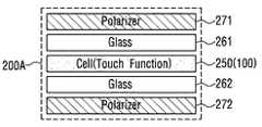
本願明細書において、図面符号200Aは、ディスプレイモジュール200に含まれたディスプレイパネルを指し示す。図2に示されたように、LCDパネル200Aは、液晶セル(liquid crystal cell)を含む液晶層250、液晶層250の両端に電極を含む第1ガラス層261と第2ガラス層262、そして前記液晶層250と対向する方向として前記第1ガラス層261の一面に第1偏光層271及び前記第2ガラス層262の一面に第2偏光層272を含んでもよい。該当技術分野の当業者には、LCDパネルがディスプレイ機能を遂行するために他の構成をさらに含んでもよく、変形が可能なことは自明であろう。 In the present specification, a
図2aは、タッチ入力装置1000において、タッチセンサパネル100がディスプレイモジュール200の外部に配置されたことを示す。タッチ入力装置1000に対するタッチ表面は、タッチセンサパネル100の表面であってもよい。図2aにおいて、タッチ表面になり得るタッチセンサパネル100の面は、タッチセンサパネル100の上部面になってもよい。また、実施形態によりタッチ入力装置1000に対するタッチ表面は、ディスプレイモジュール200の外面になってもよい。図2aにおいて、タッチ表面になり得るディスプレイモジュール200の外面は、ディスプレイモジュール200の第2偏光層272の下部面になってもよい。この時、ディスプレイモジュール200を保護するために、ディスプレイモジュール200の下部面はガラスのようなカバー層(図示せず)で覆われていてもよい。 FIG. 2 a illustrates that the
図2b及び2cは、タッチ入力装置1000において、タッチセンサパネル100がディスプレイパネル200Aの内部に配置されたことを示す。この時、図2bにおいては、タッチ位置を検出するためのタッチセンサパネル100が、第1ガラス層261と第1偏光層271との間に配置されている。この時、タッチ入力装置1000に対するタッチ表面は、ディスプレイモジュール200の外面として図2bで上部面又は下部面になってもよい。図2cにおいては、タッチ位置を検出するためのタッチセンサパネル100が、液晶層250に含まれて具現される場合を例示する。この時、タッチ入力装置1000に対するタッチ表面は、ディスプレイモジュール200の外面として図2cで上部面又は下部面になってもよい。図2b及び図2cにおいて、タッチ表面になり得るディスプレイモジュール200の上部面又は下部面は、ガラスのようなカバー層(図示せず)で覆われていてもよい。 2b and 2c show that the
以上においては、本発明の実施形態によるタッチセンサパネル100に対するタッチの有無及び/又はタッチの位置を検出することを説明したが、本発明の実施形態によるタッチセンサパネル100を用いてタッチの有無及び/又は位置と共にタッチの圧力の大きさを検出することができる。また、タッチセンサパネル100と別個にタッチ圧力を検出する圧力検出モジュールをさらに含んで、タッチの圧力の大きさを検出することも可能である。 In the above description, the presence / absence of touch and / or the position of the touch on the
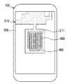
図3は、本発明の第1実施形態により、タッチ位置及びタッチ圧力を検出できるように構成されたタッチ入力装置の断面図である。 FIG. 3 is a cross-sectional view of a touch input device configured to detect a touch position and a touch pressure according to the first embodiment of the present invention.
ディスプレイモジュール200を含むタッチ入力装置1000において、タッチ位置を検出するためのタッチセンサパネル100及び圧力検出モジュール400は、ディスプレイモジュール200の前面に付着されてもよい。これにより、ディスプレイモジュール200のディスプレイスクリーンを保護して、タッチセンサパネル100のタッチ検出の感度を高めることができる。 In the
この時、圧力検出モジュール400は、タッチ位置を検出するためのタッチセンサパネル100と別個に動作することもできるので、例えば、圧力検出モジュール400は、タッチ位置を検出するためのタッチセンサパネル100と独立して圧力だけを検出するように構成されてもよい。また、圧力検出モジュール400は、タッチ位置を検出するためのタッチセンサパネル100と結合してタッチ圧力を検出するように構成されてもよい。例えば、タッチ位置を検出するためのタッチセンサパネル100に含まれた駆動電極TXと受信電極RXのうち少なくとも一つの電極は、タッチ圧力を検出するのに用いられてもよい。 At this time, the
図3において、圧力検出モジュール400は、タッチセンサパネル100と結合してタッチ圧力を検出できる場合を例示する。図3において、圧力検出モジュール400は、前記タッチセンサパネル100とディスプレイモジュール200との間を離隔させるスペーサ層420を含む。圧力検出モジュール400は、スペーサ層420を通じてタッチセンサパネル100と離隔した基準電位層を含んでもよい。この時、ディスプレイモジュール200は、基準電位層として機能することができる。 In FIG. 3, the
基準電位層は、駆動電極TXと受信電極RXとの間に生成された静電容量101に変化を引き起こさせるようにする任意の電位を有してもよい。例えば、基準電位層は、グランド(ground)電位を有するグランド層であってもよい。基準電位層は、ディスプレイモジュール200のグランド(ground)層であってもよい。この時、基準電位層は、タッチセンサパネル100の2次元平面と平行した平面を有してもよい。 The reference potential layer may have an arbitrary potential that causes a change in the
図3に示されたように、タッチセンサパネル100と基準電位層であるディスプレイモジュール200とは、離隔して位置する。この時、タッチセンサパネル100とディスプレイモジュール200の接着方法の差によって、タッチセンサパネル100とディスプレイモジュール200との間のスペーサ層420は、エアギャップ(air gap)で具現されてもよい。スペーサ層420は、実施形態により衝撃吸収物質からなってもよい。スペーサ層420は、実施形態により誘電物質(dielectric material)で満たされてもよい。 As shown in FIG. 3, the
この時、タッチセンサパネル100とディスプレイモジュール200とを固定するために、両面接着テープ430(DAT:Double Adhesive Tape)が用いられてもよい。例えば、タッチセンサパネル100とディスプレイモジュール200は、それぞれの面積が重ねられた形態であり、タッチセンサパネル100とディスプレイモジュール200それぞれの端領域において両面接着テープ430を介して二つの層が接着されるが、残りの領域においてタッチセンサパネル100とディスプレイモジュール200とが所定の距離dに離隔されてもよい。 At this time, in order to fix the
一般的に、タッチセンサパネル100の撓みなしにタッチ表面をタッチする場合でも、駆動電極TXと受信電極RXとの間の静電容量101:Cmが変化する。すなわち、タッチセンサパネル100に対するタッチの際に、相互静電容量Cm:101が基本相互静電容量に比べて減少する。これは指のような導体である客体がタッチセンサパネル100に近接した場合、客体がグランドGNDの役割をして相互静電容量Cm:101のフリンジング静電容量(fringing capacitance)が客体に吸収されるためである。基本相互静電容量は、タッチセンサパネル100に対するタッチがない場合に、駆動電極TXと受信電極RXとの間の相互静電容量の値である。 In general, even when the touch surface is touched without bending the
タッチセンサパネル100のタッチ表面である上部表面を客体でタッチする際に圧力が加えられた場合、タッチセンサパネル100が撓む。この時、駆動電極TXと受信電極RXとの間の相互静電容量101:Cmの値はさらに減少する。これは、タッチセンサパネル100が撓んでタッチセンサパネル100と基準電位層との間の距離がdからd’に減少することによって、前記相互静電容量101:Cmのフリンジング静電容量が客体だけでなく基準電位層にも吸収されるためである。タッチの客体が不導体である場合には、相互静電容量Cmの変化は、単にタッチセンサパネル100と基準電位層との間の距離変化d−d’のみに起因してもよい。 When pressure is applied when the upper surface, which is the touch surface of the
以上で詳しく見たように、ディスプレイモジュール200上にタッチセンサパネル100及び圧力検出モジュール400を含んでタッチ入力装置1000を構成することによって、タッチ位置だけでなくタッチ圧力を同時に検出することができる。 As described in detail above, by configuring the
しかし、図3に示されたように、タッチセンサパネル100だけでなく圧力検出モジュール400までディスプレイモジュール200の上部に配置させる場合、ディスプレイモジュールのディスプレイ特性が低下する問題点が発生する。特に、ディスプレイモジュール200の上部にエアギャップ420を含む場合に、ディスプレイモジュールの視認性及び光透過率が低下することがある。 However, as shown in FIG. 3, when not only the
したがって、このような問題点が発生することを防止するために、タッチ位置を検出するためのタッチセンサパネル100とディスプレイモジュール200との間にエアギャップを配置せずに、OCA(Optically Clear Adhesive)のような接着剤でタッチセンサパネル100とディスプレイモジュール200とが完全ラミネーション(lamination)されてもよい。 Accordingly, in order to prevent the occurrence of such a problem, an optical gap is not provided between the
図4aは、本発明の第2実施形態によるタッチ入力装置の断面図である。本発明の第2実施形態によるタッチ入力装置1000において、タッチ位置を検出するためのタッチセンサパネル100とディスプレイモジュール200との間が接着剤で完全ラミネーションされる。これによりタッチセンサパネル100のタッチ表面を通じて確認できるディスプレイモジュール200のディスプレイの色の鮮明度、視認性、及び光透過性が向上してもよい。 FIG. 4a is a cross-sectional view of a touch input device according to a second embodiment of the present invention. In the
図4a、図4b及び図5、そしてこれを参照した説明において、本発明の第2実施形態によるタッチ入力装置1000として、タッチセンサパネル100がディスプレイモジュール200上に接着剤でラミネーションされて付着したものを例示するが、本発明の第2実施形態によるタッチ入力装置1000は、タッチセンサパネル100が図2b及び図2cなどに示されたように、ディスプレイモジュール200の内部に配置される場合も含んでいてもよい。より具体的に、図4a、図4b及び図5において、タッチセンサパネル100がディスプレイモジュール200を覆うことが示されているが、タッチセンサパネル100はディスプレイモジュール200の内部に位置して、ディスプレイモジュール200がガラスのようなカバー層で覆われたタッチ入力装置1000が、本発明の第2実施形態に用いられてもよい。 4a, 4b and 5, and the description with reference thereto, the
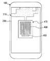
本発明の実施形態によるタッチ入力装置1000は、携帯電話(cell phone)、PDA(Personal Data Assistant)、スマートフォン(smartphone)、タブレットPC(taplet Personal Computer)、MP3プレーヤー、ノートブック(notebook)などのようなタッチスクリーンを含む電子装置を含んでもよい。 The
本発明の実施形態によるタッチ入力装置1000において、基板300は、例えばタッチ入力装置1000の最外郭をなす機構であるカバー320と共にタッチ入力装置1000の作動のための回路基板及び/又はバッテリーが位置することができる実装空間310などを覆うハウジング(housing)の機能を遂行することができる。この時、タッチ入力装置1000の作動のための回路基板には、メインボード(main board)として中央処理ユニットであるCPU(central processing unit)又はAP(application processor)などが実装されていてもよい。基板300を通じてディスプレイモジュール200とタッチ入力装置1000の作動のための回路基板及び/又はバッテリーが分離し、ディスプレイモジュール200で発生する電気的ノイズが遮断されてもよい。 In the
タッチ入力装置1000において、タッチセンサパネル100又は前面カバー層が、ディスプレイモジュール200、基板300、及び実装空間310より広く形成されてもよく、これによりカバー320がタッチセンサパネル100と共にディスプレイモジュール200、基板300及び回路基板310を覆うように、カバー320が形成されてもよい。 In the
本発明の第2実施形態によるタッチ入力装置1000は、タッチセンサパネル100を通じてタッチ位置を検出し、ディスプレイモジュール200と基板300との間に圧力検出のための電極450、460を配置してタッチ圧力を検出することができる。この時、タッチセンサパネル100は、ディスプレイモジュール200の内部又は外部に位置することができる。本発明の第2実施形態によるタッチ入力装置1000においては、別途のスペーサ層及び/又は基準電位層を製作することなしに、ディスプレイモジュール200の内部又は外部に存在するエアギャップ(air gap)及び/又は電位層を用いてタッチ圧力を検出することができ、これに対しては図4bないし図7bを参照して詳しく見てみる。 The
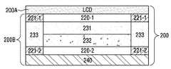
図4bは、本発明の第2実施形態によるタッチ入力装置1000に含まれ得るディスプレイモジュール200の例示的な断面図である。図4bでは、ディスプレイモジュール200としてLCDモジュールを例示する。図4bに示されたように、LCDモジュール200は、LCDパネル200Aとバックライトユニット200B(backlight unit)を含んで構成されてもよい。LCDパネル200Aは、それ自体が発光できず、ただし、光を遮断ないし透過させる機能を遂行する。したがって、LCDパネル200Aの下部には光源が位置して、LCDパネル200Aに光を照らし、画面には明るさと暗さだけでなく多様な色を有する情報を表現するようになる。LCDパネル200Aは、受動素子として自ら発光できないので、後面に均一な輝度分布を有する光源が要求される。LCDパネル200A及びバックライトユニット200Bの構造及び機能は公示された技術であり、以下で簡単に見てみる。 FIG. 4b is an exemplary cross-sectional view of a
LCDパネル200Aのためのバックライトユニット200Bは、数個の光学的部品(optical part)を含んでもよい。図4bにおいて、バックライトユニット200Bは、光拡散及び光向上シート231、導光板232、及び反射板240を含んでもよい。この時、バックライトユニット200Bは、線光源(linear light source)又は点光源(point light source)などの形態として、導光板232の後面及び/又は側面に配置された光源(図示せず)を含んでもよい。実施形態により、導光板232と光拡散及び光向上シート231の端に支持部233をさらに含んでもよい。 The
導光板232(light guide plate)は、一般的に、線光源又は点光源の形態である光源(図示せず)から光を面光源の形態に変換してLCDパネル200Aに向かうようにする役割をすることができる。 The
導光板232から放出される光の一部がLCDパネル200Aの反対面に放出されて損失することがある。反射板240は、このような損失した光を導光板232に再入射させられるように、導光板232の下部に位置して反射率が高い物質で構成されてもよい。 A part of the light emitted from the
光拡散及び光向上シート231は、拡散シート(diffuser sheet)及び/又はプリズムシート(prism sheet)を含んでもよい。拡散シートは、導光板232から入射される光を拡散させる役割をする。例えば、導光板232のパターン(pattern)によって散乱した光は直接目に入ってくるため、導光板232のパターンがそのまま映るようになり得る。さらに、このようなパターンは、LCDパネル200Aを装着した後にも確然として感知できるので、拡散シートはこのような導光板232のパターンを相殺させる役割を遂行することができる。 The light diffusion and
拡散シートを過ぎると光の輝度は急激に落ちることになる。したがって、光を再びフォーカス(focus)させて光の輝度を向上させるようにプリズムシートが含まれてもよい。 After passing through the diffusion sheet, the brightness of the light drops sharply. Therefore, a prism sheet may be included so as to focus the light again and improve the brightness of the light.
バックライトユニット200Bは、技術の変化、発展及び/又は実施形態により前述した構成と異なる構成を含んでもよく、また、前述した構成以外に追加的な構成をさらに含んでもよい。また、本発明の実施形態によるバックライトユニット200Bは、例えば、バックライトユニット200Bの光学的構成を外部の衝撃や異物流入による汚染などから保護するために、保護シート(protection sheet)をプリズムシートの上部にさらに含んでもよい。また、バックライトユニット200Bは、光源からの光損失を最小化にするため、実施形態によりランプカバー(lamp cover)をさらに含んでもよい。また、バックライトユニット200Bは、バックライトユニット200Bの主要構成である導光板232、シート231、及びランプ(図示せず)などが許容寸法に合うように、正確に分離組立が可能なようにする形態を維持するようにするフレーム(frame)をさらに含んでもよい。また、前述した構成それぞれは、2以上の別個の部分から成ってもよい。例えば、プリズムシートは、2つのプリズムシートで構成されてもよい。 The
この時、導光板232と反射板240との間には、第1エアギャップ220−2が存在するように構成されてもよい。これにより、導光板232から反射板240への損失光が反射板240を通じて再び導光板232に再入射されてもよい。この時、エアギャップ220−2を維持できるように、導光板232と反射板240との間として、端には両面接着テープ221−2が含まれてもよい。 At this time, the first air gap 220-2 may exist between the
また、実施形態によりバックライトユニット200Bは、LCDパネル200Aと第2エアギャップ220−1を挟んで位置してもよい。これは、LCDパネル200Aからの衝撃がバックライトユニット200Bに伝達されるのを防止するためである。この時、エアギャップ220−1を維持できるようにバックライトユニット200BとLCDパネル200Aとの間として、端には両面接着テープ221−1が含まれてもよい。 Further, according to the embodiment, the
以上で詳しく見たように、ディスプレイモジュール200は、独自に第1エアギャップ220−2及び/又は第2エアギャップ220−1のようなエアギャップを含んで構成されてもよい。または、光拡散及び光向上シート231の複数のレイヤー間にエアギャップが含まれてもよい。以上では、LCDモジュールの場合に対して説明したが、他のディスプレイモジュールの場合にも構造内にエアギャップを含んでもよい。 As described in detail above, the
したがって、本発明の第3実施形態によるタッチ入力装置1000は、圧力検出のために別途のスペーサ層を製作することなしに、ディスプレイモジュール200の内または外にすでに存在するエアギャップを使用することができる。スペーサ層として用いられるエアギャップは、図4bを参照して説明される第1エアギャップ220−2及び/又は第2エアギャップ220−1だけでなく、ディスプレイモジュール200内に含まれる任意のエアギャップであってもよい。または、ディスプレイモジュール200の外部に含まれるエアギャップであってもよい。このように、圧力を検出できるタッチ入力装置1000を製造することで製造費用を節減し、及び/又は、製造工程を簡素化することができる。 Accordingly, the
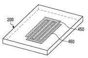
図5は、本発明の第2実施形態によるタッチ入力装置の斜視図である。図5に示されたように、本発明の実施形態によるタッチ入力装置1000において、ディスプレイモジュール200と基板300との間に位置する圧力検出のための電極450及び460を含んでもよい。以下で、タッチセンサパネル100に含まれた電極と区分が明確になるように、圧力を検出するための電極450及び460を圧力電極450及び460と指称する。この時、圧力電極450及び460は、ディスプレイパネルの前面でない後面に含まれるので、透明物質だけでなく不透明物質で構成されることも可能である。図6aは、本発明の第1実施形態による圧力電極パターンを含むタッチ入力装置の断面図である。図6aに示されたように、本発明の第1実施形態による圧力電極450、460は、ディスプレイモジュール200と基板300との間で、基板300上に形成されてもよい。図6aないし図6f及び図7aにおいて、便宜のために圧力電極450、460の厚さが誇張されて厚く示されているが、圧力電極450、460はシート(sheet)形態で具現され得るので、当該厚さは非常に小さくてもよい。同様に、ディスプレイモジュール200と基板300との間の間隔もまた誇張されて広く示されているが、この二つの間の間隔もまた非常に小さい間隔を有するように具現されてもよい。図6a及び図6bにおいて、圧力電極450、460が基板300上に形成されたことを示すために、圧力電極450、460とディスプレイモジュール200との間が離隔するように示したが、これは単に説明のためのものであり、これらの間は離隔しないように具現されてもよい。 FIG. 5 is a perspective view of a touch input device according to a second embodiment of the present invention. As shown in FIG. 5, the
圧力検出のための圧力電極は、第1電極450と第2電極460とを含んでもよい。この時、第1電極450と第2電極460のうち、いずれか一つは駆動電極であってもよく、残りの一つは受信電極であってもよい。駆動電極に駆動信号を印加して受信電極を通じて感知信号を獲得することができる。電圧が印加されると、第1電極450と第2電極460との間に相互静電容量が生成されてもよい。 The pressure electrode for pressure detection may include a
この時、図6aにおいては、ディスプレイモジュール200がスペーサ層220及び基準電位層270を含むように示される。 At this time, in FIG. 6 a, the
スペーサ層220は、図4bを参照して説明されたように、ディスプレイモジュール200の製造の際に含まれる第1エアギャップ220−2及び/又は第2エアギャップ220−1であってもよい。ディスプレイモジュール200が一つのエアギャップを含む場合、当該一つのエアギャップがスペーサ層220の機能を遂行することができ、ディスプレイモジュール200が複数個のエアギャップを含む場合、当該複数個のエアギャップが統合的にスペーサ層220の機能を遂行することができる。図6aないし図6c及び図7aにおいては、機能的に一つのスペーサ層220を含むように示される。 The
本発明の実施形態によるタッチ入力装置1000は、図2aないし図2cにおいて、ディスプレイモジュール200の内部として、スペーサ層220より上部に基準電位層270を含んでもよい。このような基準電位層270もまたディスプレイモジュール200の製造時に、独自に含まれるグランド電位層であってもよい。例えば、図2aないし図2cに示されたディスプレイパネル200Aにおいて、第1偏光層271と第1ガラス層261との間にノイズ(noise)遮蔽のための電極(図示せず)を含んでもよい。このような遮蔽のための電極はITOで構成されてもよく、グランドの役割を遂行することができる。このような基準電位層270は、ディスプレイモジュール200の内部として、前記基準電位層270と圧力電極450、460との間にスペーサ層220が位置するようにする任意の所に位置することができ、以上で例示した遮蔽電極以外の任意の電位を有する電極が基準電位層270として用いられてもよい。例えば、基準電位層270は、ディスプレイモジュール200の共通電極電位(Vcom)層であってもよい。 The
特に、タッチ入力装置1000を含む装置の厚さを薄くしようとする努力の一環として、別途のカバー又はフレーム(frame)を通じてディスプレイモジュール200を覆うように構成しなくてもよい。このような場合、基板300と向かい合うディスプレイモジュール200の下部面は、反射板240及び/又は不導体であってもよい。このような場合、ディスプレイモジュール200の下部面は、グランド電位を有することはできない。このようにディスプレイモジュール200の下部面が基準電位層として機能できない場合にも、本発明の実施形態によるタッチ圧力装置1000を用いれば、ディスプレイモジュール200の内部に位置する任意の電位層を基準電位層270として用いて圧力を検出することができる。 In particular, as part of efforts to reduce the thickness of the device including the
図6bは、図6aに示されたタッチ入力装置1000に圧力が印加された場合の断面図である。客体500を通じてタッチセンサパネル100の表面に圧力を印加する場合、タッチセンサパネル100及びディスプレイモジュール200は、撓んだり押されてもよい。この時、ディスプレイモジュール200内に位置したスペーサ層220により、基準電位層270と圧力電極パターン450、460との間の距離dがd’に減少する。このような場合、前記距離dの減少により基準電位層270にフリンジング静電容量が吸収されるので、第1電極450と第2電極460との間の相互静電容量は減少する。したがって、受信電極を通じて取得される感知信号において、相互静電容量の減少量を取得してタッチ圧力の大きさを算出することができる。 FIG. 6B is a cross-sectional view when a pressure is applied to the
この時、タッチ圧力の大きさが十分に大きい場合、所定の位置で基準電位層270と圧力電極パターン450、460との間の距離がこれ以上近づかない状態に至ってもよい。このような状態を、以下では飽和状態と指称する。しかし、このような場合にも、タッチ圧力の大きさがさらに大きくなる時には、基準電位層270と圧力電極パターン450、460との間の距離がこれ以上近づかない飽和状態にある面積が大きくなり得る。このような面積が大きくなるほど、第1電極450と第2電極460との間の相互静電容量は減少する。以下で、距離の変化に伴う静電容量の変化に従ってタッチ圧力の大きさを算出することが説明されるが、これは飽和状態にある飽和面積の変化に従ってタッチ圧力の大きさを算出することを含んでもよい。 At this time, when the magnitude of the touch pressure is sufficiently large, the distance between the reference
本発明の実施形態によるタッチ入力装置1000において、ディスプレイモジュール200は、圧力を印加するタッチによって撓んだり押されてもよい。ディスプレイモジュール200は、タッチの位置で最も大きい変形を示すように撓んだり押されてもよい。実施形態によりディスプレイモジュール200が撓んだり押されるとき、最も大きい変形を示す位置は、前記タッチ位置と一致しないこともあるが、ディスプレイモジュール200は、少なくとも前記タッチ位置で撓み又は押されることを示すことができる。例えば、タッチ位置がディスプレイモジュール200の縁や端などに近接する場合、ディスプレイモジュール200が撓んだり押される程度が最も大きい位置はタッチ位置と異なることもあるが、ディスプレイモジュール200は、少なくとも前記タッチ位置で撓み又は押されることを示すことができる。 In the
この時、タッチ入力装置1000に対するタッチの際に、ディスプレイモジュール200が撓んだり押されるとき、図6bに示されたように、スペーサ層220によってスペーサ層220の下部に位置した層(例えば、反射板)の撓み又は押されることは無いか、もしくは減少し得る。図6bにおいては、ディスプレイモジュール200の最下部では撓み又は押されることが全くないよう示されたが、これは例示に過ぎず、ディスプレイモジュール200の最下部でも撓み又は押されることがあり得るが、スペーサ層220を通じてその程度が緩和され得る。 At this time, when the
この時、基板300の上部面もまたノイズ遮蔽のためにグランド電位を有してもよい。したがって、基板300と圧力電極450、460が短絡(short circuit)することを防止するために、圧力電極450、460は絶縁層470上に形成されてもよい。図8は、本発明の実施形態による圧力電極の付着構造を例示する。図8(a)を参照して説明すると、圧力電極450、460は、基板300上に第1絶縁層470を位置させた後、圧力電極450、460を形成して構成されてもよい。また、実施形態により圧力電極450、460が形成された第1絶縁層470を基板300上に付着して形成することができる。また、実施形態により圧力電極は、基板300又は基板300上の第1絶縁層470上に圧力電極パターンに相応する貫通孔を有するマスク(mask)を位置させた後、伝導性スプレー(spray)を噴射することによって形成されてもよい。 At this time, the upper surface of the
また、ディスプレイモジュール200の下部面がグランド電位を有する場合、基板300上に位置した圧力電極450、460とディスプレイモジュール300とが短絡するのを防止するために、圧力電極450、460は追加の第2絶縁層471で圧力電極450、460を覆うことができる。また、第1絶縁層470上に形成された圧力電極450、460を追加の第2絶縁層471で覆った後、一体型で基板300上に付着して圧力検出モジュール400を形成することができる。 In addition, when the lower surface of the
図8(a)を参照して説明された圧力電極450、460の付着構造及び方法は、圧力電極450、460がディスプレイモジュール200に付着する場合にも適用されてもよい。圧力電極450、460がディスプレイモジュール200に付着する場合は、図6fと関連してさらに詳しく説明される。 The attachment structure and method of the
また、タッチ入力装置1000の種類及び/又は具現方式により、圧力電極450、460が付着する基板300又はディスプレイモジュール200がグランド電位を示さないか、もしくは弱いグランド電位を示してもよい。このような場合、本発明の実施形態によるタッチ入力装置1000は、基板300又はディスプレイモジュール200と絶縁層470との間にグランド電極(ground electrode:図示せず)をさらに含んでもよい。実施形態により、グランド電極と基板300又はディスプレイモジュール200との間には、また別の絶縁層(図示せず)をさらに含んでもよい。この時、グランド電極(図示せず)は、圧力電極である第1電極450と第2電極460との間に生成される静電容量の大きさが非常に大きくなるのを防止することができる。 Further, depending on the type and / or implementation method of the
以上で説明した圧力電極450、460の形成及び付着方法は、以下の実施形態にも同様に適用されてもよい。 The method for forming and attaching the
図6cは、本発明の第1実施形態の変形例による圧力電極パターンを含むタッチ入力装置の断面図である。図6cにおいては、スペーサ層420がディスプレイモジュール200と基板300との間に位置する場合を例示する。ディスプレイモジュール200を含むタッチ入力装置1000を製造するとき、ディスプレイモジュール200と基板300との間は完全に付着されないので、エアギャップ420が発生することがある。ここで、このようなエアギャップ420をタッチ圧力検出のためのスペーサ層として用いることにより、タッチ圧力検出のためにわざとスペーサ層を製作する時間・費用を節減することができる。ディスプレイモジュール200と基板300は、図6c及び図6dではスペーサ層として用いられるエアギャップ220がディスプレイモジュール200の内部に位置しないように示されているが、図6c及び図6dでは、追加でエアギャップ220がディスプレイモジュール200内に含まれる場合も含まれてもよい。 FIG. 6c is a cross-sectional view of a touch input device including a pressure electrode pattern according to a modification of the first embodiment of the present invention. FIG. 6 c illustrates a case where the
図6は、図6cに示されたタッチ入力装置に圧力が印加された場合の断面図である。図6bと同様にタッチ入力装置1000に対するタッチの際にディスプレイモジュール200が撓んだり押されてもよい。この時、基準電位層270と圧力電極450、460との間に位置するスペーサ層420により、基準電位層270と圧力電極パターン450、460との間の距離dがd’に減少する。このような場合、前記距離dの減少により基準電位層270にフリンジング静電容量が吸収されるので、第1電極450と第2電極460との間の相互静電容量は減少する。したがって、受信電極を通じて取得される感知信号において、相互静電容量の減少量を取得してタッチ圧力の大きさを算出することができる。 6 is a cross-sectional view when pressure is applied to the touch input device shown in FIG. 6c. Similar to FIG. 6b, the
図6eは、本発明の第2実施形態による圧力電極を含むタッチ入力装置の断面図である。第1実施形態において、圧力電極450、460が基板300上に形成されたことが例示されているが、圧力電極450、460は、ディスプレイモジュール200の下部面上に形成されても構わない。タッチセンサパネルのタッチ表面をタッチすることにより、基準電位層270と圧力電極450、460との間の距離dが減少して、結果的に第1電極450と第2電極460との間の相互静電容量の変化を引き起こすことができる。図6eでは、圧力電極450、460がディスプレイモジュール200上に付着することを説明するために、圧力電極450、460と基板300との間が離隔するように示したが、これは単に説明のためのものであり、この二つの間は離隔しないように構成されてもよい。もちろん、図6c及び図6dと同様にディスプレイモジュール200と基板300との間はスペーサ層420で離隔されてもよい。 FIG. 6e is a cross-sectional view of a touch input device including a pressure electrode according to a second embodiment of the present invention. In the first embodiment, it is exemplified that the
図6fは、本発明の第1実施形態による圧力電極パターンを例示する。図6dでは、第1電極450と第2電極460とが基板300上に形成された場合を示す。第1電極450と第2電極460との間の静電容量は、基準電位層270と圧力電極450、460との間の距離によって変わり得る。 FIG. 6f illustrates a pressure electrode pattern according to the first embodiment of the present invention. FIG. 6 d shows a case where the
図6gは、本発明の第2実施形態による圧力電極パターンを例示する。図6gにおいて、圧力電極450、460は、ディスプレイモジュール200の下部面上に形成された場合を示す。 FIG. 6g illustrates a pressure electrode pattern according to a second embodiment of the present invention. In FIG. 6 g, the
図6h及び図6iは、本発明の実施形態に適用され得る圧力電極パターン450、460を例示する。第1電極450と第2電極460との間の相互静電容量が変化することによってタッチ圧力の大きさを検出する時、検出の正確度を高めるために必要な静電容量の範囲を生成するように、第1電極450と第2電極460のパターンを形成する必要がある。第1電極450と第2電極460とが互いに向かい合う面積が大きいか、もしくは長さが長いほど、生成される静電容量の大きさが大きくなってもよい。したがって、必要な静電容量の範囲により、第1電極450と第2電極460との間の向かい合う面積の大きさ、長さ及び形状などを調節して設計することができる。図6h及び図6iには、第1電極450と第2電極460とが同一の層に形成される場合として、第1電極450と第2電極460とが互いに向かい合う長さが相対的に長いように圧力電極が形成された場合を例示する。 6h and 6i illustrate
第1実施形態と第2実施形態において、第1電極450と第2電極460は、同一の層に形成されたもので示されているが、第1電極450と第2電極460は、実施形態により互いに異なる層に具現されても構わない。図8(b)は、第1電極450と第2電極460とが互いに異なる層に具現された場合の付着構造を例示する。図8(b)に例示されたように、第1電極450は第1絶縁層470上に形成され、第2電極460は第1電極450上に位置する第2絶縁層471上に形成されてもよい。実施形態により、第2電極460は第3絶縁層472で覆われてもよい。この時、第1電極450と第2電極460とは互いに異なる層に位置するので、互いにオーバーラップ(overlap)するように具現されてもよい。例えば、第1電極450と第2電極460とは、図1を参照して説明されたタッチセンサパネル100に含まれたMXNの構造で配列された駆動電極TXと受信電極RXのパターンと類似するように形成されてもよい。この時、M及びNは、1以上の自然数であってもよい。 In the first embodiment and the second embodiment, the
第1実施形態において、タッチ圧力は、第1電極450と第2電極460との間の相互静電容量の変化から検出されることが例示される。しかし、圧力電極450、460が第1電極450と第2電極460の何れか一つの圧力電極のみを含むように構成されてもよく、このような場合、一つの圧力電極と基準電位層270との間の静電容量の変化を検出することによって、タッチ圧力の大きさを検出することもできる。 In the first embodiment, it is exemplified that the touch pressure is detected from a change in mutual capacitance between the
例えば、図6a及び図6cにおいて、圧力電極は第1電極450のみを含んで構成されてもよく、この時、基準電位層270と第1電極450との間の距離変化によって引き起こされる第1電極450と基準電位層270との間の静電容量の変化からタッチ圧力の大きさを検出することができる。タッチ圧力が大きくなることによって距離dが減少するので、基準電位層270と第1電極450との間の静電容量は、タッチ圧力が増加するほど大きくなり得る。これは、図6eと関連した実施形態にも同様に適用されてもよい。この時、圧力電極は、相互静電容量の変化量の検出精度を高めるために必要な、くし形状又はフォーク形状を有する必要はなく、板(例えば、四角板)形状を有してもよい。 For example, in FIGS. 6a and 6c, the pressure electrode may include only the
図8(c)は、圧力電極が第1電極450のみを含んで具現された場合の付着構造を例示する。図8(c)に例示されたように、第1電極450は、基板300又はディスプレイモジュール200上に位置した第1絶縁層470上に形成されてもよい。また、実施形態により第1電極450は第2絶縁層471で覆われてもよい。 FIG. 8C illustrates an attachment structure when the pressure electrode is implemented to include only the
図7aは、本発明の第3実施形態による圧力電極を含むタッチ入力装置の断面図である。本発明の第3実施形態による圧力電極450、460は、基板300の上部面及びディスプレイモジュール200の下部面上に形成されてもよい。 FIG. 7a is a cross-sectional view of a touch input device including a pressure electrode according to a third embodiment of the present invention. The
圧力検出のための圧力電極パターンは、第1電極450と第2電極460を含んでもよい。この時、第1電極450と第2電極460の何れか一つは基板300上に形成され、残りの一つはディスプレイモジュール200の下部面上に形成されてもよい。図7aにおいては、第1電極450が基板300上に形成され、第2電極460がディスプレイモジュール200の下部面上に形成されたことを例示する。図7aにおいては、第1電極450と第2電極460との間が離隔されるように示されているが、これはただ第1電極450が基板300上に形成され、第2電極460がディスプレイモジュール200上に形成されたことを説明するためのものであり、この二つの間にはエアギャップで離隔したり、この二つの間に絶縁物質が位置したり、又は第1電極450と第2電極460とは互いに重ならないように、例えば同一な層に形成される場合と同様に横にずれるように形成されてもよい。 The pressure electrode pattern for pressure detection may include a
客体500を通じてタッチセンサパネル100の表面に圧力を印加する場合、タッチセンサパネル100及びディスプレイモジュール200は、撓んだり押されてもよい。これにより第1電極450及び第2電極460と基準電位層270との間の距離dが減少する。このような場合、前記距離dの減少により、第1電極450と第2電極460との間の相互静電容量は減少する。したがって、受信電極を通じて取得される感知信号において、相互静電容量の減少量を取得してタッチ圧力の大きさを算出することができる。 When pressure is applied to the surface of the
図7bは、本発明の第3実施形態による圧力電極パターンを例示する。図7bでは、第1電極450が基板300の上部面上に形成され、第2電極460がディスプレイモジュール200の下部面に形成されたことが示される。図7bに示されたように、第1電極450と第2電極460とが互いに直交するように配置して、静電容量の変化量の感知感度が向上し得る。 FIG. 7b illustrates a pressure electrode pattern according to a third embodiment of the present invention. FIG. 7 b shows that the
図8(d)は、第1電極450が基板300上に付着し、第2電極460がディスプレイモジュール200に付着した場合の付着構造を例示する。図8(d)に例示されたように、第1電極450は、基板300上に形成された第1絶縁層470−2上に位置し、第1電極450は第2絶縁層471−2によって覆われていてもよい。また、第2電極460はディスプレイモジュール200の下部面上に形成された第1絶縁層470−1上に位置し、第2電極460は第2絶縁層471−1によって覆われていてもよい。 FIG. 8D illustrates an attachment structure when the
図8(a)と関連して説明されたことと同様に、圧力電極450、460が付着する基板300又はディスプレイモジュール200がグランド電位を示さないか、もしくは弱いグランド電位を示す場合、図8(a)ないし図8(d)において第1絶縁層470、470−1、470−2の間にグランド電極(図示せず)をさらに含んでもよい。この時、グランド電極(図示せず)と圧力電極450、460が付着する基板300又はディスプレイモジュール200の間には、追加の絶縁層(図示せず)をさらに含んでもよい。 Similar to that described in connection with FIG. 8A, when the
以上で詳しく見たように、本発明の実施形態によるタッチ入力装置1000は、圧力電極450、460で発生する静電容量の変化を感知する。したがって、第1電極450と第2電極460のうち駆動電極には駆動信号が印加される必要があり、受信電極から感知信号を取得して静電容量の変化量からタッチ圧力を算出しなければならない。実施形態により、圧力検出の動作のためのタッチセンシングICを追加で含むことも可能である。このような場合、図1に示されたように、駆動部120、感知部110、及び制御部130と類似した構成を重複して含むようになるので、タッチ入力装置1000の面積及び体積が大きくなる問題点が発生し得る。 As described above in detail, the
実施形態により、タッチ入力装置1000は、圧力検出のためにタッチセンサパネル100の作動のためのタッチ検出装置を通じて駆動信号が印加され、感知信号の入力を受けてタッチ圧力を検出することができる。以下では、第1電極450が駆動電極であり、第2電極460が受信電極である場合を仮定して説明する。 According to the embodiment, the
このために、本発明の実施形態によるタッチ入力装置1000において、第1電極450は駆動部120から駆動信号の印加を受け、第2電極460は感知信号を感知部110に伝達することができる。制御部130は、タッチセンサパネル100のスキャニングを遂行すると共に圧力検出のスキャニングを遂行するようにしたり、又は、制御部130は時分割して第1時間区間にはタッチセンサパネル100のスキャニングを遂行するようにし、第1時間区間とは異なる第2時間区間には圧力検出のスキャニングを遂行するように制御信号を生成することができる。 For this reason, in the
したがって、本発明の実施形態において、第1電極450と第2電極460は、電気的に駆動部120及び/又は感知部110に連結されなければならない。この時、タッチセンサパネル100のためのタッチ検出装置は、タッチセンシングIC150としてタッチセンサパネル100の一端、又は、タッチセンサパネル100と同一の平面上に形成されることが一般的である。圧力電極パターン450、460は、任意の方法でタッチセンサパネル100のタッチ検出装置と電気的に連結されてもよい。例えば、圧力電極パターン450、460は、ディスプレイモジュール200に含まれた第2PCB210を用いてコネクタ(connector)を通じてタッチ検出装置に連結されてもよい。例えば、図5に示されたように、第1電極450と第2電極460からそれぞれ電気的に延びる伝導性トレース451及び461は、第2PCB210などを通じてタッチセンシングIC150まで電気的に連結されてもよい。 Accordingly, in the embodiment of the present invention, the
図9a及び図9bは、本発明の第2実施形態による圧力電極の付着方法を例示する。図9a及び図9bでは、本発明の実施形態による圧力電極450、460がディスプレイモジュール200の下部面に付着される場合を示す。図9a及び図9bにおいて、ディスプレイモジュール200は、下部面の一部にディスプレイパネルの作動のための回路が実装された第2PCB210が示される。 9a and 9b illustrate a pressure electrode deposition method according to a second embodiment of the present invention. 9A and 9B illustrate the case where the
図9aは、第1電極450と第2電極460がディスプレイモジュール200の第2PCB210の一端に連結されるように、圧力電極450、460をディスプレイモジュール200の下部面に付着する場合を例示する。この時、図9aにおいては、第1電極450と第2電極460が絶縁層470上に製作された場合を例示する。圧力電極450、460は絶縁層470上に形成され、一体型シート(sheet)としてディスプレイモジュール200の下部面に付着されてもよい。第2PCB210上には、圧力電極パターン450、460をタッチセンシングIC150などの必要な構成まで電気的に連結できるように導電性パターンが印刷されていてもよい。これに対する詳細な説明は、図10aないし図10cを参照して説明する。図9aに例示された圧力電極パターン450、460の付着方法は、基板300に対しても同様に適用されてもよい。 FIG. 9 a illustrates a case where the
図9bは、第1電極450と第2電極460がディスプレイモジュール200の第2PCB210に一体型で形成された場合を例示する。例えば、ディスプレイモジュール200の第2PCB210の製作時に、第2PCBに一定の面積211を割愛して予めディスプレイパネルの作動のための回路だけでなく、第1電極450と第2電極460に該当するパターンまで印刷することができる。第2PCB210には、第1電極450及び第2電極460をタッチセンシングIC150などの必要な構成まで電気的に連結する導電性パターンが印刷されてもよい。 FIG. 9 b illustrates a case where the
図10aないし図10cは、本発明の第2実施形態による圧力電極をタッチセンシングIC150に連結する方法を例示する。図10aないし図10cにおいて、タッチセンサパネル100がディスプレイモジュール200の外部に含まれた場合として、タッチセンサパネル100のタッチ検出装置がタッチセンサパネル100のための第1PCB160に実装されたタッチセンシングIC150に集積された場合を例示する。 FIGS. 10 a to 10 c illustrate a method of connecting a pressure electrode to the
図10aにおいて、ディスプレイモジュール200に付着された圧力電極450、460が、第1コネクタ121を通じてタッチセンシングIC150まで連結される場合を例示する。図10aに例示されたように、スマートフォンのような移動通信装置においてタッチセンシングIC150は、第1コネクタ(connector)121を通じてディスプレイモジュール200のための第2PCB210に連結される。第2PCB210は、第2コネクタ221を通じてメインボードに電気的に連結されてもよい。したがって、タッチセンシングIC150は、第1コネクタ121及び第2コネクタ221を通じてタッチ入力装置1000の作動のためにCPU又はAPと信号をやり取りすることができる。 10A illustrates a case where the
この時、図10aにおいては、圧力電極450が図9bに例示されたような方式でディスプレイモジュール200に付着されたことが例示されているが、図9aに例示されたような方式で付着した場合にも適用されてもよい。第2PCB210には、圧力電極450、460が第1コネクタ121を通じてタッチセンシングIC150まで電気的に連結され得るように導電性パターンが印刷されていてもよい。 At this time, in FIG. 10a, it is illustrated that the
図10bにおいて、ディスプレイモジュール200に付着された圧力電極450、460が、第3コネクタ471を通じてタッチセンシングIC150まで連結される場合が例示される。図10bにおいて、圧力電極450、460は、第3コネクタ471を通じてタッチ入力装置1000の作動のためのメインボードまで連結され、その後、第2コネクタ221及び第1コネクタ121を通じてタッチセンシングIC150まで連結されてもよい。この時、圧力電極450、460は、第2PCB210と分離した追加のPCB211上に印刷されてもよい。または、実施形態により圧力電極パターン450、460は絶縁層470上に形成され、圧力電極450、460から伝導性トレースなどを延長させてコネクタ471を通じてメインボードまで連結されてもよい。 FIG. 10B illustrates a case where the
図10cにおいて、圧力電極450、460が第4コネクタ472を通じて直接タッチセンシングIC150に連結される場合が例示される。図10cにおいて、圧力電極450、460は、第4コネクタ472を通じて第1PCB160まで連結されてもよい。第1PCB160には、第4コネクタ472からタッチセンシングIC150まで電気的に連結する導電性パターンが印刷されていてもよい。これにより、圧力電極450、460は、第4コネクタ472を通じてタッチセンシングIC150まで連結されてもよい。この時、圧力電極450、460は、第2PCB210と分離した追加のPCB211上に印刷されてもよい。第2PCB210と追加のPCB211は、互いに短絡しないように絶縁されていてもよい。または、実施形態により圧力電極450、460は絶縁層470上に形成され、圧力電極450、460から伝導性トレースなどを延長させてコネクタ472を通じて第1PCB160まで連結されてもよい。 FIG. 10 c illustrates a case where the
図10b及び図10cの連結方法は、圧力電極450、460がディスプレイモジュール200の下部面だけでなく、基板300上に形成された場合にも適用されてもよい。 10b and 10c may be applied to the case where the
図10aないし図10cにおいては、タッチセンシングIC150が第1PCB160上に形成されたCOF(chip on film)構造を仮定して説明された。しかし、これは単に例示に過ぎず、本発明は、タッチセンシングIC150がタッチ入力装置1000の実装空間310内のメインボード上に実装されるCOB(chip on board)構造の場合にも適用されてもよい。図10aないし図10cに対する説明から、当該技術分野の当業者に、他の実施形態の場合に圧力電極450、460のコネクタを通じた連結は自明であろう。 10A to 10C, the
以上においては、駆動電極として第1電極450が一つのチャネルを構成し、受信電極として第2電極460が一つのチャネルを構成する圧力電極450、460に対して詳しく見てみた。しかし、これは単に例示に過ぎず、実施形態により駆動電極及び受信電極は、それぞれ複数個のチャネルを構成して多重タッチ(multi touch)によって多重の圧力検出が可能であり得る。 In the above, the
図11aないし図11cは、本発明の実施形態による圧力電極が複数のチャネルを構成する場合を例示する。図11aでは、第1電極450−1、450−2と第2電極460−1、460−2それぞれが2個のチャネルを構成する場合が例示される。図11bでは、第1電極450は2個のチャネル450−1、450−2を構成するが、第2電極460は1個のチャネルを構成する場合が例示される。図11cでは、第1電極450−1ないし450−5と第2電極460−1、460−5それぞれが5個のチャネルを構成する場合が例示される。 FIGS. 11 a to 11 c illustrate the case where the pressure electrode according to the embodiment of the present invention constitutes a plurality of channels. FIG. 11 a illustrates a case where each of the first electrodes 450-1 and 450-2 and the second electrodes 460-1 and 460-2 forms two channels. In FIG. 11b, the
図11aないし図11cは、圧力電極が単数又は複数のチャネルを構成する場合を例示して、多様な方法で圧力電極が単数又は複数のチャネルで構成されてもよい。図11aないし図11cにおいて、圧力電極450、460がタッチセンシングIC150に電気的に連結される場合が例示されなかったが、図10aないし図10c及びその他の方法で圧力電極450、460がタッチセンシングIC150に連結されてもよい。 FIGS. 11a to 11c illustrate the case where the pressure electrode constitutes one or more channels, and the pressure electrode may be comprised of one or more channels in various ways. 11A to 11C, the case where the
図12は、本発明の実施形態によるタッチ入力装置1000のタッチ表面中心部を非伝導性客体で加圧する実験を遂行し、客体のグラム重量(gram force)に伴う静電容量の変化量を表示するグラフである。図12から分かるように、本発明の実施形態によるタッチ入力装置1000のタッチ表面中心部を加圧する力が大きくなるほど、圧力検出のための圧力電極パターン450、460の静電容量の変化量が大きくなることが分かる。 FIG. 12 illustrates an experiment in which the center part of the touch surface of the
以上においては、圧力検出のために静電容量方式の検出モジュールが説明されたが、本発明の実施形態によるタッチ入力装置1000は、圧力検出のためにスペーサ層420、
220及び圧力電極450、460を用いる場合であれば、任意の方式の圧力検出モジュールを用いることができる。In the above, the capacitance type detection module has been described for pressure detection. However, the
If 220 and
また、以上において、実施形態を中心に説明したが、これは単に例示に過ぎず、本発明を限定する訳ではなく、本発明が属する分野における通常の知識を有する者であれば、本実施形態の本質的な特徴を外れない範囲で、以上に例示されない様々な変形と応用が可能であることが分かるはずである。例えば、実施形態に具体的に示された各構成要素は、変形して実施することができるものである。そして、このような変形と応用に係る相違点は、添付の特許請求の範囲において規定する本発明の範囲に含まれるものと解釈されるべきである。 In the above description, the embodiment has been mainly described. However, this is merely an example, and does not limit the present invention. Any person having ordinary knowledge in the field to which the present invention belongs will be described. It should be understood that various modifications and applications not exemplified above are possible without departing from the essential characteristics of the above. For example, each component specifically shown in the embodiment can be modified and implemented. Such differences in modification and application should be construed as being included in the scope of the present invention as defined in the appended claims.
1000 タッチ入力装置
100 タッチセンサパネル
110 感知部
120 駆動部
130 制御部
200 ディスプレイモジュール
300 基板
400 圧力検出モジュール
420 スペーサ層
450、460 電極1000
Claims (13)
Translated fromJapaneseディスプレイパネルを含むディスプレイモジュールと、
前記ディスプレイモジュールに直接形成された圧力電極と、
を含み、
前記ディスプレイモジュールは、内部に基準電位層を含み、
前記圧力電極から前記圧力電極と前記基準電位層との間の静電容量によって変化する電気的信号が検出され、
前記静電容量は、前記圧力電極と前記基準電位層との間の相対的な距離変化によって変わり、
前記静電容量に基づいて前記タッチの圧力を検出する、
タッチ入力装置。A touch input device capable of detecting a pressure of a touch on a touch surface,
A display module including a display panel;
A pressure electrode formed directly on the display module;
Including
The display module includes a reference potential layer therein,
From the pressure electrode, an electrical signal that changes due to a capacitance between the pressure electrode and the reference potential layer is detected,
The capacitance is changed by a relative distance change between the pressure electrode and the reference potential layer,
Detecting the pressure of the touch based on the capacitance;
Touch input device.
ディスプレイパネルを含むディスプレイモジュールと、
前記ディスプレイモジュールに一体型で形成された圧力電極と、
を含み、
前記ディスプレイモジュールは、内部に基準電位層を含み、
前記圧力電極から前記圧力電極と前記基準電位層との間の静電容量によって変化する電気的信号が検出され、
前記静電容量は、前記圧力電極と前記基準電位層との間の相対的な距離変化によって変わり、
前記静電容量に基づいて前記タッチの圧力を検出する、
タッチ入力装置。A touch input device capable of detecting a pressure of a touch on a touch surface,
A display module including a display panel;
A pressure electrode formed integrally with the display module;
Including
The display module includes a reference potential layer therein,
From the pressure electrode, an electrical signal that changes due to a capacitance between the pressure electrode and the reference potential layer is detected,
The capacitance is changed by a relative distance change between the pressure electrode and the reference potential layer,
Detecting the pressure of the touch based on the capacitance;
Touch input device.
ディスプレイパネルを含むディスプレイモジュールと、
前記ディスプレイモジュールに印刷された圧力電極と、
を含み、
前記ディスプレイモジュールは、内部に基準電位層を含み、
前記圧力電極から前記圧力電極と前記基準電位層との間の静電容量によって変化する電気的信号が検出され、
前記静電容量は、前記圧力電極と前記基準電位層との間の相対的な距離変化によって変わり、
前記静電容量に基づいて前記タッチの圧力を検出する、
タッチ入力装置。A touch input device capable of detecting a pressure of a touch on a touch surface,
A display module including a display panel;
A pressure electrode printed on the display module;
Including
The display module includes a reference potential layer therein,
From the pressure electrode, an electrical signal that changes due to a capacitance between the pressure electrode and the reference potential layer is detected,
The capacitance is changed by a relative distance change between the pressure electrode and the reference potential layer,
Detecting the pressure of the touch based on the capacitance;
Touch input device.
ディスプレイパネルを含むディスプレイモジュールと、
前記ディスプレイモジュールにパターン化された圧力電極と、
を含み、
前記ディスプレイモジュールは、内部に基準電位層を含み、
前記圧力電極から前記圧力電極と前記基準電位層との間の静電容量によって変化する電気的信号が検出され、
前記静電容量は、前記圧力電極と前記基準電位層との間の相対的な距離変化によって変わり、
前記静電容量に基づいて前記タッチの圧力を検出する、
タッチ入力装置。A touch input device capable of detecting a pressure of a touch on a touch surface,
A display module including a display panel;
A pressure electrode patterned on the display module;
Including
The display module includes a reference potential layer therein,
From the pressure electrode, an electrical signal that changes due to a capacitance between the pressure electrode and the reference potential layer is detected,
The capacitance is changed by a relative distance change between the pressure electrode and the reference potential layer,
Detecting the pressure of the touch based on the capacitance;
Touch input device.
前記ディスプレイモジュールが撓むことによって前記圧力電極と前記基準電位層との間の距離が変わる、請求項1ないし10のいずれか1項に記載のタッチ入力装置。If the pressure is applied, the display module bends,
The touch input device according to claim 1, wherein a distance between the pressure electrode and the reference potential layer is changed by bending the display module.
Applications Claiming Priority (2)
| Application Number | Priority Date | Filing Date | Title |
|---|---|---|---|
| KR10-2014-0124920 | 2014-09-19 | ||
| KR1020140124920AKR101712346B1 (en) | 2014-09-19 | 2014-09-19 | Touch input device |
Related Parent Applications (1)
| Application Number | Title | Priority Date | Filing Date |
|---|---|---|---|
| JP2015146532ADivisionJP6185961B2 (en) | 2014-09-19 | 2015-07-24 | smartphone |
Publications (2)
| Publication Number | Publication Date |
|---|---|
| JP2016105307Atrue JP2016105307A (en) | 2016-06-09 |
| JP5944604B2 JP5944604B2 (en) | 2016-07-05 |
Family
ID=54348657
Family Applications (5)
| Application Number | Title | Priority Date | Filing Date |
|---|---|---|---|
| JP2015124248AActiveJP5798700B1 (en) | 2014-09-19 | 2015-06-19 | smartphone |
| JP2015146532AActiveJP6185961B2 (en) | 2014-09-19 | 2015-07-24 | smartphone |
| JP2015219874AActiveJP6196652B2 (en) | 2014-09-19 | 2015-11-09 | smartphone |
| JP2016014899AActiveJP5944604B2 (en) | 2014-09-19 | 2016-01-28 | smartphone |
| JP2016238146APendingJP2017076421A (en) | 2014-09-19 | 2016-12-08 | smartphone |
Family Applications Before (3)
| Application Number | Title | Priority Date | Filing Date |
|---|---|---|---|
| JP2015124248AActiveJP5798700B1 (en) | 2014-09-19 | 2015-06-19 | smartphone |
| JP2015146532AActiveJP6185961B2 (en) | 2014-09-19 | 2015-07-24 | smartphone |
| JP2015219874AActiveJP6196652B2 (en) | 2014-09-19 | 2015-11-09 | smartphone |
Family Applications After (1)
| Application Number | Title | Priority Date | Filing Date |
|---|---|---|---|
| JP2016238146APendingJP2017076421A (en) | 2014-09-19 | 2016-12-08 | smartphone |
Country Status (6)
| Country | Link |
|---|---|
| US (6) | US9619068B2 (en) |
| EP (3) | EP3037937B1 (en) |
| JP (5) | JP5798700B1 (en) |
| KR (1) | KR101712346B1 (en) |
| CN (8) | CN105446548A (en) |
| WO (1) | WO2016043544A2 (en) |
Families Citing this family (85)
| Publication number | Priority date | Publication date | Assignee | Title |
|---|---|---|---|---|
| US20140253503A1 (en)* | 2013-03-05 | 2014-09-11 | Bang & Olufsen A/S | Touch system configured on metal surface with x-y and force detection |
| US9551783B2 (en)* | 2013-06-03 | 2017-01-24 | Qualcomm Incorporated | Display with backside ultrasonic sensor array |
| US10007380B2 (en) | 2013-07-29 | 2018-06-26 | Hideep Inc. | Touch input device with edge support member |
| KR101681305B1 (en) | 2014-08-01 | 2016-12-02 | 주식회사 하이딥 | Touch input device |
| KR101452302B1 (en) | 2013-07-29 | 2014-10-22 | 주식회사 하이딥 | Touch sensor panel |
| KR101712346B1 (en) | 2014-09-19 | 2017-03-22 | 주식회사 하이딥 | Touch input device |
| JP6527343B2 (en) | 2014-08-01 | 2019-06-05 | 株式会社 ハイディープHiDeep Inc. | Touch input device |
| JP5845371B1 (en) | 2014-09-19 | 2016-01-20 | 株式会社 ハイディープ | smartphone |
| US9486027B2 (en) | 2014-10-17 | 2016-11-08 | Guardhat, Inc. | Connection assembly for adjoining a peripheral with a host wearable device |
| KR102262470B1 (en)* | 2014-11-28 | 2021-06-08 | 삼성디스플레이 주식회사 | Touch screen panel manufacturing method |
| KR101583765B1 (en) | 2015-07-27 | 2016-01-08 | 주식회사 하이딥 | Smartphone |
| JP6431610B2 (en) | 2015-08-18 | 2018-11-28 | アルプス電気株式会社 | Capacitive input device |
| KR101727263B1 (en) | 2015-09-09 | 2017-04-26 | 주식회사 하이딥 | Touch pressure detectable touch input device including display module |
| TW201712504A (en)* | 2015-09-30 | 2017-04-01 | 南昌歐菲光科技有限公司 | Touch display device |
| CN106708338B (en)* | 2015-10-15 | 2023-11-21 | 京东方科技集团股份有限公司 | Display device and driving method thereof |
| JP2017083942A (en)* | 2015-10-23 | 2017-05-18 | 日本写真印刷株式会社 | Display device with pressure detection function |
| CN205121517U (en)* | 2015-10-29 | 2016-03-30 | 深圳市汇顶科技股份有限公司 | Pressure detection structure and terminal equipment |
| WO2017083533A1 (en)* | 2015-11-12 | 2017-05-18 | Synaptics Incorporated | Determining thickness profiles for dielectric layer within input device |
| KR101695212B1 (en)* | 2015-12-07 | 2017-01-11 | 주식회사 하이딥 | Electrode sheet and touch input device for detecting pressure with temperature compensation |
| CN105717682B (en)* | 2015-12-31 | 2023-03-21 | 厦门天马微电子有限公司 | Touch display device |
| CN105549791B (en)* | 2016-02-02 | 2019-04-05 | 宸鸿科技(厦门)有限公司 | A kind of display panel with pressure sensitive and touch function |
| CN107045216A (en)* | 2016-02-05 | 2017-08-15 | 敦泰电子有限公司 | A kind of electronic equipment with pressure detecting function |
| KR101649986B1 (en)* | 2016-02-23 | 2016-08-30 | 주식회사 하이딥 | Touch pressure detectable touch input device including display module |
| CN107122071A (en)* | 2016-02-24 | 2017-09-01 | 群创光电股份有限公司 | Display device |
| JP6698389B2 (en)* | 2016-03-15 | 2020-05-27 | 株式会社ジャパンディスプレイ | Display device and display method |
| JP6297613B2 (en)* | 2016-03-22 | 2018-03-20 | Nissha株式会社 | Pressure sensor |
| KR102177570B1 (en)* | 2016-04-05 | 2020-11-11 | 주식회사 하이딥 | Pressure sensor, touch input device including same, and pressure detection method using same |
| CN105739790B (en)* | 2016-04-25 | 2018-10-19 | 上海天马微电子有限公司 | Touch display panel |
| KR20170135602A (en) | 2016-05-31 | 2017-12-08 | 엘지디스플레이 주식회사 | Touch sensor and organic light emitting display device including the same |
| KR102524430B1 (en)* | 2016-06-07 | 2023-04-20 | 엘지디스플레이 주식회사 | Display apparatus |
| KR102532769B1 (en)* | 2016-06-10 | 2023-05-17 | 삼성디스플레이 주식회사 | Display device |
| KR102543477B1 (en)* | 2016-06-10 | 2023-06-16 | 삼성디스플레이 주식회사 | Sensor and display device having the same |
| KR102555596B1 (en) | 2016-06-21 | 2023-07-17 | 삼성디스플레이 주식회사 | Electronic apparatus |
| CN105892782B (en)* | 2016-06-24 | 2022-02-01 | 京东方科技集团股份有限公司 | Touch display device and manufacturing method thereof |
| KR102573333B1 (en)* | 2016-06-28 | 2023-08-31 | 삼성디스플레이 주식회사 | Display device |
| US10061428B2 (en)* | 2016-06-30 | 2018-08-28 | Synaptics Incorporated | Detecting applied forces on a display |
| CN107562293B (en)* | 2016-07-01 | 2024-12-03 | 安徽精卓光显技术有限责任公司 | Touch screen |
| CN107562247A (en)* | 2016-07-01 | 2018-01-09 | 南昌欧菲光科技有限公司 | Touch screen and electronic equipment |
| KR102522033B1 (en)* | 2016-07-06 | 2023-04-18 | 삼성디스플레이 주식회사 | Display device |
| CN106201083B (en)* | 2016-07-11 | 2019-03-15 | 昆山国显光电有限公司 | Pressure touch display screen |
| KR102552294B1 (en)* | 2016-07-15 | 2023-07-10 | 삼성디스플레이 주식회사 | Pressure sensor and display device including the same |
| CN106249946B (en)* | 2016-07-22 | 2019-03-01 | 业成科技(成都)有限公司 | Condenser type pressure sensitivity display device |
| KR102562612B1 (en) | 2016-08-05 | 2023-08-03 | 삼성전자주식회사 | Electronic Device for Including Display Equipped with Force Sensor |
| KR101965871B1 (en) | 2016-08-17 | 2019-04-05 | 주식회사 리딩유아이 | Force-touch panel, and fource-touch detection device and display system having the same |
| US11449214B2 (en)* | 2016-08-25 | 2022-09-20 | Parade Technologies, Ltd. | 3D touch enabled gestures |
| JP6894589B2 (en)* | 2016-08-31 | 2021-06-30 | 天馬微電子有限公司 | Display device and manufacturing method of display device |
| KR102628240B1 (en)* | 2016-09-07 | 2024-01-25 | 삼성디스플레이 주식회사 | Input sensor and display device including the same |
| CN106354326B (en)* | 2016-09-12 | 2020-10-23 | 上海天马微电子有限公司 | Display panel and display device |
| WO2018049639A1 (en) | 2016-09-17 | 2018-03-22 | 深圳市汇顶科技股份有限公司 | Pressure detection apparatus and intelligent terminal |
| WO2018057652A1 (en)* | 2016-09-22 | 2018-03-29 | Apple Inc. | Display module & glass with undercut plastic frame |
| WO2018057645A1 (en) | 2016-09-22 | 2018-03-29 | Apple Inc. | Battery architecture in an electronic device |
| KR102679070B1 (en)* | 2016-10-17 | 2024-07-02 | 삼성디스플레이 주식회사 | Touch sensor and display device including the same |
| CN106325645A (en)* | 2016-10-27 | 2017-01-11 | 武汉华星光电技术有限公司 | Touch panel and mobile terminal |
| KR101956295B1 (en) | 2016-11-22 | 2019-03-08 | 주식회사 하이딥 | Touch input device |
| JPWO2018096386A1 (en)* | 2016-11-24 | 2019-10-17 | 株式会社 ハイディープHiDeep Inc. | Touch input device capable of detecting pressure applied with display noise compensation |
| KR102714659B1 (en)* | 2016-12-09 | 2024-10-07 | 엘지디스플레이 주식회사 | Electronic device |
| KR102668622B1 (en)* | 2016-12-29 | 2024-05-24 | 삼성디스플레이 주식회사 | Display device and manufacturing method of the same |
| CN106708345A (en)* | 2017-01-09 | 2017-05-24 | 维沃移动通信有限公司 | Touch control device and terminal thereof |
| CN108334222A (en)* | 2017-01-19 | 2018-07-27 | 希迪普公司 | Touch input device |
| CN106708328A (en)* | 2017-02-13 | 2017-05-24 | 京东方科技集团股份有限公司 | Touch module, display panel, display device and touch control method |
| KR102385610B1 (en)* | 2017-03-30 | 2022-04-12 | 엘지전자 주식회사 | Electronic device |
| KR101811417B1 (en)* | 2017-04-10 | 2017-12-21 | 주식회사 하이딥 | Touch pressure detectable touch input device including display module |
| CN107092397B (en)* | 2017-05-08 | 2020-10-02 | 厦门天马微电子有限公司 | Touch display panel and touch display device |
| TWI635430B (en)* | 2017-06-15 | 2018-09-11 | 禾瑞亞科技股份有限公司 | Pressure sensing touch device |
| US10553179B2 (en)* | 2017-09-08 | 2020-02-04 | Apple Inc. | Electronic devices with ambient light sensors |
| KR102005856B1 (en)* | 2018-03-02 | 2019-08-01 | 주식회사 하이딥 | Touch input device |
| US10908361B2 (en)* | 2018-06-06 | 2021-02-02 | Apple Inc. | Capacitive position sensing for capacitive drive MEMS devices |
| CN108829288B (en)* | 2018-06-25 | 2021-05-04 | 广州国显科技有限公司 | Display device and preparation method thereof |
| WO2020021978A1 (en)* | 2018-07-27 | 2020-01-30 | 株式会社ジャパンディスプレイ | Display apparatus having attached detection device |
| KR102667701B1 (en)* | 2018-11-16 | 2024-05-21 | 삼성디스플레이 주식회사 | Force sensor and display device including the same |
| KR102644091B1 (en)* | 2018-12-20 | 2024-03-06 | 삼성디스플레이 주식회사 | Display device |
| CN109683352B (en)* | 2019-01-22 | 2022-06-10 | 合肥京东方光电科技有限公司 | Light excitation display device and light excitation display system |
| KR102720537B1 (en)* | 2019-03-26 | 2024-10-22 | 삼성디스플레이 주식회사 | Display panel |
| KR102710197B1 (en)* | 2019-04-01 | 2024-09-26 | 삼성디스플레이 주식회사 | Touch sensing unit having force sensor and display device including the same |
| KR102236950B1 (en)* | 2019-04-17 | 2021-04-06 | 주식회사 비엘디 | Touch Pad Module |
| JP7321112B2 (en)* | 2020-02-10 | 2023-08-04 | 三菱電機株式会社 | Touch panel and display device provided with the same |
| CN113495640B (en)* | 2020-04-01 | 2024-06-11 | 万达光电科技股份有限公司 | Touch Sensor |
| JP2022071284A (en)* | 2020-10-28 | 2022-05-16 | シャープ株式会社 | Touch panel system and display device |
| JP2022083296A (en) | 2020-11-24 | 2022-06-03 | シャープ株式会社 | Touch panel system, display device and control method of touch panel system |
| KR102472228B1 (en)* | 2020-12-08 | 2022-11-28 | 임로빈 | Kiosk for charging electric vehicle |
| EP4068800A1 (en) | 2021-02-09 | 2022-10-05 | Shenzhen Goodix Technology Co., Ltd. | Pressure detection module and electronic device |
| JP2022166512A (en) | 2021-04-21 | 2022-11-02 | シャープディスプレイテクノロジー株式会社 | Touch panel system and display device |
| WO2022252058A1 (en) | 2021-05-31 | 2022-12-08 | 京东方科技集团股份有限公司 | Display device |
| KR20240068880A (en) | 2022-11-09 | 2024-05-20 | 삼성디스플레이 주식회사 | Display device |
| JP2024115842A (en) | 2023-02-15 | 2024-08-27 | シャープディスプレイテクノロジー株式会社 | Touch panel system and display device |
Citations (16)
| Publication number | Priority date | Publication date | Assignee | Title |
|---|---|---|---|---|
| JPS58130324A (en)* | 1982-01-29 | 1983-08-03 | Matsushita Electric Ind Co Ltd | Liquid crystal display and input device |
| JPH0764725A (en)* | 1993-08-26 | 1995-03-10 | Philips Electron Nv | Data processor with touch screen and with force sensor |
| JP2000066837A (en)* | 1998-08-25 | 2000-03-03 | Mitsubishi Electric Corp | Pressure detection digitizer |
| JP2000347807A (en)* | 1999-06-08 | 2000-12-15 | Newcom:Kk | Coordinate input device capable of input using finger, pen, and the like |
| JP2004054961A (en)* | 2002-07-18 | 2004-02-19 | Keiho Kagi Yugenkoshi | Liquid crystal display device and touch control method therefor |
| JP2007048275A (en)* | 2005-08-05 | 2007-02-22 | Samsung Electronics Co Ltd | Sensing circuit and display device having the same |
| JP2009151138A (en)* | 2007-12-21 | 2009-07-09 | Seiko Epson Corp | Electro-optical device and electronic apparatus |
| US20100103115A1 (en)* | 2008-10-24 | 2010-04-29 | Sony Ericsson Mobile Communications Ab | Display arrangement and electronic device |
| JP2010129934A (en)* | 2008-11-30 | 2010-06-10 | Sintokogio Ltd | Glass circuit board and method of manufacturing the same |
| JP2011086191A (en)* | 2009-10-16 | 2011-04-28 | Sony Corp | Electronic apparatus |
| WO2011071096A1 (en)* | 2009-12-11 | 2011-06-16 | 日本写真印刷株式会社 | Mounting structure for thin display and resistive touch panel, resistive touch panel unit with protrusions at front surface thereof, and thin display unit with protrusions at back surface thereof |
| JP2012022959A (en)* | 2010-07-16 | 2012-02-02 | Konica Minolta Holdings Inc | Method of manufacturing transparent electrode |
| JP2013088932A (en)* | 2011-10-14 | 2013-05-13 | Japan Display West Co Ltd | Display device, touch detection device and electronic apparatus |
| WO2014080924A1 (en)* | 2012-11-26 | 2014-05-30 | 学校法人福岡大学 | Proximity/contact sensor |
| EP2746919A1 (en)* | 2012-12-18 | 2014-06-25 | Samsung Display Co., Ltd. | Method of controlling user input using pressure sensor unit for flexible display device |
| US20140247239A1 (en)* | 2013-03-04 | 2014-09-04 | Apple Inc. | Display integrated pressure sensor |
Family Cites Families (165)
| Publication number | Priority date | Publication date | Assignee | Title |
|---|---|---|---|---|
| JPS5811519B2 (en) | 1980-12-12 | 1983-03-03 | 株式会社日立製作所 | plating device |
| WO1997040482A1 (en) | 1996-04-24 | 1997-10-30 | Logitech, Inc. | Touch and pressure sensing method and apparatus |
| US7663607B2 (en) | 2004-05-06 | 2010-02-16 | Apple Inc. | Multipoint touchscreen |
| US8089470B1 (en) | 1998-10-20 | 2012-01-03 | Synaptics Incorporated | Finger/stylus touch pad |
| US6833943B2 (en) | 2000-03-03 | 2004-12-21 | Sipix Imaging, Inc. | Electrophoretic display and novel process for its manufacture |
| US20020078459A1 (en) | 2000-08-30 | 2002-06-20 | Mckay Brent | Interactive electronic directory service, public information and general content delivery system and method |
| JP2002366304A (en)* | 2001-06-07 | 2002-12-20 | Alps Electric Co Ltd | Coordinate input device |
| US20120081315A1 (en) | 2010-10-01 | 2012-04-05 | Imerj LLC | Keyboard spanning multiple screens |
| US7148882B2 (en)* | 2003-05-16 | 2006-12-12 | 3M Innovatie Properties Company | Capacitor based force sensor |
| KR20070011391A (en) | 2004-04-23 | 2007-01-24 | 서크 코퍼레이션 | Improved methods for scrolling and edge motion on the touchpad |
| US20050253821A1 (en) | 2004-05-14 | 2005-11-17 | Roeder William H | Reduced-height terminal display with adaptive keyboard |
| JP2006184104A (en) | 2004-12-27 | 2006-07-13 | Alps Electric Co Ltd | Capacitance sensor |
| US7924269B2 (en) | 2005-01-04 | 2011-04-12 | Tpo Displays Corp. | Display devices and methods forming the same |
| JP2006200980A (en)* | 2005-01-19 | 2006-08-03 | Alps Electric Co Ltd | Capacitance type pressure sensor and capacitance type actuator |
| JP4835254B2 (en) | 2005-06-24 | 2011-12-14 | アイシン精機株式会社 | Vehicle door handle device |
| US20070085837A1 (en) | 2005-10-17 | 2007-04-19 | Eastman Kodak Company | Touch input device with display front |
| US20070159561A1 (en) | 2006-01-10 | 2007-07-12 | Trendon Touch Technology Corp. | Display panel having touching circuit |
| US7538760B2 (en)* | 2006-03-30 | 2009-05-26 | Apple Inc. | Force imaging input device and system |
| JP5084176B2 (en) | 2006-05-31 | 2012-11-28 | 株式会社ブリヂストン | Touch panel integrated information display device |
| CN101467120B (en)* | 2006-06-09 | 2012-12-12 | 苹果公司 | Touch screen liquid crystal display |
| CN102981678B (en) | 2006-06-09 | 2015-07-22 | 苹果公司 | Touch screen liquid crystal display |
| US8259078B2 (en) | 2006-06-09 | 2012-09-04 | Apple Inc. | Touch screen liquid crystal display |
| JP5260506B2 (en) | 2006-06-16 | 2013-08-14 | サーク・コーポレーション | A method of recognizing behavior on the touchpad to control the scrolling function and activating scrolling by touchdown at a predetermined location |
| WO2008071196A2 (en) | 2006-12-15 | 2008-06-19 | Bang & Olufsen A/S | A touch sensitive device |
| US20080202251A1 (en) | 2007-02-27 | 2008-08-28 | Iee International Electronics & Engineering S.A. | Capacitive pressure sensor |
| US20090046068A1 (en) | 2007-08-13 | 2009-02-19 | Research In Motion Limited | Tactile touchscreen for electronic device |
| JP5196973B2 (en) | 2007-11-27 | 2013-05-15 | 富士通コンポーネント株式会社 | Electronic equipment with panel-type input device |
| JP5043641B2 (en) | 2007-12-28 | 2012-10-10 | キヤノン株式会社 | Input device |
| KR20090076126A (en) | 2008-01-07 | 2009-07-13 | 엘지전자 주식회사 | Pressure Sensing Touch Screen |
| JP4816668B2 (en)* | 2008-03-28 | 2011-11-16 | ソニー株式会社 | Display device with touch sensor |
| KR20090112118A (en) | 2008-04-23 | 2009-10-28 | 엘지이노텍 주식회사 | Display |
| WO2009143267A2 (en) | 2008-05-20 | 2009-11-26 | Qsi Corporation | Stress-limiting device for forced-based input panels |
| JP5044834B2 (en)* | 2008-07-29 | 2012-10-10 | 株式会社ジャパンディスプレイウェスト | Information input device and information input / output device |
| US7784366B2 (en)* | 2008-07-29 | 2010-08-31 | Motorola, Inc. | Single sided capacitive force sensor for electronic devices |
| KR101025613B1 (en)* | 2008-08-27 | 2011-03-30 | 한국표준과학연구원 | Touch input structure for measuring contact position and pressing force by capacitive multi-touch |
| US8552936B2 (en)* | 2008-09-08 | 2013-10-08 | Koninklijke Philips N.V. | OLED device with capacitive proximity sensing means |
| JP2010108501A (en) | 2008-10-30 | 2010-05-13 | Samsung Electronics Co Ltd | Touch screen controller having increased sensing sensitivity, and display driving circuit and display device and system having the touch screen controller |
| KR101065313B1 (en) | 2008-11-14 | 2011-09-16 | 삼성모바일디스플레이주식회사 | Organic light emitting display device |
| JP4743268B2 (en) | 2008-12-15 | 2011-08-10 | ソニー株式会社 | Information processing apparatus, information processing method, and program |
| TWI412968B (en) | 2008-12-25 | 2013-10-21 | Nissha Printing | Touch panel having press detection function and pressure sensitive sensor for the touch panel |
| JP5493739B2 (en) | 2009-03-19 | 2014-05-14 | ソニー株式会社 | Sensor device and information processing device |
| US9024907B2 (en) | 2009-04-03 | 2015-05-05 | Synaptics Incorporated | Input device with capacitive force sensor and method for constructing the same |
| US8624849B2 (en)* | 2009-04-20 | 2014-01-07 | Apple Inc. | Touch actuated sensor configuration integrated with an OLED structure |
| JP5396335B2 (en)* | 2009-05-28 | 2014-01-22 | 株式会社半導体エネルギー研究所 | Touch panel |
| US9383881B2 (en)* | 2009-06-03 | 2016-07-05 | Synaptics Incorporated | Input device and method with pressure-sensitive layer |
| TW201044431A (en)* | 2009-06-04 | 2010-12-16 | Ichia Tech Inc | Mechanical keypad with touch pad function |
| JP5164930B2 (en) | 2009-06-05 | 2013-03-21 | 株式会社ジャパンディスプレイウェスト | Touch panel, display panel, and display device |
| US8248554B2 (en) | 2009-06-19 | 2012-08-21 | Apple Inc. | Edge-lit backlight unit with thin profile |
| US20110001706A1 (en)* | 2009-07-02 | 2011-01-06 | Emery Sanford | Electronic device touch screen display module |
| US8289290B2 (en) | 2009-07-20 | 2012-10-16 | Sony Ericsson Mobile Communications Ab | Touch sensing apparatus for a mobile device, mobile device and method for touch operation sensing |
| JP5394492B2 (en)* | 2009-07-29 | 2014-01-22 | アルプス電気株式会社 | Operating device |
| JP2011119068A (en) | 2009-12-01 | 2011-06-16 | Nitto Denko Corp | Electrode for dye-sensitized solar cell and dye-sensitized solar cell |
| US8413529B2 (en) | 2009-08-02 | 2013-04-09 | Steve Carkner | Reusable blood specimen transfer device |
| US8621942B2 (en) | 2009-08-03 | 2014-01-07 | Atmel Corporation | Force sensor with compressible electrode |
| US20120144981A1 (en) | 2009-08-20 | 2012-06-14 | Massimiliano Ciccone | Foot controller |
| US8072437B2 (en)* | 2009-08-26 | 2011-12-06 | Global Oled Technology Llc | Flexible multitouch electroluminescent display |
| JP5593655B2 (en) | 2009-08-31 | 2014-09-24 | ソニー株式会社 | Information processing apparatus, information processing method, and program |
| JP2011053974A (en) | 2009-09-02 | 2011-03-17 | Sony Corp | Device and method for controlling operation, and computer program |
| KR20110024531A (en)* | 2009-09-02 | 2011-03-09 | 삼성모바일디스플레이주식회사 | Organic light emitting display device |
| US8730199B2 (en) | 2009-09-04 | 2014-05-20 | Atmel Corporation | Capacitive control panel |
| JP5446624B2 (en) | 2009-09-07 | 2014-03-19 | ソニー株式会社 | Information display device, information display method, and program |
| JP2011081578A (en) | 2009-10-07 | 2011-04-21 | Hitachi Displays Ltd | Display device |
| TWI419028B (en) | 2009-10-07 | 2013-12-11 | Wintek Corp | Touch panel and display device using the same |
| JP5419272B2 (en) | 2009-10-14 | 2014-02-19 | 株式会社ジャパンディスプレイ | Display device with input function |
| JP5358392B2 (en)* | 2009-10-21 | 2013-12-04 | アルプス電気株式会社 | Input processing device |
| EP2494430B1 (en) | 2009-10-27 | 2019-06-26 | Microsoft Technology Licensing, LLC | Projected capacitive touch sensing |
| US9274553B2 (en) | 2009-10-30 | 2016-03-01 | Synaptics Incorporated | Fingerprint sensor and integratable electronic display |
| GB2475054A (en)* | 2009-11-03 | 2011-05-11 | Sharp Kk | Touch sensing circuits with a voltage dependent capacitor |
| JP5347913B2 (en)* | 2009-11-06 | 2013-11-20 | ソニー株式会社 | SENSOR DEVICE, ELECTRONIC DEVICE, AND METHOD FOR MANUFACTURING SENSOR DEVICE |
| WO2011081578A1 (en) | 2009-12-28 | 2011-07-07 | Sca Hygiene Products Ab | Method for producing an elasticated disposable absorbent article and an elasticated absorbent article |
| KR101033155B1 (en)* | 2010-08-19 | 2011-05-11 | 주식회사 디오시스템즈 | Touch panel |
| JP2011165023A (en) | 2010-02-12 | 2011-08-25 | Panasonic Corp | Input device |
| KR101033154B1 (en)* | 2010-03-11 | 2011-05-11 | 주식회사 디오시스템즈 | Touch panel |
| WO2011123695A1 (en) | 2010-03-31 | 2011-10-06 | Abela Pharmaceuticals, Inc. | Dimethy sulfoxxide (dmso) formulations for treating autism |
| TWI420364B (en) | 2010-05-03 | 2013-12-21 | Htc Corp | Touch-controlled electronic apparatus and related assembly method |
| JP2011248439A (en) | 2010-05-24 | 2011-12-08 | Omron Corp | Capacitance type input device |
| JP2011257884A (en) | 2010-06-07 | 2011-12-22 | Seiko Instruments Inc | Electrostatic coordinate input device, electrostatic coordinate input method and information appliance |
| CN102279687B (en)* | 2010-06-08 | 2015-03-18 | 胜华科技股份有限公司 | Touch panel and touch display device applied thereto |
| JP5598104B2 (en) | 2010-06-10 | 2014-10-01 | ソニー株式会社 | Information processing apparatus, information processing method, and computer program |
| KR20110137576A (en) | 2010-06-17 | 2011-12-23 | 삼성전기주식회사 | Conductive polymer composition for transparent electrode and touch panel using same |
| US8599165B2 (en) | 2010-08-16 | 2013-12-03 | Perceptive Pixel Inc. | Force and true capacitive touch measurement techniques for capacitive touch sensors |
| JP5711479B2 (en) | 2010-08-17 | 2015-04-30 | キヤノン株式会社 | Display control apparatus and control method thereof |
| JP2012048279A (en) | 2010-08-24 | 2012-03-08 | Panasonic Corp | Input device |
| KR20120019543A (en) | 2010-08-26 | 2012-03-07 | 삼성전자주식회사 | On-cell tsp display device |
| JP5625669B2 (en) | 2010-09-17 | 2014-11-19 | ソニー株式会社 | Sensor device and information processing device |
| US20120074961A1 (en) | 2010-09-29 | 2012-03-29 | Kopin Corporation | Capacitive sensor with active shield electrode |
| JP2012084025A (en) | 2010-10-14 | 2012-04-26 | Hitachi Displays Ltd | Display device with touch panel |
| KR20120044501A (en) | 2010-10-28 | 2012-05-08 | 삼성모바일디스플레이주식회사 | Display device having a touch screen panel and manufacturing method of the same |
| US20120113361A1 (en) | 2010-11-10 | 2012-05-10 | Tpk Touch Solutions Inc. | Optical Level Composite Pressure-Sensitive Adhesive and an Apparatus Therewith |
| KR101190510B1 (en) | 2010-11-18 | 2012-10-16 | 안철흥 | Method of manufacturing patterned transparent conductive film |
| KR101689331B1 (en) | 2010-11-23 | 2016-12-26 | 삼성디스플레이 주식회사 | flat panel display integrated touch screen panel |
| JP2012145497A (en) | 2011-01-13 | 2012-08-02 | Fanuc Ltd | Capacitance force sensor |
| TW201232373A (en) | 2011-01-19 | 2012-08-01 | Wintek Corp | Touch-sensitive device and touch-sensitive display device |
| JP2012235224A (en) | 2011-04-28 | 2012-11-29 | Jvc Kenwood Corp | Electronic apparatus |
| KR20120139518A (en) | 2011-06-16 | 2012-12-27 | 솔렌시스 주식회사 | Hybrid touch panel for sensing capacitance and pressure |
| JP5710837B2 (en)* | 2011-06-20 | 2015-04-30 | シナプティクス インコーポレイテッド | Touch and display device with integrated sensor controller |
| US9542031B2 (en) | 2011-06-24 | 2017-01-10 | Nissha Printing Co., Ltd. | Input device using detection of both capacitance and pressure, and capacitance-system hybrid touch panel equipped with pressure-sensitive function |
| JP5748274B2 (en) | 2011-07-08 | 2015-07-15 | 株式会社ワコム | Position detection sensor, position detection device, and position detection method |
| US20130016060A1 (en) | 2011-07-12 | 2013-01-17 | Research In Motion Limited | Electronic device and method of controlling a touch-sensitive display |
| US20130016059A1 (en) | 2011-07-12 | 2013-01-17 | Research In Motion Limited | Electronic device and method of controlling a touch-sensitive display |
| US8698769B2 (en) | 2011-08-01 | 2014-04-15 | Sharp Kabushiki Kaisha | Dual mode capacitive touch panel |
| US9470941B2 (en) | 2011-08-19 | 2016-10-18 | Apple Inc. | In-cell or on-cell touch sensor with color filter on array |
| JP5792558B2 (en) | 2011-08-22 | 2015-10-14 | 京セラ株式会社 | Electronic apparatus and control method |
| CN103076930A (en)* | 2011-10-25 | 2013-05-01 | 联胜(中国)科技有限公司 | Touch panel |
| CN103907081A (en) | 2011-10-27 | 2014-07-02 | Lg伊诺特有限公司 | Touch panel |
| JP5896692B2 (en)* | 2011-11-16 | 2016-03-30 | 日東電工株式会社 | Input display device |
| JP5756031B2 (en)* | 2012-01-17 | 2015-07-29 | 株式会社ジャパンディスプレイ | Detection device, display device, and electronic device |
| JP5894454B2 (en) | 2012-02-10 | 2016-03-30 | キヤノン株式会社 | Image forming apparatus, control method thereof, and program |
| JP2013171369A (en) | 2012-02-20 | 2013-09-02 | Panasonic Liquid Crystal Display Co Ltd | Embedded touch screen |
| JP2015111317A (en)* | 2012-02-27 | 2015-06-18 | 国立大学法人九州大学 | Portable device with touch sensor and display device |
| DE112013001251T5 (en) | 2012-03-02 | 2014-11-27 | Tokai Rubber Industries, Ltd. | hybrid sensor |
| US9459738B2 (en) | 2012-03-06 | 2016-10-04 | Apple Inc. | Calibration for pressure effects on touch sensor panels |
| EP2824549B1 (en)* | 2012-03-09 | 2019-08-07 | Sony Corporation | Sensor device, input device, and electronic apparatus |
| KR101871667B1 (en) | 2012-03-16 | 2018-06-27 | 엘지디스플레이 주식회사 | Flexible printed circuit for connecting touch screen and liquid crystal display using the same |
| KR101311235B1 (en) | 2012-03-22 | 2013-09-25 | 세원텔레텍 주식회사 | Touch screen integrated color filter in display |
| JP5865851B2 (en)* | 2012-03-23 | 2016-02-17 | 富士フイルム株式会社 | Manufacturing method of conductive member, conductive member, and touch panel using the same |
| US9377908B2 (en) | 2012-03-26 | 2016-06-28 | Electronics And Telecommunications Research Institute | Haptic actuating touch screen |
| US9665214B2 (en) | 2012-03-29 | 2017-05-30 | Synaptics Incorporated | System and methods for determining object information using selectively floated electrodes |
| US9430107B2 (en) | 2012-03-30 | 2016-08-30 | Microchip Technology Incorporated | Determining touch locations and forces thereto on a touch and force sensing surface |
| KR101351350B1 (en) | 2012-05-14 | 2014-01-15 | (주)넥스디스플레이 | Backlight unit including cushion tape, and LCD module including the same |
| JP6122253B2 (en) | 2012-05-22 | 2017-04-26 | 株式会社オプトラン | Capacitive touch panel substrate, manufacturing method and manufacturing apparatus thereof |
| WO2013177322A1 (en) | 2012-05-22 | 2013-11-28 | Synaptics Incorporated | Force enhanced input device |
| KR101441971B1 (en) | 2012-05-24 | 2014-09-24 | (주)멜파스 | Touch screen panel including window having electrode formed therewith as one body, and touch screen display apparatus including thereof |
| US20150168767A1 (en) | 2012-06-11 | 2015-06-18 | Sharp Kabushiki Kaisha | Display device |
| KR101431468B1 (en)* | 2012-07-12 | 2014-08-21 | 삼성디스플레이 주식회사 | Organic light emitting display apparatus |
| JP6050728B2 (en) | 2012-07-24 | 2016-12-21 | 株式会社ジャパンディスプレイ | Liquid crystal display device with touch sensor and electronic device |
| JP2015180978A (en) | 2012-07-27 | 2015-10-15 | シャープ株式会社 | Touch panel and display device |
| TWI477853B (en)* | 2012-08-20 | 2015-03-21 | Chih Chung Lin | Touch panel and method of manufacturing same |
| JP5971708B2 (en)* | 2012-08-27 | 2016-08-17 | 株式会社ジャパンディスプレイ | Touch panel built-in display device |
| US9182859B2 (en) | 2012-08-29 | 2015-11-10 | Sharp Kabushiki Kaisha | Capacitive touch panel with force sensing |
| KR101452042B1 (en) | 2012-09-14 | 2014-10-21 | 삼성전기주식회사 | Touch screen panel and touch screen apparatus |
| JP5607697B2 (en) | 2012-10-16 | 2014-10-15 | 日本写真印刷株式会社 | Touch sensor and electronic device |
| US20140111953A1 (en) | 2012-10-19 | 2014-04-24 | Apple Inc. | Electronic Devices With Components Mounted to Touch Sensor Substrates |
| JP6035132B2 (en) | 2012-12-06 | 2016-11-30 | 株式会社ジャパンディスプレイ | Liquid crystal display |
| KR101983069B1 (en) | 2012-12-12 | 2019-05-30 | 한국전자통신연구원 | Touch screen panel |
| JP5970365B2 (en)* | 2012-12-14 | 2016-08-17 | 京セラ株式会社 | Control device and electronic device |
| CN103941926B (en)* | 2013-01-18 | 2017-09-01 | 瀚宇彩晶股份有限公司 | Display device with touch control function |
| KR102058699B1 (en)* | 2013-01-24 | 2019-12-26 | 삼성디스플레이 주식회사 | flexible display device having touch and bending sensing function |
| KR102037361B1 (en) | 2013-01-29 | 2019-10-28 | 엘지디스플레이 주식회사 | Touch display device |
| JP5855604B2 (en) | 2013-02-23 | 2016-02-09 | 日本写真印刷株式会社 | Touch panel with pressure measurement |
| US9195354B2 (en) | 2013-03-12 | 2015-11-24 | Synaptics Incorporated | Device and method for localized force and proximity sensing |
| US20160011691A1 (en) | 2013-03-13 | 2016-01-14 | Sony Corporation | Sensor device, input device, and electronic apparatus |
| US9229592B2 (en) | 2013-03-14 | 2016-01-05 | Synaptics Incorporated | Shear force detection using capacitive sensors |
| US9851828B2 (en)* | 2013-03-15 | 2017-12-26 | Apple Inc. | Touch force deflection sensor |
| JP6079372B2 (en) | 2013-03-28 | 2017-02-15 | 富士通株式会社 | DETECTING DEVICE, DETECTING METHOD, AND ELECTRONIC DEVICE |
| CN103226414B (en)* | 2013-05-02 | 2015-04-08 | 深圳欧菲光科技股份有限公司 | Touch screen and preparation method thereof |
| DE102013106659B3 (en)* | 2013-06-26 | 2014-08-28 | Putsch Gmbh & Co. Kg | Device for sharpening cutting knives and method for operating this device |
| KR20150011271A (en) | 2013-07-22 | 2015-01-30 | 엘지이노텍 주식회사 | Touch window and display with the same |
| KR101681305B1 (en) | 2014-08-01 | 2016-12-02 | 주식회사 하이딥 | Touch input device |
| CN103425347B (en) | 2013-08-02 | 2018-01-02 | 敦泰电子有限公司 | Touch control display apparatus |
| KR102254761B1 (en) | 2013-09-13 | 2021-05-25 | 삼성디스플레이 주식회사 | Cof package, cof package array including the same, and display device |
| JP5567727B1 (en) | 2013-09-17 | 2014-08-06 | 株式会社フジクラ | Electronic device and control method of electronic device |
| KR101506511B1 (en) | 2013-09-23 | 2015-04-07 | 주식회사 하이딥 | Capacitive location and pressure touch sensing device |
| WO2015047357A1 (en) | 2013-09-28 | 2015-04-02 | Rinand Solutions Llc | Compensation for nonlinear variation of gap capacitance with displacement |
| KR102178797B1 (en) | 2013-10-04 | 2020-11-16 | 삼성디스플레이 주식회사 | Display device comprising touch sensors |
| KR101712346B1 (en) | 2014-09-19 | 2017-03-22 | 주식회사 하이딥 | Touch input device |
| US10691235B2 (en) | 2013-12-13 | 2020-06-23 | Apple Inc. | On-cell touch architecture |
| WO2015100184A1 (en) | 2013-12-26 | 2015-07-02 | Dow Agrosciences Llc | Use of macrocyclic picolinamides as fungicides |
| AU2015100011B4 (en) | 2014-01-13 | 2015-07-16 | Apple Inc. | Temperature compensating transparent force sensor |
| US9936039B2 (en) | 2014-09-22 | 2018-04-03 | Belkin International Inc. | Choreographed caching |
| CA2949221C (en) | 2014-06-23 | 2022-07-26 | Microsoft Technology Licensing, Llc | Capacitive based digitizer sensor |
| JP6527343B2 (en) | 2014-08-01 | 2019-06-05 | 株式会社 ハイディープHiDeep Inc. | Touch input device |
| US20160062500A1 (en) | 2014-08-28 | 2016-03-03 | Apple Inc. | Force Sensor with Capacitive Gap Sensing |
| JP5845371B1 (en) | 2014-09-19 | 2016-01-20 | 株式会社 ハイディープ | smartphone |
| US10444891B2 (en) | 2014-12-29 | 2019-10-15 | Lg Display Co., Ltd. | Touch panel and display device including the same |
- 2014
- 2014-09-19KRKR1020140124920Apatent/KR101712346B1/enactiveActive
- 2015
- 2015-06-19JPJP2015124248Apatent/JP5798700B1/enactiveActive
- 2015-06-22USUS14/745,532patent/US9619068B2/enactiveActive
- 2015-07-24JPJP2015146532Apatent/JP6185961B2/enactiveActive
- 2015-09-18EPEP15812870.2Apatent/EP3037937B1/enactiveActive
- 2015-09-18EPEP16152699.1Apatent/EP3076274B1/enactiveActive
- 2015-09-18EPEP16153164.5Apatent/EP3089008B1/enactiveActive
- 2015-09-18WOPCT/KR2015/009799patent/WO2016043544A2/enactiveApplication Filing
- 2015-09-21CNCN201610053647.XApatent/CN105446548A/enactivePending
- 2015-09-21CNCN201620075805.7Upatent/CN207766295U/ennot_activeExpired - Lifetime
- 2015-09-21CNCN201520732847.9Upatent/CN205071053U/ennot_activeExpired - Lifetime
- 2015-09-21CNCN201620012803.3Upatent/CN205680068U/ennot_activeExpired - Lifetime
- 2015-09-21CNCN201510603863.2Apatent/CN105278788B/enactiveActive
- 2015-09-21CNCN201620077670.8Upatent/CN205750747U/ennot_activeExpired - Lifetime
- 2015-09-21CNCN201610010012.1Apatent/CN105677102A/enactivePending
- 2015-09-21CNCN201610051620.7Apatent/CN105718114B/enactiveActive
- 2015-11-09JPJP2015219874Apatent/JP6196652B2/enactiveActive
- 2016
- 2016-01-11USUS14/992,668patent/US9535529B2/enactiveActive
- 2016-01-27USUS15/007,245patent/US9658712B2/enactiveActive
- 2016-01-28JPJP2016014899Apatent/JP5944604B2/enactiveActive
- 2016-01-29USUS15/009,973patent/US9575586B2/enactiveActive
- 2016-12-08JPJP2016238146Apatent/JP2017076421A/enactivePending
- 2017
- 2017-04-17USUS15/488,611patent/US10452185B2/enactiveActive
- 2019
- 2019-09-10USUS16/565,958patent/US11182000B2/enactiveActive
Patent Citations (16)
| Publication number | Priority date | Publication date | Assignee | Title |
|---|---|---|---|---|
| JPS58130324A (en)* | 1982-01-29 | 1983-08-03 | Matsushita Electric Ind Co Ltd | Liquid crystal display and input device |
| JPH0764725A (en)* | 1993-08-26 | 1995-03-10 | Philips Electron Nv | Data processor with touch screen and with force sensor |
| JP2000066837A (en)* | 1998-08-25 | 2000-03-03 | Mitsubishi Electric Corp | Pressure detection digitizer |
| JP2000347807A (en)* | 1999-06-08 | 2000-12-15 | Newcom:Kk | Coordinate input device capable of input using finger, pen, and the like |
| JP2004054961A (en)* | 2002-07-18 | 2004-02-19 | Keiho Kagi Yugenkoshi | Liquid crystal display device and touch control method therefor |
| JP2007048275A (en)* | 2005-08-05 | 2007-02-22 | Samsung Electronics Co Ltd | Sensing circuit and display device having the same |
| JP2009151138A (en)* | 2007-12-21 | 2009-07-09 | Seiko Epson Corp | Electro-optical device and electronic apparatus |
| US20100103115A1 (en)* | 2008-10-24 | 2010-04-29 | Sony Ericsson Mobile Communications Ab | Display arrangement and electronic device |
| JP2010129934A (en)* | 2008-11-30 | 2010-06-10 | Sintokogio Ltd | Glass circuit board and method of manufacturing the same |
| JP2011086191A (en)* | 2009-10-16 | 2011-04-28 | Sony Corp | Electronic apparatus |
| WO2011071096A1 (en)* | 2009-12-11 | 2011-06-16 | 日本写真印刷株式会社 | Mounting structure for thin display and resistive touch panel, resistive touch panel unit with protrusions at front surface thereof, and thin display unit with protrusions at back surface thereof |
| JP2012022959A (en)* | 2010-07-16 | 2012-02-02 | Konica Minolta Holdings Inc | Method of manufacturing transparent electrode |
| JP2013088932A (en)* | 2011-10-14 | 2013-05-13 | Japan Display West Co Ltd | Display device, touch detection device and electronic apparatus |
| WO2014080924A1 (en)* | 2012-11-26 | 2014-05-30 | 学校法人福岡大学 | Proximity/contact sensor |
| EP2746919A1 (en)* | 2012-12-18 | 2014-06-25 | Samsung Display Co., Ltd. | Method of controlling user input using pressure sensor unit for flexible display device |
| US20140247239A1 (en)* | 2013-03-04 | 2014-09-04 | Apple Inc. | Display integrated pressure sensor |
Also Published As
Similar Documents
| Publication | Publication Date | Title |
|---|---|---|
| JP5944604B2 (en) | smartphone | |
| JP6706239B2 (en) | Touch input device | |
| JP6163191B2 (en) | Electrode sheet for pressure detection and pressure detection module including the same | |
| JP5845371B1 (en) | smartphone | |
| JP6163218B2 (en) | smartphone | |
| JP6622917B2 (en) | Electrode sheet and touch input device capable of detecting pressure to which temperature compensation is applied | |
| KR101565822B1 (en) | Smartphone | |
| KR101693337B1 (en) | Touch input device | |
| KR101666866B1 (en) | Smartphone | |
| KR101857080B1 (en) | Electrode sheet and touch input device | |
| KR101734989B1 (en) | Touch input device | |
| KR102174008B1 (en) | Electrode sheet and touch input device | |
| KR102124625B1 (en) | Touch input device | |
| KR20160076490A (en) | Touch input device |
Legal Events
| Date | Code | Title | Description |
|---|---|---|---|
| A131 | Notification of reasons for refusal | Free format text:JAPANESE INTERMEDIATE CODE: A131 Effective date:20160301 | |
| A521 | Request for written amendment filed | Free format text:JAPANESE INTERMEDIATE CODE: A523 Effective date:20160422 | |
| TRDD | Decision of grant or rejection written | ||
| A01 | Written decision to grant a patent or to grant a registration (utility model) | Free format text:JAPANESE INTERMEDIATE CODE: A01 Effective date:20160517 | |
| A61 | First payment of annual fees (during grant procedure) | Free format text:JAPANESE INTERMEDIATE CODE: A61 Effective date:20160525 | |
| R150 | Certificate of patent or registration of utility model | Ref document number:5944604 Country of ref document:JP Free format text:JAPANESE INTERMEDIATE CODE: R150 | |
| R250 | Receipt of annual fees | Free format text:JAPANESE INTERMEDIATE CODE: R250 | |
| R250 | Receipt of annual fees | Free format text:JAPANESE INTERMEDIATE CODE: R250 | |
| R250 | Receipt of annual fees | Free format text:JAPANESE INTERMEDIATE CODE: R250 | |
| R250 | Receipt of annual fees | Free format text:JAPANESE INTERMEDIATE CODE: R250 | |
| R250 | Receipt of annual fees | Free format text:JAPANESE INTERMEDIATE CODE: R250 | |
| R250 | Receipt of annual fees | Free format text:JAPANESE INTERMEDIATE CODE: R250 | |
| R250 | Receipt of annual fees | Free format text:JAPANESE INTERMEDIATE CODE: R250 |