JP2016092421A - Solar cell module - Google Patents
Solar cell moduleDownload PDFInfo
- Publication number
- JP2016092421A JP2016092421AJP2015215700AJP2015215700AJP2016092421AJP 2016092421 AJP2016092421 AJP 2016092421AJP 2015215700 AJP2015215700 AJP 2015215700AJP 2015215700 AJP2015215700 AJP 2015215700AJP 2016092421 AJP2016092421 AJP 2016092421A
- Authority
- JP
- Japan
- Prior art keywords
- electrode
- solar cell
- cell module
- wiring
- module according
- Prior art date
- Legal status (The legal status is an assumption and is not a legal conclusion. Google has not performed a legal analysis and makes no representation as to the accuracy of the status listed.)
- Granted
Links
Images


Classifications
- H—ELECTRICITY
- H10—SEMICONDUCTOR DEVICES; ELECTRIC SOLID-STATE DEVICES NOT OTHERWISE PROVIDED FOR
- H10F—INORGANIC SEMICONDUCTOR DEVICES SENSITIVE TO INFRARED RADIATION, LIGHT, ELECTROMAGNETIC RADIATION OF SHORTER WAVELENGTH OR CORPUSCULAR RADIATION
- H10F19/00—Integrated devices, or assemblies of multiple devices, comprising at least one photovoltaic cell covered by group H10F10/00, e.g. photovoltaic modules
- H10F19/90—Structures for connecting between photovoltaic cells, e.g. interconnections or insulating spacers
- H10F19/902—Structures for connecting between photovoltaic cells, e.g. interconnections or insulating spacers for series or parallel connection of photovoltaic cells
- H—ELECTRICITY
- H10—SEMICONDUCTOR DEVICES; ELECTRIC SOLID-STATE DEVICES NOT OTHERWISE PROVIDED FOR
- H10F—INORGANIC SEMICONDUCTOR DEVICES SENSITIVE TO INFRARED RADIATION, LIGHT, ELECTROMAGNETIC RADIATION OF SHORTER WAVELENGTH OR CORPUSCULAR RADIATION
- H10F19/00—Integrated devices, or assemblies of multiple devices, comprising at least one photovoltaic cell covered by group H10F10/00, e.g. photovoltaic modules
- H10F19/80—Encapsulations or containers for integrated devices, or assemblies of multiple devices, having photovoltaic cells
- H—ELECTRICITY
- H10—SEMICONDUCTOR DEVICES; ELECTRIC SOLID-STATE DEVICES NOT OTHERWISE PROVIDED FOR
- H10F—INORGANIC SEMICONDUCTOR DEVICES SENSITIVE TO INFRARED RADIATION, LIGHT, ELECTROMAGNETIC RADIATION OF SHORTER WAVELENGTH OR CORPUSCULAR RADIATION
- H10F19/00—Integrated devices, or assemblies of multiple devices, comprising at least one photovoltaic cell covered by group H10F10/00, e.g. photovoltaic modules
- H10F19/90—Structures for connecting between photovoltaic cells, e.g. interconnections or insulating spacers
- H10F19/902—Structures for connecting between photovoltaic cells, e.g. interconnections or insulating spacers for series or parallel connection of photovoltaic cells
- H10F19/906—Structures for connecting between photovoltaic cells, e.g. interconnections or insulating spacers for series or parallel connection of photovoltaic cells characterised by the materials of the structures
- H—ELECTRICITY
- H10—SEMICONDUCTOR DEVICES; ELECTRIC SOLID-STATE DEVICES NOT OTHERWISE PROVIDED FOR
- H10F—INORGANIC SEMICONDUCTOR DEVICES SENSITIVE TO INFRARED RADIATION, LIGHT, ELECTROMAGNETIC RADIATION OF SHORTER WAVELENGTH OR CORPUSCULAR RADIATION
- H10F19/00—Integrated devices, or assemblies of multiple devices, comprising at least one photovoltaic cell covered by group H10F10/00, e.g. photovoltaic modules
- H10F19/90—Structures for connecting between photovoltaic cells, e.g. interconnections or insulating spacers
- H10F19/902—Structures for connecting between photovoltaic cells, e.g. interconnections or insulating spacers for series or parallel connection of photovoltaic cells
- H10F19/908—Structures for connecting between photovoltaic cells, e.g. interconnections or insulating spacers for series or parallel connection of photovoltaic cells for back-contact photovoltaic cells
- H—ELECTRICITY
- H10—SEMICONDUCTOR DEVICES; ELECTRIC SOLID-STATE DEVICES NOT OTHERWISE PROVIDED FOR
- H10F—INORGANIC SEMICONDUCTOR DEVICES SENSITIVE TO INFRARED RADIATION, LIGHT, ELECTROMAGNETIC RADIATION OF SHORTER WAVELENGTH OR CORPUSCULAR RADIATION
- H10F77/00—Constructional details of devices covered by this subclass
- H10F77/30—Coatings
- H10F77/306—Coatings for devices having potential barriers
- H10F77/311—Coatings for devices having potential barriers for photovoltaic cells
- Y—GENERAL TAGGING OF NEW TECHNOLOGICAL DEVELOPMENTS; GENERAL TAGGING OF CROSS-SECTIONAL TECHNOLOGIES SPANNING OVER SEVERAL SECTIONS OF THE IPC; TECHNICAL SUBJECTS COVERED BY FORMER USPC CROSS-REFERENCE ART COLLECTIONS [XRACs] AND DIGESTS
- Y02—TECHNOLOGIES OR APPLICATIONS FOR MITIGATION OR ADAPTATION AGAINST CLIMATE CHANGE
- Y02E—REDUCTION OF GREENHOUSE GAS [GHG] EMISSIONS, RELATED TO ENERGY GENERATION, TRANSMISSION OR DISTRIBUTION
- Y02E10/00—Energy generation through renewable energy sources
- Y02E10/50—Photovoltaic [PV] energy
Landscapes
- Photovoltaic Devices (AREA)
- Life Sciences & Earth Sciences (AREA)
- Engineering & Computer Science (AREA)
- Sustainable Development (AREA)
- Sustainable Energy (AREA)
Abstract
Description
Translated fromJapanese本発明は、配線材と太陽電池との間の配線構造を改善した太陽電池モジュールに関する。 The present invention relates to a solar cell module having an improved wiring structure between a wiring material and a solar cell.
太陽電池は、pn接合を成している半導体基板、エミッタ、後面電界層、及びエミッタ/後面電界層を界面に半導体基板に接続された電極を備えている。このように構成される太陽電池は、1.5mm内外の大きさを有するインターコネクタに隣接した太陽電池を電気的に接続させ太陽電池モジュールを構成する。一般的に、隣接した二つの太陽電池を接続するためには、約3のインターコネクタが用いられる。 The solar cell includes a semiconductor substrate forming a pn junction, an emitter, a back surface field layer, and an electrode connected to the semiconductor substrate with the emitter / back surface field layer as an interface. The solar cell configured in this way constitutes a solar cell module by electrically connecting solar cells adjacent to an interconnector having a size of 1.5 mm inside or outside. Generally, about 3 interconnectors are used to connect two adjacent solar cells.
これまでの技術によれば、このようなインターコネクタを太陽電池に接続させるためには、バス電極を必要とする。 According to the conventional technology, in order to connect such an interconnector to a solar cell, a bus electrode is required.
一方、電極がすべて太陽電池の後面に位置する後面接触型太陽電池においては、互いに異なる極性の電荷を収集する第1電極と第2電極とが交互に並列するように配列されている。したがって、前記のバス電極を形成することができず、後面接続太陽電池においてはインターコネクタを電極に接続することが容易ではない。 On the other hand, in a rear contact solar cell in which all the electrodes are located on the rear surface of the solar cell, the first electrode and the second electrode that collect charges having different polarities are arranged alternately in parallel. Therefore, the bus electrode cannot be formed, and it is not easy to connect the interconnector to the electrode in the rear connection solar cell.
また、バス電極は、電荷を収集するフィンガー電極と同一の物質である銀(Ag)で作られるのが一般的であるが、銀の使用は、太陽電池の製造コストを高める。 In addition, the bus electrode is generally made of silver (Ag), which is the same material as the finger electrode that collects charges, but the use of silver increases the manufacturing cost of the solar cell.
本発明は、このような技術的背景から創案されたものであり、本発明の目的は、前述した問題点を改善した太陽電池モジュールを提供することにある。 The present invention has been developed from such a technical background, and an object of the present invention is to provide a solar cell module in which the above-described problems are improved.
本発明の好適な一実施の形態において、太陽電池モジュールは、並行で交互に配列される第1電極と第2電極をそれぞれの太陽電池が含む複数の太陽電池と、前記複数の太陽電池の内で互いに隣接した複数の太陽電池を前記第1電極と前記第2電極が交差する方向で電気的に接続する複数の配線材と、前記複数の配線材を前記複数の太陽電池に固定するボンディング層を含む。 In a preferred embodiment of the present invention, a solar cell module includes a plurality of solar cells each including a first electrode and a second electrode that are alternately arranged in parallel, and the plurality of solar cells. A plurality of wiring materials for electrically connecting a plurality of solar cells adjacent to each other in a direction in which the first electrode and the second electrode intersect, and a bonding layer for fixing the plurality of wiring materials to the plurality of solar cells. including.
さらに、このような太陽電池モジュールは前記複数の太陽電池と、前記複数の配線材及び、前記複数のボンディング層を封入(encapsulation)し、水蒸気透過速度が前記ボンディング層の水蒸気透過速度以上である保護膜をさらに含むことができる。 Further, such a solar cell module encapsulates the plurality of solar cells, the plurality of wiring members, and the plurality of bonding layers, and has a water vapor transmission rate equal to or higher than the water vapor transmission rate of the bonding layer. A membrane can further be included.
好ましくは、前記保護膜は、EVA(ethylene-vinyl acetate copolymer)、EEA(Ethylene-Ethylacrylate Copolymer)、PVB(Poly vinyl butral)、ポリオレフィン(polyolefine)、シリコン、ウレタン、アクリル、またはエポキシの内の少なくともいずれか一つを含む。 Preferably, the protective film is at least one of EVA (ethylene-vinyl acetate copolymer), EEA (Ethylene-Ethylacrylate Copolymer), PVB (Poly vinyl butral), polyolefin (polyolefine), silicon, urethane, acrylic, or epoxy. Including one.
好ましくは、前記複数のボンディング層のそれぞれは、前記保護膜と同じ物質で形成されるか、または、アクリル、エポキシ、またはUVレジンの内の少なくともいずれか一つを含む接着性樹脂からなる。 Preferably, each of the plurality of bonding layers is made of the same material as the protective film, or is made of an adhesive resin including at least one of acrylic, epoxy, and UV resin.
好ましくは、前記ボンディング層の幅は、前記配線材の幅より広く、前記複数の配線材のピッチよりは狭く、前記複数の配線材に沿って延長する。 Preferably, the width of the bonding layer is wider than the width of the wiring material, narrower than the pitch of the plurality of wiring materials, and extends along the plurality of wiring materials.
好ましくは、前記複数のボンディング層は、交互に並行に配置され、ストライプ配列を成している。 Preferably, the plurality of bonding layers are alternately arranged in parallel to form a stripe arrangement.
好ましくは、前記複数のボンディング層は、それぞれの太陽電池の上に全面にわたり形成されることがある。 Preferably, the plurality of bonding layers may be formed over the entire surface of each solar cell.
好ましくは、前記複数のボンディング層の厚さは、前記保護膜の厚さより薄い。 Preferably, the plurality of bonding layers have a thickness smaller than that of the protective film.
好ましくは、前記複数のボンディング層のそれぞれは、前記複数の配線材と前記第1電極との交点前記第1電極を露出させる開口部を含む。 Preferably, each of the plurality of bonding layers includes an opening that exposes the first electrode at an intersection of the plurality of wiring members and the first electrode.
好ましくは、前記複数のボンディング層の厚さは、前記第2電極の厚さより厚い。 Preferably, the plurality of bonding layers are thicker than the second electrode.
好ましくは、前記複数のボンディング層は、前記複数の配線材と前記第2電極との交点において、前記第2電極を前記複数の配線材から絶縁する。 Preferably, the plurality of bonding layers insulate the second electrode from the plurality of wiring materials at intersections of the plurality of wiring materials and the second electrode.
好ましくは、前記第1電極は、前記開口部で前記複数の配線材にはんだ付け(soldering)されている。 Preferably, the first electrode is soldered to the plurality of wiring members at the opening.
好ましくは、太陽電池モジュールは、前記開口部に位置し、前記第1電極と前記複数の配線材を接続させ、導電性粒子(conductive particle)を含む接着剤樹脂からなる導電層を含む。 Preferably, the solar cell module includes a conductive layer that is located in the opening, connects the first electrode and the plurality of wiring members, and is made of an adhesive resin including conductive particles.
好ましくは、前記導電性粒子は、導電性金属粒子である、またはPb、Sn、SnIn、SnBi、SnPb、Sn、SnCuAgまたはSnCuの内の少なくとも一つを含むはんだからなる粒子である。 Preferably, the conductive particles are conductive metal particles or particles made of solder containing at least one of Pb, Sn, SnIn, SnBi, SnPb, Sn, SnCuAg, or SnCu.
好ましくは、前記複数のボンディング層は、前記複数の配線材と前記第2電極との交点で前記第2電極を露出させる第2開口部をさらに含み、また、前記第2開口部に位置し、前記第2電極から前記配線材を絶縁させる絶縁層を含む。 Preferably, the plurality of bonding layers further include a second opening that exposes the second electrode at an intersection of the plurality of wiring members and the second electrode, and is positioned in the second opening, An insulating layer for insulating the wiring member from the second electrode;
好ましくは、前記複数の配線材は長方形断面を有し、幅は1〜2mmであり、厚さは60〜120μmであり、前記複数の太陽電池の隣接する太陽電池を接続するために、10〜18の複数の配線材が使用される。 Preferably, the plurality of wiring members have a rectangular cross section, a width of 1 to 2 mm, a thickness of 60 to 120 μm, and 10 to connect adjacent solar cells of the plurality of solar cells. Eighteen wiring materials are used.
他の実施の形態においては、太陽電池モジュールは、並行で交互に配列される第1電極と第2電極をそれぞれの太陽電池が含む複数の太陽電池と、前記複数の太陽電池の内で互いに隣接した複数の太陽電池を、前記第1電極と前記第2電極が交差する方向で電気的に接続する複数の配線材と、前記複数の配線材を前記複数の太陽電池に固定する複数のボンディング層であって、それぞれのボンディング層が複数のホールを含むボンディング層を含み、前記複数のホールは、第1電極の少なくとも一つの部分と第2電極の少なくとも一つの部分のいずれか又は両方に露出する。 In another embodiment, a solar cell module includes a plurality of solar cells each including a first electrode and a second electrode arranged alternately in parallel, and adjacent to each other within the plurality of solar cells. A plurality of wiring materials for electrically connecting the plurality of solar cells in a direction in which the first electrode and the second electrode intersect, and a plurality of bonding layers for fixing the plurality of wiring materials to the plurality of solar cells. Each of the bonding layers includes a bonding layer including a plurality of holes, and the plurality of holes are exposed to at least one portion of the first electrode and at least one portion of the second electrode. .
本発明の一実施の形態においては、複数の配線材が複数のボンディング層に介して複数の太陽電池に付着される。したがって、バス電極がなくても簡単に複数の配線材を固定した状態で、複数の配線材を複数の太陽電池の電極と電気的に接続させることができる。 In one embodiment of the present invention, a plurality of wiring members are attached to a plurality of solar cells through a plurality of bonding layers. Therefore, even if there is no bus electrode, the plurality of wiring members can be electrically connected to the electrodes of the plurality of solar cells in a state where the plurality of wiring members are easily fixed.
また、本発明の一実施の形態では、複数の配線材が細い線幅を有する電極と直接電気的に接続され、電極から複数の配線材が簡単に取り外しすることができる。しかし、本発明の一実施の形態においては、封止材とボンディング層の水蒸気透過速度を調整して、外部からのモジュール内に水分が浸透することを防止する。したがって、複数の配線材と電極が接続された接点で酸化が起こり、複数の配線材や電極が酸化されて表面が腐食されることを防止することができ、その結果、複数の配線材が細い線幅を有する電極と簡単に取り外されることを防止することができる。 In one embodiment of the present invention, a plurality of wiring materials are directly electrically connected to an electrode having a thin line width, and the plurality of wiring materials can be easily detached from the electrodes. However, in one embodiment of the present invention, moisture permeation into the module from the outside is prevented by adjusting the water vapor transmission rate of the sealing material and the bonding layer. Therefore, it is possible to prevent oxidation from occurring at a contact point where a plurality of wiring materials and electrodes are connected, and the plurality of wiring materials and electrodes are oxidized to corrode the surface. As a result, the plurality of wiring materials are thin. It is possible to prevent the electrode having a line width from being easily removed.
この明細書に添付された図面は、発明を容易に説明するために図式化した図を示す。ので、添付された図面は、実際とは異なる場合がある。
以下で説明される実施の形態は、好ましい一形態であるだけで、本願発明をすべて示すものではない。特に、以下の実施の形態を介して説明される各構成要素を選択的に取捨選択し、これらを結合して作成された実施の形態もまた、各構成要素は、既に説明されたものなので、これもまた本願発明に属するものである。The drawings attached to this specification show diagrammatic views in order to facilitate the description of the invention. Therefore, the attached drawings may be different from actual ones.
The embodiment described below is only a preferable embodiment, and does not show all of the present invention. In particular, in the embodiment created by selectively selecting each component described through the following embodiments and combining them, each component has already been described. This also belongs to the present invention.
また、以下、本発明の実施の形態について図面を参照しながら詳細に説明する。説明において、図中同一または相当部分には同一符号を付し、説明の重複を避けるためにその説明は繰り返さない。 Hereinafter, embodiments of the present invention will be described in detail with reference to the drawings. In the description, the same or corresponding parts in the drawings are denoted by the same reference numerals, and the description thereof will not be repeated in order to avoid duplication of description.
また、以下で提示する数値範囲は、単純な例示であるだけであり、特別な制限がない限り、いくつかの変数により提示した数値の範囲は調節することができる。 In addition, the numerical ranges presented below are merely examples, and the numerical ranges presented by several variables can be adjusted unless there are special restrictions.
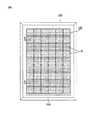
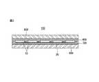
図1は、本発明の一実施の形態に係る太陽電池モジュールの平面を示し、図2は図1のAーA線に沿った断面示す。 FIG. 1 is a plan view of a solar cell module according to an embodiment of the present invention, and FIG. 2 is a cross-sectional view taken along line AA in FIG.
この実施の形態において、太陽電池モジュールは、太陽電池パネル100と、これを支持するフレーム200を含む。 In this embodiment, the solar cell module includes a
フレーム200は、太陽電池パネルの外周を包み込む形で太陽電池パネルに結合されている。このフレーム200は、ステンレスやアルミニウムのような軽い金属材で作られる。 The
太陽電池パネルを構成するアセンブリ210は、複数の太陽電池がマトリックス配列を成しており、これらが電気的に接続されることにより構成される。複数の太陽電池10は、配線材25で互いに接続されて、1列のストリング(string:文字列)を成し、このストリングが複数集まって太陽電池アセンブリとなる。図1においては、太陽電池アセンブリが6列のストリングで構成されことを例示する。 The
太陽電池パネル100は、図2に示すように、前面(入射面)の上部基板800と後面の下部基板900にサンドイッチされており、その間に透明な上部保護膜600と下部保護膜700が位置し、太陽電池アセンブリを封入(encapsulation)している。この実施の形態においては、上部保護膜600と下部保護膜700を分けて説明するが、液状物質を熱処理して保護膜(600、700)を形成することも可能であり、シートの形で存在する上部保護膜600と下部保護膜700をゲル型化させて作ることも可能である。この場合、保護膜(600、700)は、この実施の形態とは異なり、単一層で作られる。保護膜(600、700)は、EVA(ethylene-vinyl acetate copolymer)、EEA(Ethylene-Ethylacrylate Copolymer)、PVB(Poly vinyl butral)、ポリオレフィン(polyolefine)、シリコン、ウレタン、アクリル、エポキシ等の透光性樹脂からなる。 As shown in FIG. 2, the
上部基板800は、透過性絶縁基板で、好ましくは強化ガラスが用いられる。強化ガラスは、鉄成分の含有量が低い低(low)鉄強化ガラス(low iron tempered glass)であることが好ましく、光の散乱効果を高めるために内側の表面は、凹凸面で形成することができる。 The
下部基板900は、太陽電池パネルで湿気や水分が浸透することを防止し、外部環境から太陽電池パネルを保護するために、水分と酸素の浸透を防止する層、化学的腐食を防止する層、絶縁特性を有する層を含む多層の機能層を含むことができ、このような機能層は、単一層で作られることができる。 The
太陽電池10は、配線材25によって隣接したものと電気的に接続されている。 The
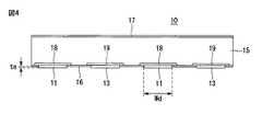
図3は、複数の太陽電池が配線材に接続された図であり、図4は、太陽電池の断面を示す。以下の説明では、構成要素を分けて説明する必要がある場合には、“第1”、“第2”のような序数型表現を用いる。 FIG. 3 is a diagram in which a plurality of solar cells are connected to a wiring member, and FIG. 4 shows a cross section of the solar cells. In the following description, when the components need to be described separately, ordinal expressions such as “first” and “second” are used.
太陽電池10のそれぞれは、薄い厚さを有する立方体形状を有しており、一方の面(例えば、基板の後面)に電子と正孔を分けて収集する第1導電型電極(以下、第1電極) 11と第2導電型電極(以下、第2電極)13が形成されている。 Each of the
第1電極11と第2電極13は、縦方向に長く延長されており、隣接したものと並行するように配列されている。また、第1電極11と第2電極13は、横方向に交互に配列されており、隣接したものと一定の距離を置いて離れている。 The
この第1電極11と第2電極13は、配線材(wiring member)25にそれぞれ電気的に接続されて隣接した他の太陽電池の第2電極13または第1電極11と接続される。 The
配線材25は、電極(11、13)の長さ方向と交差する横方向に配置され、隣接した二つの太陽電池を電気的に接続させる。太陽電池10は、隣接したものと、直列または並列接続することができるが、以下の説明は、直列接続されたことを例として説明する。 The
配線材25は、第1配線材21と第2配線材23を含む。第1配線材21は、中央に配置された第2太陽電池10bの第1電極11に接続されており、他の方は、第3太陽電池10cの第2電極13に接続され、第2太陽電池10bと第3太陽電池10cを直列接続させている。そして、第2配線材23は、中央に配置された第2太陽電池10bの第2電極13に接続されており、他の方は、第1太陽電池10aの第1電極11に接続されて、第2太陽電池10bと、第1太陽電池10aを直列接続させている。 The
この第1配線材21と第2配線材23は、縦方向に交互に配列されており、隣接したものと並行するように配列されている。 The
このように配線材25が電極(11、13)と交差する方向に配置されることにより、配線材25を電極(11、13)に接続することが易しくなり、また、電極(11、13)と配線材25との間のアライン(align)が易しくなる。そして、この実施の形態においては、第1電極11と第2電極13は、すべてが後面に並行するように配列されており、配線材25は、これと交差する方向に接続されることで、配線材25の熱変形方向と電極(11、13)の熱変形方向が交差し、熱変形に起因した潜在的なストレスから太陽電池を保護することができる。 By arranging the
この実施の形態において、配線材25は、電極(11、13)と金属粒子が含まれた樹脂からなる導電層を介して電気的に接続されたり、絶縁性物質からなる絶縁層またはボンディング層を介して絶縁される。 In this embodiment, the
そして、図4に例示するように、この実施の形態において、太陽電池10は、第1電極11と第2電極13の全てが半導体基板15の後面に位置する後面接触型構造をなすもので説明するが、発明がこれに限定するものはない。 As illustrated in FIG. 4, in this embodiment, the
半導体基板15は、pn接合を成しており、半導体基板15の前面(光が入射される面)と後面(前面の反対面)のそれぞれに光の反射防止とパッシベーション(passivation)機能を担当する薄い膜(16、17)が形成されている。 The
そして、第1電極11と、半導体基板15との間、そして第2電極13と、半導体基板15との間には、それぞれエミッタ18と後面電界部19が薄い厚さで形成されて電極(11、13)の方向に電荷が容易に収集することができるように構成されている。第1電極11と第2電極13のそれぞれの幅(Wd)は、薄いエミッタ領域18という水後面電界部19のそれぞれの幅より狭い。第1電極11と第2電極13のそれぞれは、薄い膜16の表面を超えて突出することができる。 And between the
このような太陽電池は、横*縦が160(mm)*160(mm)であり、厚さは250(μm)である。 Such a solar cell has a width * length of 160 (mm) * 160 (mm) and a thickness of 250 (μm).
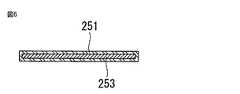
この実施の形態において、配線材25は、図5に例示するような薄い帯状を有するもので説明するが、形状に特に制限があるわけではない。 In this embodiment, the
図5及び図6を見ると、配線材25は、薄い厚さを有する四角帯状を成している。配線材25の断面は長方形の形で、幅(Sd)は、1〜2mmであり、厚さ(Ad)は、60〜120μmである。 5 and 6, the
この実施の形態においては、配線材25の厚さをこのように減少して熱変形を最小化しながら、幅(Sd)を広げ電荷輸送がよくなるように構成している。 In this embodiment, the thickness of the
配線材25は、表面をなすコーティング層251がコア層253を薄い厚さ(15−35(μm))でコーティングした断面を有する。コア層253は、導電性が良いNi、Cu、Ag、Alなどのような金属物質からなり、コーティング層251は、Pb、SnまたはSnIn、SnBi、SnPb、Sn、SnCuAg、SnCuのような化学式を有するはんだからなるか、またはこれらの混合されたもので有り得る。 The
この実施の形態においては、このように構成された10〜36の数の配線材を用いて隣接した二つの太陽電池を電気的に接続している。このような配線材の数はセルの大きさ、配線材の線幅、電極の大きさ、電極のピッチ、電極の形成物質など、さまざまな変数に合わせて、10〜36の内で、その数が決定されることができる。なお、本願の実施例は、その数が10〜36に限定されるものではない。 In this embodiment, two adjacent solar cells are electrically connected using the wiring members of 10 to 36 configured as described above. The number of such wiring materials is 10 to 36 in accordance with various variables such as cell size, wiring material line width, electrode size, electrode pitch, and electrode forming material. Can be determined. In the embodiment of the present application, the number is not limited to 10 to 36.
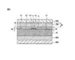
図7は、配線材と電極、そして、ボンディング層の配置図を示し、図8は、図7のB−B線に沿った断面を示す。 FIG. 7 shows a layout of wiring members, electrodes, and bonding layers, and FIG. 8 shows a cross section taken along line BB in FIG.
図面に示すように、この実施の形態において、第1電極11は、一定の線幅を有し1方向に延長されており、第2電極13もまた、一定の線幅を有し、第1電極から所定の距離(Gwa)離れて並行に形成されている(図9参照)。この実施の形態において、第1電極11と第2電極13の線幅Gwは同じであり、280(μm)である。そして、第1電極11と第2電極との間の距離(Gwa)は500(μm)である。 As shown in the drawing, in this embodiment, the
配線材25は、電極(1、13)と交差する方向に延長されており、隣接したものと一定の距離(Wb)で離れて並行するように配列されている。配線材25の線幅(Bw)は、前述したように2(mm)であり、ピッチ(Wb)は6(mm)である。 The
そして、パッド部14が配線材25と電極(11、13)の交点に形成されているが、このパッド部14は、交点で配線材25と電極との間の接触面積を広げ二つの間に容易に接続できるようにし、接触抵抗を低減する。このパッド部14は、横*縦が400(μm)*1.7(mm)の大きさ(Pwb)を有する。このように構成されるパッド部14は、必ずしも必要なわけではない。 And the
図7においては、第2電極13が第1配線材21と接続され、第1電極11が第2配線材23と接続されることを示す。これにより、第1電極の延長方向に、第1電極11が第2配線材23と交差する交点では、第1パッド部141が形成され、第1配線材21と交差する交点では、パッド部が存在しない。第2電極13の場合は、第1電極と反対に第2パッド部143が第2電極13と、第1配線材21が交差する交点でのみ形成されている。 In FIG. 7, the
以下の説明では、電極(11、13)と配線材25が接続される交点を接続点とし、接続されない交点を非接続点とする。この実施の形態のようにパッド部14を含む場合、パッド部14が配置される交点が接続点になり、パッド部14がない交点が非接続点となる。 In the following description, an intersection where the electrodes (11, 13) and the
そして、ボンディング層70が配線材25に沿って形成されている。このボンディング層70は、第1配線材21と第2配線材23のそれぞれに対応してのみ形成されており、接続点に対応するように形成された開口部71を含んでいる。この開口部71を介してパッド部(141、143)が露出される。第1パッド141及び第2パッド143はPwbの幅を持つことができる。 A
ボンディング層70は、配線材25と太陽電池との間に位置して配線材25を太陽電池に付着させる構成で、一例では、このボンディング層70は、保護膜(600、700)と同じEVA(ethylene-vinyl acetate copolymer)、EEA(Ethylene-Ethylacrylate Copolymer)、PVB(Poly vinyl butral)、ポリオレフィン(polyolefine)、シリコン、ウレタン、アクリル、エポキシ等の透光性樹脂からなる。また、このボンディング層70は、高い接着力を得るためにアクリル、エポキシ、紫外線に硬化されるUVレジンのような接着性樹脂からなることもできる。 The
一方、図8に示すように、このような物質からなるボンディング層70上には、下部保護膜700が形成されるが、ボンディング層70の水蒸気透過速度は下部保護膜700の水蒸気透過速度より小さいか等しく、太陽電池を湿気から効果的に保護することができる。 On the other hand, as shown in FIG. 8, the lower
水蒸気透過速度(WVTR、water vapor transmission rate)は、水分の浸透の多少を表す指標として、水蒸気透過速度が高いほど、水蒸気の浸透がよく起こることを意味する。この実施の形態において、ボンディング層70は、下部保護膜700より水分の浸透がよく起こらないか、少なくとも同等の条件であることが望ましい。 The water vapor transmission rate (WVTR) is an index representing the degree of water penetration, and means that the higher the water vapor transmission rate, the more frequently water vapor penetration occurs. In this embodiment, it is desirable that the
ボンディング層70の水蒸気透過速度が後面保護膜700の水蒸気透過速度より小さい場合に、太陽電池の方向に水分が浸透することを効果的に防止することができる。 When the water vapor transmission rate of the
特に、配線材25は、金属物質で水分によって酸化がよく起こる物質で構成されており、酸化が起こる場合、モジュールの性能は落ちることになる。ところが、ボンディング層70は、配線材25に沿って形成されておりながら、これを包み込んでおり、配線材25に水分が浸透することを防止して配線材25が酸化されることを防止する。 In particular, the
ボンディング層70の水蒸気透過速度が下部保護膜700と同じであれば、ボンディング層70と後面保護膜700は、同一の物質で形成することができるので、後面保護膜700とボンディング層70を形成することが易くなる。 If the water vapor transmission rate of the
一方、ボンディング層70の水蒸気透過速度が下部保護膜700より小さい場合、下部保護膜700の形成物質に応じて、ボンディング層70の構成物質もまた選択される。 On the other hand, when the water vapor transmission rate of the
前述したように、この実施の形態において、下部保護膜700は、EVA(ethylene-vinyl acetate copolymer)、EEA(Ethylene-Ethylacrylate Copolymer)、PVB(Poly vinyl butral)、ポリオレフィン(polyolefine)、シリコン、ウレタン、アクリル、エポキシ等の透光性樹脂の内、少なくとも一つを含めて構成される。 As described above, in this embodiment, the lower
一方、ボンディング層70は、アクリル、エポキシ、紫外線に硬化されるUVレジンのような接着性樹脂の内の少なくともいずれか一つを含んでいるが、この内、下部保護膜700と水蒸気透過速度を比較して同じか小さい物質がボンディング層70を成すようになる。このように、この実施の形態において、ボンディング層70は、下部保護膜700に従属してその形成物質が決定される。そして、下部保護膜700の厚さ(Bt)はボンディング層70の厚さ(td)より厚く形成されており、効果的に太陽電池の方向に水分が浸透することを防止することができる。一態様においては、下部保護膜700の厚さ(Bt)は300(μm)〜400(μm)であり、ボンディング層70の厚さ(ed)は70 〜 100(μm)である。この実施の形態において、配線材25は、ボンディング層70によって太陽電池に付着されるので、配線材25に隣接した太陽電池を接続することが易しくなり、配線材25が誤った位置で電極(11、13)と接続されることを防止することができる。 Meanwhile, the
また、開口部71を介してのみ配線材25と接続される電極(11、13)が露出され、非接続点で電極(11、13)は、ボンディング層70に配線材25とブロッキング(blocking)されるので、第1電極11と第2電極13が隣接していてもボンディング層70によって配線材25は、正確に接続しなければならない電極とだけ接続がされる。 In addition, the electrodes (11, 13) connected to the
この実施の形態において、ボンディング層70の幅Btwは、配線材25より広い幅を有し、好ましくは、パッド部14の幅Btwよりも広い線幅を有するが、必ずしも必須ではない。 In this embodiment, the width Btw of the
一方、開口部71を介してはパッド部14が露出され、パッド部14と配線材25との間に導電層41が形成され電極(11、13)と配線材25が接続されたり、パッド部14に配線材25が半田付けされて接続することができる。 On the other hand, the
はんだ付けで配線材25とパッド部14が接続される場合、はんだの溶融温度以上に配線材25を加熱すると、はんだが含んでいる配線材25のコーティング層251が溶けながらパッド部14と溶融結合される。 When the
導電層41は、アクリル、エポキシ、またはUVレジンの内の少なくともいずれか一つを含む接着性樹脂に導電性粒子(conductive particle)が含まれているか、導電性粒子を含むペーストが固体化したものである。導電性粒子としては、Al、Ag、Cuのような導電性金属粒子、またはPb、Sn、SnIn、SnBi、SnPb、Sn、SnCuAgまたはSnCuの内の少なくとも一つを含むはんだで有り得る。 The
開口部71の横*縦の大きさはパッド部14の横*縦より大きく形成され、パッド部14が開口部71を介して完全に露出される大きさを有する。そして、導電層41が開口部71によって露出された空間を埋めるように形成されるが、この時、粘性を有する液状の導電性接着剤が開口部71に塗布されたとき、ボンディング層70が開口部71を除外した残りの部分をマスキング(masking)しており、導電性接着剤により間違ったところで配線材25と電極(11、13)が接続されることを防止することができる。 The horizontal * vertical size of the
このように開口部71を含むボンディング層70の厚さ(td)は、電極(11、13)の厚さ(ed)よりは少なくとも大きい場合、開口部71を除外したところで電極(11、13)と配線材25が誤って接続されることを防止することができる。 When the thickness (td) of the
また、開口部71の大きさを調節してボンディング層70の接着力を向上させ、又は、減少させることができる。開口部71の大きさを減少させるほど、一例として、開口部71の縦方向のサイズ(配線材25の長さ方向)を減らすほどこれに比例してボンディング層70の塗布面積は増え接着力は大きくなり、逆に開口部71の大きさを大きくするほど接着力は減少する。 In addition, the adhesive strength of the
これと反対に、配線材25と電極(11、13)との間の接続力は 開口部71の大きさが大きくなるほど増え、開口部71の大きさが小さくなるほど減少する。 On the contrary, the connection force between the wiring
したがって、接続力を大きくしようとすれば開口部71の大きさを増やし、接着力を大きくするには開口部71の大きさを減少させ、1以上の様々な変数に合わせてボンディング層70を構成することが可能である。 Therefore, if the connection force is increased, the size of the
したがって、開口部71の大きさは、全体が同じであることもあり、選択に応じて、異なるように構成することもできる。 Accordingly, the size of the
このように、この実施の形態においては、ボンディング層70が形成され、電極を太陽電池に固定するので、接続点でのみ配線材が電極と接続して配線材の結合力が低下する問題を解決することができる。 Thus, in this embodiment, since the
また、ボンディング層70の水蒸気透過速度が下部保護膜700よりも、少なくとも同じか小さいので、配線材25が、湿気により酸化されることを防止することができる。 Further, since the water vapor transmission rate of the
一方、以上の説明では、電極(11、13)が非接続点でボンディング層70により、配線材25と接続されないことを説明したが、非接続点に沿って絶縁層43が位置して電極(11、13)と配線材25との間を絶縁させるように構成することもできる。 On the other hand, in the above description, it has been described that the electrodes (11, 13) are not connected to the
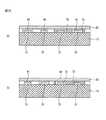
図9は、非接続点に絶縁層43が、さらに形成された図を示し、図10は、図9のC−C線方向に沿った断面図を示す。 FIG. 9 shows a view in which an insulating
この実施の形態において、ボンディング層70は、接続点でパッド部14を露出させる第1開口部711と非接続点で電極(11、13)を露出させる第2開口部713を含む。 In this embodiment, the
第1開口部711は、前述したように、導電層41が位置して電極(11、13)と配線材25を接続させる。 As described above, the
そして、第2開口部713には、絶縁層43が位置し、非接続点で電極(11、13)と配線材25との間を絶縁させている。 The insulating
一方、第1開口部711は、接続点に存在するパッド部14を露出させなければならないが、第2開口部713は、パッドに露出する必要はない。したがって、第2開口部713の横*縦の大きさは、 第1開口部711の大きさに比べて小さいことがありうる。 On the other hand, the
絶縁層43は、絶縁性接着剤が固体化された構成であり、絶縁性接着剤は、エポキシ(epoxy)系またはシリコン系等の合成樹脂、またはセラミックのような絶縁物質からなる。 The insulating
このような絶縁層43は、ボンディング層70を形成した後、導電性接着剤を塗布する際に、絶縁性接着剤と共に塗布がされ、導電性接着剤が熱処理されるとき、絶縁性接着剤と共に熱処理が行われ、それぞれ導電層41と絶縁層43を形成することができる。 Such an insulating
このように、この実施の形態においては、配線材25は、ボンディング層70によって太陽電池に付着され、接続点では導電層41によって電極(11、13)と配線材25が接続され、非接続点では絶縁層43によって電極(11、13)と配線材25が接続されることを防止する。 Thus, in this embodiment, the
以上の説明においては、ボンディング層70が配線材25に対応してのみ形成されるもので説明したが、このボンディング層70は、太陽電池の後面全体に形成されることも可能である。このようにボンディング層70が、基板の後面全体に形成されると、太陽電池を湿気からさらに効果的に保護することができる。 In the above description, the
一般的に、太陽電池モジュールは、太陽電池を挟んで、上部保護膜と下部保護膜、そして、上部基板と下部基板が前面と後面にそれぞれ順次位置して太陽電池を封入(encapsulation)している。 In general, a solar cell module encapsulates a solar cell with an upper protective film and a lower protective film sandwiched between the solar cells, and an upper substrate and a lower substrate positioned sequentially on the front surface and the rear surface, respectively. .
ところで、ボンディング層70を基板の後面全体に形成する場合には、太陽電池10と下部保護膜700との間のボンディング層70が、さらに位置するようになるので、さらにボンディング層70は太陽電池への水蒸気の浸透を効果的に防止することができる。 By the way, when the
この場合に、ボンディング層70は、下部保護膜700と同一の物質で形成することができる。太陽電池モジュールを構成するとき、前述した構成要素を順次積層した状態でラミネートすることになるが、この過程でボンディング層70と下部保護膜700が同一の物質であれば熱融着が起こり、同じ物質間の熱融着により、変色または剥離のような問題を発生させず、また、同じ物質によって効果的に太陽電池10をパッケージングすることができる。 In this case, the
また、効果的に水蒸気を遮断するために、ボンディング層70の水蒸気透過速度は下部保護膜700の水蒸気透過速度より同じか小さい。この場合に、水蒸気透過速度は、太陽電池モジュール内で太陽電池に近づくほど小さくなるので、湿気が保護膜700を、一部透過しても、ボンディング層70で完全に遮断することができる。 Further, in order to effectively block water vapor, the water vapor transmission rate of the
図11は、電極(11、13)が非接続点に沿って断線部を含んで構成された図を示す。 FIG. 11 shows a diagram in which the electrodes (11, 13) are configured to include a disconnection portion along a non-connection point.
この実施の形態において、第1電極11と第2電極13のそれぞれは、非接続点に位置する断線部111を含んで構成される。 In this embodiment, each of the
断線部111は、電極の一部が長さ方向に切れているところ(又は第1電極11及び第2電極13の一部が欠けているところ)に、 非接続点で電極(11、13)と配線材25が物理的に接触することを根本的に防止する。断線部111の幅(Cw)はパッド部14の幅と同じか、それより小さいことがある。 The
このような、断線部111は、第1電極11と、第1配線材21が交差する、非接続点に形成される第1断線部111aと第2電極13と第2配線材23が交差する非接続点 に形成される第2断線部111bを含む。 In such a
電極(11、13)が、このように断線部111を含んでいても、電極(11、13)は、接続点で配線材25と互いに接続されており、効率が低下する問題を発生させない。むしろ、電極(11、13)が断線部111を含むことにより、製造業者の立場では、製造原価を低減することができる。 Even if the electrodes (11, 13) include the
このように、電極(11、13)が断線部111を含む場合、非接続点で電極(11、13)が配線材25と接続されることを未然に遮断することができ、これにより、ボンディング層70に非接続点で電極(11、13)と配線材25が接続されないようにする必要がないので、ボンディング層70の厚さを減少することができる。 Thus, when the electrode (11, 13) includes the
一方、このように電極(11、13)が断線部111を含む場合、ボンディング層70の幅W70は、断線部111の幅Cwより大きくてボンディング層70が断線部111を形成している電極の端111Eを被服するように構成することが望ましい。 On the other hand, when the electrodes (11, 13) include the
電極の端111Eは、熱変形が容易に起こるところで、太陽電池が高温に露出されるとき、熱変形によって容易に剥離する。しかし、このようにボンディング層70が電極の先端をラッピング(wraping)することにより、このような問題を防止することができる。 The
これまで、前述したようなボンディング層70が配線材25と、重畳されるが、配線材25の長さ方向と同じ方向に形成される場合を一例として説明したが、これとは異なるように、ボンディング層70は、配線材25の長さ方向と交差する方向に形成することもある。 So far, the
これに対し、以下の図12〜図15を参照してさらに具体的に説明する。 This will be described more specifically with reference to FIGS. 12 to 15 below.
以下の前述の内容と同じ内容については省略し異なる点を中心に説明する。併せて、図12〜図15は、前述したパッド部と、断線部のない場合を一例として図示しているが、前述のように備えることもある。 The following content that is the same as the content described above will be omitted and will be described mainly. In addition, FIGS. 12 to 15 illustrate the case where the pad portion and the disconnection portion described above are not provided as an example, but may be provided as described above.
図12及び図13は、ボンディング層70の長さ方向が配線材25の長さ方向と交差して形成された第1実施例について説明するための図で、図12は、ボンディング層70の長さ方向が配線材25の長さ方向と交差して形成された平面図を示すものであり、図13の(a)は、図12でD−Dラインに沿った断面を示すものであり、図13の(b)は、図12でE−Eラインに沿った断面を示すものである。 12 and 13 are diagrams for explaining the first embodiment in which the length direction of the
図12に示すように、複数のボンディング層70のそれぞれは、複数の配線材25のそれぞれと交差する方向に長く形成することができる。 As shown in FIG. 12, each of the plurality of bonding layers 70 can be formed long in a direction intersecting with each of the plurality of
したがって、ボンディング層70の長さ方向は、電極(11、13)の長さ方向と同じ方向に長く、複数形成することができる。このようなボンディング層70の材質は、前述したところと同じで有り得る。 Therefore, the length direction of the
これにより、ボンディング層70を複数の配線材25の数だけ備えてなくても、太陽電池モジュールの製造工程の内、配線材25を安定的に半導体基板15の後面に接着されるようにすることができ、製造コストを低減しながら、工程の効率をさらに向上させることができる。 Thus, the
このとき、ボンディング層70の線幅(W70)は、互いに隣接する二つの電極(11、13)との間の距離より大きいことができる。 At this time, the line width (W70) of the
したがって、ボンディング層70の線幅(W70)は、図12に示すように、少なくとも二つの電極(11、13)を覆うことができる幅を有することができる。図12では、ボンディング層70が二つの電極(11、13)を覆う線幅を有する場合を一例として示したが、ボンディング層70は、二つ以上、つまり3〜4個以上の電極(11、13 )を覆う線幅を有することもできる。 Therefore, as shown in FIG. 12, the line width (W70) of the
ボンディング層70が、このような線幅を有するようにすることにより、太陽電池モジュールを製造する工程の間に、配線材25が十分に半導体基板15の後面に接着するように物理的な力を有するようにすることができる。 By making the
このように、図12に示されたボンディング層70は、図13の(a)及び(b)に示すように、配線材25と電極(11、13)との間に位置するので、互いに電気的に接続されるべき配線材25と電極(11、13)との間では、開口部71が備えられることができる。 Thus, the
一例として、図13の(a)及び(b)に示すように、第1配線材21と、第1電極11が接続され、第2配線材23と第2電極13が接続される場合、複数のボンディング層70のそれぞれは、第1配線材21と、第1電極11が互いに交差する地点と第2配線材23と第2電極13が互いに交差する地点に開口部71を備えることができる。 As an example, as shown in FIGS. 13A and 13B, when the
さらに、第1配線材21と、第1電極13は、導電層41によって互いに電気的に接続することができ、第2配線材23と第2電極13は、導電層41によって互いに電気的に接続することができる。 Furthermore, the
また、図13の(a)及び(b)に示すように、第1配線材21と第2電極13は、ボンディング層70によって互いに絶縁されることがあり、第2配線材23と、第1電極13もボンディング層70によって互いに絶縁することができる。 Further, as shown in FIGS. 13A and 13B, the
さらに、ボンディング層70を備えない部分では、別の絶縁層43によって第1配線材21と第2電極13が互いに絶縁され、第2配線材23と第1電極13が互いに絶縁されることができる。 Further, in a portion not provided with the
ここで、導電層41と絶縁層43の材質は、前述したようと同じで有り得る。 Here, the material of the
図12及び図13においては、ボンディング層70の長さ方向が配線材25の長さ方向と交差して形成されるが、ボンディング層70が電極(11、13)と配線材25の間に形成された場合を一例として説明したが、これと異なるようにボンディング層70は、配線材25を覆うように備えることもある。これに対して、さらに具体的に説明すると、次の通りである。 12 and 13, the length direction of the
図14及び図15は、ボンディング層70の長さ方向が配線材25の長さ方向と交差して形成された第2実施例について説明するための図であり、図14は、ボンディング層70の長さ方向が配線材25の長さ方向と交差して、配線材25を被覆するように形成された平面図を示すものであり、図15の(a)は、図14でFーFラインに沿った断面を示すものであり、図15(b)は、図14でG−Gラインに沿った断面を示すものである。 14 and 15 are diagrams for explaining a second embodiment in which the length direction of the
図14及び図15に示すように、ボンディング層70は、配線材25の長さ方向と交差する方向に長く形成されるが、配線材25を覆うように形成することができる。 As shown in FIGS. 14 and 15, the
このようなボンディング層70は、図14に示すように、配線材25と絶縁されるべき電極(11、13)の上に絶縁層43が形成され、配線材25と電気的に接続されるべき電極(11、13)の上に導電層41が形成され、配線材25が電極(11、13)の上に配置された状態で、ボンディング層70が塗布されたり、接着され、配線材25を半導体基板15の後面に固定させることができる。 As shown in FIG. 14, such a
このような配線材25がボンディング層70によって固定された状態で、熱圧着させるラミネート工程中にボンディング層70が溶け配線材25と、半導体基板15との間、または配線材25と電極(11、13)との間の空きスペースを満たした状態で硬化することができる。 In a state where the
さらに、このようなラミネート工程中に導電層41が溶け配線材25と電極(11、13)を互いに電気的に接続させることができる。 Furthermore, the
これにより、図15の(a)及び(b)に示すように、ボンディング層70が形成されることがある。 Thereby, as shown in FIGS. 15A and 15B, the
さらに、図14及び図15においては、半導体基板15の後面領域の中でボンディング層70が形成された領域にも、絶縁層43が別途備えた場合を一例として示したが、これと異なるようにボンディング層70が形成され領域では、ボンディング層70が絶縁機能を実行することができるので、別途の絶縁層43が省略されることもある。 Further, in FIGS. 14 and 15, the case where the insulating
さらに、ボンディング層70の長さ方向が配線材25の長さ方向と交差して形成された第2実施例では、先の第1実施例で説明したようもの異なって、ボンディング層70の開口部71が省略されることがある。 Furthermore, the second embodiment in which the length direction of the
さらに、第2実施例においては、ボンディング層70が配線材25を覆うように備えられ、開口部が省略されるので、図12及び図13と異なって、ボンディング層70を配線材25の上に形成する際に、精巧するアライン工程が必要なく、工程がさらに容易になることができる。 Further, in the second embodiment, since the
Claims (20)
Translated fromJapanese前記複数の太陽電池の内で互いに隣接した複数の太陽電池を前記第1電極と前記第2電極が交差する方向で電気的に接続する複数の配線材と、
前記複数の配線材を前記複数の太陽電池に固定する複数のボンディング層を含む、太陽電池モジュール。A plurality of solar cells each including a first electrode and a second electrode arranged alternately in parallel;
A plurality of wiring members for electrically connecting a plurality of solar cells adjacent to each other among the plurality of solar cells in a direction in which the first electrode and the second electrode intersect;
A solar cell module including a plurality of bonding layers for fixing the plurality of wiring members to the plurality of solar cells.
前記複数のボンディング層は、前記複数の配線材に沿って延長する、請求項1に記載の太陽電池モジュール。The width of the plurality of bonding layers is wider than the width of the wiring material, narrower than the pitch of the plurality of wiring materials,
The solar cell module according to claim 1, wherein the plurality of bonding layers extend along the plurality of wiring members.
前記複数の配線材の幅は1〜2mmであり、前記複数の配線材の厚さは60〜120μmである、請求項1に記載の太陽電池モジュール。The plurality of wiring members have a rectangular cross section,
The solar cell module according to claim 1, wherein the plurality of wiring members have a width of 1 to 2 mm, and the plurality of wiring members have a thickness of 60 to 120 μm.
前記複数の太陽電池の内で互いに隣接した複数の太陽電池を、前記第1電極と前記第2電極が交差する方向で電気的に接続する複数の配線材と、
前記複数の配線材を前記複数の太陽電池に固定する複数のボンディング層であって、それぞれのボンディング層が複数のホールを含むボンディング層を含み、
前記複数のホールは、第1電極の少なくとも一つの部分と第2電極の少なくとも一つの部分のいずれか又は両方に露出する、太陽電池モジュール。A plurality of solar cells each including a first electrode and a second electrode arranged alternately in parallel;
A plurality of wiring members for electrically connecting a plurality of solar cells adjacent to each other among the plurality of solar cells in a direction in which the first electrode and the second electrode intersect;
A plurality of bonding layers for fixing the plurality of wiring members to the plurality of solar cells, each bonding layer including a bonding layer including a plurality of holes;
The plurality of holes are exposed to at least one part of the first electrode and / or at least one part of the second electrode.
Applications Claiming Priority (2)
| Application Number | Priority Date | Filing Date | Title |
|---|---|---|---|
| KR1020140152366AKR102319724B1 (en) | 2014-11-04 | 2014-11-04 | Solar cell |
| KR10-2014-0152366 | 2014-11-04 |
Publications (2)
| Publication Number | Publication Date |
|---|---|
| JP2016092421Atrue JP2016092421A (en) | 2016-05-23 |
| JP6921474B2 JP6921474B2 (en) | 2021-08-18 |
Family
ID=54365934
Family Applications (1)
| Application Number | Title | Priority Date | Filing Date |
|---|---|---|---|
| JP2015215700AActiveJP6921474B2 (en) | 2014-11-04 | 2015-11-02 | Solar cell module |
Country Status (4)
| Country | Link |
|---|---|
| US (1) | US10916671B2 (en) |
| EP (1) | EP3018717B1 (en) |
| JP (1) | JP6921474B2 (en) |
| KR (1) | KR102319724B1 (en) |
Cited By (3)
| Publication number | Priority date | Publication date | Assignee | Title |
|---|---|---|---|---|
| JP2020053487A (en)* | 2018-09-25 | 2020-04-02 | シャープ株式会社 | Solar cell module |
| JP2022011614A (en)* | 2020-06-30 | 2022-01-17 | パナソニック株式会社 | Solar cell module |
| US12183843B1 (en) | 2023-09-05 | 2024-12-31 | Jinko Solar (Haining) Co., Ltd. | Method for manufacturing photovoltaic module and photovoltaic module |
Families Citing this family (4)
| Publication number | Priority date | Publication date | Assignee | Title |
|---|---|---|---|---|
| DE112016006018T5 (en)* | 2015-12-24 | 2018-09-20 | Toyota Jidosha Kabushiki Kaisha | SOLAR BATTERY MODULE |
| WO2019191689A1 (en) | 2018-03-29 | 2019-10-03 | Sunpower Corporation | Wire-based metallization and stringing for solar cells |
| DE102021111786A1 (en) | 2021-05-06 | 2022-11-10 | Hanwha Q Cells Gmbh | Solar panel and use of a protective layer |
| CN118888614B (en)* | 2024-09-09 | 2025-07-18 | 隆基绿能科技股份有限公司 | Back contact cells and photovoltaic modules |
Citations (6)
| Publication number | Priority date | Publication date | Assignee | Title |
|---|---|---|---|---|
| US20080216887A1 (en)* | 2006-12-22 | 2008-09-11 | Advent Solar, Inc. | Interconnect Technologies for Back Contact Solar Cells and Modules |
| JP2011003724A (en)* | 2009-06-18 | 2011-01-06 | Sanyo Electric Co Ltd | Solar cell module |
| JP2011054831A (en)* | 2009-09-03 | 2011-03-17 | Sharp Corp | Back contact type solar cell, solar cell string, and solar cell module |
| WO2013140325A1 (en)* | 2012-03-19 | 2013-09-26 | Renewable Energy Corporation Asa | Cell and module processing of semiconductor wafers for back-contacted solar photovoltaic module |
| JP2014013838A (en)* | 2012-07-04 | 2014-01-23 | Dainippon Printing Co Ltd | Solar battery power collecting sheet and solar battery module |
| JPWO2012043770A1 (en)* | 2010-09-29 | 2014-02-24 | 京セラ株式会社 | Solar cell module and manufacturing method thereof |
Family Cites Families (9)
| Publication number | Priority date | Publication date | Assignee | Title |
|---|---|---|---|---|
| US20070295381A1 (en)* | 2004-03-29 | 2007-12-27 | Kyocera Corporation | Solar Cell Module and Photovoltaic Power Generator Using This |
| US8049099B2 (en)* | 2006-03-01 | 2011-11-01 | Sanyo Electric Co., Ltd. | Solar cell and solar cell module including the same |
| DE102011001061B4 (en)* | 2011-03-03 | 2017-10-05 | Solarworld Innovations Gmbh | Solar cell connector, solar cell module and method of electrically connecting multiple solar cells |
| KR101218416B1 (en)* | 2011-05-25 | 2013-01-21 | 현대중공업 주식회사 | Solar cell module |
| NL2006966C2 (en) | 2011-06-17 | 2012-12-18 | Stichting Energie | Photovoltaic system and connector for a photovoltaic cell with interdigitated contacts. |
| JP5886588B2 (en)* | 2011-10-18 | 2016-03-16 | デクセリアルズ株式会社 | Conductive adhesive, solar cell module using the same, and manufacturing method thereof |
| KR101329222B1 (en)* | 2011-11-22 | 2013-11-14 | 가부시키가이샤 가네카 | Solar cell, manufacturing method thereof, and solar cell module |
| CN103928077B (en)* | 2013-01-10 | 2017-06-06 | 杜邦公司 | Electroconductive binder containing co-blending elastic body |
| CN103337529A (en)* | 2013-07-12 | 2013-10-02 | 苏州润阳光伏科技有限公司 | Electrode of full-back-contact solar cell and fabrication method of electrode |
- 2014
- 2014-11-04KRKR1020140152366Apatent/KR102319724B1/enactiveActive
- 2015
- 2015-11-02JPJP2015215700Apatent/JP6921474B2/enactiveActive
- 2015-11-03USUS14/931,507patent/US10916671B2/enactiveActive
- 2015-11-03EPEP15003143.3Apatent/EP3018717B1/enactiveActive
Patent Citations (6)
| Publication number | Priority date | Publication date | Assignee | Title |
|---|---|---|---|---|
| US20080216887A1 (en)* | 2006-12-22 | 2008-09-11 | Advent Solar, Inc. | Interconnect Technologies for Back Contact Solar Cells and Modules |
| JP2011003724A (en)* | 2009-06-18 | 2011-01-06 | Sanyo Electric Co Ltd | Solar cell module |
| JP2011054831A (en)* | 2009-09-03 | 2011-03-17 | Sharp Corp | Back contact type solar cell, solar cell string, and solar cell module |
| JPWO2012043770A1 (en)* | 2010-09-29 | 2014-02-24 | 京セラ株式会社 | Solar cell module and manufacturing method thereof |
| WO2013140325A1 (en)* | 2012-03-19 | 2013-09-26 | Renewable Energy Corporation Asa | Cell and module processing of semiconductor wafers for back-contacted solar photovoltaic module |
| JP2014013838A (en)* | 2012-07-04 | 2014-01-23 | Dainippon Printing Co Ltd | Solar battery power collecting sheet and solar battery module |
Cited By (6)
| Publication number | Priority date | Publication date | Assignee | Title |
|---|---|---|---|---|
| JP2020053487A (en)* | 2018-09-25 | 2020-04-02 | シャープ株式会社 | Solar cell module |
| JP7203546B2 (en) | 2018-09-25 | 2023-01-13 | シャープ株式会社 | solar module |
| JP2022011614A (en)* | 2020-06-30 | 2022-01-17 | パナソニック株式会社 | Solar cell module |
| JP7481177B2 (en) | 2020-06-30 | 2024-05-10 | パナソニックホールディングス株式会社 | Solar Cell Module |
| US12183843B1 (en) | 2023-09-05 | 2024-12-31 | Jinko Solar (Haining) Co., Ltd. | Method for manufacturing photovoltaic module and photovoltaic module |
| JP2025037216A (en)* | 2023-09-05 | 2025-03-17 | 晶科能源(海▲寧▼)有限公司 | Method for manufacturing a photovoltaic power generation module and a photovoltaic power generation module |
Also Published As
| Publication number | Publication date |
|---|---|
| KR102319724B1 (en) | 2021-11-01 |
| JP6921474B2 (en) | 2021-08-18 |
| EP3018717A1 (en) | 2016-05-11 |
| KR20160052263A (en) | 2016-05-12 |
| US10916671B2 (en) | 2021-02-09 |
| US20160126386A1 (en) | 2016-05-05 |
| EP3018717B1 (en) | 2018-04-25 |
Similar Documents
| Publication | Publication Date | Title |
|---|---|---|
| JP6921474B2 (en) | Solar cell module | |
| JP6307131B2 (en) | Solar cell module and manufacturing method thereof | |
| CN102804393B (en) | Wiring sheet, solar cell with wiring sheet, solar cell module and wiring sheet roll | |
| KR101889842B1 (en) | Solar cell module | |
| JP5651651B2 (en) | Solar cell module | |
| US6133521A (en) | Solar battery output section and its method of manufacture | |
| CN102687281A (en) | Wiring sheet, solar battery cell with wiring sheet, solar battery module, and wiring sheet roll | |
| US10622499B2 (en) | Solar cell module | |
| JP7129786B2 (en) | SOLAR CELL WITH IMPROVED STRUCTURE AND SOLAR CELL MODULE USING THE SAME | |
| US20160181454A1 (en) | Solar cell module and method for manufacturing the same | |
| WO2018116643A1 (en) | Solar cell module and method for manufacturing solar cell module | |
| KR102298447B1 (en) | Solar cell module | |
| JPWO2018142544A1 (en) | Solar cell module and method of manufacturing the same | |
| CN111727485A (en) | Wiring and solar cell and solar cell module using the wiring | |
| KR101788160B1 (en) | Solar cell module | |
| KR101788169B1 (en) | Solar cell module and solar cell | |
| KR102298434B1 (en) | Solar cell module and manufacturing method thereof | |
| KR102233889B1 (en) | Solar cell module and manufacturing method thereof | |
| KR101823601B1 (en) | Solar cell module | |
| KR20180104505A (en) | solar cell and solar cell module | |
| KR101816180B1 (en) | Solar cell module | |
| KR20180105837A (en) | Solar cell module and manufacturing method thereof | |
| JP2024545910A (en) | Electrode Assembly | |
| JP2024503612A (en) | electrode assembly | |
| KR102455605B1 (en) | Solar cell |
Legal Events
| Date | Code | Title | Description |
|---|---|---|---|
| A621 | Written request for application examination | Free format text:JAPANESE INTERMEDIATE CODE: A621 Effective date:20170925 | |
| A977 | Report on retrieval | Free format text:JAPANESE INTERMEDIATE CODE: A971007 Effective date:20180731 | |
| A131 | Notification of reasons for refusal | Free format text:JAPANESE INTERMEDIATE CODE: A131 Effective date:20180821 | |
| A521 | Request for written amendment filed | Free format text:JAPANESE INTERMEDIATE CODE: A523 Effective date:20181121 | |
| A131 | Notification of reasons for refusal | Free format text:JAPANESE INTERMEDIATE CODE: A131 Effective date:20190416 | |
| A601 | Written request for extension of time | Free format text:JAPANESE INTERMEDIATE CODE: A601 Effective date:20190716 | |
| A521 | Request for written amendment filed | Free format text:JAPANESE INTERMEDIATE CODE: A523 Effective date:20190731 | |
| A02 | Decision of refusal | Free format text:JAPANESE INTERMEDIATE CODE: A02 Effective date:20200107 | |
| A521 | Request for written amendment filed | Free format text:JAPANESE INTERMEDIATE CODE: A523 Effective date:20200501 | |
| C60 | Trial request (containing other claim documents, opposition documents) | Free format text:JAPANESE INTERMEDIATE CODE: C60 Effective date:20200501 | |
| A911 | Transfer to examiner for re-examination before appeal (zenchi) | Free format text:JAPANESE INTERMEDIATE CODE: A911 Effective date:20200602 | |
| C21 | Notice of transfer of a case for reconsideration by examiners before appeal proceedings | Free format text:JAPANESE INTERMEDIATE CODE: C21 Effective date:20200609 | |
| A912 | Re-examination (zenchi) completed and case transferred to appeal board | Free format text:JAPANESE INTERMEDIATE CODE: A912 Effective date:20200904 | |
| C211 | Notice of termination of reconsideration by examiners before appeal proceedings | Free format text:JAPANESE INTERMEDIATE CODE: C211 Effective date:20200908 | |
| C22 | Notice of designation (change) of administrative judge | Free format text:JAPANESE INTERMEDIATE CODE: C22 Effective date:20201013 | |
| C13 | Notice of reasons for refusal | Free format text:JAPANESE INTERMEDIATE CODE: C13 Effective date:20201208 | |
| A521 | Request for written amendment filed | Free format text:JAPANESE INTERMEDIATE CODE: A523 Effective date:20210217 | |
| C302 | Record of communication | Free format text:JAPANESE INTERMEDIATE CODE: C302 Effective date:20210423 | |
| C13 | Notice of reasons for refusal | Free format text:JAPANESE INTERMEDIATE CODE: C13 Effective date:20210511 | |
| A521 | Request for written amendment filed | Free format text:JAPANESE INTERMEDIATE CODE: A523 Effective date:20210520 | |
| C23 | Notice of termination of proceedings | Free format text:JAPANESE INTERMEDIATE CODE: C23 Effective date:20210608 | |
| C03 | Trial/appeal decision taken | Free format text:JAPANESE INTERMEDIATE CODE: C03 Effective date:20210706 | |
| C30A | Notification sent | Free format text:JAPANESE INTERMEDIATE CODE: C3012 Effective date:20210706 | |
| A61 | First payment of annual fees (during grant procedure) | Free format text:JAPANESE INTERMEDIATE CODE: A61 Effective date:20210728 | |
| R150 | Certificate of patent or registration of utility model | Ref document number:6921474 Country of ref document:JP Free format text:JAPANESE INTERMEDIATE CODE: R150 | |
| S111 | Request for change of ownership or part of ownership | Free format text:JAPANESE INTERMEDIATE CODE: R313113 | |
| R350 | Written notification of registration of transfer | Free format text:JAPANESE INTERMEDIATE CODE: R350 | |
| S533 | Written request for registration of change of name | Free format text:JAPANESE INTERMEDIATE CODE: R313533 | |
| R350 | Written notification of registration of transfer | Free format text:JAPANESE INTERMEDIATE CODE: R350 | |
| R250 | Receipt of annual fees | Free format text:JAPANESE INTERMEDIATE CODE: R250 | |
| S111 | Request for change of ownership or part of ownership | Free format text:JAPANESE INTERMEDIATE CODE: R313113 | |
| R350 | Written notification of registration of transfer | Free format text:JAPANESE INTERMEDIATE CODE: R350 | |
| R250 | Receipt of annual fees | Free format text:JAPANESE INTERMEDIATE CODE: R250 |