JP2016058790A - Array antenna and device using the same - Google Patents
Array antenna and device using the sameDownload PDFInfo
- Publication number
- JP2016058790A JP2016058790AJP2014181569AJP2014181569AJP2016058790AJP 2016058790 AJP2016058790 AJP 2016058790AJP 2014181569 AJP2014181569 AJP 2014181569AJP 2014181569 AJP2014181569 AJP 2014181569AJP 2016058790 AJP2016058790 AJP 2016058790A
- Authority
- JP
- Japan
- Prior art keywords
- array antenna
- slot
- antennas
- waveguide
- waveguides
- Prior art date
- Legal status (The legal status is an assumption and is not a legal conclusion. Google has not performed a legal analysis and makes no representation as to the accuracy of the status listed.)
- Pending
Links
Images


Classifications
- H—ELECTRICITY
- H01—ELECTRIC ELEMENTS
- H01Q—ANTENNAS, i.e. RADIO AERIALS
- H01Q13/00—Waveguide horns or mouths; Slot antennas; Leaky-waveguide antennas; Equivalent structures causing radiation along the transmission path of a guided wave
- H01Q13/20—Non-resonant leaky-waveguide or transmission-line antennas; Equivalent structures causing radiation along the transmission path of a guided wave
- H—ELECTRICITY
- H01—ELECTRIC ELEMENTS
- H01Q—ANTENNAS, i.e. RADIO AERIALS
- H01Q13/00—Waveguide horns or mouths; Slot antennas; Leaky-waveguide antennas; Equivalent structures causing radiation along the transmission path of a guided wave
- H01Q13/10—Resonant slot antennas
- H—ELECTRICITY
- H01—ELECTRIC ELEMENTS
- H01Q—ANTENNAS, i.e. RADIO AERIALS
- H01Q1/00—Details of, or arrangements associated with, antennas
- H01Q1/12—Supports; Mounting means
- H01Q1/22—Supports; Mounting means by structural association with other equipment or articles
- H01Q1/24—Supports; Mounting means by structural association with other equipment or articles with receiving set
- H—ELECTRICITY
- H01—ELECTRIC ELEMENTS
- H01Q—ANTENNAS, i.e. RADIO AERIALS
- H01Q1/00—Details of, or arrangements associated with, antennas
- H01Q1/50—Structural association of antennas with earthing switches, lead-in devices or lightning protectors
- H—ELECTRICITY
- H01—ELECTRIC ELEMENTS
- H01Q—ANTENNAS, i.e. RADIO AERIALS
- H01Q21/00—Antenna arrays or systems
- H01Q21/0006—Particular feeding systems
- H01Q21/0037—Particular feeding systems linear waveguide fed arrays
- H01Q21/0043—Slotted waveguides
- H01Q21/005—Slotted waveguides arrays
- H—ELECTRICITY
- H01—ELECTRIC ELEMENTS
- H01Q—ANTENNAS, i.e. RADIO AERIALS
- H01Q21/00—Antenna arrays or systems
- H01Q21/06—Arrays of individually energised antenna units similarly polarised and spaced apart
- H01Q21/20—Arrays of individually energised antenna units similarly polarised and spaced apart the units being spaced along or adjacent to a curvilinear path
Landscapes
- Variable-Direction Aerials And Aerial Arrays (AREA)
- Waveguide Aerials (AREA)
- Radar Systems Or Details Thereof (AREA)
Abstract
Description
Translated fromJapanese本開示は、例えばコンフォーマル導波管スロットアレーアンテナ装置などのアレーアンテナ装置およびそれを用いた無線通信装置に関する。 The present disclosure relates to an array antenna device such as a conformal waveguide slot array antenna device and a wireless communication device using the same.
例えば特許文献1において、コンフォーマルアンテナの一例が開示されている。当該コンフォーマルアンテナは、「所望の曲面を有するアンテナ基体と、この基体の外まわりに所定のピッチで取り付けられたマイクロストリップアンテナと、アンテナ基体の内側または外側に位置し上記マイクロストリップアンテナに電波を給電する給電回路とから成るアンテナ装置において、マイクロストリップアンテナを構成する誘電体基板、複数個のコネクタと放射導体素子のうち、放射導体素子の厚みを変化させ、その外側の面がアンテナ基体の曲面の一部を成すこと」を特徴としている。なお、コンフォーマルアンテナとは、航空機の胴体のような曲率のある面上に放射素子を配列したアレーアンテナを、一般にコンフォーマルアンテナと呼んでいる。 For example, Patent Document 1 discloses an example of a conformal antenna. The conformal antenna is “an antenna base having a desired curved surface, a microstrip antenna attached at a predetermined pitch around the outside of the base, and a radio wave feeding to the microstrip antenna located inside or outside the antenna base. In the antenna device comprising the power feeding circuit, the thickness of the radiation conductor element among the dielectric substrate constituting the microstrip antenna, the plurality of connectors and the radiation conductor element is changed, and the outer surface is the curved surface of the antenna substrate. It is characterized by "part of it". Note that a conformal antenna generally refers to an array antenna in which radiating elements are arranged on a curved surface such as an aircraft fuselage as a conformal antenna.
また、特許文献2では、例えば三角錐や球の表面、あるいは航空機の胴体のような曲面に放射素子を配列したコンフォーマルアレーアンテナに導波管スロットアンテナを用いた実施例が開示されている。ここで、1つの導波管に複数のスロットを形成することによりコンフォーマル導波管スロットアレーアンテナ装置を構成しており、1つの導波管の上部金属板及び下部金属板が円弧状に形成されている。 Patent Document 2 discloses an embodiment in which a waveguide slot antenna is used as a conformal array antenna in which radiating elements are arranged on a curved surface such as a triangular pyramid, a sphere, or an aircraft fuselage. Here, a conformal waveguide slot array antenna device is formed by forming a plurality of slots in one waveguide, and an upper metal plate and a lower metal plate of one waveguide are formed in an arc shape. Has been.
さらに、特許文献3及び4では、矩形導波管の広壁上に電波の伝搬方向に沿って複数のクロススロットが形成される漏れ波導波管クロススロットアレーアンテナが開示されている。 Further, Patent Documents 3 and 4 disclose a leaky wave waveguide cross slot array antenna in which a plurality of cross slots are formed along the propagation direction of a radio wave on a wide wall of a rectangular waveguide.
例えば特許文献1において開示されたコンフォーマルアンテナでは、基板上に形成された平面アンテナで構成しているので、製造プロセスは簡単であるが、特許文献2〜4で開示された導波管アレーアンテナに比較して低損失化のためには高価な誘電体材料を用いる必要があり、放射角度を広げることは難しいという問題点があった。 For example, the conformal antenna disclosed in Patent Document 1 is composed of a planar antenna formed on a substrate, so that the manufacturing process is simple, but the waveguide array antenna disclosed in Patent Documents 2 to 4 is used. Compared to the above, it is necessary to use an expensive dielectric material for reducing the loss, and there is a problem that it is difficult to widen the radiation angle.
本開示の目的は以上の問題点を解決し、平面アンテナで構成されたコンフォーマルアンテナに比較して低損失で電波を放射でき、しかも放射角度を広げることができ、容易に製造することができるアレーアンテナ装置を提供することにある。 The object of the present disclosure is to solve the above-described problems, and to radiate radio waves with low loss compared to a conformal antenna configured with a planar antenna, and further, to widen a radiation angle and to be easily manufactured. The object is to provide an array antenna device.
本開示に係るアレーアンテナ装置は、
複数のスロットアンテナをそれぞれ含み、コンフォーマル形状で形成された放射面をそれぞれ有する、配列された複数のスロットアレーアンテナと、
上記各スロットアレーアンテナに対してそれぞれ給電するための複数の導波管とを備えたことを特徴とする。An array antenna device according to the present disclosure is:
A plurality of arrayed slot array antennas each including a plurality of slot antennas, each having a radiation surface formed in a conformal shape;
And a plurality of waveguides for supplying power to each of the slot array antennas.
これらの概括的かつ特定の態様は、システム、装置及び方法の任意の組み合わせにより実現してもよい。 These general and specific aspects may be realized by any combination of systems, apparatuses and methods.
本開示に係るアレーアンテナ装置によれば、平面アンテナで構成されたコンフォーマルアンテナに比較して低損失で電波を放射でき、しかも放射角度を広げることができる。 According to the array antenna device according to the present disclosure, it is possible to radiate radio waves with low loss as compared with a conformal antenna configured with a planar antenna, and to widen the radiation angle.
以下、本開示に係る実施形態について図面を参照して説明する。なお、以下の各実施形態において、同様の構成要素については同一の符号を付している。 Embodiments according to the present disclosure will be described below with reference to the drawings. In addition, in each following embodiment, the same code | symbol is attached | subjected about the same component.
実施形態1.
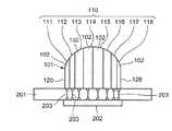
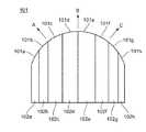
図1は実施形態1に係るコンフォーマル導波管スロットアレーアンテナ装置101の外観を示す斜視図である。図1において、本実施形態に係るコンフォーマル導波管スロットアレーアンテナ装置101は、例えば航空機の胴体のような曲率のあるコンフォーマル形状の放射面110の各狭壁面111〜118上にそれぞれ、複数のスロットアンテナ103をそれぞれ備える複数のスロットアレーアンテナを配列したことを特徴としている。ここで、放射面110は、例えば複数の矩形平板形状の狭壁面111〜118で構成される。放射面110の下部は、側部広壁面120,128の間において側壁104で分離された複数の矩形導波管102で構成される。当該各矩形導波管102に無線信号を給電して同導波管102内を伝搬させた後、複数のスロットアンテナ103からなるスロットアレーアンテナから放射する。Embodiment 1. FIG.
FIG. 1 is a perspective view showing an appearance of a conformal waveguide slot
なお、図1のスロットアンテナ103の形成方向については、図4及び図5を参照して詳細後述する。 1 will be described in detail later with reference to FIGS. 4 and 5. FIG.
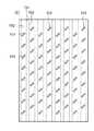
図2は図1のコンフォーマル導波管スロットアレーアンテナ装置101及びその周辺回路の構成を示す側面図である。図2において、コンフォーマル導波管スロットアレーアンテナ装置101の各導波管102の下部の給電部から、コンフォーマル導波管スロットアレーアンテナ装置101の下部に載置された基板201内の給電線203を介して、無線送受信回路を含む集積回路(IC)202に接続される。集積回路202からの無線信号は複数の給電線203及び複数の導波管102を介して放射面110に設けられた複数のアンテナから放射される一方、放射面110で受信される無線信号は複数の導波管102及び複数の給電線203を介して集積回路202に出力される。 FIG. 2 is a side view showing the configuration of the conformal waveguide slot
図3は第1の変形例に係るコンフォーマル導波管スロットアレーアンテナ装置の縦断面図である。第1の変形例に係るコンフォーマル導波管スロットアレーアンテナ装置は、放射面110を各導波管102の狭壁面に対向する狭壁面111〜118のうち隣接する各対の狭壁面をそれぞれ接続面121〜127で連結したことを特徴としている。ここで、狭壁面111は接続面121を介して狭壁面112に連結され、狭壁面112は接続面122を介して狭壁面113に連結され、狭壁面113は接続面123を介して狭壁面114に連結される。狭壁面114は接続面124を介して狭壁面115に連結され、狭壁面115は接続面125を介して狭壁面116に連結され、狭壁面116は接続面126を介して狭壁面117に連結され、狭壁面117は接続面127を介して狭壁面118に連結される。 FIG. 3 is a longitudinal sectional view of a conformal waveguide slot array antenna device according to a first modification. In the conformal waveguide slot array antenna device according to the first modification, the
図3において、放射面110の各狭壁面111〜118と各導波管102との間には無線信号を伝搬させる給電部105が設けられ、各導波管102の下部と各給電線203との間には無線信号を伝搬させる給電部106が設けられる。また、集積回路202の各接続端子204はそれぞれ給電線203に接続される。なお、複数の導波管102はそれぞれ側壁104で分離されている。集積回路202からの無線信号は複数の接続端子204、複数の給電線203、複数の給電部106、複数の導波管102及び給電部105を介して放射面110に設けられた複数のスロットアンテナから放射される。一方、放射面110に設けられた複数のスロットアンテナで受信される無線信号は複数の給電部105、複数の導波管102、複数の給電部106、複数の給電線203、及び複数の接続端子204を介して集積回路202に出力される。 In FIG. 3, a
図3のコンフォーマル導波管スロットアレーアンテナ装置では、各導波管102の狭壁面に対向する狭壁面111〜118にスロットアレーアンテナ装置を形成し、ここで、コンフォーマル形状の放射面110を形成するようにそれぞれ狭壁面111〜118を有する複数の細長い平板を側面で連結して構成した。これにより、図10を参照して詳細後述するように、従来例の平面アンテナに比較して広角化できる。 In the conformal waveguide slot array antenna device of FIG. 3, the slot array antenna device is formed on the narrow wall surfaces 111 to 118 facing the narrow wall surface of each
図4は第2の変形例に係るコンフォーマル導波管スロットアレーアンテナ装置101の平面展開図である。第2の変形例に係るコンフォーマル導波管スロットアレーアンテナ装置101は、放射面110の各狭壁面に形成される複数のスロットアンテナ103が互いに平行であって、狭壁面の長手方向に対して概略45度の角度をなすように形成されている。これにより、図4のコンフォーマル導波管スロットアレーアンテナ装置は、水平偏波と垂直偏波の間の角度を有する直線偏波の偏波面を有する。なお、各隣接するスロットアンテナ103は互いに1波長だけ離隔し、各スロットアンテナ103は半波長の長手方向の長さを有するように形成されている。 FIG. 4 is a developed plan view of a conformal waveguide slot
図5は第3の変形例に係るコンフォーマル導波管スロットアレーアンテナ装置の平面展開図である。図5においては、第3の変形例に係るコンフォーマル導波管スロットアレーアンテナ装置は、狭壁面の長手方向と平行となる長手方向を有する複数のスロットアンテナ103であって、電界Eの矢印で図示するように、スロットアンテナ103のスロットの配置を隣接するブランチのスロットアレーアンテナと互いに逆相となるようにスロットアンテナ103を形成したことを特徴としている。なお、各スロットアレーアンテナにおいて互いに長手方向で隣接するスロットアンテナ103は互いに電界Eの回転方向が逆となるように互いに所定の距離だけ離隔されかつ、狭壁面の短辺方向で右端部又は左端部で互い違いで形成される。これにより、互いに隣接するブランチ(スロットアレーアンテナ)間の電位差が側壁104の中央部でゼロになるために、放射面110の各狭壁面と導波管102とを厳密に対向するように連結しなくても垂直偏波(直線偏波)で動作可能である。このため、放射面110と導波管102を別部品として構成した場合に、放射面110と導波管102を組み立てる場合に厳密に接続する必要がなくなるため、製造プロセスが簡易化され、量産性が増すという効果を生じせしめる。 FIG. 5 is a developed plan view of a conformal waveguide slot array antenna device according to a third modification. In FIG. 5, the conformal waveguide slot array antenna device according to the third modification is a plurality of
なお、図4及び図5は、図1のコンフォーマル導波管スロットアレーアンテナ装置101の平面をそのまま見た平面図ではなく、各スロットアレーアンテナの幅が同一になるようにした平面展開図である。 4 and 5 are not plan views of the conformal waveguide slot
図6は図1のコンフォーマル導波管スロットアレーアンテナ装置の底面の給電部106を示す底面図である。図6に示すように、各導波管102の長手方向の中央部に矩形柱形状の給電部106が形成されている。 FIG. 6 is a bottom view showing the
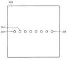
図7は図2及び図3の集積回路(IC)202の上面を示す平面図である。図7に示すように、集積回路202の上部には、複数の接続端子204が形成されている。 FIG. 7 is a plan view showing the top surface of the integrated circuit (IC) 202 of FIGS. As shown in FIG. 7, a plurality of
図8は図1のコンフォーマル導波管スロットアレーアンテナ装置の放射パターン131及び比較例の導波管スロットアレーアンテナ装置の放射パターン132を示す図である。図8において、130は放射基準点であり、実施形態1に係るコンフォーマル導波管スロットアレーアンテナ装置の放射パターンは、比較例に係る導波管スロットアレーアンテナ装置の放射パターン132に比較して広い角度(広角)で放射することができる。 FIG. 8 is a diagram showing a
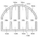
図9は図1のコンフォーマル導波管スロットアレーアンテナ装置101を樹脂成形法で製造する場合の構成を示す縦断面図である。 FIG. 9 is a longitudinal sectional view showing a configuration when the conformal waveguide slot
図9において、図1のコンフォーマル導波管スロットアレーアンテナ装置101を、アンテナ上部101Aと、アンテナ下部101Bとに励振時の電流がおおむねゼロとなる高さの分割位置において導波管の長手方向で2分割する。ここで、導波管102aを上部導波管102aaと下部導波管102abとに2分割し、導波管102aを上部導波管102aaと下部導波管102abとに2分割し、導波管102bを上部導波管102baと下部導波管102bbとに2分割し、導波管102cを上部導波管102caと下部導波管102cbとに2分割し、導波管102dを上部導波管102daと下部導波管102dbとに2分割する。なお、各上部導波管102aa〜102da及び各下部導波管102ab〜102dbでそれぞれ、分割位置から導波管内部を介して導波管端部に向かってその短辺幅が狭くなるように形成することで樹脂成形法でアンテナ上部101A及びアンテナ下部101Bを形成してこれらを貼り付けた後、導波管内部をCuメッキなどの金属メッキで内面を金属薄膜の内面処理を行うことで、導波管102a〜102dを形成することができる。 In FIG. 9, the longitudinal direction of the waveguide of the conformal waveguide slot
なお、樹脂成形法では、導波管本体を例えばエポキシ樹脂や液晶ポリマーなどの樹脂で例えば金属金型を用いて形成し、形成した導波管内面をメッキで表面処理する。ここで、導波管本体は3Dプリンタで形成してもよい。 In the resin molding method, the waveguide body is formed of a resin such as an epoxy resin or a liquid crystal polymer using, for example, a metal mold, and the formed waveguide inner surface is subjected to surface treatment by plating. Here, the waveguide body may be formed by a 3D printer.
以上説明したように、樹脂成形法及びメッキ法を用いて導波管を形成することにより、従来例のように金属を折り曲げなどして導波管を形成する場合に比較して製造プロセスを簡単化でき製造コストを大幅に低減できる。また、導波管で給電するので、無線信号を低損失で伝送することができる。さらに、上述のように、放射面110をコンフォーマル形状とすることで、図8を用いて説明したように広角化できる。 As described above, forming a waveguide using a resin molding method and a plating method simplifies the manufacturing process compared to the case of forming a waveguide by bending metal as in the conventional example. Manufacturing costs can be greatly reduced. In addition, since power is supplied through the waveguide, a radio signal can be transmitted with low loss. Furthermore, as described above, by forming the
図10は図1のコンフォーマル導波管スロットアレーアンテナ装置101の素子間隔を説明するための側面図である。以下、コンフォーマル導波管スロットアレーアンテナ装置101では、コンフォーマルではない導波管スロットアレーアンテナ装置に比較して素子間隔を大きくできる理由について以下に説明する。 FIG. 10 is a side view for explaining the element spacing of the conformal waveguide slot
アレーアンテナでは、一般的に素子間隔を広げるとグレーティングローブが発生しやすくなるため、平面上に等間隔でアンテナ素子を配列する従来構成の場合には、グレーティングローブの発生を抑圧した上でビーム指向方向を広範囲にスキャンする場合には素子間隔を小さくする必要があった。 In array antennas, grating lobes generally tend to occur when the element spacing is increased. Therefore, in the conventional configuration in which antenna elements are arranged at equal intervals on a plane, the beam pointing is performed after suppressing the generation of grating lobes. When scanning the direction in a wide range, it is necessary to reduce the element interval.
一方、本実施形態に係るコンフォーマル導波管スロットアレーアンテナ装置の場合には、アンテナ面がビーム指向方向に対して物理的に傾いて構成されるため、複数のビーム基準方向を設けることが可能となり、各ビーム基準方向に対するアンテナ素子のビームスキャン範囲を狭くすることが可能となる。 On the other hand, in the case of the conformal waveguide slot array antenna device according to the present embodiment, the antenna surface is physically inclined with respect to the beam directing direction, so that a plurality of beam reference directions can be provided. Thus, the beam scan range of the antenna element with respect to each beam reference direction can be narrowed.
具体的には、図10に示す8ブランチ構成の場合に120°の範囲をカバーするためには、ビーム指向方向A、B、Cのそれぞれに対して40°の範囲をカバーすればよく、この場合、ビーム基準方向Aについては、スロットアレーアンテナ101a,101b,101c,101dを主に動作させてビーム指向方向Aを中心とする±20度の範囲をカバーする。同様に、ビーム基準方向Bについては、スロットアレーアンテナ101c,101d,101e,101fを主に動作させてビーム指向方向Bを中心とする±20度の範囲をカバーする。また、ビーム基準方向Cについては、スロットアレーアンテナ101e,101f,101g,101hを主に動作させてビーム指向方向Cを中心とする±20度の範囲をカバーする。これにより、各ビーム基準方向A,B,Cに対するビームスキャン範囲を狭くすることが可能となるため、アンテナ素子間隔を広くしてもグレーティングローブが生じることなく、利得が高い上に半値角の狭い良好なビーム指向性を形成することが可能となる。 Specifically, in the case of the 8-branch configuration shown in FIG. 10, in order to cover the range of 120 °, it is sufficient to cover the range of 40 ° with respect to each of the beam directing directions A, B, and C. In this case, with respect to the beam reference direction A, the
なお、ビーム基準方向とは、アレーアンテナ全体のうち少なくとも2つ以上のアンテナ素子で構成されるサブアレーに対する概正面方向のことであり、本実施形態では、ビーム基準方向が3つの場合について説明したが、これに限定されるものではなく、例えば、4つ以上のビーム基準方向を備えていても良いことは当然のことである。すなわち、本開示では、放射面110において互いに異なる3つ以上のビーム基準方向を備えて、各ビーム基準方向に対して4つ以上のスロットアレーアンテナを割り当てて所定のビーム指向性を得ることができる。 The beam reference direction is a general front direction with respect to a subarray including at least two antenna elements of the entire array antenna. In the present embodiment, the case where there are three beam reference directions has been described. However, the present invention is not limited to this. For example, it is a matter of course that four or more beam reference directions may be provided. That is, according to the present disclosure, it is possible to obtain three or more beam reference directions different from each other on the
なお、平面上に等間隔で配置された従来のアレーアンテナの場合には、ビーム基準方向は正面方向のみとなることは自明である。 In the case of a conventional array antenna arranged at equal intervals on a plane, it is obvious that the beam reference direction is only the front direction.
なお、ビーム基準方向と反対方向となる一部のサブアレーを非励振とすることで、装置全体の消費電力を抑えることが期待できることは当然のことである。この場合、例えば、ビーム基準方向Aに対してはスロットアレーアンテナ101a、101b、101c、101d、101eを励振しつつ、スロットアレーアンテナ101f、101g、101hを非励振とすることですべてのスロットアレーアンテナを励振する場合に比べて消費電力を少なくすることが可能となる。非励振とするスロットアレーアンテナはこれに限定されるものではない。 Of course, it can be expected that the power consumption of the entire apparatus can be suppressed by de-exciting some of the subarrays in the direction opposite to the beam reference direction. In this case, for example, with respect to the beam reference direction A, all the
図11は図1のコンフォーマル導波管スロットアレーアンテナ装置の各導波管において管内波長を揃えることを説明するための側面図である。図11において、導波管102a,102bが側壁104aで分離され、導波管102c,102dが側壁104bで分離されている。 FIG. 11 is a side view for explaining that the waveguide wavelengths are aligned in each waveguide of the conformal waveguide slot array antenna device of FIG. In FIG. 11,
導波管102a〜102dを形成する側壁104a,104bを、各導波管102a〜102dが平行となるように構成する場合には、中心付近の壁の長さに比べて端部付近の壁の長さが短くなるため、管内波長が著しく異なってしまい、広い周波数をカバーすることができないという課題があった。 When the
一般的に導波管の管内波長λcは、導波管の長手方向の長さをaとすると式(1)で表される。この場合、λ0は自由空間波長である。また、λ0=2aとなる場合に数式1は発散してしまうため、a>λ0/2であることが必要となり、さらに、a>λ0となると高次モードが発生することから、長手方向の長さaは式(2)に示される範囲内で設計することが重要となる。一方、狭壁面にアンテナ素子を形成する場合には、短手方向の長さbは高次モードを抑制するためには、式(3)のごとくλ0/2より短く設計する必要がある。In general, the in-tube wavelength λc of the waveguide is expressed by Expression (1), where a is the length in the longitudinal direction of the waveguide. In this case, λ0 is the free space wavelength. Further, since the equation 1 when the lambda0 = 2a is diverges, it is necessary a a> λ0/2, Further, since the high-order mode is generated when the a> lambda0, the longitudinal It is important that the length a in the direction is designed within the range shown in the equation (2). On the other hand, in the case of forming the antenna element on the narrow wall, the length b in the lateral direction in order to suppress higher modes, it is necessary to design shorter than lambda0/2 as the equation (3).

そこで、図11に示すように、一部もしくはすべての側壁104を給電面に対して垂直とならないように形成することにより、端部付近の壁の長さを長くすることが可能となるため、管内波長を略均一にすることができるため、広い周波数をカバーすることが可能となることが期待できる。この場合、中心付近の壁の長さはa1であるのに対して、端部の導波管の壁の長さはa2となっている。長さa2は長さa1よりは短いものの、アンテナ面の高さa3より長くすることができ、結果的に管内波長λcが長くなることを抑制する効果が期待できる。Therefore, as shown in FIG. 11, by forming part or all of the
なお、端部の導波管の管内波長を従来に比べて長くすることができさえすれば、図11に示した壁の形状に限定されるものではなく、例えば、図9に示すように、上下2つの部品として構成する場合には壁の根元の幅を解放部の幅よりも太くなるようにすることで、長さbがλ0/2以下となるよう抑制しつつ、長さaを長くできるため、同様の効果が期待できることはいうまでもない。As long as the in-tube wavelength of the end waveguide can be made longer than the conventional one, it is not limited to the shape of the wall shown in FIG. 11, for example, as shown in FIG. up and down when configured as two parts by the so thicker than the width of the releasing portion the width of the base of the wall, while suppressing that the length b is lambda0/2 or less, the length a Needless to say, the same effect can be expected because it can be made longer.
実施形態2.
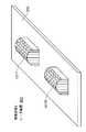
図12は実施形態2に係るレーダ装置300の外観を示す斜視図である。実施形態2に係るレーダ装置300は、図12に示すように、実施形態1に係る2個のコンフォーマル導波管スロットアレーアンテナ装置101を送信アンテナ101T及び受信アンテナ101Rとして用いて構成したことを特徴としている。図12において、基板310上に送信アンテナ101T及び受信アンテナ101Rが並置され、それらの基板下部に図13の無線送信回路321及び図14の無線受信回路322を備えてレーダ装置300のためのRFモジュールを構成する。当該レーダ装置300は例えば車両の衝突防止のための車両検出のためのレーダ装置であって、例えば準ミリ波又はミリ波帯の電波を用いて送信無線信号を送信して、例えば車両や歩行者などの所定の反射物体からの反射信号を受信無線信号として受信して反射信号の有無、反射物体までの距離や方角などを検出する。Embodiment 2. FIG.
FIG. 12 is a perspective view showing an appearance of the radar apparatus 300 according to the second embodiment. As shown in FIG. 12, the radar apparatus 300 according to the second embodiment is configured by using the two conformal waveguide slot
図13は図12の送信アンテナ101Tのための無線送信回路321の構成を示すブロック図である。図13において、送信アンテナ101Tは複数N個のスロットアレーアンテナ101−1〜101−N(Nは複数)を備えて構成され、当該無線送信回路は複数N個の送信ブランチ回路T1〜TNを備えて構成される。互いに直交するIベースバンドデジタル信号及びQベースバンドデジタル信号のうちのIベースバンドデジタル信号は信号入力端子11を介して各送信ブランチ回路T1〜TNの移相器12に入力され、Qベースバンド信号は信号入力端子21を介して各送信ブランチ回路T1〜TNの移相器22に入力される。 FIG. 13 is a block diagram showing a configuration of a
各送信ブランチ回路T1〜TNにおいて、移相器12は入力されるデジタル信号をコントローラ10から制御される所定の移相量だけ移相して可変増幅器13に出力し、可変増幅器13は入力されるデジタル信号をコントローラ10から制御される所定の増幅率で増幅してDA変換器14に出力する。DA変換器14は入力されるデジタル信号をアナログ信号にDA変換してミキサ回路15に出力する。また、移相器22は入力されるデジタル信号をコントローラ10から制御される所定の移相量だけ移相して可変増幅器23に出力し、可変増幅器23は入力されるデジタル信号をコントローラ10から制御される所定の増幅率で増幅してDA変換器24に出力する。DA変換器24は入力されるデジタル信号をアナログ信号にDA変換してミキサ回路25に出力する。 In each of the transmission branch circuits T1 to TN, the
局部発振器30は所定の送信用局部発振周波数を有する局部発振信号を発生して移相回路31に出力し、移相回路31は入力される局部発振信号を移相しないでそのまま第1の局部発振信号としてミキサ回路15に出力する一方、90度だけ移相して第2の局部発振信号としてミキサ回路25に出力する。ミキサ回路15は所定の高域通過フィルタ又は帯域通過フィルタを備え、DA変換器14から入力されるアナログ信号を第1の局部発振信号と混合して所定の第1の無線信号に高域周波数変換(アップコンバート)して電力増幅器32に出力する。また、ミキサ回路25は所定の高域通過フィルタ又は帯域通過フィルタを備え、DA変換器24から入力されるアナログ信号を第2の局部発振信号と混合して所定の第2の無線信号に高域周波数変換(アップコンバート)して電力増幅器32に出力する。電力増幅器32は入力される第1及び第2の無線信号を混合して電力増幅した後、スロットアンテナ103を介して放射する。 The
以上のように構成された無線送信回路321において、各送信ブランチ回路T1〜TNのスロットアレーアンテナ101−1〜101−Nは全体としてコンフォーマル導波管スロットアレーアンテナ装置である送信アンテナ101Tを構成して、当該送信アンテナ101Tは第1及び第2の無線信号を混合してなる無線信号をコントローラ10により制御される放射角度で放射する。レーダ装置300では、当該放射角度はコントローラ10により所定の回転速度で走査される。 In the
図14は図12のコンフォーマル導波管スロットアレーアンテナ装置のための無線受信回路の構成を示すブロック図である。図14において、受信アンテナ101Rは複数N個のスロットアレーアンテナ101−1〜101−N(Nは複数)を備えて構成され、当該無線受信回路は複数N個の受信ブランチ回路R1〜RNを備えて構成される。受信アンテナ101Rにより受信される無線信号はスロットアレーアンテナ101−1〜101−Nにより受信される。 FIG. 14 is a block diagram showing a configuration of a radio receiving circuit for the conformal waveguide slot array antenna apparatus of FIG. In FIG. 14, the receiving
各受信ブランチ回路R1〜RNにおいて、受信された無線信号は低雑音増幅器41を介して、ミキサ回路51,61に入力される。局部発振器42は所定の受信用局部発振周波数を有する局部発振信号を発生して移相回路43に出力し、移相回路43は入力される局部発振信号を移相しないでそのまま第3の局部発振信号としてミキサ回路51に出力する一方、90度だけ移相して第4の局部発振信号としてミキサ回路61に出力する。ミキサ回路51は所定の低域通過フィルタ又は帯域通過フィルタを備え、低雑音増幅器41から入力される無線信号を第3の局部発振信号と混合して所定の第1のベースバンド信号に低域周波数変換(ダウンコンバート)して、デジタル信号処理回路40により増幅率が制御される可変増幅器52を介してAD変換器53に出力する。AD変換器53は入力されるアナログの第1のベースバンド信号をIデジタルベースバンド信号にAD変換してデジタル信号処理回路40に出力する。また、ミキサ回路61は所定の低域通過フィルタ又は帯域通過フィルタを備え、低雑音増幅器41から入力される無線信号を第4の局部発振信号と混合して所定の第2のベースバンド信号に低域周波数変換(ダウンコンバート)して、デジタル信号処理回路40により増幅率が制御される可変増幅器62を介してAD変換器63に出力する。AD変換器63は入力されるアナログの第2のベースバンド信号をQデジタルベースバンド信号にAD変換してデジタル信号処理回路40に出力する。 In each of the reception branch circuits R1 to RN, the received radio signal is input to the
以上のように構成された無線受信回路322において、各受信ブランチ回路R1〜RNのスロットアレーアンテナ101−1〜101−Nは全体としてコンフォーマル導波管スロットアレーアンテナ装置である受信アンテナ101Rを構成する。例えば上記送信アンテナ101Tから放射される無線信号が例えば車両などの反射物体で反射された反射無線信号を当該受信アンテナ101Rにより受信し、コントローラ10により制御されるデジタル信号処理回路40が各可変増幅器52,62の増幅率を制御しつつデジタル信号処理回路40に入力される複数のIデジタルベースバンド信号及び複数のQデジタルベースバンド信号に基づいて受信された無線信号の有無及び受信角度(方角)等を演算して出力する。これにより、所定の距離内において他の車両や歩行者が存在するか否か、また検出物までの距離や方角を検出することができる。 In the
以上の実施形態2では、レーダ装置300について説明しているが、本開示はこれに限らず、通常の通信用無線送信回路及び通信用無線受信回路を備えた無線通信装置であってもよい。 Although the radar apparatus 300 has been described in the above-described second embodiment, the present disclosure is not limited thereto, and may be a wireless communication apparatus including a normal communication wireless transmission circuit and a communication wireless reception circuit.
なお、本実施の形態で説明した構成に限定されるものではなく、例えば、送信アンテナと受信アンテナのブランチ数が異なっていても良いことは当然のことである。 Note that the present invention is not limited to the configuration described in the present embodiment. For example, the number of branches of the transmission antenna and the reception antenna may be different.
なお、送信アンテナをたとえば送信ビームフォーミングとして動作せしめ、受信アンテナをデジタルビームフォーミングとして動作せしめることができることは当然のことである。これにより、送信アンテナのブランチ数を例えば8や16と大きくした場合でも、ICの送信ポートは1つにできるため、回路の簡素化が期待できることは言うまでもない。 Of course, the transmission antenna can be operated as, for example, transmission beamforming, and the reception antenna can be operated as digital beamforming. As a result, even when the number of branches of the transmission antenna is increased to, for example, 8 or 16, it is possible to expect simplification of the circuit because the transmission port of the IC can be made one.
実施形態のまとめ.
本開示の第1の態様に係るアレーアンテナ装置は、
複数のスロットアンテナをそれぞれ含み、コンフォーマル形状で形成された放射面をそれぞれ有する、配列された複数のスロットアレーアンテナと、
上記各スロットアレーアンテナに対してそれぞれ給電するための複数の導波管とを備えたことを特徴とする。Summary of embodiments.
The array antenna device according to the first aspect of the present disclosure is:
A plurality of arrayed slot array antennas each including a plurality of slot antennas, each having a radiation surface formed in a conformal shape;
And a plurality of waveguides for supplying power to each of the slot array antennas.
本開示の第2の態様に係るアレーアンテナ装置は、第1の態様に係るアレーアンテナ装置において、上記複数の導波管の本体を樹脂成形法で形成した後、導波管内面をメッキで表面処理して構成したことを特徴とする。 An array antenna device according to a second aspect of the present disclosure is the array antenna device according to the first aspect, wherein the plurality of waveguide bodies are formed by a resin molding method, and then the inner surface of the waveguide is plated. It is characterized by being processed.
本開示の第3の態様に係るアレーアンテナ装置は、第2の態様に係るアレーアンテナ装置において、
上記複数の導波管は、互いに隣接する導波管を側壁で分離して構成され、
上記複数の導波管は、上記各導波管の長手方向で2分割しかつ、上記各導波管の短辺幅が分割位置から導波管端部に向かって短くなるように形成されたことを特徴とする。An array antenna device according to a third aspect of the present disclosure is the array antenna device according to the second aspect,
The plurality of waveguides are configured by separating adjacent waveguides by side walls,
The plurality of waveguides are divided into two in the longitudinal direction of each of the waveguides, and the short side width of each of the waveguides is formed to be shorter from the division position toward the end of the waveguide. It is characterized by that.
本開示の第4の態様に係るアレーアンテナ装置は、第2又は第4の態様に係るアレーアンテナ装置において、
上記各スロットアレーアンテナをそれぞれ上記各導波管の狭壁面に形成したことを特徴とする。The array antenna apparatus according to the fourth aspect of the present disclosure is the array antenna apparatus according to the second or fourth aspect.
Each of the slot array antennas is formed on a narrow wall surface of each of the waveguides.
本開示の第5の態様に係るアレーアンテナ装置は、第1〜4の態様に係るアレーアンテナ装置において、
上記各スロットアレーアンテナは、所定の同一の長手方向を有する複数のスロットアンテナを有することを特徴とする。The array antenna apparatus according to the fifth aspect of the present disclosure is the array antenna apparatus according to the first to fourth aspects.
Each of the slot array antennas has a plurality of slot antennas having a predetermined same longitudinal direction.
本開示の第6の態様に係るアレーアンテナ装置は、第4の態様に係るアレーアンテナ装置において、
上記各スロットアレーアンテナは、上記各導波管の狭壁面の長手方向に沿って短辺幅方向で短辺右側又は短辺左側において形成され、かつ、隣接するスロットアレーアンテナのスロットアンテナの一対の電界の回転方向が逆となるように形成された複数のスロットアンテナを有することを特徴とする。An array antenna apparatus according to a sixth aspect of the present disclosure is the array antenna apparatus according to the fourth aspect.
Each of the slot array antennas is formed on the short side right side or the short side left side in the short side width direction along the longitudinal direction of the narrow wall surface of each of the waveguides, and a pair of slot antennas of the adjacent slot array antennas. It has a plurality of slot antennas formed so that the rotation direction of the electric field is reversed.
本開示の第7の態様に係るアレーアンテナ装置は、第1〜6の態様に係るアレーアンテナ装置において、
上記複数の導波管を分離する一部もしくはすべての側壁を給電面に対して垂直とならないように形成したことを特徴とする。The array antenna apparatus according to the seventh aspect of the present disclosure is the array antenna apparatus according to the first to sixth aspects.
A part or all of the side walls separating the plurality of waveguides are formed so as not to be perpendicular to the feeding surface.
本開示の第8の態様に係るアレーアンテナ装置は、第1〜7の態様に係るアレーアンテナ装置において、
上記複数のスロットアレーアンテナの放射面において互いに異なる3つ以上のビーム基準方向を備えて、各ビーム基準方向に対して4つ以上のスロットアレーアンテナを割り当てて所定のビーム指向性を得るように構成したことを特徴とする。The array antenna apparatus according to the eighth aspect of the present disclosure is the array antenna apparatus according to the first to seventh aspects.
The radiation planes of the plurality of slot array antennas are provided with three or more beam reference directions different from each other, and four or more slot array antennas are assigned to each beam reference direction to obtain a predetermined beam directivity. It is characterized by that.
本開示の第9の態様に係るアレーアンテナ装置は、
第1〜8のうちのいずれかの態様に係るアレーアンテナ装置を2個備え、
一方のアレーアンテナ装置を送信用アレーアンテナ装置として用い、
他方のアレーアンテナ装置を受信用アレーアンテナ装置として用いることを特徴とする。An array antenna device according to a ninth aspect of the present disclosure is:
Comprising two array antenna devices according to any one of the first to eighth aspects;
Using one array antenna device as a transmitting array antenna device,
The other array antenna device is used as a receiving array antenna device.
本開示の第10の態様に係る無線通信装置は、第9の態様に係るアレーアンテナ装置を備えた無線通信装置であって、
上記送信用アレーアンテナ装置に接続された無線送信回路と、
上記受信用アレーアンテナ装置に接続された無線受信回路とを備えたことを特徴とする。A wireless communication device according to a tenth aspect of the present disclosure is a wireless communication device including the array antenna device according to the ninth aspect,
A wireless transmission circuit connected to the transmission array antenna device;
And a radio receiving circuit connected to the receiving array antenna apparatus.
本開示の第11の態様に係る無線通信装置は、第10の態様に係る無線通信装置において、上記無線通信装置はレーダ装置であることを特徴とする。 A wireless communication apparatus according to an eleventh aspect of the present disclosure is the wireless communication apparatus according to the tenth aspect, wherein the wireless communication apparatus is a radar apparatus.
以上詳述したように、本開示に係るスロットアレーアンテナ装置によれば、平面アンテナで構成されたコンフォーマルアンテナに比較して低損失で電波を放射でき、しかも放射角度を広げることができ、容易に製造することができる。 As described above in detail, according to the slot array antenna device according to the present disclosure, it is possible to radiate radio waves with low loss as compared with a conformal antenna configured by a planar antenna, and further, it is possible to widen a radiation angle and easily Can be manufactured.
10…コントローラ、
11…信号入力端子、
12…移相器、
13…可変増幅器、
14…DA変換器、
15…ミキサ回路、
21…信号入力端子、
22…移相器、
23…可変増幅器、
24…DA変換器、
25…ミキサ回路、
30…局部発振器、
31…移相回路、
32…電力増幅器、
40…デジタル信号処理回路、
41…低雑音増幅器、
42…局部発振器、
43…移相回路、
51…ミキサ回路、
52…可変増幅器、
53…AD変換器、
54…信号出力端子、
61…ミキサ回路、
62…可変増幅器、
63…AD変換器、
64…信号出力端子、
101…コンフォーマル導波管スロットアレーアンテナ装置、
101T…送信アンテナ、
101R…受信アンテナ、
101A…アンテナ上部、
101B…アンテナ下部、
101a〜101h…スロットアレーアンテナ、
101−1〜101−N…スロットアレーアンテナ、
102,102a〜102h…導波管、
102aa〜102da…上部導波管、
102ab〜102db…下部導波管、
103…スロットアンテナ、
104,104a〜104b…側壁、
105,106…給電部、
110…放射面、
111〜118…狭壁面、
120,128…側部広壁面
121〜127…連結面、
130…放射基準点、
131,132…放射パターン、
201…基板、
202…集積回路(IC)、
203…給電線、
204…接続端子、
300…レーダ装置、
310…基板、
321…無線送信回路、
322…無線受信回路。
T1〜TN…送信ブランチ回路、
R1〜RN…受信ブランチ回路。10 ... Controller,
11: Signal input terminal,
12 ... Phase shifter,
13: Variable amplifier,
14 ... DA converter,
15 ... mixer circuit,
21 ... Signal input terminal,
22 ... Phase shifter,
23: Variable amplifier,
24 ... DA converter,
25. Mixer circuit,
30 ... Local oscillator,
31 ... Phase shift circuit,
32 ... Power amplifier,
40: Digital signal processing circuit,
41 ... Low noise amplifier,
42 ... Local oscillator,
43. Phase shift circuit,
51. Mixer circuit,
52 ... Variable amplifier,
53 ... AD converter,
54 ... Signal output terminal,
61. Mixer circuit,
62: Variable amplifier,
63 ... AD converter,
64 ... signal output terminal,
101 ... Conformal waveguide slot array antenna device,
101T ... Transmitting antenna,
101R: receiving antenna,
101A ... upper part of antenna,
101B ... the lower part of the antenna,
101a to 101h ... slot array antenna,
101-1 to 101 -N ... slot array antenna,
102, 102a-102h ... waveguide,
102aa-102da ... upper waveguide,
102ab to 102db ... lower waveguide,
103 ... slot antenna,
104, 104a-104b ... side wall,
105, 106 ... power feeding section,
110: Radiation surface,
111-118 ... Narrow wall surface,
120, 128 ... wide side wall surfaces 121-127 ... connecting face,
130: Radiation reference point,
131, 132 ... radiation pattern,
201 ... substrate,
202 ... integrated circuit (IC),
203 ... feeder line,
204 ... connection terminal,
300: Radar device,
310 ... substrate,
321 ... a wireless transmission circuit,
322: A wireless reception circuit.
T1 to TN: transmission branch circuit,
R1 to RN: reception branch circuit.
Claims (11)
Translated fromJapanese上記各スロットアレーアンテナに対してそれぞれ給電するための複数の導波管とを備えたことを特徴とするアレーアンテナ装置。A plurality of arrayed slot array antennas each including a plurality of slot antennas, each having a radiation surface formed in a conformal shape;
An array antenna apparatus comprising: a plurality of waveguides for feeding power to the slot array antennas.
上記複数の導波管は、上記各導波管の長手方向で2分割しかつ、上記各導波管の短辺幅が分割位置から導波管端部に向かって短くなるように形成されたことを特徴とする請求項2記載のアレーアンテナ装置。The plurality of waveguides are configured by separating adjacent waveguides by side walls,
The plurality of waveguides are divided into two in the longitudinal direction of each of the waveguides, and the short side width of each of the waveguides is formed to be shorter from the division position toward the end of the waveguide. The array antenna apparatus according to claim 2, wherein:
一方のアレーアンテナ装置を送信用アレーアンテナ装置として用い、
他方のアレーアンテナ装置を受信用アレーアンテナ装置として用いることを特徴とするアレーアンテナ装置。Comprising two array antenna devices according to any one of claims 1 to 8,
Using one array antenna device as a transmitting array antenna device,
An array antenna apparatus, wherein the other array antenna apparatus is used as a receiving array antenna apparatus.
上記送信用アレーアンテナ装置に接続された無線送信回路と、
上記受信用アレーアンテナ装置に接続された無線受信回路とを備えたことを特徴とする無線通信装置。A wireless communication device comprising the array antenna device according to claim 9,
A wireless transmission circuit connected to the transmission array antenna device;
A radio communication apparatus comprising: a radio reception circuit connected to the reception array antenna apparatus.
Priority Applications (4)
| Application Number | Priority Date | Filing Date | Title |
|---|---|---|---|
| JP2014181569AJP2016058790A (en) | 2014-09-05 | 2014-09-05 | Array antenna and device using the same |
| CN201510471365.7ACN105406204A (en) | 2014-09-05 | 2015-08-04 | Array antenna and device employing same |
| EP15183412.4AEP2993733A1 (en) | 2014-09-05 | 2015-09-02 | Array antenna device and radio communication device |
| US14/842,880US20160072191A1 (en) | 2014-09-05 | 2015-09-02 | Array antenna device and radio communication device |
Applications Claiming Priority (1)
| Application Number | Priority Date | Filing Date | Title |
|---|---|---|---|
| JP2014181569AJP2016058790A (en) | 2014-09-05 | 2014-09-05 | Array antenna and device using the same |
Publications (1)
| Publication Number | Publication Date |
|---|---|
| JP2016058790Atrue JP2016058790A (en) | 2016-04-21 |
Family
ID=54056095
Family Applications (1)
| Application Number | Title | Priority Date | Filing Date |
|---|---|---|---|
| JP2014181569APendingJP2016058790A (en) | 2014-09-05 | 2014-09-05 | Array antenna and device using the same |
Country Status (4)
| Country | Link |
|---|---|
| US (1) | US20160072191A1 (en) |
| EP (1) | EP2993733A1 (en) |
| JP (1) | JP2016058790A (en) |
| CN (1) | CN105406204A (en) |
Cited By (2)
| Publication number | Priority date | Publication date | Assignee | Title |
|---|---|---|---|---|
| KR102038900B1 (en)* | 2018-07-23 | 2019-10-31 | 농업회사법인 에이앤피테크놀로지주식회사 | Planar slot array antenna capable of beam steering in altitude direction |
| CN112993527A (en)* | 2021-02-09 | 2021-06-18 | 北京小米移动软件有限公司 | Antenna modules and electronic equipment |
Families Citing this family (122)
| Publication number | Priority date | Publication date | Assignee | Title |
|---|---|---|---|---|
| US9999038B2 (en) | 2013-05-31 | 2018-06-12 | At&T Intellectual Property I, L.P. | Remote distributed antenna system |
| US9525524B2 (en) | 2013-05-31 | 2016-12-20 | At&T Intellectual Property I, L.P. | Remote distributed antenna system |
| US8897697B1 (en) | 2013-11-06 | 2014-11-25 | At&T Intellectual Property I, Lp | Millimeter-wave surface-wave communications |
| US9768833B2 (en) | 2014-09-15 | 2017-09-19 | At&T Intellectual Property I, L.P. | Method and apparatus for sensing a condition in a transmission medium of electromagnetic waves |
| US10063280B2 (en) | 2014-09-17 | 2018-08-28 | At&T Intellectual Property I, L.P. | Monitoring and mitigating conditions in a communication network |
| US9615269B2 (en) | 2014-10-02 | 2017-04-04 | At&T Intellectual Property I, L.P. | Method and apparatus that provides fault tolerance in a communication network |
| US9685992B2 (en) | 2014-10-03 | 2017-06-20 | At&T Intellectual Property I, L.P. | Circuit panel network and methods thereof |
| US9503189B2 (en) | 2014-10-10 | 2016-11-22 | At&T Intellectual Property I, L.P. | Method and apparatus for arranging communication sessions in a communication system |
| US9973299B2 (en) | 2014-10-14 | 2018-05-15 | At&T Intellectual Property I, L.P. | Method and apparatus for adjusting a mode of communication in a communication network |
| US9577306B2 (en) | 2014-10-21 | 2017-02-21 | At&T Intellectual Property I, L.P. | Guided-wave transmission device and methods for use therewith |
| US9653770B2 (en) | 2014-10-21 | 2017-05-16 | At&T Intellectual Property I, L.P. | Guided wave coupler, coupling module and methods for use therewith |
| US9769020B2 (en) | 2014-10-21 | 2017-09-19 | At&T Intellectual Property I, L.P. | Method and apparatus for responding to events affecting communications in a communication network |
| US9312919B1 (en) | 2014-10-21 | 2016-04-12 | At&T Intellectual Property I, Lp | Transmission device with impairment compensation and methods for use therewith |
| US9780834B2 (en) | 2014-10-21 | 2017-10-03 | At&T Intellectual Property I, L.P. | Method and apparatus for transmitting electromagnetic waves |
| US9627768B2 (en) | 2014-10-21 | 2017-04-18 | At&T Intellectual Property I, L.P. | Guided-wave transmission device with non-fundamental mode propagation and methods for use therewith |
| US9544006B2 (en) | 2014-11-20 | 2017-01-10 | At&T Intellectual Property I, L.P. | Transmission device with mode division multiplexing and methods for use therewith |
| US9461706B1 (en) | 2015-07-31 | 2016-10-04 | At&T Intellectual Property I, Lp | Method and apparatus for exchanging communication signals |
| US9800327B2 (en) | 2014-11-20 | 2017-10-24 | At&T Intellectual Property I, L.P. | Apparatus for controlling operations of a communication device and methods thereof |
| US9954287B2 (en) | 2014-11-20 | 2018-04-24 | At&T Intellectual Property I, L.P. | Apparatus for converting wireless signals and electromagnetic waves and methods thereof |
| US10009067B2 (en) | 2014-12-04 | 2018-06-26 | At&T Intellectual Property I, L.P. | Method and apparatus for configuring a communication interface |
| US9742462B2 (en) | 2014-12-04 | 2017-08-22 | At&T Intellectual Property I, L.P. | Transmission medium and communication interfaces and methods for use therewith |
| US10243784B2 (en) | 2014-11-20 | 2019-03-26 | At&T Intellectual Property I, L.P. | System for generating topology information and methods thereof |
| US10340573B2 (en) | 2016-10-26 | 2019-07-02 | At&T Intellectual Property I, L.P. | Launcher with cylindrical coupling device and methods for use therewith |
| US9997819B2 (en) | 2015-06-09 | 2018-06-12 | At&T Intellectual Property I, L.P. | Transmission medium and method for facilitating propagation of electromagnetic waves via a core |
| US9876570B2 (en) | 2015-02-20 | 2018-01-23 | At&T Intellectual Property I, Lp | Guided-wave transmission device with non-fundamental mode propagation and methods for use therewith |
| US9749013B2 (en) | 2015-03-17 | 2017-08-29 | At&T Intellectual Property I, L.P. | Method and apparatus for reducing attenuation of electromagnetic waves guided by a transmission medium |
| US9705561B2 (en) | 2015-04-24 | 2017-07-11 | At&T Intellectual Property I, L.P. | Directional coupling device and methods for use therewith |
| US10224981B2 (en) | 2015-04-24 | 2019-03-05 | At&T Intellectual Property I, Lp | Passive electrical coupling device and methods for use therewith |
| US9793954B2 (en) | 2015-04-28 | 2017-10-17 | At&T Intellectual Property I, L.P. | Magnetic coupling device and methods for use therewith |
| US9490869B1 (en) | 2015-05-14 | 2016-11-08 | At&T Intellectual Property I, L.P. | Transmission medium having multiple cores and methods for use therewith |
| US9748626B2 (en) | 2015-05-14 | 2017-08-29 | At&T Intellectual Property I, L.P. | Plurality of cables having different cross-sectional shapes which are bundled together to form a transmission medium |
| US9871282B2 (en) | 2015-05-14 | 2018-01-16 | At&T Intellectual Property I, L.P. | At least one transmission medium having a dielectric surface that is covered at least in part by a second dielectric |
| US10650940B2 (en) | 2015-05-15 | 2020-05-12 | At&T Intellectual Property I, L.P. | Transmission medium having a conductive material and methods for use therewith |
| US9917341B2 (en) | 2015-05-27 | 2018-03-13 | At&T Intellectual Property I, L.P. | Apparatus and method for launching electromagnetic waves and for modifying radial dimensions of the propagating electromagnetic waves |
| US9912381B2 (en) | 2015-06-03 | 2018-03-06 | At&T Intellectual Property I, Lp | Network termination and methods for use therewith |
| US10812174B2 (en) | 2015-06-03 | 2020-10-20 | At&T Intellectual Property I, L.P. | Client node device and methods for use therewith |
| US9866309B2 (en) | 2015-06-03 | 2018-01-09 | At&T Intellectual Property I, Lp | Host node device and methods for use therewith |
| US9913139B2 (en) | 2015-06-09 | 2018-03-06 | At&T Intellectual Property I, L.P. | Signal fingerprinting for authentication of communicating devices |
| US9820146B2 (en) | 2015-06-12 | 2017-11-14 | At&T Intellectual Property I, L.P. | Method and apparatus for authentication and identity management of communicating devices |
| US9640850B2 (en) | 2015-06-25 | 2017-05-02 | At&T Intellectual Property I, L.P. | Methods and apparatus for inducing a non-fundamental wave mode on a transmission medium |
| US9509415B1 (en) | 2015-06-25 | 2016-11-29 | At&T Intellectual Property I, L.P. | Methods and apparatus for inducing a fundamental wave mode on a transmission medium |
| US9865911B2 (en) | 2015-06-25 | 2018-01-09 | At&T Intellectual Property I, L.P. | Waveguide system for slot radiating first electromagnetic waves that are combined into a non-fundamental wave mode second electromagnetic wave on a transmission medium |
| US9853342B2 (en) | 2015-07-14 | 2017-12-26 | At&T Intellectual Property I, L.P. | Dielectric transmission medium connector and methods for use therewith |
| US9847566B2 (en) | 2015-07-14 | 2017-12-19 | At&T Intellectual Property I, L.P. | Method and apparatus for adjusting a field of a signal to mitigate interference |
| US10044409B2 (en) | 2015-07-14 | 2018-08-07 | At&T Intellectual Property I, L.P. | Transmission medium and methods for use therewith |
| US10148016B2 (en) | 2015-07-14 | 2018-12-04 | At&T Intellectual Property I, L.P. | Apparatus and methods for communicating utilizing an antenna array |
| US9628116B2 (en) | 2015-07-14 | 2017-04-18 | At&T Intellectual Property I, L.P. | Apparatus and methods for transmitting wireless signals |
| US10205655B2 (en) | 2015-07-14 | 2019-02-12 | At&T Intellectual Property I, L.P. | Apparatus and methods for communicating utilizing an antenna array and multiple communication paths |
| US9882257B2 (en) | 2015-07-14 | 2018-01-30 | At&T Intellectual Property I, L.P. | Method and apparatus for launching a wave mode that mitigates interference |
| US10090606B2 (en) | 2015-07-15 | 2018-10-02 | At&T Intellectual Property I, L.P. | Antenna system with dielectric array and methods for use therewith |
| US9749053B2 (en) | 2015-07-23 | 2017-08-29 | At&T Intellectual Property I, L.P. | Node device, repeater and methods for use therewith |
| US9871283B2 (en) | 2015-07-23 | 2018-01-16 | At&T Intellectual Property I, Lp | Transmission medium having a dielectric core comprised of plural members connected by a ball and socket configuration |
| US9912027B2 (en) | 2015-07-23 | 2018-03-06 | At&T Intellectual Property I, L.P. | Method and apparatus for exchanging communication signals |
| US9948333B2 (en) | 2015-07-23 | 2018-04-17 | At&T Intellectual Property I, L.P. | Method and apparatus for wireless communications to mitigate interference |
| US9967173B2 (en) | 2015-07-31 | 2018-05-08 | At&T Intellectual Property I, L.P. | Method and apparatus for authentication and identity management of communicating devices |
| US9735833B2 (en) | 2015-07-31 | 2017-08-15 | At&T Intellectual Property I, L.P. | Method and apparatus for communications management in a neighborhood network |
| US9904535B2 (en) | 2015-09-14 | 2018-02-27 | At&T Intellectual Property I, L.P. | Method and apparatus for distributing software |
| US9769128B2 (en) | 2015-09-28 | 2017-09-19 | At&T Intellectual Property I, L.P. | Method and apparatus for encryption of communications over a network |
| US9729197B2 (en) | 2015-10-01 | 2017-08-08 | At&T Intellectual Property I, L.P. | Method and apparatus for communicating network management traffic over a network |
| US9876264B2 (en) | 2015-10-02 | 2018-01-23 | At&T Intellectual Property I, Lp | Communication system, guided wave switch and methods for use therewith |
| US10355367B2 (en) | 2015-10-16 | 2019-07-16 | At&T Intellectual Property I, L.P. | Antenna structure for exchanging wireless signals |
| US9860075B1 (en) | 2016-08-26 | 2018-01-02 | At&T Intellectual Property I, L.P. | Method and communication node for broadband distribution |
| CN109661751B (en)* | 2016-09-08 | 2021-06-11 | 瑞典爱立信有限公司 | Antenna array and device comprising an antenna array and a network node |
| US10811767B2 (en) | 2016-10-21 | 2020-10-20 | At&T Intellectual Property I, L.P. | System and dielectric antenna with convex dielectric radome |
| US10374316B2 (en) | 2016-10-21 | 2019-08-06 | At&T Intellectual Property I, L.P. | System and dielectric antenna with non-uniform dielectric |
| US10312567B2 (en) | 2016-10-26 | 2019-06-04 | At&T Intellectual Property I, L.P. | Launcher with planar strip antenna and methods for use therewith |
| US10291334B2 (en) | 2016-11-03 | 2019-05-14 | At&T Intellectual Property I, L.P. | System for detecting a fault in a communication system |
| US10225025B2 (en) | 2016-11-03 | 2019-03-05 | At&T Intellectual Property I, L.P. | Method and apparatus for detecting a fault in a communication system |
| US10224634B2 (en) | 2016-11-03 | 2019-03-05 | At&T Intellectual Property I, L.P. | Methods and apparatus for adjusting an operational characteristic of an antenna |
| US10498044B2 (en) | 2016-11-03 | 2019-12-03 | At&T Intellectual Property I, L.P. | Apparatus for configuring a surface of an antenna |
| US10090594B2 (en) | 2016-11-23 | 2018-10-02 | At&T Intellectual Property I, L.P. | Antenna system having structural configurations for assembly |
| US10340601B2 (en) | 2016-11-23 | 2019-07-02 | At&T Intellectual Property I, L.P. | Multi-antenna system and methods for use therewith |
| US10340603B2 (en) | 2016-11-23 | 2019-07-02 | At&T Intellectual Property I, L.P. | Antenna system having shielded structural configurations for assembly |
| US10535928B2 (en) | 2016-11-23 | 2020-01-14 | At&T Intellectual Property I, L.P. | Antenna system and methods for use therewith |
| US10178445B2 (en) | 2016-11-23 | 2019-01-08 | At&T Intellectual Property I, L.P. | Methods, devices, and systems for load balancing between a plurality of waveguides |
| US10361489B2 (en) | 2016-12-01 | 2019-07-23 | At&T Intellectual Property I, L.P. | Dielectric dish antenna system and methods for use therewith |
| US10305190B2 (en) | 2016-12-01 | 2019-05-28 | At&T Intellectual Property I, L.P. | Reflecting dielectric antenna system and methods for use therewith |
| US10727599B2 (en) | 2016-12-06 | 2020-07-28 | At&T Intellectual Property I, L.P. | Launcher with slot antenna and methods for use therewith |
| US10135145B2 (en) | 2016-12-06 | 2018-11-20 | At&T Intellectual Property I, L.P. | Apparatus and methods for generating an electromagnetic wave along a transmission medium |
| US9927517B1 (en) | 2016-12-06 | 2018-03-27 | At&T Intellectual Property I, L.P. | Apparatus and methods for sensing rainfall |
| US10755542B2 (en) | 2016-12-06 | 2020-08-25 | At&T Intellectual Property I, L.P. | Method and apparatus for surveillance via guided wave communication |
| US10020844B2 (en) | 2016-12-06 | 2018-07-10 | T&T Intellectual Property I, L.P. | Method and apparatus for broadcast communication via guided waves |
| US10819035B2 (en) | 2016-12-06 | 2020-10-27 | At&T Intellectual Property I, L.P. | Launcher with helical antenna and methods for use therewith |
| US10637149B2 (en) | 2016-12-06 | 2020-04-28 | At&T Intellectual Property I, L.P. | Injection molded dielectric antenna and methods for use therewith |
| US10382976B2 (en) | 2016-12-06 | 2019-08-13 | At&T Intellectual Property I, L.P. | Method and apparatus for managing wireless communications based on communication paths and network device positions |
| US10326494B2 (en) | 2016-12-06 | 2019-06-18 | At&T Intellectual Property I, L.P. | Apparatus for measurement de-embedding and methods for use therewith |
| US10694379B2 (en) | 2016-12-06 | 2020-06-23 | At&T Intellectual Property I, L.P. | Waveguide system with device-based authentication and methods for use therewith |
| US10439675B2 (en) | 2016-12-06 | 2019-10-08 | At&T Intellectual Property I, L.P. | Method and apparatus for repeating guided wave communication signals |
| US10359749B2 (en) | 2016-12-07 | 2019-07-23 | At&T Intellectual Property I, L.P. | Method and apparatus for utilities management via guided wave communication |
| US10389029B2 (en) | 2016-12-07 | 2019-08-20 | At&T Intellectual Property I, L.P. | Multi-feed dielectric antenna system with core selection and methods for use therewith |
| US10027397B2 (en) | 2016-12-07 | 2018-07-17 | At&T Intellectual Property I, L.P. | Distributed antenna system and methods for use therewith |
| US10446936B2 (en) | 2016-12-07 | 2019-10-15 | At&T Intellectual Property I, L.P. | Multi-feed dielectric antenna system and methods for use therewith |
| US9893795B1 (en) | 2016-12-07 | 2018-02-13 | At&T Intellectual Property I, Lp | Method and repeater for broadband distribution |
| US10547348B2 (en) | 2016-12-07 | 2020-01-28 | At&T Intellectual Property I, L.P. | Method and apparatus for switching transmission mediums in a communication system |
| US10139820B2 (en) | 2016-12-07 | 2018-11-27 | At&T Intellectual Property I, L.P. | Method and apparatus for deploying equipment of a communication system |
| US10168695B2 (en) | 2016-12-07 | 2019-01-01 | At&T Intellectual Property I, L.P. | Method and apparatus for controlling an unmanned aircraft |
| US10243270B2 (en) | 2016-12-07 | 2019-03-26 | At&T Intellectual Property I, L.P. | Beam adaptive multi-feed dielectric antenna system and methods for use therewith |
| US10916969B2 (en) | 2016-12-08 | 2021-02-09 | At&T Intellectual Property I, L.P. | Method and apparatus for providing power using an inductive coupling |
| US10938108B2 (en) | 2016-12-08 | 2021-03-02 | At&T Intellectual Property I, L.P. | Frequency selective multi-feed dielectric antenna system and methods for use therewith |
| US10103422B2 (en) | 2016-12-08 | 2018-10-16 | At&T Intellectual Property I, L.P. | Method and apparatus for mounting network devices |
| US10389037B2 (en) | 2016-12-08 | 2019-08-20 | At&T Intellectual Property I, L.P. | Apparatus and methods for selecting sections of an antenna array and use therewith |
| US9911020B1 (en) | 2016-12-08 | 2018-03-06 | At&T Intellectual Property I, L.P. | Method and apparatus for tracking via a radio frequency identification device |
| US10326689B2 (en) | 2016-12-08 | 2019-06-18 | At&T Intellectual Property I, L.P. | Method and system for providing alternative communication paths |
| US10777873B2 (en) | 2016-12-08 | 2020-09-15 | At&T Intellectual Property I, L.P. | Method and apparatus for mounting network devices |
| US10530505B2 (en) | 2016-12-08 | 2020-01-07 | At&T Intellectual Property I, L.P. | Apparatus and methods for launching electromagnetic waves along a transmission medium |
| US10601494B2 (en) | 2016-12-08 | 2020-03-24 | At&T Intellectual Property I, L.P. | Dual-band communication device and method for use therewith |
| US10411356B2 (en) | 2016-12-08 | 2019-09-10 | At&T Intellectual Property I, L.P. | Apparatus and methods for selectively targeting communication devices with an antenna array |
| US9998870B1 (en) | 2016-12-08 | 2018-06-12 | At&T Intellectual Property I, L.P. | Method and apparatus for proximity sensing |
| US10069535B2 (en) | 2016-12-08 | 2018-09-04 | At&T Intellectual Property I, L.P. | Apparatus and methods for launching electromagnetic waves having a certain electric field structure |
| US10340983B2 (en) | 2016-12-09 | 2019-07-02 | At&T Intellectual Property I, L.P. | Method and apparatus for surveying remote sites via guided wave communications |
| US10264586B2 (en) | 2016-12-09 | 2019-04-16 | At&T Mobility Ii Llc | Cloud-based packet controller and methods for use therewith |
| US9838896B1 (en) | 2016-12-09 | 2017-12-05 | At&T Intellectual Property I, L.P. | Method and apparatus for assessing network coverage |
| US9973940B1 (en) | 2017-02-27 | 2018-05-15 | At&T Intellectual Property I, L.P. | Apparatus and methods for dynamic impedance matching of a guided wave launcher |
| US10298293B2 (en) | 2017-03-13 | 2019-05-21 | At&T Intellectual Property I, L.P. | Apparatus of communication utilizing wireless network devices |
| CN106935981B (en)* | 2017-05-02 | 2019-07-23 | 上海微小卫星工程中心 | It is a kind of to rotate wave guide slot array antenna column and preparation method thereof of structuring the formation |
| DE102018206535A1 (en)* | 2018-04-27 | 2019-10-31 | Robert Bosch Gmbh | Radar sensor device |
| CN112864622B (en)* | 2019-11-26 | 2022-11-01 | 内蒙古工业大学 | Beam direction control method and device based on arc array antenna |
| US11695206B2 (en) | 2020-06-01 | 2023-07-04 | United States Of America As Represented By The Secretary Of The Air Force | Monolithic decade-bandwidth ultra-wideband antenna array module |
| CN112688082B (en)* | 2020-12-16 | 2023-02-03 | 航天科工微电子系统研究院有限公司 | Wave beam bunching array structure based on waveguide slot antenna |
| WO2022191748A1 (en) | 2021-03-11 | 2022-09-15 | Telefonaktiebolaget Lm Ericsson (Publ) | Additively manufactured semi-convex mmwave antenna |
| CN113506988B (en)* | 2021-06-29 | 2022-09-20 | 华南理工大学 | Millimeter wave wide-angle scanning phased-array antenna based on unit beam isomerism |
| EP4148901A1 (en)* | 2021-09-09 | 2023-03-15 | Aptiv Technologies Limited | Antenna |
Family Cites Families (9)
| Publication number | Priority date | Publication date | Assignee | Title |
|---|---|---|---|---|
| US3774222A (en)* | 1972-11-30 | 1973-11-20 | Itt | Wide-angle planar-beam, antenna adapted for conventional or doppler scan using curved arrays |
| US3995274A (en)* | 1975-08-21 | 1976-11-30 | The Singer Company | Cylindrically shaped leaky wave antenna |
| JPS6331304A (en) | 1986-07-25 | 1988-02-10 | Mitsubishi Electric Corp | antenna device |
| JPH06188925A (en) | 1992-12-17 | 1994-07-08 | Taiyo Yuden Co Ltd | Fsk demodulating circuit |
| JPH07106847A (en)* | 1993-10-07 | 1995-04-21 | Nippon Steel Corp | Leaky Waveguide Slot Array Antenna |
| JPH07176948A (en) | 1993-12-17 | 1995-07-14 | Yagi Antenna Co Ltd | Array antenna |
| US6429825B1 (en)* | 2000-10-20 | 2002-08-06 | Metawave Communications Corporation | Cavity slot antenna |
| ITRM20080282A1 (en)* | 2008-05-29 | 2009-11-30 | Rf Microtech S R L | SCANNED FLAT ANTENNA. |
| US8248298B2 (en)* | 2008-10-31 | 2012-08-21 | First Rf Corporation | Orthogonal linear transmit receive array radar |
- 2014
- 2014-09-05JPJP2014181569Apatent/JP2016058790A/enactivePending
- 2015
- 2015-08-04CNCN201510471365.7Apatent/CN105406204A/enactivePending
- 2015-09-02USUS14/842,880patent/US20160072191A1/ennot_activeAbandoned
- 2015-09-02EPEP15183412.4Apatent/EP2993733A1/ennot_activeWithdrawn
Cited By (3)
| Publication number | Priority date | Publication date | Assignee | Title |
|---|---|---|---|---|
| KR102038900B1 (en)* | 2018-07-23 | 2019-10-31 | 농업회사법인 에이앤피테크놀로지주식회사 | Planar slot array antenna capable of beam steering in altitude direction |
| CN112993527A (en)* | 2021-02-09 | 2021-06-18 | 北京小米移动软件有限公司 | Antenna modules and electronic equipment |
| CN112993527B (en)* | 2021-02-09 | 2023-01-17 | 北京小米移动软件有限公司 | Antenna modules and electronic equipment |
Also Published As
| Publication number | Publication date |
|---|---|
| EP2993733A1 (en) | 2016-03-09 |
| CN105406204A (en) | 2016-03-16 |
| US20160072191A1 (en) | 2016-03-10 |
Similar Documents
| Publication | Publication Date | Title |
|---|---|---|
| JP2016058790A (en) | Array antenna and device using the same | |
| KR102205367B1 (en) | Antenna array system for producing dual polarization signals utilizing a meandering waveguide | |
| JP4902022B2 (en) | Adaptive array antenna and radio apparatus equipped with adaptive array antenna | |
| CN110741273B (en) | Antenna array | |
| EP3220481B1 (en) | Waveguide slot array antenna | |
| US8957819B2 (en) | Dielectric antenna and antenna module | |
| WO2014111996A1 (en) | Antenna | |
| JP4379541B2 (en) | ANTENNA DEVICE, ARRAY ANTENNA, MULTI-Sector ANTENNA, AND HIGH FREQUENCY TRANSMITTER / RECEIVER DEVICE | |
| EP3460907B1 (en) | Array antenna device | |
| JP4527760B2 (en) | Antenna device | |
| US10320075B2 (en) | Monolithic phased-array antenna system | |
| WO2008065852A1 (en) | Coaxial line slot array antenna and method for manufacturing the same | |
| JP5420654B2 (en) | Wideband long slot array antenna using simple feed element without balun | |
| JP2013187752A (en) | Waveguide slot array antenna apparatus | |
| US8421698B2 (en) | Leaky wave antenna using waves propagating between parallel surfaces | |
| JP7351417B2 (en) | Antenna device, radar device and vehicle using the same | |
| JP2004112700A (en) | Vehicle-mounted millimeter-wave radar antenna | |
| JP6721352B2 (en) | Waveguide/transmission line converter and antenna device | |
| JP6216268B2 (en) | Antenna device | |
| JP6121095B2 (en) | Power transmission device and wireless power transmission system | |
| WO2021106003A1 (en) | Metal waveguide connected antenna array | |
| US10680307B2 (en) | Waveguide to strip line transducer including a waveguide wall forming substrate having an end surface bonded to a second conductor, and a power feed circuit formed therefrom | |
| JP6341983B2 (en) | Radar equipment | |
| JP2012054815A (en) | Directional array antenna apparatus | |
| JP2013219547A (en) | antenna |