JP2016042534A - Method for manufacturing indium-gallium-nitrogen-based compound semiconductor light emitting device and light wavelength adjusting method - Google Patents
Method for manufacturing indium-gallium-nitrogen-based compound semiconductor light emitting device and light wavelength adjusting methodDownload PDFInfo
- Publication number
- JP2016042534A JP2016042534AJP2014166047AJP2014166047AJP2016042534AJP 2016042534 AJP2016042534 AJP 2016042534AJP 2014166047 AJP2014166047 AJP 2014166047AJP 2014166047 AJP2014166047 AJP 2014166047AJP 2016042534 AJP2016042534 AJP 2016042534A
- Authority
- JP
- Japan
- Prior art keywords
- substrate
- compound semiconductor
- based compound
- ingan
- semiconductor light
- Prior art date
- Legal status (The legal status is an assumption and is not a legal conclusion. Google has not performed a legal analysis and makes no representation as to the accuracy of the status listed.)
- Pending
Links
Images


Landscapes
- Led Devices (AREA)
Abstract
Translated fromJapaneseDescription
Translated fromJapanese本発明は、InGaN(AlInGaNを含む)系化合物半導体発光装置の製造方法に関し、特に発光波長の調整に関する。 The present invention relates to a method of manufacturing an InGaN (including AlInGaN) -based compound semiconductor light emitting device, and more particularly to adjustment of an emission wavelength.
窒化ガリウム(GaN)は物理的・化学的に安定であり、緑、青〜紫外、白色LED等に利用されている。GaN系化合物半導体を用いた発光装置の中でも、波長210nm〜1700nmで発光するLEDは、InGaN(AlInGaNを含む)系を用いる場合が多い。例えばAlInGaN系を発光層として用いた場合、Inの組成を変化させることで発光波長は210nm〜1700nmの範囲で変化する。 Gallium nitride (GaN) is physically and chemically stable and is used for green, blue to ultraviolet, white LEDs, and the like. Among light emitting devices using GaN-based compound semiconductors, LEDs that emit light with a wavelength of 210 nm to 1700 nm often use an InGaN (including AlInGaN) system. For example, when an AlInGaN system is used as the light emitting layer, the emission wavelength changes in the range of 210 nm to 1700 nm by changing the composition of In.
特許文献1には、絶縁基板の裏面に周期的に溝を形成し、溝内にチタン膜を形成し、絶縁基板の裏面側から加熱することで絶縁基板内に周期的に温度分布を生じさせ、発光スペクトルを調整する技術が記載されている。 In
特許文献2には、サファイア基板の裏面に溝を形成し、この溝を埋め込むようにサファイア基板より熱伝導度の高い熱伝導層を形成して、素子の発光効率を増大させる技術が記載されている。 Patent Document 2 describes a technique for forming a groove on the back surface of a sapphire substrate and forming a heat conductive layer having a higher thermal conductivity than the sapphire substrate so as to fill the groove, thereby increasing the light emission efficiency of the device. Yes.
基板の裏面に溝を形成し、あるいは溝内にチタン等の膜あるいは層を形成することは、基板内に温度分布を生じさせて発光スペクトルを調整するのに有効であるが、他方で、発光装置を製造する毎に基板の裏面を加工する手間が生じる問題がある。また、チタン等の膜を真空蒸着する際に、反応炉内を汚すおそれもある。従って、より簡易に発光波長を所望の範囲に調整できる技術が求められている。 Forming a groove on the back surface of the substrate or forming a film or layer of titanium or the like in the groove is effective for adjusting the emission spectrum by generating a temperature distribution in the substrate. There is a problem in that it takes time to process the back surface of the substrate every time the device is manufactured. In addition, when the film of titanium or the like is vacuum-deposited, the inside of the reaction furnace may be soiled. Therefore, there is a need for a technique that can more easily adjust the emission wavelength to a desired range.
本発明の目的は、従来以上にさらに簡易に発光波長を調整できるInGaN(AlInGaNを含む)系化合物半導体発光装置の製造方法及び波長調整方法を提供することにある。 An object of the present invention is to provide a method of manufacturing an InGaN (including AlInGaN) -based compound semiconductor light emitting device and a wavelength adjusting method that can adjust the emission wavelength more easily than in the past.
本発明は、AlInGaNを含むInGaN系化合物半導体発光装置を製造する方法であって、表面が平坦で裏面が加工された第1基板の表面に、表面及び裏面が平坦な第2基板を配置する工程と、前記第1基板の裏面側から加熱しつつ、前記第2基板の表面にAlInGaNを含むInGaN系化合物半導体発光層を含むGaN系化合物半導体層を積層する工程とを備えることを特徴とする。 The present invention is a method of manufacturing an InGaN-based compound semiconductor light-emitting device containing AlInGaN, and a step of disposing a second substrate having a flat front surface and a back surface on the surface of the first substrate having a flat front surface and a processed back surface. And a step of laminating a GaN-based compound semiconductor layer including an InGaN-based compound semiconductor light-emitting layer including AlInGaN on the surface of the second substrate while heating from the back side of the first substrate.
本発明の1つの実施形態では、前記第1基板の裏面の加工は、穴加工あるいは溝加工の少なくともいずれかである。 In one embodiment of the present invention, the processing of the back surface of the first substrate is at least one of hole processing and groove processing.
本発明において、前記第2基板は、サファイア基板、GaN基板、AlN基板、SiC基板のいずれかとすることができる。例えば、第1基板及び第2基板をともにサファイア基板とすることができる。 In the present invention, the second substrate can be any of a sapphire substrate, a GaN substrate, an AlN substrate, and a SiC substrate. For example, both the first substrate and the second substrate can be sapphire substrates.
また、本発明は、基板を第1基板及び第2基板とし、前記第1基板の裏面に穴あるいは溝の少なくともいずれかを形成し、前記第1基板の表面に、その裏面が平坦な第2基板を載置し、前記第1基板の裏面側から加熱しつつ、前記第2基板の表面にAlInGaNを含むInGaN系化合物半導体発光層を含むGaN系化合物半導体層を積層することで、前記InGaN系化合物半導体発光層からの発光波長を調整することを特徴とする。 According to the present invention, the substrate is a first substrate and a second substrate, and at least one of a hole or a groove is formed on the back surface of the first substrate, and the back surface is flat on the surface of the first substrate. The InGaN-based compound semiconductor layer including the InGaN-based compound semiconductor light-emitting layer including AlInGaN is stacked on the surface of the second substrate while placing the substrate and heating from the back side of the first substrate. The emission wavelength from the compound semiconductor light emitting layer is adjusted.
本発明によれば、InGaN(AlInGaNを含む)系化合物半導体発光層を含むGaN系化合物半導体層が積層される基板の裏面に溝加工する必要がなく、発光波長を調整することができる。本発明では、第1基板の裏面を加工しておいてこの加工済みの第1基板上に第2基板を配置することで、第1基板を何回でも利用することができ、製造工程を簡易化できる。 According to the present invention, it is not necessary to form a groove on the back surface of a substrate on which a GaN-based compound semiconductor layer including an InGaN (including AlInGaN) -based compound semiconductor light-emitting layer is stacked, and the emission wavelength can be adjusted. In the present invention, by processing the back surface of the first substrate and placing the second substrate on the processed first substrate, the first substrate can be used any number of times, and the manufacturing process is simplified. Can be
以下、図面に基づき本発明の実施形態について説明する。 Hereinafter, embodiments of the present invention will be described with reference to the drawings.
<基本原理>
まず、本実施形態の基本原理について説明する。<Basic principle>
First, the basic principle of this embodiment will be described.
発光層としてInGaNやAlInGaNを形成する際、その組成は温度変化に対して高感度に変化し、組成変化は発光波長の変化を生じさせる。従って、同一デバイス内で意図的に面内温度分布を生じさせることで発光波長を広範囲に変化させることが可能となる。 When InGaN or AlInGaN is formed as the light emitting layer, the composition changes with high sensitivity to temperature change, and the composition change causes a change in emission wavelength. Therefore, it is possible to change the emission wavelength over a wide range by intentionally generating an in-plane temperature distribution within the same device.
例えば、In0.15Ga0.85N発光層の発光ピーク波長は約450nmであるが、InGaNの成長温度が10℃異なると発光ピーク波長は20nm以上変化する。これは、InGaNの成長温度がInNの蒸発温度(約500℃)よりも高いので、InxGa1−xNの組成比xが、InNの蒸発率とInGaNの供給率とのバランスで決定されるからである。温度が高いとInNが蒸発してIn組成比xは低下し、組成比xの低下に伴い発光波長は短波長側にシフトする。また、温度が低いとInNの蒸発が抑制されてIn組成比xが増大し、組成比xの増大に伴い発光波長は長波長側にシフトする。For example, the emission peak wavelength of the In0.15 Ga0.85 N emission layer is about 450 nm, but the emission peak wavelength changes by 20 nm or more when the growth temperature of InGaN differs by 10 ° C. This is because the growth temperature of InGaN is higher than the evaporation temperature of InN (about 500 ° C.), so the composition ratio x of Inx Ga1-x N is determined by the balance between the evaporation rate of InN and the supply rate of InGaN. This is because that. When the temperature is high, InN evaporates and the In composition ratio x decreases, and the emission wavelength shifts to the short wavelength side as the composition ratio x decreases. Further, when the temperature is low, the evaporation of InN is suppressed and the In composition ratio x increases, and the emission wavelength shifts to the longer wavelength side as the composition ratio x increases.
サファイア基板等の基板の裏面に溝を形成し、この溝内にチタン膜等を成膜することで面内温度分布を生じさせ、発光層の組成変化を生じさせることができるが、LED等の発光素子ないし発光装置を製造する毎に、その都度基板の裏面を可能するのは手間である。 A groove is formed on the back surface of a substrate such as a sapphire substrate, and a titanium film or the like is formed in the groove, thereby generating an in-plane temperature distribution and causing a composition change of the light emitting layer. Each time a light-emitting element or light-emitting device is manufactured, it is troublesome to enable the back surface of the substrate each time.
そこで、本実施形態では、基板を第1基板及び第2基板の2基板構成とし、GaN系化合物半導体層が順次形成される基板(第2基板)の裏面は加工せず、この第2基板の下に配置される基板(第1基板)の裏面を加工することで、第1基板、ひいては第2基板に面内温度分布を生じさせ、第2基板上に積層される発光層の組成変化を生じさせるものである。 Therefore, in this embodiment, the substrate has a two-substrate configuration of the first substrate and the second substrate, and the back surface of the substrate (second substrate) on which the GaN-based compound semiconductor layers are sequentially formed is not processed. By processing the back surface of the substrate (the first substrate) disposed below, an in-plane temperature distribution is generated in the first substrate, and thus the second substrate, and the composition change of the light emitting layer laminated on the second substrate is changed. It is what is generated.
第2基板が十分に厚い場合は別にして、第2基板が1mm程度以下であれば、第1基板の面内温度分布がその上に配置された第2基板の面内温度分布に影響を与え、第2基板上に形成される発光層の組成変化を引き起こす。従って、第2基板の裏面は加工せず、第1基板の裏面のみを加工することで発光波長を広範囲に変化させることができる。また、第1基板及び第2基板の2基板構成とし、第1基板の裏面を加工することで、発光装置を製造する毎に、基板(第2基板)を加工する必要が無くなり、一度、第1基板の裏面を加工しておいてこの加工済みの第1基板上に順次第2基板を配置することで、第1基板を何回でも利用することができるため、製造工程を大幅に簡易化し、製造時間を短縮することができる。 Apart from the case where the second substrate is sufficiently thick, if the second substrate is about 1 mm or less, the in-plane temperature distribution of the first substrate affects the in-plane temperature distribution of the second substrate disposed thereon. And causing a composition change of the light emitting layer formed on the second substrate. Therefore, the emission wavelength can be changed in a wide range by processing only the back surface of the first substrate without processing the back surface of the second substrate. In addition, since the first substrate and the second substrate are configured as two substrates, and the back surface of the first substrate is processed, it is not necessary to process the substrate (second substrate) every time the light emitting device is manufactured. By processing the back surface of one substrate and sequentially placing the second substrate on the processed first substrate, the first substrate can be used any number of times, greatly simplifying the manufacturing process. Manufacturing time can be shortened.
第1基板裏面の加工態様としては、裏面に穴を形成する、あるいは裏面に溝を形成する等がある。穴を形成すると、その分だけ第1基板の裏面側からヒータ等で加熱する際の熱が第2基板に伝わり難くなるため、第2基板における穴に対応する部位が他の部位に比べて相対的に低温となる。また、溝を形成しても、その分だけ第1基板の裏面側からヒータ等で加熱する際の熱が第2基板に伝わり難くなるため、第2基板における溝に対応する部位が他の部位に比べて相対的に低くなる。温度が低くなるとInGaN系発光層のIn組成比xが増大して発光波長が長波長側にシフトする。穴あるいは溝の形成度合いを調整することで長波長側へのシフト量を調整し、所望の発光スペクトルが得られる。 As a processing mode of the back surface of the first substrate, a hole is formed on the back surface, or a groove is formed on the back surface. When the hole is formed, the heat at the time of heating with the heater or the like from the back surface side of the first substrate is less likely to be transmitted to the second substrate, so that the portion corresponding to the hole in the second substrate is relative to the other portion. It becomes low temperature. Moreover, even if the groove is formed, the heat at the time of heating with the heater or the like from the back surface side of the first substrate becomes difficult to be transmitted to the second substrate, so that the portion corresponding to the groove on the second substrate is another portion. Is relatively low compared to As the temperature decreases, the In composition ratio x of the InGaN-based light emitting layer increases and the emission wavelength shifts to the longer wavelength side. The amount of shift to the long wavelength side is adjusted by adjusting the degree of formation of the holes or grooves, and a desired emission spectrum can be obtained.
次に、本実施形態におけるInGaN(AlInGaNを含む)系化合物半導体発光装置について、発光ダイオード(LED)を例にとり説明する。 Next, the InGaN (including AlInGaN) -based compound semiconductor light emitting device in the present embodiment will be described by taking a light emitting diode (LED) as an example.
<実施形態の構成>
図1は、本実施形態におけるInGaN系LEDの基本構成である。<Configuration of Embodiment>
FIG. 1 shows the basic configuration of an InGaN-based LED in this embodiment.
基板10は、第1基板10a及び第2基板10bから構成され、第1基板10a上に第2基板10bが配置される。第1基板10a及び第2基板10bはともにサファイア基板であり、その厚さはともに330μmである。 The
第1基板10aの表面側(第2基板10bに当接する上面側)はミラー研磨されており、第1基板10aの裏面側は穴加工及び溝加工される。溝の深さは例えば80μmである。 The surface side of the
第2基板10bの表面側(GaN系化合部半導体層が順次形成される面側)はミラー研磨されており、裏面側(第1基板10aに当接する下面側)は研磨されている。 The surface side of the
第2基板10b上には、順次、バッファ層12、GaN層14、Siドープのn−GaNコンタクト層16、GaN層18/InGaN層20/GaN層22のSQW(単一量子井戸:Single Quantum Well)発光層23、Mgドープのp−AlGaN層24及びMgドープのp−GaNコンタクト層26が形成される。GaNやAlGaNは1050℃で成長させ、InGaNは750℃で成長させる。バッファ層12からp−GaN層26までのトータルの層厚は5μmである。 On the
n−GaN層16にn電極、p−GaN層26にp電極を形成し電圧を印加することでLEDとして機能し、発光層23から組成に応じた波長の光が射出する。 An n-electrode is formed on the n-
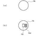
図2は、第1基板10a及び第2基板10bの平面図であり、ともに裏面側から見たものである。図2(a)に示すように、第2基板10bの裏面は穴や溝加工はされておらず、図2(b)に示すように、第1基板10aの裏面に穴10a1及び溝10a2が形成される。 FIG. 2 is a plan view of the
図3は、InGaN系LEDの製造装置である。反応室のサセプタには第1基板10aが載置されており、第1基板10aの上に第2基板10bを載置する。具体的には、第2基板10bをウェーハトレイの上に載置し、真空ゲートから反応室の内部に搬入してサセプタの上にセットする。第2基板10bは第1基板10aに対して所定量(例えば6mm)だけずれて載置され、第2基板10bのうち第1基板10a上に載置されていない部位が存在する。次に、反応室の内部を真空ポンプで減圧しながら、ヒータ100でサセプタを加熱する。そして、原料ガスを反応室に供給して第2基板10b上に順次、バッファ層12、GaN層14、Siドープのn−GaN層16、GaN層18/InGaN層20/GaN層22のSQW発光層23、Mgドープのp−AlGaN層24及びMgドープのp−GaN層26を形成する。 FIG. 3 shows an InGaN-based LED manufacturing apparatus. The
図4は、図1の構成におけるLEDのPL(フォトルミネセンス)測定結果である。横軸は波長(nm)を示し、縦軸は強度(a.u.)を示す。 FIG. 4 shows the PL (photoluminescence) measurement results of the LED in the configuration of FIG. The horizontal axis indicates the wavelength (nm), and the vertical axis indicates the intensity (au).
図4において、aは第1基板10aのうち穴10a1及び溝10a2のいずれも存在しない部位における発光スペクトルを示し、bは第1基板10aのうち溝10a2が存在する部位における発光スペクトルを示し、cは第1基板10aのうち穴10a1が存在する部位における発光スペクトルを示す。また、dは第1基板10aと第2基板10bがずれている部位、すなわち第2基板10bのうち第1基板10aが存在しない部位の発光スペクトルを示す。 In FIG. 4, a represents an emission spectrum in a portion of the
第1基板10aのうち穴10a1及び溝10a2のいずれも存在しない部位、すなわち単にサファイア基板を2重にした部位では、aに示すように発光ピーク波長は約440nmである。 In a portion of the
他方、第1基板10aのうち溝10a2が存在する部位では、bに示すように発光ピーク波長は約470nmであり、第1基板10aのうち穴10a1が存在する部位では、cに示すように発光ピーク波長は約520nmとなっている。 On the other hand, in the portion of the
発光ピーク波長で比較すると、
2重のサファイア基板の波長<溝10a2ありの波長<穴10a1ありの波長
である。これは、溝10a2が存在する場合には、その分だけ2重のサファイア基板の場合に比べてヒータ100の熱が伝わり難くなって相対的に低温となり、In組成比xが増大して長波長側にシフトし、穴10a1が存在する場合には、その分だけさらに溝10a2が存在する場合に比べてヒータ100の熱が伝わり難くなって相対的に低温となり、In組成比xがさらに増大して長波長側にシフトしたものである。溝10a2の深さを調整することで、発光ピーク波長を微調整できることは容易に理解されよう。すなわち、溝10a2の深さが0の場合には2重のサファイア基板の場合と発光ピーク波長は同一であり、溝10a2の深さが深くなるに従い発光ピーク波長は長波長側にシフトする。Compared with the peak emission wavelength,
The wavelength of the double sapphire substrate <the wavelength with the groove 10a2 <the wavelength with the hole 10a1. This is because when the groove 10a2 is present, the heat of the
このように、第2基板10bの裏面に溝を形成することなく、あるいは第2基板10bの裏面に溝を形成してチタン膜等を成膜することなく、第1基板10aの裏面に穴10a1や溝10a2を加工することで、広範囲に発光波長を調整することができる。 As described above, the hole 10a1 is formed on the back surface of the
なお、第1基板10aと第2基板10bが互いにずれており、第2基板10bのうち第1基板10aが存在しない端部の部位では、dに示すように約530nmと約600nmに発光ピーク波長が存在している。約530nmの光はGaN結晶の欠陥に起因するディープレベル(DL)からの発光であり、ヒータから離れており熱伝導率が低いため、その分発光波長が長波長側にシフトしたものと考えられる。本実施形態では、第1基板10aと第2基板10bのずれ量を所定量(6mm)としているが、第1基板10aと第2基板10bのずれ量をさらに大きくすることで発光ピーク波長はさらに長波長側にシフトしていく。 It should be noted that the
以上のように、本実施形態では、第1基板10a及び第2基板10bの2つの基板構成とすることで、第2基板10bの裏面に溝やチタン膜等を成膜することなく、発光波長を広範囲に変化(約440nmから約600nmさらにはより長波長域まで)させることができる。 As described above, in the present embodiment, the two substrate configurations of the
本発明は上記実施形態に限定されるものではなく、種々の変形が可能である。 The present invention is not limited to the above embodiment, and various modifications are possible.
例えば、本実施形態では、第1基板10aの裏面に穴10a1及び溝10a2を形成しているが、穴10a1のみを周期的または非周期的に形成してもよく、あるいは溝10a2のみを周期的または非周期的に形成してもよい。穴10a1を形成する際に、穴10a1の径を周期的に変化させてもよく、溝10a2を形成する際に、溝10a2の深さを周期的に変化させてもよい。また、溝10a2を形成する際に、その断面形状は必ずしも図1に示すような矩形である必要はなく、円形、楕円形その他の形状でもよい。さらに、第1基板10aのある領域はサファイアで構成され、他の領域はガラスで構成されていてもよい。すなわち、第1基板10aの材質は周期的または非周期的に変化していてもよい。 For example, in this embodiment, the hole 10a1 and the groove 10a2 are formed on the back surface of the
また、本実施形態では発光層23としてInGaN SQWを用いているが、InGaN MQW(多重量子井戸:Multi Quantum Well)を用いることもできる。また、発光層としてInGaNではなく、AlInGaNを用いることもできる。要するに、温度変化に対して高感度に組成が変化し、その結果発光波長が変化し得る任意のInGaN系発光層を用いることができる。本実施形態では、青色発光の発光層を用いているが、これに限らず、紫外(UV)や青緑色の発光層を用いてもよい。 In this embodiment, InGaN SQW is used as the
また、本実施形態では、第2基板10bとしてサファイア基板を用いているが、InGanあるいはAlInGaN発光層を成長させることができるGaN基板、AlN基板、あるいはSiC基板としてもよい。 In this embodiment, a sapphire substrate is used as the
また、本実施形態では、第1基板10aとしてサファイア基板ないしガラス基板を用いているが、GaN系化合物半導体層を成長させる温度で安定な任意の材料、例えばSiC、GaN、AlN等を用いてもよい。 In this embodiment, a sapphire substrate or a glass substrate is used as the
さらに、本実施形態では、第1基板10a、第2基板10bともにその厚さを330μmとしたが、これは例示であり、それぞれ1mm以下、より望ましくは0.5mm以下であればよい。第1基板10aと第2基板10bのトータルの厚さを1mm以下としてもよく、第1基板10aと第2基板10bの厚さは必ずしも同一である必要はない。 Furthermore, in the present embodiment, the thickness of both the
10a 第1基板、10b 第2基板、10a1 穴、10a2 溝、12 バッファ層、14 GaN層、16 n−GaN層、18 GaN層、20 InGaN層、22 GaN層、23 発光層、24 p−AlGaN層、26 p−GaN層、100 ヒータ。
10a 1st substrate, 10b 2nd substrate, 10a1 hole, 10a2 groove, 12 buffer layer, 14 GaN layer, 16 n-GaN layer, 18 GaN layer, 20 InGaN layer, 22 GaN layer, 23 light emitting layer, 24 p-AlGaN Layer, 26 p-GaN layer, 100 heater.
Claims (4)
Translated fromJapanese表面が平坦で裏面が加工された第1基板の表面に、表面及び裏面が平坦な第2基板を配置する工程と、
前記第1基板の裏面側から加熱しつつ、前記第2基板の表面にAlInGaNを含むInGaN系化合物半導体発光層を含むGaN系化合物半導体層を積層する工程と、
を備えることを特徴とするInGaN系化合物半導体発光装置の製造方法。A method of manufacturing an InGaN-based compound semiconductor light-emitting device containing AlInGaN,
Disposing a second substrate having a flat front surface and a back surface on the front surface of the first substrate having a flat front surface and a processed back surface;
Laminating a GaN-based compound semiconductor layer including an InGaN-based compound semiconductor light emitting layer including AlInGaN on the surface of the second substrate while heating from the back side of the first substrate;
A method for manufacturing an InGaN-based compound semiconductor light-emitting device.
前記第1基板の裏面の加工は、穴加工あるいは溝加工の少なくともいずれかであることを特徴とするInGaN系化合物半導体発光装置の製造方法。The method of claim 1, wherein
The method of manufacturing an InGaN-based compound semiconductor light-emitting device, wherein the processing of the back surface of the first substrate is at least one of hole processing and groove processing.
前記第2基板は、サファイア基板、GaN基板、AlN基板、SiC基板のいずれかである
ことを特徴とするInGaN系化合物半導体発光装置の製造方法。The method according to any one of claims 1 and 2,
The second substrate is any one of a sapphire substrate, a GaN substrate, an AlN substrate, and a SiC substrate.
前記第1基板の裏面に穴あるいは溝の少なくともいずれかを形成し、
前記第1基板の表面に、その裏面が平坦な第2基板を載置し、
前記第1基板の裏面側から加熱しつつ、前記第2基板の表面にAlInGaNを含むInGaN系化合物半導体発光層を含むGaN系化合物半導体層を積層することで、前記InGaN系化合物半導体発光層からの発光波長を調整することを特徴とするInGaN系化合物半導体発光装置の波長調整方法。
The substrate is a first substrate and a second substrate,
Forming at least one of a hole or a groove on the back surface of the first substrate;
A second substrate having a flat back surface is placed on the front surface of the first substrate;
By stacking a GaN-based compound semiconductor light-emitting layer including an InGaN-based compound semiconductor light-emitting layer containing AlInGaN on the surface of the second substrate while heating from the back side of the first substrate, A wavelength adjustment method for an InGaN-based compound semiconductor light-emitting device, characterized by adjusting an emission wavelength.
Priority Applications (1)
| Application Number | Priority Date | Filing Date | Title |
|---|---|---|---|
| JP2014166047AJP2016042534A (en) | 2014-08-18 | 2014-08-18 | Method for manufacturing indium-gallium-nitrogen-based compound semiconductor light emitting device and light wavelength adjusting method |
Applications Claiming Priority (1)
| Application Number | Priority Date | Filing Date | Title |
|---|---|---|---|
| JP2014166047AJP2016042534A (en) | 2014-08-18 | 2014-08-18 | Method for manufacturing indium-gallium-nitrogen-based compound semiconductor light emitting device and light wavelength adjusting method |
Publications (1)
| Publication Number | Publication Date |
|---|---|
| JP2016042534Atrue JP2016042534A (en) | 2016-03-31 |
Family
ID=55592154
Family Applications (1)
| Application Number | Title | Priority Date | Filing Date |
|---|---|---|---|
| JP2014166047APendingJP2016042534A (en) | 2014-08-18 | 2014-08-18 | Method for manufacturing indium-gallium-nitrogen-based compound semiconductor light emitting device and light wavelength adjusting method |
Country Status (1)
| Country | Link |
|---|---|
| JP (1) | JP2016042534A (en) |
Citations (4)
| Publication number | Priority date | Publication date | Assignee | Title |
|---|---|---|---|---|
| JP2000031595A (en)* | 1998-07-10 | 2000-01-28 | Nec Corp | Optical semiconductor element as well as method and apparatus for manufacture of optical semiconductor element |
| JP2004079867A (en)* | 2002-08-21 | 2004-03-11 | Shiro Sakai | Manufacturing method of gallium nitride base compound semiconductor device, and light emitting device |
| US20060027820A1 (en)* | 2004-07-07 | 2006-02-09 | Densen Cao | Monolitholic LED chip to emit multiple colors |
| JP2012049501A (en)* | 2010-08-30 | 2012-03-08 | Invenlux Corp | Light-emitting devices with two-dimensional composition-fluctuation active-region and method for fabricating the same |
- 2014
- 2014-08-18JPJP2014166047Apatent/JP2016042534A/enactivePending
Patent Citations (4)
| Publication number | Priority date | Publication date | Assignee | Title |
|---|---|---|---|---|
| JP2000031595A (en)* | 1998-07-10 | 2000-01-28 | Nec Corp | Optical semiconductor element as well as method and apparatus for manufacture of optical semiconductor element |
| JP2004079867A (en)* | 2002-08-21 | 2004-03-11 | Shiro Sakai | Manufacturing method of gallium nitride base compound semiconductor device, and light emitting device |
| US20060027820A1 (en)* | 2004-07-07 | 2006-02-09 | Densen Cao | Monolitholic LED chip to emit multiple colors |
| JP2012049501A (en)* | 2010-08-30 | 2012-03-08 | Invenlux Corp | Light-emitting devices with two-dimensional composition-fluctuation active-region and method for fabricating the same |
Similar Documents
| Publication | Publication Date | Title |
|---|---|---|
| CN105322064B (en) | Ultraviolet light emitting diode | |
| CN1996626B (en) | Nitride-based light emitting devices and methods of manufacturing the same | |
| CN102439740B (en) | Light emitting device | |
| KR102075987B1 (en) | Nitride semiconductor light emitting device | |
| KR102397660B1 (en) | Semiconductor light-emitting element | |
| TWI359506B (en) | Light-emitting device and manufacturing method the | |
| KR20140021715A (en) | Method of manufacture for nitride semiconductor light emitting element, wafer, and nitride semiconductor light emitting element | |
| JP2011254078A (en) | Semiconductor die, light-emitting device, method of manufacturing the same, and method of generating multiple-wavelength light | |
| WO2011125449A1 (en) | Nitrogen compound semiconductor light emitting element and manufacturing method thereof | |
| JP6457784B2 (en) | Semiconductor light emitting device | |
| JP2008047860A (en) | Method for forming surface irregularities and method for producing gallium nitride-based light emitting diode device using the same | |
| CN106415860B (en) | Nitride semiconductor light emitting device | |
| CN105514232B (en) | A kind of production method of LED epitaxial slice, light emitting diode and epitaxial wafer | |
| TW201937753A (en) | Nitride semiconductor light-emitting element | |
| JP2017112166A (en) | Semiconductor light emitting element array and vehicle lamp | |
| CN104916748A (en) | Optical semiconductor element | |
| KR101666836B1 (en) | Growth technique for phosphor-free white light emitting diode | |
| US8314436B2 (en) | Light emitting device and manufacturing method thereof | |
| US9543476B2 (en) | UV light emitting diode and method of fabricating the same | |
| JP2017017265A (en) | Light-emitting device | |
| CN105810784A (en) | Fabrication method of white-light LED | |
| JP2016042534A (en) | Method for manufacturing indium-gallium-nitrogen-based compound semiconductor light emitting device and light wavelength adjusting method | |
| JP6367590B2 (en) | LIGHT EMITTING ELEMENT AND METHOD FOR MANUFACTURING LIGHT EMITTING ELEMENT STRUCTURE | |
| KR101581438B1 (en) | manufacturing method of white LED using nanorod and white LED thereby | |
| JP2005317823A (en) | Gallium nitride system light emitting device |
Legal Events
| Date | Code | Title | Description |
|---|---|---|---|
| A621 | Written request for application examination | Free format text:JAPANESE INTERMEDIATE CODE: A621 Effective date:20170605 | |
| A521 | Request for written amendment filed | Free format text:JAPANESE INTERMEDIATE CODE: A821 Effective date:20170605 | |
| A977 | Report on retrieval | Free format text:JAPANESE INTERMEDIATE CODE: A971007 Effective date:20180314 | |
| A131 | Notification of reasons for refusal | Free format text:JAPANESE INTERMEDIATE CODE: A131 Effective date:20180410 | |
| A02 | Decision of refusal | Free format text:JAPANESE INTERMEDIATE CODE: A02 Effective date:20181106 |