JP2016040888A - Semiconductor device - Google Patents
Semiconductor deviceDownload PDFInfo
- Publication number
- JP2016040888A JP2016040888AJP2014164786AJP2014164786AJP2016040888AJP 2016040888 AJP2016040888 AJP 2016040888AJP 2014164786 AJP2014164786 AJP 2014164786AJP 2014164786 AJP2014164786 AJP 2014164786AJP 2016040888 AJP2016040888 AJP 2016040888A
- Authority
- JP
- Japan
- Prior art keywords
- node
- power supply
- switch
- semiconductor device
- circuit
- Prior art date
- Legal status (The legal status is an assumption and is not a legal conclusion. Google has not performed a legal analysis and makes no representation as to the accuracy of the status listed.)
- Granted
Links
Images


Classifications
- H—ELECTRICITY
- H03—ELECTRONIC CIRCUITRY
- H03K—PULSE TECHNIQUE
- H03K19/00—Logic circuits, i.e. having at least two inputs acting on one output; Inverting circuits
- H03K19/0008—Arrangements for reducing power consumption
- H03K19/0013—Arrangements for reducing power consumption in field effect transistor circuits
- H—ELECTRICITY
- H03—ELECTRONIC CIRCUITRY
- H03K—PULSE TECHNIQUE
- H03K17/00—Electronic switching or gating, i.e. not by contact-making and –breaking
- H03K17/51—Electronic switching or gating, i.e. not by contact-making and –breaking characterised by the components used
- H03K17/56—Electronic switching or gating, i.e. not by contact-making and –breaking characterised by the components used by the use, as active elements, of semiconductor devices
- H03K17/687—Electronic switching or gating, i.e. not by contact-making and –breaking characterised by the components used by the use, as active elements, of semiconductor devices the devices being field-effect transistors
- H03K17/693—Switching arrangements with several input- or output-terminals, e.g. multiplexers, distributors
- H—ELECTRICITY
- H03—ELECTRONIC CIRCUITRY
- H03K—PULSE TECHNIQUE
- H03K19/00—Logic circuits, i.e. having at least two inputs acting on one output; Inverting circuits
- H03K19/0008—Arrangements for reducing power consumption
- H03K19/0016—Arrangements for reducing power consumption by using a control or a clock signal, e.g. in order to apply power supply
- H—ELECTRICITY
- H03—ELECTRONIC CIRCUITRY
- H03K—PULSE TECHNIQUE
- H03K19/00—Logic circuits, i.e. having at least two inputs acting on one output; Inverting circuits
- H03K19/0175—Coupling arrangements; Interface arrangements
- H03K19/0185—Coupling arrangements; Interface arrangements using field effect transistors only
- H03K19/018507—Interface arrangements
- H03K19/018521—Interface arrangements of complementary type, e.g. CMOS
Landscapes
- Engineering & Computer Science (AREA)
- Computer Hardware Design (AREA)
- Physics & Mathematics (AREA)
- Computing Systems (AREA)
- General Engineering & Computer Science (AREA)
- Mathematical Physics (AREA)
- Semiconductor Integrated Circuits (AREA)
- Logic Circuits (AREA)
Abstract
Description
Translated fromJapanese本発明は、半導体装置に関する。 The present invention relates to a semiconductor device.
半導体装置の消費電力を抑えるため、所定の回路ノードへの電力供給を遮断するパワーゲーティングと呼ばれる手法が知られている(例えば、特許文献1を参照)。 In order to reduce the power consumption of the semiconductor device, a technique called power gating that cuts off power supply to a predetermined circuit node is known (see, for example, Patent Document 1).
しかしながら、従来技術では、電圧値が異なる複数の電源からの電力供給についてパワーゲーティングをする場合、パワーゲーティングを制御する制御部を各電源に用意する必要があるため、半導体装置の消費電力が制御部の個数に比例して増加する。 However, in the prior art, when power gating is performed for power supply from a plurality of power sources having different voltage values, it is necessary to prepare a control unit for controlling power gating in each power source. It increases in proportion to the number of.
そこで、電圧値が異なる複数の電源からの電力供給についてパワーゲーティングをする場合において、低消費電力化が可能な、半導体装置の提供を目的とする。 Therefore, an object is to provide a semiconductor device capable of reducing power consumption when power gating is performed for power supply from a plurality of power supplies having different voltage values.
一つの案では、
第1の電源ノードと、
前記第1の電源ノードよりも電圧値が高い第2の電源ノードと、
前記第1の電源ノードから第1の回路ノードに供給される電力を遮断する第1のスイッチと、
前記第2の電源ノードから第2の回路ノードに供給される電力を遮断する第2のスイッチと、
前記第2の電源ノードと前記第1の回路ノードとの間に接続される第3のスイッチが駆動されることによって前記第2のスイッチを駆動するバッファと、
前記第1のスイッチと前記第3のスイッチを駆動する共通の制御信号を出力する制御部とを備える、半導体装置が提供される。One idea is that
A first power supply node;
A second power supply node having a voltage value higher than that of the first power supply node;
A first switch for cutting off power supplied from the first power supply node to the first circuit node;
A second switch for cutting off power supplied from the second power supply node to the second circuit node;
A buffer that drives the second switch by driving a third switch connected between the second power supply node and the first circuit node;
A semiconductor device is provided that includes a control unit that outputs a common control signal for driving the first switch and the third switch.
一態様によれば、半導体装置の消費電力の低減が可能である。 According to one embodiment, power consumption of a semiconductor device can be reduced.
以下、実施形態を図面に従って説明する。 Hereinafter, embodiments will be described with reference to the drawings.
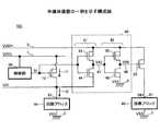
図1は、半導体装置101の一例を示す構成図である。半導体装置101は、例えば、LSI(Large Scale Integrated circuit:大規模集積回路)である。半導体装置101は、例えば、電源ノード1と、電源ノード2と、PMOSトランジスタ10と、PMOSトランジスタ20と、バッファ40と、制御部30と、グランドノード3とを備える。 FIG. 1 is a configuration diagram illustrating an example of the
なお、PMOSトランジスタとは、Pチャネル型のMOS(Metal-Oxide-Semiconductor)電界効果トランジスタであり、NMOSトランジスタとは、Nチャネル型のMOS電界効果トランジスタである。 The PMOS transistor is a P-channel MOS (Metal-Oxide-Semiconductor) field effect transistor, and the NMOS transistor is an N-channel MOS field effect transistor.
電源ノード1は、第1の電源ノードの一例であり、電源電圧VDDLの直流電力を供給可能な第1の高電源電位部である。電源電圧VDDLは、電源ノード1とグランドノード3との間の電位差である。グランドノード3は、グランド電圧VSSを有するグランド電位部である。 The
電源ノード2は、第1の電源ノードよりも電圧値が高い第2の電源ノードの一例であり、電源ノード1の電源電圧VDDLよりも高い電源電圧VDDHの直流電力を供給可能な第2の高電源電位部である。電源電圧VDDHは、電源ノード2とグランドノード3との間の電位差である。 The
PMOSトランジスタ10は、第1の電源ノードから第1の回路ノードに供給される電力を遮断する第1のスイッチの一例であり、電源ノード1から回路ノード51に供給される電力を遮断可能な半導体スイッチング素子である。 The
PMOSトランジスタ20は、第2の電源ノードから第2の回路ノードに供給される電力を遮断する第2のスイッチの一例であり、電源ノード2から回路ノード61に供給される電力を遮断可能な半導体スイッチング素子である。 The
バッファ40は、第2の電源ノードと第1の回路ノードとの間に接続される第3のスイッチが駆動されることによって第2のスイッチを駆動するバッファの一例である。バッファ40は、例えば、電源ノード2と回路ノード51との間に接続されるCMOSインバータ41が駆動されることによってPMOSトランジスタ20をオンオフ駆動する回路である。CMOSインバータ41は、第3のスイッチの一例である。 The
なお、CMOSとは、「Complementary MOS」の略である。 CMOS is an abbreviation for “Complementary MOS”.
制御部30は、第1のスイッチと第3のスイッチを駆動する共通の制御信号を出力する制御部の一例である。制御部30は、例えば、PMOSトランジスタ10とCMOSインバータ41をオンオフ駆動する共通の制御信号S1を出力する回路である。 The
したがって、本実施形態によれば、電源ノード1から回路ノード51への電力供給を遮断する制御と、電源ノード2から回路ノード61への電力供給を遮断する制御とを一つの共通の制御部30によって実行可能である。つまり、電力供給を遮断すべき系統が複数あっても、制御部30の個数を抑えることができるため、半導体装置101の低消費電力化が可能である。 Therefore, according to the present embodiment, the control for cutting off the power supply from the
次に、図1の構成について、より詳細に説明する。 Next, the configuration of FIG. 1 will be described in more detail.
PMOSトランジスタ10は、制御信号S1が入力されるゲートと、電源ノード1に接続されるドレイン及びバックゲートと、回路ノード51に接続されるドレインとを有する。PMOSトランジスタ10は、制御信号S1の電圧レベルに従って、オンオフする。 The
回路ノード51は、所定の回路ブロック50に供給される電力が入力されるノードである。回路ブロック50は、回路ノード51とグランドノード3との間に接続される任意の回路であり、単数又は複数の素子によって構成される。 The
バッファ40は、制御信号S1が入力されるCMOSインバータ41と、CMOSインバータ41の出力が入力されるCMOSインバータ42とを有する。 The
CMOSインバータ41は、直列に接続されたNMOSトランジスタ44とPMOSトランジスタ43とを有する。NMOSトランジスタ44は、制御信号S1が入力されるゲートと、回路ノード51に接続されるソース及びバックゲートと、CMOSインバータ41の出力ノード47に接続されるドレインとを有する。PMOSトランジスタ43は、制御信号S1が入力されるゲートと、電源ノード2に接続されるソース及びバックゲートと、CMOSインバータ41の出力ノード47に接続されるドレインとを有する。 The
CMOSインバータ42は、第4のスイッチの一例であり、PMOSトランジスタ20をオンオフ駆動する。CMOSインバータ42は、直列に接続されたNMOSトランジスタ46とPMOSトランジスタ45とを有する。NMOSトランジスタ46は、出力ノード47が接続されるゲートと、グランドノード3に接続されるソース及びバックゲートと、CMOSインバータ42の出力ノード48に接続されるドレインとを有する。PMOSトランジスタ45は、出力ノード47が接続されるゲートと、電源ノード2に接続されるソース及びバックゲートと、CMOSインバータ42の出力ノード48に接続されるドレインとを有する。 The
PMOSトランジスタ20は、出力ノード48が接続されるゲートと、電源ノード2が接続されるソース及びバックゲートと、回路ノード61に接続されるドレインとを有する。バッファ40の最後段に設けられたCMOSインバータ42の出力が、PMOSトランジスタ20のゲートに入力される。
回路ノード61は、所定の回路ブロック60に供給される電力が入力されるノードである。回路ブロック60は、電源ノード2とグランドノード3との間に接続される任意の回路であり、単数又は複数の素子によって構成される。図示の場合、回路ブロック60は、PMOSトランジスタ20のドレインとグランドノード3との間に接続される。 The
制御部30は、電源ノード1から給電されるPMU(Power Management Unit)であり、電源電圧VDDLで動作する。制御部30は、電源ノード1とグランドノード3との間に接続される。 The
制御部30は、電源電圧VDDHで動作するのではなく電源電圧VDDLで動作するので、電源電圧VDDLをハイレベルとする制御信号S1をPMOSトランジスタ10のゲートに向けて出力する。制御部30が電源電圧VDDHで動作する場合、制御信号S1のハイレベルは電源電圧VDDHになる。したがって、制御部30が電源電圧VDDLで動作することによって、PMOSトランジスタ10のゲート耐圧を電源電圧VDDHよりも下げることができる。 Since the
図2は、半導体装置101の動作の一例を示すタイミングチャートである。図1を参照して、図2について説明する。 FIG. 2 is a timing chart showing an example of the operation of the
制御信号S1の電圧レベルがローレベルのグランド電圧VSSである場合、PMOSトランジスタ10はオンするので、回路ノード51の電圧V51は、電源電圧VDDLである。また、制御信号S1の電圧レベルがローレベルのグランド電圧VSSである場合、PMOSトランジスタ43はオン、NMOSトランジスタ44はオフするので、出力ノード47の電圧V47は、電源電圧VDDHである。電圧V47が電源電圧VDDHである場合、PMOSトランジスタ45はオフ、NMOSトランジスタ46はオンするので、出力ノード48の電圧V48は、グランド電圧VSSである。電圧V48がグランド電圧VSSである場合、PMOSトランジスタ20はオンするので、回路ノード61の電圧V61は、電源電圧VDDHである。 When the voltage level of the control signal S1 is the low level ground voltage VSS, the
つまり、制御信号S1の電圧レベルがローレベルのグランド電圧VSSであるタイミングt1までの期間では、回路ノード51と回路ノード61のいずれにも給電されるので、パワーゲーティング機能はオフする。 That is, during the period up to the timing t1 when the voltage level of the control signal S1 is the low level ground voltage VSS, power is supplied to both the
一方、制御信号S1の電圧レベルがハイレベルの電源電圧VDDLである場合、PMOSトランジスタ10はオフするので、回路ノード51の電圧V51は、グランド電圧VSSである。PMOSトランジスタ10のリーク電流I1と回路ブロック50のリーク電流I2とがPMOSトランジスタ10によって平衡するが、PMOSトランジスタ10のコンダクタンスは回路ブロック50のコンダクタンスよりも小さい。そのため、PMOSトランジスタ10のソース−ドレイン間の電圧が電源電圧VDDLに近づき、回路ブロック50の両端電圧がグランド電圧VSSに近づくため、回路ノード51の電圧V51は、ほぼグランド電圧VSSとなる。 On the other hand, when the voltage level of the control signal S1 is the high-level power supply voltage VDDL, the
また、制御信号S1の電圧レベルがハイレベルの電源電圧VDDLである場合、PMOSトランジスタ43はオフ、NMOSトランジスタ44はオンするので、出力ノード47の電圧V47は、グランド電圧VSSである。電圧V47がグランド電圧VSSである場合、PMOSトランジスタ45はオン、NMOSトランジスタ46はオフするので、出力ノード48の電圧V48は、電源電圧VDDHである。電圧V48が電源電圧VDDHである場合、PMOSトランジスタ20はオフするので、回路ノード61の電圧V61は、電圧V51と同様の上述の理由で、グランド電圧VSSである。 When the voltage level of the control signal S1 is the high-level power supply voltage VDDL, the
つまり、制御信号S1の電圧レベルがハイレベルの電源電圧VDDLであるタイミングt2以降の期間では、回路ノード51と回路ノード61のいずれにも給電されないので、パワーゲーティング機能はオンする。 That is, in the period after the timing t2 when the voltage level of the control signal S1 is the high-level power supply voltage VDDL, power is not supplied to either the
図3は、半導体装置101に使用されるPMOSとNMOSの両方のトランジスタの特性の一例を示す図である。図3の(A)は、PMOSトランジスタがオフする際の特性の一例を示し、図3の(B)は、NMOSトランジスタがオンする際の特性の一例を示す。Vthは、トランジスタのゲート閾値電圧、Vgsは、トランジスタのゲート−ソース間に印加される電圧、Idsは、トランジスタのドレイン−ソース間に流れる電流、Logは、常用対数、1.E−nは(nは正の整数)、1.0×10−nを表す。なお、図示の具体的な数値は、トランジスタのオンオフの動作を説明しやすくするための便宜的な値である。FIG. 3 is a diagram illustrating an example of characteristics of both PMOS and NMOS transistors used in the
制御信号S1の電圧レベルがハイレベルの電源電圧VDDLである場合、CMOSインバータ41のPMOSトランジスタ43の電圧Vgsは、ゲート閾値電圧Vthよりも低い電圧(VDDL−VDDH)であるため、PMOSトランジスタ43は、オフする(図3の(A)参照)。また、制御信号S1の電圧レベルがハイレベルの電源電圧VDDLである場合、CMOSインバータ41のNMOSトランジスタ44の電圧Vgsは、ゲート閾値電圧Vthよりも高い電圧(VDDL−VSS)であるため、NMOSトランジスタ44はオンする(図3の(B)参照)。 When the voltage level of the control signal S1 is the high-level power supply voltage VDDL, the voltage Vgs of the
しかしながら、PMOSトランジスタ43の電圧Vgsは、ゲート閾値電圧Vthよりも低い電圧(VDDL−VDDH)であるが、零ではない。そのため、PMOSトランジスタ43の電流Idsのリーク量は、電圧Vgsが零である場合に比べて多い。 However, the voltage Vgs of the
そこで、PMOSトランジスタ43のゲート閾値電圧Vthの絶対値を、NMOSトランジスタ44のゲート閾値電圧Vthよりも高くする。これにより、PMOSトランジスタ43のオフ時の特性は図4に示されるように変化する。 Therefore, the absolute value of the gate threshold voltage Vth of the
図4において、実線は、PMOSトランジスタ43のゲート閾値電圧Vthの絶対値とNMOSトランジスタ44のゲート閾値電圧Vthとが同じ電圧値(例えば、0.6V)である場合を示す。破線は、PMOSトランジスタ43のゲート閾値電圧Vthの絶対値がNMOSトランジスタ44のゲート閾値電圧Vthよりも高い場合(例えば、PMOSトランジスタ43のゲート閾値電圧Vthの絶対値が0.9Vであり、NMOSトランジスタ44のゲート閾値電圧Vthが0.6Vである場合)を示す。 In FIG. 4, the solid line indicates a case where the absolute value of the gate threshold voltage Vth of the
このように、PMOSトランジスタ43の電圧Vgsが同じであっても、PMOSトランジスタ43のゲート閾値電圧Vthの絶対値を、NMOSトランジスタ44のゲート閾値電圧Vthよりも高くすることによって、PMOSトランジスタ43の電流Idsのリーク量を減らすことができる。その結果、半導体装置101の低消費電力化が可能となる。 As described above, even if the voltage Vgs of the
図5は、半導体装置101に使用されるPMOSとNMOSの両方のトランジスタの特性の一例を示す図である。図5の(A)は、PMOSトランジスタがオンする際の特性の一例を示し、図5の(B)は、NMOSトランジスタがオフする際の特性の一例を示す。Vthは、トランジスタのゲート閾値電圧、Vgsは、トランジスタのゲート−ソース間に印加される電圧、Idsは、トランジスタのドレイン−ソース間に流れる電流、Logは、常用対数、1.E−nは(nは正の整数)、1.0×10−nを表す。なお、図示の具体的な数値は、トランジスタのオンオフの動作を説明しやすくするための便宜的な値である。FIG. 5 is a diagram illustrating an example of characteristics of both PMOS and NMOS transistors used in the
制御信号S1の電圧レベルがローレベルのグランド電圧VSSである場合、CMOSインバータ41のPMOSトランジスタ43の電圧Vgsは、ゲート閾値電圧Vthよりも高い電圧(VSS−VDDH)であるため、PMOSトランジスタ43は、オンする(図5の(A)参照)。また、制御信号S1の電圧レベルがローレベルのグランド電圧VSSである場合、CMOSインバータ41のNMOSトランジスタ44の電圧Vgsは、ゲート閾値電圧Vthよりも低い負電圧(VSS−VDDL)であるため、NMOSトランジスタ44は、オフする(図5の(B)参照)。したがって、パワーゲーティング機能のオフ時に、NMOSトランジスタ44の電圧Vgsを負電圧にできるため、図5の(B)に示されるように、電圧Vgsが例えば零である場合に比べて、NMOSトランジスタ44の電流Idsのリーク量を減らすことができる。その結果、半導体装置101の低消費電力化が可能となる。 When the voltage level of the control signal S1 is the low-level ground voltage VSS, the voltage Vgs of the
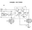
図6は、半導体装置102の一例を示す構成図である。上述の半導体装置と同様の構成及び効果についての説明は省略する。図6は、図1に示した回路ノード51,61の具体例を示す。回路ノード51,61は、例えば、回路ブロック70の回路ノードである。 FIG. 6 is a configuration diagram illustrating an example of the
半導体装置102は、回路ノード51とグランドノード3との間に接続された回路ブロック70を備える。回路ブロック70は、PMOSトランジスタ71とNMOSトランジスタ72とを有する組み合わせ回路の一例である。NMOSトランジスタ72は、半導体装置102の基板に形成されたPウェル用の電源電圧VPWが入力されるバックゲート73を有する。PMOSトランジスタ71は、半導体装置102の基板に形成されたNウェル用の電源電圧V61が入力されるバックゲートを有する。回路ノード51は、PMOSトランジスタ71のソースに接続され、回路ノード61は、PMOSトランジスタ71のバックゲートに接続される。 The
制御信号S1の電圧レベルがハイレベルの電源電圧VDDLである場合、PMOSトランジスタ10がオフすることにより、回路ノード51の電圧V51は、ほぼグランド電圧VSSになる。そのため、PMOSトランジスタ71のバックゲートとグランドノード3との間でのジャンクションリークが増大する。しかしながら、この場合、PMOSトランジスタ20もオフするので、このジャンクションリークの増大を抑制することができる。 When the voltage level of the control signal S1 is the high-level power supply voltage VDDL, the
図7は、半導体装置103の一例を示す構成図である。上述の半導体装置と同様の構成及び効果についての説明は省略する。図7は、図1の構成に対して、バッファ140の構成が異なる場合を示す。 FIG. 7 is a configuration diagram illustrating an example of the
バッファ140は、第2の電源ノードと第1の回路ノードとの間に接続される第3のスイッチが駆動されることによって第2のスイッチを駆動するバッファの一例である。バッファ140は、例えば、電源ノード2と回路ノード51との間に接続されるCMOSインバータ141が駆動されることによってPMOSトランジスタ20を駆動する回路である。CMOSインバータ141は、第3のスイッチの一例である。 The
バッファ140は、制御信号S1が入力されるCMOSインバータ141を有する。CMOSインバータ141は、直列に接続されたNMOSトランジスタ144とPMOSトランジスタ143とを有する。NMOSトランジスタ144は、制御信号S1が入力されるゲートと、回路ノード51に接続されるソース及びバックゲートと、バッファ140の出力ノード148に接続されるドレインとを有する。PMOSトランジスタ143は、制御信号S1が入力されるゲートと、電源ノード2に接続されるソース及びバックゲートと、出力ノード148に接続されるドレインとを有する。出力ノード148は、PMOSトランジスタ20のゲートに接続される。 The
半導体装置103によれば、PMOSトランジスタ10がオンのとき、PMOSトランジスタ20がオフとなり、PMOSトランジスタ10がオフのとき、PMOSトランジスタ20がオンとなる。したがって、回路ノード51に供給される電力を遮断する期間と回路ノード61に供給される電力を遮断する期間とを互い違いに異ならせることができる。 According to the
図8は、半導体装置104の一例を示す構成図である。上述の半導体装置と同様の構成及び効果についての説明は省略する。 FIG. 8 is a configuration diagram illustrating an example of the
NMOSトランジスタ21は、第2の電源ノードから第2の回路ノードに供給される電力を遮断する第2のスイッチの一例であり、電源ノード2から回路ノード62に供給される電力を遮断可能な半導体スイッチング素子である。NMOSトランジスタ21は、出力ノード148が接続されるゲートと、グランドノード3が接続されるソース及びバックゲートと、回路ノード62に接続されるドレインとを有する。回路ノード62は、所定の回路ブロック60に供給される電力が出力されるノードである。 The
半導体装置104によれば、PMOSトランジスタ10がオンのとき、NMOSトランジスタ21がオンとなり、PMOSトランジスタ10がオフのとき、NMOSトランジスタ21がオフとなる。NMOSトランジスタ21がオンのとき、回路ノード62の電圧V62は、ほぼグランド電圧VSSになり、電源ノード2から回路ブロック60及び回路ノード62への給電が可能となる。NMOSトランジスタ21がオフのとき、回路ノード62の電圧V62は、ほぼ電源電圧VDDHになり、電源ノード2から回路ブロック60及び回路ノード62への給電が遮断される。したがって、半導体装置101と同様に、回路ノード51に供給される電力の遮断と回路ノード62に供給される電力の遮断とを同時に実行することができる。 According to the
図9は、半導体装置105の一例を示す構成図である。上述の半導体装置と同様の構成及び効果についての説明は省略する。 FIG. 9 is a configuration diagram illustrating an example of the
バッファ40は、CMOSインバータ41が駆動されることによって、NMOSトランジスタ21及びPMOSトランジスタ20を駆動する。NMOSトランジスタ21は、CMOSインバータ41の駆動によってオンオフし、PMOSトランジスタ20は、CMOSインバータ42の駆動によってオンオフする。出力ノード47は、NMOSトランジスタ21のゲートに接続され、出力ノード48は、PMOSトランジスタ22のゲートに接続される。 The
半導体装置105によれば、PMOSトランジスタ10がオンのとき、PMOSトランジスタ20及びNMOSトランジスタ21がオンとなり、PMOSトランジスタ10がオフのとき、PMOSトランジスタ20及びNMOSトランジスタ21がオフとなる。したがって、半導体装置101と同様に、回路ノード51に供給される電力の遮断と回路ノード61,62に供給される電力の遮断とを同時に実行することができる。 According to the
図10は、半導体装置106の一例を示す構成図である。上述の半導体装置と同様の構成及び効果についての説明は省略する。半導体装置106は、電源ノード4と、PMOSトランジスタ22と、バッファ80と、回路ノード91とを備える。 FIG. 10 is a configuration diagram illustrating an example of the
電源ノード4は、第2の電源ノードよりも電圧値が高い第3の電源ノードの一例であり、電源ノード2の電源電圧VDDH1よりも高い電源電圧VDDH2の直流電力を供給可能な第3の高電源電位部である。電源電圧VDDH2は、電源ノード4とグランドノード3との間の電位差である。電源電圧VDDH1と電源電圧VDDH2の電圧値は、互いに等しくてもよい。 The power supply node 4 is an example of a third power supply node having a voltage value higher than that of the second power supply node. The third power supply node 4 can supply DC power of the power supply voltage VDDH2 higher than the power supply voltage VDDH1 of the
PMOSトランジスタ22は、第3の電源ノードから第3の回路ノード91に供給される電力を遮断する第5のスイッチの一例であり、電源ノード4から回路ノード91に供給される電力を遮断可能な半導体スイッチング素子である。 The PMOS transistor 22 is an example of a fifth switch that cuts off power supplied from the third power supply node to the
回路ノード91は、所定の回路ブロック90に供給される電力が入力されるノードである。回路ブロック90は、回路ノード91とグランドノード3との間に接続される任意の回路であり、単数又は複数の素子によって構成される。 The
バッファ80は、第3の電源ノードと第1の回路ノードとの間に接続される第6のスイッチが駆動されることによって第5のスイッチを駆動する第2のバッファの一例である。バッファ80は、例えば、電源ノード4と回路ノード51との間に接続されるCMOSインバータ81が駆動されることによってPMOSトランジスタ22を駆動する回路である。CMOSインバータ81は、第6のスイッチの一例である。 The
バッファ80は、制御信号S1が入力されるCMOSインバータ81と、CMOSインバータ81の出力が入力されるCMOSインバータ82とを有する。制御信号S1は、PMOSトランジスタ10とCMOSインバータ41とCMOSインバータ81とに共通の信号である。 The
バッファ80は、バッファ40の構成と同様である。例えば、CMOSインバータ81は、NMOSトランジスタ84と、ゲート閾値電圧の絶対値がNMOSトランジスタ84のゲート閾値電圧よりも高いPMOSトランジスタ83とを有する。これにより、PMOSトランジスタ83の電流Idsのリーク量を減らすことができる。バッファ80は、CMOSインバータ82を電源ノード4とグランドノード3との間に有する。CMOSインバータ82は、PMOSトランジスタ22を駆動する第7のスイッチの一例である。PMOSトランジスタ22のゲートは、バッファ80のCMOSインバータ82の出力ノード88に接続される。 The
したがって、電圧値の異なる電源ノードの数が2つ又は3つ以上に増えても、制御部30の個数を抑えて、各電源ノードについてパワーゲーティングの制御が可能となる。 Therefore, even if the number of power supply nodes having different voltage values is increased to two or three or more, it is possible to control the power gating for each power supply node while suppressing the number of
以上、半導体装置を実施形態により説明したが、本発明は上記実施形態に限定されるものではない。他の実施形態の一部又は全部との組み合わせや置換などの種々の変形及び改良が、本発明の範囲内で可能である。 Although the semiconductor device has been described above by way of the embodiment, the present invention is not limited to the above embodiment. Various modifications and improvements such as combinations and substitutions with some or all of the other embodiments are possible within the scope of the present invention.
以上の実施形態に関し、更に以下の付記を開示する。
(付記1)
第1の電源ノードと、
前記第1の電源ノードよりも電圧値が高い第2の電源ノードと、
前記第1の電源ノードから第1の回路ノードに供給される電力を遮断する第1のスイッチと、
前記第2の電源ノードから第2の回路ノードに供給される電力を遮断する第2のスイッチと、
前記第2の電源ノードと前記第1の回路ノードとの間に接続される第3のスイッチが駆動されることによって前記第2のスイッチを駆動するバッファと、
前記第1のスイッチと前記第3のスイッチを駆動する共通の制御信号を出力する制御部とを備える、半導体装置。
(付記2)
前記第3のスイッチは、CMOSインバータである、付記1に記載の半導体装置。
(付記3)
前記CMOSインバータは、NMOSトランジスタと、ゲート閾値電圧の絶対値が当該NMOSトランジスタのゲート閾値電圧よりも高いPMOSトランジスタとを有する、付記2に記載の半導体装置。
(付記4)
前記バッファは、前記第2のスイッチを駆動する第4のスイッチを前記第2の電源ノードとグランドノードとの間に有する、付記3に記載の半導体装置。
(付記5)
前記第4のスイッチは、第2のCMOSインバータである、付記4に記載の半導体装置。
(付記6)
前記第2のスイッチは、前記第3のスイッチによって駆動されるNMOSトランジスタと、前記第4のスイッチによって駆動されるPMOSトランジスタとを有する、付記5に記載の半導体装置。
(付記7)
前記第2のスイッチは、PMOSトランジスタである、付記1から3のいずれか一つに記載の半導体装置。
(付記8)
前記第2のスイッチは、NMOSトランジスタである、付記1から3のいずれか一つに記載の半導体装置。
(付記9)
前記制御部は、前記第1の電源ノードから給電される、付記1から8のいずれか一項に記載の半導体装置。
(付記10)
前記第1の回路ノード及び前記第2の回路ノードは、第1の回路ブロックの回路ノードであり、
前記第1の回路ノードは、前記第1の回路ブロックに含まれるPMOSトランジスタのソースに接続され、
前記第2の回路ノードは、当該POSトランジスタのバックゲートに接続される、付記1から9のいずれか一つに記載の半導体装置。
(付記11)
前記第2の電源ノードよりも電圧値が高い第3の電源ノードと、
前記第3の電源ノードから第3の回路ノードに供給される電力を遮断する第5のスイッチと、
前記第3の電源ノードと前記第1の回路ノードとの間に接続される第6のスイッチが駆動されることによって前記第5のスイッチを駆動する第2のバッファとを備え、
前記制御信号は、前記第1のスイッチと前記第3のスイッチと前記6のスイッチとに共通の信号である、付記1から10のいずれか一つに記載の半導体装置。
(付記12)
前記第6のスイッチは、第3のCMOSインバータである、付記11に記載の半導体装置。
(付記13)
前記第3のCMOSインバータは、NMOSトランジスタと、ゲート閾値電圧の絶対値が当該NMOSトランジスタのゲート閾値電圧よりも高いPMOSトランジスタとを有する、付記12に記載の半導体装置。
(付記14)
前記第2のバッファは、前記第5のスイッチを駆動する第7のスイッチを前記第3の電源ノードとグランドノードとの間に有する、付記13に記載の半導体装置。
(付記15)
前記第7のスイッチは、CMOSインバータである、付記14に記載の半導体装置。Regarding the above embodiment, the following additional notes are disclosed.
(Appendix 1)
A first power supply node;
A second power supply node having a voltage value higher than that of the first power supply node;
A first switch for cutting off power supplied from the first power supply node to the first circuit node;
A second switch for cutting off power supplied from the second power supply node to the second circuit node;
A buffer that drives the second switch by driving a third switch connected between the second power supply node and the first circuit node;
A semiconductor device comprising: a control unit that outputs a common control signal for driving the first switch and the third switch.
(Appendix 2)
The semiconductor device according to
(Appendix 3)
The semiconductor device according to
(Appendix 4)
4. The semiconductor device according to
(Appendix 5)
The semiconductor device according to appendix 4, wherein the fourth switch is a second CMOS inverter.
(Appendix 6)
The semiconductor device according to
(Appendix 7)
The semiconductor device according to any one of
(Appendix 8)
4. The semiconductor device according to any one of
(Appendix 9)
The semiconductor device according to any one of
(Appendix 10)
The first circuit node and the second circuit node are circuit nodes of a first circuit block;
The first circuit node is connected to a source of a PMOS transistor included in the first circuit block;
The semiconductor device according to any one of
(Appendix 11)
A third power supply node having a voltage value higher than that of the second power supply node;
A fifth switch for cutting off power supplied from the third power supply node to the third circuit node;
A second buffer for driving the fifth switch by driving a sixth switch connected between the third power supply node and the first circuit node;
The semiconductor device according to any one of
(Appendix 12)
The semiconductor device according to
(Appendix 13)
The semiconductor device according to
(Appendix 14)
14. The semiconductor device according to appendix 13, wherein the second buffer has a seventh switch that drives the fifth switch between the third power supply node and a ground node.
(Appendix 15)
The semiconductor device according to
1,2,4電源ノード
3 グランドノード
10,20,22 PMOSトランジスタ
21 NMOSトランジスタ
30 制御部
40,80,140 バッファ
41,42,81,82,141 CMOSインバータ
51,61,62,91 回路ノード
101,102,103,104,105,106 半導体装置1, 2, 4
Claims (7)
Translated fromJapanese前記第1の電源ノードよりも電圧値が高い第2の電源ノードと、
前記第1の電源ノードから第1の回路ノードに供給される電力を遮断する第1のスイッチと、
前記第2の電源ノードから第2の回路ノードに供給される電力を遮断する第2のスイッチと、
前記第2の電源ノードと前記第1の回路ノードとの間に接続される第3のスイッチが駆動されることによって前記第2のスイッチを駆動するバッファと、
前記第1のスイッチと前記第3のスイッチを駆動する共通の制御信号を出力する制御部とを備える、半導体装置。A first power supply node;
A second power supply node having a voltage value higher than that of the first power supply node;
A first switch for cutting off power supplied from the first power supply node to the first circuit node;
A second switch for cutting off power supplied from the second power supply node to the second circuit node;
A buffer that drives the second switch by driving a third switch connected between the second power supply node and the first circuit node;
A semiconductor device comprising: a control unit that outputs a common control signal for driving the first switch and the third switch.
前記第1の回路ノードは、前記第1の回路ブロックに含まれるPMOSトランジスタのソースに接続され、
前記第2の回路ノードは、当該PMOSトランジスタのバックゲートに接続される、請求項1から6のいずれか一項に記載の半導体装置。The first circuit node and the second circuit node are circuit nodes of a first circuit block;
The first circuit node is connected to a source of a PMOS transistor included in the first circuit block;
The semiconductor device according to claim 1, wherein the second circuit node is connected to a back gate of the PMOS transistor.
Priority Applications (2)
| Application Number | Priority Date | Filing Date | Title |
|---|---|---|---|
| JP2014164786AJP6417781B2 (en) | 2014-08-13 | 2014-08-13 | Semiconductor device |
| US14/797,885US9692415B2 (en) | 2014-08-13 | 2015-07-13 | Semiconductor device having low power consumption |
Applications Claiming Priority (1)
| Application Number | Priority Date | Filing Date | Title |
|---|---|---|---|
| JP2014164786AJP6417781B2 (en) | 2014-08-13 | 2014-08-13 | Semiconductor device |
Publications (2)
| Publication Number | Publication Date |
|---|---|
| JP2016040888Atrue JP2016040888A (en) | 2016-03-24 |
| JP6417781B2 JP6417781B2 (en) | 2018-11-07 |
Family
ID=55302909
Family Applications (1)
| Application Number | Title | Priority Date | Filing Date |
|---|---|---|---|
| JP2014164786AExpired - Fee RelatedJP6417781B2 (en) | 2014-08-13 | 2014-08-13 | Semiconductor device |
Country Status (2)
| Country | Link |
|---|---|
| US (1) | US9692415B2 (en) |
| JP (1) | JP6417781B2 (en) |
Cited By (1)
| Publication number | Priority date | Publication date | Assignee | Title |
|---|---|---|---|---|
| JPWO2020079572A1 (en)* | 2018-10-18 | 2021-12-23 | 株式会社半導体エネルギー研究所 | Semiconductor devices, semiconductor wafers, and electronic devices |
Families Citing this family (3)
| Publication number | Priority date | Publication date | Assignee | Title |
|---|---|---|---|---|
| US10742211B1 (en)* | 2019-07-31 | 2020-08-11 | Google Llc | Power sequencing in an active silicon interposer |
| US12228952B2 (en)* | 2022-05-02 | 2025-02-18 | Apple Inc. | Electronic devices having complementary current mirror circuitry |
| US12235781B2 (en)* | 2022-12-30 | 2025-02-25 | Parade Technologies, Ltd. | Power consumption control for transmitters of retimers in high speed data communication |
Citations (6)
| Publication number | Priority date | Publication date | Assignee | Title |
|---|---|---|---|---|
| JPH05327466A (en)* | 1992-05-18 | 1993-12-10 | Mitsubishi Electric Corp | Level conversion circuit |
| JP2003168735A (en)* | 2001-11-30 | 2003-06-13 | Hitachi Ltd | Semiconductor integrated circuit device |
| JP2007329507A (en)* | 2007-08-31 | 2007-12-20 | Renesas Technology Corp | Semiconductor device |
| JP2008042763A (en)* | 2006-08-09 | 2008-02-21 | Toshiba Corp | Semiconductor integrated circuit |
| JP2008072349A (en)* | 2006-09-13 | 2008-03-27 | Elpida Memory Inc | Semiconductor device |
| JP2012114504A (en)* | 2010-11-19 | 2012-06-14 | Renesas Electronics Corp | Power switch circuit |
Family Cites Families (11)
| Publication number | Priority date | Publication date | Assignee | Title |
|---|---|---|---|---|
| JPH09172367A (en) | 1995-12-20 | 1997-06-30 | Seiko Epson Corp | Level shifter circuit |
| JP3179350B2 (en) | 1996-09-09 | 2001-06-25 | 日本電気株式会社 | Level shift circuit |
| JP3019805B2 (en)* | 1997-06-19 | 2000-03-13 | 日本電気株式会社 | CMOS logic circuit |
| JP2001186007A (en)* | 1999-12-24 | 2001-07-06 | Sharp Corp | Metal oxide semiconductor transistor circuit and semiconductor integrated circuit using the same |
| JP4435553B2 (en)* | 2003-12-12 | 2010-03-17 | パナソニック株式会社 | Semiconductor device |
| US7292061B2 (en)* | 2005-09-30 | 2007-11-06 | Masaid Technologies Incorporated | Semiconductor integrated circuit having current leakage reduction scheme |
| US7723867B2 (en)* | 2007-05-31 | 2010-05-25 | Arm Limited | Power gating of circuits |
| JP5176398B2 (en)* | 2007-05-31 | 2013-04-03 | 富士通株式会社 | Semiconductor device |
| JP5575405B2 (en)* | 2009-01-22 | 2014-08-20 | ピーエスフォー ルクスコ エスエイアールエル | Semiconductor device |
| JP5458850B2 (en)* | 2009-12-09 | 2014-04-02 | 富士通株式会社 | Semiconductor device |
| US9059696B1 (en)* | 2013-08-01 | 2015-06-16 | Altera Corporation | Interposer with programmable power gating granularity |
- 2014
- 2014-08-13JPJP2014164786Apatent/JP6417781B2/ennot_activeExpired - Fee Related
- 2015
- 2015-07-13USUS14/797,885patent/US9692415B2/enactiveActive
Patent Citations (6)
| Publication number | Priority date | Publication date | Assignee | Title |
|---|---|---|---|---|
| JPH05327466A (en)* | 1992-05-18 | 1993-12-10 | Mitsubishi Electric Corp | Level conversion circuit |
| JP2003168735A (en)* | 2001-11-30 | 2003-06-13 | Hitachi Ltd | Semiconductor integrated circuit device |
| JP2008042763A (en)* | 2006-08-09 | 2008-02-21 | Toshiba Corp | Semiconductor integrated circuit |
| JP2008072349A (en)* | 2006-09-13 | 2008-03-27 | Elpida Memory Inc | Semiconductor device |
| JP2007329507A (en)* | 2007-08-31 | 2007-12-20 | Renesas Technology Corp | Semiconductor device |
| JP2012114504A (en)* | 2010-11-19 | 2012-06-14 | Renesas Electronics Corp | Power switch circuit |
Cited By (4)
| Publication number | Priority date | Publication date | Assignee | Title |
|---|---|---|---|---|
| JPWO2020079572A1 (en)* | 2018-10-18 | 2021-12-23 | 株式会社半導体エネルギー研究所 | Semiconductor devices, semiconductor wafers, and electronic devices |
| US11935961B2 (en) | 2018-10-18 | 2024-03-19 | Semiconductor Energy Laboratory Co., Ltd. | Semiconductor device, semiconductor wafer, and electronic device |
| JP7508370B2 (en) | 2018-10-18 | 2024-07-01 | 株式会社半導体エネルギー研究所 | Semiconductor device, semiconductor wafer, and electronic device |
| US12408383B2 (en) | 2018-10-18 | 2025-09-02 | Semiconductor Energy Laboratory Co., Ltd. | Semiconductor device, semiconductor wafer, and electronic device |
Also Published As
| Publication number | Publication date |
|---|---|
| JP6417781B2 (en) | 2018-11-07 |
| US9692415B2 (en) | 2017-06-27 |
| US20160049936A1 (en) | 2016-02-18 |
Similar Documents
| Publication | Publication Date | Title |
|---|---|---|
| US8581627B2 (en) | High-speed level shifter between low-side logic and high-side logic | |
| JP6643157B2 (en) | Semiconductor device | |
| JP6417781B2 (en) | Semiconductor device | |
| JP2018129727A5 (en) | ||
| CN106505990B (en) | Input buffer with selectable hysteresis and speed | |
| US9018986B2 (en) | Output buffers | |
| US7514960B2 (en) | Level shifter circuit | |
| US9660651B2 (en) | Level shift circuit | |
| JP2020025342A (en) | Semiconductor circuit, voltage detection circuit and voltage determination circuit | |
| KR101869752B1 (en) | Semiconductor Apparatus | |
| WO2016130000A1 (en) | Level shifter | |
| KR101171679B1 (en) | Low Leakage Power Detection Circuit, Detection System and Detection Method | |
| JP6369272B2 (en) | Power supply control circuit and semiconductor device | |
| JP6543485B2 (en) | Output buffer circuit | |
| KR102069356B1 (en) | Current mirror based power level shift apparatus and operating method thereof | |
| US20190319613A1 (en) | Buffer circuit | |
| US20100182076A1 (en) | Semiconductor integrated circuit device | |
| CN111816653A (en) | semiconductor device | |
| JP5689778B2 (en) | Input circuit | |
| JP2018142894A (en) | Output buffer and semiconductor device | |
| US10101760B1 (en) | Power-on control circuit and input/output control circuit | |
| JP2013021498A (en) | Cmos logic integrated circuit | |
| JP5694894B2 (en) | Input circuit | |
| JP6318908B2 (en) | Interface circuit | |
| JP2018125626A (en) | Semiconductor circuit, semiconductor device, and control method |
Legal Events
| Date | Code | Title | Description |
|---|---|---|---|
| A621 | Written request for application examination | Free format text:JAPANESE INTERMEDIATE CODE: A621 Effective date:20170712 | |
| A977 | Report on retrieval | Free format text:JAPANESE INTERMEDIATE CODE: A971007 Effective date:20180323 | |
| A131 | Notification of reasons for refusal | Free format text:JAPANESE INTERMEDIATE CODE: A131 Effective date:20180403 | |
| TRDD | Decision of grant or rejection written | ||
| A01 | Written decision to grant a patent or to grant a registration (utility model) | Free format text:JAPANESE INTERMEDIATE CODE: A01 Effective date:20180911 | |
| A61 | First payment of annual fees (during grant procedure) | Free format text:JAPANESE INTERMEDIATE CODE: A61 Effective date:20180924 | |
| R150 | Certificate of patent or registration of utility model | Ref document number:6417781 Country of ref document:JP Free format text:JAPANESE INTERMEDIATE CODE: R150 | |
| LAPS | Cancellation because of no payment of annual fees |