JP2016039318A - Light-emitting device and manufacturing method of the same - Google Patents
Light-emitting device and manufacturing method of the sameDownload PDFInfo
- Publication number
- JP2016039318A JP2016039318AJP2014162878AJP2014162878AJP2016039318AJP 2016039318 AJP2016039318 AJP 2016039318AJP 2014162878 AJP2014162878 AJP 2014162878AJP 2014162878 AJP2014162878 AJP 2014162878AJP 2016039318 AJP2016039318 AJP 2016039318A
- Authority
- JP
- Japan
- Prior art keywords
- lsi chip
- organic
- insulating film
- electrode
- light emitting
- Prior art date
- Legal status (The legal status is an assumption and is not a legal conclusion. Google has not performed a legal analysis and makes no representation as to the accuracy of the status listed.)
- Pending
Links
Images


Landscapes
- Electroluminescent Light Sources (AREA)
Abstract
Translated fromJapaneseDescription
Translated fromJapanese本発明は、発光装置及び発光装置の製造方法に関する。 The present invention relates to a light emitting device and a method for manufacturing the light emitting device.
従来、電子写真方式の画像形成装置の露光に用いられるヘッドチップの光源として、有機ELを用いたものが知られている(例えば、特許文献1参照)。 Conventionally, a light source of a head chip used for exposure of an electrophotographic image forming apparatus using an organic EL is known (see, for example, Patent Document 1).
特許文献1では、導電性フィラーを含有する異方導電性接着材を用いて、電極パッドが形成されたドライバIC(LSIチップ)と複数の発光部(有機EL発光素子)を含む有機ELアレイアセンブリとを接続することによって、ヘッドチップを構成している。 In Patent Document 1, an organic EL array assembly including a driver IC (LSI chip) having electrode pads formed thereon and a plurality of light emitting portions (organic EL light emitting elements) using an anisotropic conductive adhesive containing a conductive filler. Are connected to each other to form a head chip.
しかしながら、上述した従来の技術では、ドライバICと有機ELアレイアセンブリとを接続する場合、異方導電性接着材を用いて熱圧着する必要がある。このため、異方導電性接着材の硬化時又は圧着時に、ドライバICと有機ELアレイアセンブリとの間で位置ずれが発生することがある。その結果、ドライバICと有機ELアレイアセンブリとを高い位置精度で接続することができない。 However, in the conventional technique described above, when the driver IC and the organic EL array assembly are connected, it is necessary to perform thermocompression bonding using an anisotropic conductive adhesive. For this reason, misalignment may occur between the driver IC and the organic EL array assembly when the anisotropic conductive adhesive is cured or pressed. As a result, the driver IC and the organic EL array assembly cannot be connected with high positional accuracy.
そこで、本発明の一つの案では、LSIチップと有機EL発光素子とを高い位置精度で接続可能な発光装置を提供することを目的とする。 Accordingly, an object of the present invention is to provide a light emitting device capable of connecting an LSI chip and an organic EL light emitting element with high positional accuracy.
一つの案では、基板の表面に実装され、第1の電極を含むLSIチップと、前記第1の電極上に形成され、複数の膜を含む有機EL発光体と、前記有機EL発光体上に形成された第2の電極とを含む発光装置が提供される。 In one proposal, an LSI chip that is mounted on the surface of a substrate and includes a first electrode, an organic EL light emitter that is formed on the first electrode and includes a plurality of films, and an organic EL light emitter on the organic EL light emitter. A light emitting device including the formed second electrode is provided.
一態様によれば、LSIチップと有機EL発光素子とを高い位置精度で接続可能な発光装置を提供することができる。 According to one aspect, it is possible to provide a light emitting device capable of connecting an LSI chip and an organic EL light emitting element with high positional accuracy.
以下、本発明の実施形態について添付の図面を参照しながら説明する。なお、本明細書及び図面において、実質的に同一の機能構成を有する構成要素については、同一の符号を付することによって重複した説明を省く。 Hereinafter, embodiments of the present invention will be described with reference to the accompanying drawings. In addition, in this specification and drawing, about the component which has substantially the same function structure, the duplicate description is abbreviate | omitted by attaching | subjecting the same code | symbol.
まず、本発明に係る発光装置の構成の一例について、図1から図4を参照しながら説明する。 First, an example of the configuration of a light emitting device according to the present invention will be described with reference to FIGS.
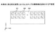
図1は、本発明に係る発光装置の概略構成を例示する平面図である。図2は、本発明に係る発光装置におけるLSIチップの概略構成を例示する平面図である。図3は、本発明に係る発光装置におけるLSIチップの概略構成を例示する断面図である。図4は、本発明に係る発光装置におけるLSIチップの概略構成を例示する平面図である。 FIG. 1 is a plan view illustrating a schematic configuration of a light-emitting device according to the present invention. FIG. 2 is a plan view illustrating a schematic configuration of an LSI chip in the light emitting device according to the invention. FIG. 3 is a cross-sectional view illustrating a schematic configuration of an LSI chip in the light emitting device according to the invention. FIG. 4 is a plan view illustrating a schematic configuration of an LSI chip in the light emitting device according to the invention.
発光装置は、図1に示すように、基板100と、基板100の表面に実装されたLSIチップ200とを有する。また、LSIチップ200は、後述する有機EL発光素子300が形成される有機EL発光領域Aを有する。 As shown in FIG. 1, the light emitting device includes a
基板100は、例えば図1のX方向を長軸方向とする矩形の形状とすることができる。また、基板100の表面に複数のLSIチップ200を長軸方向に沿って一列配置で実装することによって、有機EL発光素子300を用いた広い連続的な発光領域を得ることができる。基板100としては、高い封止性を備えることが好ましく、例えばガラス基板を好適に用いることができる。 The
LSIチップ200は、例えばダイボンド装置を用いて基板100の表面にダイボンド実装されている。ダイボンド装置を用いて基板100の表面にLSIチップ200をダイボンド実装する場合、高い位置精度、例えば±数μmの位置精度でLSIチップ200を基板100の表面にダイボンド実装することができる。 The
LSIチップ200における基板100と接合していない側の面(以下「LSIチップ200の表面」という。)には、図2に示すように、複数の第1の電極201が形成されている。複数の第1の電極201は、有機EL発光領域Aに形成されており、後述する有機EL発光素子300のアノード電極として機能する。 A plurality of
また、LSIチップ200は、後述するシリコンウエハ上に形成された有機EL発光素子300を駆動するための駆動回路、駆動回路を制御する制御回路等を含む。 The
駆動回路及び制御回路は、例えばトランジスタと、金属配線と、フィールド絶縁膜、層間絶縁膜、パッシベーション膜等の絶縁膜とによって形成されている。また、駆動回路は、第1の電極201と電気的に接続されている。そして、後述する複数の有機EL発光素子300を用いる発光装置においては、駆動回路及び制御回路によって、各々の有機EL発光素子300が独立して制御される。 The drive circuit and the control circuit are formed of, for example, a transistor, a metal wiring, and an insulating film such as a field insulating film, an interlayer insulating film, and a passivation film. In addition, the driver circuit is electrically connected to the
また、図3に示すように、LSIチップ200の表面(図3の+Z方向側の面)の端部に、LSIチップ200よりも外側に張り出した庇状の絶縁膜202が形成されていることが好ましい。これにより、LSIチップ200の第1の電極201上に後述する有機EL発光体301及び第2の電極302を形成したときに、LSIチップ200のシリコンウエハと第2の電極302とが短絡(ショート)することを回避することができる。 Further, as shown in FIG. 3, a hook-like
絶縁膜202としては、駆動回路、制御回路等を形成するときに用いられる、フィールド絶縁膜、層間絶縁膜、パッシベーション膜等の複数の絶縁膜のうちのいずれか一つ又はその組合せによって形成されていることが好ましい。これにより、別体で絶縁膜202を形成する必要がなく、LSIチップ200に含まれる回路を形成するときに用いられる装置を使用することができるため、新たな製造装置の開発をする必要がなくなり、導入コストを削減することができる。なお、絶縁膜202の形成方法については後述する。 The
有機EL発光素子300は、図4に示すように、LSIチップ200の有機EL発光領域Aに形成された第1の電極201上に形成されている。より具体的には、LSIチップ200の表面に形成された複数の第1の電極201の各々に対応するように、複数の有機EL発光素子300が形成されている。 As shown in FIG. 4, the organic EL
なお、図4においては、複数の有機EL発光素子300が図4のY方向に2列となるように形成されているが、本発明はこの点において限定されるものではなく、1列であってもよく、3列以上であってもよい。また、第1の電極201の形状及び配置位置並びに有機EL発光素子300の形状及び配置位置については特に限定されるものではなく、用途に応じて決定することができる。 In FIG. 4, the plurality of organic EL
有機EL発光素子300の具体的な構成例について、図5を参照しながら説明する。図5は、本発明に係る発光装置の概略構成を例示する断面図である。なお、説明の便宜上、図5は、図4で説明した複数の有機EL発光素子300のうちの一つを示している。 A specific configuration example of the organic EL
有機EL発光素子300は、基板100の表面に実装されたLSIチップ200の第1の電極201と、第1の電極201上に形成された有機EL発光体301、第2の電極302及び封止膜303とを有する。 The organic EL
また、有機EL発光素子300は、2つの電極(第1の電極201及び第2の電極302)によって、有機EL発光体301が挟み込まれた構成となっている。そして、図示しない外部電源等によって2つの電極間に電圧が印加されると、有機EL発光体301が発光する。 The organic EL
第1の電極201は、予めLSIチップ200に形成されている電極であり、有機EL発光素子300のアノード電極として機能する。 The
有機EL発光体301は、複数の膜、例えば正孔注入層3011、正孔輸送層3012、発光層3013、電子輸送層3014、電子注入層3015を含む。有機EL発光体301は、予め基板100の表面にダイボンド実装されたLSIチップ200の第1の電極201上に形成される。 The organic
有機EL発光体301の形成方法としては、予め基板100の表面にダイボンド実装されたLSIチップ200の第1の電極201上に有機EL発光体301を形成する方法であれば特に限定されるものではなく、真空蒸着法を好適に用いることができる。そして、真空蒸着法による蒸着のときにメタルマスクを用いることによって、所望の位置、例えば第1の電極201上に有機EL発光体301を形成することができる。 The method for forming the organic
また、真空蒸着法を用いて有機EL発光体301を形成することによって、LSIチップ200に含まれる回路を形成するときに用いられる装置を使用することができるため、新たな製造装置の開発をする必要がなくなり、導入コストを削減することができる。 Further, by forming the organic EL light-emitting
さらに、予め基板100の表面にダイボンド実装された複数のLSIチップ200に対して、同時に有機EL発光体301を成膜することができるため、複数のLSIチップ200間の有機EL発光素子300の直線性が確保できる。 Furthermore, since the organic EL
真空蒸着法の種類としては、特に限定されるものではなく、有機EL発光体301の材料、基板100の種類等に応じて選択することができ、例えば抵抗加熱蒸着法、電子ビーム蒸着法によって有機EL発光体301の材料を昇華(気化)させる方法が挙げられる。 The type of the vacuum deposition method is not particularly limited, and can be selected according to the material of the organic EL light-emitting
有機EL発光体301を構成する材料としては、特に限定されるものではないが、真空蒸着法を用いる場合には、真空蒸着法で成膜することが可能な材料を選択することができる。 The material constituting the organic EL light-emitting
第2の電極302は、有機EL発光体301上に形成されている電極であり、有機EL発光素子300のカソード電極として機能する。第2の電極302の形成方法としては、例えば真空蒸着法を用いることができる。 The
封止膜303は、例えば第1の電極201、有機EL発光体301及び第2の電極302が大気中の酸素と反応して劣化することを防止する膜である。封止膜303の形成方法としては、例えば真空蒸着法を用いることができる。 The sealing
以上に説明したように、本実施形態に係る発光装置によれば、LSIチップ200の第1の電極201上に複数の膜を含む有機EL発光体301と、第2の電極302とが形成されている。すなわち、LSIチップ200と有機EL発光素子300とが、ボンディングワイヤ、導電性接着剤等を用いることなく、電気的に直接接続されている。このため、LSIチップ200と有機EL発光素子300とを高い位置精度で接続することができる。また、LSIチップ200と有機EL発光素子300との接続に要するコストの削減、工程の簡素化及び基板の小型化を図ることができる。 As described above, according to the light emitting device according to the present embodiment, the organic EL
なお、図5では、正孔注入層3011、正孔輸送層3012、発光層3013、電子輸送層3014及び電子注入層3015からなる5層構造の有機EL発光体301について説明したが、本発明はこの点において限定されるものではない。 Note that FIG. 5 illustrates the organic EL light-emitting
有機EL発光体301としては、例えば正孔注入層3011、正孔輸送層3012、発光層3013及び電子注入層3015からなる4層構造であってもよい。この場合、発光層3013として電子輸送性を兼ね備える材料を選択することが好ましい。 The organic EL
また、有機EL発光体301としては、例えば正孔輸送層3012、発光層3013及び電子輸送層3014からなる3層構造であってもよい。この場合、正孔輸送層3012として正孔注入層3011の機能を兼ね備える材料を選択し、電子輸送層3014として電子注入層3015の機能を兼ね備える材料を選択することが好ましい。 In addition, the organic EL
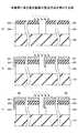
次に、LSIチップ200の表面の端部に、LSIチップ200よりも外側に張り出した庇状の絶縁膜202を形成する方法の一例について、図6を参照しながら説明する。図6は、本発明に係る発光装置におけるLSIチップの製造方法を例示する図である。なお、説明の便宜上、図6では、隣接する2つのLSIチップ200について示しているが、LSIチップの数は特に限定されるものではない。 Next, an example of a method of forming the hook-shaped insulating
LSIチップ200の表面の端部に位置し、LSIチップ200よりも外側に張り出した庇状の絶縁膜202は、LSIチップ200における絶縁膜202が形成されていない側の面(以下「LSIチップ200の裏面」という。)からLSIチップ200をフォトエッチングすることによって形成される。 An eaves-like insulating
以下、図6(a)から(e)を参照しながら具体的に説明する。 Hereinafter, a specific description will be given with reference to FIGS.
図6(a)は、シリコンウエハ上での隣接する2つのLSIチップ200間のダイシングラインDL近傍に絶縁膜202が形成されている状態を示している。絶縁膜202は、LSIチップ200の回路形成のときに用いられる、フィールド酸化膜、層間絶縁膜、パッシベーション膜等の複数の絶縁膜のうちのいずれか一つ又はその組合せによって形成されている。 FIG. 6A shows a state where an insulating
まず、図6(a)で示したLSIチップ200の裏面に酸化膜203を形成した後、酸化膜203上にレジスト膜204を塗布し、プリベークを行う。 First, after forming the
続いて、酸化膜203及びレジスト膜204が塗布されたLSIチップ200の裏面に、所望のパターンを有するフォトマスクを用いて紫外線を照射する。これにより、フォトマスクのパターンがレジスト膜204に転写(露光)される。 Subsequently, the back surface of the
続いて、純水洗浄によって露光された部分のレジスト膜204を除去する。これにより、図6(b)に示すように、シリコンウエハ上での隣接する2つのLSIチップ200間のダイシングラインDL近傍に塗布されたレジスト膜204が除去される。 Subsequently, the exposed resist
なお、所望のパターンとしては、ダイシングラインDLを挟んでダイシングラインDL近傍に形成された絶縁膜202間の距離L1よりも長い距離L2を有する開口部Hが形成されるパターンであることが好ましい。 The desired pattern is preferably a pattern in which an opening H having a distance L2 longer than the distance L1 between the insulating
続いて、ポストベークを行った後、図6(c)に示すように、LSIチップ200の裏面側からドライエッチングを行う(破線矢印参照)ことによって、レジスト膜204に覆われていない部分の酸化膜203を除去する。 Subsequently, after post-baking, as shown in FIG. 6C, dry etching is performed from the back side of the LSI chip 200 (see the broken line arrow) to oxidize a portion not covered with the resist
続いて、図6(d)に示すように、LSIチップ200の裏面側からドライエッチングを行う(破線矢印参照)ことによって、酸化膜203に覆われていない部分のLSIチップ200を除去する。このとき、絶縁膜202のエッチングレートがシリコンウエハのエッチングレートより小さくなるように、ドライエッチングを行う。これにより、絶縁膜202とLSIチップ200との間のエッチングレートの差によって、LSIチップ200の表面に形成された絶縁膜202はほとんどエッチングされることなく、LSIチップ200が優先的にエッチングされる。すなわち、絶縁膜202は、LSIチップ200の裏面側からのドライエッチングに対して、エッチングストップ層として機能する。このため、LSIチップ200の回路形成のときに用いられる装置を使用することができる。結果として、新たな製造装置の開発をする必要がなくなり、導入コストを削減することができる。 Subsequently, as shown in FIG. 6D, dry etching is performed from the back surface side of the LSI chip 200 (see the broken line arrow) to remove the
続いて、図6(e)に示すように、LSIチップ200の裏面に残ったレジスト膜204及び酸化膜203を除去する。これにより、複数のLSIチップ200が各々のLSIチップ200に切り出され(分離され)、LSIチップ200の表面の端部にLSIチップ200よりも外側に張り出した庇状の絶縁膜202が形成される。なお、LSIチップ200を分離するときに、ダイシングテープ等によってLSIチップ200の表面の保護及び固定を行うことが好ましい。 Subsequently, as shown in FIG. 6E, the resist
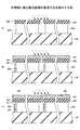
次に、LSIチップ200の表面の端部に、LSIチップ200よりも外側に張り出した庇状の絶縁膜202を形成する方法の他の例について、図7を参照しながら説明する。図7は、本発明に係る発光装置におけるLSIチップ200の製造方法を例示する図である。なお、説明の便宜上、図7では、隣接する2つのLSIチップ200について示しているが、LSIチップ200の数は特に限定されるものではない。 Next, another example of the method of forming the hook-shaped insulating
LSIチップ200の表面の端部に位置し、LSIチップ200よりも外側に張り出した庇状の絶縁膜202は、LSIチップ200の表面からLSIチップ200をドライエッチングすることによって形成される。 A hook-like
以下、図7(a)から(d)を参照しながら具体的に説明する。 Hereinafter, a specific description will be given with reference to FIGS.
図7(a)は、シリコンウエハ上での隣接する2つのLSIチップ200間のダイシングラインDL近傍に絶縁膜202が形成されている状態を示している。絶縁膜202は、LSIチップ200の回路形成のときに用いられる、フィールド酸化膜、層間絶縁膜、パッシベーション膜等の複数の絶縁膜のうちのいずれか一つ又はその組合せによって形成されている。 FIG. 7A shows a state where an insulating
まず、図7(b)に示すように、図7(a)で示したLSIチップ200の表面側からドライエッチングを行う(破線矢印参照)。このとき、絶縁膜202のエッチングレートがシリコンウエハのエッチングレートより小さくなるように、ドライエッチングを行う。これにより、図7(c)に示すように、絶縁膜202に覆われていない部分のLSIチップ200が除去される。 First, as shown in FIG. 7B, dry etching is performed from the surface side of the
ドライエッチングを更に行うと、絶縁膜202とLSIチップ200との間のエッチングレートの差によって、図7(d)に示すように、LSIチップ200の側壁部分が更にエッチングされる。また、深さ方向についてはダイシングした状態となるため、隣接する2つのLSIチップ200が分離される。これにより、LSIチップ200の表面の端部に、LSIチップ200よりも外側に張り出した庇状の絶縁膜202が形成される。 When dry etching is further performed, the side wall portion of the
なお、ドライエッチングにおいては、絶縁膜202とLSIチップ200との間のエッチングレートの差によって、LSIチップ200の表面に形成された絶縁膜202はほとんどエッチングされず、LSIチップ200の側壁部分が優先的にエッチングされる。このため、LSIチップ200の回路形成のときに用いられる装置を使用することができる。結果として、新たな製造装置の開発をする必要がなくなり、導入コストを削減することができる。 In dry etching, due to the difference in etching rate between the insulating
また、LSIチップ200を分離するときに、ダイシングテープ等によってLSIチップ200の表面の保護及び固定を行うことが好ましい。 Further, when separating the
以上、LSIチップ200の表面の端部に、LSIチップ200よりも外側に張り出した庇状の絶縁膜202を形成する方法について、図6及び図7を参照しながら説明したが、本発明はこの点において限定されるものではない。 As described above, the method of forming the hook-shaped insulating
次に、基板100の表面に実装されたLSIチップ200上に有機EL発光体301及び第2の電極302を形成する方法について、図8及び図9を参照しながら説明する。 Next, a method for forming the organic EL
図8及び図9は、本発明に係る発光装置の製造方法を例示する図である。なお、図8及び図9における破線矢印は、有機EL発光体301又は第2の電極302が蒸着される状態を簡易的に表す。また、説明の便宜上、図8及び図9では、隣接する2つのLSIチップ200について示しているが、LSIチップ200の数は特に限定されるものではない。 8 and 9 are views illustrating a method for manufacturing a light-emitting device according to the present invention. 8 and 9 simply indicate a state in which the organic EL
図8(a)は、LSIチップ200の表面の端部に、LSIチップ200よりも外側に張り出した庇状の絶縁膜202を有していない場合のLSIチップ200を基板100の表面に複数個実装した状態を示している。 FIG. 8A shows a plurality of
まず、図8(a)に示した基板100の表面に実装されたLSIチップ200上に、真空蒸着法により、有機EL発光体301を成膜する(図8(b))。 First, an organic EL light-emitting
続いて、真空蒸着法により、有機EL発光体301上に第2の電極302を成膜する(図8(c))。 Subsequently, a
以上の工程により、基板100の表面に実装されたLSIチップ200上に有機EL発光体301及び第2の電極302を形成することができる。 Through the above steps, the organic EL
すなわち、LSIチップ200と有機EL発光素子300とが、ボンディングワイヤ、導電性接着剤等を用いることなく、電気的に直接接続されている。このため、LSIチップ200と有機EL発光素子300とを高い位置精度で接続することができる。また、LSIチップ200と有機EL発光素子300との接続に要するコストの削減、工程の簡素化及び基板の小型化を図ることができる。 That is, the
ところで、LSIチップ200上に有機EL発光体301及び第2の電極302を形成する場合、有機EL発光体301及び第2の電極は、図8(c)に示すように、絶縁膜202の表及び側壁面、LSIチップ200の側壁面等に付着することがある。 Incidentally, when the organic EL
係る場合、有機EL発光体301は高抵抗な膜から構成されているため、LSIチップ200の側壁面等に付着した場合であっても、有機EL発光素子300の特性への影響はほとんどない。しかしながら、第2の電極302は金属であるため、LSIチップ200の側壁面に付着すると、第2の電極302とLSIチップ200のシリコンウエハとの間が短絡状態となる可能性がある。 In such a case, since the organic EL light-emitting
そこで、図9に示すように、LSIチップ200の表面の端部に、LSIチップ200よりも外側に張り出した庇状の絶縁膜202が形成されていることが好ましい。 Therefore, as shown in FIG. 9, it is preferable that a hook-shaped insulating
図9(a)は、LSIチップ200の表面の端部に、LSIチップ200よりも外側に張り出した庇状の絶縁膜202を有する場合のLSIチップ200を基板100の表面に複数個実装した状態を示している。 FIG. 9A shows a state in which a plurality of
まず、図9(a)に示した基板100の表面に実装されたLSIチップ200上に、真空蒸着法により、有機EL発光体301を成膜する(図9(b))。 First, an organic EL light-emitting
続いて、真空蒸着法により、有機EL発光体301上に第2の電極302を成膜する(図9(c))。 Subsequently, the
以上の工程により、基板100の表面に実装されたLSIチップ200上に有機EL発光体301及び第2の電極302を形成することができる。 Through the above steps, the organic EL
ここで、有機EL発光体301及び第2の電極302は、図9(c)に示すように、絶縁膜202の表面及び側壁面、LSIチップ200の側壁面等に付着することがある。 Here, as shown in FIG. 9C, the organic EL
しかしながら、LSIチップ200の表面の端部に、LSIチップ200よりも外側に張り出した庇状の絶縁膜202が形成されているため、有機EL発光体301及び第2の電極302は、庇状の絶縁膜202の裏面側に付着することはない。このため、絶縁膜202の表面及び側壁面に形成された有機EL発光体301及び第2の電極302と、LSIチップ200の側壁面に付着した有機EL発光体301及び第2の電極302とは、連続して形成されることなく、途切れた状態となる。結果として、第2の電極302とLSIチップ200との間で電流リークが発生することを抑制することができ、有機EL発光素子300の特性への影響を抑制することができる。 However, since the hook-shaped insulating
以上、発光装置を実施形態により説明したが、本発明は上記実施形態に限定されるものではなく、本発明の範囲内で種々の変形及び改良が可能である。 The light emitting device has been described above by way of the embodiment, but the present invention is not limited to the above embodiment, and various modifications and improvements can be made within the scope of the present invention.
100 基板
200 LSIチップ
201 第1の電極
202 絶縁膜
301 有機EL発光体
3011 正孔注入層
3012 正孔輸送層
3013 発光層
3014 電子輸送層
3015 電子注入層
302 第2の電極100
Claims (7)
Translated fromJapanese前記第1の電極上に形成され、複数の膜を含む有機EL発光体と、
前記有機EL発光体上に形成された第2の電極と
を含む発光装置。An LSI chip mounted on the surface of the substrate and including a first electrode;
An organic EL light emitter formed on the first electrode and including a plurality of films;
And a second electrode formed on the organic EL light emitter.
請求項1に記載の発光装置。The plurality of films are formed by a vacuum evaporation method.
The light emitting device according to claim 1.
請求項1又は2に記載の発光装置。A hook-shaped insulating film projecting outward from the LSI chip is formed at an end of the surface of the LSI chip where the organic EL light emitting body is formed.
The light emitting device according to claim 1.
請求項3に記載の発光装置。The insulating film is formed of any one of a plurality of insulating films constituting the LSI chip or a combination thereof.
The light emitting device according to claim 3.
ドライエッチングにより前記シリコンウエハと前記絶縁膜との間のエッチングレートの差によって、前記複数のLSIチップを分離するとともに前記絶縁膜を庇状に形成する工程と、
前記LSIチップを基板の表面に実装する工程と、
前記LSIチップの前記第1の電極上に複数の膜を含む有機EL発光体を形成する工程と、
前記有機EL発光体上に第2の電極を形成する工程と
を含む発光装置の製造方法。Forming a plurality of LSI chips including a first electrode and an insulating film on a silicon wafer;
Separating the plurality of LSI chips according to a difference in etching rate between the silicon wafer and the insulating film by dry etching, and forming the insulating film in a bowl shape;
Mounting the LSI chip on the surface of the substrate;
Forming an organic EL light emitter including a plurality of films on the first electrode of the LSI chip;
Forming a second electrode on the organic EL light-emitting body.
前記絶縁膜のエッチングレートは前記シリコンウエハのエッチングレートより小さい、
請求項5に記載の発光装置の製造方法。The step of separating the plurality of LSI chips and forming the insulating film in a bowl shape includes the step of dry etching the LSI chip from the surface of the LSI chip where the insulating film is not formed,
The etching rate of the insulating film is smaller than the etching rate of the silicon wafer,
The manufacturing method of the light-emitting device of Claim 5.
前記絶縁膜のエッチングレートは前記シリコンウエハのエッチングレートより小さい、
請求項5に記載の発光装置の製造方法。The step of separating the plurality of LSI chips and forming the insulating film in a bowl shape includes the step of dry etching the LSI chip from the surface of the LSI chip on which the insulating film is formed,
The etching rate of the insulating film is smaller than the etching rate of the silicon wafer,
The manufacturing method of the light-emitting device of Claim 5.
Priority Applications (1)
| Application Number | Priority Date | Filing Date | Title |
|---|---|---|---|
| JP2014162878AJP2016039318A (en) | 2014-08-08 | 2014-08-08 | Light-emitting device and manufacturing method of the same |
Applications Claiming Priority (1)
| Application Number | Priority Date | Filing Date | Title |
|---|---|---|---|
| JP2014162878AJP2016039318A (en) | 2014-08-08 | 2014-08-08 | Light-emitting device and manufacturing method of the same |
Publications (1)
| Publication Number | Publication Date |
|---|---|
| JP2016039318Atrue JP2016039318A (en) | 2016-03-22 |
Family
ID=55530138
Family Applications (1)
| Application Number | Title | Priority Date | Filing Date |
|---|---|---|---|
| JP2014162878APendingJP2016039318A (en) | 2014-08-08 | 2014-08-08 | Light-emitting device and manufacturing method of the same |
Country Status (1)
| Country | Link |
|---|---|
| JP (1) | JP2016039318A (en) |
- 2014
- 2014-08-08JPJP2014162878Apatent/JP2016039318A/enactivePending
Similar Documents
| Publication | Publication Date | Title |
|---|---|---|
| CN107408606B (en) | light emitting element, light emitting unit, light emitting panel device, and method of driving light emitting panel device | |
| CN110034149A (en) | LED device | |
| KR101873259B1 (en) | Method for manufacturing micro-array light emitting diode and apparatus for lighting | |
| US9774001B2 (en) | Display device and method for manufacturing display device | |
| JP2008235248A (en) | Display substrate, organic light emitting diode display device including the same, and manufacturing method thereof | |
| CN100416889C (en) | flat panel display device | |
| CN103730478A (en) | Semiconductor light emitting device | |
| JP6555907B2 (en) | Semiconductor light emitting device | |
| JP7132779B2 (en) | Display device and array substrate | |
| CN110178220B (en) | Method for producing an optoelectronic semiconductor component and optoelectronic semiconductor component | |
| CN104037362A (en) | Method for manufacturing display element, display element, and display device | |
| JP4871978B2 (en) | Semiconductor device and optical print head | |
| KR20210022726A (en) | Optoelectronic device with light emitting diode | |
| CN103098215A (en) | Organic electroluminescent device | |
| JP6409287B2 (en) | ORGANIC ELECTROLUMINESCENCE LIGHT EMITTING DEVICE, ORGANIC ELECTROLUMINESCENCE LIGHT EMITTING DEVICE MANUFACTURING METHOD, AND IMAGE FORMING DEVICE | |
| US9196854B2 (en) | Organic EL lighting emitting device, method of manufacturing the same, and organic EL light source device | |
| CN101257057B (en) | semiconductor light device | |
| US20240163984A1 (en) | Light emitting device | |
| CN111902855A (en) | Method for manufacturing display device and display device | |
| JP2016039318A (en) | Light-emitting device and manufacturing method of the same | |
| JP5313769B2 (en) | Multilayer substrate and light emitting device manufacturing method | |
| WO2020202274A1 (en) | Display device, and method for manufacturing display device | |
| CN116387226A (en) | Transfer substrate and preparation method thereof, display device and transfer method of light-emitting element | |
| JP7091598B2 (en) | Manufacturing method of light emitting device | |
| JP2014225356A (en) | Light-emitting element |