JP2016038434A - Liquid crystal display device - Google Patents
Liquid crystal display deviceDownload PDFInfo
- Publication number
- JP2016038434A JP2016038434AJP2014160415AJP2014160415AJP2016038434AJP 2016038434 AJP2016038434 AJP 2016038434AJP 2014160415 AJP2014160415 AJP 2014160415AJP 2014160415 AJP2014160415 AJP 2014160415AJP 2016038434 AJP2016038434 AJP 2016038434A
- Authority
- JP
- Japan
- Prior art keywords
- liquid crystal
- crystal display
- display device
- organic passivation
- passivation film
- Prior art date
- Legal status (The legal status is an assumption and is not a legal conclusion. Google has not performed a legal analysis and makes no representation as to the accuracy of the status listed.)
- Pending
Links
Images


Classifications
- G—PHYSICS
- G02—OPTICS
- G02F—OPTICAL DEVICES OR ARRANGEMENTS FOR THE CONTROL OF LIGHT BY MODIFICATION OF THE OPTICAL PROPERTIES OF THE MEDIA OF THE ELEMENTS INVOLVED THEREIN; NON-LINEAR OPTICS; FREQUENCY-CHANGING OF LIGHT; OPTICAL LOGIC ELEMENTS; OPTICAL ANALOGUE/DIGITAL CONVERTERS
- G02F1/00—Devices or arrangements for the control of the intensity, colour, phase, polarisation or direction of light arriving from an independent light source, e.g. switching, gating or modulating; Non-linear optics
- G02F1/01—Devices or arrangements for the control of the intensity, colour, phase, polarisation or direction of light arriving from an independent light source, e.g. switching, gating or modulating; Non-linear optics for the control of the intensity, phase, polarisation or colour
- G02F1/13—Devices or arrangements for the control of the intensity, colour, phase, polarisation or direction of light arriving from an independent light source, e.g. switching, gating or modulating; Non-linear optics for the control of the intensity, phase, polarisation or colour based on liquid crystals, e.g. single liquid crystal display cells
- G02F1/133—Constructional arrangements; Operation of liquid crystal cells; Circuit arrangements
- G02F1/1333—Constructional arrangements; Manufacturing methods
- G02F1/1339—Gaskets; Spacers; Sealing of cells
- G—PHYSICS
- G02—OPTICS
- G02F—OPTICAL DEVICES OR ARRANGEMENTS FOR THE CONTROL OF LIGHT BY MODIFICATION OF THE OPTICAL PROPERTIES OF THE MEDIA OF THE ELEMENTS INVOLVED THEREIN; NON-LINEAR OPTICS; FREQUENCY-CHANGING OF LIGHT; OPTICAL LOGIC ELEMENTS; OPTICAL ANALOGUE/DIGITAL CONVERTERS
- G02F1/00—Devices or arrangements for the control of the intensity, colour, phase, polarisation or direction of light arriving from an independent light source, e.g. switching, gating or modulating; Non-linear optics
- G02F1/01—Devices or arrangements for the control of the intensity, colour, phase, polarisation or direction of light arriving from an independent light source, e.g. switching, gating or modulating; Non-linear optics for the control of the intensity, phase, polarisation or colour
- G02F1/13—Devices or arrangements for the control of the intensity, colour, phase, polarisation or direction of light arriving from an independent light source, e.g. switching, gating or modulating; Non-linear optics for the control of the intensity, phase, polarisation or colour based on liquid crystals, e.g. single liquid crystal display cells
- G02F1/133—Constructional arrangements; Operation of liquid crystal cells; Circuit arrangements
- G02F1/136—Liquid crystal cells structurally associated with a semi-conducting layer or substrate, e.g. cells forming part of an integrated circuit
- G02F1/1362—Active matrix addressed cells
- G02F1/1368—Active matrix addressed cells in which the switching element is a three-electrode device
- G—PHYSICS
- G02—OPTICS
- G02F—OPTICAL DEVICES OR ARRANGEMENTS FOR THE CONTROL OF LIGHT BY MODIFICATION OF THE OPTICAL PROPERTIES OF THE MEDIA OF THE ELEMENTS INVOLVED THEREIN; NON-LINEAR OPTICS; FREQUENCY-CHANGING OF LIGHT; OPTICAL LOGIC ELEMENTS; OPTICAL ANALOGUE/DIGITAL CONVERTERS
- G02F1/00—Devices or arrangements for the control of the intensity, colour, phase, polarisation or direction of light arriving from an independent light source, e.g. switching, gating or modulating; Non-linear optics
- G02F1/01—Devices or arrangements for the control of the intensity, colour, phase, polarisation or direction of light arriving from an independent light source, e.g. switching, gating or modulating; Non-linear optics for the control of the intensity, phase, polarisation or colour
- G02F1/13—Devices or arrangements for the control of the intensity, colour, phase, polarisation or direction of light arriving from an independent light source, e.g. switching, gating or modulating; Non-linear optics for the control of the intensity, phase, polarisation or colour based on liquid crystals, e.g. single liquid crystal display cells
- G02F1/133—Constructional arrangements; Operation of liquid crystal cells; Circuit arrangements
- G02F1/1333—Constructional arrangements; Manufacturing methods
- G02F1/133308—Support structures for LCD panels, e.g. frames or bezels
- G02F1/133311—Environmental protection, e.g. against dust or humidity
- G—PHYSICS
- G02—OPTICS
- G02F—OPTICAL DEVICES OR ARRANGEMENTS FOR THE CONTROL OF LIGHT BY MODIFICATION OF THE OPTICAL PROPERTIES OF THE MEDIA OF THE ELEMENTS INVOLVED THEREIN; NON-LINEAR OPTICS; FREQUENCY-CHANGING OF LIGHT; OPTICAL LOGIC ELEMENTS; OPTICAL ANALOGUE/DIGITAL CONVERTERS
- G02F1/00—Devices or arrangements for the control of the intensity, colour, phase, polarisation or direction of light arriving from an independent light source, e.g. switching, gating or modulating; Non-linear optics
- G02F1/01—Devices or arrangements for the control of the intensity, colour, phase, polarisation or direction of light arriving from an independent light source, e.g. switching, gating or modulating; Non-linear optics for the control of the intensity, phase, polarisation or colour
- G02F1/13—Devices or arrangements for the control of the intensity, colour, phase, polarisation or direction of light arriving from an independent light source, e.g. switching, gating or modulating; Non-linear optics for the control of the intensity, phase, polarisation or colour based on liquid crystals, e.g. single liquid crystal display cells
- G02F1/133—Constructional arrangements; Operation of liquid crystal cells; Circuit arrangements
- G02F1/1333—Constructional arrangements; Manufacturing methods
- G02F1/133345—Insulating layers
- G—PHYSICS
- G02—OPTICS
- G02F—OPTICAL DEVICES OR ARRANGEMENTS FOR THE CONTROL OF LIGHT BY MODIFICATION OF THE OPTICAL PROPERTIES OF THE MEDIA OF THE ELEMENTS INVOLVED THEREIN; NON-LINEAR OPTICS; FREQUENCY-CHANGING OF LIGHT; OPTICAL LOGIC ELEMENTS; OPTICAL ANALOGUE/DIGITAL CONVERTERS
- G02F1/00—Devices or arrangements for the control of the intensity, colour, phase, polarisation or direction of light arriving from an independent light source, e.g. switching, gating or modulating; Non-linear optics
- G02F1/01—Devices or arrangements for the control of the intensity, colour, phase, polarisation or direction of light arriving from an independent light source, e.g. switching, gating or modulating; Non-linear optics for the control of the intensity, phase, polarisation or colour
- G02F1/13—Devices or arrangements for the control of the intensity, colour, phase, polarisation or direction of light arriving from an independent light source, e.g. switching, gating or modulating; Non-linear optics for the control of the intensity, phase, polarisation or colour based on liquid crystals, e.g. single liquid crystal display cells
- G02F1/133—Constructional arrangements; Operation of liquid crystal cells; Circuit arrangements
- G02F1/1333—Constructional arrangements; Manufacturing methods
- G02F1/1339—Gaskets; Spacers; Sealing of cells
- G02F1/13396—Spacers having different sizes
Landscapes
- Physics & Mathematics (AREA)
- Nonlinear Science (AREA)
- Mathematical Physics (AREA)
- Chemical & Material Sciences (AREA)
- Crystallography & Structural Chemistry (AREA)
- General Physics & Mathematics (AREA)
- Optics & Photonics (AREA)
- Engineering & Computer Science (AREA)
- Microelectronics & Electronic Packaging (AREA)
- Liquid Crystal (AREA)
- Devices For Indicating Variable Information By Combining Individual Elements (AREA)
Abstract
Translated fromJapaneseDescription
Translated fromJapanese本発明は表示装置に係り、表示領域に発生する黒むらを防止した液晶表示装置に関する。 The present invention relates to a display device, and more particularly to a liquid crystal display device which prevents black unevenness generated in a display area.
液晶表示装置では画素電極および薄膜トランジスタ(TFT)等を有する画素がマトリクス状に形成されたTFT基板と、TFT基板に対向して対向基板が配置され、TFT基板と対向基板の間に液晶が挟持されている構成となっている。そして液晶分子による光の透過率を画素毎に制御することによって画像を形成している。 In a liquid crystal display device, a TFT substrate in which pixels having pixel electrodes and thin film transistors (TFTs) are formed in a matrix and a counter substrate are arranged opposite the TFT substrate, and liquid crystal is sandwiched between the TFT substrate and the counter substrate. It has become the composition. An image is formed by controlling the light transmittance of the liquid crystal molecules for each pixel.
液晶表示装置において、表示領域の特に周辺部に黒いむらが発生することがある。これは、液晶内に侵入した水分の影響であると考えられる。水分が内部に侵入しないようにするために、種々の構造が開発されている。一方、内部に侵入した水分を吸着して、液晶表示装置内に水分が侵入しても、液晶への影響を小さく抑える方法も存在する。 In the liquid crystal display device, black unevenness may occur particularly in the peripheral portion of the display area. This is considered to be due to the influence of moisture that has entered the liquid crystal. Various structures have been developed to prevent moisture from entering the interior. On the other hand, there is a method in which moisture that has entered inside is adsorbed and the influence on the liquid crystal is suppressed even if moisture enters the liquid crystal display device.
特許文献1には、TFT基板と対向基板をシールするシール部に水分を吸着する吸湿層を配置する構成が記載されている。特許文献2には、表示領域とシール部の間に水分を吸着する吸湿層を配置する構成が記載されている。
特許文献1に記載の構成も特許文献2に記載の構成も液晶表示装置内に侵入した水分を吸着する吸着層を配置するものであるが、吸着層として、液晶表示装置に通常は使用されてない材料を用いるものである。つまり、液晶表示装置の動作として不可欠な材料以外のものを別部品として用いるものである。このような従来の方法は、次のような問題点を生ずる。 Both the configuration described in
(1)別部品を別工程によって配置するので、部品コストと工程増加による製造コストが増加する。(2)液晶表示装置の動作として不可欠な材料以外の材料を使用するので、長期間液晶表示装置を動作させた場合に、表示性能に影響が生じないか否かを確認する必要がある。 (1) Since the separate parts are arranged in separate processes, the part costs and the manufacturing costs due to the increased processes increase. (2) Since materials other than materials indispensable for the operation of the liquid crystal display device are used, it is necessary to confirm whether or not the display performance is affected when the liquid crystal display device is operated for a long period of time.
本発明の課題は、上記のような問題点を克服し、製造コストの増加無しに、あるいは、信頼性の低下をきたすことなく、液晶表示パネル内に侵入した水分を効果的に吸着し、液晶表示装置における黒むらの発生を防止することである。 An object of the present invention is to overcome the above-described problems and effectively adsorb moisture that has entered the liquid crystal display panel without increasing the manufacturing cost or reducing the reliability. This is to prevent black unevenness in the display device.
本発明は上記問題を克服するものであり、具体的な手段は次のとおりである。 The present invention overcomes the above problems, and specific means are as follows.
(1)表示領域と端子部を有し、有機パッシベーション膜が形成されたTFT基板と、対向基板が、シール部おいて接着し、内部に液晶が封入された液晶表示装置であって、前記TFT基板の前記シール部には、前記有機パッシベーション膜に、前記表示領域を囲むように、溝状スルーホールが形成され、前記溝状スルーホールの内部には、前記有機パッシベーション膜と同じ材料で形成され、前記有機パッシベーション膜と同じ工程で形成された水分吸収層が形成され、前記水分吸収層は無機絶縁膜によって覆われていないことを特徴とする液晶表示装置。 (1) A liquid crystal display device in which a TFT substrate having a display region and a terminal portion, on which an organic passivation film is formed, and a counter substrate are bonded together at a seal portion and liquid crystal is enclosed therein, and the TFT In the seal portion of the substrate, a groove-like through hole is formed in the organic passivation film so as to surround the display region, and the groove-like through hole is formed of the same material as the organic passivation film. A liquid crystal display device, wherein a moisture absorption layer formed in the same process as the organic passivation film is formed, and the moisture absorption layer is not covered with an inorganic insulating film.
(2)前記水分吸収層は、前記表示領域を囲むように、全周に連続して形成されていることを特徴とする(1)に記載の液晶表示装置。 (2) The liquid crystal display device according to (1), wherein the moisture absorption layer is formed continuously around the entire circumference so as to surround the display area.
(3)前記水分吸収層は、前記表示領域を囲むように不連続に形成されていることを特徴とする(1)に記載の液晶表示装置。 (3) The liquid crystal display device according to (1), wherein the moisture absorption layer is formed discontinuously so as to surround the display region.
(4)前記水分吸収層は、前記表示領域のコーナー部のみに形成されていることを特徴とする(1)に記載の液晶表示装置。 (4) The liquid crystal display device according to (1), wherein the moisture absorption layer is formed only in a corner portion of the display region.
本発明の実施例を説明する前に、本発明と併用される、水分が液晶層に浸入しないようにした構成を説明する。図9は、液晶表示装置のシール部付近の断面図である。図9において、TFT基板100と対向基板200がシール材20によって接着している。TFT基板100の上には、平坦化膜を兼ねた有機パッシベーション膜4が形成されている。この有機パッシベーション膜104はアクリル樹脂等で形成されるので、水分を吸収し、かつ透過させやすい。また、有機パッシベーション膜104は平坦化膜を兼ねているので、1乃至4μm、通常は2μm乃至3μm程度と、厚く形成されるので、水分を透過させやすい。 Before describing the embodiments of the present invention, a configuration that is used in combination with the present invention so that moisture does not enter the liquid crystal layer will be described. FIG. 9 is a cross-sectional view of the vicinity of the seal portion of the liquid crystal display device. In FIG. 9, the
そこで、有機パッシベーション膜に、TFT基板100の端部に沿い、表示領域を囲むようにして溝状のスルーホールを形成している。基板端部から有機パッシベーション膜104に吸収され、内部に侵入して来た水分は、溝状スルーホール1041において、遮断され、液晶層300までは、到達しない。溝状スルーホール1041において、有機パッシベーション膜104はSiNで形成された絶縁膜105によって覆われているので、侵入した水分が溝状スルーホール1041を通過するには、長時間かかるので、その分、液晶表示装置の寿命が延びることになる。 Therefore, a groove-shaped through hole is formed in the organic passivation film along the end of the
しかし、図9のような構成は、水分が絶縁膜105を通過すると、その後は、水分は容易に液晶層300に到達する。したがって、図9のような構成では、液晶表示装置の長寿命化は限界がある。 However, in the configuration shown in FIG. 9, when moisture passes through the
なお、図9における対向基板200において、ブラックマトリクス201が基板の端部まで形成されている。ブラックマトリクス201は有機材料で形成される場合が多い。ブラックマトリクスが有機材料で形成される場合は、水分が端部から浸入し易い。ブラックマトリクス201を通して侵入してきた水分を遮断するために、ブラックマトリクス溝2011が形成されている。ブラックマトリクスはTFT基板100における有機パッシベーション膜104ほどは厚くないので、その分水分の浸入量もTFT基板側よりも小さい。以下に実施例を用いて本発明の内容を詳細に説明する。 In the
図1は本発明が適用される液晶表示装置の平面図である。図1において、TFT基板100と対向基板200がシール材20によって接着し、TFT基板100と対向基板200の間に液晶が挟持されている。TFT基板100は対向基板200よりも大きく形成されており、TFT基板100が1枚となっている部分は端子部150となっている。端子部150には、液晶表示パネルを駆動するICドライバ160、液晶表示パネルに、電源、映像信号、走査信号等を供給するためのフレキシブル配線基板を接続するための端子等が形成されている。 FIG. 1 is a plan view of a liquid crystal display device to which the present invention is applied. In FIG. 1, the
図1において、表示領域500には走査線30が横方向に延在し、縦方向に配列している。また、映像信号線40が縦方向に延在し、横方向に配列している。走査線30と映像信号線40とで囲まれた領域が画素35となっている。狭額縁では、表示領域500の端部と液晶表示装置の端部の距離wは1mm程度にまで小さくなっている。そうすると、シール材の幅も小さくなるが、シール材の幅が小さくなると、外部の水分が表示領域の液晶層に到達しやすくなる。そうすると、水分の影響による、いわゆる黒むらが発生しやすくなる。 In FIG. 1,
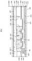
図2は、図1のA−A断面に相当するシール部の詳細断面図である。図2に示すシール部において、シール材20によってTFT基板100と対向基板200が接着している。図2において、シール材20の内側には液晶300が充填されている。
図2において、ガラスで形成されたTFT基板100に第1の絶縁膜101が形成されている。第1の絶縁膜101はガラスからの不純物がTFTの半導体層を汚染することを防止するために形成されるアンダーコート膜である場合もある。第1の絶縁膜101の上に第2の絶縁膜102が形成されている。第2の絶縁膜102は、TFTにおけるゲート絶縁膜である場合もある。第2の絶縁膜102の上に走査線引出し線103が形成されている。矩形の走査線引き出し線103は、図1における、図面の上側からの走査線引出し線103の断面である。FIG. 2 is a detailed cross-sectional view of a seal portion corresponding to the AA cross section of FIG. In the seal portion shown in FIG. 2, the
In FIG. 2, a first
走査線引出し線103を覆って有機パッシベーション膜104が形成されている。有機パッシベーション膜104は2乃至3μmと、厚く形成され、平坦化膜としての役割も有している。有機パッシベーション膜104は感光性樹脂で形成され、パターニングにフォトレジストを必要としない。 An
表示領域においては、有機パッシベーション膜104の上に形成される画素電極あるいはコモン電極とTFTのソース電極とを接続する必要があるが、この接続は有機パッシベーション膜104に形成されたスルーホールを介して行われる。有機パッシベーション膜104は、アクリル等の樹脂によって形成されている。このような膜は水分を吸収しやすいので、有機パッシベーション膜104の上に直接画素電極あるいはコモン電極を形成すると、有機パッシベーション膜104に吸収された水分の影響で、特にスルーホール部において、画素電極あるいはコモン電極等の剥がれが生ずる。このような現象を防止するために、従来は、スルーホールの径を大きくして、スルーホールにおいても、無機絶縁膜105が有機パッシベーション膜を確実に覆うように設計されていた。すなわち、有機パッシベーション膜104を無機絶縁膜105で覆うことは、従来は必須であると考えられてきた。 In the display region, it is necessary to connect the pixel electrode or common electrode formed on the
図2において、有機パッシベーション膜104の上にSiNで形成された層間絶縁膜105が形成されている。この層間絶縁膜105は、IPS方式の液晶表示装置の表示領域において、平面べたで形成された下層電極とスリットを有する上層電極の層間の絶縁膜である。下層電極がコモン電極で、上層電極が画素電極である場合もあるし、その逆の場合もあるが、下層電極も上層電極もITO(Indium Tin Oxide)で代表される透明酸化物導電膜で形成されている。 In FIG. 2, an
有機パッシベーション膜104は、水分を透過しやすいので、図9で説明したように、端部から有機パッシベーション膜104を透過してくる水分を遮断するために、有機パッシベーション膜104に溝状スルーホール1041が形成されている。この溝状スルーホール1041は、シール部内に表示領域を囲むように、TFT基板100の全周に形成される。 Since the
本発明の特徴は、この溝状スルーホール1041の内部に無機絶縁物で覆われない、有機パッシベーション膜によって形成された水分吸収層10を壁状に形成していることである。この水分吸収層10の存在は、TFT基板100の端部から有機パッシベーション膜104を透過してきた水分が、有機パッシベーション膜104の溝1041をさらに通過しょうとする場合、この水分を吸収する役割を有する。これによって、水分が液晶表示パネルの内部に侵入して、液晶層300に到達するまでの時間を長くすることができる。したがって、液晶表示装置の寿命を長くすることができる。 A feature of the present invention is that the
図2において、層間絶縁膜105の上に配向膜106が形成されている。配向膜106は、当初液体である配向膜材料を、フレキソ印刷、インクジェット等によって塗布するが、配向膜材料がシール部の外側端部にまで達しないように、ストッパーとして、有機パッシベーション膜104に凹部が3箇所形成されている。そして、凹部のさらに外側に形成されている溝状スルーホール1041も配向膜材料に対するストッパーの役割を有する。図2においては、配向膜材料は3個ある凹部を乗り越えて、最後の凸部において止まっている。 In FIG. 2, an
図2において、対向基板200側にはブラックマトリクス201が形成されている。図2におけるブラックマトリクス201はシール部からの光漏れを防止するために設けられている。ブラックマトリクス201は樹脂で形成されているので、樹脂を浸透してくる水分を遮断するためにブラックマトリクス溝2011が形成されている。ブラックマトリクス201の上には、カラーフィルタ202が紙面垂直方向にストライプ状に形成されている。カラーフィルタ202はオーバーコート膜203の上に形成される第1柱状スペーサ210に対応して形成されている。 In FIG. 2, a
カラーフィルタ202の上にオーバーコート膜203が形成されている。オーバーコート膜203には、カラーフィルタ202の部分に対応して凸部が形成されている。この凸部は、配向膜材料を塗布した時に配向膜材料が基板外側方向に広がろうとするのを防止する役割を有する。オーバーコート膜203の凸部に第1柱状スペーサ210が形成されている、第1柱状スペーサ210はシール部における対向基板200とTFT基板100の間隔を規定する役割を有する。 An
図2において、第1柱状スペーサ210よりも表示領域側に、第1柱状スペーサ210よりも高さが低い第2柱状スペーサ220が形成されている。第2柱状スペーサ220は対向基板200に外部から圧力が加わった場合、TFT基板100と対向基板200の間隔が過度に小さくなることを防止する役割を有する。 In FIG. 2, a second
第1柱状スペーサの外側には壁状スペーサ250が形成されている。この壁状スペーサは、配向膜に対するストッパーとなっている。壁状スペーサ250は2段形成されている。オーバーコート膜203を覆って配向膜105が形成されている。この配向膜は、壁状スペーサ250によって外形が区切られている。 A
シール部の端部には土手状スペーサ230が形成されている。液晶表示パネルは個々に製造すると効率が悪いので、マザー基板に複数の液晶表示パネルを形成し、複数の液晶表示パネルを一括して製造する。液晶表示パネルが複数形成されたマザー基板において、隣接する液晶表示パネルの境界に配置され、土手状スペーサ230の中心に沿ってスクライビングをいれ、その後、破断することによって個々の液晶表示パネルを分離する。土手状スペーサ230が無い場合、この部分はシール材20となるが、シール材20が存在すると、スクライビングを入れても破断が出来ない。 A bank-
図3は図2に対応する部分の平面図である。図3において、土手状スペーサ230の内側にシール材20が形成されている。図3において、カラーフィルタ202がストライプ状に形成され、カラーフィルタ202に対応する部分に第1柱状スペーサ210が配置している。図3では、カラーフィルタ202と第1柱状スペーサ210は2列分記載されている。第1柱状スペーサ210と第1柱状スペーサ210の間には壁状スペーサ250が配置している。シール材20は土手状スペーサ230の端部にまで形成されている。図3において、土手状スペーサ230とカラーフィルタ202の間に、TFT基板側において水分吸収層10が形成されている。 FIG. 3 is a plan view of a portion corresponding to FIG. In FIG. 3, the sealing
図4は、図2における水分吸収層10の部分を拡大した断面図である。図4において、有機パッシベーション膜104の溝状スルーホール1041の部分に水分吸収層10が形成されている。この水分吸収層10は、有機パッシベーション膜104と同じ材料で、同じ工程で形成されるので、水分吸収層を形成するために、追加の材料費も工程も発生しない。 4 is an enlarged cross-sectional view of a portion of the
水分吸収層10は、他の部分の有機パッシベーション膜104とは異なり、無機絶縁膜105には覆われていない。したがって、液晶表示装置が完成後、シール材20を伝わってきた水分を吸収することができる。図4において、水分吸収層10の幅w1は例えば30μmで、高さhは、2乃至3μmである。一方、有機パッシベーション膜204に形成された溝状スルーホール1041の幅は70μm程度である。但し、これらの数値は、水分吸収層によって期待する水分吸収効果に応じて調節することが出来る。図5は水分吸収層10の断面が台形である場合の断面図であるが、水分吸収層10がこのような形状の場合、水分吸収層10の幅wは、台形の上底で測定すればよい。尚、本実施例では、水分吸収層が完全に無機絶縁膜に覆われていないが、一部を無機絶縁膜で覆い、一部を無機絶縁膜から露出する構成であってもよい。また、水分侵入量に応じて、平面的にみた
場合、無機絶縁膜から露出させる面積を部分的に異ならせることも可能である。The
図6は、TFT基板において、水分吸収層10の形状のみを記載した平面図である。図6の示すように、水分吸収層10は、通常は、表示領域500を囲むように、全周に形成される。しかし、配線のレイアウト等の関係から水分吸収層10を全周に連続して形成できないような場合には、図7に示すように、不連続に形成してもよい。また、特に画面コーナーにおいて、画面に黒むらが発生するような場合、図8に示すように、コーナー部に近い部分のみに水分吸収層10を形成してもよい。さらに、図6乃至図8では、水分吸収層10は平面で見て直線状に形成されているが、これに限らず、平面で見て波状あるいはジグザグに形成してもよい。 FIG. 6 is a plan view showing only the shape of the
以上のように、本発明によれば、有機パッシベーション膜104と同じ材料で、同じプロセスによって水分吸収層10を形成することができるので、製造コストの上昇を伴うことなく、水分の影響による画面に生ずる黒むらを防止することができる。 As described above, according to the present invention, since the
10…水分吸収層、 20…シール材、 30…走査線、 40…映像信号線、 35…画素、 100…TFT基板、 101…第1の絶縁膜、 102…第2の絶縁膜、 103…走査線引出し線、 104…有機パッシベーション膜、 105…無機絶縁膜、層間絶縁膜、 106…配向膜、 150…端子部、 160…ICドライバ、 200…対向基板、 201…ブラックマトリクス、 202…カラーフィルタ、 203…オーバーコート膜、 210…第1柱状スペーサ、 220…第2柱状スペーサ、 230…土手状スペーサ、 250…壁状スペーサ、 300…液晶、 400…スクライビング線、 500…表示領域、 1041…溝状スルーホール、 2011…ブラックマトリクス溝 DESCRIPTION OF
Claims (4)
Translated fromJapanese前記TFT基板の前記シール部には、前記有機パッシベーション膜に、前記表示領域を囲むように、溝状スルーホールが形成され、前記溝状スルーホールの内部には、前記有機パッシベーション膜と同じ材料で形成され、前記有機パッシベーション膜と同じ工程で形成された水分吸収層が形成され、
前記水分吸収層は前記無機絶縁膜から露出していることを特徴とする液晶表示装置。A TFT substrate having a display region and a terminal portion, on which an organic passivation film and an inorganic insulating film formed on the organic passivation film are formed, and a counter substrate are bonded together at a seal portion, A liquid crystal display device in which liquid crystal is enclosed,
In the seal portion of the TFT substrate, a grooved through hole is formed in the organic passivation film so as to surround the display region, and the grooved through hole is made of the same material as the organic passivation film. Formed, a moisture absorption layer formed in the same process as the organic passivation film is formed,
The liquid crystal display device, wherein the moisture absorption layer is exposed from the inorganic insulating film.
Priority Applications (12)
| Application Number | Priority Date | Filing Date | Title |
|---|---|---|---|
| JP2014160415AJP2016038434A (en) | 2014-08-06 | 2014-08-06 | Liquid crystal display device |
| US14/817,520US9696592B2 (en) | 2014-08-06 | 2015-08-04 | Liquid crystal display device |
| US15/606,531US9874785B2 (en) | 2014-08-06 | 2017-05-26 | Liquid crystal display device |
| US15/844,825US10088713B2 (en) | 2014-08-06 | 2017-12-18 | Liquid crystal display device |
| US16/114,350US10261366B2 (en) | 2014-08-06 | 2018-08-28 | Liquid crystal display device |
| US16/286,767US10495929B2 (en) | 2014-08-06 | 2019-02-27 | Liquid crystal display device |
| US16/662,128US10761381B2 (en) | 2014-08-06 | 2019-10-24 | Liquid crystal display device |
| US16/929,610US11215878B2 (en) | 2014-08-06 | 2020-07-15 | Liquid crystal display device |
| US17/537,701US11467451B2 (en) | 2014-08-06 | 2021-11-30 | Liquid crystal display device |
| US17/940,031US11644718B2 (en) | 2014-08-06 | 2022-09-08 | Liquid crystal display device |
| US18/194,666US11860483B2 (en) | 2014-08-06 | 2023-04-03 | Liquid crystal display device |
| US18/510,820US12164198B2 (en) | 2014-08-06 | 2023-11-16 | Liquid crystal display device |
Applications Claiming Priority (1)
| Application Number | Priority Date | Filing Date | Title |
|---|---|---|---|
| JP2014160415AJP2016038434A (en) | 2014-08-06 | 2014-08-06 | Liquid crystal display device |
Publications (1)
| Publication Number | Publication Date |
|---|---|
| JP2016038434Atrue JP2016038434A (en) | 2016-03-22 |
Family
ID=55267310
Family Applications (1)
| Application Number | Title | Priority Date | Filing Date |
|---|---|---|---|
| JP2014160415APendingJP2016038434A (en) | 2014-08-06 | 2014-08-06 | Liquid crystal display device |
Country Status (2)
| Country | Link |
|---|---|
| US (11) | US9696592B2 (en) |
| JP (1) | JP2016038434A (en) |
Cited By (6)
| Publication number | Priority date | Publication date | Assignee | Title |
|---|---|---|---|---|
| JP2017187689A (en)* | 2016-04-07 | 2017-10-12 | 株式会社ジャパンディスプレイ | Display device, method of manufacturing display device |
| JP2018112692A (en)* | 2017-01-13 | 2018-07-19 | 株式会社ジャパンディスプレイ | Display device |
| US10197858B2 (en) | 2017-02-02 | 2019-02-05 | Japan Display Inc. | Display device |
| JP2020034604A (en)* | 2018-08-27 | 2020-03-05 | 株式会社ジャパンディスプレイ | Display device |
| CN114035380A (en)* | 2021-11-01 | 2022-02-11 | 重庆康佳光电技术研究院有限公司 | Color film substrate, display panel and color film substrate manufacturing method |
| US12164203B2 (en) | 2021-11-30 | 2024-12-10 | Sharp Display Technology Corporation | Active matrix substrate, liquid crystal display device and method for manufacturing active matrix substrate |
Families Citing this family (18)
| Publication number | Priority date | Publication date | Assignee | Title |
|---|---|---|---|---|
| JP6223809B2 (en)* | 2013-12-18 | 2017-11-01 | 株式会社ジャパンディスプレイ | Display device |
| JP2016038434A (en)* | 2014-08-06 | 2016-03-22 | 株式会社ジャパンディスプレイ | Liquid crystal display device |
| JP2017090794A (en)* | 2015-11-16 | 2017-05-25 | 株式会社ジャパンディスプレイ | Liquid crystal display |
| KR20180012915A (en)* | 2016-07-27 | 2018-02-07 | 삼성디스플레이 주식회사 | Display device and method of manufacturing the same |
| US11018164B2 (en)* | 2017-01-19 | 2021-05-25 | Sharp Kabushiki Kaisha | Thin-film transistor substrate, display panel, and display device |
| KR102394984B1 (en)* | 2017-09-04 | 2022-05-06 | 삼성디스플레이 주식회사 | Display device and manufacturing method of the same |
| CN108037609A (en)* | 2017-11-03 | 2018-05-15 | 惠科股份有限公司 | Display panel and manufacturing method thereof |
| KR20190124845A (en)* | 2018-04-26 | 2019-11-06 | 삼성디스플레이 주식회사 | Display device and method for manufacturing display device |
| CN114731745A (en)* | 2019-12-10 | 2022-07-08 | 索尼集团公司 | Display device and electronic apparatus |
| CN111477109B (en)* | 2020-04-30 | 2021-11-16 | 厦门天马微电子有限公司 | Display panel and display device |
| US11360359B2 (en)* | 2020-08-17 | 2022-06-14 | Wuhan China Star Optoelectronics Technology Co., Ltd. | Array substrate and liquid crystal display panel |
| CN112882274B (en)* | 2021-02-05 | 2022-01-07 | 惠科股份有限公司 | A color filter substrate and its manufacturing method and display panel |
| CN215895101U (en)* | 2021-06-10 | 2022-02-22 | 浙江棱镜全息科技有限公司 | Aerial imaging device based on image stitching |
| CN113687535B (en)* | 2021-08-30 | 2023-08-01 | 武汉华星光电技术有限公司 | Display panel and display device |
| CN114300634A (en) | 2021-12-17 | 2022-04-08 | 深圳市华星光电半导体显示技术有限公司 | OLED display panel and electronic equipment |
| CN115268147B (en)* | 2022-08-09 | 2024-05-03 | 惠科股份有限公司 | Display panel and display device |
| CN115629499B (en)* | 2022-12-08 | 2023-03-21 | 惠科股份有限公司 | Display panel and display device |
| CN116047804B (en)* | 2023-03-29 | 2023-06-20 | 惠科股份有限公司 | Panel waterproof construction and display |
Family Cites Families (9)
| Publication number | Priority date | Publication date | Assignee | Title |
|---|---|---|---|---|
| DE19712233C2 (en)* | 1996-03-26 | 2003-12-11 | Lg Philips Lcd Co | Liquid crystal display and manufacturing method therefor |
| KR100865284B1 (en)* | 2001-10-31 | 2008-10-27 | 엘지디스플레이 주식회사 | Sealing structure of liquid crystal panel |
| JP2007240690A (en)* | 2006-03-07 | 2007-09-20 | Seiko Epson Corp | Liquid crystal device, manufacturing method thereof, and electronic apparatus |
| JP2008191265A (en) | 2007-02-01 | 2008-08-21 | Seiko Epson Corp | Electro-optical device and electronic apparatus |
| CN101842742B (en)* | 2007-12-04 | 2013-02-13 | 夏普株式会社 | Display device and method for manufacturing the same |
| JP2012150290A (en) | 2011-01-19 | 2012-08-09 | Seiko Epson Corp | Electro-optical device and electronic apparatus |
| JP2012191265A (en) | 2011-03-08 | 2012-10-04 | Nikon Corp | Image processing apparatus and program |
| KR20150026448A (en)* | 2013-09-03 | 2015-03-11 | 삼성디스플레이 주식회사 | Display panel and method for manufacturing the same |
| JP2016038434A (en)* | 2014-08-06 | 2016-03-22 | 株式会社ジャパンディスプレイ | Liquid crystal display device |
- 2014
- 2014-08-06JPJP2014160415Apatent/JP2016038434A/enactivePending
- 2015
- 2015-08-04USUS14/817,520patent/US9696592B2/enactiveActive
- 2017
- 2017-05-26USUS15/606,531patent/US9874785B2/enactiveActive
- 2017-12-18USUS15/844,825patent/US10088713B2/enactiveActive
- 2018
- 2018-08-28USUS16/114,350patent/US10261366B2/enactiveActive
- 2019
- 2019-02-27USUS16/286,767patent/US10495929B2/enactiveActive
- 2019-10-24USUS16/662,128patent/US10761381B2/enactiveActive
- 2020
- 2020-07-15USUS16/929,610patent/US11215878B2/enactiveActive
- 2021
- 2021-11-30USUS17/537,701patent/US11467451B2/enactiveActive
- 2022
- 2022-09-08USUS17/940,031patent/US11644718B2/enactiveActive
- 2023
- 2023-04-03USUS18/194,666patent/US11860483B2/enactiveActive
- 2023-11-16USUS18/510,820patent/US12164198B2/enactiveActive
Cited By (12)
| Publication number | Priority date | Publication date | Assignee | Title |
|---|---|---|---|---|
| JP2017187689A (en)* | 2016-04-07 | 2017-10-12 | 株式会社ジャパンディスプレイ | Display device, method of manufacturing display device |
| JP2018112692A (en)* | 2017-01-13 | 2018-07-19 | 株式会社ジャパンディスプレイ | Display device |
| US10976624B2 (en) | 2017-01-13 | 2021-04-13 | Japan Display Inc. | Display device |
| US11662637B2 (en) | 2017-01-13 | 2023-05-30 | Japan Display Inc. | Display device |
| US12216371B2 (en) | 2017-01-13 | 2025-02-04 | Japan Display Inc. | Display device |
| US10197858B2 (en) | 2017-02-02 | 2019-02-05 | Japan Display Inc. | Display device |
| US10451925B2 (en) | 2017-02-02 | 2019-10-22 | Japan Display Inc. | Display device |
| US10809573B2 (en) | 2017-02-02 | 2020-10-20 | Japan Display Inc. | Display device |
| JP2020034604A (en)* | 2018-08-27 | 2020-03-05 | 株式会社ジャパンディスプレイ | Display device |
| JP7282490B2 (en) | 2018-08-27 | 2023-05-29 | 株式会社ジャパンディスプレイ | Display device |
| CN114035380A (en)* | 2021-11-01 | 2022-02-11 | 重庆康佳光电技术研究院有限公司 | Color film substrate, display panel and color film substrate manufacturing method |
| US12164203B2 (en) | 2021-11-30 | 2024-12-10 | Sharp Display Technology Corporation | Active matrix substrate, liquid crystal display device and method for manufacturing active matrix substrate |
Also Published As
| Publication number | Publication date |
|---|---|
| US9696592B2 (en) | 2017-07-04 |
| US11644718B2 (en) | 2023-05-09 |
| US20220091451A1 (en) | 2022-03-24 |
| US10088713B2 (en) | 2018-10-02 |
| US20200057327A1 (en) | 2020-02-20 |
| US9874785B2 (en) | 2018-01-23 |
| US10761381B2 (en) | 2020-09-01 |
| US20160041413A1 (en) | 2016-02-11 |
| US20230004034A1 (en) | 2023-01-05 |
| US10495929B2 (en) | 2019-12-03 |
| US11467451B2 (en) | 2022-10-11 |
| US20240085743A1 (en) | 2024-03-14 |
| US20180120605A1 (en) | 2018-05-03 |
| US20180364507A1 (en) | 2018-12-20 |
| US20200348548A1 (en) | 2020-11-05 |
| US20170261785A1 (en) | 2017-09-14 |
| US11860483B2 (en) | 2024-01-02 |
| US12164198B2 (en) | 2024-12-10 |
| US11215878B2 (en) | 2022-01-04 |
| US20190187499A1 (en) | 2019-06-20 |
| US20230236459A1 (en) | 2023-07-27 |
| US10261366B2 (en) | 2019-04-16 |
Similar Documents
| Publication | Publication Date | Title |
|---|---|---|
| US11644718B2 (en) | Liquid crystal display device | |
| US11852923B2 (en) | Liquid crystal display device | |
| JP6502638B2 (en) | Liquid crystal display device and mother substrate | |
| KR20150020204A (en) | Liquid crystal display deⅵce | |
| US10095067B2 (en) | Liquid crystal display device | |
| JP2017167478A (en) | Liquid crystal display device and mother substrate for the same | |
| JP2017116797A (en) | Liquid crystal display | |
| JP2018194640A (en) | Liquid crystal display device | |
| JP2019168495A (en) | Liquid crystal panel | |
| JP6739564B2 (en) | Liquid crystal display | |
| JP2016024268A (en) | Liquid crystal display | |
| JP2017067829A (en) | Liquid crystal display |