JP2016029749A - Semiconductor device - Google Patents
Semiconductor deviceDownload PDFInfo
- Publication number
- JP2016029749A JP2016029749AJP2015237079AJP2015237079AJP2016029749AJP 2016029749 AJP2016029749 AJP 2016029749AJP 2015237079 AJP2015237079 AJP 2015237079AJP 2015237079 AJP2015237079 AJP 2015237079AJP 2016029749 AJP2016029749 AJP 2016029749A
- Authority
- JP
- Japan
- Prior art keywords
- oxide semiconductor
- conductive layer
- layer
- semiconductor layer
- drain electrode
- Prior art date
- Legal status (The legal status is an assumption and is not a legal conclusion. Google has not performed a legal analysis and makes no representation as to the accuracy of the status listed.)
- Withdrawn
Links
Images


Classifications
- H—ELECTRICITY
- H10—SEMICONDUCTOR DEVICES; ELECTRIC SOLID-STATE DEVICES NOT OTHERWISE PROVIDED FOR
- H10D—INORGANIC ELECTRIC SEMICONDUCTOR DEVICES
- H10D86/00—Integrated devices formed in or on insulating or conducting substrates, e.g. formed in silicon-on-insulator [SOI] substrates or on stainless steel or glass substrates
- H10D86/40—Integrated devices formed in or on insulating or conducting substrates, e.g. formed in silicon-on-insulator [SOI] substrates or on stainless steel or glass substrates characterised by multiple TFTs
- H10D86/60—Integrated devices formed in or on insulating or conducting substrates, e.g. formed in silicon-on-insulator [SOI] substrates or on stainless steel or glass substrates characterised by multiple TFTs wherein the TFTs are in active matrices
- H—ELECTRICITY
- H10—SEMICONDUCTOR DEVICES; ELECTRIC SOLID-STATE DEVICES NOT OTHERWISE PROVIDED FOR
- H10D—INORGANIC ELECTRIC SEMICONDUCTOR DEVICES
- H10D30/00—Field-effect transistors [FET]
- H10D30/60—Insulated-gate field-effect transistors [IGFET]
- H10D30/67—Thin-film transistors [TFT]
- H10D30/674—Thin-film transistors [TFT] characterised by the active materials
- H10D30/6755—Oxide semiconductors, e.g. zinc oxide, copper aluminium oxide or cadmium stannate
- H—ELECTRICITY
- H10—SEMICONDUCTOR DEVICES; ELECTRIC SOLID-STATE DEVICES NOT OTHERWISE PROVIDED FOR
- H10D—INORGANIC ELECTRIC SEMICONDUCTOR DEVICES
- H10D84/00—Integrated devices formed in or on semiconductor substrates that comprise only semiconducting layers, e.g. on Si wafers or on GaAs-on-Si wafers
- H10D84/80—Integrated devices formed in or on semiconductor substrates that comprise only semiconducting layers, e.g. on Si wafers or on GaAs-on-Si wafers characterised by the integration of at least one component covered by groups H10D12/00 or H10D30/00, e.g. integration of IGFETs
- H10D84/82—Integrated devices formed in or on semiconductor substrates that comprise only semiconducting layers, e.g. on Si wafers or on GaAs-on-Si wafers characterised by the integration of at least one component covered by groups H10D12/00 or H10D30/00, e.g. integration of IGFETs of only field-effect components
- H10D84/83—Integrated devices formed in or on semiconductor substrates that comprise only semiconducting layers, e.g. on Si wafers or on GaAs-on-Si wafers characterised by the integration of at least one component covered by groups H10D12/00 or H10D30/00, e.g. integration of IGFETs of only field-effect components of only insulated-gate FETs [IGFET]
- H10D84/85—Complementary IGFETs, e.g. CMOS
- H—ELECTRICITY
- H10—SEMICONDUCTOR DEVICES; ELECTRIC SOLID-STATE DEVICES NOT OTHERWISE PROVIDED FOR
- H10D—INORGANIC ELECTRIC SEMICONDUCTOR DEVICES
- H10D86/00—Integrated devices formed in or on insulating or conducting substrates, e.g. formed in silicon-on-insulator [SOI] substrates or on stainless steel or glass substrates
- H10D86/40—Integrated devices formed in or on insulating or conducting substrates, e.g. formed in silicon-on-insulator [SOI] substrates or on stainless steel or glass substrates characterised by multiple TFTs
- H10D86/421—Integrated devices formed in or on insulating or conducting substrates, e.g. formed in silicon-on-insulator [SOI] substrates or on stainless steel or glass substrates characterised by multiple TFTs having a particular composition, shape or crystalline structure of the active layer
- H10D86/423—Integrated devices formed in or on insulating or conducting substrates, e.g. formed in silicon-on-insulator [SOI] substrates or on stainless steel or glass substrates characterised by multiple TFTs having a particular composition, shape or crystalline structure of the active layer comprising semiconductor materials not belonging to the Group IV, e.g. InGaZnO
- H—ELECTRICITY
- H10—SEMICONDUCTOR DEVICES; ELECTRIC SOLID-STATE DEVICES NOT OTHERWISE PROVIDED FOR
- H10D—INORGANIC ELECTRIC SEMICONDUCTOR DEVICES
- H10D86/00—Integrated devices formed in or on insulating or conducting substrates, e.g. formed in silicon-on-insulator [SOI] substrates or on stainless steel or glass substrates
- H10D86/40—Integrated devices formed in or on insulating or conducting substrates, e.g. formed in silicon-on-insulator [SOI] substrates or on stainless steel or glass substrates characterised by multiple TFTs
- H10D86/471—Integrated devices formed in or on insulating or conducting substrates, e.g. formed in silicon-on-insulator [SOI] substrates or on stainless steel or glass substrates characterised by multiple TFTs having different architectures, e.g. having both top-gate and bottom-gate TFTs
Landscapes
- Thin Film Transistor (AREA)
- Metal-Oxide And Bipolar Metal-Oxide Semiconductor Integrated Circuits (AREA)
- Electrodes Of Semiconductors (AREA)
Abstract
Translated fromJapaneseDescription
Translated fromJapanese開示する発明の技術分野は、半導体装置および半導体装置の作製方法に関するものである
。The technical field of the disclosed invention relates to a semiconductor device and a method for manufacturing the semiconductor device.
金属酸化物は多様に存在し、さまざまな用途に用いられている。酸化インジウムはよく知
られた材料であり、液晶ディスプレイなどで必要とされる透明電極材料として用いられて
いる。There are various metal oxides and they are used in various applications. Indium oxide is a well-known material and is used as a transparent electrode material required for liquid crystal displays and the like.
金属酸化物の中には半導体特性を示すものがある。半導体特性を示す金属酸化物としては
、例えば、酸化タングステン、酸化錫、酸化インジウム、酸化亜鉛などがあり、このよう
な半導体特性を示す金属酸化物をチャネル形成領域とする薄膜トランジスタが既に知られ
ている(例えば、特許文献1乃至特許文献4、非特許文献1等参照)。Some metal oxides exhibit semiconductor properties. Examples of metal oxides that exhibit semiconductor characteristics include tungsten oxide, tin oxide, indium oxide, and zinc oxide. Thin film transistors that use such metal oxides that exhibit semiconductor characteristics as a channel formation region are already known. (For example, see Patent Document 1 to Patent Document 4, Non-Patent Document 1, etc.).
ところで、金属酸化物は一元系のもの(一元系酸化物)のみならず、多元系のもの(多元
系酸化物)も知られている。例えば、ホモロガス相を有するInGaO3(ZnO)m(
m:自然数)は、In、Ga及びZnを有する多元系酸化物半導体として知られている(
例えば、非特許文献2乃至非特許文献4等参照)。By the way, the metal oxide is known not only as a single-component (single-component oxide) but also as a multi-component (multi-component oxide). For example, InGaO3 (ZnO)m (having a homologous phase
m: natural number) is known as a multi-element oxide semiconductor containing In, Ga, and Zn (
For example, see Non-Patent Document 2 to Non-Patent Document 4).
そして、上記のようなIn−Ga−Zn系酸化物で構成される酸化物半導体を薄膜トラン
ジスタのチャネル層として適用可能であることが確認されている(例えば、特許文献5、
非特許文献5および非特許文献6等参照)。Then, it has been confirmed that an oxide semiconductor including the above In—Ga—Zn-based oxide can be used as a channel layer of a thin film transistor (for example, Patent Document 5,
Non-Patent Document 5 and Non-Patent Document 6 etc.).
上記のようなIn−Ga−Zn系酸化物で構成される薄膜トランジスタは、通常、電子を
キャリアとするnチャネル型トランジスタとなる。一方で、集積回路の高速動作、消費電
力低減などの観点からは、論理回路の基本構成として、CMOS回路が必要とされる。つ
まり、正孔をキャリアとするpチャネル型トランジスタを、nチャネル型トランジスタと
同一基板上に形成することが必要になる。A thin film transistor including an In—Ga—Zn-based oxide as described above is typically an n-channel transistor using electrons as carriers. On the other hand, from the viewpoint of high-speed operation of the integrated circuit and power consumption reduction, a CMOS circuit is required as a basic configuration of the logic circuit. That is, it is necessary to form a p-channel transistor having holes as carriers on the same substrate as the n-channel transistor.
いわゆる酸化物半導体は、これまでに用いられてきたシリコンとは伝導機構が異なること
から、同一材料を用いてnチャネル型トランジスタとpチャネル型トランジスタを作り分
けることは困難である。このため、nチャネル型トランジスタとpチャネル型トランジス
タを同一基板上に作り分ける場合には、これまでに想定し得なかった様々な問題が生じ得
る。Since a so-called oxide semiconductor has a conduction mechanism different from that of silicon used so far, it is difficult to separately form an n-channel transistor and a p-channel transistor using the same material. For this reason, when an n-channel transistor and a p-channel transistor are separately formed on the same substrate, various problems that could not have been envisaged until now may arise.
上述の問題点に鑑み、本明細書等(少なくとも明細書、特許請求の範囲、図面を含む)に
おいて開示する発明の一態様は、酸化物半導体を用いた好適な構造のnチャネル型トラン
ジスタおよびpチャネル型トランジスタを提供することを目的の一とする。または、酸化
物半導体を用いたnチャネル型トランジスタおよびpチャネル型トランジスタの好適な作
製方法を提供することを目的の一とする。In view of the above problems, one embodiment of the invention disclosed in this specification and the like (including at least the specification, the claims, and the drawings) includes an n-channel transistor and a p-channel transistor having a preferable structure using an oxide semiconductor. Another object is to provide a channel transistor. Another object is to provide a preferable method for manufacturing an n-channel transistor and a p-channel transistor using an oxide semiconductor.
本明細書等において開示する発明の一態様は、nチャネル型トランジスタとpチャネル型
トランジスタの構造を異ならせることを特徴とする。これにより、nチャネル型トランジ
スタとpチャネル型トランジスタとを同一基板上に好適に作製することができるため、半
導体装置の生産性が向上する。または、nチャネル型トランジスタとpチャネル型トラン
ジスタとでソース電極またはドレイン電極の材質を異ならせる。これにより、良好な特性
のnチャネル型トランジスタおよびpチャネル型トランジスタを得ることができる。One embodiment of the invention disclosed in this specification and the like is characterized in that structures of an n-channel transistor and a p-channel transistor are different. Accordingly, the n-channel transistor and the p-channel transistor can be preferably formed over the same substrate, so that the productivity of the semiconductor device is improved. Alternatively, the material of the source electrode or the drain electrode is made different between the n-channel transistor and the p-channel transistor. Thus, an n-channel transistor and a p-channel transistor having favorable characteristics can be obtained.
例えば、本明細書等において開示する発明の一態様である半導体装置の構成は、基板上の
第1のゲート電極および第2のゲート電極と、第1のゲート電極および第2のゲート電極
を覆うゲート絶縁層と、ゲート絶縁層上に設けられ、第1のゲート電極と重畳する第1の
酸化物半導体層と、ゲート絶縁層上に設けられ、第2のゲート電極と重畳する第2の酸化
物半導体層と、第1の酸化物半導体層と電気的に接続し、第1の材料を含む第1の導電層
と第2の材料を含む第2の導電層の積層構造でなる第1のソース電極またはドレイン電極
と、第2の酸化物半導体層と電気的に接続し、第1の材料を含む第3の導電層と第2の材
料を含む第4の導電層の積層構造でなる第2のソース電極またはドレイン電極と、を有し
、第1の酸化物半導体層には、第1のソース電極またはドレイン電極の第1の導電層が接
触し、かつ、第1のソース電極またはドレイン電極の一部は、第1の酸化物半導体層の上
方に存在し、第2の酸化物半導体層には、第2のソース電極またはドレイン電極の第3の
導電層および第4の導電層が接触し、かつ、第2の酸化物半導体層の一部は、第2のソー
ス電極またはドレイン電極の上方に存在することを特徴とする。For example, the structure of the semiconductor device that is one embodiment of the invention disclosed in this specification and the like covers the first gate electrode and the second gate electrode over the substrate, and the first gate electrode and the second gate electrode. A gate insulating layer; a first oxide semiconductor layer which is provided on the gate insulating layer and overlaps with the first gate electrode; and a second oxide which is provided on the gate insulating layer and overlaps with the second gate electrode A first semiconductor layer which is electrically connected to the first semiconductor layer and includes a first conductive layer including a first material and a second conductive layer including a second material; A first electrode having a stacked structure of a third conductive layer including a first material and a fourth conductive layer including a second material is electrically connected to the source or drain electrode and the second oxide semiconductor layer. Two source electrodes or drain electrodes, and the first oxide semiconductor layer includes The first conductive layer of the first source electrode or the drain electrode is in contact, and a part of the first source electrode or the drain electrode exists above the first oxide semiconductor layer, and the second oxide The third semiconductor layer and the fourth conductive layer of the second source electrode or the drain electrode are in contact with the physical semiconductor layer, and a part of the second oxide semiconductor layer is formed on the second source electrode or the drain electrode. It exists above the drain electrode.
また、本明細書等において開示する発明の別の一態様である半導体装置の構成は、基板上
の第1のゲート電極および第2のゲート電極と、第1のゲート電極および第2のゲート電
極を覆うゲート絶縁層と、ゲート絶縁層上に設けられ、第1のゲート電極と重畳する第1
の酸化物半導体層と、ゲート絶縁層上に設けられ、第2のゲート電極と重畳する第2の酸
化物半導体層と、第1の酸化物半導体層と電気的に接続し、第1の材料を含む第1の導電
層と第2の材料を含む第2の導電層の積層構造でなる第1のソース電極またはドレイン電
極と、第2の酸化物半導体層と電気的に接続し、第2の材料を含む第3の導電層でなる第
2のソース電極またはドレイン電極と、を有し、第1の酸化物半導体層には、第1のソー
ス電極またはドレイン電極の第1の導電層が接触し、かつ、第1のソース電極またはドレ
イン電極の一部は、第1の酸化物半導体層の上方に存在し、第2の酸化物半導体層には、
第2のソース電極またはドレイン電極の第3の導電層が接触し、かつ、第2の酸化物半導
体層の一部は、第2のソース電極またはドレイン電極の上方に存在することを特徴とする
。In addition, a structure of a semiconductor device which is another embodiment of the invention disclosed in this specification and the like includes a first gate electrode and a second gate electrode over a substrate, and a first gate electrode and a second gate electrode. A gate insulating layer covering the first insulating layer, and a first insulating layer provided on the gate insulating layer and overlapping with the first gate electrode
The first oxide semiconductor layer, the second oxide semiconductor layer which is provided over the gate insulating layer and overlaps with the second gate electrode, and is electrically connected to the first oxide semiconductor layer, the first material A first source electrode or a drain electrode having a stacked structure of a first conductive layer containing a second conductive layer containing a second material and a second oxide semiconductor layer; A second source electrode or a drain electrode made of a third conductive layer containing the above material, and the first oxide semiconductor layer includes the first conductive layer of the first source electrode or the drain electrode. And part of the first source electrode or the drain electrode exists above the first oxide semiconductor layer, and the second oxide semiconductor layer includes:
The third conductive layer of the second source electrode or the drain electrode is in contact, and part of the second oxide semiconductor layer is present over the second source electrode or the drain electrode .
なお、上記において、第1の酸化物半導体層の一部は、pチャネル型トランジスタのチャ
ネル形成領域として機能し、第2の酸化物半導体層の一部は、nチャネル型トランジスタ
のチャネル形成領域として機能することが望ましい。ここで、第1の酸化物半導体層は、
例えば、酸化錫、酸化亜鉛、酸化ニッケル、銅アルミ酸化物、酸化ストロンチウム銅など
を含む材料を用いて形成すると好適である。Note that in the above, part of the first oxide semiconductor layer functions as a channel formation region of the p-channel transistor and part of the second oxide semiconductor layer serves as a channel formation region of the n-channel transistor. It is desirable to function. Here, the first oxide semiconductor layer is
For example, it is preferable to use a material containing tin oxide, zinc oxide, nickel oxide, copper aluminum oxide, strontium copper oxide, or the like.
また、上記において、第1の材料は第1の酸化物半導体層との間のショットキー障壁が0
.5eV以下となる材料であり、第2の材料は第2の酸化物半導体層との間のショットキ
ー障壁が0.5eV以下となる材料であることが望ましい。また、第1の材料は仕事関数
が5.0eVより大きい材料であり、第2の材料は仕事関数が4.8eVより小さい材料
であることが望ましい。In the above, the first material has zero Schottky barrier between the first material and the first oxide semiconductor layer.
. The second material is preferably a material having a Schottky barrier with the second oxide semiconductor layer of 0.5 eV or less. The first material is preferably a material having a work function larger than 5.0 eV, and the second material is desirably a material having a work function smaller than 4.8 eV.
また、上記の半導体装置はCMOS回路を構成していても良い。すなわち、第1のゲート
電極と第2のゲート電極とが電気的に接続され、第1のソース電極またはドレイン電極と
、第2のソース電極またはドレイン電極とが電気的に接続された構成としても良い。Further, the semiconductor device may constitute a CMOS circuit. In other words, the first gate electrode and the second gate electrode are electrically connected, and the first source or drain electrode and the second source or drain electrode are electrically connected. good.
また、本明細書等において開示する発明の別の一態様である半導体装置の作製方法は、基
板上に第1のゲート電極および第2のゲート電極を形成し、第1のゲート電極および第2
のゲート電極を覆うようにゲート絶縁層を形成し、ゲート絶縁層上の第1のゲート電極と
重畳する領域に第1の酸化物半導体層を形成し、第1の酸化物半導体層を覆うように、基
板の全面に第1の導電層を形成し、第1の導電層を覆うように、基板の全面に第2の導電
層を形成し、第1の導電層と第2の導電層とを選択的にエッチングして、第1の酸化物半
導体層と電気的に接続する第1のソース電極またはドレイン電極を形成すると共に、その
一部が第2のゲート電極と重畳する第2のソース電極またはドレイン電極を形成し、ゲー
ト絶縁層上の第2のゲート電極と重畳する領域に、第2のソース電極またはドレイン電極
と電気的に接続する第2の酸化物半導体層を形成することを特徴とする。Further, in a manufacturing method of a semiconductor device which is another embodiment of the invention disclosed in this specification and the like, a first gate electrode and a second gate electrode are formed over a substrate, and the first gate electrode and the second gate electrode are formed.
A gate insulating layer is formed so as to cover the first gate electrode, a first oxide semiconductor layer is formed in a region overlapping with the first gate electrode on the gate insulating layer, and the first oxide semiconductor layer is covered In addition, a first conductive layer is formed on the entire surface of the substrate, a second conductive layer is formed on the entire surface of the substrate so as to cover the first conductive layer, and the first conductive layer, the second conductive layer, Is selectively etched to form a first source electrode or a drain electrode electrically connected to the first oxide semiconductor layer, and a second source partially overlapping with the second gate electrode Forming an electrode or a drain electrode, and forming a second oxide semiconductor layer electrically connected to the second source electrode or the drain electrode in a region overlapping with the second gate electrode over the gate insulating layer Features.
また、本明細書等において開示する発明の別の一態様である半導体装置の作製方法は、基
板上に第1のゲート電極および第2のゲート電極を形成し、第1のゲート電極および第2
のゲート電極を覆うようにゲート絶縁層を形成し、ゲート絶縁層上の第1のゲート電極と
重畳する領域に第1の酸化物半導体層を形成し、第1の酸化物半導体層を覆うように、基
板の全面に第1の導電層を形成し、第2のゲート電極と重畳する領域およびその周辺に存
在する第1の導電層を選択的に除去し、第1の導電層を覆うように、基板上の全面に第2
の導電層を形成し、第1の導電層と第2の導電層とを選択的にエッチングして、第1の導
電層および第2の導電層の積層構造から第1の酸化物半導体層と電気的に接続する第1の
ソース電極またはドレイン電極を形成すると共に、第2の導電層からその一部が第2のゲ
ート電極と重畳する第2のソース電極またはドレイン電極を形成し、ゲート絶縁層上の第
2のゲート電極と重畳する領域に、第2のソース電極またはドレイン電極と電気的に接続
する第2の酸化物半導体層を形成することを特徴とする。Further, in a manufacturing method of a semiconductor device which is another embodiment of the invention disclosed in this specification and the like, a first gate electrode and a second gate electrode are formed over a substrate, and the first gate electrode and the second gate electrode are formed.
A gate insulating layer is formed so as to cover the first gate electrode, a first oxide semiconductor layer is formed in a region overlapping with the first gate electrode on the gate insulating layer, and the first oxide semiconductor layer is covered In addition, a first conductive layer is formed on the entire surface of the substrate, and a region overlapping with the second gate electrode and the first conductive layer existing in the periphery thereof are selectively removed to cover the first conductive layer. 2nd on the entire surface of the substrate
And the first conductive layer and the second conductive layer are selectively etched to form the first oxide semiconductor layer from the stacked structure of the first conductive layer and the second conductive layer. A first source electrode or a drain electrode that is electrically connected is formed, and a second source electrode or a drain electrode that partially overlaps the second gate electrode is formed from the second conductive layer, and gate insulation is performed. A second oxide semiconductor layer electrically connected to the second source electrode or the drain electrode is formed in a region overlapping with the second gate electrode over the layer.
なお、上記において、第1の酸化物半導体層として、pチャネル型トランジスタのチャネ
ル形成領域として機能する酸化物半導体層を形成し、第2の酸化物半導体層として、nチ
ャネル型トランジスタのチャネル形成領域として機能する酸化物半導体層を形成すること
が望ましい。ここで、第1の酸化物半導体層は、例えば、酸化錫、酸化亜鉛、酸化ニッケ
ル、銅アルミ酸化物、酸化ストロンチウム銅などを含む材料を用いて形成すると好適であ
る。Note that in the above, an oxide semiconductor layer functioning as a channel formation region of a p-channel transistor is formed as the first oxide semiconductor layer, and a channel formation region of an n-channel transistor is formed as the second oxide semiconductor layer. It is desirable to form an oxide semiconductor layer that functions as: Here, the first oxide semiconductor layer is preferably formed using a material containing, for example, tin oxide, zinc oxide, nickel oxide, copper aluminum oxide, strontium copper oxide, or the like.
また、上記において、第1の導電層は第1の酸化物半導体層との間のショットキー障壁が
0.5eV以下となる材料を含み、第2の導電層は第2の酸化物半導体層との間のショッ
トキー障壁が0.5eV以下となる材料を含むことが望ましい。また、第1の導電層は仕
事関数が5.0eVより大きい材料を含み、第2の導電層は仕事関数が4.8eVより小
さい材料を含むことが望ましい。In the above, the first conductive layer includes a material having a Schottky barrier with the first oxide semiconductor layer of 0.5 eV or less, and the second conductive layer includes the second oxide semiconductor layer and the second oxide semiconductor layer. It is desirable to include a material in which the Schottky barrier is 0.5 eV or less. Further, it is desirable that the first conductive layer includes a material having a work function larger than 5.0 eV, and the second conductive layer includes a material having a work function smaller than 4.8 eV.
また、上記の半導体装置はCMOS回路を構成するように形成しても良い。すなわち、第
1のゲート電極と第2のゲート電極とが電気的に接続されるように、第1のゲート電極と
第2のゲート電極とを形成し、第1のソース電極またはドレイン電極と、第2のソース電
極またはドレイン電極とが電気的に接続されるように、第1のソース電極またはドレイン
電極と第2のソース電極またはドレイン電極とを形成しても良い。Further, the above semiconductor device may be formed so as to constitute a CMOS circuit. That is, the first gate electrode and the second gate electrode are formed so that the first gate electrode and the second gate electrode are electrically connected, and the first source electrode or the drain electrode is formed. The first source electrode or drain electrode and the second source electrode or drain electrode may be formed so that the second source electrode or drain electrode is electrically connected.
なお、本明細書等において半導体装置とは、半導体特性を利用することで機能しうる装置
全般を指し、表示装置、半導体回路および電子機器は全て半導体装置に含まれる。Note that in this specification and the like, a semiconductor device refers to all devices that can function by utilizing semiconductor characteristics, and a display device, a semiconductor circuit, and an electronic device are all included in the semiconductor device.
開示する発明の一態様では、電極の材料および構造を工夫することにより、nチャネル型
トランジスタおよびpチャネル型トランジスタの特性を十分に引き出した半導体装置を提
供することができる。つまり、半導体装置の特性を向上させることが可能である。または
、このような構成を採用することにより、マスクの使用枚数増加を抑制し、半導体装置の
製造コストを低減することができる。または、工程数を削減し、半導体装置の生産性を向
上させることができる。In one embodiment of the disclosed invention, a semiconductor device in which characteristics of an n-channel transistor and a p-channel transistor are sufficiently extracted can be provided by devising a material and a structure of an electrode. That is, the characteristics of the semiconductor device can be improved. Alternatively, by employing such a configuration, an increase in the number of masks used can be suppressed, and the manufacturing cost of the semiconductor device can be reduced. Alternatively, the number of steps can be reduced and the productivity of the semiconductor device can be improved.
このように、開示する発明の一態様では、酸化物半導体を用いた好適な構造のnチャネル
型トランジスタおよびpチャネル型トランジスタを提供し、または、酸化物半導体を用い
たnチャネル型トランジスタおよびpチャネル型トランジスタの好適な作製方法を提供す
ることができる。Thus, according to one embodiment of the disclosed invention, an n-channel transistor and a p-channel transistor having an appropriate structure using an oxide semiconductor are provided, or an n-channel transistor and a p-channel using an oxide semiconductor are provided. A suitable manufacturing method of a type transistor can be provided.
以下、実施の形態について、図面を用いて詳細に説明する。但し、発明は以下に示す実施
の形態の記載内容に限定されず、本明細書等において開示する発明の趣旨から逸脱するこ
となく形態および詳細を様々に変更し得ることは当業者にとって自明である。また、異な
る実施の形態に係る構成は、適宜組み合わせて実施することが可能である。なお、以下に
説明する発明の構成において、同一部分または同様な機能を有する部分には同一の符号を
用い、その繰り返しの説明は省略する。Hereinafter, embodiments will be described in detail with reference to the drawings. However, the present invention is not limited to the description of the embodiments described below, and it is obvious to those skilled in the art that modes and details can be variously changed without departing from the spirit of the invention disclosed in this specification and the like. . In addition, structures according to different embodiments can be implemented in appropriate combination. Note that in the structures of the invention described below, the same portions or portions having similar functions are denoted by the same reference numerals, and repetitive description thereof is omitted.
(実施の形態1)
本実施の形態では、半導体装置の構成例について、図1を用いて説明し、半導体装置の作
製方法の例について、図2乃至図4を用いて説明する。(Embodiment 1)
In this embodiment, a structural example of the semiconductor device will be described with reference to FIGS. 1A to 1C, and an example of a method for manufacturing the semiconductor device will be described with reference to FIGS.
<半導体装置の構成例>
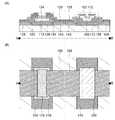
図1には、本実施の形態に係る半導体装置の構成の一例を示す。図1(A)は断面図であ
り、図1(B)は平面図である。図1(A)は、図1(B)のA−Bにおける断面を表す
ものである。なお、平面図においては、簡単のため、一部の構成を省略している。<Configuration example of semiconductor device>
FIG. 1 shows an example of the configuration of the semiconductor device according to this embodiment. 1A is a cross-sectional view, and FIG. 1B is a plan view. FIG. 1A illustrates a cross section taken along line AB of FIG. In the plan view, a part of the configuration is omitted for simplicity.
図1に示す半導体装置は、酸化物半導体を用いた第1のトランジスタ154および第2の
トランジスタ156に係るものであり、基板100(例えば、絶縁表面を有する基板)と
、基板100上の第1のゲート電極108および第2のゲート電極110と、第1のゲー
ト電極108および第2のゲート電極110を覆うゲート絶縁層112と、ゲート絶縁層
112上に設けられ、第1のゲート電極108と重畳する第1の酸化物半導体層118と
、ゲート絶縁層112上に設けられ、第2のゲート電極110と重畳する第2の酸化物半
導体層150と、第1の酸化物半導体層118と電気的に接続し、また、第1の導電層1
26と第2の導電層128の積層構造でなる第1のソース電極またはドレイン電極138
(および第1のソース電極またはドレイン電極140)と、第2の酸化物半導体層150
と電気的に接続し、第1の導電層126と第2の導電層128の積層構造でなる第2のソ
ース電極またはドレイン電極142(および第2のソース電極またはドレイン電極144
)と、を有する(図1(A)、図1(B)参照)。The semiconductor device illustrated in FIG. 1 is related to the
26 and the second
(And the first source or drain electrode 140) and the second
And the second source electrode or drain electrode 142 (and the second source electrode or
(See FIGS. 1A and 1B).
なお、第1の酸化物半導体層118には、第1の導電層126と第2の導電層128のう
ち、第1の導電層126のみが接触しており、かつ、第1のソース電極またはドレイン電
極138(第1のソース電極またはドレイン電極140)の一部は、第1の酸化物半導体
層118の上方に存在している。また、第2の酸化物半導体層150には、第1の導電層
126と第2の導電層128が接触し、かつ、第2の酸化物半導体層150の一部は、第
2のソース電極またはドレイン電極142(第2のソース電極またはドレイン電極144
)の上方に存在する。Note that, of the first
) Above.
第1の酸化物半導体層118上には、第1の導電層126と第2の導電層128のエッチ
ングの際のエッチングストッパーとして機能する保護層124が形成されている。また、
第1のトランジスタ154および第2のトランジスタ156を覆うように、絶縁層152
が形成されている。Over the first
The insulating
Is formed.
上記において、各トランジスタにおけるソース電極やドレイン電極は、キャリアの流れる
方向によってその機能が入れ替わるため、ソース電極およびドレイン電極の称呼は便宜的
なものに過ぎない。つまり、各電極の機能は、その称呼に限定して解釈されるものではな
い。また、各電極は、配線としての機能を有していても良い。In the above, the functions of the source electrode and the drain electrode in each transistor are switched depending on the direction in which carriers flow, and thus the names of the source electrode and the drain electrode are merely convenient. That is, the function of each electrode is not interpreted as being limited to the designation. Each electrode may have a function as a wiring.
ここで、第1のトランジスタはpチャネル型トランジスタであり、第2のトランジスタは
nチャネル型トランジスタであることが望ましい。この場合、第1の酸化物半導体層の一
部は、pチャネル型トランジスタのチャネル形成領域として機能し、第2の酸化物半導体
層の一部は、nチャネル型トランジスタのチャネル形成領域として機能することになる。
なお、第1の酸化物半導体層は、例えば、酸化錫、酸化亜鉛、酸化ニッケル、銅アルミ酸
化物、酸化ストロンチウム銅などを含む材料を用いて形成すると好適である。Here, the first transistor is preferably a p-channel transistor, and the second transistor is preferably an n-channel transistor. In this case, part of the first oxide semiconductor layer functions as a channel formation region of the p-channel transistor, and part of the second oxide semiconductor layer functions as a channel formation region of the n-channel transistor. It will be.
Note that the first oxide semiconductor layer is preferably formed using a material containing, for example, tin oxide, zinc oxide, nickel oxide, copper aluminum oxide, strontium copper oxide, or the like.
なお、トランジスタ154およびトランジスタ156においては、第1のソース電極また
はドレイン電極138(第1のソース電極またはドレイン電極140)と第2のソース電
極またはドレイン電極142(第2のソース電極またはドレイン電極144)を異なる材
料による積層構造としている。そして、第1の酸化物半導体層118と第1のソース電極
またはドレイン電極138(第1のソース電極またはドレイン電極140)との接続関係
を、第2の酸化物半導体層150と第2のソース電極またはドレイン電極142(第2の
ソース電極またはドレイン電極144)との接続関係とは異なるものにしている。より具
体的には、第2の酸化物半導体層150には、第1の導電層126と第2の導電層128
が接触するが、第1の酸化物半導体層118には、第1の導電層126と第2の導電層1
28のうち、第1の導電層126のみが接触する構成となっている。Note that in the
Are in contact with each other, but the first
28, only the first
これにより、電極に起因する特性劣化の問題がnチャネル型トランジスタと比較して深刻
なpチャネル型トランジスタの特性を十分に発揮させることが可能になる。なお、当該効
果を十分に発揮させるためには、第1の導電層126に用いられる第1の材料および第2
の導電層128に用いられる第2の材料として、仕事関数が所定の条件を満たすものを用
いることが望ましい。例えば、pチャネル型トランジスタである第1のトランジスタ15
4において、第1の酸化物半導体層118と接触する第1の導電層126に用いる材料(
第1の材料)は、第1の酸化物半導体層118の価電子帯との関係で決定することができ
る。具体的には、第1の酸化物半導体層118の価電子帯との間に形成されるショットキ
ー障壁が0.5eV以下となる材料を用いることが望ましい。また、例えば、nチャネル
型トランジスタである第2のトランジスタ156において、第2の酸化物半導体層150
と主として接触する第2の導電層128に用いる材料(第2の材料)は、第2の酸化物半
導体層150の伝導帯との関係で決定することができる。具体的には、第2の酸化物半導
体層150の伝導帯との間に形成されるショットキー障壁が0.5eV以下となる材料を
用いることが望ましい。より具体的には、例えば、第1の導電層126に用いられる第1
の材料を仕事関数が5.0eV(好ましくは5.2eV)より大きい材料とし、第2の導
電層128に用いられる第2の材料を仕事関数が4.8eV(好ましくは4.5eV)よ
り小さい材料とすると良い。As a result, it is possible to sufficiently exhibit the characteristics of the p-channel transistor in which the problem of characteristic deterioration due to the electrode is serious as compared with the n-channel transistor. Note that in order to sufficiently exhibit the effect, the first material and the second material used for the first
As the second material used for the
4, the material used for the first
The first material) can be determined in relation to the valence band of the first
A material (second material) used for the second
The material having a work function larger than 5.0 eV (preferably 5.2 eV) and the second material used for the second
このような材料を用いて第1の導電層126および第2の導電層128を形成することに
より、pチャネル型トランジスタにおける正孔の注入性を十分に確保することができる。
これにより、nチャネル型トランジスタとpチャネル型トランジスタとを同一基板上に形
成する場合(同一工程で形成する場合を含む)であっても、pチャネル型トランジスタの
特性劣化を防止することができる。つまり、半導体装置の特性を向上させることが可能で
ある。By forming the first
Accordingly, even when the n-channel transistor and the p-channel transistor are formed over the same substrate (including the case where they are formed in the same process), the characteristic deterioration of the p-channel transistor can be prevented. That is, the characteristics of the semiconductor device can be improved.
また、上述の如き構成を採用する場合には、トランジスタ毎に異なる電極を形成する必要
がないため、マスクの使用枚数増加を抑制し、半導体装置の製造コストを低減することが
できる。または、工程数を削減し、半導体装置の生産性を向上させることができる。Further, in the case of adopting the above-described configuration, it is not necessary to form different electrodes for each transistor, so that an increase in the number of masks used can be suppressed and the manufacturing cost of the semiconductor device can be reduced. Alternatively, the number of steps can be reduced and the productivity of the semiconductor device can be improved.
なお、上記のトランジスタを用いてCMOS回路を構成することもできる。この場合、第
1のゲート電極108と第2のゲート電極110とが電気的に接続され、第1のソース電
極またはドレイン電極138(または、第1のソース電極またはドレイン電極140)と
、第2のソース電極またはドレイン電極142(または、第2のソース電極またはドレイ
ン電極144)とが電気的に接続された構成を一部に用いれば良い。Note that a CMOS circuit can be formed using any of the above transistors. In this case, the
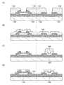
<半導体装置の作製方法例>
次に、上述の半導体装置の作製方法の一例について、図2乃至図4を用いて説明する。<Example of Manufacturing Method of Semiconductor Device>
Next, an example of a method for manufacturing the above semiconductor device will be described with reference to FIGS.
はじめに、基板100(例えば、絶縁表面を有する基板)上に導電層102を形成する(
図2(A)参照)。First, the
(See FIG. 2A).
基板100は、絶縁表面を有する基板であればよく、例えば、ガラス基板とすることがで
きる。ガラス基板は無アルカリガラス基板であることが好ましい。無アルカリガラス基板
には、例えば、アルミノシリケートガラス、アルミノホウケイ酸ガラス、バリウムホウケ
イ酸ガラス等のガラス材料が用いられる。他にも、基板100として、セラミック基板、
石英基板やサファイア基板等の絶縁体でなる絶縁体基板、シリコン等の半導体材料でなる
半導体基板の表面を絶縁材料で被覆したもの、金属やステンレス等の導電体でなる導電体
基板の表面を絶縁材料で被覆したものを用いることができる。また、作製工程の熱処理に
耐えられるのであれば、プラスチック基板などを用いることもできる。The
Insulating the surface of an insulator substrate made of an insulator such as a quartz substrate or a sapphire substrate, the surface of a semiconductor substrate made of a semiconductor material such as silicon covered with an insulating material, or the surface of a conductor substrate made of a conductor such as metal or stainless steel Those coated with a material can be used. Alternatively, a plastic substrate or the like can be used as long as it can withstand the heat treatment in the manufacturing process.
導電層102は、アルミニウム(Al)、銅(Cu)、モリブデン(Mo)、タングステ
ン(W)、チタン(Ti)等の導電性材料で形成することが望ましい。形成方法としては
、スパッタリング法や真空蒸着法などがある。なお、導電層102にアルミニウム(また
は銅)を用いる場合、アルミニウム単体(または銅単体)では耐熱性が低く、腐蝕しやす
い等の問題点があるため、耐熱性導電性材料と組み合わせて形成することが好ましい。The
耐熱性導電性材料としては、チタン(Ti)、タンタル(Ta)、タングステン(W)、
モリブデン(Mo)、クロム(Cr)、Nd(ネオジム)、スカンジウム(Sc)から選
ばれた元素を含む金属、上述した元素を成分とする合金、上述した元素を組み合わせた合
金、または上述した元素を成分とする窒化物などを用いることができる。これらの耐熱性
導電性材料とアルミニウム(または銅)を積層させて、導電層102を形成すればよい。Examples of heat-resistant conductive materials include titanium (Ti), tantalum (Ta), tungsten (W),
A metal containing an element selected from molybdenum (Mo), chromium (Cr), Nd (neodymium), and scandium (Sc), an alloy containing the above elements as a component, an alloy combining the above elements, or the above elements. A nitride or the like as a component can be used. The
図示しないが、基板100上には下地層を設けても良い。下地層は、基板100からの不
純物の拡散を防止する機能を有する。つまり、下地層を設けることより、半導体装置の信
頼性向上という課題を解決することができる。下地層は、窒化シリコン、酸化シリコンな
どの各種絶縁材料を用いて、単層構造または積層構造で形成すればよい。具体的には、例
えば、基板100側から窒化シリコンと酸化シリコンを順に積層した構成とするのが好適
である。なお、窒化シリコンは、不純物に対するブロッキング効果が極めて高いという特
徴を有している。Although not shown, a base layer may be provided on the
次に、導電層102上に選択的にレジストマスク104およびレジストマスク106を形
成し、これらを用いて導電層102を選択的にエッチングすることで、ゲート電極108
およびゲート電極110を形成する(図2(B)参照)。Next, a resist
Then, the
レジストマスク104およびレジストマスク106は、レジスト材料の塗布、フォトマス
クを用いた露光、現像等の工程を経ることにより形成される。レジスト材料の塗布には、
スピンコート法などの方法を適用することができる。なお、レジストマスク104および
レジストマスク106は、液滴吐出法やスクリーン印刷法などを用いて選択的に形成して
も良い。この場合、フォトマスクを用いる工程が不要になるため、生産性向上という課題
を解決することが可能である。なお、レジストマスク104およびレジストマスク106
は、導電層102のエッチングによりゲート電極108およびゲート電極110が形成さ
れた後には除去される。The resist
A method such as a spin coating method can be applied. Note that the resist
Is removed after the
上述のエッチングには、ドライエッチングを用いても良いし、ウエットエッチングを用い
ても良い。また、後に形成されるゲート絶縁層等の被覆性を向上し、段切れを防止するた
めに、ゲート電極108およびゲート電極110がテーパー形状となるようエッチングし
ても良い。この場合、例えば、テーパー角が20°以上90°未満となるような形状とす
ることが好ましい。ここで、「テーパー角」とは、テーパー形状を有する層の側面と底面
とがなす角をいう。As the above-described etching, dry etching or wet etching may be used. In addition, the
次に、ゲート電極108およびゲート電極110を覆うように、ゲート絶縁層112を形
成する(図2(C)参照)。ゲート絶縁層112は、酸化シリコン、酸化窒化シリコン、
窒化シリコン、窒化酸化シリコン、酸化アルミニウム、酸化タンタル等の材料を用いて形
成することができる。また、これらの材料からなる膜を積層させて形成しても良い。これ
らの膜は、スパッタ法をはじめとする各種の成膜法を用いて厚さが5nm以上250nm
以下となるように形成すると好ましい。例えば、ゲート絶縁層112として、スパッタ法
を用いて、酸化シリコン膜を100nmの厚さで形成することができる。もちろん、CV
D法などの他の方法を用いてゲート絶縁層112を形成しても良い。Next, the
It can be formed using a material such as silicon nitride, silicon nitride oxide, aluminum oxide, or tantalum oxide. Alternatively, films formed using these materials may be stacked. These films have a thickness of 5 nm to 250 nm by using various film forming methods including a sputtering method.
It is preferable to form the following. For example, a silicon oxide film with a thickness of 100 nm can be formed as the
The
また、スパッタ法とCVD法(プラズマCVD法など)とを組み合わせて、積層構造のゲ
ート絶縁層112を形成しても良い。例えば、ゲート絶縁層112の下層(ゲート電極1
08およびゲート電極110と接する部位)をプラズマCVD法により形成し、ゲート絶
縁層112の上層をスパッタ法により形成することができる。プラズマCVD法は、段差
被覆性の良い膜を形成することが容易であるため、ゲート電極108およびゲート電極1
10の直上の膜を形成する方法として適している。また、スパッタ法では、プラズマCV
D法と比較して、膜中の水素濃度を低減することが容易であるため、スパッタ法による膜
を半導体層と接する領域に設けることで、ゲート絶縁層112中の水素が半導体層中へ拡
散することを防止できる。特に、酸化物半導体材料を用いて半導体層を形成する場合には
、水素が特性に与える影響は極めて大きいため、このような構成を採用することは効果的
である。Alternatively, the
08 and a portion in contact with the gate electrode 110) can be formed by a plasma CVD method, and an upper layer of the
It is suitable as a method for forming a film immediately above 10. In the sputtering method, plasma CV
Compared with the D method, it is easy to reduce the hydrogen concentration in the film. Therefore, by providing a film by sputtering in a region in contact with the semiconductor layer, hydrogen in the
なお、本明細書等において、酸化窒化物とは、その組成において、窒素よりも酸素の含有
量(原子数)が多いものを示し、例えば、酸化窒化シリコンとは、酸素が50原子%以上
70原子%以下、窒素が0.5原子%以上15原子%以下、シリコンが25原子%以上3
5原子%以下、水素が0.1原子%以上10原子%以下の範囲で含まれるものをいう。ま
た、窒化酸化物とは、その組成において、酸素よりも窒素の含有量(原子数)が多いもの
を示し、例えば、窒化酸化シリコンとは、酸素が5原子%以上30原子%以下、窒素が2
0原子%以上55原子%以下、シリコンが25原子%以上35原子%以下、水素が10原
子%以上25原子%以下の範囲で含まれるものをいう。但し、上記範囲は、ラザフォード
後方散乱法(RBS:Rutherford Backscattering Spec
trometry)や、水素前方散乱法(HFS:Hydrogen Forward
Scattering)を用いて測定した場合のものである。また、構成元素の含有比率
の合計は100原子%を超えない。Note that in this specification and the like, the term “oxynitride” refers to a composition whose oxygen content (number of atoms) is higher than that of nitrogen. For example, silicon oxynitride refers to oxygen at 50 atomic% or more and 70 Atomic% or less, nitrogen is 0.5 atomic% or more and 15 atomic% or less, and silicon is 25 atomic% or more 3
5 atomic percent or less, and hydrogen is contained in the range of 0.1 atomic percent to 10 atomic percent. In addition, a nitrided oxide indicates a composition whose nitrogen content (number of atoms) is higher than that of oxygen. For example, silicon nitride oxide refers to an oxygen content of 5 atomic% to 30 atomic% and nitrogen content. 2
This includes silicon atoms in the range of 0 to 55 atom%, silicon in the range of 25 to 35 atom%, and hydrogen in the range of 10 to 25 atom%. However, the above range is Rutherford Backscattering Spec (RBS).
trometry and hydrogen forward scattering (HFS)
It is a thing at the time of measuring using Scattering. Further, the total content ratio of the constituent elements does not exceed 100 atomic%.
次に、ゲート絶縁層112を覆うように酸化物半導体層114を形成する(図2(D)参
照)。本実施の形態においては、酸化物半導体層114として、pチャネル型トランジス
タのチャネル形成領域として用いることができる酸化物半導体層を形成する。具体的には
、例えば、酸化錫、酸化亜鉛、酸化ニッケル、銅アルミ酸化物、酸化ストロンチウム銅の
いずれかを含むように酸化物半導体層114を形成する。作製方法の一例としては、上記
材料を含有するターゲットを用いたスパッタ法などがある。上記のスパッタ法としては、
スパッタ用電源に高周波電源を用いるRFスパッタ法や、直流電源を用いるDCスパッタ
法、パルス的に直流バイアスを加えるパルスDCスパッタ法などを用いることができる。
なお、pチャネル型トランジスタを実現できるのであれば、上記材料、方法を用いて酸化
物半導体層114を形成することに限定する必要はない。また、酸化物半導体層114の
膜厚は、5nm〜200nm程度とすればよい。Next, the
An RF sputtering method using a high frequency power source as a sputtering power source, a DC sputtering method using a DC power source, a pulse DC sputtering method in which a DC bias is applied in a pulsed manner, or the like can be used.
Note that as long as a p-channel transistor can be realized, the
本実施の形態においては、酸化物半導体層114を単層で形成する場合について示してい
るが、酸化物半導体層114は積層構造としても良い。例えば、後の第1のソース電極ま
たはドレイン電極138(第1のソース電極またはドレイン電極140)と第1の酸化物
半導体層118とが接触する領域のみに導電性を高めた酸化物半導体層を形成しても良い
。導電性を高めた酸化物半導体層は、構成元素の比率を異ならせることで実現することが
できる。このような構成を採用することにより、ソース電極またはドレイン電極と酸化物
半導体層との電気的な接続を良好なものにして、素子特性を向上させることができる。Although this embodiment shows the case where the
次に、酸化物半導体層114上に選択的にレジストマスク116を形成し、該レジストマ
スク116を用いて酸化物半導体層114を選択的にエッチングすることで、島状の第1
の酸化物半導体層118を形成する(図3(A)参照)。ここで、レジストマスク116
は、レジストマスク104およびレジストマスク106と同様の方法で形成することがで
きる。また、レジストマスク116は、酸化物半導体層114のエッチングにより第1の
酸化物半導体層118が形成された後には除去される。Next, a resist
The
Can be formed by a method similar to that for the resist
酸化物半導体層114のエッチングの方法としては、ウエットエッチングまたはドライエ
ッチングを用いることができる。ウエットエッチングに用いるエッチャント(エッチング
液)やドライエッチングに用いるエッチングガスは、酸化物半導体層114をエッチング
できるものであれば特に限定されない。例えば、ウエットエッチングを用いる場合には、
酢酸と硝酸と燐酸との混合液を用いることができる。また、ドライエッチングを行う場合
には、例えば、塩素を含有するガスや、塩素を含有するガスに酸素が添加されたガスを用
いると良い。As a method for etching the
A mixed solution of acetic acid, nitric acid and phosphoric acid can be used. When dry etching is performed, for example, a gas containing chlorine or a gas in which oxygen is added to a gas containing chlorine may be used.
なお、ドライエッチングには、反応性イオンエッチング法(RIE法)を用いたエッチン
グ装置や、ECR(Electron Cyclotron Resonance)やI
CP(Inductively Coupled Plasma)などの高密度プラズマ
源を用いたドライエッチング装置を用いることができる。また、ICPエッチング装置と
比べて広い面積に渡って一様な放電が得られるECCP(Enhanced Capac
itively Coupled Plasma)モードのエッチング装置を用いても良
い。ECCPモードのエッチング装置であれば、基板として第10世代以降の基板を用い
るような場合においても対応が容易である。For dry etching, an etching apparatus using a reactive ion etching method (RIE method), ECR (Electron Cyclotron Resonance), I
A dry etching apparatus using a high-density plasma source such as CP (Inductively Coupled Plasma) can be used. In addition, an ECCP (Enhanced Capac) can obtain a uniform discharge over a wide area as compared with an ICP etching apparatus.
It is also possible to use an etching device of an actively coupled plasma) mode. The ECCP mode etching apparatus can easily cope with a case where a 10th generation or later substrate is used as the substrate.
次に、第1の酸化物半導体層118を覆うように、絶縁層120を形成する(図3(B)
参照)。絶縁層120は、後のエッチングストップ層の元になる絶縁層であるから、後に
形成される導電層と選択比が取れる材料を用いて形成することが望ましい。絶縁層120
は、例えば、酸化シリコン、酸化窒化シリコン、窒化シリコン、窒化酸化シリコン、酸化
アルミニウム、酸化タンタル等の材料を用いて形成することができる。また、絶縁層12
0は、スパッタ法やCVD法をはじめとする各種の成膜法を用いて形成することができる
。なお、エッチングストップ層を設けない構成とする場合には、当該絶縁層120は形成
しなくとも良い。Next, the insulating
reference). Since the insulating
Can be formed using a material such as silicon oxide, silicon oxynitride, silicon nitride, silicon nitride oxide, aluminum oxide, or tantalum oxide. Insulating layer 12
0 can be formed using various film forming methods including a sputtering method and a CVD method. Note that in the case where the etching stop layer is not provided, the insulating
次に、絶縁層120上に選択的にレジストマスク122を形成し、該レジストマスク12
2を用いて絶縁層120を選択的にエッチングすることで、保護層124を形成する(図
3(C)参照)。ここで、レジストマスク122は、レジストマスク104等と同様の方
法で形成することができる。また、レジストマスク122は、絶縁層120のエッチング
により保護層124が形成された後には除去される。Next, a resist
The
次に、第1の酸化物半導体層118、保護層124およびゲート絶縁層112を覆うよう
に、第1の導電層126および第2の導電層128を形成する(図3(D)参照)。ここ
で、第1の導電層および第2の導電層は、異なる材料を用いて形成することが望ましい。
具体的には、pチャネル型トランジスタのソース電極またはドレイン電極として適当な材
料を用いて第1の導電層126を形成し、nチャネル型トランジスタのソース電極または
ドレイン電極として適当な材料を用いて第2の導電層128を形成する。これにより、形
成されるトランジスタの特性を十分に確保することが可能になる。Next, the first
Specifically, the first
例えば、第1の導電層126に用いられる第1の材料を仕事関数が5.0eV(好ましく
は5.2eV)より大きい材料とし、第2の導電層128に用いられる第2の材料を仕事
関数が4.8eV(好ましくは4.5eV)より小さい材料とすると良い。これは、第1
の材料として第1の酸化物半導体層の価電子帯との間に形成されるショットキー障壁が0
.5eV以下となる材料を用い、第2の材料として第2の酸化物半導体層の伝導帯との間
に形成されるショットキー障壁が0.5eV以下となる材料を用いる、と言い換えても良
い。このような材料を選択することにより、第1の酸化物半導体層118と第1の導電層
126との間のショットキー障壁によって第1の酸化物半導体層へのホールの注入性が低
下することを抑制できる。また、同様に、後のnチャネル型トランジスタを構成する第2
の酸化物半導体層150への電子の注入性が低下することを抑制できる。For example, the first material used for the first
The Schottky barrier formed between the valence band of the first oxide semiconductor layer as the material of the first oxide semiconductor layer is 0
. In other words, a material with 5 eV or less is used, and a material with a Schottky barrier formed between the conduction band of the second oxide semiconductor layer and 0.5 eV or less is used as the second material. By selecting such a material, the property of injecting holes into the first oxide semiconductor layer is reduced by the Schottky barrier between the first
It can be suppressed that the injectability of electrons into the
第1の導電層126に用いられる第1の材料としては、例えば、金、白金、ニッケル、銅
、コバルト、インジウム錫酸化物などがある。また、第2の導電層128に用いられる第
2の材料としては、チタン、アルミニウム、モリブデン、タングステンなどがある。これ
らの材料からなる第1の導電層126および第2の導電層128をスパッタリング法や真
空蒸着法などの成膜方法を用いて形成すればよい。Examples of the first material used for the first
なお、p型酸化物半導体材料の価電子帯のエネルギーの詳細は不明であるが、酸化錫にお
いては仕事関数が5.0eV(好ましくは5.2eV)より大きい電極材料を用いること
で良好なトランジスタ特性が得られることを確認しており、これは他のp型酸化物半導体
材料に関しても同様であるといえる。一方で、n型酸化物半導体材料の伝導帯のエネルギ
ーは、例えば、In−Ga−Zn系酸化物において約4.3eVであり、仕事関数が4.
8eV(好ましくは4.5eV)より小さい電極材料を用いる場合には、良好なトランジ
スタ特性が得られることを確認している。なお、n型酸化物半導体材料において、伝導帯
のエネルギーは3〜5eV程度であることが知られている。Note that details of the energy of the valence band of the p-type oxide semiconductor material are unknown, but in tin oxide, a good transistor can be obtained by using an electrode material having a work function larger than 5.0 eV (preferably 5.2 eV). It has been confirmed that characteristics can be obtained, and this can be said to be the same for other p-type oxide semiconductor materials. On the other hand, the energy of the conduction band of the n-type oxide semiconductor material is, for example, about 4.3 eV in an In—Ga—Zn-based oxide, and the work function is 4.
It has been confirmed that good transistor characteristics can be obtained when an electrode material smaller than 8 eV (preferably 4.5 eV) is used. Note that in an n-type oxide semiconductor material, it is known that the energy of the conduction band is about 3 to 5 eV.
次に、第2の導電層128上に選択的にレジストマスク130、レジストマスク132、
レジストマスク134およびレジストマスク136を形成し、該レジストマスクを用いて
第1の導電層126および第2の導電層128を選択的にエッチングすることで、第1の
酸化物半導体層に接続する第1のソース電極またはドレイン電極138、第1のソース電
極またはドレイン電極140、および、後にnチャネル型トランジスタの酸化物半導体層
と接続する第2のソース電極またはドレイン電極142、第2のソース電極またはドレイ
ン電極144を形成する(図4(A)参照)。上記レジストマスクは、レジストマスク1
04等と同様の方法で形成することができる。また、上記レジストマスクは、第1の導電
層126および第2の導電層128がエッチングされた後には除去される。Next, a resist
A resist
It can be formed by the same method as 04. The resist mask is removed after the first
次に、第1の導電層126と第2の導電層128の積層構造でなる第2のソース電極また
はドレイン電極142、および第2のソース電極またはドレイン電極144を覆うように
、酸化物半導体層146を形成する(図4(B)参照)。本実施の形態においては、酸化
物半導体層146として、nチャネル型トランジスタのチャネル形成領域として用いるこ
とができる酸化物半導体層を形成する。具体的には、例えば、InMO3(ZnO)m(
m>0)で表記されるものを用いて酸化物半導体層146を形成すると良い。ここで、M
は、ガリウム(Ga)、鉄(Fe)、ニッケル(Ni)、マンガン(Mn)、コバルト(
Co)などから選ばれた一の金属元素または複数の金属元素を示す。例えばMとしてGa
が選択される場合には、Gaのみの場合の他に、GaとNiや、GaとFeなど、Ga以
外の上記金属元素が選択される場合を含む。また、上記酸化物半導体において、Mとして
含まれる金属元素の他に、不純物元素としてFe、Niその他の遷移金属元素、または該
遷移金属の酸化物が含まれているものがある。もちろん、酸化物半導体材料は上記の材料
に限定されず、酸化亜鉛や酸化インジウムをはじめとする各種酸化物半導体材料を用いる
ことができる。作製方法は酸化物半導体層114の場合と同様であるから、詳細について
は酸化物半導体層114の作製方法を参酌すればよい。Next, the oxide semiconductor layer is formed so as to cover the second source or
The
Are gallium (Ga), iron (Fe), nickel (Ni), manganese (Mn), cobalt (
One metal element or a plurality of metal elements selected from Co) and the like. For example, Ga as M
In addition to the case of Ga alone, the case where the metal element other than Ga such as Ga and Ni or Ga and Fe is selected is included. In addition to the metal element contained as M, some of the above oxide semiconductors contain Fe, Ni, other transition metal elements, or oxides of the transition metal as impurity elements. Needless to say, the oxide semiconductor material is not limited to the above materials, and various oxide semiconductor materials including zinc oxide and indium oxide can be used. The manufacturing method is similar to that of the
なお、本実施の形態においては、酸化物半導体層146を単層で形成する場合について示
しているが、酸化物半導体層146は積層構造としても良い。例えば、第2のソース電極
またはドレイン電極142(第2のソース電極またはドレイン電極144)と第2の酸化
物半導体層150とが接触する領域のみに導電性を高めた酸化物半導体層を形成しても良
い。導電性を高めた酸化物半導体層は、構成元素の比率を異ならせることで実現すること
ができる。このような構成を採用することにより、ソース電極またはドレイン電極と酸化
物半導体層との電気的な接続を良好なものにして、素子特性を向上させることができる。Note that although the case where the
次に、酸化物半導体層146上に選択的にレジストマスク148を形成し、該レジストマ
スク148を用いて酸化物半導体層146を選択的にエッチングすることで、島状の第2
の酸化物半導体層150を形成する(図4(C)参照)。ここで、レジストマスク148
は、レジストマスク104等と同様の方法で形成することができる。また、レジストマス
ク148は、酸化物半導体層146のエッチングにより第2の酸化物半導体層150が形
成された後には除去される。なお、当該エッチングの詳細は、酸化物半導体層114のエ
ッチングの詳細を参酌すればよい。Next, a resist
The
Can be formed by a method similar to that for the resist
次に、第1のソース電極またはドレイン電極138、第1のソース電極またはドレイン電
極140、第2のソース電極またはドレイン電極142、第2のソース電極またはドレイ
ン電極144、第1の酸化物半導体層118、第2の酸化物半導体層150などを覆うよ
うに絶縁層152を形成する(図4(D)参照)。これにより、第1のトランジスタ15
4および第2のトランジスタ156を有する半導体装置が完成する。ここで、絶縁層15
2は、いわゆる層間絶縁層にあたる。絶縁層152は、酸化シリコン、酸化アルミニウム
、酸化タンタル等の材料を用いて形成することができる。また、これらの材料からなる膜
を積層させて形成しても良い。Next, the first source or
A semiconductor device having the fourth and
Reference numeral 2 denotes a so-called interlayer insulating layer. The insulating
本実施の形態において開示する構成において、ソース電極またはドレイン電極は、いずれ
も第1の導電層126と第2の導電層128との積層構造で形成されている。このため、
pチャネル型トランジスタとnチャネル型トランジスタでは異なる構造を有することにな
る。つまり、pチャネル型トランジスタにおいては、第1の酸化物半導体層118の上方
(または側面)に接するように、第1のソース電極またはドレイン電極138、および第
1のソース電極またはドレイン電極140が形成されるのに対して、nチャネル型トラン
ジスタにおいては、第2の酸化物半導体層150の下方(または側面)に接するように、
第2のソース電極またはドレイン電極142、および第2のソース電極またはドレイン電
極144が形成される。In the structure disclosed in this embodiment, each of the source electrode and the drain electrode is formed using a stacked structure of the first
The p-channel transistor and the n-channel transistor have different structures. That is, in the p-channel transistor, the first source or
A second source or
ここで、第1の導電層126に第2の材料を用い、第2の導電層128に第1の材料を用
いる場合には、pチャネル型トランジスタとnチャネル型トランジスタの構造を入れ替え
ることが可能である(この場合、第1の酸化物半導体層118に第2の材料を用いてnチ
ャネル型トランジスタを形成し、第2の酸化物半導体層150に第1の材料を用いてpチ
ャネル型トランジスタを形成することになる)。しかし、この場合には、第1の導電層1
26と第2の導電層128が共に接することになり、半導体装置の特性に与える影響の大
きいpチャネル型トランジスタの特性が悪化するおそれもあるため、可能な限り上述の構
成を採用することが望ましい。Here, in the case where the second material is used for the first
26 and the second
なお、第1の酸化物半導体層118や第2の酸化物半導体層150を形成した後には、1
00℃〜500℃、代表的には200℃〜400℃の熱処理を行うことが望ましい。当該
熱処理によって、半導体素子の特性を向上させるとともに、特性ばらつきを低減させるこ
とができる。熱処理の雰囲気は、例えば、大気雰囲気や窒素雰囲気、酸素雰囲気、水蒸気
雰囲気等とすることができる。また、熱処理時間は、0.1時間〜5時間程度とすればよ
い。熱処理のタイミングは、第1の酸化物半導体層118の元になる酸化物半導体層11
4の形成後や、第2の酸化物半導体層150の元になる酸化物半導体層146の形成後で
あれば特に限定されない。Note that after the first
It is desirable to perform heat treatment at 00 ° C. to 500 ° C., typically 200 ° C. to 400 ° C. By the heat treatment, characteristics of the semiconductor element can be improved and variation in characteristics can be reduced. The heat treatment atmosphere can be, for example, an air atmosphere, a nitrogen atmosphere, an oxygen atmosphere, a water vapor atmosphere, or the like. Further, the heat treatment time may be about 0.1 hour to 5 hours. The timing of the heat treatment is the
4 and after the formation of the
また、本実施の形態において用いたレジストマスクは、いずれも、多階調マスクを用いて
形成することができる。ここで、多階調マスクとは、多段階の光量で露光を行うことが可
能なマスクをいう。これを用いることで、一度の露光および現像工程によって、複数(代
表的には2種類)の厚さを有するレジストマスクを形成することができる。つまり、多階
調マスクを用いることで、工程数の増加を抑制することができる。In addition, any of the resist masks used in this embodiment can be formed using a multi-tone mask. Here, the multi-tone mask means a mask that can be exposed with multi-level light quantity. By using this, a resist mask having a plurality of (typically two types) thicknesses can be formed by a single exposure and development process. That is, an increase in the number of steps can be suppressed by using a multi-tone mask.
以上、本実施の形態において示した電極の材料および構造を採用することにより、nチャ
ネル型トランジスタおよびpチャネル型トランジスタの特性を十分に発揮させることがで
きる。これにより、半導体装置の特性を向上させることが可能である。または、このよう
な構成を採用することにより、マスクの使用枚数増加を抑制し、半導体装置の製造コスト
を低減することができる。または、工程数を削減し、半導体装置の生産性を向上させるこ
とができる。As described above, by employing the electrode material and structure described in this embodiment, the characteristics of the n-channel transistor and the p-channel transistor can be sufficiently exhibited. As a result, the characteristics of the semiconductor device can be improved. Alternatively, by employing such a configuration, an increase in the number of masks used can be suppressed, and the manufacturing cost of the semiconductor device can be reduced. Alternatively, the number of steps can be reduced and the productivity of the semiconductor device can be improved.
このように、開示する発明の一態様は、酸化物半導体を用いた好適な構造のnチャネル型
トランジスタおよびpチャネル型トランジスタを提供し、または、酸化物半導体を用いた
nチャネル型トランジスタおよびpチャネル型トランジスタの好適な作製方法を提供する
ことができるという点で極めて有用である。Thus, according to one embodiment of the disclosed invention, an n-channel transistor and a p-channel transistor having an appropriate structure using an oxide semiconductor are provided, or an n-channel transistor and a p-channel using an oxide semiconductor are provided. This is extremely useful in that a suitable method for manufacturing a type transistor can be provided.
(実施の形態2)
本実施の形態では、半導体装置の別の構成例について、図5を用いて説明し、半導体装置
の作製方法の別の例について、図6を用いて説明する。なお、本実施の形態において説明
する半導体装置の構成は、多くの点で、先の実施の形態において説明した半導体装置の構
成と共通している。このため、以下では、主として異なる部分について説明することとす
る。(Embodiment 2)
In this embodiment, another example of the structure of the semiconductor device will be described with reference to FIGS. 5A to 5C, and another example of a method for manufacturing the semiconductor device will be described with reference to FIGS. Note that the structure of the semiconductor device described in this embodiment is similar in many respects to the structure of the semiconductor device described in the above embodiment. For this reason, hereinafter, different parts will be mainly described.
<半導体装置の構成例>
図5には、本実施の形態に係る半導体装置の構成の一例を示す。図5(A)は断面図であ
り、図5(B)は平面図である。図5(A)は、図5(B)のA−Bにおける断面を表す
ものである。なお、平面図においては、簡単のため、一部の構成を省略している。<Configuration example of semiconductor device>
FIG. 5 shows an example of the configuration of the semiconductor device according to this embodiment. FIG. 5A is a cross-sectional view, and FIG. 5B is a plan view. FIG. 5A illustrates a cross section taken along line AB of FIG. In the plan view, a part of the configuration is omitted for simplicity.
図5に示す半導体装置は、酸化物半導体を用いた第1のトランジスタ228および第2の
トランジスタ230に係るものであり、基板100(例えば、絶縁表面を有する基板)と
、基板100上の第1のゲート電極108および第2のゲート電極110と、第1のゲー
ト電極108および第2のゲート電極110を覆うゲート絶縁層112と、ゲート絶縁層
112上に設けられ、第1のゲート電極108と重畳する第1の酸化物半導体層212と
、ゲート絶縁層112上に設けられ、第2のゲート電極110と重畳する第2の酸化物半
導体層222と、第1の酸化物半導体層212と電気的に接続し、また、第1の導電層1
26と第2の導電層128の積層構造でなる第1のソース電極またはドレイン電極214
(および第1のソース電極またはドレイン電極216)と、第2の酸化物半導体層222
と電気的に接続し、第1の導電層126と第2の導電層128の積層構造でなる第2のソ
ース電極またはドレイン電極218(および第2のソース電極またはドレイン電極220
)と、を有する(図5(A)、図5(B)参照)。The semiconductor device illustrated in FIG. 5 is related to the
26 and the second
(And the first source or drain electrode 216) and the second
And the second source or drain electrode 218 (and the second source or
(See FIGS. 5A and 5B).
ここで、上記半導体装置と、先の実施の形態において説明した半導体装置との相違の一は
、エッチングストッパーとして機能する保護層124の有無にある。すなわち、本実施の
形態において説明する半導体装置においては、保護層124が存在しない。また、これに
伴い、第1の酸化物半導体層118の一部がエッチング除去されることにより、第1の酸
化物半導体層212が形成されている。そして、第2の酸化物半導体層222、第1のソ
ース電極またはドレイン電極214(第1のソース電極またはドレイン電極216)、お
よび第2のソース電極またはドレイン電極218(第2のソース電極またはドレイン電極
220)の形成工程の関係から、第1のソース電極またはドレイン電極214(第1のソ
ース電極またはドレイン電極216)上には酸化物半導体層224および酸化物半導体層
226が存在し、第2の酸化物半導体層の形状も、先の実施の形態とは大きく異なるもの
になっている。Here, one of the differences between the semiconductor device and the semiconductor device described in the above embodiment is the presence or absence of the
本実施の形態に示すように、エッチングストッパーとして機能する保護層124を形成し
ない場合には、半導体装置の製造コストを一層低減することができる。または、工程数を
削減し、半導体装置の生産性を向上させることができる。As shown in this embodiment mode, in the case where the
<半導体装置の作製方法例>
次に、上述の半導体装置の作製方法の一例について、図6を用いて説明する。なお、第1
の酸化物半導体層118の形成までは、先の実施の形態と同様であるため、詳細について
は先の実施の形態を参酌すればよい(図2(A)〜図2(D)、および図3(A)参照)
。<Example of Manufacturing Method of Semiconductor Device>
Next, an example of a method for manufacturing the above semiconductor device will be described with reference to FIGS. The first
The formation of the
.
第1の酸化物半導体層118を形成した後には、第1の酸化物半導体層118およびゲー
ト絶縁層112を覆うように、第1の導電層126および第2の導電層128を形成する
(図6(A)参照)。第1の導電層126および第2の導電層128の詳細については先
の実施の形態を参酌することができる。After the first
次に、第2の導電層128上に選択的にレジストマスク200、レジストマスク202お
よびレジストマスク204を形成し、該レジストマスクを用いて第1の導電層126およ
び第2の導電層128を選択的にエッチングする(図6(B)参照)。これにより、ゲー
ト電極110と重畳する領域のゲート絶縁層112の一部が露出する。レジストマスクお
よびエッチングの詳細については先の実施の形態を参酌すればよい。Next, a resist
次に、第1の導電層126と第2の導電層128の積層構造およびゲート絶縁層112を
覆うように、酸化物半導体層146を形成する(図6(C)参照)。酸化物半導体層14
6の詳細についても、先の実施の形態を参酌できる。Next, the
For the details of 6, the previous embodiment can be referred to.
次に、酸化物半導体層146上に選択的にレジストマスク206、レジストマスク208
およびレジストマスク210を形成し、該レジストマスクを用いて、第1の導電層126
、第2の導電層128および酸化物半導体層146を選択的にエッチングすることで、第
1の酸化物半導体層118の一部がエッチングされた第1の酸化物半導体層212、これ
に接続する第1のソース電極またはドレイン電極214および第1のソース電極またはド
レイン電極216、第2のソース電極またはドレイン電極218および第2のソース電極
またはドレイン電極220、これに接続する第2の酸化物半導体層222を形成する(図
6(D)参照)。レジストマスクおよびエッチングの詳細については先の実施の形態を参
酌できる。Next, a resist
And a resist
The second
なお、第1のソース電極またはドレイン電極214および第1のソース電極またはドレイ
ン電極216の上方には、酸化物半導体層146のエッチングによって酸化物半導体層2
24および酸化物半導体層226が残存することになるが、これによってトランジスタ特
性に大きな変動が生じることはない。Note that the oxide semiconductor layer 2 is etched by etching the
24 and the
その後、第1のソース電極またはドレイン電極214、第1のソース電極またはドレイン
電極216、第2のソース電極またはドレイン電極218、第2のソース電極またはドレ
イン電極220、第1の酸化物半導体層212、第2の酸化物半導体層222などを覆う
ように絶縁層152を形成する(図6(E)参照)。これにより、第1のトランジスタ2
28および第2のトランジスタ230を有する半導体装置が完成する。ここで、絶縁層1
52は、いわゆる層間絶縁層にあたる。詳細については先の実施の形態を参酌すればよい
。After that, the first source or
A semiconductor device having 28 and the
52 is a so-called interlayer insulating layer. For details, the previous embodiment may be referred to.
以上、本実施の形態において示した電極の材料および構造を採用することにより、nチャ
ネル型トランジスタおよびpチャネル型トランジスタの特性を十分に発揮させることがで
きる。これにより、半導体装置の特性を向上させることが可能である。または、このよう
な構成を採用することにより、マスクの使用枚数増加を抑制し、半導体装置の製造コスト
を低減することができる。または、工程数を削減し、半導体装置の生産性を向上させるこ
とができる。As described above, by employing the electrode material and structure described in this embodiment, the characteristics of the n-channel transistor and the p-channel transistor can be sufficiently exhibited. As a result, the characteristics of the semiconductor device can be improved. Alternatively, by employing such a configuration, an increase in the number of masks used can be suppressed, and the manufacturing cost of the semiconductor device can be reduced. Alternatively, the number of steps can be reduced and the productivity of the semiconductor device can be improved.
さらに、本実施の形態においてはエッチングストッパーとして機能する保護層を形成しな
いため、半導体装置の製造コストを一層低減することができる。または、工程数を削減し
、半導体装置の生産性を向上させることができる。Further, since the protective layer functioning as an etching stopper is not formed in this embodiment mode, the manufacturing cost of the semiconductor device can be further reduced. Alternatively, the number of steps can be reduced and the productivity of the semiconductor device can be improved.
なお、本実施の形態は、先の実施の形態と適宜組み合わせて用いることができる。Note that this embodiment can be combined with any of the above embodiments as appropriate.
(実施の形態3)
本実施の形態では、半導体装置の別の構成例について、図7を用いて説明し、半導体装置
の作製方法の別の例について、図8および図9を用いて説明する。なお、本実施の形態に
おいて説明する半導体装置の構成は、多くの点で、先の実施の形態において説明した半導
体装置の構成と共通している。このため、以下では、主として異なる部分について説明す
ることとする。(Embodiment 3)
In this embodiment, another example of a structure of a semiconductor device will be described with reference to FIGS. 7A to 7C, and another example of a method for manufacturing a semiconductor device will be described with reference to FIGS. Note that the structure of the semiconductor device described in this embodiment is similar in many respects to the structure of the semiconductor device described in the above embodiment. For this reason, hereinafter, different parts will be mainly described.
<半導体装置の構成例>
図7には、本実施の形態に係る半導体装置の構成の一例を示す。図7(A)は断面図であ
り、図7(B)は平面図である。図7(A)は、図7(B)のA−Bにおける断面を表す
ものである。なお、平面図においては、簡単のため、一部の構成を省略している。<Configuration example of semiconductor device>
FIG. 7 shows an example of the configuration of the semiconductor device according to this embodiment. FIG. 7A is a cross-sectional view, and FIG. 7B is a plan view. FIG. 7A illustrates a cross section taken along line AB of FIG. In the plan view, a part of the configuration is omitted for simplicity.
図7に示す半導体装置は、酸化物半導体を用いた第1のトランジスタ322および第2の
トランジスタ324に係るものであり、基板100(例えば、絶縁表面を有する基板)と
、基板100上の第1のゲート電極108および第2のゲート電極110と、第1のゲー
ト電極108および第2のゲート電極110を覆うゲート絶縁層112と、ゲート絶縁層
112上に設けられ、第1のゲート電極108と重畳する第1の酸化物半導体層118と
、ゲート絶縁層112上に設けられ、第2のゲート電極110と重畳する第2の酸化物半
導体層150と、第1の酸化物半導体層118と電気的に接続し、また、第1の導電層1
26と第2の導電層128の積層構造でなる第1のソース電極またはドレイン電極312
(第1のソース電極またはドレイン電極314)と、第2の酸化物半導体層150と電気
的に接続し、第2の導電層128でなる第2のソース電極またはドレイン電極316(第
2のソース電極またはドレイン電極318)と、を有する(図7(A)、図7(B)参照
)。The semiconductor device illustrated in FIG. 7 is related to the
A first source electrode or a
The second source electrode or drain electrode 316 (second source) which is electrically connected to the
ここで、上記半導体装置と、先の実施の形態において説明した半導体装置との相違の一は
、第2のソース電極またはドレイン電極の構造にある。すなわち、本実施の形態において
説明する半導体装置においては、第2のソース電極またはドレイン電極が第2の導電層1
28のみで形成されている。このため、第2の酸化物半導体層150に第1の導電層12
6が接することはない。Here, one of the differences between the semiconductor device and the semiconductor device described in the above embodiment is a structure of a second source electrode or a drain electrode. That is, in the semiconductor device described in this embodiment, the second source electrode or the drain electrode is the second conductive layer 1.
28 only. Therefore, the first conductive layer 12 is formed on the second
6 never touches.
本実施の形態に示すように、第2のソース電極またはドレイン電極を第2の導電層128
のみで形成することにより、nチャネル型トランジスタの電極に適した材料(第2の材料
)を用いた導電層のみを第2の酸化物半導体層150に接触させることができるようにな
る。これにより、第1の導電層126が第2の酸化物半導体層150に接触する場合と比
較して、トランジスタ特性の向上が可能である。As shown in this embodiment mode, the second source electrode or the drain electrode is used as the second
Thus, only the conductive layer using the material (second material) suitable for the electrode of the n-channel transistor can be brought into contact with the second
<半導体装置の作製方法例>
次に、上述の半導体装置の作製方法の一例について、図8および図9を用いて説明する。
なお、保護層124の形成までは、先の実施の形態と同様であるため、詳細については先
の実施の形態を参酌すればよい(図2(A)〜図2(D)、および図3(A)〜図3(C
)参照)。<Example of Manufacturing Method of Semiconductor Device>
Next, an example of a method for manufacturing the above semiconductor device will be described with reference to FIGS.
Note that the process up to the formation of the
)reference).
保護層124を形成した後には、保護層124、第1の酸化物半導体層118およびゲー
ト絶縁層112を覆うように、第1の導電層126を形成する(図8(A)参照)。第1
の導電層126の詳細については、先の実施の形態を参酌することができる。After the
The above embodiment can be referred to for details of the
次に、第1の導電層126上に選択的にレジストマスク300を形成し、該レジストマス
ク300を用いて第1の導電層126を選択的にエッチングして、第1の導電層302を
形成する(図8(B)参照)。これにより、ゲート電極110と重畳する領域、およびそ
の周辺の領域における第1の導電層126が除去される。レジストマスクおよびエッチン
グの詳細については先の実施の形態を参酌すればよい。Next, a resist
次に、第1の導電層302およびゲート絶縁層112を覆うように、第2の導電層128
を形成する(図8(C)参照)。これにより、ゲート電極110と重畳する領域、および
その周辺の領域において、ゲート絶縁層112上には第2の導電層128が形成されるこ
とになる。第2の導電層128の詳細についても、先の実施の形態を参酌することができ
る。Next, the second
(See FIG. 8C). Thus, the second
次に、第2の導電層128上に選択的にレジストマスク304、レジストマスク306、
レジストマスク308およびレジストマスク310を形成し、該レジストマスクを用いて
第1の導電層302および第2の導電層128を選択的にエッチングして、第1のソース
電極またはドレイン電極312および第1のソース電極またはドレイン電極314、第2
のソース電極またはドレイン電極316および第2のソース電極またはドレイン電極31
8を形成する(図8(D)参照)。レジストマスクおよびエッチングの詳細については、
先の実施の形態を参酌すればよい。Next, a resist
A resist
Source electrode or
8 is formed (see FIG. 8D). For more information on resist masks and etching,
The previous embodiment may be taken into consideration.
次に、第2の導電層128でなる第2のソース電極またはドレイン電極316、および第
2のソース電極またはドレイン電極318を覆うように、酸化物半導体層146を形成す
る(図9(A)参照)。酸化物半導体層146の詳細については、先の実施の形態を参酌
できる。Next, the
次に、酸化物半導体層146上に選択的にレジストマスク320を形成し、該レジストマ
スクを用いて、酸化物半導体層146を選択的にエッチングすることで、第2の酸化物半
導体層150を形成する(図9(B)参照)。レジストマスクおよびエッチングの詳細に
ついては先の実施の形態を参酌できる。Next, a resist
その後、第1のソース電極またはドレイン電極312、第1のソース電極またはドレイン
電極314、第2のソース電極またはドレイン電極316、第2のソース電極またはドレ
イン電極318、第1の酸化物半導体層118、第2の酸化物半導体層150などを覆う
ように絶縁層152を形成する(図9(C)参照)。これにより、第1のトランジスタ3
22および第2のトランジスタ324を有する半導体装置が完成する。ここで、絶縁層1
52は、いわゆる層間絶縁層にあたる。詳細については先の実施の形態を参酌すればよい
。After that, the first source or
A semiconductor device having 22 and the
52 is a so-called interlayer insulating layer. For details, the previous embodiment may be referred to.
以上、本実施の形態において示した電極の材料および構造を採用することにより、nチャ
ネル型トランジスタおよびpチャネル型トランジスタの特性を十分に発揮させることがで
きる。これにより、半導体装置の特性を向上させることが可能である。または、このよう
な構成を採用することにより、マスクの使用枚数増加を抑制し、半導体装置の製造コスト
を低減することができる。または、工程数を削減し、半導体装置の生産性を向上させるこ
とができる。As described above, by employing the electrode material and structure described in this embodiment, the characteristics of the n-channel transistor and the p-channel transistor can be sufficiently exhibited. As a result, the characteristics of the semiconductor device can be improved. Alternatively, by employing such a configuration, an increase in the number of masks used can be suppressed, and the manufacturing cost of the semiconductor device can be reduced. Alternatively, the number of steps can be reduced and the productivity of the semiconductor device can be improved.
さらに、第2のソース電極またはドレイン電極を第2の導電層のみで形成することにより
、nチャネル型トランジスタの電極に適した材料(第2の材料)を用いた導電層のみを第
2の酸化物半導体層に接触させることができる。これにより、第1の導電層が第2の酸化
物半導体層に接触する場合と比較して、トランジスタ特性を向上させることができる。Further, by forming the second source electrode or the drain electrode only with the second conductive layer, only the conductive layer using the material (second material) suitable for the electrode of the n-channel transistor is subjected to the second oxidation. The physical semiconductor layer can be contacted. Accordingly, the transistor characteristics can be improved as compared with the case where the first conductive layer is in contact with the second oxide semiconductor layer.
なお、本実施の形態は、先の実施の形態と適宜組み合わせて用いることができる。Note that this embodiment can be combined with any of the above embodiments as appropriate.
(実施の形態4)
先の実施の形態において説明したトランジスタを用いてCMOS回路を構成した場合の回
路特性について、計算機シミュレーションを用いて確認を行った。本実施の形態では、そ
の結果について説明する。(Embodiment 4)
The circuit characteristics in the case where a CMOS circuit is configured using the transistors described in the previous embodiment were confirmed using computer simulation. In this embodiment, the result will be described.
計算機シミュレーションは、シルバコ社製デバイスシミュレータATLASを用いて行っ
た。なお、本実施の形態においては、CMOS回路の特性を調査するために、CMOS回
路を用いたリングオシレータに関して計算機シミュレーションを行った。なお、リングオ
シレータはCMOSインバータ回路を奇数段直列に接続させることにより構成される。つ
まり、リングオシレータを構成するnチャネル型トランジスタの数とpチャネル型トラン
ジスタの数は等しい。また、リングオシレータの発振周波数は、デバイス性能の目安とす
ることができる。The computer simulation was performed using a device simulator ATLAS manufactured by Silvaco. In this embodiment, in order to investigate the characteristics of the CMOS circuit, a computer simulation was performed on a ring oscillator using the CMOS circuit. The ring oscillator is configured by connecting CMOS inverter circuits in odd-numbered stages in series. That is, the number of n-channel transistors and the number of p-channel transistors constituting the ring oscillator are equal. Further, the oscillation frequency of the ring oscillator can be used as a measure of device performance.
図10に酸化物半導体を用いたnチャネル型トランジスタのゲート電圧(Vg)−ドレイ
ン電流(Id)曲線を示す。また、図11に酸化物半導体を用いたpチャネル型トランジ
スタのゲート電圧(Vg)−ドレイン電流(Id)曲線を示す。共に、横軸はゲート電圧
(Vg)を表し、縦軸はドレイン電流(Id)を表す。また、実線はドレイン電圧が0.
25(V)の場合、破線はドレイン電圧が10(V)の場合の曲線である。ここで、nチ
ャネル型トランジスタのチャネル長(L)を10μm、チャネル幅(W)を10μmとし
、pチャネル型トランジスタのチャネル長(L)を10μm、チャネル幅(W)を20μ
mとした。また、ゲート絶縁層の膜厚を100nm、誘電率を4.1、半導体層の膜厚を
50nmとした。FIG. 10 shows a gate voltage (Vg) -drain current (Id) curve of an n-channel transistor using an oxide semiconductor. FIG. 11 shows a gate voltage (Vg) -drain current (Id) curve of a p-channel transistor using an oxide semiconductor. In both cases, the horizontal axis represents the gate voltage (Vg), and the vertical axis represents the drain current (Id). The solid line shows a drain voltage of 0.
In the case of 25 (V), the broken line is a curve when the drain voltage is 10 (V). Here, the channel length (L) of the n-channel transistor is 10 μm, the channel width (W) is 10 μm, the channel length (L) of the p-channel transistor is 10 μm, and the channel width (W) is 20 μm.
m. The thickness of the gate insulating layer was 100 nm, the dielectric constant was 4.1, and the thickness of the semiconductor layer was 50 nm.
nチャネル型トランジスタの半導体層については、バンドギャップを3.05eV、電子
親和力を4.3eV、仕事関数を4.3eV、電子移動度を15cm2/V・s、ホール
移動度を0.1 cm2/V・sとし、pチャネル型トランジスタの半導体層については
、バンドギャップを3.0eV、電子親和力を2.8eV、仕事関数を5.5eV、電子
移動度を0.1cm2/V・s、ホール移動度を1.0cm2/V・sとして計算を行っ
た。また、オフ電流を計算する際は、バンド間トンネルによるリーク電流を仮定した。な
お、上記pチャネル型トランジスタにおいて、オンオフ比は約2桁であった。For the semiconductor layer of the n-channel transistor, the band gap is 3.05 eV, the electron affinity is 4.3 eV, the work function is 4.3 eV, the electron mobility is 15 cm2 / V · s, and the hole mobility is 0.1 cm.2 / V · s, and the semiconductor layer of the p-channel transistor has a band gap of 3.0 eV, an electron affinity of 2.8 eV, a work function of 5.5 eV, and an electron mobility of 0.1 cm2 / V · s. The calculation was performed with the hole mobility being 1.0 cm2 / V · s. Further, when calculating the off-current, a leak current due to a band-to-band tunnel was assumed. In the p-channel transistor, the on / off ratio was about two digits.
上述のnチャネル型トランジスタおよびpチャネル型トランジスタを用いたCMOSイン
バータ回路を3段直列に接続した構成のリングオシレータにつき、発振の様子を確認した
。図12にその結果を示す。横軸は時間(s)を表し、縦軸は電圧(V)を表す。ここで
、電源電圧は15(V)としている。図12から、一周期が約5nsであり、発振周波数
は約200MHzであることが分かる。The state of oscillation was confirmed for a ring oscillator having a configuration in which three stages of CMOS inverter circuits using the above-described n-channel transistor and p-channel transistor were connected in series. FIG. 12 shows the result. The horizontal axis represents time (s), and the vertical axis represents voltage (V). Here, the power supply voltage is set to 15 (V). From FIG. 12, it can be seen that one period is about 5 ns and the oscillation frequency is about 200 MHz.
以上の通り、開示する発明の一態様である酸化物半導体トランジスタを用いて構成された
CMOS回路の動作が確認された。本実施の形態において用いたpチャネル型トランジス
タのオンオフ比は約2桁であり、十分な特性とはいいがたいものであるが、CMOS回路
としての動作に大きな問題はない。pチャネル型酸化物半導体材料の改良・発展によって
、CMOS回路のさらなる特性向上が可能である。As described above, the operation of the CMOS circuit including the oxide semiconductor transistor which is one embodiment of the disclosed invention was confirmed. The on / off ratio of the p-channel transistor used in this embodiment is about two digits, and although it is difficult to say that the characteristics are sufficient, there is no significant problem in the operation as a CMOS circuit. By improving and developing the p-channel oxide semiconductor material, the characteristics of the CMOS circuit can be further improved.
なお、このようなCMOS回路の実現には、開示する発明の一態様であるトランジスタの
構成は極めて有効である。Note that the transistor structure which is one embodiment of the disclosed invention is extremely effective for realizing such a CMOS circuit.
100 基板
102 導電層
104 レジストマスク
106 レジストマスク
108 ゲート電極
110 ゲート電極
112 ゲート絶縁層
114 酸化物半導体層
116 レジストマスク
118 酸化物半導体層
120 絶縁層
122 レジストマスク
124 保護層
126 導電層
128 導電層
130 レジストマスク
132 レジストマスク
134 レジストマスク
136 レジストマスク
138 第1のソース電極またはドレイン電極
140 第1のソース電極またはドレイン電極
142 第2のソース電極またはドレイン電極
144 第2のソース電極またはドレイン電極
146 酸化物半導体層
148 レジストマスク
150 酸化物半導体層
152 絶縁層
154 トランジスタ
156 トランジスタ
200 レジストマスク
202 レジストマスク
204 レジストマスク
206 レジストマスク
208 レジストマスク
210 レジストマスク
212 酸化物半導体層
214 第1のソース電極またはドレイン電極
216 第1のソース電極またはドレイン電極
218 第2のソース電極またはドレイン電極
220 第2のソース電極またはドレイン電極
222 酸化物半導体層
224 酸化物半導体層
226 酸化物半導体層
228 トランジスタ
230 トランジスタ
300 レジストマスク
302 導電層
304 レジストマスク
306 レジストマスク
308 レジストマスク
310 レジストマスク
312 第1のソース電極またはドレイン電極
314 第1のソース電極またはドレイン電極
316 第2のソース電極またはドレイン電極
318 第2のソース電極またはドレイン電極
320 レジストマスク
322 トランジスタ
324 トランジスタ100
Claims (4)
Translated fromJapanese前記第1の導電層上方の絶縁層と、
前記絶縁層上方の酸化物半導体層と、
前記酸化物半導体層上方の第2の導電層と、
前記酸化物半導体層上方の第3の導電層と、
前記第2の導電層上方の第4の導電層と、
前記第3の導電層上方の第5の導電層と、を有する半導体装置の作製方法であって、
第6の導電層をエッチングする工程を経て、前記第6の導電層から第7の導電層を形成し、
前記第7の導電層上方に第8の導電層を形成し、
前記第7の導電層及び前記第8の導電層をエッチングする工程を経て、前記第7の導電層から前記第2の導電層及び前記第3の導電層を形成し、且つ前記第8の導電層から前記第4の導電層及び前記第5の導電層を形成することを特徴とする半導体装置の作製方法。A first conductive layer;
An insulating layer above the first conductive layer;
An oxide semiconductor layer above the insulating layer;
A second conductive layer above the oxide semiconductor layer;
A third conductive layer above the oxide semiconductor layer;
A fourth conductive layer above the second conductive layer;
And a fifth conductive layer above the third conductive layer.
Through a step of etching the sixth conductive layer, a seventh conductive layer is formed from the sixth conductive layer,
Forming an eighth conductive layer above the seventh conductive layer;
Through the step of etching the seventh conductive layer and the eighth conductive layer, the second conductive layer and the third conductive layer are formed from the seventh conductive layer, and the eighth conductive layer is formed. A method for manufacturing a semiconductor device, wherein the fourth conductive layer and the fifth conductive layer are formed from a layer.
前記絶縁層は、前記第4の導電層又は前記第5の導電層と接する領域を有することを特徴とする半導体装置の作製方法。In claim 1,
The method for manufacturing a semiconductor device, wherein the insulating layer includes a region in contact with the fourth conductive layer or the fifth conductive layer.
前記絶縁層と接するように前記第8の導電層を形成することを特徴とする半導体装置の作製方法。In claim 1 or claim 2,
A method for manufacturing a semiconductor device, wherein the eighth conductive layer is formed in contact with the insulating layer.
前記第4の導電層は、前記第2の導電層と接する領域を有し、
前記第5の導電層は、前記第3の導電層と接する領域を有することを特徴とする半導体装置の作製方法。In any one of Claims 1 thru | or 3,
The fourth conductive layer has a region in contact with the second conductive layer,
The method for manufacturing a semiconductor device, wherein the fifth conductive layer includes a region in contact with the third conductive layer.
Priority Applications (1)
| Application Number | Priority Date | Filing Date | Title |
|---|---|---|---|
| JP2015237079AJP2016029749A (en) | 2009-04-10 | 2015-12-04 | Semiconductor device |
Applications Claiming Priority (3)
| Application Number | Priority Date | Filing Date | Title |
|---|---|---|---|
| JP2009095739 | 2009-04-10 | ||
| JP2009095739 | 2009-04-10 | ||
| JP2015237079AJP2016029749A (en) | 2009-04-10 | 2015-12-04 | Semiconductor device |
Related Parent Applications (1)
| Application Number | Title | Priority Date | Filing Date |
|---|---|---|---|
| JP2014182906ADivisionJP5852718B2 (en) | 2009-04-10 | 2014-09-09 | Semiconductor device |
Related Child Applications (1)
| Application Number | Title | Priority Date | Filing Date |
|---|---|---|---|
| JP2017153757ADivisionJP6346362B2 (en) | 2009-04-10 | 2017-08-09 | Semiconductor device and manufacturing method of semiconductor device |
Publications (1)
| Publication Number | Publication Date |
|---|---|
| JP2016029749Atrue JP2016029749A (en) | 2016-03-03 |
Family
ID=42933654
Family Applications (4)
| Application Number | Title | Priority Date | Filing Date |
|---|---|---|---|
| JP2010086822AActiveJP5615018B2 (en) | 2009-04-10 | 2010-04-05 | Semiconductor device and manufacturing method of semiconductor device |
| JP2014182906AActiveJP5852718B2 (en) | 2009-04-10 | 2014-09-09 | Semiconductor device |
| JP2015237079AWithdrawnJP2016029749A (en) | 2009-04-10 | 2015-12-04 | Semiconductor device |
| JP2017153757AExpired - Fee RelatedJP6346362B2 (en) | 2009-04-10 | 2017-08-09 | Semiconductor device and manufacturing method of semiconductor device |
Family Applications Before (2)
| Application Number | Title | Priority Date | Filing Date |
|---|---|---|---|
| JP2010086822AActiveJP5615018B2 (en) | 2009-04-10 | 2010-04-05 | Semiconductor device and manufacturing method of semiconductor device |
| JP2014182906AActiveJP5852718B2 (en) | 2009-04-10 | 2014-09-09 | Semiconductor device |
Family Applications After (1)
| Application Number | Title | Priority Date | Filing Date |
|---|---|---|---|
| JP2017153757AExpired - Fee RelatedJP6346362B2 (en) | 2009-04-10 | 2017-08-09 | Semiconductor device and manufacturing method of semiconductor device |
Country Status (5)
| Country | Link |
|---|---|
| US (1) | US8441047B2 (en) |
| JP (4) | JP5615018B2 (en) |
| KR (1) | KR101688399B1 (en) |
| CN (1) | CN101859710B (en) |
| TW (1) | TWI509800B (en) |
Families Citing this family (27)
| Publication number | Priority date | Publication date | Assignee | Title |
|---|---|---|---|---|
| KR102462043B1 (en)* | 2009-10-16 | 2022-11-03 | 가부시키가이샤 한도오따이 에네루기 켄큐쇼 | Semiconductor device |
| KR20120103676A (en) | 2009-12-04 | 2012-09-19 | 가부시키가이샤 한도오따이 에네루기 켄큐쇼 | Semiconductor device |
| KR101863941B1 (en)* | 2010-06-08 | 2018-06-04 | 삼성디스플레이 주식회사 | Thin film transistor with offset structure |
| JP5908263B2 (en)* | 2010-12-03 | 2016-04-26 | 株式会社半導体エネルギー研究所 | DC-DC converter |
| JP2012256020A (en)* | 2010-12-15 | 2012-12-27 | Semiconductor Energy Lab Co Ltd | Semiconductor device and driving method for the same |
| US9443984B2 (en) | 2010-12-28 | 2016-09-13 | Semiconductor Energy Laboratory Co., Ltd. | Semiconductor device and manufacturing method thereof |
| TWI570809B (en)* | 2011-01-12 | 2017-02-11 | 半導體能源研究所股份有限公司 | Semiconductor device and method of manufacturing same |
| US9799773B2 (en) | 2011-02-02 | 2017-10-24 | Semiconductor Energy Laboratory Co., Ltd. | Transistor and semiconductor device |
| TWI451573B (en) | 2011-03-17 | 2014-09-01 | E Ink Holdings Inc | Display device and thin film transistor structure thereof |
| US9634029B2 (en) | 2011-03-17 | 2017-04-25 | E Ink Holdings Inc. | Thin film transistor substrate and display device having same |
| TWI534956B (en)* | 2011-05-27 | 2016-05-21 | 半導體能源研究所股份有限公司 | Method for adjusting circuit and driving adjustment circuit |
| US9099885B2 (en)* | 2011-06-17 | 2015-08-04 | Semiconductor Energy Laboratory Co., Ltd. | Wireless power feeding system |
| US9082861B2 (en)* | 2011-11-11 | 2015-07-14 | Semiconductor Energy Laboratory Co., Ltd. | Transistor with oxide semiconductor channel having protective layer |
| US20160315196A1 (en)* | 2012-04-13 | 2016-10-27 | The Governors Of The University Of Alberta | Buried source schottky barrier thin film transistor and method of manufacture |
| JP6013084B2 (en)* | 2012-08-24 | 2016-10-25 | ルネサスエレクトロニクス株式会社 | Semiconductor device and manufacturing method of semiconductor device |
| JPWO2015025499A1 (en)* | 2013-08-19 | 2017-03-02 | 出光興産株式会社 | Oxide semiconductor substrate and Schottky barrier diode |
| CA2932446A1 (en)* | 2013-12-04 | 2015-06-11 | The Governors Of The University Of Alberta | Buried source schottky barrier thin film transistor and method of manufacture |
| JP6072858B2 (en)* | 2015-06-22 | 2017-02-01 | ルネサスエレクトロニクス株式会社 | Manufacturing method of semiconductor device |
| WO2018004009A1 (en)* | 2016-06-30 | 2018-01-04 | 株式会社Flosfia | p-TYPE OXIDE SEMICONDUCTOR AND METHOD FOR MANUFACTURING SAME |
| CN108172625B (en)* | 2016-12-07 | 2020-09-29 | 清华大学 | Logic circuit |
| KR102676341B1 (en) | 2016-12-30 | 2024-06-17 | 엘지디스플레이 주식회사 | Thin film transistor and method for manufacturing the same, and display device including the same |
| WO2018221294A1 (en)* | 2017-05-31 | 2018-12-06 | シャープ株式会社 | Active matrix substrate and method of manufacturing same |
| WO2019166791A1 (en)* | 2018-02-27 | 2019-09-06 | The University Of Manchester | Schottky barrier thin film transistor and method |
| JP6997990B2 (en)* | 2018-04-27 | 2022-01-18 | 株式会社タムラ製作所 | P-channel field effect transistor and semiconductor device for amplifier circuit |
| KR102469187B1 (en)* | 2018-09-04 | 2022-11-21 | 삼성디스플레이 주식회사 | Display device and method for manufacturing the same |
| US12040333B2 (en) | 2020-08-27 | 2024-07-16 | Semiconductor Energy Laboratory Co., Ltd. | Semiconductor device, display device, and electronic device |
| KR20220079442A (en)* | 2020-12-04 | 2022-06-13 | 가부시키가이샤 한도오따이 에네루기 켄큐쇼 | Display device and manufacturing method of display device |
Citations (2)
| Publication number | Priority date | Publication date | Assignee | Title |
|---|---|---|---|---|
| JP2007286150A (en)* | 2006-04-13 | 2007-11-01 | Idemitsu Kosan Co Ltd | Electro-optical device, current control TFT substrate, and manufacturing method thereof |
| JP2008134593A (en)* | 2006-11-28 | 2008-06-12 | Lg Phillips Lcd Co Ltd | Array substrate for liquid crystal display device and manufacturing method thereof |
Family Cites Families (102)
| Publication number | Priority date | Publication date | Assignee | Title |
|---|---|---|---|---|
| JPS60198861A (en) | 1984-03-23 | 1985-10-08 | Fujitsu Ltd | Thin film transistor |
| JP3479375B2 (en) | 1995-03-27 | 2003-12-15 | 科学技術振興事業団 | Metal oxide semiconductor device in which a pn junction is formed with a thin film transistor made of a metal oxide semiconductor such as cuprous oxide, and methods for manufacturing the same |
| KR100394896B1 (en) | 1995-08-03 | 2003-11-28 | 코닌클리케 필립스 일렉트로닉스 엔.브이. | A semiconductor device including a transparent switching element |
| JP3625598B2 (en) | 1995-12-30 | 2005-03-02 | 三星電子株式会社 | Manufacturing method of liquid crystal display device |
| US5612228A (en)* | 1996-04-24 | 1997-03-18 | Motorola | Method of making CMOS with organic and inorganic semiconducting region |
| JP3597468B2 (en)* | 1998-06-19 | 2004-12-08 | シン フイルム エレクトロニクス エイエスエイ | Integrated inorganic / organic complementary type thin film transistor circuit and method of manufacturing the same |
| JP4170454B2 (en) | 1998-07-24 | 2008-10-22 | Hoya株式会社 | Article having transparent conductive oxide thin film and method for producing the same |
| JP2000150861A (en) | 1998-11-16 | 2000-05-30 | Tdk Corp | Oxide thin film |
| JP3276930B2 (en) | 1998-11-17 | 2002-04-22 | 科学技術振興事業団 | Transistor and semiconductor device |
| TW460731B (en) | 1999-09-03 | 2001-10-21 | Ind Tech Res Inst | Electrode structure and production method of wide viewing angle LCD |
| JP4089858B2 (en) | 2000-09-01 | 2008-05-28 | 国立大学法人東北大学 | Semiconductor device |
| KR20020038482A (en) | 2000-11-15 | 2002-05-23 | 모리시타 요이찌 | Thin film transistor array, method for producing the same, and display panel using the same |
| JP3997731B2 (en) | 2001-03-19 | 2007-10-24 | 富士ゼロックス株式会社 | Method for forming a crystalline semiconductor thin film on a substrate |
| JP2002289859A (en) | 2001-03-23 | 2002-10-04 | Minolta Co Ltd | Thin film transistor |
| JP3925839B2 (en) | 2001-09-10 | 2007-06-06 | シャープ株式会社 | Semiconductor memory device and test method thereof |
| JP4090716B2 (en) | 2001-09-10 | 2008-05-28 | 雅司 川崎 | Thin film transistor and matrix display device |
| WO2003040441A1 (en) | 2001-11-05 | 2003-05-15 | Japan Science And Technology Agency | Natural superlattice homologous single crystal thin film, method for preparation thereof, and device using said single crystal thin film |
| JP4164562B2 (en) | 2002-09-11 | 2008-10-15 | 独立行政法人科学技術振興機構 | Transparent thin film field effect transistor using homologous thin film as active layer |
| JP4083486B2 (en) | 2002-02-21 | 2008-04-30 | 独立行政法人科学技術振興機構 | Method for producing LnCuO (S, Se, Te) single crystal thin film |
| CN1445821A (en) | 2002-03-15 | 2003-10-01 | 三洋电机株式会社 | Forming method of ZnO film and ZnO semiconductor layer, semiconductor element and manufacturing method thereof |
| JP3933591B2 (en) | 2002-03-26 | 2007-06-20 | 淳二 城戸 | Organic electroluminescent device |
| US7339187B2 (en) | 2002-05-21 | 2008-03-04 | State Of Oregon Acting By And Through The Oregon State Board Of Higher Education On Behalf Of Oregon State University | Transistor structures |
| JP2004022625A (en) | 2002-06-13 | 2004-01-22 | Murata Mfg Co Ltd | Semiconductor device and method of manufacturing the semiconductor device |
| US7105868B2 (en) | 2002-06-24 | 2006-09-12 | Cermet, Inc. | High-electron mobility transistor with zinc oxide |
| US7067843B2 (en) | 2002-10-11 | 2006-06-27 | E. I. Du Pont De Nemours And Company | Transparent oxide semiconductor thin film transistors |
| JP4166105B2 (en) | 2003-03-06 | 2008-10-15 | シャープ株式会社 | Semiconductor device and manufacturing method thereof |
| JP2004273732A (en) | 2003-03-07 | 2004-09-30 | Sharp Corp | Active matrix substrate and manufacturing method thereof |
| JP4108633B2 (en) | 2003-06-20 | 2008-06-25 | シャープ株式会社 | THIN FILM TRANSISTOR, MANUFACTURING METHOD THEREOF, AND ELECTRONIC DEVICE |
| US7262463B2 (en) | 2003-07-25 | 2007-08-28 | Hewlett-Packard Development Company, L.P. | Transistor including a deposited channel region having a doped portion |
| CN1998087B (en) | 2004-03-12 | 2014-12-31 | 独立行政法人科学技术振兴机构 | Amorphous oxide and thin film transistor |
| US7282782B2 (en) | 2004-03-12 | 2007-10-16 | Hewlett-Packard Development Company, L.P. | Combined binary oxide semiconductor device |
| US7297977B2 (en) | 2004-03-12 | 2007-11-20 | Hewlett-Packard Development Company, L.P. | Semiconductor device |
| US7145174B2 (en) | 2004-03-12 | 2006-12-05 | Hewlett-Packard Development Company, Lp. | Semiconductor device |
| US7211825B2 (en) | 2004-06-14 | 2007-05-01 | Yi-Chi Shih | Indium oxide-based thin film transistors and circuits |
| JP2006100760A (en) | 2004-09-02 | 2006-04-13 | Casio Comput Co Ltd | Thin film transistor and manufacturing method thereof |
| US7285501B2 (en) | 2004-09-17 | 2007-10-23 | Hewlett-Packard Development Company, L.P. | Method of forming a solution processed device |
| US7298084B2 (en) | 2004-11-02 | 2007-11-20 | 3M Innovative Properties Company | Methods and displays utilizing integrated zinc oxide row and column drivers in conjunction with organic light emitting diodes |
| US7453065B2 (en) | 2004-11-10 | 2008-11-18 | Canon Kabushiki Kaisha | Sensor and image pickup device |
| EP2453481B1 (en) | 2004-11-10 | 2017-01-11 | Canon Kabushiki Kaisha | Field effect transistor with amorphous oxide |
| AU2005302964B2 (en) | 2004-11-10 | 2010-11-04 | Canon Kabushiki Kaisha | Field effect transistor employing an amorphous oxide |
| US7829444B2 (en) | 2004-11-10 | 2010-11-09 | Canon Kabushiki Kaisha | Field effect transistor manufacturing method |
| US7863611B2 (en) | 2004-11-10 | 2011-01-04 | Canon Kabushiki Kaisha | Integrated circuits utilizing amorphous oxides |
| KR100953596B1 (en) | 2004-11-10 | 2010-04-21 | 캐논 가부시끼가이샤 | Light emitting device |
| US7791072B2 (en) | 2004-11-10 | 2010-09-07 | Canon Kabushiki Kaisha | Display |
| US7579224B2 (en) | 2005-01-21 | 2009-08-25 | Semiconductor Energy Laboratory Co., Ltd. | Method for manufacturing a thin film semiconductor device |
| TWI445178B (en) | 2005-01-28 | 2014-07-11 | Semiconductor Energy Lab | Semiconductor device, electronic device, and method of manufacturing semiconductor device |
| TWI505473B (en) | 2005-01-28 | 2015-10-21 | Semiconductor Energy Lab | Semiconductor device, electronic device, and method of manufacturing semiconductor device |
| US7858451B2 (en) | 2005-02-03 | 2010-12-28 | Semiconductor Energy Laboratory Co., Ltd. | Electronic device, semiconductor device and manufacturing method thereof |
| US7948171B2 (en) | 2005-02-18 | 2011-05-24 | Semiconductor Energy Laboratory Co., Ltd. | Light emitting device |
| US20060197092A1 (en) | 2005-03-03 | 2006-09-07 | Randy Hoffman | System and method for forming conductive material on a substrate |
| US8681077B2 (en) | 2005-03-18 | 2014-03-25 | Semiconductor Energy Laboratory Co., Ltd. | Semiconductor device, and display device, driving method and electronic apparatus thereof |
| US7544967B2 (en) | 2005-03-28 | 2009-06-09 | Massachusetts Institute Of Technology | Low voltage flexible organic/transparent transistor for selective gas sensing, photodetecting and CMOS device applications |
| US7645478B2 (en) | 2005-03-31 | 2010-01-12 | 3M Innovative Properties Company | Methods of making displays |
| US8300031B2 (en) | 2005-04-20 | 2012-10-30 | Semiconductor Energy Laboratory Co., Ltd. | Semiconductor device comprising transistor having gate and drain connected through a current-voltage conversion element |
| JP2006344849A (en) | 2005-06-10 | 2006-12-21 | Casio Comput Co Ltd | Thin film transistor |
| US7402506B2 (en) | 2005-06-16 | 2008-07-22 | Eastman Kodak Company | Methods of making thin film transistors comprising zinc-oxide-based semiconductor materials and transistors made thereby |
| US7691666B2 (en) | 2005-06-16 | 2010-04-06 | Eastman Kodak Company | Methods of making thin film transistors comprising zinc-oxide-based semiconductor materials and transistors made thereby |
| US7507618B2 (en) | 2005-06-27 | 2009-03-24 | 3M Innovative Properties Company | Method for making electronic devices using metal oxide nanoparticles |
| KR100711890B1 (en) | 2005-07-28 | 2007-04-25 | 삼성에스디아이 주식회사 | OLED display and manufacturing method thereof |
| JP2007059128A (en) | 2005-08-23 | 2007-03-08 | Canon Inc | Organic EL display device and manufacturing method thereof |
| JP5116225B2 (en) | 2005-09-06 | 2013-01-09 | キヤノン株式会社 | Manufacturing method of oxide semiconductor device |
| JP4850457B2 (en) | 2005-09-06 | 2012-01-11 | キヤノン株式会社 | Thin film transistor and thin film diode |
| JP2007073705A (en) | 2005-09-06 | 2007-03-22 | Canon Inc | Oxide semiconductor channel thin film transistor and method for manufacturing the same |
| JP4280736B2 (en) | 2005-09-06 | 2009-06-17 | キヤノン株式会社 | Semiconductor element |
| JP5078246B2 (en)* | 2005-09-29 | 2012-11-21 | 株式会社半導体エネルギー研究所 | Semiconductor device and manufacturing method of semiconductor device |
| EP1770788A3 (en) | 2005-09-29 | 2011-09-21 | Semiconductor Energy Laboratory Co., Ltd. | Semiconductor device having oxide semiconductor layer and manufacturing method thereof |
| JP5037808B2 (en) | 2005-10-20 | 2012-10-03 | キヤノン株式会社 | Field effect transistor using amorphous oxide, and display device using the transistor |
| CN101577231B (en) | 2005-11-15 | 2013-01-02 | 株式会社半导体能源研究所 | Semiconductor device and method of manufacturing the same |
| TWI292281B (en) | 2005-12-29 | 2008-01-01 | Ind Tech Res Inst | Pixel structure of active organic light emitting diode and method of fabricating the same |
| US7867636B2 (en) | 2006-01-11 | 2011-01-11 | Murata Manufacturing Co., Ltd. | Transparent conductive film and method for manufacturing the same |
| JP4977478B2 (en) | 2006-01-21 | 2012-07-18 | 三星電子株式会社 | ZnO film and method of manufacturing TFT using the same |
| US7576394B2 (en) | 2006-02-02 | 2009-08-18 | Kochi Industrial Promotion Center | Thin film transistor including low resistance conductive thin films and manufacturing method thereof |
| US7977169B2 (en) | 2006-02-15 | 2011-07-12 | Kochi Industrial Promotion Center | Semiconductor device including active layer made of zinc oxide with controlled orientations and manufacturing method thereof |
| KR20070101595A (en) | 2006-04-11 | 2007-10-17 | 삼성전자주식회사 | ZnO TFT |
| CN101060139A (en)* | 2006-04-17 | 2007-10-24 | 三星电子株式会社 | Amorphous zinc oxide thin film transistor and method of manufacturing the same |
| US20070252928A1 (en) | 2006-04-28 | 2007-11-01 | Toppan Printing Co., Ltd. | Structure, transmission type liquid crystal display, reflection type display and manufacturing method thereof |
| JP5028033B2 (en) | 2006-06-13 | 2012-09-19 | キヤノン株式会社 | Oxide semiconductor film dry etching method |
| JP4999400B2 (en) | 2006-08-09 | 2012-08-15 | キヤノン株式会社 | Oxide semiconductor film dry etching method |
| JP4609797B2 (en) | 2006-08-09 | 2011-01-12 | Nec液晶テクノロジー株式会社 | Thin film device and manufacturing method thereof |
| JP2008060201A (en)* | 2006-08-30 | 2008-03-13 | Seiko Epson Corp | Semiconductor device manufacturing method, thin film transistor and manufacturing method thereof, electro-optical device and manufacturing method thereof, and electronic apparatus |
| JP4332545B2 (en) | 2006-09-15 | 2009-09-16 | キヤノン株式会社 | Field effect transistor and manufacturing method thereof |
| JP4274219B2 (en) | 2006-09-27 | 2009-06-03 | セイコーエプソン株式会社 | Electronic devices, organic electroluminescence devices, organic thin film semiconductor devices |
| JP5164357B2 (en)* | 2006-09-27 | 2013-03-21 | キヤノン株式会社 | Semiconductor device and manufacturing method of semiconductor device |
| US7622371B2 (en) | 2006-10-10 | 2009-11-24 | Hewlett-Packard Development Company, L.P. | Fused nanocrystal thin film semiconductor and method |
| US7772021B2 (en) | 2006-11-29 | 2010-08-10 | Samsung Electronics Co., Ltd. | Flat panel displays comprising a thin-film transistor having a semiconductive oxide in its channel and methods of fabricating the same for use in flat panel displays |
| JP2008140684A (en) | 2006-12-04 | 2008-06-19 | Toppan Printing Co Ltd | Color EL display and manufacturing method thereof |
| KR101303578B1 (en) | 2007-01-05 | 2013-09-09 | 삼성전자주식회사 | Etching method of thin film |
| US8207063B2 (en) | 2007-01-26 | 2012-06-26 | Eastman Kodak Company | Process for atomic layer deposition |
| KR20080073944A (en)* | 2007-02-07 | 2008-08-12 | 엘지전자 주식회사 | Hybrid organic EL device and method for manufacturing same |
| JP4910779B2 (en)* | 2007-03-02 | 2012-04-04 | 凸版印刷株式会社 | Organic EL display and manufacturing method thereof |
| KR100851215B1 (en) | 2007-03-14 | 2008-08-07 | 삼성에스디아이 주식회사 | Thin film transistor and organic light emitting display device using same |
| US7795613B2 (en) | 2007-04-17 | 2010-09-14 | Toppan Printing Co., Ltd. | Structure with transistor |
| KR101325053B1 (en) | 2007-04-18 | 2013-11-05 | 삼성디스플레이 주식회사 | Thin film transistor substrate and manufacturing method thereof |
| KR20080094300A (en)* | 2007-04-19 | 2008-10-23 | 삼성전자주식회사 | Thin film transistors and methods of manufacturing the same and flat panel displays comprising thin film transistors |
| KR101334181B1 (en) | 2007-04-20 | 2013-11-28 | 삼성전자주식회사 | Thin Film Transistor having selectively crystallized channel layer and method of manufacturing the same |
| CN101663762B (en) | 2007-04-25 | 2011-09-21 | 佳能株式会社 | Oxynitride semiconductor |
| KR101345376B1 (en) | 2007-05-29 | 2013-12-24 | 삼성전자주식회사 | Fabrication method of ZnO family Thin film transistor |
| US8202365B2 (en) | 2007-12-17 | 2012-06-19 | Fujifilm Corporation | Process for producing oriented inorganic crystalline film, and semiconductor device using the oriented inorganic crystalline film |
| JP4623179B2 (en) | 2008-09-18 | 2011-02-02 | ソニー株式会社 | Thin film transistor and manufacturing method thereof |
| JP5451280B2 (en) | 2008-10-09 | 2014-03-26 | キヤノン株式会社 | Wurtzite crystal growth substrate, manufacturing method thereof, and semiconductor device |
| US8384439B2 (en)* | 2008-11-28 | 2013-02-26 | Samsung Electronics Co., Ltd. | Semiconductor devices and methods of fabricating the same |
| CN101840936B (en)* | 2009-02-13 | 2014-10-08 | 株式会社半导体能源研究所 | Semiconductor device including a transistor, and manufacturing method of the semiconductor device |
- 2010
- 2010-04-05JPJP2010086822Apatent/JP5615018B2/enactiveActive
- 2010-04-05USUS12/754,393patent/US8441047B2/enactiveActive
- 2010-04-07TWTW099110739Apatent/TWI509800B/enactive
- 2010-04-07CNCN201010161138.1Apatent/CN101859710B/ennot_activeExpired - Fee Related
- 2010-04-09KRKR1020100032575Apatent/KR101688399B1/enactiveActive
- 2014
- 2014-09-09JPJP2014182906Apatent/JP5852718B2/enactiveActive
- 2015
- 2015-12-04JPJP2015237079Apatent/JP2016029749A/ennot_activeWithdrawn
- 2017
- 2017-08-09JPJP2017153757Apatent/JP6346362B2/ennot_activeExpired - Fee Related
Patent Citations (2)
| Publication number | Priority date | Publication date | Assignee | Title |
|---|---|---|---|---|
| JP2007286150A (en)* | 2006-04-13 | 2007-11-01 | Idemitsu Kosan Co Ltd | Electro-optical device, current control TFT substrate, and manufacturing method thereof |
| JP2008134593A (en)* | 2006-11-28 | 2008-06-12 | Lg Phillips Lcd Co Ltd | Array substrate for liquid crystal display device and manufacturing method thereof |
Also Published As
| Publication number | Publication date |
|---|---|
| KR20100113039A (en) | 2010-10-20 |
| JP2015008327A (en) | 2015-01-15 |
| JP2010263195A (en) | 2010-11-18 |
| US20100258802A1 (en) | 2010-10-14 |
| KR101688399B1 (en) | 2016-12-21 |
| CN101859710A (en) | 2010-10-13 |
| TW201110346A (en) | 2011-03-16 |
| US8441047B2 (en) | 2013-05-14 |
| JP2017199941A (en) | 2017-11-02 |
| CN101859710B (en) | 2015-04-08 |
| JP5852718B2 (en) | 2016-02-03 |
| TWI509800B (en) | 2015-11-21 |
| JP6346362B2 (en) | 2018-06-20 |
| JP5615018B2 (en) | 2014-10-29 |
Similar Documents
| Publication | Publication Date | Title |
|---|---|---|
| JP6346362B2 (en) | Semiconductor device and manufacturing method of semiconductor device | |
| JP7713079B2 (en) | display device | |
| JP7543518B2 (en) | Display device | |
| US10475819B2 (en) | Semiconductor device | |
| JP5841622B2 (en) | Semiconductor device | |
| JP6659255B2 (en) | Thin film transistor | |
| Lee et al. | A three-mask-processed coplanar a-IGZO TFT with source and drain offsets | |
| JP2015005672A (en) | Oxide transistor | |
| Xu et al. | Back-Channel-etched IGZO TFTs with cu-based multilayer electrodes using MoAl alloy and MoMn alloy as buffer layers | |
| JP2025157351A (en) | display device |
Legal Events
| Date | Code | Title | Description |
|---|---|---|---|
| A621 | Written request for application examination | Free format text:JAPANESE INTERMEDIATE CODE: A621 Effective date:20151204 | |
| A977 | Report on retrieval | Free format text:JAPANESE INTERMEDIATE CODE: A971007 Effective date:20161025 | |
| A131 | Notification of reasons for refusal | Free format text:JAPANESE INTERMEDIATE CODE: A131 Effective date:20161115 | |
| A521 | Request for written amendment filed | Free format text:JAPANESE INTERMEDIATE CODE: A523 Effective date:20161206 | |
| A02 | Decision of refusal | Free format text:JAPANESE INTERMEDIATE CODE: A02 Effective date:20170523 | |
| A761 | Written withdrawal of application | Free format text:JAPANESE INTERMEDIATE CODE: A761 Effective date:20170809 |