JP2016025502A - Antenna for wireless power reception, and wearable device - Google Patents
Antenna for wireless power reception, and wearable deviceDownload PDFInfo
- Publication number
- JP2016025502A JP2016025502AJP2014148681AJP2014148681AJP2016025502AJP 2016025502 AJP2016025502 AJP 2016025502AJP 2014148681 AJP2014148681 AJP 2014148681AJP 2014148681 AJP2014148681 AJP 2014148681AJP 2016025502 AJP2016025502 AJP 2016025502A
- Authority
- JP
- Japan
- Prior art keywords
- circuit
- coiled circuit
- coiled
- coil
- wireless power
- Prior art date
- Legal status (The legal status is an assumption and is not a legal conclusion. Google has not performed a legal analysis and makes no representation as to the accuracy of the status listed.)
- Pending
Links
Images


Landscapes
- Coils Of Transformers For General Uses (AREA)
- Coils Or Transformers For Communication (AREA)
- Details Of Aerials (AREA)
Abstract
Description
Translated fromJapanese本発明は、ワイヤレス受電用アンテナ及びウエアラブルデバイスに関する。 The present invention relates to a wireless power receiving antenna and a wearable device.
近年、近距離無線通信(NFC:Near Field Communication)技術を利用したRFID(Radio Frequency IDentification)システムや非接触ICカード等の普及に伴い、平面的に形成したコイル状回路をアンテナとして使用する装置が広く利用されている。このような装置として、例えば電磁誘導現象を利用したワイヤレス(非接触式)の給電装置が知られている。このワイヤレス給電装置は、給電用アンテナ(一次側コイル)と対向する位置に受電用アンテナ(二次側コイル)を配置し、給電用アンテナに電流を流すことで生じる磁束により受電用アンテナに電流を発生させるものである。このようなアンテナは、携帯機器の充電装置として普及しつつある。 In recent years, with the spread of RFID (Radio Frequency IDentification) systems using near field communication (NFC) technology, non-contact IC cards, and the like, devices that use a planar coiled circuit as an antenna have been developed. Widely used. As such a device, for example, a wireless (non-contact type) power feeding device using an electromagnetic induction phenomenon is known. In this wireless power feeder, a power receiving antenna (secondary coil) is disposed at a position facing the power feeding antenna (primary coil), and a current is supplied to the power receiving antenna by a magnetic flux generated by passing a current through the power feeding antenna. Is generated. Such an antenna is becoming popular as a charging device for portable devices.
この携帯機器向けのアンテナには、小型で効率的な電力伝送が実現できることが求められる。このようなアンテナとして、例えばフレキシブルプリント配線板に形成した複数のコイル状回路を並列接続と直列接続とを組み合わせて接続するアンテナが提案されている(特開2013−241455号公報参照)。 This portable antenna is required to be able to realize small and efficient power transmission. As such an antenna, for example, an antenna has been proposed in which a plurality of coiled circuits formed on a flexible printed wiring board are connected in combination with parallel connection and series connection (see JP2013-241455A).
上述のようなアンテナは、ワイヤレス給電装置の給電用アンテナと受電用アンテナとが重なり合った状態に基づいて設計されているため、例えば給電用アンテナと受電用アンテナとの位置ずれにより給電用アンテナから供給する磁束の半分程度が受電用アンテナのコイルを通過しないような場合、電力の受信効率が著しく低下することがある。 Since the antenna as described above is designed based on the state where the power feeding antenna and the power receiving antenna of the wireless power feeding apparatus overlap each other, for example, the power feeding antenna and the power receiving antenna are supplied from the power feeding antenna due to a positional shift. When about half of the generated magnetic flux does not pass through the coil of the power receiving antenna, the power receiving efficiency may be significantly reduced.
本発明は、上述のような事情に基づいてなされたものであり、給電用アンテナと受電用アンテナとの位置ずれが生じても電力の受信効率の低下が少なく、小型化が可能なワイヤレス受電用アンテナの提供を目的とする。 The present invention has been made on the basis of the above-described circumstances, and for wireless power reception capable of miniaturization with little reduction in power reception efficiency even if a positional deviation between a power feeding antenna and a power receiving antenna occurs. The purpose is to provide an antenna.
上記課題を解決するためになされた本発明の一態様に係るワイヤレス受電用アンテナは、フレキシブルプリント配線板から構成され、このフレキシブルプリント配線板が、合成樹脂製の絶縁層と、この絶縁層の一方側面に積層され、第1コイル状回路を有する第1コイル層と、上記絶縁層の他方側面に積層され、第2コイル状回路を有する第2コイル層とを備えており、上記第1コイル状回路と上記第2コイル状回路とが平面視で重複領域を有する。 The antenna for wireless power reception according to one aspect of the present invention made to solve the above-described problem is composed of a flexible printed wiring board, and the flexible printed wiring board includes a synthetic resin insulating layer and one of the insulating layers. A first coil layer having a first coil-like circuit laminated on a side surface; and a second coil layer having a second coil-like circuit laminated on the other side surface of the insulating layer. The circuit and the second coiled circuit have an overlapping region in plan view.
本発明のワイヤレス受電用アンテナは、小型化が可能であると共に、給電用アンテナと受電用アンテナとの位置ずれが生じても電力の受信効率の低下を抑制できる。 The wireless power receiving antenna of the present invention can be miniaturized and can suppress a decrease in power reception efficiency even if a positional deviation occurs between the power feeding antenna and the power receiving antenna.
[本発明の実施形態の説明]
本発明の一態様に係るワイヤレス受電用アンテナは、フレキシブルプリント配線板から構成され、このフレキシブルプリント配線板が、合成樹脂製の絶縁層と、この絶縁層の一方側面に積層され、第1コイル状回路を有する第1コイル層と、上記絶縁層の他方側面に積層され、第2コイル状回路を有する第2コイル層とを備えており、上記第1コイル状回路と上記第2コイル状回路とが平面視で重複領域を有する。[Description of Embodiment of the Present Invention]
A wireless power receiving antenna according to an aspect of the present invention includes a flexible printed wiring board, and the flexible printed wiring board is laminated on a synthetic resin insulating layer and one side surface of the insulating layer to form a first coil shape. A first coil layer having a circuit; and a second coil layer having a second coiled circuit laminated on the other side surface of the insulating layer, the first coiled circuit, the second coiled circuit, Have overlapping regions in plan view.
当該ワイヤレス受電用アンテナは、第1コイル状回路と第2コイル状回路とが平面視で重複領域を有することで、この重複領域によりコイルの巻数の増加と同様の効果が得られるため、受電に必要な磁束を受けるアンテナの有効面積を増やすことができる。このため、当該ワイヤレス受電用アンテナは、給電用アンテナと受電用アンテナとの位置ずれによる電力の受信効率の低下が少なく、小型化が可能である。さらに、当該ワイヤレス受電用アンテナは、合成樹脂製の絶縁層の一方側の面に第1コイル状回路が積層され、他方側の面に第2コイル状回路が積層されるので、インダクタンスの調整においてコイルの面積や厚みの増加を抑止でき、当該ワイヤレス受電用アンテナが小型化できる。 In the wireless power receiving antenna, since the first coiled circuit and the second coiled circuit have an overlapping area in a plan view, the overlapping area provides the same effect as an increase in the number of turns of the coil. The effective area of the antenna that receives the required magnetic flux can be increased. For this reason, the wireless power receiving antenna can be reduced in size with little reduction in power reception efficiency due to positional deviation between the power feeding antenna and the power receiving antenna. Further, in the wireless power receiving antenna, the first coiled circuit is laminated on one surface of the synthetic resin insulating layer, and the second coiled circuit is laminated on the other surface. An increase in the area and thickness of the coil can be suppressed, and the wireless power receiving antenna can be reduced in size.
上記第1コイル状回路の一部と上記第2コイル状回路の一部とが平面視で閉ループを構成するよう配設されているとよい。このように上記第1コイル状回路の一部と上記第2コイル状回路の一部とが平面視で閉ループを構成するよう配設されていることで、この閉ループ部分が平面視で小さな仮想コイルを形成し、少なくとも大小3つのコイルが存在するような状態となる。このため、給電用アンテナと受電用アンテナとの位置ずれによる電力の受信効率の低下をさらに少なくできる。 A part of the first coiled circuit and a part of the second coiled circuit may be arranged so as to form a closed loop in a plan view. In this way, a part of the first coiled circuit and a part of the second coiled circuit are arranged so as to form a closed loop in a plan view, so that this closed loop part is a small virtual coil in a plan view. And at least three large and small coils are present. For this reason, it is possible to further reduce a decrease in power reception efficiency due to a positional deviation between the power feeding antenna and the power receiving antenna.
上記第1コイル層又は第2コイル層が、上記第1コイル状回路及び第2コイル状回路を平面視で囲繞する第3コイル状回路を有するとよい。このように上記第1コイル層又は第2コイル層が上記第1コイル状回路及び第2コイル状回路を平面視で囲繞する第3コイル状回路を有することで、受電に必要な磁束を受けるアンテナの有効面積をさらに増やすことができる。このため、給電用アンテナと受電用アンテナとの位置ずれによる電力の受信効率の低下をさらに少なくできる。 The first coil layer or the second coil layer may include a third coil circuit that surrounds the first coil circuit and the second coil circuit in a plan view. As described above, the first coil layer or the second coil layer has the third coil-shaped circuit that surrounds the first coil-shaped circuit and the second coil-shaped circuit in a plan view, and thus receives the magnetic flux necessary for receiving power. The effective area of can be further increased. For this reason, it is possible to further reduce a decrease in power reception efficiency due to a positional deviation between the power feeding antenna and the power receiving antenna.
上記第1コイル状回路の面積の上記第2コイル状回路の面積に対する比率としては、0.5以上2以下が好ましく、上記閉ループの面積の上記第1コイル状回路の面積に対する比率及び上記第2コイル状回路の面積に対する比率としては、0.2以上0.8以下が好ましい。このように上記第1コイル状回路の面積の上記第2コイル状回路の面積に対する比率と上記閉ループの面積の上記第1コイル状回路の面積に対する比率及び上記第2コイル状回路の面積に対する比率とを上記範囲内とすることで、電力の受信効率をさらに高めることができる。 The ratio of the area of the first coiled circuit to the area of the second coiled circuit is preferably 0.5 or more and 2 or less, and the ratio of the area of the closed loop to the area of the first coiled circuit and the second The ratio to the area of the coiled circuit is preferably 0.2 or more and 0.8 or less. Thus, the ratio of the area of the first coiled circuit to the area of the second coiled circuit, the ratio of the area of the closed loop to the area of the first coiled circuit, and the ratio of the area of the second coiled circuit to By setting the value within the above range, the power reception efficiency can be further increased.
上記フレキシブルプリント配線板が、上記第1コイル状回路及び第2コイル状回路を平面視で囲繞する第3コイル状回路を有する第3コイル層をさらに備えてもよい。このように上記フレキシブルプリント配線板が上記第3コイル状回路を有する第3コイル層をさらに備えることで、電力の受信効率をさらに高めることができ、アンテナの小型化を促進できる。 The flexible printed wiring board may further include a third coil layer having a third coiled circuit surrounding the first coiled circuit and the second coiled circuit in a plan view. Thus, when the flexible printed wiring board further includes the third coil layer having the third coil-like circuit, the power reception efficiency can be further increased, and the miniaturization of the antenna can be promoted.
上記フレキシブルプリント配線板が、第1コイル層及び第2コイル層間を電気的に接続するスルーホールを備えるとよい。上記フレキシブルプリント配線板がコイル層間を電気的に接続するスルーホールを備えることで、第1コイル状回路、第2コイル状回路及び第3コイル状回路を容易かつ確実に接続できる。 The flexible printed wiring board may include a through hole that electrically connects the first coil layer and the second coil layer. Since the flexible printed wiring board includes a through hole for electrically connecting the coil layers, the first coiled circuit, the second coiled circuit, and the third coiled circuit can be connected easily and reliably.
本発明の一態様に係るウエアラブルデバイスは、当該ワイヤレス受電用アンテナを備える。当該ウエアラブルデバイスは、当該ワイヤレス受電用アンテナを備えるため効率よく電力を受信することができる。 A wearable device according to one embodiment of the present invention includes the wireless power receiving antenna. Since the wearable device includes the wireless power receiving antenna, the wearable device can efficiently receive power.
なお、「コイル状回路の重複領域」とは、平面視において1のコイル状回路の最外周よりも内側の領域に含まれる他のコイル状回路の最外周よりも内側の領域を意味する。また、「コイル状回路の面積」とは、コイル状回路の最も内側の電気流路によって囲まれる面積を意味し、「閉ループの面積」とは、上記第1コイル状回路の一部と上記第2コイル状回路の一部とが平面視で構成する閉ループの最も内側の電気流路によって囲まれる面積を意味する。 The “overlapping region of coiled circuits” means a region inside the outermost periphery of another coiled circuit included in a region inside the outermost periphery of one coiled circuit in plan view. Further, “the area of the coiled circuit” means an area surrounded by the innermost electric flow path of the coiled circuit, and “the area of the closed loop” means a part of the first coiled circuit and the first coiled circuit. It means the area surrounded by the innermost electric flow path of the closed loop that is constituted by a part of the two-coil circuit in plan view.
[本発明の実施形態の詳細]
以下、本発明に係るワイヤレス受電用アンテナの一実施形態について図面を参照しつつ詳説する。[Details of the embodiment of the present invention]
Hereinafter, an embodiment of a wireless power receiving antenna according to the present invention will be described in detail with reference to the drawings.
図1、図2及び図3のワイヤレス受電用アンテナは、フレキシブルプリント配線板1から構成される。このフレキシブルプリント配線板1は合成樹脂製の絶縁層2と、この絶縁層2の一方側面に積層され第1コイル状回路3aを有する第1コイル層3と、上記絶縁層2の他方側面に積層され第2コイル状回路4aを有する第2コイル層4とを主に備えており、上記第1コイル状回路3aの一部と第2コイル状回路4aの一部とが平面視で重複領域を有し、さらに閉ループ5を構成するよう配設されている。また、上記第1コイル層3は、上記第1コイル状回路3a及び第2コイル状回路4aを平面視で囲繞する第3コイル状回路3bを有する。さらに、上記フレキシブルプリント配線板1は第1コイル層3の表面に積層される第1カバーレイ6及び第2コイル層4の裏面に積層される第2カバーレイ7を備える。ここで「表面」とはフレキシブルプリント配線板1の絶縁層2から見て第1コイル層3が存在する側の面を意味し、「裏面」とは第2コイル層4が存在する側の面を意味する。 The wireless power receiving antenna of FIGS. 1, 2, and 3 includes a flexible printed
<絶縁層>
絶縁層2は、第1コイル状回路3a及び第2コイル状回路4aとの電気的接触による短絡を防止するための合成樹脂製の層である。また、絶縁層2は、第1コイル層3及び第2コイル層4を形成するためのベースフィルム(基材)でもある。<Insulating layer>
The
絶縁層2に用いる合成樹脂としては、絶縁性を有するものであれば特に限定されないが、可撓性及び電気絶縁性を有しシート状に形成された合成樹脂フィルムを採用できる。この合成樹脂フィルムの材料としては、例えばポリイミド、ポリエチレンテレフタレート、液晶ポリマー、フッ素樹脂等が挙げられる。 The synthetic resin used for the insulating
絶縁層2の平均厚さの下限としては、5μmが好ましく、10μmがより好ましい。また、絶縁層2の平均厚さの上限としては、50μmが好ましく、40μmがより好ましい。絶縁層2の平均厚さが上記下限未満である場合、絶縁層2の絶縁強度が不十分となるおそれがある。一方、絶縁層2の平均厚さが上記上限を超える場合、当該ワイヤレス受電用アンテナが無用に厚くなるおそれがある。 As a minimum of average thickness of insulating
<コイル層>
第1コイル層3及び第2コイル層4は、導電性を有する材料からなる層である。これらの第1コイル層3及び第2コイル層4は、絶縁層2の両面にそれぞれ形成されている。第1コイル層3は、第1コイル状回路3a及び第3コイル状回路3bを有し、第2コイル層4は、第2コイル状回路4aを有する。<Coil layer>
The
これら第1コイル層3及び第2コイル層4の材質としては、導電性を有するものであれば特に限定されないが、電気抵抗が小さいものが好ましい。例えば第1コイル層3及び第2コイル層4は銅によって形成することができる。また、第1コイル層3及び第2コイル層4の表面に金、銀、錫等でめっきを行ってもよい。 The material of the
第1コイル層3及び第2コイル層4の平均厚さの下限としては、0.1μmが好ましく、1μmがより好ましい。また、第1コイル層3及び第2コイル層4の平均厚さの上限としては、100μmが好ましく、80μmがより好ましい。第1コイル層3及び第2コイル層4の平均厚さが上記下限未満である場合、内部抵抗が大きくなり損失が過大となるおそれがあると共に、強度が不足して第1コイル層3及び第2コイル層4が断裂しやすくなるおそれがある。また、第1コイル層3及び第2コイル層4の平均厚さが上記上限を超える場合、当該ワイヤレス受電用アンテナが無用に厚くなるおそれがある。 The lower limit of the average thickness of the
第1コイル層3に構成される第1コイル状回路3a及び第2コイル層4により構成される第2コイル状回路4aは、第1の長方形の1辺の中央付近から第2の長方形が突出する内形で、その内形の周辺を多重に取り囲むように延伸する帯状の電気流路である。また、第1コイル層3に構成される第3コイル状回路3bは、内形が略長方形で、その周囲を多重に取り囲むように延伸する帯状の電気流路である。また、第1コイル状回路3a、第2コイル状回路4a及び第3コイル状回路3bは、表面側(第1カバーレイ6側)から見て外側から反時計回り(左回り)に延伸する。 In the first
第1コイル状回路3a及び第2コイル状回路4aは、突出部分(第2長方形部分)を有する側で互いに向き合うように配設されている。また、第1コイル状回路3a及び第2コイル状回路4aの突出部分は平面視で重なり合っており、閉ループ5を構成する。また、第3コイル状回路3bは、第1コイル状回路3a及び第2コイル状回路4aを平面視で囲繞するように配設されている。 The first
図1に示すように、第1コイル層3は、第3コイル状回路3bの外側の端部に設けた第1接続端子8と、第3コイル状回路3bの外側の端部近傍に設けた第2接続端子9と、第3コイル状回路3bの内側の端部及び第1コイル状回路3aの外側の端部を接続する配線10と、第1コイル状回路3aの内側の端部に設けた第1中間端子11とを有する。また、第2コイル層4は、第2コイル状回路4aの内側の端部に設けた第2中間端子12と、第2コイル状回路4aの外側の端部に設けた第3中間端子13とを有する。 As shown in FIG. 1, the
上記第1中間端子11と上記第2中間端子12とは、平面視で略一致する部分があるように配設されており、スルーホール14によって電気的に接続されている。同様に上記第3中間端子13と上記第2接続端子9とは、別のスルーホール14によって電気的に接続されている。 The first
このように構成することで第1コイル状回路3a、第2コイル状回路4a及び第3コイル状回路3bは直列に接続され、閉ループ5では第1コイル状回路3a部分の電流方向と第2コイル状回路4a部分の電流方向が一致し、平面視でループを形成する。 With this configuration, the first
第1コイル状回路3a、第2コイル状回路4a及び第3コイル状回路3bの各電気流路の平均幅の下限としては、0.03mmが好ましく、0.1mmがより好ましい。また、第1コイル状回路3a、第2コイル状回路4a及び第3コイル状回路3bの各電気流路の平均幅の上限としては、1.5mmが好ましく、1.25mmがより好ましい。第1コイル状回路3a、第2コイル状回路4a及び第3コイル状回路3bの各電気流路の平均幅が上記下限未満である場合、第1コイル状回路3a、第2コイル状回路4a及び第3コイル状回路3bの機械的強度が不足し、破断するおそれがある。一方、第1コイル状回路3a、第2コイル状回路4a及び第3コイル状回路3bの各電気流路の平均幅が上記上限を超える場合、第1コイル状回路3a、第2コイル状回路4a及び第3コイル状回路3b、ひいては当該ワイヤレス受電用アンテナが無用に大きくなるおそれがある。なお、第1コイル状回路3a、第2コイル状回路4a及び第3コイル状回路3bの各電気流路の幅は、すべて等しいことが好ましい。 As a minimum of the average width of each electric channel of the 1st
第1コイル状回路3a、第2コイル状回路4a及び第3コイル状回路3bの各電気流路の隙間(絶縁距離)としては、特に限定されないが、例えば0.02mm以上4.5mm以下とすることができる。 The gap (insulation distance) between the electric flow paths of the first
第1コイル状回路3a、第2コイル状回路4a及び第3コイル状回路3bの巻数の下限としては、2が好ましく、3がより好ましい。また、第1コイル状回路3a、第2コイル状回路4a及び第3コイル状回路3bの巻数の上限としては、15が好ましく、10がより好ましい。第1コイル状回路3a、第2コイル状回路4a及び第3コイル状回路3bの巻数が上記下限未満である場合、当該ワイヤレス受電用アンテナに誘起される起電力が不足するおそれがある。一方、第1コイル状回路3a、第2コイル状回路4a及び第3コイル状回路3bの巻数が上記上限を超える場合、第1コイル状回路3a、第2コイル状回路4a及び第3コイル状回路3b、ひいては当該ワイヤレス受電用アンテナの抵抗が無用に大きくなるおそれがある。 The lower limit of the number of turns of the first
なお、第1コイル状回路3a、第2コイル状回路4a及び第3コイル状回路3bの各電気流路の平均幅、絶縁距離及び巻数は、当該ワイヤレス受電用アンテナのインダクタンスが所望の共振周波数となるように調整するとよい。 The average width, the insulation distance, and the number of turns of each electric flow path of the first
第1コイル状回路3aの面積及び第2コイル状回路4aの面積の下限としては、100mm2が好ましく、400mm2がより好ましい。また、第1コイル状回路3aの面積及び第2コイル状回路4aの面積の上限としては、2500mm2が好ましく、1600mm2がより好ましい。第1コイル状回路3aの面積又は第2コイル状回路4aの面積が上記下限未満である場合、コイルの有効面積が小さくなり、電力の受信効率の向上効果が不足するおそれがある。一方、第1コイル状回路3aの面積又は第2コイル状回路4aの面積が上記上限を超える場合、第1コイル状回路3a又は第2コイル状回路4a、ひいては当該ワイヤレス受電用アンテナが無用に大きくなるおそれがある。The lower limit of the area and the area of the second
また、第1コイル状回路3aの面積の第2コイル状回路4aの面積に対する比率の下限としては、0.5が好ましく、0.8がより好ましい。第1コイル状回路3aの面積の第2コイル状回路4aの面積に対する比率の上限としては、2が好ましく、1.25がより好ましい。第1コイル状回路3aの面積の第2コイル状回路4aの面積に対する比率が上記下限未満又は上記上限を超える場合、第1コイル状回路3aの面積と第2コイル状回路4aの面積との面積差が大きくなり、当該ワイヤレス受電用アンテナが異方性を持ち、特定の方向の位置ずれに対して電力の受信効率が低下するおそれがある。 Further, the lower limit of the ratio of the area of the first
閉ループ5の面積の第1コイル状回路3aの面積に対する比率及び第2コイル状回路4aの面積に対する比率の下限としては、0.2が好ましく、0.4がより好ましい。また、閉ループ5の面積の第1コイル状回路3aの面積に対する比率及び第2コイル状回路4aの面積に対する比率の上限としては、0.8が好ましく、0.6がより好ましい。閉ループ5の面積の第1コイル状回路3aの面積に対する比率又は第2コイル状回路4aの面積に対する比率が上記下限未満である場合、閉ループ5により構成される仮想コイルの有効面積が相対的に小さくなり、電力の受信効率の向上効果が不足するおそれがある。一方、閉ループ5の面積の第1コイル状回路3aの面積に対する比率又は第2コイル状回路4aの面積に対する比率が上記上限を超える場合、第1コイル状回路3aのみで構成されるコイル部分又は第2コイル状回路4aのみで構成されるコイル部分の面積が減り、位置ずれによる電力の受信効率が低下するおそれがある。 The lower limit of the ratio of the area of the
第3コイル状回路3bの面積の閉ループ5の面積に対する比率の下限としては、2が好ましく、10がより好ましい。また、第3コイル状回路3bの面積の閉ループ5の面積に対する比率の上限としては、100が好ましく、50がより好ましい。第3コイル状回路3bの面積の閉ループ5の面積に対する比率が上記下限未満である場合、この第3コイル状回路3bに平面視で囲繞される第1コイル状回路3a及び第2コイル状回路4aの有効面積を十分に確保できず、電力の受信効率の向上効果が不足するおそれがある。一方、第3コイル状回路3bの面積の閉ループ5の面積に対する比率が上記上限を超える場合、第3コイル状回路3b、ひいては当該ワイヤレス受電用アンテナが無用に大きくなるおそれがある。 The lower limit of the ratio of the area of the third
<スルーホール>
スルーホール14は、第1コイル層3、絶縁層2及び第2コイル層4を貫通し、第1コイル状回路3aと第2コイル状回路4aとの間及び第2コイル状回路4aと第2接続端子9との間を電気的に接続する。このようなスルーホール14は、上記各層を積層した積層体に貫通孔を形成し、この貫通孔に銅等の金属メッキをすることで形成できる。また、銀ペースト、銅ペースト等を注入して加熱硬化させることによっても形成できる。スルーホール14の径としては、加工性、導通特性等を考慮して適宜選択されるが、例えば350μmとすることができる。また、例えば第1コイル状回路3aと第2コイル状回路4aとの間を接続する場合、スルーホール14を貫通孔とはせず、第1コイル層3と第2コイル層4との層間のみを接続するブラインドビアとして形成することもできる。<Through hole>
The through
<カバーレイ>
第1カバーレイ6及び第2カバーレイ7は、当該ワイヤレス受電用アンテナにおいて主に第1コイル層3及び第2コイル層4を保護するものである。これらの第1カバーレイ6及び第2カバーレイ7は、カバーフィルム15と接着層16とをそれぞれ有する。また、第1カバーレイ6には、第1接続端子8及び第2接続端子9にアクセスできるようにするための開口17が形成されている。<Coverlay>
The first cover lay 6 and the second cover lay 7 mainly protect the
(カバーフィルム)
カバーフィルム15は、可撓性及び絶縁性を有する。カバーフィルム15の主成分としては、例えばポリイミド、エポキシ樹脂、フェノール樹脂、アクリル樹脂、ポリエステル、熱可塑性ポリイミド、ポリエチレンテレフタレート、フッ素樹脂、液晶ポリマー等が挙げられる。特に、耐熱性の観点からポリイミドが好ましい。また、このカバーフィルム15は、主成分以外の他の樹脂、耐候剤、帯電防止剤等を含有してもよい。なお、主成分とは、最も含有量の多い成分であり、例えば材料中50質量%以上を占める成分を指す。(Cover film)
The
カバーフィルム15の平均厚さの下限としては、特に限定されないが、3μmが好ましく、10μmがより好ましい。また、カバーフィルム15の平均厚さの上限としては、特に限定されないが、500μmが好ましく、150μmがより好ましい。カバーフィルム15の平均厚さが上記下限未満である場合、第1コイル層3、第2コイル層4等の保護が不十分となるおそれがあると共に、カバーフィルム15に絶縁性が求められる場合には絶縁性が不十分となるおそれがある。一方、カバーフィルム15の平均厚さが上記上限を超える場合、第1コイル層3、第2コイル層4等の保護効果の上積みが少なくなるおそれがあると共に、カバーフィルム15の可撓性が不十分となるおそれがある。 Although it does not specifically limit as a minimum of the average thickness of the
(接着層)
接着層16を構成する接着剤としては、特に限定されるものではないが、柔軟性や耐熱性に優れたものが好ましい。かかる接着剤としては、例えばエポキシ樹脂、ポリイミド、ポリエステル、フェノール樹脂、ポリウレタン、アクリル樹脂、メラミン樹脂、ポリアミドイミド等の各種の樹脂系接着剤が挙げられる。(Adhesive layer)
Although it does not specifically limit as an adhesive agent which comprises the
接着層16の平均厚さの下限としては、5μmが好ましく、10μmがより好ましい。また、接着層16の平均厚さの上限としては、50μmが好ましく、40μmがより好ましい。接着層16の平均厚さが上記下限未満である場合、第1カバーレイ6及び第2カバーレイ7の第1コイル層3及び第2コイル層4に対する接着強度が不十分となるおそれがある。一方、接着層16の平均厚さが上記上限を超える場合、当該ワイヤレス受電用アンテナが無用に厚くなるおそれがある。 The lower limit of the average thickness of the
<製造方法>
当該ワイヤレス受電用アンテナは、コイル層形成工程、スルーホール形成工程及びカバーレイ積層工程を備える製造方法によって容易かつ確実に製造できる。<Manufacturing method>
The wireless power receiving antenna can be easily and reliably manufactured by a manufacturing method including a coil layer forming step, a through hole forming step, and a cover lay stacking step.
(コイル層形成工程)
まず、コイル層形成工程において、絶縁層2の両面に導電性材料を積層して第1コイル層3及び第2コイル層4を形成する。第1コイル層3の第1コイル状回路3a及び第3コイル状回路3bと、第2コイル層4の第2コイル状回路4aとの平面形状は、導電性材料の積層方法等に応じて適当な方法により形成できる。例えば絶縁層2に積層した金属膜にマスキングを施してエッチングすることで、第1コイル状回路3a、第2コイル状回路4a及び第3コイル状回路3bを形成できる。この金属膜の形成方法は、例えば金属箔等を絶縁層2に接着剤等により貼着してもよく、絶縁層2に金属を蒸着して形成してもよい。また、第1コイル層3及び第2コイル層4を導電性ペーストで形成する場合には、印刷技術によって第1コイル状回路3a、第2コイル状回路4a及び第3コイル状回路3bを形成できる。(Coil layer forming process)
First, in the coil layer forming step, the
(スルーホール形成工程)
次に、スルーホール形成工程において、絶縁層2、第1コイル層3及び第2コイル層4にこれらを貫通するスルーホール14を形成する。スルーホール14は、上記絶縁層2、第1コイル層3及び第2コイル層4に貫通孔を穿設し、この貫通孔に銅等の金属メッキをすることで形成できる。また、貫通孔に銀ペースト、銅ペースト等を注入して加熱硬化させることによっても形成できる。上記貫通孔の穿設方法としては、エッチング加工、レーザー加工、パンチング加工等が適用できる。さらに、補強のため、スルーホール14内部の空洞に樹脂等を充填してもよい。(Through hole forming process)
Next, in the through hole forming step, through
(カバーレイ積層工程)
最後にカバーレイ積層工程において、第1コイル層3の表面に第1カバーレイ6を積層すると共に、第2コイル層4の裏面に第2カバーレイ7を積層する。具体的には、第1カバーレイ6及び第2カバーレイ7は、第1コイル層3及び第2コイル層4に接着層16を介してカバーフィルム15を貼着することで形成できる。(Coverlay lamination process)
Finally, in the cover lay stacking step, the first cover lay 6 is stacked on the surface of the
<利点>
当該ワイヤレス受電用アンテナは、第1コイル状回路3aと第2コイル状回路4aとが平面視で重複領域を有することで、この重複領域によりコイルの巻数の増加と同様の効果が得られるため、受電に必要な磁束を受けるアンテナの有効面積を増やすことができる。このため、当該ワイヤレス受電用アンテナは、給電用アンテナと受電用アンテナとの位置ずれによる電力の受信効率の低下が少なく、小型化が可能である。さらに、当該ワイヤレス受電用アンテナは、合成樹脂製の絶縁層2の一方側の面に第1コイル状回路3aが積層され、他方側の面に第2コイル状回路4aが積層されるので、インダクタンスの調整においてコイルの面積や厚みの増加を抑止でき、当該ワイヤレス受電用アンテナが小型化できる。<Advantages>
In the wireless power receiving antenna, since the first
また、当該ワイヤレス受電用アンテナは、上記第1コイル状回路3aの一部と上記第2コイル状回路4aの一部とが平面視で閉ループ5を構成するよう配設されていることで、この閉ループ5部分が平面視で小さな仮想コイルを形成し、少なくとも大小3つのコイルが存在するような状態となる。このため、当該ワイヤレス受電用アンテナは、給電用アンテナと受電用アンテナとの位置ずれによる電力の受信効率の低下をさらに少なくできる。 The wireless power receiving antenna is arranged such that a part of the first
また、第1コイル層3が上記第1コイル状回路3a及び第2コイル状回路4aを平面視で囲繞する第3コイル状回路3bを有することで、受電に必要な磁束を受けるアンテナの有効面積をさらに増やすことができる。このため、当該ワイヤレス受電用アンテナは、給電用アンテナと受電用アンテナとの位置ずれによる電力の受信効率の低下をさらに少なくできる。 In addition, the
さらに、当該ワイヤレス受電用アンテナは、上記フレキシブルプリント配線板1が第1コイル層3及び第2コイル層4間を電気的に接続するスルーホール14を備えるので、第1コイル状回路3a、第2コイル状回路4a及び第3コイル状回路3bを容易かつ確実に接続できる。 Furthermore, since the flexible printed
<ウエアラブルデバイス>
当該ウエアラブルデバイスは、当該ワイヤレス受電用アンテナを備える。当該ワイヤレス受電用アンテナが小型化できるので、当該ワイヤレス受電用アンテナを備えるウエアラブルデバイスも小型化が可能である。また、当該ワイヤレス受電用アンテナは給電用アンテナと受電用アンテナとの位置ずれによる電力の受信効率の低下が少ないので、当該ウエアラブルデバイスは、容易かつ確実に給電を行うことができる。ここでウエアラブルデバイスとは、身体への装着又は人による可搬状態で使うことのできる装置であり、携帯電話等の移動体通信機器、小型のパーソナルコンピューター、ヘッドマウントディスプレイ方式コンピューター、腕時計、電子機器を有した衣類等をさす。<Wearable device>
The wearable device includes the wireless power receiving antenna. Since the wireless power receiving antenna can be downsized, the wearable device including the wireless power receiving antenna can also be downsized. In addition, since the wireless power receiving antenna is less likely to reduce power reception efficiency due to the positional deviation between the power feeding antenna and the power receiving antenna, the wearable device can perform power feeding easily and reliably. Here, the wearable device is a device that can be worn on the body or used in a portable state by a person, such as a mobile communication device such as a mobile phone, a small personal computer, a head-mounted display computer, a wristwatch, and an electronic device. This refers to clothing that has
[その他の実施形態]
今回開示された実施の形態はすべての点で例示であって制限的なものではないと考えられるべきである。本発明の範囲は、上記実施形態の構成に限定されるものではなく、特許請求の範囲によって示され、特許請求の範囲と均等の意味及び範囲内でのすべての変更が含まれることが意図される。[Other Embodiments]
The embodiment disclosed this time should be considered as illustrative in all points and not restrictive. The scope of the present invention is not limited to the configuration of the above-described embodiment, but is defined by the scope of the claims, and is intended to include all modifications within the meaning and scope equivalent to the scope of the claims. The
上記実施形態では、第1コイル層が第3コイル状回路を有する場合を説明したが、第2コイル層が第3コイル状回路を有してもよい。また、新たに第3コイル層を設け、この第3コイル層が第3コイル状回路を有してもよい。この第3コイル層は、例えば第2コイル層の裏面にさらに絶縁層を積層し、この絶縁層の裏面に第3コイル状回路を有する第3コイル層を形成した多層のフレキシブルプリント配線板として実現することができる。さらに、第1コイル層、第2コイル層及び第3コイル層間を電気的に接続するスルーホールを備えるとよい。第1コイル層、第2コイル層及び第3コイル層間を電気的に接続するスルーホールを備えることで、第1コイル状回路、第2コイル状回路及び第3コイル状回路を容易かつ確実に接続できる。 Although the case where the first coil layer has the third coil-shaped circuit has been described in the above embodiment, the second coil layer may have the third coil-shaped circuit. In addition, a third coil layer may be newly provided, and this third coil layer may have a third coil circuit. This third coil layer is realized, for example, as a multilayer flexible printed wiring board in which an insulating layer is further laminated on the back surface of the second coil layer, and a third coil layer having a third coil circuit is formed on the back surface of the insulating layer. can do. Furthermore, it is preferable to provide a through hole that electrically connects the first coil layer, the second coil layer, and the third coil layer. By providing a through hole that electrically connects the first coil layer, the second coil layer, and the third coil layer, the first coil-shaped circuit, the second coil-shaped circuit, and the third coil-shaped circuit can be easily and reliably connected. it can.
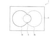
また、上記実施形態では、第1コイル状回路及び第2コイル状回路の内形が長方形から他の長方形が突出する形状の場合を説明したが、第1コイル状回路及び第2コイル状回路の内形は他の形状とすることもできる。例えば図4Aに示すように第1コイル状回路及び第2コイル状回路の内形を半径の大きい第1の円から半径の小さい第2の円が突出する形状としてもよい。また、図4Bに示すように第1コイル状回路及び第2コイル状回路の内形を略長方形の形状とし、平面視で交差するように配設してもよい。 Moreover, although the said embodiment demonstrated the case where the internal shape of a 1st coil-shaped circuit and a 2nd coil-shaped circuit was a shape where another rectangle protrudes from a rectangle, a 1st coil-shaped circuit and a 2nd coil-shaped circuit of The inner shape may be other shapes. For example, as shown in FIG. 4A, the inner shapes of the first coil-like circuit and the second coil-like circuit may be a shape in which a second circle having a small radius protrudes from a first circle having a large radius. In addition, as shown in FIG. 4B, the inner shapes of the first coil-like circuit and the second coil-like circuit may be substantially rectangular and may be arranged so as to intersect in plan view.
さらに、例えば図4Cに示すように第1コイル状回路が第2コイル状回路を平面視で囲繞するような閉ループを有さない形状とすることもできる。ワイヤレス受電用アンテナをこのように構成しても第1コイル状回路と第2コイル状回路とが平面視で重複領域を有する限り、本発明の効果を奏することができる。 Further, for example, as shown in FIG. 4C, the first coiled circuit may have a shape without a closed loop that surrounds the second coiled circuit in a plan view. Even if the wireless power receiving antenna is configured in this way, the effect of the present invention can be obtained as long as the first coiled circuit and the second coiled circuit have overlapping regions in plan view.
また、第1コイル状回路、第2コイル状回路及び第3コイル状回路が表面側から見て外側から反時計回り(左回り)に延伸する場合を用いて説明したが、延伸方向はこれに限定されるものではなく、閉ループで第1コイル状回路部分の電流方向と第2コイル状回路部分の電流方向が一致する限り、右回り又は左回りと右回りとの混在であってもよい。 Moreover, although demonstrated using the case where the 1st coil-shaped circuit, the 2nd coil-shaped circuit, and the 3rd coil-shaped circuit extend | stretch counterclockwise (counterclockwise) from the outer side seeing from the surface side, the extending | stretching direction is this It is not limited, and as long as the current direction of the first coiled circuit portion and the current direction of the second coiled circuit portion coincide with each other in a closed loop, it may be clockwise or a mixture of counterclockwise and clockwise.
また、上記実施形態では、第1コイル状回路、第2コイル状回路及び第3コイル状回路を直列に接続する場合を説明したが、用途に応じてその一部又は全部を並列に接続してもよい。 Moreover, although the said embodiment demonstrated the case where a 1st coil-shaped circuit, a 2nd coil-shaped circuit, and a 3rd coil-shaped circuit were connected in series, the one part or all part was connected in parallel according to a use. Also good.
また、当該ワイヤレス受電用アンテナにおいて、第1コイル状回路と第2コイル状回路との間及び第2コイル状回路と第2接続端子との間は、スルーホール以外の手段により接続してもよい。例えば第1コイル状回路の表面と第2コイル状回路の表面とを、絶縁層を迂回して接続するリード線等で接続してもよい。 In the wireless power receiving antenna, the first coiled circuit and the second coiled circuit and the second coiled circuit and the second connection terminal may be connected by means other than a through hole. . For example, the surface of the first coiled circuit and the surface of the second coiled circuit may be connected by a lead wire or the like that bypasses and connects the insulating layer.
また、当該ワイヤレス受電用アンテナにおいて、第3コイル状回路は必須の構成要素ではなく、省略してもよい。また、上記実施形態では、接続を容易とするためスルーホールの接続部等に中間端子を用いているが、この中間端子は一手段であって必須の構成要素ではなく、例えばコイル状回路に直接接続してもよい。 In the wireless power receiving antenna, the third coiled circuit is not an essential component and may be omitted. Further, in the above embodiment, an intermediate terminal is used for a through hole connection portion or the like for easy connection. However, this intermediate terminal is one means and is not an essential component, for example, directly on a coiled circuit. You may connect.
以上のように、本発明のワイヤレス受電用アンテナは、小型化が可能であると共に、給電用アンテナと受電用アンテナとの位置ずれが生じても電力の受信効率の低下を抑制できる。 As described above, the wireless power receiving antenna of the present invention can be miniaturized and can suppress a decrease in power reception efficiency even if a positional deviation occurs between the power feeding antenna and the power receiving antenna.
1 フレキシブルプリント配線板
2 絶縁層
3 第1コイル層
3a 第1コイル状回路
3b 第3コイル状回路
4 第2コイル層
4a 第2コイル状回路
5 閉ループ
6 第1カバーレイ
7 第2カバーレイ
8 第1接続端子
9 第2接続端子
10 配線
11 第1中間端子
12 第2中間端子
13 第3中間端子
14 スルーホール
15 カバーフィルム
16 接着層
17 開口DESCRIPTION OF
Claims (7)
Translated fromJapaneseこのフレキシブルプリント配線板が、
合成樹脂製の絶縁層と、
この絶縁層の一方側面に積層され、第1コイル状回路を有する第1コイル層と、
上記絶縁層の他方側面に積層され、第2コイル状回路を有する第2コイル層と
を備えており、
上記第1コイル状回路と上記第2コイル状回路とが平面視で重複領域を有するワイヤレス受電用アンテナ。Consists of flexible printed wiring boards,
This flexible printed circuit board
An insulating layer made of synthetic resin;
A first coil layer laminated on one side of the insulating layer and having a first coiled circuit;
A second coil layer laminated on the other side surface of the insulating layer and having a second coiled circuit,
The wireless power receiving antenna, wherein the first coiled circuit and the second coiled circuit have an overlapping region in plan view.
上記閉ループの面積の上記第1コイル状回路の面積に対する比率及び上記第2コイル状回路の面積に対する比率が0.2以上0.8以下である請求項2に記載のワイヤレス受電用アンテナ。The ratio of the area of the first coiled circuit to the area of the second coiled circuit is 0.5 or more and 2 or less,
3. The wireless power receiving antenna according to claim 2, wherein a ratio of the area of the closed loop to the area of the first coiled circuit and a ratio of the area of the second coiled circuit is 0.2 or more and 0.8 or less.
Priority Applications (1)
| Application Number | Priority Date | Filing Date | Title |
|---|---|---|---|
| JP2014148681AJP2016025502A (en) | 2014-07-22 | 2014-07-22 | Antenna for wireless power reception, and wearable device |
Applications Claiming Priority (1)
| Application Number | Priority Date | Filing Date | Title |
|---|---|---|---|
| JP2014148681AJP2016025502A (en) | 2014-07-22 | 2014-07-22 | Antenna for wireless power reception, and wearable device |
Publications (1)
| Publication Number | Publication Date |
|---|---|
| JP2016025502Atrue JP2016025502A (en) | 2016-02-08 |
Family
ID=55271916
Family Applications (1)
| Application Number | Title | Priority Date | Filing Date |
|---|---|---|---|
| JP2014148681APendingJP2016025502A (en) | 2014-07-22 | 2014-07-22 | Antenna for wireless power reception, and wearable device |
Country Status (1)
| Country | Link |
|---|---|
| JP (1) | JP2016025502A (en) |
Cited By (4)
| Publication number | Priority date | Publication date | Assignee | Title |
|---|---|---|---|---|
| CN109087798A (en)* | 2018-07-26 | 2018-12-25 | 努比亚技术有限公司 | A kind of wireless charging electric wire coil assembly |
| WO2023074699A1 (en) | 2021-10-26 | 2023-05-04 | エイターリンク株式会社 | Power-receiving antenna |
| JP2023141929A (en)* | 2022-03-24 | 2023-10-05 | 株式会社東芝 | isolator |
| JP7704471B1 (en)* | 2024-10-28 | 2025-07-08 | 株式会社ビーコンテクノロジーズ | Drowning Detection System |
Citations (12)
| Publication number | Priority date | Publication date | Assignee | Title |
|---|---|---|---|---|
| JPH10154216A (en)* | 1996-11-25 | 1998-06-09 | Matsushita Electric Ind Co Ltd | Non-contact IC card |
| JPH11272826A (en)* | 1998-03-26 | 1999-10-08 | Sony Corp | Radio receiver |
| JP2000295024A (en)* | 1999-04-06 | 2000-10-20 | Sony Corp | Non-contact tag |
| JP2004336198A (en)* | 2003-05-01 | 2004-11-25 | Toshiba Corp | Antenna device |
| JP2005218021A (en)* | 2004-02-02 | 2005-08-11 | Fujitsu Frontech Ltd | Small loop antenna for inductive reader/writer |
| JP2007523562A (en)* | 2004-02-20 | 2007-08-16 | スリーエム イノベイティブ プロパティズ カンパニー | Multiple loop antenna for radio frequency identification (RFID) communication |
| JP2009088178A (en)* | 2007-09-28 | 2009-04-23 | Tsuchiya Co Ltd | Film for noncontact electric power transmission |
| JP2009267761A (en)* | 2008-04-25 | 2009-11-12 | Alps Electric Co Ltd | Loop antenna |
| JP2010200207A (en)* | 2009-02-27 | 2010-09-09 | Nec Corp | Multiple loop antenna |
| US20110043431A1 (en)* | 2008-04-04 | 2011-02-24 | Deutsche Post Ag | Antenna arrangement having at least two decoupled antenna coils; rf component for non-contact transmission of energy and data; electronic device having rf component |
| JP2011254307A (en)* | 2010-06-02 | 2011-12-15 | Kyodo Printing Co Ltd | Antenna sheet and information recording medium |
| JP2012222961A (en)* | 2011-04-08 | 2012-11-12 | Nec Tokin Corp | Antenna module and non-contact power transmission system |
- 2014
- 2014-07-22JPJP2014148681Apatent/JP2016025502A/enactivePending
Patent Citations (12)
| Publication number | Priority date | Publication date | Assignee | Title |
|---|---|---|---|---|
| JPH10154216A (en)* | 1996-11-25 | 1998-06-09 | Matsushita Electric Ind Co Ltd | Non-contact IC card |
| JPH11272826A (en)* | 1998-03-26 | 1999-10-08 | Sony Corp | Radio receiver |
| JP2000295024A (en)* | 1999-04-06 | 2000-10-20 | Sony Corp | Non-contact tag |
| JP2004336198A (en)* | 2003-05-01 | 2004-11-25 | Toshiba Corp | Antenna device |
| JP2005218021A (en)* | 2004-02-02 | 2005-08-11 | Fujitsu Frontech Ltd | Small loop antenna for inductive reader/writer |
| JP2007523562A (en)* | 2004-02-20 | 2007-08-16 | スリーエム イノベイティブ プロパティズ カンパニー | Multiple loop antenna for radio frequency identification (RFID) communication |
| JP2009088178A (en)* | 2007-09-28 | 2009-04-23 | Tsuchiya Co Ltd | Film for noncontact electric power transmission |
| US20110043431A1 (en)* | 2008-04-04 | 2011-02-24 | Deutsche Post Ag | Antenna arrangement having at least two decoupled antenna coils; rf component for non-contact transmission of energy and data; electronic device having rf component |
| JP2009267761A (en)* | 2008-04-25 | 2009-11-12 | Alps Electric Co Ltd | Loop antenna |
| JP2010200207A (en)* | 2009-02-27 | 2010-09-09 | Nec Corp | Multiple loop antenna |
| JP2011254307A (en)* | 2010-06-02 | 2011-12-15 | Kyodo Printing Co Ltd | Antenna sheet and information recording medium |
| JP2012222961A (en)* | 2011-04-08 | 2012-11-12 | Nec Tokin Corp | Antenna module and non-contact power transmission system |
Cited By (4)
| Publication number | Priority date | Publication date | Assignee | Title |
|---|---|---|---|---|
| CN109087798A (en)* | 2018-07-26 | 2018-12-25 | 努比亚技术有限公司 | A kind of wireless charging electric wire coil assembly |
| WO2023074699A1 (en) | 2021-10-26 | 2023-05-04 | エイターリンク株式会社 | Power-receiving antenna |
| JP2023141929A (en)* | 2022-03-24 | 2023-10-05 | 株式会社東芝 | isolator |
| JP7704471B1 (en)* | 2024-10-28 | 2025-07-08 | 株式会社ビーコンテクノロジーズ | Drowning Detection System |
Similar Documents
| Publication | Publication Date | Title |
|---|---|---|
| JP6286800B2 (en) | Printed wiring board, antenna and wireless power feeder | |
| JP6365933B2 (en) | Flexible printed wiring board, antenna and wireless power feeder | |
| CN108184333B (en) | Combined antenna module | |
| CN108140950B (en) | Antenna unit and wireless power transmission module comprising same | |
| CN108461893B (en) | Antenna device and portable terminal including the same | |
| CN206516763U (en) | Antenna device and electronic equipment | |
| US11282639B2 (en) | Antenna device and electronic apparatus | |
| WO2013121729A1 (en) | Contactless charging module and mobile terminal provided with same | |
| JPWO2017038797A1 (en) | Flexible printed wiring board and non-contact charging system | |
| CN106898474A (en) | Coil block | |
| US20190252768A1 (en) | Antenna module and electronic device having the same | |
| US10186875B2 (en) | Coil type unit for wireless power transmission, wireless power transmission device, electronic device and manufacturing method of coil type unit for wireless power transmission | |
| WO2019111848A1 (en) | Coil module | |
| JP2016025502A (en) | Antenna for wireless power reception, and wearable device | |
| JP7103569B2 (en) | Flexible printed wiring board | |
| JP6384747B2 (en) | Flexible printed wiring board for wireless communication devices | |
| WO2017047498A1 (en) | Flexible printed wiring board and contactless charging system | |
| KR20160121279A (en) | multi antenna unit and wireless charging module having the same | |
| CN116547768A (en) | Coil and electrical system including the coil | |
| KR102014378B1 (en) | Antenna module and electronic device having the same | |
| KR102014387B1 (en) | Antenna module and electronic device having the same | |
| JP2018006480A (en) | Planar coil element and wireless power supply device | |
| JP2018160599A (en) | Planar coil element | |
| KR102339683B1 (en) | Heat radiation unit for a wireless charging and wireless charging module having the same | |
| KR20200034546A (en) | Antenna module |
Legal Events
| Date | Code | Title | Description |
|---|---|---|---|
| A625 | Written request for application examination (by other person) | Free format text:JAPANESE INTERMEDIATE CODE: A625 Effective date:20170323 | |
| A977 | Report on retrieval | Free format text:JAPANESE INTERMEDIATE CODE: A971007 Effective date:20180308 | |
| A131 | Notification of reasons for refusal | Free format text:JAPANESE INTERMEDIATE CODE: A131 Effective date:20180320 | |
| A02 | Decision of refusal | Free format text:JAPANESE INTERMEDIATE CODE: A02 Effective date:20180918 |