JP2016025316A - Illumination optical system, lighting system, and illumination optical element - Google Patents
Illumination optical system, lighting system, and illumination optical elementDownload PDFInfo
- Publication number
- JP2016025316A JP2016025316AJP2014150901AJP2014150901AJP2016025316AJP 2016025316 AJP2016025316 AJP 2016025316AJP 2014150901 AJP2014150901 AJP 2014150901AJP 2014150901 AJP2014150901 AJP 2014150901AJP 2016025316 AJP2016025316 AJP 2016025316A
- Authority
- JP
- Japan
- Prior art keywords
- illumination
- illumination optical
- light
- optical system
- optical element
- Prior art date
- Legal status (The legal status is an assumption and is not a legal conclusion. Google has not performed a legal analysis and makes no representation as to the accuracy of the status listed.)
- Granted
Links
- 230000003287optical effectEffects0.000titleclaimsabstractdescription294
- 238000005286illuminationMethods0.000titleclaimsabstractdescription250
- 238000000034methodMethods0.000abstractdescription7
- 238000009826distributionMethods0.000description31
- 238000010586diagramMethods0.000description14
- 241000276498Pollachius virensSpecies0.000description3
- 230000000694effectsEffects0.000description3
- 230000004907fluxEffects0.000description3
- 238000003384imaging methodMethods0.000description3
- 239000004973liquid crystal related substanceSubstances0.000description3
- 239000000463materialSubstances0.000description3
- 230000004048modificationEffects0.000description3
- 238000012986modificationMethods0.000description3
- 230000005540biological transmissionEffects0.000description2
- 238000005520cutting processMethods0.000description2
- 210000001747pupilAnatomy0.000description2
- 238000012935AveragingMethods0.000description1
- VYPSYNLAJGMNEJ-UHFFFAOYSA-NSilicium dioxideChemical compoundO=[Si]=OVYPSYNLAJGMNEJ-UHFFFAOYSA-N0.000description1
- 230000008901benefitEffects0.000description1
- 230000008859changeEffects0.000description1
- 239000013078crystalSubstances0.000description1
- 230000002542deteriorative effectEffects0.000description1
- 239000011521glassSubstances0.000description1
- 229910052736halogenInorganic materials0.000description1
- 150000002367halogensChemical class0.000description1
- 230000001678irradiating effectEffects0.000description1
- 238000004519manufacturing processMethods0.000description1
- 239000004033plasticSubstances0.000description1
- 239000004065semiconductorSubstances0.000description1
- 239000002699waste materialSubstances0.000description1
Images


Classifications
- G—PHYSICS
- G02—OPTICS
- G02B—OPTICAL ELEMENTS, SYSTEMS OR APPARATUS
- G02B19/00—Condensers, e.g. light collectors or similar non-imaging optics
- G02B19/0004—Condensers, e.g. light collectors or similar non-imaging optics characterised by the optical means employed
- G02B19/0009—Condensers, e.g. light collectors or similar non-imaging optics characterised by the optical means employed having refractive surfaces only
- G—PHYSICS
- G02—OPTICS
- G02B—OPTICAL ELEMENTS, SYSTEMS OR APPARATUS
- G02B21/00—Microscopes
- G02B21/06—Means for illuminating specimens
- G02B21/08—Condensers
- G—PHYSICS
- G02—OPTICS
- G02B—OPTICAL ELEMENTS, SYSTEMS OR APPARATUS
- G02B27/00—Optical systems or apparatus not provided for by any of the groups G02B1/00 - G02B26/00, G02B30/00
- G02B27/09—Beam shaping, e.g. changing the cross-sectional area, not otherwise provided for
- G02B27/0905—Dividing and/or superposing multiple light beams
- G—PHYSICS
- G02—OPTICS
- G02B—OPTICAL ELEMENTS, SYSTEMS OR APPARATUS
- G02B27/00—Optical systems or apparatus not provided for by any of the groups G02B1/00 - G02B26/00, G02B30/00
- G02B27/09—Beam shaping, e.g. changing the cross-sectional area, not otherwise provided for
- G02B27/0938—Using specific optical elements
- G02B27/095—Refractive optical elements
- G02B27/0972—Prisms
- G—PHYSICS
- G02—OPTICS
- G02B—OPTICAL ELEMENTS, SYSTEMS OR APPARATUS
- G02B3/00—Simple or compound lenses
- G02B3/02—Simple or compound lenses with non-spherical faces
- G02B3/08—Simple or compound lenses with non-spherical faces with discontinuous faces, e.g. Fresnel lens
- G—PHYSICS
- G02—OPTICS
- G02B—OPTICAL ELEMENTS, SYSTEMS OR APPARATUS
- G02B5/00—Optical elements other than lenses
- G02B5/04—Prisms
- G02B5/045—Prism arrays
Landscapes
- Physics & Mathematics (AREA)
- General Physics & Mathematics (AREA)
- Optics & Photonics (AREA)
- Chemical & Material Sciences (AREA)
- Analytical Chemistry (AREA)
- Microscoopes, Condenser (AREA)
- Engineering & Computer Science (AREA)
- General Engineering & Computer Science (AREA)
- Exposure And Positioning Against Photoresist Photosensitive Materials (AREA)
- Exposure Of Semiconductors, Excluding Electron Or Ion Beam Exposure (AREA)
Abstract
Translated fromJapaneseDescription
Translated fromJapanese本発明は、被照明面を面状に照明する照明光学素子を備えた照明光学系、及び、照明装置、さらに、被照明面を面状に照明する照明光学素子に関する。 The present invention relates to an illumination optical system including an illumination optical element that illuminates a surface to be illuminated in a plane, an illumination device, and an illumination optical element that illuminates a surface to be illuminated in a plane.
顕微鏡や半導体露光装置の分野では、標本面を均一に照明するために、ケーラー照明が一般的に採用されている。しかしながら、ケーラー照明では、光源から出射される光量が出射角度に依存する特性(以降、配光特性と記す。)に起因した照明の不均一が生じてしまう。このため、フライアイレンズを用いることで、ケーラー照明における配光特性に起因する照明の不均一を抑制する技術が提案されている。このような技術は、例えば、特許文献1に記載されている。 In the field of microscopes and semiconductor exposure apparatuses, Koehler illumination is generally employed to uniformly illuminate the specimen surface. However, in Koehler illumination, illumination nonuniformity occurs due to a characteristic in which the amount of light emitted from the light source depends on the emission angle (hereinafter referred to as a light distribution characteristic). For this reason, the technique which suppresses the nonuniformity of the illumination resulting from the light distribution characteristic in Koehler illumination by using a fly eye lens is proposed. Such a technique is described in
ところで、フライアイレンズを用いて配光特性に起因する照明の不均一を抑制するためには、フライアイレンズに加えて、フライアイレンズにより形成された複数の光源像からの光を被照明面の同一の領域内に重ねて照射するためのレンズが必要である。
以上のような実情を踏まえ、本発明は、光源に起因する照明の不均一を少ない光学素子で抑制する技術を提供することを課題とする。By the way, in order to suppress nonuniform illumination caused by light distribution characteristics using a fly-eye lens, in addition to the fly-eye lens, light from a plurality of light source images formed by the fly-eye lens is illuminated. A lens for overlapping and irradiating in the same region.
In light of the above circumstances, it is an object of the present invention to provide a technique for suppressing nonuniform illumination caused by a light source with a small number of optical elements.
本発明の第1の態様は、被照明面の所定領域に光を面状に照射する照明光学素子を備えた照明光学系であって、前記照明光学素子は、前記被照明面に向けられる光学面を有し、前記光学面は、光軸に直交する直交方向に、それぞれ光を前記所定領域に向けて屈折させる、前記所定領域によって定まる一定のピッチで形成された複数の屈折面を有する照明光学系を提供する。 According to a first aspect of the present invention, there is provided an illumination optical system including an illumination optical element that irradiates light onto a predetermined area of a surface to be illuminated in a planar shape, and the illumination optical element is optically directed toward the surface to be illuminated. The optical surface has a plurality of refracting surfaces formed at a constant pitch determined by the predetermined region, each of which refracts light toward the predetermined region in a direction orthogonal to the optical axis. An optical system is provided.
本発明の第2の態様は、第1の態様に記載の照明光学系において、前記複数の屈折面は、前記光軸に沿った断面において、前記光軸となす角度が異なる直線形状を有し、前記光軸に近い屈折面ほど、前記光軸に沿った断面において、前記光軸と大きな角度をなす照明光学系を提供する。 According to a second aspect of the present invention, in the illumination optical system according to the first aspect, the plurality of refracting surfaces have a linear shape with different angles to the optical axis in a cross section along the optical axis. Provided is an illumination optical system in which a refractive surface closer to the optical axis forms a larger angle with the optical axis in a cross section along the optical axis.
本発明の第3の態様は、第1の態様または第2の態様に記載の照明光学系において、前記光学面は、さらに、前記複数の屈折面よりも前記直交方向に前記光軸から離れた位置に、それぞれ光を前記所定領域の一部に向けて屈折させる複数の第2の屈折面を有する照明光学系を提供する。 According to a third aspect of the present invention, in the illumination optical system according to the first aspect or the second aspect, the optical surface is further away from the optical axis in the orthogonal direction than the plurality of refractive surfaces. Provided is an illumination optical system having a plurality of second refracting surfaces that refract light at a position toward a part of the predetermined region.
本発明の第4の態様は、第3の態様に記載の照明光学系において、前記複数の第2の屈折面は、前記光軸に沿った前記断面において、前記光軸と異なる角度をなす直線形状を有し、前記光軸に近い第2の屈折面ほど、前記光軸に沿った前記断面において、前記光軸と大きな角度をなす照明光学系を提供する。 According to a fourth aspect of the present invention, in the illumination optical system according to the third aspect, the plurality of second refracting surfaces are straight lines having an angle different from the optical axis in the cross section along the optical axis. Provided is an illumination optical system that has a shape and has a larger angle with the optical axis in the cross section along the optical axis, as the second refractive surface is closer to the optical axis.
本発明の第5の態様は、第3の態様又は第4の態様に記載の照明光学系において、前記複数の第2の屈折面は、前記直交方向に、前記複数の屈折面が形成されるピッチよりも短い一定のピッチで形成される照明光学系を提供する。 According to a fifth aspect of the present invention, in the illumination optical system according to the third aspect or the fourth aspect, the plurality of second refracting surfaces are formed in the orthogonal direction. Provided is an illumination optical system formed at a constant pitch shorter than the pitch.
本発明の第6の態様は、第1の態様乃至第5の態様のいずれか1つに記載の照明光学系において、前記照明光学素子は、前記光学面とは反対側に、第2の光学面を有し、前記第2の光学面は、フレネル面である照明光学系を提供する。 According to a sixth aspect of the present invention, in the illumination optical system according to any one of the first to fifth aspects, the illumination optical element is disposed on the side opposite to the optical surface, the second optical element. The illumination optical system has a surface, and the second optical surface is a Fresnel surface.
本発明の第7の態様は、第1の態様乃至第6の態様のいずれか1つに記載の照明光学系において、前記複数の屈折面の各々の前記直交方向の幅は、前記所定領域の前記直交方向の幅に等しい照明光学系を提供する。 According to a seventh aspect of the present invention, in the illumination optical system according to any one of the first to sixth aspects, a width of each of the plurality of refractive surfaces in the orthogonal direction is the predetermined region. An illumination optical system having a width equal to the width in the orthogonal direction is provided.
本発明の第8の態様は、第3の態様乃至第5の態様のいずれか1つに記載の照明光学系において、さらに、前記照明光学素子に入射する光の光束径を可変する可変絞りを備える照明光学系を提供する。 According to an eighth aspect of the present invention, there is provided the illumination optical system according to any one of the third to fifth aspects, further comprising a variable stop for changing a light beam diameter of light incident on the illumination optical element. Provided is an illumination optical system.
本発明の第9の態様は、第1の態様乃至第8の態様のいずれか1つに記載の照明光学系を備える照明装置を提供する。 According to a ninth aspect of the present invention, there is provided an illumination device including the illumination optical system according to any one of the first to eighth aspects.
本発明の第10の態様は、被照明面の所定領域に光を面状に照射する照明光学素子であって、前記被照明面に向けられる光学面を有し、前記光学面は、光軸に直交する直交方向に、それぞれ光を前記所定領域に向けて屈折させる前記直交方向に、前記所定領域によって定まる一定のピッチで形成される複数の屈折面を有する照明光学素子を提供する。 A tenth aspect of the present invention is an illumination optical element that irradiates a predetermined region of a surface to be illuminated with light in a planar shape, and has an optical surface directed to the surface to be illuminated, the optical surface having an optical axis There is provided an illumination optical element having a plurality of refracting surfaces formed at a constant pitch determined by the predetermined region in the orthogonal direction in which light is refracted toward the predetermined region.
本発明によれば、光源に起因する照明の不均一を少ない光学素子で抑制する技術を提供することができる。 ADVANTAGE OF THE INVENTION According to this invention, the technique which suppresses the nonuniformity of the illumination resulting from a light source with few optical elements can be provided.
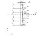
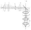
図1は、本実施例に係る照明装置10の構成を例示した図である。図2は、本実施例に係る照明光学素子3を例示した図である。図3は、本実施例に係る照明装置10の各面における照明光の光量分布を例示した図である。 FIG. 1 is a diagram illustrating a configuration of a
照明装置10は、被照明面である標本面SPの領域A1を面状に照明する装置である。照明装置10は、図1に示すように、照明光を出射する光源1と、照明光学系10aと、を備えている。照明光学系10aは、光源1からの光を標本面SPの領域A1に面状に照射する光学系であり、コレクタレンズ2と、照明光学素子3と、を備えている。 The
光源1は、例えば、ハロゲンランプなどのランプ光源である。光源1は、図3(a)に示すような配光特性を有している。図3(a)の横軸θは、光軸AXに対する出射角である。図3(a)に示されるように、光源1は光軸AXに対しておよそ対称な配光特性を有していて、出射角によって異なる光量の照明光が光源1から放射される。なお、光源1は、ランプ光源に限られず、LED光源など他の光源であってもよい。 The
コレクタレンズ2は、光源1から出射した光をコリメートして、平行光束として照明光学素子3に入射させる。これにより、光源1から出射する光の角度方向の光量分布(図3(a)参照)は、照明光学素子3に入射する光の光束径方向の光量分布(図3(b)参照)に変換される。図3(b)の横軸Xは、図2に示すX方向の位置である。 The
照明光学素子3は、平行光束として入射した光を標本面SP(被照明面)の領域A1に面状に照射する光学素子である。照明光学素子3の材料は、例えば、ガラス、プラスチック、結晶材料(例えば、石英ガラス)などである。照明光学素子3は、標本面SPに向けられる光学面S1を有し、さらに、光学面S1とは反対側に、第2の光学面である光学面S2を有している。 The illumination
光学面S2は、光軸AXと直交する平面である。一方、光学面S1は、図2に示すように、光軸AXに直交する方向(例えば、図1に示すX方向。以降、直交方向と記す)に、それぞれ光を領域A1に向けて屈折させる複数の屈折面RSを有している。 The optical surface S2 is a plane orthogonal to the optical axis AX. On the other hand, as shown in FIG. 2, the optical surface S1 refracts light toward the region A1 in a direction orthogonal to the optical axis AX (for example, the X direction shown in FIG. 1, hereinafter referred to as the orthogonal direction). It has a plurality of refractive surfaces RS.
複数の屈折面RSは、直交方向に一定のピッチPで形成されている。このピッチP(つまり、複数の屈折面RSの各々の直交方向の幅)が領域A1の直交方向の幅D1になる。さらに、複数の屈折面RSは、光軸AXに沿った断面(例えば、XZ断面)において、光軸AXとなす角度(角度θ0≠θ1≠θ2)が異なる直線形状を有している。そして、光軸AXに近い屈折面RSほど、光軸AXに沿った断面において、光軸AXと大きな角度をなしている(θ0>θ1>θ2)。なお、図2では、照明光学素子3は、屈折面RSが形成される各領域の最大厚さtが一定となるように構成されている。このため、照明光学素子3には、光軸AXに遠いほど、屈折面RSによって深い溝が形成されている。 The plurality of refractive surfaces RS are formed at a constant pitch P in the orthogonal direction. This pitch P (that is, the width in the orthogonal direction of each of the plurality of refractive surfaces RS) becomes the width D1 in the orthogonal direction of the region A1. Further, the plurality of refractive surfaces RS have linear shapes with different angles (angles θ0 ≠ θ1 ≠ θ2) with the optical axis AX in a cross section (for example, XZ cross section) along the optical axis AX. The refractive surface RS closer to the optical axis AX forms a larger angle with the optical axis AX in the cross section along the optical axis AX (θ0> θ1> θ2). In FIG. 2, the illumination
照明光学素子3に平行光束として入射した光は、光学面S2を透過して光学面S1に入射し、光学面S1において入射した屈折面RS毎に分割される。なお、分割された光は、それぞれピッチPの光束径を有する平行光束であり、図3(b)に示すように、それぞれ光源1における異なる出射角範囲に対応する異なる光量分布を有している。 The light that has entered the illumination
その後、分割された光の各々は、各屈折面RSで領域A1に向けて屈折し、平行光束のままで領域A1に入射する。即ち、照明光学素子3で所定の出射角範囲毎に分割された光は、図3(c)に示すように、領域A1で重なり合う。これにより、配光特性に起因する不均一な光量分布が標本面SP(領域A1)において平均化される。なお、図3(c)は、標本面SPにおける光量分布を示している。 Thereafter, each of the divided lights is refracted toward the area A1 by each refracting surface RS, and enters the area A1 as a parallel light flux. That is, the light divided for each predetermined emission angle range by the illumination
本実施例によれば、光源1の配光特性に起因する照明の不均一を抑制することができる。従って、標本面SP(被照明面)を均一に照明することができる。さらに、本実施例によれば、従来に比べて少ない光学素子で容易に、光源1の配光特性に起因する照明の不均一を抑制することができる。この点について以下で詳細に説明する。 According to the present embodiment, it is possible to suppress uneven illumination due to the light distribution characteristics of the
図4は、フライアイレンズ4を備えた従来の照明装置の構成を例示した図である。フライアイレンズ4は、光源から出射した光を所定の出射角範囲毎に分割する点については照明光学素子3と同様である。ただし、フライアイレンズ4は、照明光学素子3とは異なり、分割した光の各々を集光して複数の光源像1aを形成する。このため、フライアイレンズ4を備えた従来の照明装置には、フライアイレンズ4に加えて、フライアイレンズ4が形成した複数の光源像1aからの光をそれぞれ標本面SPに照射してケーラー照明を行うためのコンデンサレンズ5が必要となる。 FIG. 4 is a diagram illustrating a configuration of a conventional lighting device including the fly-eye lens 4. The fly-eye lens 4 is the same as the illumination
これに対して、照明光学素子3は、分割した光を集光することなく、そのまま標本面SPに照射する。これにより、照明光学素子3は、フライアイレンズ4とコンデンサレンズ5の両方の機能を同時に実現している。このため、本実施例によれば、従来に比べて少ない光学素子で、光源1の配光特性に起因する照明の不均一を抑制して、標本面SP(被照明面)を均一に照明することができる。 On the other hand, the illumination
また、フライアイレンズは、一般に一枚で使用されるものではなく、二枚並べて使用される。そして、高い照明の均一性を実現するためには、一方のフライアイレンズは他方のフライアイレンズに対して精度良く配置する必要がある。 Further, the fly-eye lens is not generally used as a single lens, but is used in a line. In order to achieve high illumination uniformity, one fly-eye lens needs to be accurately arranged with respect to the other fly-eye lens.
これに対して、照明光学素子3の配置には、フライアイレンズの配置のような高い精度は要求されない。このため、照明光学素子3を備える本実施例に係る照明光学系10a及び照明装置10によれば、従来の照明装置よりも容易に照明の不均一を抑制することができる。 On the other hand, the arrangement of the illumination
さらに、照明光学素子3は、屈折面RSの断面形状が直線状であることから、材料を切削することで容易に作製することができる。なお、照明光学素子3は、型を使って作製されてもよい。この場合、切削により照明光学素子3の型を容易に作製することができる。 Furthermore, the illumination
図2に示す照明光学素子3は、光軸AX上に光軸AXと直交する屈折面RSを有しているが、照明光学素子はこの構成に限定されない。照明光学素子は、図5に示す変形例に係る照明光学素子6のように、光軸AXが屈折面RS間の境界を通り、光軸AXに接する屈折面RSが光軸AXと直交する面に対して傾斜するように、構成されてもよい。 The illumination
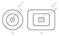
また、光源の配光特性が光軸に対して対称である場合には、照明光学素子も対称な形状であることが望ましい。図6(a)は、照明光学素子3を光軸AXに沿った方向から見た図である。照明装置10で照明した標本面SPを接眼レンズなどで観察する場合には、照明光学素子は、図6(a)に示す照明光学素子3のように、光軸AXを中心にしておよそ点対称な形状(ここでは、円形)であることが望ましい。図6(b)は、照明光学素子3の変形例である照明光学素子7を光軸AXに沿った方向から見た図である。標本面SPをカメラなどで撮像する場合には、照明光学素子は、図6(b)に示す照明光学素子7のように、撮像素子の形状に合わせた形状であることが望ましく、光軸AXを含む基準線に対しておよそ線対称な形状(ここでは、矩形)であることが望ましい。 Further, when the light distribution characteristic of the light source is symmetric with respect to the optical axis, it is desirable that the illumination optical element also has a symmetric shape. FIG. 6A is a view of the illumination
一般に照明装置に求められる開口数(NA)は、観察倍率に依存している。例えば、観察倍率が10倍であれば0.4程度のNAが、観察倍率が20倍であれば0.7程度のNAが、観察倍率が40倍であれば0.95程度のNAが、照明装置に要求される。観察倍率が高くなればなるほど、照明すべき領域は小さくなるため、要求されるNAが高いほど照明領域も小さくてすむ。本実施例は、この点に着目したものであり、光源の配光特性に起因する照明の不均一を抑制しつつ、広い観察倍率に対応できる照明を実現するというものである。 In general, the numerical aperture (NA) required for the illumination device depends on the observation magnification. For example, if the observation magnification is 10, the NA is about 0.4, if the observation magnification is 20, the NA is about 0.7, and if the observation magnification is 40, the NA is about 0.95. Required for lighting equipment. The higher the observation magnification, the smaller the area to be illuminated. Therefore, the higher the required NA, the smaller the illumination area. The present embodiment pays attention to this point, and realizes illumination that can cope with a wide observation magnification while suppressing uneven illumination due to light distribution characteristics of a light source.
図7は、本実施例に係る照明光学素子8の構成を例示した図である。なお、本実施例に係る照明光学系及び照明装置は、照明光学素子3の代わりに照明光学素子8を含む点を除き、実施例1に係る照明光学系10a及び照明装置10と同様である。照明光学素子8は、光学面S1が、複数の屈折面RSに加えて、複数の屈折面RS2と複数の屈折面RS3を有している点が、照明光学素子3とは異なっている。ここでは、照明光学素子8の屈折面RS、屈折面RS2、屈折面RS3が、それぞれ、10倍観察用、20倍観察用、40倍観察用の照明を形成する例について説明する。 FIG. 7 is a diagram illustrating the configuration of the illumination
複数の屈折面RSは、照明光学素子3の複数の屈折面RSと同様である。複数の屈折面RSのピッチPは、10倍の観察で照明すべき領域A1の直交方向の幅D1と同じである。最も光軸AXから離れた屈折面RSは、その屈折面RSで屈折した光が領域A1にNA0.4で入射するように傾斜している。 The plurality of refractive surfaces RS are the same as the plurality of refractive surfaces RS of the illumination
複数の第2の屈折面である複数の屈折面RS2は、直交方向に複数の屈折面RSよりも光軸AXから離れた位置に形成されていて、それぞれ光を領域A1の一部(領域A2)に向けて屈折させるように構成されている。なお、複数の屈折面RS2は、光軸AXに沿った断面において光軸AXとなす角度が異なる直線形状を有している点、光軸AXに近い屈折面RS2ほど光軸AXに沿った断面において光軸AXと大きな角度をなしている点は、複数の屈折面RSと同様である。 The plurality of refracting surfaces RS2, which are the plurality of second refracting surfaces, are formed at positions farther from the optical axis AX than the plurality of refracting surfaces RS in the orthogonal direction. ). The plurality of refracting surfaces RS2 have linear shapes with different angles to the optical axis AX in the section along the optical axis AX, and the section along the optical axis AX as the refractive surface RS2 is closer to the optical axis AX. Is the same as the plurality of refractive surfaces RS in that it forms a large angle with the optical axis AX.
複数の屈折面RS2は、直交方向に複数の屈折面RSが形成されるピッチPよりも短い一定のピッチP1で形成される点が、複数の屈折面RSと異なっている。ピッチP1は、20倍の観察で照明すべき領域A2の直交方向の幅D2と同じである。最も光軸AXから離れた屈折面RS2は、その屈折面RS2で屈折した光が領域A2にNA0.7で入射するように傾斜している。 The plurality of refracting surfaces RS2 are different from the plurality of refracting surfaces RS in that they are formed at a constant pitch P1 shorter than the pitch P at which the plurality of refracting surfaces RS are formed in the orthogonal direction. The pitch P1 is the same as the width D2 in the orthogonal direction of the region A2 to be illuminated by 20 times observation. The refracting surface RS2 farthest from the optical axis AX is inclined so that light refracted by the refracting surface RS2 enters the region A2 with NA 0.7.
複数の第3の屈折面である複数の屈折面RS3は、直交方向に複数の屈折面RS2よりも光軸AXから離れた位置に形成されていて、それぞれ光を領域A2の一部(領域A3)に向けて屈折させるように構成されている。なお、複数の屈折面RS3は、光軸AXに沿った断面において光軸AXとなす角度が異なる直線形状を有している点、光軸AXに近い屈折面RS3ほど光軸AXに沿った断面において光軸AXと大きな角度をなしている点は、複数の屈折面RS、複数の屈折面RS2と同様である。 The plurality of refracting surfaces RS3, which are the plurality of third refracting surfaces, are formed at positions farther from the optical axis AX than the plurality of refracting surfaces RS2 in the orthogonal direction. ). The plurality of refracting surfaces RS3 have a linear shape with different angles to the optical axis AX in the cross section along the optical axis AX, and the refractive surface RS3 closer to the optical axis AX has a cross section along the optical axis AX. In FIG. 5, the angle with the optical axis AX is the same as the plurality of refracting surfaces RS and the plurality of refracting surfaces RS2.
複数の屈折面RS3は、直交方向に複数の屈折面RS2が形成されるピッチP1よりも短い一定のピッチP2で形成される点が、複数の屈折面RS、複数の屈折面RS2と異なっている。ピッチP2は、40倍の観察で照明すべき領域A3の直交方向の幅D3と同じである。最も光軸AXから離れた屈折面RS3は、その屈折面RS3で屈折した光が領域A3にNA0.95で入射するように傾斜している。 The plurality of refracting surfaces RS3 are different from the plurality of refracting surfaces RS and the plurality of refracting surfaces RS2 in that they are formed at a constant pitch P2 shorter than the pitch P1 at which the plurality of refracting surfaces RS2 are formed in the orthogonal direction. . The pitch P2 is the same as the width D3 in the orthogonal direction of the region A3 to be illuminated by 40 times observation. The refracting surface RS3 farthest from the optical axis AX is inclined so that light refracted by the refracting surface RS3 enters the region A3 with NA 0.95.
本実施例でも、照明光学素子8で所定の出射角範囲毎に分割された光が標本面SPで重なり合う。このため、実施例1と同様に、光源の配光特性に起因する照明の不均一を、従来に比べて少ない光学素子で容易に抑制することができる。さらに、本実施例によれば、10倍から40倍までの広い観察倍率に対応した照明を行うことができる。この点について以下で具体的に説明する。 Also in the present embodiment, the light divided for each predetermined emission angle range by the illumination
10倍で標本を観察する場合について考える。観察対象範囲である領域A1に入射した光のうちNA0.4を越える光は、10倍用の対物レンズなどの観察光学系でケラレてしまう。このため、NA0.4以内の光で観察像が形成される。従って、NA0.4を超える光(NA0.7の光やNA0.95の光など)に起因する領域A1内における照明の不均一は、観察されない。 Consider the case of observing a specimen at 10 times. Of the light that has entered the region A1 that is the observation target range, light that exceeds NA 0.4 is vignetted by an observation optical system such as a 10 × objective lens. For this reason, an observation image is formed with light within NA 0.4. Therefore, non-uniform illumination in the region A1 due to light exceeding NA 0.4 (such as NA 0.7 light or NA 0.95 light) is not observed.
20倍で標本を観察する場合について考える。観察対象範囲である領域A2に入射した光のうちNA0.7を越える光は、20倍用の対物レンズなどの観察光学系でケラレてしまう。このため、領域A2を均一に照明しているNA0.7以内の光(NA0.4の光、NA0.7の光など)で観察像が形成される。従って、NA0.7を超える光(NA0.95の光など)に起因する領域A2内における照明の不均一は、観察されない。 Consider the case of observing a specimen at 20 times. Of the light incident on the region A2 that is the observation target range, the light exceeding NA 0.7 is vignetted by an observation optical system such as a 20 × objective lens. Therefore, an observation image is formed with light within NA 0.7 (light of NA 0.4, light of NA 0.7, etc.) that uniformly illuminates the region A2. Therefore, the illumination non-uniformity in the area A2 caused by light exceeding NA 0.7 (such as light having NA 0.95) is not observed.
40倍で標本を観察する場合について考える。観察対象範囲である領域A3に入射する光は、屈折面RSで屈折した領域A1を均一に照明するNA0.4以内の光、屈折面RS2で屈折した照明される領域A2を均一に照明するNA0.7以内の光、屈折面RS3で屈折したA3を均一に照明するNA0.7を越える光である。従って、領域A3は、これらの光によって均一に照明されるため、照明の不均一は観察されない。
このように、本実施例では、いずれの観察倍率であっても照明の不均一が観察されない、広い観察倍率に対応した照明が実現される。Consider the case of observing a specimen at 40 times. The light incident on the observation target area A3 is light within NA 0.4 that uniformly illuminates the area A1 refracted by the refractive surface RS, and NA0 that uniformly illuminates the illuminated area A2 that is refracted by the refractive surface RS2. .7 or less, light exceeding NA 0.7 that uniformly illuminates A3 refracted by the refractive surface RS3. Therefore, since the area A3 is uniformly illuminated by these lights, the illumination non-uniformity is not observed.
Thus, in the present embodiment, illumination corresponding to a wide observation magnification is realized in which illumination nonuniformity is not observed at any observation magnification.
なお、本実施例に係る照明光学系及び照明装置は、図8に示すように、照明光学素子8の前側(入射側)に、照明光学素子8に入射する光の光束径を可変するための可変絞り9を備えてもよい。可変絞り9は、照明光学素子8の近傍に配置されることが望ましい。可変絞り9で照明光学素子8に入射する光の光束径を可変すると、照明光学素子8から出射する光の開口数が変化するため、可変絞り9は、開口絞りとして機能する。可変絞り9は、例えば、開口数を抑えて標本像のコントラストを改善する場合などに使用され得る。 As shown in FIG. 8, the illumination optical system and the illumination apparatus according to the present embodiment are for changing the beam diameter of light incident on the illumination
図9は、本実施例に係る照明装置20の構成を例示した図である。照明装置20は、照明光学系10a(コレクタレンズ2及び照明光学素子3)の代わりに、照明光学素子21を備えている点が、実施例1に係る照明装置10と異なっている。なお、本実施例では、照明光学素子21は、光源1からの光を標本面SPの領域A1に面状に照射する照明光学系として機能する。 FIG. 9 is a diagram illustrating the configuration of the
照明光学素子21は、光源側の光学面である光学面S2が、フレネル面として形成されている点が、実施例1に係る照明光学素子3とは異なっている。その他の点については、照明光学素子3と同様である。 The illumination
照明装置20では、照明光学素子21に入射した光は、フレネル面である光学面S2で平行光束に変換されて、光学面S1に入射する。つまり、光学面S2が照明装置10のコレクタレンズ2と同様に機能する。 In the illuminating
本実施例によっても、実施例1と同様に、光源1の配光特性に起因する照明の不均一を、従来に比べて少ない光学素子で容易に抑制することができる。さらに、本実施例によれば、コレクタレンズ2も省略することができるため、実施例1よりも少ない光学素子で照明の不均一を抑制することができる。このため、照明光学系及び照明装置全体をより安価且つコンパクトに製造することが可能となる。 Also in the present embodiment, similarly to the first embodiment, it is possible to easily suppress nonuniform illumination caused by the light distribution characteristics of the
図10は、本実施例に係る顕微鏡30の構成を例示した図である。顕微鏡30は、図示しない観察光学系を備える点、並びに、照明光学素子3と標本面SPの間に、照明光学素子3側から順に、視野絞り31、視野絞り投影レンズ(以降、FS投影レンズと記す)32、ダイクロイックミラー33、及び、対物レンズ34を備える点が、実施例1に係る照明装置10と異なっている。なお、顕微鏡30は、図10に図示される構成によって標本を照明する機能を有するという点において、照明装置である。また、本実施例では、コレクタレンズ2、照明光学素子3、視野絞り31、FS投影レンズ32、ダイクロイックミラー33、及び、対物レンズ34が、光源1からの光を標本面SPの領域に面状に照射する照明光学系30aとして機能する。 FIG. 10 is a diagram illustrating the configuration of the
視野絞り31は、標本面SPと光学的に共役な面に配置された径を可変することができる可変絞りである。FS投影レンズ32と対物レンズ34によって、視野絞り31と標本面SPの共役関係が形成されている。視野絞り31の径を可変することで、光源1からの光が照射される標本面SP上の領域の大きさを変更することができる。ダイクロイックミラー33は、照明光路と観察光路を分岐させる光学素子である。ダイクロイックミラー33の代わりにハーフミラーが用いられてもよい。 The
顕微鏡30では、照明光学素子3は、標本面SPに光を直接照射するのではなく、標本面SPと光学的に共役な面に配置された視野絞り31に光を照射する。即ち、視野絞り31が配置された標本面SPと光学的に共役な面は、照明光学素子3にとって被照明面である。 In the
本実施例によっても、実施例1と同様に、光源1の配光特性に起因する照明の不均一を、従来に比べて少ない光学素子で容易に抑制することができる。さらに、本実施例によれば、被照明面(視野絞り31の面)が拡大又は縮小されて標本面SPに投影されるため、標本面SP上での照明領域の大きさを照明光学素子3の屈折面RSのピッチPとは異なる大きさにすることができる。 Also in the present embodiment, similarly to the first embodiment, it is possible to easily suppress nonuniform illumination caused by the light distribution characteristics of the
なお、図10では、照明光学素子3が顕微鏡30の落射照明手段を構成する例を示したが、照明光学素子3は、コンデンサレンズを介して標本面SPを照明する透過透明手段を構成してもよい。 FIG. 10 shows an example in which the illumination
図11は、本実施例に係る顕微鏡40の構成を例示した図である。図12は、顕微鏡40における照明光学素子3、凹レンズ41、視野絞り43の位置関係を説明するための図である。顕微鏡40は、図示しない観察光学系を備える点、並びに、照明光学素子3と標本面SPの間に、照明光学素子3側から順に、凹レンズ41、開口絞り42、視野絞り43、FS投影レンズ44、及び、対物レンズ45を備える点が、実施例1に係る照明装置10と異なっている。顕微鏡40は、標本を照明する機能を有するという点において、照明装置である。また、本実施例では、コレクタレンズ2、照明光学素子3、凹レンズ41、開口絞り42、視野絞り43、FS投影レンズ44、及び、対物レンズ45が、光源1からの光を標本面SPの領域に面状に照射する照明光学系40aとして機能する。 FIG. 11 is a diagram illustrating the configuration of the
視野絞り43、FS投影レンズ44、対物レンズ45は、それぞれ顕微鏡30における視野絞り31、FS投影レンズ32、対物レンズ34に相当する。即ち、顕微鏡40では、FS投影レンズ44と対物レンズ45によって、視野絞り43と標本面SPの共役関係が形成されている。 The
実施例4に係る顕微鏡30では、照明光学素子3は視野絞り31に光を直接に照射する。このため、視野絞り31によって標本面SPの照明領域の大きさを可変するためには、照明光学素子3の屈折面RSのピッチPは少なくとも視野絞り31の径程度の大きさを有する必要がある。しかしながら、ピッチPを大きくすることは、照明光学素子3の大型化を招きやすい。また、屈折面RSの数を減らすことで照明光学素子3のサイズを変えることなくピッチを大きくすることができるが、そのような構成は、照明を均一化する効果を弱めてしまう可能性がある。 In the
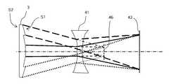
本実施例は、この点に着目したものであり、照明光学素子3の屈折面RSで屈折した光束の径を凹レンズ41で拡大し、径が拡大された光束を視野絞り43に照射する、というものである。 The present embodiment pays attention to this point, and the diameter of the light beam refracted by the refracting surface RS of the illumination
図12に示されるように、照明光学系40a及び顕微鏡40では、凹レンズ41がない状態で照明光学素子3からの複数の光束が重なる面46(被照明面)上に凹レンズ41によって視野絞り43の虚像が形成されるように、凹レンズ41が配置される。これにより、標本面SP、視野絞り43、面46が互いに光学的に共役な位置関係を有する。このため、照明光学素子3のピッチPを視野絞り43の虚像(縮小像)の大きさ程度にすることで、照明の不均一を抑制する機能を低下させることなく、視野絞り43に視野絞り43の径程度の光束径の光を入射させることができる。 As shown in FIG. 12, in the illumination
本実施例によっても、実施例1と同様に、光源1の配光特性に起因する照明の不均一を、従来に比べて少ない光学素子で容易に抑制することができる。また、本実施例によっても、実施例4と同様に、被照明面が拡大又は縮小されて標本面SPに投影されるため、標本面SP上での照明領域の大きさを照明光学素子3の屈折面RSのピッチPとは異なる大きさにすることができる。さらに、本実施例によれば、照明光学素子3のピッチPを視野絞り43の虚像程度の大きさにすればよいので。照明光学素子3の大型化を防止しつつ、上記の効果を得ることができる。 Also in the present embodiment, similarly to the first embodiment, it is possible to easily suppress nonuniform illumination caused by the light distribution characteristics of the
なお、照明光学系40a及び顕微鏡40では、凹レンズ41の設計によって瞳位置を変化する。このため、凹レンズ41によって瞳位置を所望の位置に形成することができるため、FS投影レンズを備えた従来の落射投光管との接続が容易になる。また、凹レンズ41の設計によって標本面SP側のテレセントリック性を変化させることができる。この点も、従来の落射投光管との接続に有利である。 In the illumination
図13は、本実施例に係るプロジェクタ50の構成を例示した図である。プロジェクタ50は、いわゆる液晶プロジェクタであり、照明光を出射する光源1と、コレクタレンズ2と、照明光学素子3と、液晶ディスプレイ(LCD)51と、LCD51を制御する制御部52と、LCD51をスクリーン60に投影する投影レンズ53と、を備える。なお、プロジェクタ50は、スクリーン60を照明する機能を有するという点において、照明装置である。また、本実施例では、コレクタレンズ2、照明光学素子3、LCD51、及び、投影レンズ53が、光源1からの光を標本面SPの領域に面状に照射する照明光学系50aとして機能する。 FIG. 13 is a diagram illustrating a configuration of the
プロジェクタ50では、映像信号を受信した制御部52がその映像信号に従ってLCD51の各画素を制御することで、スクリーン60にLCD51の状態に応じた映像が投影される。 In the
LCDを有する液晶プロジェクタでは、一般に、LCDが均一に照明されることが望ましい。本実施例によれば、LCD51を照明光学素子3で分割された光束が重なる位置に配置することで、光源1の配光特性に起因する照明の不均一を抑制して、LCD51を均一に照明することができる。また、少ない光学素子で照明の不均一を抑制することができるため、照明光学系50a及びプロジェクタ50を小型化することができる。 In a liquid crystal projector having an LCD, it is generally desirable for the LCD to be illuminated uniformly. According to the present embodiment, the
図14は、本実施例に係るプロジェクタ70の構成を例示した図である。プロジェクタ70は、LCD51、制御部52、投影レンズ53の代わりに、ミラー71、デジタルミラーデバイス(DMD、商標)72、制御部73、投影レンズ74を備えている点が、プロジェクタ50とは異なっている。プロジェクタ70は、いわゆるDLPプロジェクタである。なお、プロジェクタ70は、スクリーン60を照明する機能を有するという点において、照明装置である。また、本実施例では、コレクタレンズ2、照明光学素子3、ミラー71、DMD72、及び、投影レンズ74が、光源1からの光を標本面SPの領域に面状に照射する照明光学系70aとして機能する。 FIG. 14 is a diagram illustrating a configuration of the
プロジェクタ70では、映像信号を受信した制御部73がその映像信号に従ってDMD72の各ミラーを制御することで、スクリーン60にDMD72の状態に応じた映像が投影される。 In the
DMDを有するDLPプロジェクタでは、一般に、DMDが均一に照明されることが望ましい。本実施例によれば、DMD72を照明光学素子3で分割された光束が重なる位置に配置することで、光源1の配光特性に起因する照明の不均一を抑制して、DMD72を均一に照明することができる。また、少ない光学素子で照明の不均一を抑制することができるため、照明光学系70a及びプロジェクタ70を小型化することができる。 In a DLP projector having a DMD, it is generally desirable for the DMD to be illuminated uniformly. According to the present embodiment, the
図15は、本実施例に係るステッパー80の構成を例示した図である。ステッパー80は、照明光を出射する光源1と、コレクタレンズ2と、照明光学素子3と、視野絞り81と、コンデンサレンズ82と、ミラー83と、コンデンサレンズ84と、レチクル85と、投影光学系86とを備えている。なお、ステッパー80は、レチクル85を照明し、レチクル85のパターンをウェハWに投影する照明装置である。また、本実施例では、コレクタレンズ2、照明光学素子3、視野絞り81と、コンデンサレンズ82、ミラー83、及び、コンデンサレンズ84が、光源1からの光をレチクル85の領域に面状に照射する照明光学系として機能する。 FIG. 15 is a diagram illustrating the configuration of the
視野絞り81は、レチクル85と光学的に共役な面に配置された可変絞りである。コンデンサレンズ82とコンデンサレンズ84によって、視野絞り81とレチクル85の共役関係が形成されている。視野絞り81の径を可変することで、光源1からの光が照射されるレチクル85上の領域の大きさを変更することができる。投影光学系86は、レチクル85に形成されたパターンをウェハW上に投影する。 The
ステッパー80では、レチクル85が均一に投影されることでレチクル85に形成されたパターンを正しく投影することができる。本実施例によれば、視野絞り81を照明光学素子3で分割された光束が重なる位置に配置することで、光源1の配光特性に起因する照明の不均一を抑制して、レチクル85を均一に照明することができる。また、少ない光学素子で照明の不均一を抑制することができる。 The
図16は、レーザに起因する照明の不均一を抑制する方法について説明するための図である。レーザが出射するレーザ光はガウス分布を有しているため、レーザ光をそのまま照射すると、被照明面は均一に照明されない。このようなレーザに起因する照明の不均一は、図16に示すように、レーザ光の光路中に照明光学素子3を配置することで抑制することができる。 FIG. 16 is a diagram for explaining a method of suppressing illumination non-uniformity caused by a laser. Since the laser beam emitted from the laser has a Gaussian distribution, the surface to be illuminated is not uniformly illuminated when the laser beam is irradiated as it is. Such non-uniform illumination caused by the laser can be suppressed by arranging the illumination
ただし、照明光学素子3から出射したレーザ光は、入射時に比べて大きなNAを有することになる。レーザ光が有するNAをできる限り抑えるためには、照明光学素子3は面P1までの距離ΔLが長くなるように設計された屈折面RSを有することが望ましい。さらに、リレーレンズ90で面P1を拡大して面P2に投影することで、照明領域の大きさを広げることができる。そして、照明範囲の拡大に伴って、レーザ光のNAも更に小さくすることができる。 However, the laser light emitted from the illumination
図17は、本実施例に係るレーザ顕微鏡100の構成を例示した図である。レーザ顕微鏡100は、上述したようなレーザ光で広い範囲を均一に照明する構成を備えたディスクスキャン型のレーザ顕微鏡である。 FIG. 17 is a diagram illustrating the configuration of the
レーザ顕微鏡100は、レーザ101と、面P1を面状に照明する照明光学素子3と、面P1を回転ディスク110のディスク表面111に拡大して投影するリレーレンズ90と、レーザ光を反射させ標本面SPから生じた蛍光を透過させるダイクロイックミラー102と、走査手段である回転ディスク110と、結像レンズ103と、対物レンズ104と、集光レンズ105と、CCD106と、を備えている。また、本実施例では、照明光学素子3、リレーレンズ90、ダイクロイックミラー102、回転ディスク110、結像レンズ103、及び、対物レンズ104が、レーザ101からの光を標本SPの領域に面状に照射する照明光学系として機能する。 The
回転ディスク110は、ピンホールやスリットなどが形成された光を透過する領域(透過領域)を有し、回転により透過領域の位置が変化するように構成された走査手段である。回転ディスク110は、ディスク表面111(面P2)が標本面SP、面P1、及び、CCD106の受光面と光学的に共役な位置関係を有するように、配置されている。 The
レーザ顕微鏡100によれば、ディスク表面111の広い範囲をガウス分布よりも均一な分布を有するレーザ光で面状に照明することができる。このため、回転ディスク110の回転により、標本面SPを均一な強度のレーザ光で走査することができる。また、従来の装置では、ガウス分布に起因する照明の不均一を抑制するために、ガウス分布のピーク近傍のみが照明に利用される。これに対してレーザ顕微鏡100では、レーザ101から出射したレーザ光を無駄なく照明に利用することができる。 According to the
上述した各実施例は、発明の理解を容易にするために具体例を示したものであり、本発明はこれらの実施例に限定されるものではない。照明光学系、照明装置、及び照明光学素子は、特許請求の範囲により規定される本発明の思想を逸脱しない範囲において、さまざまな変形、変更が可能である。この明細書で説明される個別の実施例の文脈におけるいくつかの特徴を組み合わせて単一の実施例としてもよい。 The above-described embodiments are specific examples for facilitating understanding of the invention, and the present invention is not limited to these embodiments. The illumination optical system, illumination device, and illumination optical element can be variously modified and changed without departing from the spirit of the present invention defined by the claims. Several features in the context of the individual embodiments described in this specification may be combined into a single embodiment.
なお、照明光学素子3に入射する光が平行光束である例を示したが、照明光学素子3に入射する光束は、完全な平行光束でなくてもよい。照明光学素子3に入射する光が光軸AXと直交する方向に一定ではない光量を有している場合には、その光を分割して重ね合わせることで分布を平均化する効果が期待できる。 Although an example in which the light incident on the illumination
1 光源
1a 光源像
2 コレクタレンズ
3、6、7、8、21 照明光学素子
4 フライアイレンズ
5、82、84 コンデンサレンズ
9 可変絞り
10、20 照明装置
10a、40a、50a 照明光学系
30、40 顕微鏡
31、43、81 視野絞り
32、44 FS投影レンズ
33、102 ダイクロイックミラー
34、45、104 対物レンズ
41 凹レンズ
42 開口絞り
50、70 プロジェクタ
51 LCD
52、73 制御部
53、74 投影レンズ
60 スクリーン
71、83 ミラー
72 DMD
80 ステッパー
85 レチクル
86 投影光学系
90 リレーレンズ
100 レーザ顕微鏡
101 レーザ
103 結像レンズ
105 集光レンズ
106 CCD
110 回転ディスク
111 ディスク表面
SP 標本面
S1、S2 光学面
AX 光軸
A1、A2、A3 領域
W ウェハ
P1、P2 面
RS、RS2、RS3 屈折面
DESCRIPTION OF
52, 73
80
110
Claims (10)
Translated fromJapanese前記照明光学素子は、前記被照明面に向けられる光学面を有し、
前記光学面は、光軸に直交する直交方向に、それぞれ光を前記所定領域に向けて屈折させる、前記所定領域によって定まる一定のピッチで形成された複数の屈折面を有する
ことを特徴とする照明光学系。An illumination optical system including an illumination optical element that irradiates a predetermined area of a surface to be illuminated with light in a planar shape,
The illumination optical element has an optical surface directed to the illuminated surface,
The optical surface has a plurality of refracting surfaces formed at a constant pitch determined by the predetermined region, each of which refracts light toward the predetermined region in a direction orthogonal to the optical axis. Optical system.
前記複数の屈折面は、前記光軸に沿った断面において、前記光軸となす角度が異なる直線形状を有し、
前記光軸に近い屈折面ほど、前記光軸に沿った断面において、前記光軸と大きな角度をなす
ことを特徴とする照明光学系。The illumination optical system according to claim 1,
The plurality of refracting surfaces have a linear shape with different angles to the optical axis in a cross section along the optical axis,
An illumination optical system characterized in that a refractive surface closer to the optical axis forms a larger angle with the optical axis in a cross section along the optical axis.
前記光学面は、さらに、前記複数の屈折面よりも前記直交方向に前記光軸から離れた位置に、それぞれ光を前記所定領域の一部に向けて屈折させる複数の第2の屈折面を有する
ことを特徴とする照明光学系。The illumination optical system according to claim 1 or 2,
The optical surface further includes a plurality of second refracting surfaces that refract light toward a part of the predetermined region, respectively, at positions farther from the optical axis in the orthogonal direction than the plurality of refracting surfaces. An illumination optical system characterized by that.
前記複数の第2の屈折面は、前記光軸に沿った前記断面において、前記光軸と異なる角度をなす直線形状を有し、
前記光軸に近い第2の屈折面ほど、前記光軸に沿った前記断面において、前記光軸と大きな角度をなす
ことを特徴とする照明光学系。The illumination optical system according to claim 3,
The plurality of second refracting surfaces have a linear shape forming an angle different from the optical axis in the cross section along the optical axis,
An illumination optical system characterized in that the second refractive surface closer to the optical axis forms a larger angle with the optical axis in the cross section along the optical axis.
前記複数の第2の屈折面は、前記直交方向に、前記複数の屈折面が形成されるピッチよりも短い一定のピッチで形成される
ことを特徴とする照明光学系。The illumination optical system according to claim 3 or 4,
The illumination optical system, wherein the plurality of second refracting surfaces are formed in the orthogonal direction at a constant pitch shorter than a pitch at which the plurality of refracting surfaces are formed.
前記照明光学素子は、前記光学面とは反対側に、第2の光学面を有し、
前記第2の光学面は、フレネル面である
ことを特徴とする照明光学系。The illumination optical system according to any one of claims 1 to 5,
The illumination optical element has a second optical surface on the side opposite to the optical surface,
The illumination optical system, wherein the second optical surface is a Fresnel surface.
前記複数の屈折面の各々の前記直交方向の幅は、前記所定領域の前記直交方向の幅に等しい
ことを特徴とする照明光学系。The illumination optical system according to any one of claims 1 to 6,
The width of the plurality of refracting surfaces in the orthogonal direction is equal to the width of the predetermined region in the orthogonal direction.
前記照明光学系に入射する光の光束径を可変する可変絞りを備える
ことを特徴とする照明光学系。The illumination optical system according to any one of claims 3 to 5, further comprising:
An illumination optical system comprising: a variable stop for changing a light beam diameter of light incident on the illumination optical system.
ことを特徴とする照明装置。An illumination device comprising the illumination optical system according to any one of claims 1 to 8.
前記被照明面に向けられる光学面を有し、
前記光学面は、光軸に直交する直交方向に、それぞれ光を前記所定領域に向けて屈折させる前記直交方向に、前記所定領域によって定まる一定のピッチで形成される複数の屈折面を有する
ことを特徴とする照明光学素子。
An illumination optical element that irradiates a predetermined area of a surface to be illuminated with light in a planar shape,
An optical surface directed to the illuminated surface;
The optical surface has a plurality of refractive surfaces formed at a constant pitch determined by the predetermined region in the orthogonal direction that refracts light toward the predetermined region in an orthogonal direction orthogonal to the optical axis. Illuminating optical element characterized.
Priority Applications (3)
| Application Number | Priority Date | Filing Date | Title |
|---|---|---|---|
| JP2014150901AJP6370626B2 (en) | 2014-07-24 | 2014-07-24 | Illumination optical system, illumination device, and illumination optical element |
| US14/801,063US10180234B2 (en) | 2014-07-24 | 2015-07-16 | Illumination optical system, illumination apparatus, and illumination optical element |
| EP15176959.3AEP2977809A1 (en) | 2014-07-24 | 2015-07-16 | Illumination optical element, illumination optical system, and illumination apparatus |
Applications Claiming Priority (1)
| Application Number | Priority Date | Filing Date | Title |
|---|---|---|---|
| JP2014150901AJP6370626B2 (en) | 2014-07-24 | 2014-07-24 | Illumination optical system, illumination device, and illumination optical element |
Publications (2)
| Publication Number | Publication Date |
|---|---|
| JP2016025316Atrue JP2016025316A (en) | 2016-02-08 |
| JP6370626B2 JP6370626B2 (en) | 2018-08-08 |
Family
ID=53716352
Family Applications (1)
| Application Number | Title | Priority Date | Filing Date |
|---|---|---|---|
| JP2014150901AActiveJP6370626B2 (en) | 2014-07-24 | 2014-07-24 | Illumination optical system, illumination device, and illumination optical element |
Country Status (3)
| Country | Link |
|---|---|
| US (1) | US10180234B2 (en) |
| EP (1) | EP2977809A1 (en) |
| JP (1) | JP6370626B2 (en) |
Cited By (3)
| Publication number | Priority date | Publication date | Assignee | Title |
|---|---|---|---|---|
| WO2019069509A1 (en)* | 2017-10-02 | 2019-04-11 | ソニー株式会社 | Fluorescence microscope device and fluorescence microscope system |
| US11487095B2 (en) | 2018-08-09 | 2022-11-01 | Sony Corporation | Optical microscope and system including illumination to change function of biomaterial |
| JP2023069258A (en)* | 2021-11-05 | 2023-05-18 | 株式会社エビデント | Illumination optical system and illumination device |
Families Citing this family (5)
| Publication number | Priority date | Publication date | Assignee | Title |
|---|---|---|---|---|
| US10598935B2 (en)* | 2017-02-14 | 2020-03-24 | Facebook Technologies, Llc | Hybrid lens with a silicone fresnel surface |
| US10705340B2 (en) | 2017-02-14 | 2020-07-07 | Facebook Technologies, Llc | Lens assembly including a silicone fresnel lens |
| KR101799527B1 (en)* | 2017-03-22 | 2017-11-20 | (주)성원티피에스 | Laser source apparatus and lamp system for parking guide including the same |
| CZ2017419A3 (en)* | 2017-07-19 | 2019-01-30 | Varroc Lighting Systems, s.r.o. | Lighting equipment, in particular fog lights, for motor vehicles |
| JP6867916B2 (en)* | 2017-09-05 | 2021-05-12 | オリンパス株式会社 | Observation device |
Citations (6)
| Publication number | Priority date | Publication date | Assignee | Title |
|---|---|---|---|---|
| JPS628101A (en)* | 1985-07-05 | 1987-01-16 | Pioneer Electronic Corp | Fresnel lens |
| JPH01112214A (en)* | 1986-06-13 | 1989-04-28 | Dainippon Screen Mfg Co Ltd | Illuminator for collimated light illumination |
| US5005959A (en)* | 1986-06-13 | 1991-04-09 | Dainippon Screen Mfg. Co., Ltd. | Illumination system |
| DE10331768A1 (en)* | 2003-07-11 | 2005-02-24 | Carl Zeiss Laser Optics Gmbh | Processing workpiece with laser beam comprises dividing laser beam into beam segments, and directing segments with deviating angles onto workpiece so that they overlap on target surface of workpiece |
| US20100150200A1 (en)* | 2008-12-11 | 2010-06-17 | Ho Chih-Chiang | Novel method to optimize micro-optic lens in led flashlight application |
| WO2014037580A1 (en)* | 2012-09-10 | 2014-03-13 | Soitec Solar Gmbh | Concentrator fresnel lens with varying draft angle |
Family Cites Families (28)
| Publication number | Priority date | Publication date | Assignee | Title |
|---|---|---|---|---|
| JPH0658481B2 (en)* | 1985-02-22 | 1994-08-03 | 株式会社ニコン | Multifocal Fresnel lens for camera focus plate |
| DE3750483T2 (en)* | 1986-04-01 | 1995-01-19 | Fuji Photo Film Co Ltd | Optical system for a semiconductor laser beam. |
| US5617163A (en)* | 1993-12-22 | 1997-04-01 | Nikon Corporation | Camera with illuminating optical system |
| ES2129812T3 (en) | 1994-02-16 | 1999-06-16 | Minnesota Mining & Mfg | FRESNEL LENS DOUBLE CROSSED FOR A HIGH PROJECTION. |
| JPH11326605A (en) | 1998-05-12 | 1999-11-26 | Toppan Printing Co Ltd | Condenser lens |
| JP3061779B2 (en)* | 1998-10-12 | 2000-07-10 | 協和電機化学株式会社 | Fresnel lens for enlarged observation of display screen |
| JP2000162705A (en) | 1998-11-25 | 2000-06-16 | Sony Corp | Illuminating device |
| US6594090B2 (en)* | 2001-08-27 | 2003-07-15 | Eastman Kodak Company | Laser projection display system |
| JP2004004169A (en) | 2002-05-30 | 2004-01-08 | Nikon Corp | Microscope illumination device and microscope device |
| US20050041307A1 (en)* | 2003-07-22 | 2005-02-24 | Stephen Barone | Directed Fresnel lenses |
| JP2005043517A (en) | 2003-07-24 | 2005-02-17 | Nikon Corp | Microscope illumination device and microscope equipped with the same |
| JP4579554B2 (en) | 2004-02-12 | 2010-11-10 | オリンパス株式会社 | Microscope illumination system |
| JP5053531B2 (en)* | 2005-09-14 | 2012-10-17 | スリーエム イノベイティブ プロパティズ カンパニー | Fresnel lens |
| DE102006035168A1 (en)* | 2005-11-24 | 2007-06-06 | Taihan-Techren Co. Ltd | Lenses, method and apparatus for focusing solar light for solar photovoltaic generator using the concept of superposition |
| JP5086580B2 (en) | 2006-08-04 | 2012-11-28 | オリンパス株式会社 | Lighting device |
| JP2009069691A (en) | 2007-09-14 | 2009-04-02 | Olympus Corp | Illuminator for microscope |
| US20090250095A1 (en)* | 2008-04-05 | 2009-10-08 | Brent Perry Thorley | Low-profile solar tracking module |
| WO2009125722A1 (en)* | 2008-04-08 | 2009-10-15 | シャープ株式会社 | Optical member for light concentration and concentrator photovoltaic module |
| JP2010134191A (en) | 2008-12-04 | 2010-06-17 | Nikon Corp | Illumination device and microscope device having the same |
| JP5567911B2 (en) | 2009-06-25 | 2014-08-06 | オリンパス株式会社 | Illumination optical system and fluorescence microscope using the same |
| US8358457B2 (en)* | 2009-08-10 | 2013-01-22 | Honeybee Robotics, Ltd. | Miniature rotating transmissive optical drum scanner |
| US9097841B2 (en)* | 2010-03-12 | 2015-08-04 | Luigi Salvatore Fornari | Fresnel lens array with novel lens element profile |
| CN102483565B (en)* | 2010-06-22 | 2014-12-03 | 松下电器产业株式会社 | Laser projector |
| JP5603761B2 (en) | 2010-11-29 | 2014-10-08 | オリンパス株式会社 | Illumination optics for fluorescent microscopes |
| WO2012118108A1 (en)* | 2011-03-01 | 2012-09-07 | パナソニック株式会社 | Collecting lens and multi-segment lens |
| JP5942242B2 (en) | 2011-10-20 | 2016-06-29 | 株式会社目白ゲノッセン | Inspection lighting device |
| IN2014DN06813A (en)* | 2012-02-27 | 2015-05-22 | E Vision Smart Optics Inc | |
| KR102021166B1 (en)* | 2013-09-25 | 2019-09-11 | 다이니폰 인사츠 가부시키가이샤 | Linear fresnel lens sheet, transmissive display device and roll-shaped mold for producing linear fresnel lens sheet |
- 2014
- 2014-07-24JPJP2014150901Apatent/JP6370626B2/enactiveActive
- 2015
- 2015-07-16EPEP15176959.3Apatent/EP2977809A1/ennot_activeWithdrawn
- 2015-07-16USUS14/801,063patent/US10180234B2/enactiveActive
Patent Citations (6)
| Publication number | Priority date | Publication date | Assignee | Title |
|---|---|---|---|---|
| JPS628101A (en)* | 1985-07-05 | 1987-01-16 | Pioneer Electronic Corp | Fresnel lens |
| JPH01112214A (en)* | 1986-06-13 | 1989-04-28 | Dainippon Screen Mfg Co Ltd | Illuminator for collimated light illumination |
| US5005959A (en)* | 1986-06-13 | 1991-04-09 | Dainippon Screen Mfg. Co., Ltd. | Illumination system |
| DE10331768A1 (en)* | 2003-07-11 | 2005-02-24 | Carl Zeiss Laser Optics Gmbh | Processing workpiece with laser beam comprises dividing laser beam into beam segments, and directing segments with deviating angles onto workpiece so that they overlap on target surface of workpiece |
| US20100150200A1 (en)* | 2008-12-11 | 2010-06-17 | Ho Chih-Chiang | Novel method to optimize micro-optic lens in led flashlight application |
| WO2014037580A1 (en)* | 2012-09-10 | 2014-03-13 | Soitec Solar Gmbh | Concentrator fresnel lens with varying draft angle |
Cited By (4)
| Publication number | Priority date | Publication date | Assignee | Title |
|---|---|---|---|---|
| WO2019069509A1 (en)* | 2017-10-02 | 2019-04-11 | ソニー株式会社 | Fluorescence microscope device and fluorescence microscope system |
| US11513330B2 (en) | 2017-10-02 | 2022-11-29 | Sony Corporation | Fluorescence microscope apparatus and fluorescence microscope system |
| US11487095B2 (en) | 2018-08-09 | 2022-11-01 | Sony Corporation | Optical microscope and system including illumination to change function of biomaterial |
| JP2023069258A (en)* | 2021-11-05 | 2023-05-18 | 株式会社エビデント | Illumination optical system and illumination device |
Also Published As
| Publication number | Publication date |
|---|---|
| JP6370626B2 (en) | 2018-08-08 |
| EP2977809A1 (en) | 2016-01-27 |
| US20160025299A1 (en) | 2016-01-28 |
| US10180234B2 (en) | 2019-01-15 |
Similar Documents
| Publication | Publication Date | Title |
|---|---|---|
| JP6370626B2 (en) | Illumination optical system, illumination device, and illumination optical element | |
| US7982950B2 (en) | Measuring system for structures on a substrate for semiconductor manufacture | |
| EP1750154B1 (en) | Microscopic illumination apparatus | |
| US11002534B2 (en) | Patterned light projection apparatus and method | |
| JPWO2017104068A1 (en) | Observation device | |
| JP6090607B2 (en) | Confocal scanner, confocal microscope | |
| JP6895768B2 (en) | Defect inspection equipment and defect inspection method | |
| TW202023069A (en) | Light source apparatus, illumination apparatus, exposure apparatus, and method for manufacturing object | |
| EP3779556B1 (en) | Optical illumination device | |
| WO2017098657A1 (en) | Observation device | |
| WO2013058360A1 (en) | Illumination device for inspections | |
| KR101907845B1 (en) | Transmissive illumination fluorescence microscope comprising Koehler illumination | |
| JP5084183B2 (en) | Epi-illumination optical system for microscope | |
| JP2008040038A (en) | Illuminance equalizing optical element | |
| JP2018101092A (en) | Light field microscope | |
| JP2007033381A (en) | Optical inspection apparatus and its lighting method | |
| TWI611273B (en) | Exposure device | |
| JP7692265B2 (en) | coaxial lighting device | |
| JP5843905B2 (en) | Illumination optical system, exposure apparatus, and device manufacturing method | |
| WO2017068627A1 (en) | Microscope | |
| WO2018011869A1 (en) | Observation device | |
| KR101782672B1 (en) | Prism optical system, illumination optical system, exposure apparatus, and device manufacturing method | |
| JP2021085815A (en) | Light irradiation device, inspection system, and light irradiation method | |
| JP2013190760A (en) | Illuminator for microscope | |
| JP2019056734A (en) | Multipoint confocal microscope |
Legal Events
| Date | Code | Title | Description |
|---|---|---|---|
| A621 | Written request for application examination | Free format text:JAPANESE INTERMEDIATE CODE: A621 Effective date:20170710 | |
| A977 | Report on retrieval | Free format text:JAPANESE INTERMEDIATE CODE: A971007 Effective date:20180409 | |
| A131 | Notification of reasons for refusal | Free format text:JAPANESE INTERMEDIATE CODE: A131 Effective date:20180417 | |
| A521 | Request for written amendment filed | Free format text:JAPANESE INTERMEDIATE CODE: A523 Effective date:20180614 | |
| TRDD | Decision of grant or rejection written | ||
| A01 | Written decision to grant a patent or to grant a registration (utility model) | Free format text:JAPANESE INTERMEDIATE CODE: A01 Effective date:20180703 | |
| A61 | First payment of annual fees (during grant procedure) | Free format text:JAPANESE INTERMEDIATE CODE: A61 Effective date:20180711 | |
| R151 | Written notification of patent or utility model registration | Ref document number:6370626 Country of ref document:JP Free format text:JAPANESE INTERMEDIATE CODE: R151 | |
| R250 | Receipt of annual fees | Free format text:JAPANESE INTERMEDIATE CODE: R250 | |
| R250 | Receipt of annual fees | Free format text:JAPANESE INTERMEDIATE CODE: R250 | |
| S111 | Request for change of ownership or part of ownership | Free format text:JAPANESE INTERMEDIATE CODE: R313111 | |
| R371 | Transfer withdrawn | Free format text:JAPANESE INTERMEDIATE CODE: R371 | |
| S111 | Request for change of ownership or part of ownership | Free format text:JAPANESE INTERMEDIATE CODE: R313111 | |
| R350 | Written notification of registration of transfer | Free format text:JAPANESE INTERMEDIATE CODE: R350 | |
| R250 | Receipt of annual fees | Free format text:JAPANESE INTERMEDIATE CODE: R250 | |
| R250 | Receipt of annual fees | Free format text:JAPANESE INTERMEDIATE CODE: R250 | |
| R250 | Receipt of annual fees | Free format text:JAPANESE INTERMEDIATE CODE: R250 |