JP2016012073A - Display device - Google Patents
Display deviceDownload PDFInfo
- Publication number
- JP2016012073A JP2016012073AJP2014134308AJP2014134308AJP2016012073AJP 2016012073 AJP2016012073 AJP 2016012073AJP 2014134308 AJP2014134308 AJP 2014134308AJP 2014134308 AJP2014134308 AJP 2014134308AJP 2016012073 AJP2016012073 AJP 2016012073A
- Authority
- JP
- Japan
- Prior art keywords
- characteristic
- correction
- curve
- display device
- correction unit
- Prior art date
- Legal status (The legal status is an assumption and is not a legal conclusion. Google has not performed a legal analysis and makes no representation as to the accuracy of the status listed.)
- Pending
Links
Images


Classifications
- G—PHYSICS
- G09—EDUCATION; CRYPTOGRAPHY; DISPLAY; ADVERTISING; SEALS
- G09G—ARRANGEMENTS OR CIRCUITS FOR CONTROL OF INDICATING DEVICES USING STATIC MEANS TO PRESENT VARIABLE INFORMATION
- G09G3/00—Control arrangements or circuits, of interest only in connection with visual indicators other than cathode-ray tubes
- G09G3/20—Control arrangements or circuits, of interest only in connection with visual indicators other than cathode-ray tubes for presentation of an assembly of a number of characters, e.g. a page, by composing the assembly by combination of individual elements arranged in a matrix no fixed position being assigned to or needed to be assigned to the individual characters or partial characters
- G09G3/22—Control arrangements or circuits, of interest only in connection with visual indicators other than cathode-ray tubes for presentation of an assembly of a number of characters, e.g. a page, by composing the assembly by combination of individual elements arranged in a matrix no fixed position being assigned to or needed to be assigned to the individual characters or partial characters using controlled light sources
- G09G3/30—Control arrangements or circuits, of interest only in connection with visual indicators other than cathode-ray tubes for presentation of an assembly of a number of characters, e.g. a page, by composing the assembly by combination of individual elements arranged in a matrix no fixed position being assigned to or needed to be assigned to the individual characters or partial characters using controlled light sources using electroluminescent panels
- G09G3/32—Control arrangements or circuits, of interest only in connection with visual indicators other than cathode-ray tubes for presentation of an assembly of a number of characters, e.g. a page, by composing the assembly by combination of individual elements arranged in a matrix no fixed position being assigned to or needed to be assigned to the individual characters or partial characters using controlled light sources using electroluminescent panels semiconductive, e.g. using light-emitting diodes [LED]
- G09G3/3208—Control arrangements or circuits, of interest only in connection with visual indicators other than cathode-ray tubes for presentation of an assembly of a number of characters, e.g. a page, by composing the assembly by combination of individual elements arranged in a matrix no fixed position being assigned to or needed to be assigned to the individual characters or partial characters using controlled light sources using electroluminescent panels semiconductive, e.g. using light-emitting diodes [LED] organic, e.g. using organic light-emitting diodes [OLED]
- G09G3/3225—Control arrangements or circuits, of interest only in connection with visual indicators other than cathode-ray tubes for presentation of an assembly of a number of characters, e.g. a page, by composing the assembly by combination of individual elements arranged in a matrix no fixed position being assigned to or needed to be assigned to the individual characters or partial characters using controlled light sources using electroluminescent panels semiconductive, e.g. using light-emitting diodes [LED] organic, e.g. using organic light-emitting diodes [OLED] using an active matrix
- G09G3/3233—Control arrangements or circuits, of interest only in connection with visual indicators other than cathode-ray tubes for presentation of an assembly of a number of characters, e.g. a page, by composing the assembly by combination of individual elements arranged in a matrix no fixed position being assigned to or needed to be assigned to the individual characters or partial characters using controlled light sources using electroluminescent panels semiconductive, e.g. using light-emitting diodes [LED] organic, e.g. using organic light-emitting diodes [OLED] using an active matrix with pixel circuitry controlling the current through the light-emitting element
- G—PHYSICS
- G09—EDUCATION; CRYPTOGRAPHY; DISPLAY; ADVERTISING; SEALS
- G09G—ARRANGEMENTS OR CIRCUITS FOR CONTROL OF INDICATING DEVICES USING STATIC MEANS TO PRESENT VARIABLE INFORMATION
- G09G2300/00—Aspects of the constitution of display devices
- G09G2300/08—Active matrix structure, i.e. with use of active elements, inclusive of non-linear two terminal elements, in the pixels together with light emitting or modulating elements
- G09G2300/0809—Several active elements per pixel in active matrix panels
- G09G2300/0842—Several active elements per pixel in active matrix panels forming a memory circuit, e.g. a dynamic memory with one capacitor
- G—PHYSICS
- G09—EDUCATION; CRYPTOGRAPHY; DISPLAY; ADVERTISING; SEALS
- G09G—ARRANGEMENTS OR CIRCUITS FOR CONTROL OF INDICATING DEVICES USING STATIC MEANS TO PRESENT VARIABLE INFORMATION
- G09G2320/00—Control of display operating conditions
- G09G2320/02—Improving the quality of display appearance
- G09G2320/0233—Improving the luminance or brightness uniformity across the screen
- G—PHYSICS
- G09—EDUCATION; CRYPTOGRAPHY; DISPLAY; ADVERTISING; SEALS
- G09G—ARRANGEMENTS OR CIRCUITS FOR CONTROL OF INDICATING DEVICES USING STATIC MEANS TO PRESENT VARIABLE INFORMATION
- G09G2320/00—Control of display operating conditions
- G09G2320/02—Improving the quality of display appearance
- G09G2320/0271—Adjustment of the gradation levels within the range of the gradation scale, e.g. by redistribution or clipping
- G09G2320/0276—Adjustment of the gradation levels within the range of the gradation scale, e.g. by redistribution or clipping for the purpose of adaptation to the characteristics of a display device, i.e. gamma correction
- G—PHYSICS
- G09—EDUCATION; CRYPTOGRAPHY; DISPLAY; ADVERTISING; SEALS
- G09G—ARRANGEMENTS OR CIRCUITS FOR CONTROL OF INDICATING DEVICES USING STATIC MEANS TO PRESENT VARIABLE INFORMATION
- G09G2320/00—Control of display operating conditions
- G09G2320/02—Improving the quality of display appearance
- G09G2320/029—Improving the quality of display appearance by monitoring one or more pixels in the display panel, e.g. by monitoring a fixed reference pixel
- G—PHYSICS
- G09—EDUCATION; CRYPTOGRAPHY; DISPLAY; ADVERTISING; SEALS
- G09G—ARRANGEMENTS OR CIRCUITS FOR CONTROL OF INDICATING DEVICES USING STATIC MEANS TO PRESENT VARIABLE INFORMATION
- G09G2320/00—Control of display operating conditions
- G09G2320/04—Maintaining the quality of display appearance
- G09G2320/043—Preventing or counteracting the effects of ageing
- G09G2320/045—Compensation of drifts in the characteristics of light emitting or modulating elements
- G—PHYSICS
- G09—EDUCATION; CRYPTOGRAPHY; DISPLAY; ADVERTISING; SEALS
- G09G—ARRANGEMENTS OR CIRCUITS FOR CONTROL OF INDICATING DEVICES USING STATIC MEANS TO PRESENT VARIABLE INFORMATION
- G09G2320/00—Control of display operating conditions
- G09G2320/06—Adjustment of display parameters
- G09G2320/0673—Adjustment of display parameters for control of gamma adjustment, e.g. selecting another gamma curve
Landscapes
- Engineering & Computer Science (AREA)
- Physics & Mathematics (AREA)
- Computer Hardware Design (AREA)
- General Physics & Mathematics (AREA)
- Theoretical Computer Science (AREA)
- Control Of Indicators Other Than Cathode Ray Tubes (AREA)
- Electroluminescent Light Sources (AREA)
- Control Of El Displays (AREA)
Abstract
Description
Translated fromJapanese本発明の実施形態は、表示装置に関する。 Embodiments described herein relate generally to a display device.
近年、薄型、軽量、低消費電力の特徴を活かして、液晶表示装置に代表される平面表示装置の需要が急速に伸びている。中でも、オン画素とオフ画素とを電気的に分離し、かつオン画素への映像信号を保持する機能を有する画素スイッチを各画素に設けたアクティブマトリクス型表示装置は、携帯情報機器を始め、種々のディスプレイに利用されている。 In recent years, the demand for flat display devices typified by liquid crystal display devices has been rapidly increased by taking advantage of the features of thinness, light weight, and low power consumption. Among them, an active matrix display device in which each pixel is provided with a pixel switch having a function of electrically separating an on-pixel and an off-pixel and holding a video signal to the on-pixel includes various types of information including portable information devices. It is used for the display.
このような平面型のアクティブマトリクス型表示装置として、自己発光素子を用いた有機EL表示装置が注目され、盛んに研究開発が行われている。有機EL表示装置は、バックライトを必要とせず、高速な応答性から動画再生に適し、さらに低温で輝度低下しないために寒冷地での使用にも適しているという特徴を有している。 As such a flat-type active matrix display device, an organic EL display device using a self-luminous element has attracted attention, and research and development have been actively conducted. The organic EL display device has characteristics that it does not require a backlight, is suitable for moving image reproduction because of high-speed responsiveness, and is suitable for use in a cold region because the luminance does not decrease at low temperatures.
一般に、有機EL表示装置は、複数行、複数列に並んで設けられた複数の画素を備えている。各画素は、自己発光素子である有機EL素子、及び有機EL素子に駆動電流を供給する画素回路により構成され、有機EL素子の発光輝度を制御することにより表示動作を行う。 In general, an organic EL display device includes a plurality of pixels arranged in a plurality of rows and a plurality of columns. Each pixel includes an organic EL element that is a self-light emitting element and a pixel circuit that supplies a drive current to the organic EL element, and performs a display operation by controlling the light emission luminance of the organic EL element.
また、有機EL表示装置では、高画質の画像を再現するため映像信号に各種の補正を行っている。特許文献1には、有機EL表示装置の駆動状態を検出して各種の補正を行う技術が開示されている。 Further, in the organic EL display device, various corrections are performed on the video signal in order to reproduce a high-quality image.
ところで、有機EL表示装置では、入力された映像信号に対して主にEL素子特性とTFT特性の補正を行うパネル特性補正ブロックが設けられている。パネル特性補正では、一般に多点直線近似によるディジタル階調補正が用いられるが、補正ポイント数が少ない場合、滑らかな補正が行われずにスジが視認されることがある。一方、表示品位の低下を防止するために補正ポイント数を増加すると、補正のための回路規模を増大させることになる。 Incidentally, the organic EL display device is provided with a panel characteristic correction block that mainly corrects EL element characteristics and TFT characteristics with respect to an input video signal. In the panel characteristic correction, digital gradation correction by multi-point linear approximation is generally used. However, when the number of correction points is small, streaks may be visually recognized without performing smooth correction. On the other hand, if the number of correction points is increased in order to prevent deterioration in display quality, the circuit scale for correction is increased.
本願発明は斯かる事情に鑑みてなされたものであって、高品位のパネル特性補正を回路規模の増加を抑制して行うことのできる表示装置を提供することを目的とする。 The present invention has been made in view of such circumstances, and an object thereof is to provide a display device capable of performing high-quality panel characteristic correction while suppressing an increase in circuit scale.
一実施形態に係る表示装置は、発光素子と、前記発光素子に発光電流を供給する駆動トランジスタとを含み、基板上にマトリクス状に配置された複数の画素部と、外部から供給される映像信号に前記画素部に供給するための表示用の補正を行うパネル特性補正部と、を有し、前記パネル特性補正部は、前記映像信号を前記発光素子の発光特性の逆特性で変換するEL特性補正部と、前記映像信号を前記駆動トランジスタの駆動特性の逆特性で変換するTFT特性補正部とを備える。 A display device according to an embodiment includes a light emitting element, a driving transistor that supplies a light emitting current to the light emitting element, a plurality of pixel units arranged in a matrix on a substrate, and a video signal supplied from the outside. A panel characteristic correction unit that performs display correction to be supplied to the pixel unit, and the panel characteristic correction unit converts the video signal with an inverse characteristic of the light emission characteristic of the light emitting element. A correction unit; and a TFT characteristic correction unit that converts the video signal with a reverse characteristic of a driving characteristic of the driving transistor.
以下に、本発明の各実施の形態について、図面を参照しつつ説明する。
なお、開示はあくまで一例にすぎず、当業者において、発明の主旨を保っての適宜変更について容易に想到し得るものについては、当然に本発明の範囲に含有されるものである。また、図面は説明をより明確にするため、実際の態様に比べ、各部の幅、厚さ、形状等について模式的に表される場合があるが、あくまで一例であって、本発明の解釈を限定するものではない。また、本明細書と各図において、既出の図に関して前述したものと同様の要素には、同一の符号を付して、詳細な説明を適宜省略することがある。Hereinafter, embodiments of the present invention will be described with reference to the drawings.
It should be noted that the disclosure is merely an example, and those skilled in the art can easily conceive of appropriate modifications while maintaining the gist of the invention are naturally included in the scope of the present invention. In addition, the drawings may be schematically represented with respect to the width, thickness, shape, and the like of each part in comparison with actual aspects for the sake of clarity of explanation, but are merely examples, and the interpretation of the present invention is not limited. It is not limited. In addition, in the present specification and each drawing, elements similar to those described above with reference to the previous drawings are denoted by the same reference numerals, and detailed description may be omitted as appropriate.
図1は、実施形態に係る表示装置を概略的に示す平面図である。図1に示すように、表示装置は、有機ELパネル1およびこの有機ELパネル1の動作を制御するコントローラ2を備えている。
有機ELパネル1は、表示領域3、走査線駆動回路4、及び信号線駆動回路5を有する。FIG. 1 is a plan view schematically showing the display device according to the embodiment. As shown in FIG. 1, the display device includes an
The
表示領域3は、ガラス板等の光透過性を有する絶縁基板上にマトリクス状に配列されたm×n個の表示画素PXを備えている。そして、表示画素PXの配列する行に沿ってゲート線SG(1〜m)が配置され、各表示画素PXに接続されている。また、表示画素PXの配列する列に沿ってn本の信号線SL(1〜n)が配置され、列毎の各表示画素PXに接続されている。更に、高電位電源線Pvddと、低電位電源線Pvssとが各表示画素PXに接続されている。 The
走査線駆動回路4は、ゲート線SG(1〜m)を表示画素PXの行毎に順次駆動する。信号線駆動回路5は、複数の信号線SL(1〜n)を駆動する。走査線駆動回路4、および信号線駆動回路5は、表示領域3の外側で絶縁基板上に一体的に形成され、コントローラ2とともに制御部を構成している。 The scanning
図2は、実施形態の表示装置の画素回路とEL素子との構成を示す図である。ゲート線SG及び信号線SLで囲まれるそれぞれの表示画素PXの領域内に、それぞれRGB各色に発光するEL(Electroluminescence)素子と、それぞれのEL素子を駆動する画素回路とを備えている。なお、図2に示す画素回路は基本的な動作を説明するために簡略化して記載している。 FIG. 2 is a diagram illustrating a configuration of a pixel circuit and an EL element of the display device according to the embodiment. In the region of each display pixel PX surrounded by the gate line SG and the signal line SL, an EL (Electroluminescence) element that emits light of each RGB color and a pixel circuit that drives each EL element are provided. Note that the pixel circuit illustrated in FIG. 2 is illustrated in a simplified manner to explain basic operations.
画素回路は、サンプリングトランジスタSST、駆動トランジスタDRT、及び補助容量Csを備えている。
画素回路において、駆動トランジスタDRTの第1端子は高電位電源線Pvdd(高電位電源)と電気的に接続し、駆動トランジスタDRTの第2端子は補助容量Csを介して駆動トランジスタDRTの制御端子と電気的に接続する。また、駆動トランジスタDRTの第3端子はEL素子のアノード電極と電気的に接続し、EL素子のカソード電極は低電位電源線Pvss(低電位電源)と電気的に接続している。The pixel circuit includes a sampling transistor SST, a drive transistor DRT, and an auxiliary capacitor Cs.
In the pixel circuit, the first terminal of the drive transistor DRT is electrically connected to the high potential power supply line Pvdd (high potential power supply), and the second terminal of the drive transistor DRT is connected to the control terminal of the drive transistor DRT via the auxiliary capacitor Cs. Connect electrically. The third terminal of the drive transistor DRT is electrically connected to the anode electrode of the EL element, and the cathode electrode of the EL element is electrically connected to the low potential power supply line Pvss (low potential power supply).
そして、サンプリングトランジスタSSTの第1端子は信号線SLと電気的に接続し、サンプリングトランジスタSSTの第2端子は駆動トランジスタDRTの制御端子(第3端子)と電気的に接続し、サンプリングトランジスタSSTの制御端子はゲート線SGと電気的に接続している。ここで、ゲート線SGは、有機ELパネル1の左側に配置された走査線駆動回路4によって駆動され、信号線SLは、有機ELパネル1の上部に配置された信号線駆動回路5によって駆動される。 The first terminal of the sampling transistor SST is electrically connected to the signal line SL, the second terminal of the sampling transistor SST is electrically connected to the control terminal (third terminal) of the driving transistor DRT, and the sampling transistor SST The control terminal is electrically connected to the gate line SG. Here, the gate line SG is driven by the scanning
実施形態に係る表示装置において、駆動トランジスタDRT、サンプリングトランジスタSSTは、ここでは同一導電型、例えばNチャネル型のTFT(薄膜トランジスタ)により構成されている。また、駆動トランジスタDRTおよびサンプリングトランジスタSSTをそれぞれ構成する薄膜トランジスタは、全て同一工程、同一層構造で形成され、例えば、半導体層にIGZO、a−Si、あるいはポリシリコンを用いたトップゲート構造の薄膜トランジスタである。なお、サンプリングトランジスタSSTおよび駆動トランジスタDRTは、Nチャネル型に限らず、Pチャネル型としてもよい。駆動トランジスタDRTにPチャネル型を用いる場合は補助容量Csは高電位電源線Pvdd(高電位電源)と制御端子(第3端子)との間に電気的に接続される。 In the display device according to the embodiment, the drive transistor DRT and the sampling transistor SST are configured with the same conductivity type, for example, an N-channel type TFT (thin film transistor). The thin film transistors constituting the drive transistor DRT and the sampling transistor SST are all formed in the same process and in the same layer structure, for example, a top gate thin film transistor using IGZO, a-Si, or polysilicon for the semiconductor layer. is there. Note that the sampling transistor SST and the drive transistor DRT are not limited to the N-channel type, and may be a P-channel type. When the P-channel type is used for the drive transistor DRT, the auxiliary capacitor Cs is electrically connected between the high potential power supply line Pvdd (high potential power supply) and the control terminal (third terminal).
有機ELパネル1の端部に設けられたコントローラ2は、外部の信号源(不図示)から映像信号、同期信号、各種コマンド信号などを通信により取得する。コントローラ2はこれらの信号を受けて走査線駆動回路4への制御信号の生成を行うとともに、信号線駆動回路5を駆動する。信号線駆動回路5は、ディジタル映像信号をD/A変換して信号線SLにアナログの映像信号Vsigを供給する。 The
nライン目のゲート線SG(n)がハイレベル“H”となることで接続されたサンプリングトランジスタSSTが導通し、信号線駆動回路5から出力された映像信号Vsigは補助容量Csに書き込まれる。これによって、駆動トランジスタDRTが導通して電源であるPvdd、Pvss間に電流が流れることでEL素子が発光する。このときに流れる電流の大きさは、補助容量Csの電位、即ち映像信号Vsigに対応する。EL素子の明るさは、EL素子に流れる電流値が大きいほど明るくなり、EL電流は映像信号Vsigによって制御される。従って映像信号Vsigの電圧が高いほどEL電流が増加してEL素子は明るく発光する。 When the n-th gate line SG (n) becomes high level “H”, the connected sampling transistor SST becomes conductive, and the video signal Vsig output from the signal line driving circuit 5 is written in the auxiliary capacitor Cs. Thus, the EL element emits light when the drive transistor DRT is turned on and a current flows between Pvdd and Pvss as power sources. The magnitude of the current flowing at this time corresponds to the potential of the auxiliary capacitor Cs, that is, the video signal Vsig. The brightness of the EL element increases as the current value flowing through the EL element increases, and the EL current is controlled by the video signal Vsig. Therefore, as the voltage of the video signal Vsig is higher, the EL current increases and the EL element emits light brighter.
図3は、実施形態の表示装置のコントローラの構成と信号の接続を示す図である。コントローラ2は、リニアガンマ部21、画像処理部22、EL特性補正部23、TFT特性補正部24、ディザ部25、ドライブ部26、及びタイミングコントローラ27を備えている。 FIG. 3 is a diagram illustrating a configuration of a controller and signal connections of the display device according to the embodiment. The
リニアガンマ部21は、外部信号源から入力された映像信号のガンマ特性をリニアな特性に変換する。画像処理部22は、ホワイトバランス、色温度などのカラーマネージメントに関する処理を映像信号に施す。EL特性補正部23は、EL素子の輝度−電流特性を補正する。TFT特性補正部24は、駆動トランジスタDRTの電圧−電流特性を補正する。ここで、EL特性補正部23とTFT特性補正部24とが上述のパネル特性を構成するパネル特性補正部の主たる要素である。ディザ部25は、擬似的な階調表示を処理する。ドライブ部26は、映像信号を有機ELパネル1(信号線駆動回路5)に対して出力する。タイミングコントローラ27は、外部信号源の同期信号から生成した各種タイミング信号を有機ELパネル1(走査線駆動回路4、信号線駆動回路5など)に対して出力する。 The
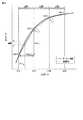
図4は、実施形態の表示装置のパネル特性を例示する図である。 FIG. 4 is a diagram illustrating panel characteristics of the display device according to the embodiment.
図4(a)はEL素子の発光特性、即ちEL素子の輝度−電流特性を示している。EL素子は、流れる電流により発光量が定まるが、図4(a)に示すように輝度−電流特性はリニアではない。また、色(RGB)毎に特性曲線が異なる。従って、EL特性の補正は、赤(R)、緑(G)青(B)の各色毎に独立して行うことが望ましい。 FIG. 4A shows the light emission characteristic of the EL element, that is, the luminance-current characteristic of the EL element. In the EL element, the amount of light emission is determined by the flowing current, but the luminance-current characteristic is not linear as shown in FIG. Further, the characteristic curve is different for each color (RGB). Therefore, it is desirable to correct the EL characteristic independently for each color of red (R), green (G), and blue (B).
図4(b)は駆動トランジスタDRTの駆動特性、即ち駆動トランジスタDRTの電圧−電流特性を示している。トランジスタ特性は非線形なため、図4(b)に示すように電圧−電流特性はリニアではない。但し、赤(R)、緑(G)青(B)の各画素で同じ画素回路を用いれば、上記駆動トランジスタDRTの特性は同じであるため、TFT特性の補正は、RGB共通の特性曲線を用いて行うことができる。 FIG. 4B shows drive characteristics of the drive transistor DRT, that is, voltage-current characteristics of the drive transistor DRT. Since the transistor characteristics are non-linear, the voltage-current characteristics are not linear as shown in FIG. However, if the same pixel circuit is used for each pixel of red (R), green (G) and blue (B), the characteristics of the drive transistor DRT are the same. Can be used.
続いて、従来の多点直線近似によるディジタル階調補正について説明する。 Next, digital gradation correction by conventional multipoint linear approximation will be described.
図5は、従来の多点直線近似による補正方法を示す図である。従来方式は、補正用の特性曲線の内から離散的な複数のポイントを選び、隣接するポイント間(区間)の中間値を直線近似により求めていた。即ち、隣接する2点の座標を(xref1、YREF1)、(xref2、YREF2)としたとき、X座標で(xref1+xadr)の位置におけるY座標の近似値YAPPXを式(1)により求める。
YAPPX = YREF1 + (YREF2 - YREF1) / delta_x * xadr・・・式(1)
delta_x = xref2 - xref1FIG. 5 is a diagram illustrating a conventional correction method using multipoint linear approximation. In the conventional method, a plurality of discrete points are selected from the correction characteristic curve, and an intermediate value between adjacent points (sections) is obtained by linear approximation. That is, when the coordinates of two adjacent points are (xref1, YREF1) and (xref2, YREF2), the approximate value YAPPX of the Y coordinate at the position of (xref1 + xadr) in the X coordinate is obtained by Expression (1).
YAPPX = YREF1 + (YREF2-YREF1) / delta_x * xadr (1)
delta_x = xref2-xref1
図6は、従来の多点直線近似によるグラデーション表示例を示す図である。図6(1)は、ターゲット特性(真の特性)でのグラデーション表示例を示し、図6(2)は、多点直線近似方式でのグラデーション表示例を示している。 FIG. 6 is a diagram showing an example of gradation display by conventional multipoint linear approximation. FIG. 6A shows an example of gradation display with target characteristics (true characteristics), and FIG. 6B shows an example of gradation display with the multipoint linear approximation method.
多点直線近似による補正では、図5に示す区間の境界において近似直線の傾きが不連続に変化する。このため、図6(2)に示すようにグラデーション表示において階調スジが観測されることがある。また、ターゲット特性曲線の曲率が大きい場合、あるいは直線近似の区間の数が少ない場合には、真の値YVALUと近似値YAPPXとの差(誤差)が大きくなる。 In the correction by the multipoint linear approximation, the slope of the approximate line changes discontinuously at the boundary of the section shown in FIG. For this reason, as shown in FIG. 6B, gradation streaks may be observed in gradation display. Further, when the curvature of the target characteristic curve is large, or when the number of linear approximation sections is small, the difference (error) between the true value YVALU and the approximate value YAPPX becomes large.
図7は、実施形態の表示装置のパネル特性補正の構成を説明するための図である。コントローラ2では、最初にEL特性補正部23がEL素子の輝度−電流特性を補正した後、TFT特性補正部24が駆動トランジスタDRTの電圧−電流特性を補正するように2つの特性補正部に分離して構成されている。図7に示すように、変換対象である物理量(輝度、電流、電圧)を明示した場合、コントローラ2で実行される変換の順序と、画素PX内で実行される変換の順序とが対称の関係にある。このように、コントローラ2では、有機ELパネル1内での変換の動作の順序と逆の順番となるようにパネル特性補正回路を構成することによって、EL補正とTFT補正とを互いに分離独立して扱うことが可能となる。 FIG. 7 is a diagram for explaining a configuration of panel characteristic correction of the display device according to the embodiment. In the
なお、EL特性は色毎に異なるため、EL特性補正部23は色毎に異なる特性を補正するように設けられる。一方、TFT特性補正部24の特性は、同じ画素回路を使用している有機ELパネル1内では同じであると見做せるため、TFT特性補正部24は有機ELパネル1内で同一の特性を補正するように設けられる。 Since the EL characteristics are different for each color, the EL
図8は、実施形態の表示装置のTFT特性補正方法を説明するための図である。図8は、図4(b)に示すTFT特性曲線を、基準直線に対して対称となるように変換した補正曲線Aを表している。即ち、図8は、図4(b)に示すTFT特性の逆特性を表す曲線である。これにより入力された信号はTFT特性の逆特性によって変換される。ここで、基準直線は、入力値と出力値とがリニアな関係となるように設けられている。従って、補正曲線Aに従って、入力データ(電流)を出力データ(電圧)に変換することで、駆動トランジスタDRTが流す電流は基準直線に従った値となり、TFTの特性に影響されない値となる。 FIG. 8 is a diagram for explaining a TFT characteristic correction method of the display device according to the embodiment. FIG. 8 shows a correction curve A obtained by converting the TFT characteristic curve shown in FIG. 4B so as to be symmetric with respect to the reference straight line. That is, FIG. 8 is a curve representing the inverse characteristics of the TFT characteristics shown in FIG. As a result, the input signal is converted by the inverse characteristic of the TFT characteristic. Here, the reference straight line is provided so that the input value and the output value have a linear relationship. Therefore, by converting the input data (current) into the output data (voltage) according to the correction curve A, the current flowing through the drive transistor DRT becomes a value according to the reference straight line and becomes a value that is not influenced by the characteristics of the TFT.
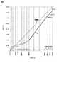
図8に示す方法では、特性曲線Aの形状に応じて区間を可変とする。X座標でXREF0〜XREF16の間は特性曲線Aの傾き又は曲率が大きく、XREF17〜XREF22の間は特性曲線Aの傾き及び曲率は小さい。そのため、区間の間隔をXREF0〜XREF16の間は狭くして、特性曲線Aの曲率の大きい部分については短い間隔で補正することによって誤差の小さい近似値を得ることができる。 In the method shown in FIG. 8, the section is variable according to the shape of the characteristic curve A. In the X coordinate, the slope or curvature of the characteristic curve A is large between XREF0 and XREF16, and the slope and curvature of the characteristic curve A is small between XREF17 and XREF22. Therefore, an approximate value with a small error can be obtained by narrowing the interval between XREF0 to XREF16 and correcting a portion with a large curvature of the characteristic curve A at a short interval.
図9は、実施形態の表示装置のEL特性補正方法を説明するための図である。図9は、図4(a)に示すEL特性曲線を、基準直線に対して対称となるように変換した特性曲線Bを表している。即ち、図9は、図4(a)に示すEL特性の逆特性を表す曲線である。これにより入力された信号はEL特性の逆特性によって変換される。図9では、特性曲線Bの傾き、曲率に応じて5種類の区間幅(XREF0〜XREF6、XREF6〜XREF7、XREF7〜XREF16、XREF16〜XREF19、XREF19〜XREF22)に区分している。 FIG. 9 is a diagram for explaining an EL characteristic correction method for the display device according to the embodiment. FIG. 9 shows a characteristic curve B obtained by converting the EL characteristic curve shown in FIG. 4A so as to be symmetric with respect to the reference straight line. That is, FIG. 9 is a curve showing the inverse characteristic of the EL characteristic shown in FIG. As a result, the input signal is converted by the inverse characteristic of the EL characteristic. In FIG. 9, it is divided into five types of section widths (XREF0 to XREF6, XREF6 to XREF7, XREF7 to XREF16, XREF16 to XREF19, XREF19 to XREF22) according to the slope and curvature of the characteristic curve B.
各区間の幅を任意の値に設定できるようにすると、区間の中間ポイントを算出する時に除算器が必要になり、補正に必要な回路規模の増大と補正処理負荷の増大とが発生することが考えられる。そこで、この回路規模及び処理負荷の増大を、区間幅の設定方法を規定することにより抑制することが可能である。即ち、区間幅は、例えば多点直線近似では式(1)のdelta_xで表される。そこで区間幅を基準値の2n倍(あるいは1/2n倍)(nは1以上の整数)として設定することにより、乗除算をビットシフト演算によって実現することができるため、各区間内の中間ポイントを近似計算するための回路規模の増大と処理負荷の増大とを抑制することができる。If the width of each section can be set to an arbitrary value, a divider is required when calculating the intermediate point of the section, and an increase in circuit scale and correction processing load necessary for correction may occur. Conceivable. Therefore, the increase in the circuit scale and the processing load can be suppressed by defining a section width setting method. That is, the section width is represented by delta_x in the expression (1) in the multipoint linear approximation, for example. Therefore, by setting the section width as 2n times (or 1/2n times) the reference value (n is an integer of 1 or more), multiplication and division can be realized by bit shift operation. It is possible to suppress an increase in circuit scale and an increase in processing load for approximating the intermediate point.
なお、有機ELパネル1に使用するEL素子の材料が変更されたとき、あるいはTFTの設計が変更されたとき、変更された特性曲線の傾き、曲率に応じて自動で区間幅を設定しても良く、手動で区間幅を設定しても良い。 In addition, when the material of the EL element used for the
図10は、実施形態の表示装置の他の特性補正方法を説明するための図である。図10に示す特性補正方法では、新たな曲線近似方式を用いる。 FIG. 10 is a diagram for explaining another characteristic correction method of the display device of the embodiment. In the characteristic correction method shown in FIG. 10, a new curve approximation method is used.
区間1の2つの境界点P1、P2の座標をP1(xref1、YREF1)、P2(xref2、YREF2)とする。次に、境界点P1に対してX座標が同じxref1であり、Y座標がYREF1aである点P1a(xref1、YREF1a)を設ける。そして、入力データ(xref1+xadr1)に対しては、点P1aと点P2とを結ぶ直線を用いて出力データを求める。境界点P1に対してX座標が同じxref1であり、Y座標がYREF1bである点P1b(xref1、YREF1b)を設ける。そして、入力データ(xref1+xadr2)に対しては、点P1bと点P2とを結ぶ直線を用いて出力データを求める。同様にして、入力データの増加に対応した新たな直線を用いて出力データを求める。 The coordinates of the two boundary points P1 and P2 in the
上述の方法は、入力データをX座標軸、出力データをY座標軸として表されるXY座標系で表される補正曲線を近似する補正方法において、X座標軸を複数の区間に分割して補正曲線上に複数の境界点を設定し、隣接する境界点P1、P2間の補正曲線を近似する際、入力データが区間の境界点P1のX座標の値(xref1)からxadrだけ増加するに対応して、境界点P1のY座標の値をxadrの比例係数倍だけ増加させた新たな境界点Qを求め、点P2と点Qとを結ぶ直線を補正曲線として用いて出力データを求める、と表現することができる。 The above-described method is a correction method for approximating a correction curve represented by an XY coordinate system in which input data is represented as an X coordinate axis and output data is represented as a Y coordinate axis, and the X coordinate axis is divided into a plurality of sections and placed on the correction curve. When setting a plurality of boundary points and approximating a correction curve between adjacent boundary points P1 and P2, corresponding to the input data increasing by xadr from the X coordinate value (xref1) of the boundary point P1 of the section, Expressing that a new boundary point Q is obtained by increasing the value of the Y coordinate of the boundary point P1 by a proportional coefficient multiple of xadr, and that output data is obtained using a straight line connecting the point P2 and the point Q as a correction curve. Can do.
この方法は数式を用いると、隣接する2点の座標を(xref1、YREF1)、(xref2、YREF2)としたとき、X座標で(xref1+xadr)の位置におけるY座標の近似値YAPPXを以下の式(2)により求めると表現できる。 In this method, using mathematical formulas, when the coordinates of two adjacent points are (xref1, YREF1) and (xref2, YREF2), the approximate value YAPPX of the Y coordinate at the position of (xref1 + xadr) in the X coordinate is expressed by the following formula ( It can be expressed as calculated by 2).
YAPPX = (YREF1 + xadr * α) + (YREF2 - (YREF1 + xadr * α)) / delta_x * xadr
・・・式(2)
delta_x = xref2 - xref1
αは、xadrの増加に対応する比例係数(0よりも大きい)である。YAPPX = (YREF1 + xadr * α) + (YREF2-(YREF1 + xadr * α)) / delta_x * xadr
... Formula (2)
delta_x = xref2-xref1
α is a proportionality coefficient (greater than 0) corresponding to an increase in xadr.
ここで、式(2)の右辺をxadrについて整理すると式(3)が得られる。
YAPPX = -α * (xadr)2 / delta_x +((YREF2 - YREF1)/ delta_x +α) * xadr + YREF1
・・・式(3)Here, formula (3) is obtained by arranging the right side of formula (2) with respect to xadr.
YAPPX = -α * (xadr)2 / delta_x + ((YREF2-YREF1) / delta_x + α) * xadr + YREF1
... Formula (3)
即ち、近似値YAPPXは、xadrの2次関数として表現されるため、本補正方法は、2次曲線による近似として把握することができる。また、式(3)のxadrの2次の係数は、-α / delta_xである。従って、αが大きいほど(小さいほど)補正曲線の曲率は大きく(小さく)なる。このため、αを選択することによってターゲット補正曲線に近似する精度を調整することができる。 That is, since the approximate value YAPPX is expressed as a quadratic function of xadr, this correction method can be grasped as approximation by a quadratic curve. Further, the quadratic coefficient of xadr in Expression (3) is −α / delta_x. Therefore, the curvature of the correction curve becomes larger (smaller) as α is larger (smaller). For this reason, the precision approximated to the target correction curve can be adjusted by selecting α.
図11は、実施形態の表示装置の他の特性補正方法を説明するための図である。図10に示す曲線は上に凸の形状であった。図11に示す曲線は下に凸の形状である。 FIG. 11 is a diagram for explaining another characteristic correction method of the display device of the embodiment. The curve shown in FIG. 10 has an upwardly convex shape. The curve shown in FIG. 11 has a downwardly convex shape.
区間3の2つの境界点P3、P4の座標をP3(xref3、YREF3)、P4(xref4、YREF4)とする。次に、境界点P3に対してX座標が同じxref3であり、Y座標がYREF3aである点P3a(xref3、YREF3a)を設ける。そして、入力データ(xref3+xadr1)に対しては、点P3aと点P4とを結ぶ直線を用いて出力データを求める。境界点P3に対してX座標が同じxref3であり、Y座標がYREF3bである点P3b(xref3、YREF3b)を設ける。そして、入力データ(xref3+xadr2)に対しては、点P3bと点P4とを結ぶ直線を用いて出力データを求める。同様にして、入力データの増加に対応した新たな直線を用いて出力データを求める。 The coordinates of the two boundary points P3 and P4 in the
上述の方法は、入力データをX座標軸、出力データをY座標軸として表されるXY座標系で表される補正曲線を近似する補正方法において、X座標軸を複数の区間に分割して補正曲線上に複数の境界点を設定し、隣接する境界点P3、P4間の補正曲線を近似する際、入力データが区間の境界点P3のX座標の値(xref3)からxadrだけ増加するに対応して、境界点P3のY座標の値をxadrの比例係数倍だけ減少させた新たな境界点Qを求め、点Qと点P4とを結ぶ直線を補正曲線として用いて出力データを求める、と表現することができる。 The above-described method is a correction method for approximating a correction curve represented by an XY coordinate system in which input data is represented as an X coordinate axis and output data is represented as a Y coordinate axis, and the X coordinate axis is divided into a plurality of sections and placed on the correction curve. When setting a plurality of boundary points and approximating a correction curve between adjacent boundary points P3 and P4, corresponding to the input data increasing by xadr from the X coordinate value (xref3) of the boundary point P3 of the section, Expressing that a new boundary point Q is obtained by reducing the value of the Y coordinate of the boundary point P3 by a proportional coefficient multiple of xadr, and that output data is obtained using a straight line connecting the point Q and the point P4 as a correction curve. Can do.
この方法は数式を用いると、隣接する2点の座標を(xref3、YREF3)、(xref4、YREF4)としたとき、X座標で(xref3+xadr)の位置におけるY座標の近似値YAPPXを以下の式(4)により求めると表現できる。 In this method, using mathematical formulas, when the coordinates of two adjacent points are (xref3, YREF3) and (xref4, YREF4), the approximate value YAPPX of the Y coordinate at the position of (xref3 + xadr) in the X coordinate is expressed by the following formula ( It can be expressed as obtained by 4).
YAPPX = (YREF3 - xadr * α) + (YREF4 - (YREF3 - xadr * α)) / delta_x * xadr
・・・式(4)
delta_x = xref4 - xref3
αは、xadrの増加に対応する比例係数(0よりも大きい)である。YAPPX = (YREF3-xadr * α) + (YREF4-(YREF3-xadr * α)) / delta_x * xadr
... Formula (4)
delta_x = xref4-xref3
α is a proportionality coefficient (greater than 0) corresponding to an increase in xadr.
ここで、式(4)の右辺をxadrについて整理すると式(5)が得られる。
YAPPX = α * (xadr)2 / delta_x +((YREF4 - YREF3)/ delta_x -α) * xadr + YREF3
・・・式(5)
即ち、近似値YAPPXは、xadrの2次関数として表現されるため、本補正方法は、2次曲線による近似として把握することができる。また、式(5)のxadrの2次の係数は、α / delta_xである。従って、αが大きいほど(小さいほど)補正曲線の曲率は大きく(小さく)なる。このため、αを選択することによってターゲット補正曲線に近似する精度を調整することができる。Here, when the right side of the equation (4) is arranged with respect to xadr, the equation (5) is obtained.
YAPPX = α * (xadr)2 / delta_x + ((YREF4-YREF3) / delta_x -α) * xadr + YREF3
... Formula (5)
That is, since the approximate value YAPPX is expressed as a quadratic function of xadr, this correction method can be grasped as approximation by a quadratic curve. Further, the quadratic coefficient of xadr in Expression (5) is α / delta_x. Therefore, the curvature of the correction curve becomes larger (smaller) as α is larger (smaller). For this reason, the precision approximated to the target correction curve can be adjusted by selecting α.
なお、図10、図11に示すαの選択は次の手順によって実行することができる。
(1)ターゲット補正曲線の入力データと出力データとの関係をグラフに作成する。
(2)ターゲット補正曲線の傾き、曲率から複数の区間を設定する。
(3)設定した区間ごとにターゲット補正曲線に近似する多項式を求める。
(4)求めた多項式から各区間毎に曲率を設定する。
ここで、上述の手順はマニュアルで実行しても良く、所定のプログラムを用いて自動で実行しても良く、マニュアルによる処理と自動処理とを適宜組み合わせて実行しても良い。Note that the selection of α shown in FIGS. 10 and 11 can be executed by the following procedure.
(1) Create a graph of the relationship between the input data and output data of the target correction curve.
(2) A plurality of sections are set from the slope and curvature of the target correction curve.
(3) A polynomial that approximates the target correction curve is obtained for each set section.
(4) A curvature is set for each section from the obtained polynomial.
Here, the above-described procedure may be executed manually, may be automatically executed using a predetermined program, or may be executed by appropriately combining manual processing and automatic processing.
しかし、αを任意の値に設定し、またαの種類を増加することで、補正に必要な回路規模の増大と補正処理負荷の増大とが発生することが考えられる。そこで、この回路規模及び処理負荷の増大を、αの値を規定することにより抑制することが可能である。即ち、αを設定する際、基準値の2n倍(あるいは1/2n倍)(nは1以上の整数)として設定することにより、乗除算をビットシフト演算によって実現することができるため、αを演算するための回路規模の増大と処理負荷の増大とを抑制することができる。However, setting α to an arbitrary value and increasing the type of α may increase the circuit scale and the correction processing load necessary for correction. Therefore, the increase in circuit scale and processing load can be suppressed by defining the value of α. That is, when α is set, by setting it as 2n times (or 1/2n times) the reference value (n is an integer of 1 or more), multiplication and division can be realized by bit shift operation. An increase in circuit scale for calculating α and an increase in processing load can be suppressed.
以上、本実施の形態に係る補正方式について説明した。上述のように、本願ではEL補正とTFT補正とを独立して扱うことが可能となっている。そして、図4に示すEL特性とTFT特性とを参照すると、EL特性はTFT特性よりも補正量が少ないことがわかる。従って、有機ELパネル1に求められる特性に応じて、図3に示すコントローラ2でのパネル特性補正機能は次のように複数の態様で構成することができる。 The correction method according to the present embodiment has been described above. As described above, in the present application, EL correction and TFT correction can be handled independently. Then, referring to the EL characteristics and the TFT characteristics shown in FIG. 4, it can be seen that the EL characteristics have a smaller correction amount than the TFT characteristics. Therefore, according to the characteristics required for the
(1)コントローラ2にEL特性補正部23とTFT特性補正部24を設け、共に図10、図11に示す曲線近似補正を実行する。
(2)コントローラ2にEL特性補正部23とTFT特性補正部24を設け、EL特性補正部23は図5に示す直線近似補正を実行し、TFT特性補正部24は図10、図11に示す曲線近似補正を実行する。
(3)コントローラ2にはTFT特性補正部24のみを設け、EL特性補正部23は設けない。TFT特性補正部24は図10、図11に示す曲線近似補正を実行する。(1) The
(2) The
(3) The
なお、上述の実施形態に開示された技術思想は、RGB色に発光するEL素子を用いた表示装置に限られず、白色に発光するEL素子とRGBフィルタとを組み合わせた表示装置についても適用することができる。またEL素子は有機EL素子に限られず、無機EL素子を適用することができる。 The technical idea disclosed in the above embodiment is not limited to a display device using an EL element that emits light of RGB color, but also applies to a display device that combines an EL element that emits white light and an RGB filter. Can do. Further, the EL element is not limited to the organic EL element, and an inorganic EL element can be applied.
本発明の実施の形態として上述した表示装置及び表示装置の駆動方法を基にして、当業者が適宜設計変更して実施し得る全ての表示装置及び表示装置の駆動方法も、本発明の要旨を包含する限り、本発明の範囲に属する。 All display devices and display device driving methods that can be implemented by those skilled in the art based on the above-described display device and display device drive method described above as embodiments of the present invention are also included in the gist of the present invention. As long as it is included, it belongs to the scope of the present invention.
本発明の思想の範疇において、当業者であれば、各種の変更例及び修正例に想到し得るものであり、それら変更例及び修正例についても本発明の範囲に属するものと了解される。例えば、上述の各実施形態に対して、当業者が適宜、構成要素の追加、削除もしくは設計変更を行ったもの、又は、工程の追加、省略若しくは条件変更を行ったものも、本発明の要旨を備えている限り、本発明の範囲に含まれる。 In the scope of the idea of the present invention, those skilled in the art can conceive various changes and modifications, and it is understood that these changes and modifications also belong to the scope of the present invention. For example, those in which the person skilled in the art appropriately added, deleted, or changed the design of the above-described embodiments, or those in which the process was added, omitted, or changed the conditions are also included in the gist of the present invention. As long as it is provided, it is included in the scope of the present invention.
また、本実施形態において述べた態様によりもたらされる他の作用効果について本明細書記載から明らかなもの、又は当業者において適宜想到し得るものについては、当然に本発明によりもたらされるものと解される。 In addition, other functions and effects brought about by the aspects described in the present embodiment, which are apparent from the description of the present specification, or can be appropriately conceived by those skilled in the art, are naturally understood to be brought about by the present invention. .
上記実施形態に開示されている複数の構成要素の適宜な組み合せにより種々の発明を形成できる。例えば、実施形態に示される全構成要素から幾つかの構成要素を削除してもよい。更に、異なる実施形態に亘る構成要素を適宜組み合せてもよい。 Various inventions can be formed by appropriately combining a plurality of constituent elements disclosed in the embodiment. For example, some components may be deleted from all the components shown in the embodiment. Furthermore, you may combine suitably the component covering different embodiment.
PX…画素、SST…サンプリングトランジスタ、DRT…駆動トランジスタ、1…有機ELパネル、2…コントローラ、4…走査線駆動回路、5…信号線駆動回路、21…リニアガンマ部、22…画像処理部、23…EL特性補正部、24…TFT特性補正部。 PX ... pixel, SST ... sampling transistor, DRT ... drive transistor, 1 ... organic EL panel, 2 ... controller, 4 ... scan line drive circuit, 5 ... signal line drive circuit, 21 ... linear gamma unit, 22 ... image processing unit, 23 ... EL characteristic correction unit, 24 ... TFT characteristic correction unit.
Claims (10)
Translated fromJapanese外部から供給される映像信号に前記画素部に供給するための表示用の補正を行うパネル特性補正部と、を有し、
前記パネル特性補正部は、
前記映像信号を前記発光素子の発光特性の逆特性で変換するEL特性補正部と、
前記映像信号を前記駆動トランジスタの駆動特性の逆特性で変換するTFT特性補正部とを備える、表示装置。A plurality of pixel portions including a light emitting element and a driving transistor for supplying a light emitting current to the light emitting element, and arranged in a matrix on the substrate;
A panel characteristic correction unit that performs display correction for supplying to the pixel unit the video signal supplied from the outside,
The panel characteristic correction unit
An EL characteristic correction unit that converts the video signal with a reverse characteristic of the light emission characteristic of the light emitting element;
A display device comprising: a TFT characteristic correction unit that converts the video signal with a reverse characteristic of a driving characteristic of the driving transistor.
前記曲線近似法は、入力データをX座標軸、出力データをY座標軸として表されるXY座標系で表される補正曲線を近似する補正方法であって、
X座標軸を複数の区間に分割して補正曲線上に複数の境界点を設定し、隣接する境界点P1、P2間の補正曲線を近似する際、
入力データが区間の境界点P1のX座標の値(xref1)からxadrだけ増加するのに対応して、当該区間において前記補正曲線が上に凸の場合は境界点P1のY座標の値をxadrの比例係数倍だけ増加させた新たな境界点Qを求め、当該区間において前記補正曲線が下に凸の場合は境界点P1のY座標の値をxadrの比例係数倍だけ減少させた新たな境界点Qを求め、
点P2と点Qとを結ぶ直線を補正曲線として用いて出力データを求める、
請求項2に記載の表示装置。The TFT characteristic correction unit converts the video signal by a curve approximation method using a curve that approximates a correction curve representing the inverse characteristic,
The curve approximation method is a correction method for approximating a correction curve represented by an XY coordinate system represented by using input data as an X coordinate axis and output data as a Y coordinate axis,
When the X coordinate axis is divided into a plurality of sections, a plurality of boundary points are set on the correction curve, and the correction curve between the adjacent boundary points P1 and P2 is approximated,
Corresponding to the input data increasing by xadr from the X coordinate value (xref1) of the boundary point P1 of the section, if the correction curve is convex upward in the section, the value of the Y coordinate of the boundary point P1 is set to xadr. A new boundary point Q increased by a proportional coefficient multiple of x is obtained, and if the correction curve is convex downward in the interval, a new boundary is obtained by reducing the value of the Y coordinate of the boundary point P1 by the proportional coefficient multiple of xadr Find point Q,
Using the straight line connecting the point P2 and the point Q as a correction curve, output data is obtained.
The display device according to claim 2.
前記曲線近似法は、入力データをX座標軸、出力データをY座標軸として表されるXY座標系で表される補正曲線を近似する補正方法であって、
X座標軸を複数の区間に分割して補正曲線上に複数の境界点を設定し、隣接する2点の座標を(xref1、YREF1)、(xref2、YREF2)としたとき、X座標で(xref1+xadr)の位置におけるY座標の近似値YAPPXを以下の式により求める、請求項2に記載の表示装置。
YAPPX = (YREF1 + xadr * α) + (YREF2 - (YREF1 + xadr * α)) / delta_x * xadr
delta_x = xref2 - xref1
αは、xadrの増加に対応する比例係数であり、前記補正曲線が上に凸の場合は0よりも大きい値であり、前記補正曲線が下に凸の場合は0よりも小さい値である。The TFT characteristic correction unit converts the video signal by a curve approximation method using a curve that approximates a correction curve representing the inverse characteristic,
The curve approximation method is a correction method for approximating a correction curve represented by an XY coordinate system represented by using input data as an X coordinate axis and output data as a Y coordinate axis,
When the X coordinate axis is divided into a plurality of sections, a plurality of boundary points are set on the correction curve, and the coordinates of two adjacent points are (xref1, YREF1), (xref2, YREF2), the X coordinate is (xref1 + xadr) The display device according to claim 2, wherein an approximate value YAPPX of the Y coordinate at the position is determined by the following equation.
YAPPX = (YREF1 + xadr * α) + (YREF2-(YREF1 + xadr * α)) / delta_x * xadr
delta_x = xref2-xref1
α is a proportional coefficient corresponding to an increase in xadr, and is a value larger than 0 when the correction curve is convex upward, and a value smaller than 0 when the correction curve is convex downward.
前記直線近似法は、入力データをX座標軸、出力データをY座標軸として表されるXY座標系で表される補正曲線を近似する補正方法であって、
X座標軸を複数の区間に分割して補正曲線上に複数の境界点を設定し、隣接する境界点P1、P2間の補正曲線を近似する際、点P1とP2とを結ぶ直線を補正曲線として用いて出力データを求める、請求項3又は4に記載の表示装置。The EL characteristic correction unit converts the video signal by a linear approximation method using a straight line approximating a correction curve representing the inverse characteristic,
The straight line approximation method is a correction method for approximating a correction curve represented by an XY coordinate system represented by using input data as an X coordinate axis and output data as a Y coordinate axis,
When the X coordinate axis is divided into a plurality of sections, a plurality of boundary points are set on the correction curve, and a correction curve between adjacent boundary points P1 and P2 is approximated, a straight line connecting the points P1 and P2 is used as the correction curve. The display device according to claim 3, wherein output data is obtained using the display device.
前記新たなEL特性補正部は、前記映像信号を変換せずに出力する、請求項1乃至6の内のいずれか1項に記載の表示装置。It has a new EL characteristic correction unit in place of the EL characteristic correction unit,
The display device according to claim 1, wherein the new EL characteristic correction unit outputs the video signal without conversion.
Priority Applications (2)
| Application Number | Priority Date | Filing Date | Title |
|---|---|---|---|
| JP2014134308AJP2016012073A (en) | 2014-06-30 | 2014-06-30 | Display device |
| US14/753,733US9721503B2 (en) | 2014-06-30 | 2015-06-29 | Display device to correct a video signal with inverse EL and drive TFT characteristics |
Applications Claiming Priority (1)
| Application Number | Priority Date | Filing Date | Title |
|---|---|---|---|
| JP2014134308AJP2016012073A (en) | 2014-06-30 | 2014-06-30 | Display device |
Publications (1)
| Publication Number | Publication Date |
|---|---|
| JP2016012073Atrue JP2016012073A (en) | 2016-01-21 |
Family
ID=54931180
Family Applications (1)
| Application Number | Title | Priority Date | Filing Date |
|---|---|---|---|
| JP2014134308APendingJP2016012073A (en) | 2014-06-30 | 2014-06-30 | Display device |
Country Status (2)
| Country | Link |
|---|---|
| US (1) | US9721503B2 (en) |
| JP (1) | JP2016012073A (en) |
Families Citing this family (2)
| Publication number | Priority date | Publication date | Assignee | Title |
|---|---|---|---|---|
| KR20160072344A (en)* | 2014-12-12 | 2016-06-23 | 삼성디스플레이 주식회사 | Organic light emitting display apparatus and driving method thereof |
| JP6817789B2 (en)* | 2016-06-10 | 2021-01-20 | ラピスセミコンダクタ株式会社 | Display driver and semiconductor device |
Citations (5)
| Publication number | Priority date | Publication date | Assignee | Title |
|---|---|---|---|---|
| JPS54118761A (en)* | 1978-03-08 | 1979-09-14 | Chino Works Ltd | Digital linealizer |
| JPH09305139A (en)* | 1996-05-14 | 1997-11-28 | Futaba Corp | Display device |
| JP2001296831A (en)* | 2000-04-13 | 2001-10-26 | Sharp Corp | Image playback method |
| US20080055618A1 (en)* | 2006-08-31 | 2008-03-06 | Evans & Sutherland Computer Corporation | Interpolation table with logarithmically distributed entries |
| JP2013085045A (en)* | 2011-10-06 | 2013-05-09 | Sony Corp | Video display system, video supply device, and display device |
Family Cites Families (10)
| Publication number | Priority date | Publication date | Assignee | Title |
|---|---|---|---|---|
| JP2006115389A (en)* | 2004-10-18 | 2006-04-27 | Eastman Kodak Co | Digital video signal data processing apparatus |
| US20140111567A1 (en)* | 2005-04-12 | 2014-04-24 | Ignis Innovation Inc. | System and method for compensation of non-uniformities in light emitting device displays |
| JP2007183342A (en)* | 2006-01-05 | 2007-07-19 | Nec Electronics Corp | Data converting circuit and display device using the same |
| JP4479709B2 (en)* | 2006-10-27 | 2010-06-09 | セイコーエプソン株式会社 | Image display device, image display method, image display program, recording medium storing image display program, and electronic apparatus |
| TW200912848A (en)* | 2007-04-26 | 2009-03-16 | Sony Corp | Display correction circuit of organic EL panel |
| JP2009180765A (en)* | 2008-01-29 | 2009-08-13 | Casio Comput Co Ltd | Display driving device, display device and driving method thereof |
| US8130182B2 (en)* | 2008-12-18 | 2012-03-06 | Global Oled Technology Llc | Digital-drive electroluminescent display with aging compensation |
| US10319307B2 (en)* | 2009-06-16 | 2019-06-11 | Ignis Innovation Inc. | Display system with compensation techniques and/or shared level resources |
| TWI600000B (en)* | 2013-05-23 | 2017-09-21 | Joled Inc | Image signal processing circuit, image signal processing method and display device |
| KR102128082B1 (en)* | 2013-07-24 | 2020-06-30 | 삼성디스플레이 주식회사 | Organic light emitting display device and driving method thereof |
- 2014
- 2014-06-30JPJP2014134308Apatent/JP2016012073A/enactivePending
- 2015
- 2015-06-29USUS14/753,733patent/US9721503B2/enactiveActive
Patent Citations (5)
| Publication number | Priority date | Publication date | Assignee | Title |
|---|---|---|---|---|
| JPS54118761A (en)* | 1978-03-08 | 1979-09-14 | Chino Works Ltd | Digital linealizer |
| JPH09305139A (en)* | 1996-05-14 | 1997-11-28 | Futaba Corp | Display device |
| JP2001296831A (en)* | 2000-04-13 | 2001-10-26 | Sharp Corp | Image playback method |
| US20080055618A1 (en)* | 2006-08-31 | 2008-03-06 | Evans & Sutherland Computer Corporation | Interpolation table with logarithmically distributed entries |
| JP2013085045A (en)* | 2011-10-06 | 2013-05-09 | Sony Corp | Video display system, video supply device, and display device |
Also Published As
| Publication number | Publication date |
|---|---|
| US9721503B2 (en) | 2017-08-01 |
| US20150379931A1 (en) | 2015-12-31 |
Similar Documents
| Publication | Publication Date | Title |
|---|---|---|
| CN105225631B (en) | Show equipment | |
| KR102091485B1 (en) | Organic light emitting display device and method for driving thereof | |
| US9633604B2 (en) | Display device, method for driving display device, and electronic apparatus | |
| JP5453121B2 (en) | Display device and driving method of display device | |
| US20190103055A1 (en) | Pixel driving circuit and driving method thereof, display panel and display device | |
| TWI633529B (en) | Display, display drive circuit, display drive method, and electronic apparatus | |
| JP6153830B2 (en) | Display device and driving method thereof | |
| US9792858B2 (en) | Display device and method for driving same | |
| JP2009169071A (en) | Display device | |
| JP2009180765A (en) | Display driving device, display device and driving method thereof | |
| CN103778886A (en) | Display apparatus | |
| JP2015125366A (en) | Display device | |
| JP2010145578A (en) | Display device, method of driving display device, and electronic apparatus | |
| WO2015111118A1 (en) | Organic el display apparatus and drive method | |
| JP2010266848A (en) | El display device and driving method thereof | |
| US9747836B2 (en) | Signal processing method, display device, and electronic apparatus | |
| KR20160007883A (en) | Display device | |
| US20150070377A1 (en) | Image signal processing circuit, image signal processing method and display apparatus | |
| US8314758B2 (en) | Display device | |
| JP2016012073A (en) | Display device | |
| JP2009251546A (en) | Display device, method for driving the same, and electronic device | |
| KR102045346B1 (en) | Display panel and organic light emmiting display device inculding the same | |
| JP2005300929A (en) | Display device | |
| KR102478679B1 (en) | Electroluminescent Display Device | |
| JP5319094B2 (en) | Image display device driving method and image display device |
Legal Events
| Date | Code | Title | Description |
|---|---|---|---|
| A621 | Written request for application examination | Free format text:JAPANESE INTERMEDIATE CODE: A621 Effective date:20161212 | |
| A977 | Report on retrieval | Free format text:JAPANESE INTERMEDIATE CODE: A971007 Effective date:20170928 | |
| A131 | Notification of reasons for refusal | Free format text:JAPANESE INTERMEDIATE CODE: A131 Effective date:20171003 | |
| A02 | Decision of refusal | Free format text:JAPANESE INTERMEDIATE CODE: A02 Effective date:20180327 |