JP2015537497A - System and method for detecting wireless charging transmission characteristics - Google Patents
System and method for detecting wireless charging transmission characteristicsDownload PDFInfo
- Publication number
- JP2015537497A JP2015537497AJP2015534564AJP2015534564AJP2015537497AJP 2015537497 AJP2015537497 AJP 2015537497AJP 2015534564 AJP2015534564 AJP 2015534564AJP 2015534564 AJP2015534564 AJP 2015534564AJP 2015537497 AJP2015537497 AJP 2015537497A
- Authority
- JP
- Japan
- Prior art keywords
- voltage
- series element
- transmission
- coil
- current
- Prior art date
- Legal status (The legal status is an assumption and is not a legal conclusion. Google has not performed a legal analysis and makes no representation as to the accuracy of the status listed.)
- Granted
Links
Images


Classifications
- H—ELECTRICITY
- H02—GENERATION; CONVERSION OR DISTRIBUTION OF ELECTRIC POWER
- H02J—CIRCUIT ARRANGEMENTS OR SYSTEMS FOR SUPPLYING OR DISTRIBUTING ELECTRIC POWER; SYSTEMS FOR STORING ELECTRIC ENERGY
- H02J50/00—Circuit arrangements or systems for wireless supply or distribution of electric power
- H02J50/10—Circuit arrangements or systems for wireless supply or distribution of electric power using inductive coupling
- H02J50/12—Circuit arrangements or systems for wireless supply or distribution of electric power using inductive coupling of the resonant type
- H—ELECTRICITY
- H02—GENERATION; CONVERSION OR DISTRIBUTION OF ELECTRIC POWER
- H02J—CIRCUIT ARRANGEMENTS OR SYSTEMS FOR SUPPLYING OR DISTRIBUTING ELECTRIC POWER; SYSTEMS FOR STORING ELECTRIC ENERGY
- H02J50/00—Circuit arrangements or systems for wireless supply or distribution of electric power
- H02J50/40—Circuit arrangements or systems for wireless supply or distribution of electric power using two or more transmitting or receiving devices
- H—ELECTRICITY
- H02—GENERATION; CONVERSION OR DISTRIBUTION OF ELECTRIC POWER
- H02J—CIRCUIT ARRANGEMENTS OR SYSTEMS FOR SUPPLYING OR DISTRIBUTING ELECTRIC POWER; SYSTEMS FOR STORING ELECTRIC ENERGY
- H02J50/00—Circuit arrangements or systems for wireless supply or distribution of electric power
- H02J50/80—Circuit arrangements or systems for wireless supply or distribution of electric power involving the exchange of data, concerning supply or distribution of electric power, between transmitting devices and receiving devices
- H—ELECTRICITY
- H02—GENERATION; CONVERSION OR DISTRIBUTION OF ELECTRIC POWER
- H02J—CIRCUIT ARRANGEMENTS OR SYSTEMS FOR SUPPLYING OR DISTRIBUTING ELECTRIC POWER; SYSTEMS FOR STORING ELECTRIC ENERGY
- H02J50/00—Circuit arrangements or systems for wireless supply or distribution of electric power
- H02J50/90—Circuit arrangements or systems for wireless supply or distribution of electric power involving detection or optimisation of position, e.g. alignment
- H—ELECTRICITY
- H04—ELECTRIC COMMUNICATION TECHNIQUE
- H04B—TRANSMISSION
- H04B5/00—Near-field transmission systems, e.g. inductive or capacitive transmission systems
- H04B5/20—Near-field transmission systems, e.g. inductive or capacitive transmission systems characterised by the transmission technique; characterised by the transmission medium
- H04B5/24—Inductive coupling
- H—ELECTRICITY
- H04—ELECTRIC COMMUNICATION TECHNIQUE
- H04B—TRANSMISSION
- H04B5/00—Near-field transmission systems, e.g. inductive or capacitive transmission systems
- H04B5/70—Near-field transmission systems, e.g. inductive or capacitive transmission systems specially adapted for specific purposes
- H04B5/79—Near-field transmission systems, e.g. inductive or capacitive transmission systems specially adapted for specific purposes for data transfer in combination with power transfer
- H—ELECTRICITY
- H02—GENERATION; CONVERSION OR DISTRIBUTION OF ELECTRIC POWER
- H02J—CIRCUIT ARRANGEMENTS OR SYSTEMS FOR SUPPLYING OR DISTRIBUTING ELECTRIC POWER; SYSTEMS FOR STORING ELECTRIC ENERGY
- H02J50/00—Circuit arrangements or systems for wireless supply or distribution of electric power
- H02J50/60—Circuit arrangements or systems for wireless supply or distribution of electric power responsive to the presence of foreign objects, e.g. detection of living beings
Landscapes
- Engineering & Computer Science (AREA)
- Computer Networks & Wireless Communication (AREA)
- Power Engineering (AREA)
- Signal Processing (AREA)
- Charge And Discharge Circuits For Batteries Or The Like (AREA)
Abstract
Translated fromJapaneseDescription
Translated fromJapanese本開示は、一般に、ワイヤレス電力に関する。より詳細には、本開示は、ワイヤレス電力システムにおける送信特性を検出することを対象とする。 The present disclosure relates generally to wireless power. More particularly, this disclosure is directed to detecting transmission characteristics in a wireless power system.
ますます多くの様々な電子デバイスが、充電式バッテリーを介して電力を供給されるようになっている。そのようなデバイスには、モバイルフォン、携帯型音楽プレーヤ、ラップトップコンピュータ、タブレットコンピュータ、コンピュータ周辺デバイス、通信デバイス(たとえば、ブルートゥースデバイス)、デジタルカメラ、補聴器などが含まれる。バッテリー技術は向上してきたが、バッテリー電源式電子デバイスは、より多くの電力量をますます必要とし、消費するので、頻繁に充電する必要がある。充電式デバイスは、多くの場合に、電源に物理的に接続されるケーブルまたは他の同様のコネクタを通して有線接続によって充電される。ケーブルおよび同様のコネクタは不便な場合があるか、または扱いにくい場合があり、他の欠点を有する場合もある。充電式電子デバイスを充電するか、または電子デバイスに電力を提供するのに用いられることになる電力を自由空間において伝達することができるワイヤレス充電システムは、有線式の充電解決策の欠点の一部を克服する可能性がある。したがって、電子デバイスに電力を効率的および安全に伝達するワイヤレス電力伝達システムおよび方法が望ましい。 An increasing number of different electronic devices are being powered via rechargeable batteries. Such devices include mobile phones, portable music players, laptop computers, tablet computers, computer peripheral devices, communication devices (eg, Bluetooth devices), digital cameras, hearing aids, and the like. While battery technology has improved, battery-powered electronic devices increasingly require and consume more power and therefore require frequent charging. Rechargeable devices are often charged by a wired connection through a cable or other similar connector that is physically connected to a power source. Cables and similar connectors may be inconvenient or cumbersome and may have other drawbacks. Wireless charging systems that can transfer power in free space that will be used to charge or provide power to a rechargeable electronic device are some of the shortcomings of wired charging solutions There is a possibility of overcoming. Accordingly, wireless power transfer systems and methods that efficiently and safely transfer power to electronic devices are desirable.
添付の特許請求の範囲内のシステム、方法、およびデバイスの様々な実装形態の各々は、いくつかの態様を有し、そのどの態様も単独で、本明細書で説明する望ましい属性に関与することはない。添付の特許請求の範囲を限定することなく、本明細書においていくつかの顕著な特徴について説明する。 Each of the various implementations of systems, methods and devices within the scope of the appended claims has a number of aspects, each of which alone is involved in the desired attributes described herein. There is no. Without limiting the scope of the appended claims, some salient features are described herein.
本開示の一態様は、ワイヤレス電力送信デバイスにおける送信特性を検出する方法を提供する。デバイスは、送信コイルに電気的に結合された直列要素を含む。方法は、直列要素の第1の端子における第1の電圧の実数成分および虚数成分を求めるステップを含む。方法は、直列要素の第2の端子における第2の電圧の実数成分および虚数成分を求めるステップをさらに含む。方法は、求められた第1の電圧および第2の電圧に基づいて、直列要素を通る電流の実数成分および虚数成分を求めるステップをさらに含む。方法は、求められた電圧および求められた電流に基づいて、送信特性を求めるステップをさらに含む。方法は、求められた送信特性に基づいて、ワイヤレス電力送信の特性を調整するステップをさらに含む。 One aspect of the present disclosure provides a method for detecting transmission characteristics in a wireless power transmission device. The device includes a series element electrically coupled to the transmit coil. The method includes determining a real component and an imaginary component of the first voltage at the first terminal of the series element. The method further includes determining a real component and an imaginary component of the second voltage at the second terminal of the series element. The method further includes determining a real component and an imaginary component of the current through the series element based on the determined first voltage and second voltage. The method further includes determining a transmission characteristic based on the determined voltage and the determined current. The method further includes adjusting the characteristics of the wireless power transmission based on the determined transmission characteristics.
本開示の別の革新的な態様は、ワイヤレスデバイスを含む。デバイスは、ワイヤレス電力を受信機に送信するように構成された送信コイルを含む。デバイスは、同相(I)クロック信号および直交位相(Q)クロック信号を生成するように構成された直交位相クロック生成器をさらに含む。デバイスは、送信コイルに電気的に結合された直列要素をさらに含む。デバイスは、直列要素の第1の端子における少なくとも1つの信号をI信号およびQ信号のうちの1つで乗算するように構成された第1の混合器をさらに含む。デバイスは、直列要素の第2の端子における少なくとも1つの信号をI信号およびQ信号のうちの1つで乗算するように構成された第2の混合器をさらに含む。 Another innovative aspect of the present disclosure includes a wireless device. The device includes a transmit coil configured to transmit wireless power to the receiver. The device further includes a quadrature clock generator configured to generate an in-phase (I) clock signal and a quadrature (Q) clock signal. The device further includes a series element electrically coupled to the transmit coil. The device further includes a first mixer configured to multiply at least one signal at the first terminal of the series element by one of the I signal and the Q signal. The device further includes a second mixer configured to multiply at least one signal at the second terminal of the series element by one of the I signal and the Q signal.
本開示の別の革新的な態様は、ワイヤレス電力送信デバイスにおける送信特性を検出するための装置を含む。デバイスは、送信コイルに電気的に結合された直列要素を含む。装置は、直列要素の第1の端子における第1の電圧の実数成分および虚数成分を求めるための手段を含む。装置は、直列要素の第2の端子における第2の電圧の実数成分および虚数成分を求めるための手段をさらに含む。装置は、求められた第1の電圧および第2の電圧に基づいて、直列要素を通る電流の実数成分および虚数成分を求めるための手段をさらに含む。装置は、求められた電圧および求められた電流に基づいて、送信特性を求めるための手段をさらに含む。装置は、求められた送信特性に基づいて、ワイヤレス電力送信の特性を調整するための手段をさらに含む。 Another innovative aspect of the present disclosure includes an apparatus for detecting transmission characteristics in a wireless power transmission device. The device includes a series element electrically coupled to the transmit coil. The apparatus includes means for determining a real component and an imaginary component of the first voltage at the first terminal of the series element. The apparatus further includes means for determining a real component and an imaginary component of the second voltage at the second terminal of the series element. The apparatus further includes means for determining a real component and an imaginary component of the current through the series element based on the determined first voltage and second voltage. The apparatus further includes means for determining a transmission characteristic based on the determined voltage and the determined current. The apparatus further includes means for adjusting the characteristics of the wireless power transmission based on the determined transmission characteristics.
本開示の別の革新的な態様は、実行されると、装置に、直列要素の第1の端子における第1の電圧の実数成分および虚数成分を求めさせるコードを含む、非一時的コンピュータ可読媒体を含む。直列要素は、送信コイルに電気的に結合される。媒体は、実行されると、装置に、直列要素の第2の端子における第2の電圧の実数成分および虚数成分を求めさせるコードをさらに含む。媒体は、実行されると、装置に、求められた第1の電圧および第2の電圧に基づいて、直列要素を通る電流の実数成分および虚数成分を求めさせるコードをさらに含む。媒体は、実行されると、装置に、求められた電圧および求められた電流に基づいて、送信特性を求めさせるコードをさらに含む。媒体は、実行されると、装置に、求められた送信特性に基づいて、ワイヤレス電力送信の特性を調整させるコードをさらに含む。 Another innovative aspect of the present disclosure includes a code that, when executed, causes code to determine a real component and an imaginary component of a first voltage at a first terminal of a series element. including. The series element is electrically coupled to the transmit coil. The medium further includes code that, when executed, causes the apparatus to determine the real and imaginary components of the second voltage at the second terminal of the series element. The medium further includes code that, when executed, causes the apparatus to determine a real component and an imaginary component of the current through the series element based on the determined first and second voltages. The medium further includes code that, when executed, causes the device to determine transmission characteristics based on the determined voltage and the determined current. The medium further includes code that, when executed, causes the apparatus to adjust the characteristics of the wireless power transmission based on the determined transmission characteristics.
本明細書で説明する主題の1つまたは複数の実装形態の詳細について、以下の添付の図面および説明において述べる。他の特徴、態様、および利点は、発明の詳細な説明、図面、および特許請求の範囲から明らかになるであろう。以下の図の相対的な寸法が、縮尺通りに描かれていない場合があることに留意されたい。 The details of one or more implementations of the subject matter described in this specification are set forth in the accompanying drawings and the description below. Other features, aspects, and advantages will be apparent from the detailed description of the invention, the drawings, and the claims. Note that the relative dimensions in the following figures may not be drawn to scale.
図面に示された様々な特徴は、縮尺通りに描かれていない場合がある。したがって、明確にするために、様々な特徴の寸法は任意に拡大または縮小されている場合がある。加えて、図面のいくつかは、所与のシステム、方法、またはデバイスの構成要素のすべてを描写していない場合がある。最後に、本明細書および図の全体を通して、同様の特徴を示すために同様の参照番号が使用される場合がある。 Various features shown in the drawings may not be drawn to scale. Accordingly, the dimensions of the various features may be arbitrarily expanded or reduced for clarity. In addition, some of the drawings may not depict all of the components of a given system, method, or device. Finally, like reference numerals may be used throughout the specification and figures to indicate like features.
添付の図面に関する下記の詳細な説明は、本発明の例示的な実施形態の説明として意図されており、本発明が実施され得る唯一の実施形態を表すように意図されていない。本説明全体にわたって使用される「例示的」という用語は、「例、実例、または例示としての役割を果たす」ことを意味しており、必ずしも、他の例示的な実施態様よりも好ましいか、または有利なものと解釈されるべきではない。詳細な説明は、本発明の例示的実施形態の完全な理解をもたらす目的で、具体的な詳細を含んでいる。場合によっては、いくつかのデバイスはブロック図の形で示される。 The following detailed description of the accompanying drawings is intended as a description of exemplary embodiments of the invention and is not intended to represent the only embodiments in which the invention may be practiced. The term "exemplary" as used throughout this description means "serving as an example, instance, or illustration" and is not necessarily preferred over other exemplary embodiments, or It should not be construed as advantageous. The detailed description includes specific details for the purpose of providing a thorough understanding of the exemplary embodiments of the invention. In some cases, some devices are shown in block diagram form.
電力をワイヤレスに伝達することは、物理的な電気導体を使用することなく、電場、磁場、電磁場などに関連する任意の形態のエネルギーを送信機から受信機に伝達することを指し得る(たとえば、電力は、自由空間を通して伝達され得る)。電力伝達を実現するために、ワイヤレス場(たとえば、磁場)内に出力された電力は、「受信コイル」によって受け取られ、捕捉され、または結合され得る。 Transmitting power wirelessly may refer to transmitting any form of energy associated with an electric field, magnetic field, electromagnetic field, etc. from a transmitter to a receiver without using physical electrical conductors (e.g., Power can be transmitted through free space). To achieve power transfer, power output in a wireless field (eg, a magnetic field) can be received, captured, or combined by a “receiver coil”.
図1は、本発明の例示的な実施形態による、例示的なワイヤレス電力伝達システム100の機能ブロック図である。エネルギー伝達を可能にするために、場105を生成するのに、電源(図示せず)から、送信機104に入力電力102を提供することができる。受信機108は、場105に結合し、出力電力110に結合されたデバイス(図示せず)によって蓄積または消費するための出力電力110を生成することができる。送信機104と受信機108の両方は互いに距離112だけ離間される。例示的な一実施形態では、送信機104および受信機108は、相互の共振関係に従って構成される。受信機108の共振周波数および送信機104の共振周波数が、ほぼ同じか、または極めて近いとき、送信機104と受信機108との間の伝送損失は最小となる。したがって、コイルが極めて近い(たとえば、数mm)ことが必要な大型のコイルを必要とする可能性がある純粋に誘導性のソリューションとは対照的に、より長い距離にわたってワイヤレス電力伝達を可能にすることができる。したがって、共振誘導結合技法は、様々な距離にわたっておよび様々な誘導コイル構成を用いて効率の改善および電力伝達を可能にし得る。 FIG. 1 is a functional block diagram of an exemplary wireless
受信機108は、送信機104によって生成されたエネルギー場105内に位置するときに、電力を受信することができる。場105は、送信機104によって出力されたエネルギーが受信機108によって捕捉され得る領域に対応する。場合によっては、場105は、以下でさらに説明するように、送信機104の「近接場」に相当してよい。送信機104は、エネルギー送信を出力するための送信コイル114を含み得る。受信機108は、エネルギー送信からエネルギーを受信または捕捉するための受信コイル118をさらに含む。近接場は、送信コイル114から電力を最小限に放射する送信コイル114内の電流および電荷に起因する強い反応場が存在する領域に相当してよい。場合によっては、近接場は、送信コイル114の約1波長(または波長の数分の一)内にある領域に相当してよい。送信コイル114および受信コイル118は、それらに関連する適用例およびデバイスに応じてサイズを決定される。上述のように、効率的なエネルギー伝達は、電磁波のエネルギーの大部分を非近接場に伝播するのではなく、送信コイル114の場105のエネルギーの大部分を受信コイル118に結合することによって生じさせることができる。場105内に位置するとき、送信コイル114と受信コイル118との間に、「結合モード」を発生させることができる。この結合が起こり得る、送信コイル114および受信コイル118の周りの領域を、本明細書では結合モード領域と呼ぶ。 The
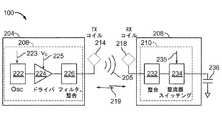
図2は、本発明の様々な例示的な実施形態による、図1のワイヤレス電力伝達システム100に使用され得る例示的な構成要素の機能ブロック図である。送信機204は、発振器222と、ドライバ回路224と、フィルタ/整合回路226とを含むことができる、送信回路206を含んでよい。発振器222は、周波数制御信号223に応答して調整され得る、468.75KHz、6.78MHz、または13.56MHzなどの所望の周波数の信号を生成するように構成され得る。発振器信号は、たとえば送信コイル214の共振周波数で送信コイル214を駆動するように構成されたドライバ回路224に供給され得る。ドライバ回路224は、発振器222から方形波を受け取り、正弦波を出力するように構成されたスイッチング増幅器であってよい。たとえば、ドライバ回路224は、E級増幅器であってよい。また、フィルタ/整合回路226は、高調波または他の不要な周波数をフィルタ処理し、送信機204のインピーダンスを送信コイル214に整合させるために含まれ得る。 FIG. 2 is a functional block diagram of exemplary components that may be used in the wireless
受信機208は、整合回路232と、図2に示すバッテリー236を充電するかまたは受信機208に結合されたデバイス(図示せず)に電力を供給するためにAC電力入力からDC電力出力を生成するための整流器/スイッチング回路234とを含み得る受信回路210を含んでよい。整合回路232は、受信回路210のインピーダンスを受信コイル218に整合させるために含まれ得る。加えて、受信機208および送信機204は、別々の通信チャネル219(たとえば、ブルートゥース、zigbee、セルラーなど)上で通信してよい。代替的には、受信機208および送信機204は、ワイヤレス場205の特性を用いて帯域内シグナリングを介して通信することができる。 The
以下でより十分に説明するように、最初に選択的に無効にすることが可能な関連する負荷(たとえば、バッテリー236)を有する可能性がある受信機208は、送信機204によって送信され受信機208によって受信される電力量がバッテリー236を充電するのに適しているかどうかを判定するように構成され得る。さらに、受信機208は、電力量が適切であると判定すると、負荷(たとえば、バッテリー236)を有効にするように構成され得る。いくつかの実施形態では、受信機208は、バッテリー236を充電することなく、ワイヤレス電力伝達場から受信した電力を直接利用するように構成され得る。たとえば、近接場通信(NFC)または無線周波数識別デバイス(RFID)などの通信デバイスは、ワイヤレス電力伝達場から電力を受け取り、ワイヤレス電力伝達場と相互作用することによって通信し、かつ/または送信機204または他のデバイスと通信するために受信電力を利用するように構成され得る。 As will be described more fully below, a
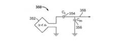
図3は、本発明の例示的な実施形態による、送信コイルまたは受信コイル352を含む、図2の送信回路206または受信回路210の一部分の概略図である。図3に示すように、例示的な実施形態に使用される送信回路または受信回路350は、コイル352を含むことができる。また、コイルは、「ループ」アンテナ352と呼ぶことができるか、または「ループ」アンテナ352として構成することができる。また、コイル352は、本明細書では、「磁気」アンテナまたは誘導コイルと呼ぶことができるか、または「磁気」アンテナまたは誘導コイルとして構成することができる。「コイル」という用語は、別の「コイル」に結合するためのエネルギーをワイヤレスに出力または受信することができる構成要素を指すことが意図される。コイルは、電力をワイヤレスに出力または受信するように構成されるタイプの「アンテナ」と呼ぶこともできる。コイル352は、空芯、またはフェライトコアなどの物理的コア(図示せず)を含むように構成され得る。空芯ループコイルは、コアの近傍に配置された無関係の物理デバイスに対して、より耐用性がある可能性がある。さらに、空芯ループコイル352により、他の構成要素をコア領域内に配置することが可能になる。加えて、空芯ループは、受信コイル218(図2)を送信コイル214(図2)の平面内に配置することをより容易にすることができ、送信コイル214(図2)の結合モード領域は、より強力である可能性がある。 FIG. 3 is a schematic diagram of a portion of the transmit
上述のように、送信機104と受信機108との間のエネルギーの効率的な伝達は、送信機104と受信機108との間に整合した共振またはほぼ整合した共振が生じている間に行われ得る。しかしながら、送信機104と受信機108との間の共振が整合しないときでも、エネルギーを伝達することができるが、効率に影響を及ぼす可能性がある。エネルギーの伝達は、送信コイルの場105からのエネルギーを、近傍にある受信コイルに結合することによって行われ、この場105は、送信コイルからのエネルギーを自由空間に伝播させる代わりに確立される。 As described above, efficient transfer of energy between the
ループコイルまたは磁気コイルの共振周波数は、インダクタンスおよびキャパシタンスに基づいている。インダクタンスは単にコイル352によって生成されたインダクタンスである可能性があるが、キャパシタンスは、所望の共振周波数の共振構造を生成するためにコイルのインダクタンスに加えられ得る。非限定的な例として、共振周波数で信号358を選択する共振回路を生成するために、送信回路または受信回路350にキャパシタ354およびキャパシタ356を加えてよい。したがって、より大きい直径のコイルでは、共振を持続させるのに必要なキャパシタンスのサイズは、ループの直径またはインダクタンスが増加するにつれて減少してよい。さらに、コイルの直径が増加するにつれて、近接場の効率的なエネルギー伝達面積が増加してよい。他の構成要素を使用して形成される他の共振回路も考えられる。別の非限定的な例として、コイル352の2つの端子間に並列にキャパシタを配置してよい。送信コイルに関して、コイル352の共振周波数にほぼ対応する周波数を有する信号358がコイル352への入力であってよい。 The resonant frequency of the loop coil or magnetic coil is based on inductance and capacitance. Although the inductance can simply be the inductance generated by the
一実施形態では、送信機104は、送信コイル114の共振周波数に対応する周波数を有する、時間変動する磁場を出力するように構成され得る。受信機が場105内にあるとき、時間変動する磁場は、受信コイル118内に電流を誘導することができる。上述のように、受信コイル118が送信コイル114の周波数で共振するように構成される場合、エネルギーを効率的に伝達することができる。受信コイル118内に誘導されたAC信号は、負荷を充電するかまたは負荷に電力を供給するために供給され得るDC信号を生成するために上述のように整流され得る。 In one embodiment, the
図4は、本発明の例示的な実施形態による、図1のワイヤレス電力伝達システムに使用され得る送信機404の機能ブロック図である。送信機404は、送信回路406および送信コイル414を含むことができる。送信コイル414は、図3に示すコイル352である可能性がある。送信回路406は、送信コイル414の周りのエネルギー(たとえば、磁束)の生成をもたらす発振信号を提供することにより、送信コイル414にRF電力を提供することができる。送信機404は、任意の適切な周波数で動作してよい。例として、送信機404は、13.56MHzのISM帯域において動作することができる。 FIG. 4 is a functional block diagram of a
送信回路406は、送信回路406のインピーダンス(たとえば、50オーム)を送信コイル414に整合させるための固定インピーダンス整合回路409と、高調波放射を受信機108(図1)に結合されたデバイスの自己ジャミングを防ぐレベルまで低減させるように構成されたローパスフィルタ(LPF)408とを含んでよい。他の例示的な実施形態は、ノッチフィルタを含むが、それに限定されない、異なるフィルタトポロジを含んでよく、ノッチフィルタは、特定の周波数を減衰させる一方で、他の周波数は通過させ、コイル414への出力電力、またはドライバ回路424によって引き出されるDC電流など、測定可能な送電メトリックに基づいて変化し得る、適応インピーダンス整合を含んでよい。送信回路406は、発振器423によって決定されるRF信号を駆動するように構成されたドライバ回路424をさらに含む。送信回路406は、個別のデバイスまたは回路から構成されても、または代わりに、一体型アセンブリから構成されてもよい。送信コイル414から出力される例示的なRF電力は、2.5ワット程度など、1ワット〜10ワット程度であってよい。 The
送信回路406は、隣接するデバイスに取り付けられた受信機を介して隣接するデバイスと対話するための通信プロトコルを実装するように特定の受信機の送信位相(またはデューティサイクル)の間に発振器423を選択的に有効にするための、発振器423の周波数または位相を調整するための、および出力電力レベルを調整するためのコントローラ415をさらに含んでよい。コントローラ415は、本明細書ではプロセッサ415と呼ばれることもあることに留意されたい。発振器位相および送信経路内の関連する回路の調整により、特に、ある周波数から別の周波数に移行する際の帯域外放射の低減が可能になり得る。 The transmit
送信回路406は、送信コイル414によって生成された近接場の近傍における作動中の受信機の有無を検出するための負荷感知回路416をさらに含んでよい。例として、負荷感知回路416は、以下でさらに説明するように、送信コイル414によって生成された場の近傍における作動中の受信機の有無によって影響を及ぼされ得るドライバ回路424に流れる電流を監視する。ドライバ回路424上の負荷に対する変化の検出は、エネルギーを伝送するために発振器423を有効にすべきかどうか、および作動中の受信機と通信すべきかどうかを決定する際に使用するためにコントローラ415によって監視される。以下でより十分に説明するように、ドライバ回路424で測定される電流は、無効なデバイスが送信機404のワイヤレス電力伝達領域内に位置するかどうかを判定するために使用され得る。 The
送信コイル414は、リッツ線とともに、または抵抗損を低く保つために選択された厚さ、幅、および金属のタイプを有するアンテナストリップとして実装され得る。一実装形態では、送信コイル414は、一般に、テーブル、マット、ランプ、または他の携帯性の低い構成などの、より大きい構造と関連付けて構成され得る。したがって、送信コイル414は、一般に、実用的な寸法となるように「巻くこと」を必要としない場合がある。送信コイル414の例示的な実装形態は、「電気的に小型」(すなわち、波長の数分の一)であり、共振周波数を規定するためにキャパシタを使用することにより、より低い使用可能な周波数で共振するように同調され得る。 The transmit
送信機404は、送信機404に関連し得る受信機デバイスの所在および状態に関する情報を収集および追跡してよい。したがって、送信回路406は、(本明細書ではプロセッサとも呼ばれる)コントローラ415に接続される、存在検出器480、密閉型検出器460、またはこれらの組合せを含んでよい。コントローラ415は、存在検出器480および密閉型検出器460からの存在信号に応答してドライバ回路424により送出される電力量を調整してよい。送信機404は、たとえば、建築物中に存在する従来のAC電力を変換するためのAC-DC変換器(図示せず)、従来のDC電源を送信機404に適した電圧に変換するためのDC-DC変換器(図示せず)などの、いくつかの電源を通じて電力を受信することもでき、または従来のDC電源(図示せず)から直接電力を受信することもできる。 The
非限定的な例として、存在検出器480は、送信機404のカバー領域に挿入される、充電されるべきデバイスの最初の存在を感知するために利用される運動検出器であってよい。検出後に、送信機404をオンにすることができ、デバイスによって受信されたRF電力を用いて、所定の方法でRxデバイス上のスイッチを切り替えることができ、それにより、結果として送信機404の駆動点インピーダンスが変化する。 As a non-limiting example,
別の非限定的な例として、存在検出器480は、たとえば、赤外線検出手段、運動検出手段、または他の適切な手段によって人を検出することが可能な検出器であってよい。いくつかの例示的な実施形態では、送信コイル414が特定の周波数で送信することができる電力量を制限する規定が存在してよい。場合によっては、これらの規定は、人を電磁放射から守ることを意図されている。しかしながら、送信コイル414が、たとえば、ガレージ、工場の現場、店舗などの、人によって占有されないか、または人によって占有される頻度が低い領域に位置する環境が存在し得る。これらの環境に人間がいない場合は、通常の電力制限規定を超えて送信コイル414の電力出力を増加させることを許容し得る。言い換えれば、コントローラ415は、人の存在に応答して、送信コイル414の電力出力を、規制レベルまたはそれ未満に調整し、かつ人が送信コイル414の電磁場から規制距離の外側にいる場合は、送信コイル414の電力出力を、規制レベルを超えるレベルに調整してよい。 As another non-limiting example,
非限定的な例として、密閉型検出器460(本明細書では、密閉型コンパートメント検出器または密閉型空間検出器と呼ばれることもある)は、包囲体が閉状態または開状態であることを判定するための感知スイッチなどのデバイスであってよい。送信機が閉状態の包囲体内にあるとき、送信機の電力レベルを増加させてよい。 As a non-limiting example, a sealed detector 460 (sometimes referred to herein as a sealed compartment detector or a sealed spatial detector) determines that the enclosure is closed or open. It may be a device such as a sensing switch for When the transmitter is in a closed enclosure, the transmitter power level may be increased.
例示的な実施形態では、送信機404がいつまでもオンのままではない方法を使用してよい。この場合、送信機404は、ユーザが決定した時間後に切断するようにプログラムされ得る。この特徴は、送信機404の周囲のワイヤレスデバイスが十分充電された後、送信機404、特にドライバ回路424が長く動作するのを防ぐ。このイベントは、リピータまたは受信コイルより送信された、デバイスが十分充電されたという信号を検出するための回路の故障によるものである可能性がある。その周囲に別のデバイスが配置されている場合に、送信機404が自動的にシャットオフすることを防止するために、送信機404の自動シャットオフ機能は、その周囲で動作が検出されずに、定められた期間が経過した後にだけ、アクティブ化されてよい。ユーザが、望み通りに、無活動時間間隔を決定し、それを変更できてよい。非限定的な例として、この時間間隔は、特定のタイプのワイヤレスデバイスが最初に完全に放電したという仮定の下に、そのデバイスを完全に充電するのに必要な時間間隔よりも長くてよい。 In an exemplary embodiment, a method may be used in which
上記で説明したように、負荷感知回路416は、ドライバ回路424に流れる電流を監視することができる。一実施形態では、ドライバ回路424で検出された電流を使用して、意図しない負荷に対して失われた電力を相殺することができる。意図しない負荷としては、たとえば、システムの動作をヒートアップさせるまたは劣化させる可能性がある導電性のループまたは表面を挙げることができる。一実施形態では、コントローラ415は、ドライバ回路424によって消費されるDC電力を、たとえば、受信機208(図2)などの登録された負荷によって報告される負荷電力と比較することができる。しかしながら、いくつかの実施形態では、DC-RF変換効率は負荷条件に応じて異なり得る。したがって、ドライバ回路424で測定された電流は、送信された電力を正確に反映しない場合がある。いくつかの実施形態では、送信回路406は、順方向電力および反射電力を測定するように構成された方向性結合器を含むことができる。しかしながら、いくつかの実施形態では、方向性結合器は送信回路の効率を低下させるおよび/または高い実装コストをもたらす可能性がある。 As described above, the
一実施形態では、送信回路406は、送信コイル414に結合された電力検出器490を含むことができる。電力検出器490は、送信電力を示す1つまたは複数の特性を測定するように構成され得る。一実施形態では、電力検出器490は送信コイル414に容量結合され得る。たとえば、電力検出器490は、容量性電圧分割器を介して差動電圧を測定するように構成され得る。一実施形態では、電力検出器490は抵抗性電圧分割器を実装することができる。電力検出器490は、整合回路409と送信コイル414との間の電圧および/または電流を測定することができる。電力検出器490は、電圧および/または電流をベクトル的におよび/または差動的に測定することができる。コントローラ415は、測定された送信電力を電力検出器490から受信することができ、測定された送信電力を、受信機208(図2)などの受信機によって報告される受信された送信電力と比較することができる。 In one embodiment, the transmit
図5は、本発明の例示的な実施形態による、図1のワイヤレス電力伝達システムに使用され得る受信機508の機能ブロック図である。受信機508は、受信コイル518を含み得る受信回路510を含む。受信機508は、それに受信電力を提供するためのデバイス550にさらに結合する。受信機508は、デバイス550の外部にあるものとして示されているが、デバイス550に統合されてよいことに留意されたい。エネルギーは、受信コイル518にワイヤレスに伝播され、次いで受信回路510の残りの部分を介してデバイス550に結合され得る。例として、充電デバイスには、モバイルフォン、携帯型音楽プレーヤ、ラップトップコンピュータ、タブレットコンピュータ、コンピュータ周辺デバイス、通信デバイス(たとえば、ブルートゥースデバイス)、デジタルカメラ、補聴器(および他の医療用デバイス)などのデバイスが含まれ得る。 FIG. 5 is a functional block diagram of a
受信コイル518は、送信コイル414(図4)と同じ周波数で、または特定の周波数範囲内で共振するように同調され得る。受信コイル518は、送信コイル414と同様の寸法を有しても、または関連するデバイス550の寸法に基づいて異なるサイズを有してもよい。例として、デバイス550は、送信コイル414の直径または長さよりも小さい直径寸法または長さ寸法を有するポータブル電子デバイスであってよい。そのような例では、受信コイル518は、同調キャパシタ(図示せず)のキャパシタンス値を低減させ、受信コイルのインピーダンスを増加させるために多巻きコイルとして実装され得る。例として、受信コイル518は、コイルの直径を最大化し、受信コイル518のループ巻き数(すなわち、巻回)および巻線間キャパシタンスを低減するために、デバイス550の実質的な外周の周りに配置されてよい。 The receive
受信回路510は、受信コイル518に対するインピーダンス整合を可能にしてよい。受信回路510は、受信されたRFエネルギー源をデバイス550によって使用するための充電電力に変換するための電力変換回路506を含む。電力変換回路506は、RF-DC変換器520を含み、DC-DC変換器522を含んでもよい。RF-DC変換器520は、受信コイル518で受信されたRFエネルギー信号を、Vrectで表される出力電圧を有する非交流電力に整流する。DC-DC変換器522(または他の電力調整器)は、整流されたRFエネルギー信号を、VoutおよびIoutによって表される出力電圧および出力電流を有する、デバイス550に適合するエネルギーポテンシャル(たとえば、電圧)に変換する。部分的および完全な整流器、調整器、ブリッジ、ダブラー、ならびにリニア変換器およびスイッチング変換器を含む、種々のRF-DC変換器が企図される。The receiving
受信回路510は、受信コイル518を電力変換回路506に接続するための、あるいは電力変換回路506を切断するための、スイッチング回路512をさらに含んでよい。電力変換回路506から受信コイル518を切断することにより、デバイス550の充電を中断するだけでなく、送信機404(図2)から「見た」「負荷」も変化する。 The
上記で開示したように、送信機404は、送信機ドライバ回路424に供給されるバイアス電流の変動を検出することができる負荷感知回路416を含む。したがって、送信機404は、受信機が送信機の近接場内に存在することを判定するための機構を有する。 As disclosed above, the
複数の受信機508が送信機の近接場内に存在するとき、他の受信機をより効率的に送信機に結合させるために、1つまたは複数の受信機の装荷および除荷を時間多重化することが望ましい場合がある。受信機508はまた、他の近くの受信機への結合を解消するか、または近くの送信機への装荷を低減させるためにクローキングされ得る。受信機のこの「除荷」は、本明細書では「クローキング」としても知られる。さらに、受信機508によって制御され送信機404によって検出される、除荷と装荷との間のこのスイッチングは、以下でより十分に説明するように、受信機508から送信機404への通信機構を実現することができる。加えて、受信機508から送信機404にメッセージを送信することを可能にするプロトコルが、このスイッチングに関連付けられ得る。例として、スイッチング速度は、100μ秒程度であってよい。 When
例示的な一実施形態では、送信機404と受信機508との間の通信は、従来の双方向通信(すなわち、結合場を使用する帯域内シグナリング)ではなく、デバイス感知および充電制御機構を指す。言い換えれば、送信機404は、エネルギーが近接場で利用可能であるかどうかを調整するために送信信号のオン/オフキーイングを使用してよい。受信機は、これらのエネルギー変化を送信機404からのメッセージとして解釈してよい。受信機側から、受信機508は、どれくらいの電力が場から受け入れられているかを調整するために受信コイル518の同調および非同調を使用してよい。場合によっては、同調および非同調は、スイッチング回路512を介して実現され得る。送信機404は、場からの使用される電力のこの差を検出し、これらの変化を受信機508からのメッセージとして解釈してよい。送信電力の変調および負荷挙動の他の形態を利用してよいことに留意されたい。 In an exemplary embodiment, communication between
受信回路510は、送信機から受信機への情報信号伝達に対応し得る、受信エネルギーの変動を識別するために使用される、信号伝達検出器/ビーコン回路514をさらに含んでよい。さらに、シグナリングおよびビーコン回路514を用いて、低減されたRF信号エネルギー(すなわち、ビーコン信号)の送信を検出することもでき、ワイヤレス充電用の受信回路510を構成するために、その低減されたRF信号エネルギーを整流して、受信回路510内の電力を供給されていない回路または電力を使い果たした回路のいずれかを呼び起こすための公称電力を生成することもできる。 The receiving
受信回路510は、本明細書で説明するスイッチング回路512の制御を含む、本明細書において説明される受信機508のプロセスを協調させるためのプロセッサ516をさらに含む。また、受信機508のクローキングは、充電電力をデバイス550に提供する外部の有線充電ソース(たとえば、壁コンセント/USB電力)の検出を含む他のイベントが発生したときにも行われる可能性がある。プロセッサ516は、受信機のクローキングを制御するのに加えて、ビーコン回路514を監視してビーコン状態を判定し、送信機404から送信されたメッセージを抽出してもよい。プロセッサ516は、性能の改善のためにDC-DC変換器522を調整してもよい。 The
上記で説明したように、受信機508は、受信された電力を測定し、受信された電力を、たとえば、別個の通信チャネル219(図2)を介して送信機404(図4)に報告するように構成され得る。いくつかの実施形態では、プロセッサ516は、受信された電力を求め、求められた電力を送信機404に送信するように構成される。いくつかの実施形態では、充電デバイス550は電力検出器を含むことができ、充電デバイス550は求められた電力を送信機404に送信するように構成され得る。 As described above, the
図6は、図4の送信回路406に使用され得る送信回路600の一部分の概略図である。送信回路600は、上記に図4において説明したように、ドライバ回路624を含んでよい。上述のように、ドライバ回路624は、方形波を受け取り、送信回路650に供給する正弦波を出力するように構成され得るスイッチング増幅器であってよい。場合によっては、ドライバ回路624は、増幅器回路と呼ばれることがある。ドライバ回路624は、E級増幅器として示されているが、本発明の実施形態によって任意の適切なドライバ回路624が使用されてよい。ドライバ回路624は、図4に示されるように、発振器423からの入力信号602によって駆動することができる。また、ドライバ回路624は、送信回路650を介して送出され得る最大電力を制御するように構成された駆動電圧VDを提供され得る。高調波を解消または低減するために、送信回路600は、フィルタ回路626を含むことができる。フィルタ回路626は、3極(キャパシタ634、インダクタ632、およびキャパシタ636)ローパスフィルタ回路626であってよい。FIG. 6 is a schematic diagram of a portion of a transmit
フィルタ回路626によって出力された信号は、コイル614を備える送信回路650に与えることができる。送信回路650は、ドライバ回路624によって供給されるフィルタ処理済み信号の周波数で共振する可能性がある、(たとえば、コイルのインダクタンスもしくはキャパシタンス、または追加のキャパシタ構成要素に起因する可能性がある)あるキャパシタンス620およびインダクタンスを有する直列共振回路を含んでよい。送信回路650の負荷は、可変抵抗器622によって表すことができる。この負荷は、送信回路650から電力を受け取るように置かれたワイヤレス電力受信機508の関数であってよい。 The signal output by the
様々な実施形態では、図1〜図6を参照して上述したワイヤレス電力送信システム100は、近くのオブジェクトの検出に基づいて、ワイヤレス電力送信を変更することができる。近くのオブジェクトは、指定受信機、充電されるべきデバイス、および/または外部オブジェクトを含み得る。外部オブジェクトは、指定送信目標以外の何か(すなわち、非充電デバイス)、たとえば、寄生受信機(parasitic receiver)、無生物オブジェクト、または生物(たとえば、人間、動物など)などであってよい。寄生受信機は、たとえば、非電子金属製オブジェクト、無許可充電可能デバイスなどを含み得る。 In various embodiments, the wireless
たとえば、図4を参照して上述したように、送信機404は、存在検出器480を含むことができ、検出器480は、近くのオブジェクトの存在、距離、配向、および/または場所を検出することができる。他の様々な実施形態では、存在検出器480は、別の場所、たとえば、受信機508上、または他の所などに配置されてよい。コントローラ415は、外部オブジェクトが第1の距離以内で検出されたとき、送信電力を削減してよい。様々な実施形態では、ワイヤレス電力送信システム100は、生物学的安全性、防火性などに関する規則または規定に従って、ワイヤレス電力送信の特性を調整することができる。たとえば、ワイヤレス電力送信システム100は、近くの人体までの距離が与えられると、人体に届く電磁場が閾値を下回るように、送信電力を調整することができる。 For example, as described above with reference to FIG. 4, the
様々な実施形態では、存在検出器480は、見通し線検出機構に基づいて、近くのオブジェクトの存在を検出することができる。見通し線検出機構は、たとえば、赤外線検出、超音波検出、レーザー検出などを含み得る。テーブルや机などの不透過表面を通して電力が送信され得る、組込み送信機を含む実施形態では、非見通し線検出機構を使うことが好ましい場合がある。非見通し線機構は、たとえば、容量検出、放射検出などを含み得る。本明細書で説明する様々な実施形態では、存在検出器480は、高調波検出システムを使用して、基本システム周波数の高調波における受信信号強度の変化に基づいて、近くの物体の存在、距離、配向、および/または位置を検出することができる。 In various embodiments,
図2に戻って参照すると、いくつかの実施形態では、ワイヤレス電力伝達システム100は、複数の受信機208を含むことができる。一実施形態では、TXコイル214のサイズは固定である。したがって、送信機204は異なるサイズのRXコイル218にうまく整合しない場合がある。様々な理由で、送信機204が複数のTXコイル214を使用することが望ましい場合がある。いくつかの実施形態では、複数のTXコイル214をアレイに配列することができる。いくつかの実施形態では、アレイはモジュール式であってもよい。いくつかの実施形態では、アレイは同じサイズまたは実質的に同じサイズのTXコイル214を含むことができる。 Referring back to FIG. 2, in some embodiments, the wireless
様々な実施形態では、受信機208の位置および/またはそのRXコイル218のサイズに基づいて、各TXコイル214を別個にアクティブにすることができる。たとえば、単一のTXコイル214は、ワイヤレス電力を比較的小さいRXコイル218を有する近くの受信機208に与えることができる。一方、複数のTXコイル214は、ワイヤレス電力を比較的大きいRXコイル218を有する近くの受信機に与えることができる。RXコイル218の近くではないTXコイル214を非アクティブにすることができる。 In various embodiments, each
いくつかの実施形態では、複数のTXコイル214は大きい送信エリアを形成することができる。送信エリアはスケーラブルで、追加のTXコイル214を使用してより大きいエリアをカバーするものであってもよい。TXコイル214は、大きいエリアにわたるデバイスの自由な配置を可能にすることができる。さらに、TXコイル214は、複数の受信機208を同時に充電するように構成され得る。いくつかの実施形態では、個別のTXコイル214は互いに結合することができる。したがって、ワイヤレス電力伝達システム100がTXコイル214を減結合するための方法、システム、および/または装置を含むことが望ましい場合がある。 In some embodiments, multiple TX coils 214 can form a large transmission area. The transmission area may be scalable and use an
図7は、本発明の例示的な実施形態による、図1のワイヤレス電力伝達システムに使用され得る送信回路700の一部分の機能ブロック図である。様々な実施形態では、図7に提示された要素を平衡方式またはシングルエンド方式で構成することができ、図7およびさらなる説明はこの例を平衡方式で提示している。送信回路700は、直交位相クロック生成器710と、送信増幅器720と、送信フィルタおよび/または整合回路730と、正測定キャパシタCMPおよび負測定キャパシタCMNと、正直列キャパシタCSPおよび負直列キャパシタCSNと、送信コイルLTXと、差動混合器740aおよび740bと、加算増幅器750aおよび750bと、ローパスフィルタ(LPF)760aおよび760bと、アナログデジタル変換器(ADC)770aおよび770bと、プロセッサ780とを含むことができる。FIG. 7 is a functional block diagram of a portion of a transmit
様々な実施形態では、送信回路700は、送信電力またはコイルインピーダンスなどの、送信コイルLTXにおける送信特性を求めるように構成され得る。たとえば、送信回路700は、送信コイルLTXに印加されたRF電圧および/または電流を測定するように構成され得る。送信回路700は、ベクトル測定を行うように構成され得る。たとえば、送信回路700は、送信コイルLTXに印加された電流および/または電圧の振幅と位相の両方を測定することができる。一実施形態では、送信回路700は、電力検出器490(図4)を実装するまたは含むことができる。In various embodiments, the
直交位相クロック生成器710は、同相(I)クロック信号および直交位相(Q)クロック信号(正または負のいずれか)を送信増幅器720ならびに混合器740aおよび740bに与えるように働く。図示の実施形態では、直交位相クロック生成器710は、発振器入力およびプロセッサ780による制御に基づいてI/Q信号を生成するように構成される。一実施形態では、発振器入力は送信周波数の4倍であり得る。たとえば、約468.75KHz、6.78MHz、および13.56MHzの送信周波数を有する様々な実施形態では、発振器入力はそれぞれ、約1.87MHz、27.12MHz、および54.24MHzであり得る。一実施形態では、発振器入力は発振器423(図4)から受信され得る。 The
直交位相クロック生成器710は、発振器入力周波数の4分の1(たとえば、6.78MHz)で4つのクロック信号I、Q、I'、およびQ'(総称して「I/Q」と呼ばれる)を生成するように構成され得る。クロックI、Q、I'、およびQ'の各々は異なる位相(たとえば、0度、90度、180度、および270度)を表すことができる。したがって、IはQの前に90度進むことができる。I'およびQ'はそのそれぞれの出力IおよびQの反転バージョンとすることができ、メイン信号IおよびQの180位相シフトを与えることができる。他の位相ステップが使用され得る(たとえば、45度、60度など)ことを当業者は諒解されよう。 The
直交位相クロック生成器710は、正弦信号と余弦信号の両方を混合器740aおよび740bに選択的に与えることができる。様々な実施形態では、正弦信号および余弦信号は、(たとえば、アナログ増幅器を含む実施形態では)正弦波信号および(たとえば、デジタル増幅器を含む実施形態では)方形波を含むことができる。たとえば、直交位相クロック生成器710は、1つまたは複数のマルチプレクサを介してクロック信号I、Q、I'、およびQ'のうちの1つまたは複数を混合器740aおよび740bに選択的に与えることができる。たとえば、直交位相クロック生成器710は、混合器740aおよび740bごとに1つのマルチプレクサを含むことができる。一実施形態では、選択されたクロック信号I/Qは、たとえば、Dフリップフロップを介して再クロックされ得る。信号I/Qを再クロックすることは、位相間の遅延変動を低減することができる。混合器740aおよび740bに与えられるクロック信号I/Qの選択は、たとえば、プロセッサ780によって制御され得る。
送信増幅器720は、送信コイルLTXに対してRF信号を駆動するように働く。送信増幅器720は、直交位相クロック生成器710から受信されたクロック信号に基づいてRF信号を駆動することができる。送信増幅器720は、直交位相クロック生成器710からIクロック位相を受信する。一実施形態では、送信増幅器720は、たとえば、発振器423(図4)から別個のクロック信号を受信することができる。一実施形態では、送信増幅器はドライバ回路424(図4)であり得る。Transmit
送信フィルタ730は、インピーダンス整合および/または送信コイルLTXにおける高調波放射の低減を行うように働く。他の例示的な実施形態は、限定はしないが、特定の周波数を減衰させる一方で他の周波数を通過させるノッチフィルタを含む、異なるフィルタトポロジを含むことができ、コイルLTXへの出力電力などの測定可能な送信メトリックに基づいて変化し得る、適応インピーダンス整合を含むことができる。様々な実施形態では、送信フィルタ730は、フィルタ408(図4)および/または整合回路409(図4)を実装するまたは含むことができる。The transmit
差動混合器740aおよび740bは、測定キャパシタCMPおよびCMNにおける電圧を測定するように働く。特に、差動混合器740aおよび740bは、直交位相クロック生成器710から受信されたI/Qクロックを、逓倍位相検出器を使用して測定されるべきRF信号と同期的に混合するように構成される。測定キャパシタCMPおよびCMNは既知のインピーダンスとして働き、測定キャパシタCMPおよびCMNにわたる電圧は電流に比例する。追加のデバイスを追加して、混合器740aおよび740bの入力における電圧レベルをスケーリングすることができる。差動混合器740aおよび740bは、測定キャパシタCMPおよびCMNの両側での(すなわち、ノードASP、BSP、ASN、およびBSNにおける)電圧測定を容易にする。したがって、測定キャパシタCMPおよびCMNを通る電流を計算および使用して、送信コイルLTXにおいて送信された電力を求めることができる。
加算増幅器750aおよび750bは、仮想AC接地をマルチプレクサに与えて、DC電流をVA+VBまたはVA-VBの実数部分および/または虚数部分を反映する電圧に変換するように働き、VAはノードASPおよびASNにわたる電圧を表し、VBはノードBSPおよびBSNにわたる電圧を表す。直交位相クロック生成器710は、適切なクロック位相を選択し、混合器740aおよび740bに与えることによって行われる特定の加算を選択することができる。いくつかの実装形態では、直交位相クロック生成器710は、適切なクロック位相を選択し、混合器740aおよび740bに与えて、VAおよびVBを個別に測定することができる。Summing
たとえば、各混合器740aおよび740bを駆動する2つの信号は、正弦波、すなわち、ノードのペアASP/ASNおよびBSP/BSNにわたって測定された差動信号に関するsinMと、(それぞれ、同相信号および直交位相信号に基づいて)直交位相クロック生成器710から受信された基準信号に関するsinRまたはcosRとによって表され得る。混合器740aおよび740bは、sinMおよびsinRまたはcosRのいずれかを式1および式2に示すように逓倍することができ、ωは送信周波数の2π倍であり、αは位相オフセットである。 For example, the two signals driving each

LPF 760aおよび760bは、2ωなどの非ベースバンドのスペクトルコンテンツをフィルタリングするように働く。たとえば、sinMsinRとsinMcosRの積は、式3および式4に示すようにフィルタリングされ得る。
したがって、角度αは、式5に示すように、2つの測定された信号の逆正接によって求められ得る。 Thus, the angle α can be determined by the arc tangent of the two measured signals, as shown in Equation 5.
混合器740aおよび740bの出力は加算増幅器750aおよび750bで組み合わされ、LPF 760aおよび760bでローパスフィルタリングされて、信号高調波を除去し、信号の位相オフセットを表すDC値と振幅のスケーリングされた部分とを与える。ADC 770aおよび770bはデジタル値をプロセッサ780に与える。プロセッサ780は、たとえば、2つの位相測定値の平方和の平方根に基づいて振幅を求めることができる。 The outputs of
プロセッサ780は、直交位相クロック生成器710を調整して、正弦信号と余弦信号の両方を混合器740aおよび740bに供給(source)し、それによって測定キャパシタCMPおよびCMNの前後の電圧ベクトルを得るように構成される。プロセッサ780は、電圧差(すなわち、VA-VB)を測定キャパシタCMPおよびCMNの値で除算することによって、測定キャパシタCMPおよびCMNを通る電流を計算することができる。様々な実施形態では、プロセッサ780は、1つまたは複数のスケールファクタによって測定値をスケーリングするおよび/または電圧測定値を二乗平均平方根(RMS: root-mean-square)電圧に変換することができる。プロセッサ780は、結果として生じる複素ベクトルをさらに逓倍して、有効電力および無効電力を求めることができる。The
図7の実施形態では、送信回路700は測定を行うように構成される。一実施形態では、図7に示す構成は平衡復調を可能にすることができる。しかしながら、本明細書で説明する技法はシングルエンド方式で実施され得ることを当業者は諒解されよう。たとえば、単一の測定キャパシタCMが使用され得る。In the embodiment of FIG. 7, the
図7の実施形態では、送信回路700は、直列インピーダンスとして測定キャパシタCMPおよびCMNを使用するように構成される。しかしながら、本明細書で説明する技法は本明細書で一般に直列要素ZMと呼ばれる任意のインピーダンス要素に適用され得ることを当業者は諒解されよう。たとえば、測定は、送信フィルタ730中の1つまたは複数のインダクタを使用して行われ得、測定キャパシタCMPおよびCMNのうちの1つまたは複数は、インダクタまたは抵抗器、アクティブまたはパッシブなリアクティブネットワーク、変流器などと置き換えられ得る。In the embodiment of FIG. 7, the
同様に、本明細書で説明する技法はZMを再配置することによってRF電流経路内の任意の直列インピーダンス要素に適用され得ることを当業者は諒解されよう。たとえば、測定は、送信フィルタ730中の1つまたは複数のインダクタを使用して行われ得、測定キャパシタCSPおよびCSNのうちの1つまたは複数は、インダクタまたは抵抗器、アクティブまたはパッシブなリアクティブネットワークなどと置き換えられ得る。いくつかの実施形態では、送信回路700は、送信コイルLTXと並列な並列キャパシタCPを含むことができる。Similarly, those skilled in the art will appreciate that the techniques described herein can be applied to any series impedance element in the RF current path by rearranging ZM. For example, the measurement may be performed using one or more inductors in the transmit
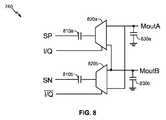
図8は、本発明の例示的な実施形態による、図1のワイヤレス電力伝達システムに使用され得る混合器740の機能ブロック図である。混合器740は、たとえば、混合器740aおよび740bを実装するまたは含むことができる。図示の実施形態では、混合器740は入力SP、SN、およびI/Qを受信し、2つの入力キャパシタ810aおよび810bと、2つのmux 820aおよび820bと、2つの出力キャパシタ830aおよび830bとを含む。 FIG. 8 is a functional block diagram of a
入力SPおよびSNは測定信号であり得る。様々な実施形態では、たとえば、SPおよびSNは、図7に示すノードASPおよびASN、ならびに/またはBSPおよびBSNを表すことができる。入力I/Q(およびその補足物)は、たとえば、直交位相クロック生成器710(図7)から受信され得る。 Inputs SP and SN may be measurement signals. In various embodiments, for example, SP and SN may represent nodes ASP and ASN and / or BSP and BSN shown in FIG. Input I / Q (and its complement) may be received, for example, from quadrature clock generator 710 (FIG. 7).
入力キャパシタ810aおよび810bは各々、入力電圧SPおよびSNを低下させるように構成された、それぞれの高インピーダンス分割器の一部分を形成することができる。一実施形態では、入力キャパシタ810aは、ASPを低下させるように構成された電圧分割器の一部分を形成することができる。入力キャパシタ810bは、ASNを低下させるように構成された電圧分割器の一部分を形成することができる。また、入力キャパシタは、インダクタまたは抵抗器などのいずれかの任意のインピーダンスとして具現化され得る。
mux 820aおよび820bは、RF入力SPおよびSNを直交位相クロック生成器710(図7)からのI/Q局部発振器入力と混合して、差動出力MoutAおよびMoutBを生成するように働く。たとえば、送信フィルタ730(図7)の出力からの信号ASP、ASNは、高インピーダンスキャパシタ810aおよび810bを介してmux 820aおよび820bに結合され得る。クロックI/Qは、電圧の正側または負側のいずれかを選択することによって、入力信号SP/SNを逓倍する。
図9は、本発明の別の例示的な実施形態による、図1のワイヤレス電力伝達システムに使用され得る送信回路900の一部分の機能ブロック図である。送信回路900は、ノードAおよびBと、測定キャパシタCMと、リアクタンスネットネットワーク910と、送信コイルLTXとを含むことができる。リアクタンスネットワーク910は、ノードV2と、インピーダンス要素Z1、Z2、およびZ3とを含む「Y」ネットワークに簡略化されたものとしてモデル化され得る。リアクタンスネットワーク910は、パッシブネットワークまたはアクティブに切り替えられるネットワークであり得る。FIG. 9 is a functional block diagram of a portion of a
送信回路900は、図7に示す送信回路700の態様をモデル化することができる。たとえば、ノードAおよびBはそれぞれ、ノードASPおよびBSP(図7)に対応することができる。測定キャパシタCMは、正測定キャパシタCMP(図7)に対応することができる。リアクタンスネットワーク910は、直列キャパシタCSP(図7)に対応する。別の例として、ノードAおよびBはそれぞれ、ノードASNおよびBSN(図7)に対応することができる。測定キャパシタCMは、負測定キャパシタCMN(図7)に対応することができる。リアクタンスネットワーク910は、直列キャパシタCSN(図7)に対応する。The
一実施形態では、プロセッサ780(図7)は、接点解析を使用して負荷電流(iL)を計算することができる。ノードBにおける電圧は、混合器回路740aおよび/または740b(図7)を使用して測定され得、iCMは本明細書で説明するように計算される。
Yネットワーク(V2)の中央ノードにおける電圧は、式6に示すように、ノードBにおける電圧からZ1を通ったiCMの電圧ドロップを減じたものである。
V2 = VB - iCMZ1...(6)In one embodiment, processor 780 (FIG. 7) can calculate load current (iL ) using contact analysis. The voltage at node B can be measured using
The voltage at the central node of the Y network (V2), as shown in Equation 6 is minus the voltage drop of iCM having passed through the Z1 from the voltage at node B.
V2 = VB -iCM Z1 ... (6)
負荷電流は、式7に示すように、シャントインピーダンスZ2がYネットワークの中央におけるソース電流を低減した後に残るものである。 The load current remains after shunt impedance Z2 reduces the source current at the center of the Y network, as shown in Equation 7.
式7の分子に式6を代入し、項を再整理すると、式8になる。 Substituting Equation 6 into the numerator of Equation 7 and rearranging the terms yields Equation 8.
Z項は、iCMおよびVBを乗算する固定定数として構成され得る。iCMを乗算する項は、式9に示すように、無名数とすることができ、事前計算され得る。The Z term may be configured as a fixed constant that multiplies iCM and VB. The term that multiplies iCM can be anonymous and can be precomputed, as shown in Equation 9.
VB項の乗数は、式10に示すように、アドミタンスと見なすことができる。Xは、特定のネットワーク構成のアドミタンス値と呼ぶことができる。The multiplier of the VB term can be regarded as admittance as shown in Equation 10. X can be referred to as the admittance value for a particular network configuration.
上記で得られた係数を使用して、プロセッサ780(図7)は、式8から式10を組み合わせることによって、負荷電流の実数成分および虚数成分を求めることができる。実数部分を式11に示す。負荷電流の虚数部分を式12に示す。
RE{iL} = RE{iCM}RE{K1x} + IM{VMB}IM{Yx} - IM{iCM}IM{K1x} - RE{VMB}RE{Yx}…(11)
IM{iL} = RE{iCM}IM{K1x} + IM{iCM}RE{K1x} - RE{VMB}IM{Yx} - IM{VMB}RE{Yx}...(12)Using the coefficients obtained above, processor 780 (FIG. 7) can determine the real and imaginary components of the load current by combining equations 8-10. The real part is shown in Equation 11. Equation 12 shows the imaginary part of the load current.
RE {iL } = RE {iCM } RE {K1 x} + IM {VMB } IM {Yx }-IM {iCM } IM {K1x }-RE {VMB } RE {Yx } … (11)
IM {iL } = RE {iCM } IM {K1x } + IM {iCM } RE {K1x }-RE {VMB } IM {Yx }-IM {VMB } RE {Yx }. .. (12)
式13に示すように、実数部分および虚数部分を組み合わせて、負荷電流の大きさを求めることができる。 As shown in Expression 13, the magnitude of the load current can be obtained by combining the real part and the imaginary part.
負荷における電圧は、式14に示すように、Z3にわたる電圧ドロップをV2から減算することによって計算され得る。
VL = V2 - iLZ3...(14)The voltage at the load, as shown in Equation 14 can be calculated by subtracting the voltage drop across Z3 from V2.
VL = V2 -iL Z3 ... (14)
式14および式8を組み合わせると、式15になる。 Combining Equation 14 and Equation 8 yields Equation 15.
Z項を組み合わせて、測定された電流値および電圧値で乗算するための係数にすることができる。リアクタンスネットワーク910の特定の構成を示すXを使用して、複合電圧係数を式16に示す。電流係数を式17に示す。 The Z terms can be combined into a coefficient for multiplying by the measured current and voltage values. The composite voltage coefficient is shown in Equation 16 using X, which represents a particular configuration of the
したがって、プロセッサ780は、式18に従って負荷電圧の実数部分を求めることができる。プロセッサ780は、式19に従って負荷電圧の虚数部分を求めることができる。
RE{VL} = RE{VB}RE{K2x}- IM{VB}IM{K2x} - RE{iCM}RE{ZYx} + IM{iCM}IM{ZYx}…(18)
IM{VL} = RE{VB}IM{K2x} + IM{VB}RE{K2x} - RE{iCM}IM{ZYx} - IM{iCM}RE{ZYx}...(19)Accordingly, the
RE {VL } = RE {VB } RE {K2 x}-IM {VB } IM {K2 x}-RE {iCM } RE {ZYx } + IM {iCM } IM {ZYx } ... (18)
IM {VL } = RE {VB } IM {K2 x} + IM {VB } RE {K2 x}-RE {iCM } IM {ZYx }-IM {iCM } RE {ZYx } ... (19)
共振器の中を見る(looking into)インピーダンスは、オームの法則ならびに電力測定用にすでにサンプリングされた複合電圧および電流を使用して計算され得る。したがって、プロセッサ780は、式20に従って送信コイルLTXのインピーダンスを求め、式21に従って負荷の実数部分を求め、式22に従って負荷の虚数部分を求めることができる。The impedance looking into the resonator can be calculated using Ohm's law and the combined voltage and current already sampled for power measurement. Accordingly, the
図10は、ワイヤレス電力送信の例示的な方法のフローチャート1000である。図1〜図2に関して上記で説明したワイヤレス電力伝達システム100、図4に関して上記で説明した送信機404、および図7に関して上記で説明した送信回路700を参照しながらフローチャート1000の方法について本明細書で説明するが、フローチャート1000の方法は、本明細書で説明する別のデバイス、または任意の他の適切なデバイスによって実装され得ることを当業者は諒解されよう。一実施形態では、フローチャート1000内のステップは、たとえば、コントローラ415(図4)、プロセッサシグナリングコントローラ516(図5)および/またはプロセッサ780(図7)などの、プロセッサまたはコントローラによって実施することができる。フローチャート1000の方法は、特定の順序を参照して本明細書に記載されるが、様々な実施形態では、本明細書のブロックが異なる順序で実施されるか、または省略される場合があり、かつさらなるブロックが追加される場合がある。 FIG. 10 is a
最初に、ブロック1010で、プロセッサ780は、直列要素の第1の端子における第1の電圧の実数成分および虚数成分を求める。直列要素は、直列要素CMPおよびCMNなどの、送信コイルに電気的に結合された測定キャパシタであり得る。たとえば、プロセッサ780は、I信号およびQ信号を混合器740aに連続的に出力するように直交位相クロック生成器710を制御することができる。したがって、混合器740aは、ノードASPおよびASNにおける電圧信号の実数成分および虚数成分を出力することができる。一実施形態では、直列要素は、たとえば、送信フィルタ730中の構成要素などの、抵抗器またはインダクタを含むことができる。一実施形態では、第1の電圧は差動電圧であり得る。Initially, at
次に、ブロック1020で、プロセッサ780は、直列要素の第2の端子における第2の電圧の実数成分および虚数成分を求める。たとえば、プロセッサ780は、I信号およびQ信号を混合器740bに連続的に出力するように直交位相クロック生成器710を制御することができる。したがって、混合器740bは、ノードBSPおよびBSNにおける電圧信号の実数成分および虚数成分を出力することができる。一実施形態では、第2の電圧は差動電圧であり得る。 Next, at
様々な実施形態では、加算増幅器750aおよび750bは、混合器740aおよび740bから受信された実数成分と虚数成分との間の和および/または差を出力することができる。LPF 760aおよび760bは、加算増幅器750aおよび750bの出力をフィルタリングすることができる。ADC 770aおよび770bは、LPF 760aおよび760bの出力を、プロセッサ780に与えられるデジタル値に変換することができる。プロセッサ780は値をスケーリングすることができる。 In various embodiments, summing
次いで、ブロック1030で、プロセッサ780は、測定された第1の電圧および第2の電圧に基づいて、直列要素を通る電流の実数成分および虚数成分を求める。たとえば、プロセッサ780は直列要素CMPおよびCMNの値を知ることができ、これらの値をメモリに記憶するか、較正するか、または動的に求めることができる。プロセッサ780は、オームの法則の複素形式に従って電流を計算することができる。Next, at
その後、ブロック1040で、プロセッサ780は、測定された電圧および求められた電流に基づいて、送信特性を求める。たとえば、プロセッサ780は、式22の電力ベクトルを使用して送信電力を計算することができ、式中、I*は測定された電流のRMS値の共役複素数である。一実施形態では、プロセッサ780は、図11に関して以下で説明するように、Z=V/Iと同じパラメータを使用して動作周波数における複素インピーダンスを計算することができる。Thereafter, at
様々な実施形態では、プロセッサ780は電力ベクトルを実数成分および虚数成分に分解することができる。プロセッサ780は、電圧および電流のRMS値を計算し、スケールファクタおよび/または類似の処理を適用することができる。同様に、プロセッサ780はベクトルデータを使用して、既知の成分値に基づいて、回路中の任意のポイントにおけるインピーダンス、電流、および電圧を計算することができる。したがって、送信されたワイヤレス電力およびワイヤレス負荷インピーダンスは、損失および送信コイルLTXを介して結合されたリアクタンスとして解かれ得る。In various embodiments, the
次に、ブロック1050で、プロセッサ780は、計算された送信特性に基づいて、ワイヤレス電力送信の特性を調整する。たとえば、プロセッサ780は、意図しない受信機が送信コイルLTXに近いと判断することができる。プロセッサ780は、計算された送信特性を比較して、1つまたは複数の許可されたまたは登録された受信機によって報告された電力を受信することができる。様々な実施形態では、プロセッサ780は、計算された送信特性に基づいて、送信特性を上げる、下げる、またはさもなければ変更することができる。Next, at
図11は、本発明の一実施形態による、送信特性を検出するための装置1100の機能ブロック図である。ワイヤレス通信のための装置は、図11に示す簡略化された装置1100よりも多くの構成要素を有し得ることを、当業者は諒解されよう。送信特性を検出するための装置1100は、特許請求の範囲内の実装形態のいくつかの顕著な特徴を説明するのに有用なこれらの構成要素のみを含む。送信特性を検出するための装置1100は、直列要素の第1の端子における第1の電圧の実数成分および虚数成分を求めるための手段1110と、直列要素の第2の端子における第2の電圧の実数成分および虚数成分を求めるための手段1120と、測定された第1の電圧および第2の電圧に基づいて、直列要素を通る電流の実数成分および虚数成分を求めるための手段1130と、測定された電圧および求められた電流に基づいて送信特性を求めるための手段1140と、計算された送信特性に基づいてワイヤレス電力送信の特性を調整するための手段1150とを含む。 FIG. 11 is a functional block diagram of an
一実施形態では、直列要素の第1の端子における第1の電圧の実数成分および虚数成分を求めるための手段1110は、ブロック1010(図10)に関して上記で説明した機能のうちの1つまたは複数を実施するように構成され得る。様々な実施形態では、直列要素の第1の端子における第1の電圧の実数成分および虚数成分を求めるための手段1110は、プロセッサ780(図7)、直交位相クロック生成器710(図7)、キャパシタCMP、CMN、CSPおよび/またはCSN(図7)、混合器740aおよび740b(図7)、加算増幅器750aおよび750b、LPF 760aおよび760b、ならびにADC 770aおよび770bのうちの1つまたは複数によって実装され得る。In one embodiment, the
一実施形態では、直列要素の第2の端子における第2の電圧の実数成分および虚数成分を求めるための手段1120は、ブロック1020(図10)に関して上記で説明した機能のうちの1つまたは複数を実施するように構成され得る。様々な実施形態では、直列要素の第2の端子における第2の電圧の実数成分および虚数成分を求めるための手段1120は、プロセッサ780(図7)、直交位相クロック生成器710(図7)、キャパシタCMP、CMN、CSPおよび/またはCSN(図7)、混合器740aおよび740b(図7)、加算増幅器750aおよび750b、LPF 760aおよび760b、ならびにADC 770aおよび770bのうちの1つまたは複数によって実装され得る。In one embodiment, the
一実施形態では、測定された第1の電圧および第2の電圧に基づいて、直列要素を通る電流の実数成分および虚数成分を求めるための手段1130は、ブロック1030(図10)に関して上記で説明した機能のうちの1つまたは複数を実施するように構成され得る。様々な実施形態では、測定された第1の電圧および第2の電圧に基づいて、直列要素を通る電流の実数成分および虚数成分を求めるための手段1130は、プロセッサ780(図7)、コントローラ415(図4)、およびメモリ470(図4)のうちの1つまたは複数によって実装され得る。 In one embodiment, means 1130 for determining the real and imaginary components of the current through the series element based on the measured first and second voltages is described above with respect to block 1030 (FIG. 10). May be configured to perform one or more of the functions performed. In various embodiments, the
一実施形態では、測定された電圧および求められた電流に基づいて送信特性を求めるための手段1140は、ブロック1040(図10)に関して上記で説明した機能のうちの1つまたは複数を実施するように構成され得る。様々な実施形態では、測定された電圧および求められた電流に基づいて送信特性を求めるための手段1140は、プロセッサ780(図7)、コントローラ415(図4)、およびメモリ470(図4)のうちの1つまたは複数によって実装され得る。 In one embodiment, the
一実施形態では、計算された送信特性に基づいてワイヤレス電力送信の特性を調整するための手段1150は、ブロック1050(図10)に関して上記で説明した機能のうちの1つまたは複数を実施するように構成され得る。様々な実施形態では、計算された送信特性に基づいて、ワイヤレス電力送信の特性を調整するための手段1150は、プロセッサ780(図7)、コントローラ415(図4)、およびメモリ470(図4)のうちの1つまたは複数によって実装され得る。 In one embodiment, the
上記で説明した方法の様々な動作は、様々なハードウェアおよび/またはソフトウェア構成要素、回路、および/またはモジュールなど、それらの動作を実施することが可能な任意の好適な手段によって実施され得る。一般に、図に示される任意の動作は、動作を実施することができる対応する機能手段によって実施することができる。 The various operations of the methods described above may be performed by any suitable means capable of performing those operations, such as various hardware and / or software components, circuits, and / or modules. In general, any operations shown in the figures can be performed by corresponding functional means capable of performing the operations.
多種多様な技術および技法のうちのいずれかを使用して情報および信号を表すことができる。たとえば、上記の説明全体にわたって参照される場合があるデータ、命令、コマンド、情報、信号、ビット、シンボル、およびチップは、電圧、電流、電磁波、磁界もしくは磁性粒子、光場もしくは光学粒子、またはそれらの任意の組合せによって表すことができる。 Information and signals can be represented using any of a wide variety of techniques and techniques. For example, data, instructions, commands, information, signals, bits, symbols, and chips that may be referred to throughout the above description are voltages, currents, electromagnetic waves, magnetic fields or magnetic particles, light fields or optical particles, or Can be represented by any combination of
本明細書で開示する実施形態に関して説明する様々な例示的な論理ブロック、モジュール、回路、およびアルゴリズムステップは、電子ハードウェア、コンピュータソフトウェア、またはその両方の組合せとして実装され得る。ハードウェアおよびソフトウェアのこの互換性を明確に示すために、様々な例示的な構成要素、ブロック、モジュール、回路、およびステップについて、上記では概してそれらの機能性に関して説明した。そのような機能性をハードウェアとして実装するか、またはソフトウェアとして実装するかは、特定の適用例および全体的なシステムに課される設計制約に依存する。説明した機能性は、特定の適用例ごとに様々な方法で実装することができるが、そのような実装の決定は、本発明の実施形態の範囲からの逸脱を引き起こすと解釈すべきではない。 Various exemplary logic blocks, modules, circuits, and algorithm steps described with respect to the embodiments disclosed herein may be implemented as electronic hardware, computer software, or a combination of both. To clearly illustrate this interchangeability of hardware and software, various illustrative components, blocks, modules, circuits, and steps have been described above generally in terms of their functionality. Whether such functionality is implemented as hardware or software depends upon the particular application and design constraints imposed on the overall system. Although the described functionality can be implemented in a variety of ways for a particular application, such implementation decisions should not be construed as causing deviations from the scope of embodiments of the invention.
本明細書で開示する実施形態に関して説明する様々な例示的なブロック、モジュール、および回路は、汎用プロセッサ、デジタルシグナルプロセッサ(DSP)、特定用途向け集積回路(ASIC)、フィールドプログラマブルゲートアレイ(FPGA)もしくは他のプログラマブル論理デバイス、個別ゲートもしくはトランジスタ論理、個別ハードウェア構成要素、または、本明細書で説明する機能を実施するように設計されたそれらの任意の組合せで、実装または実施されてよい。汎用プロセッサはマイクロプロセッサであり得るが、代替として、プロセッサは、任意の従来のプロセッサ、コントローラ、マイクロコントローラ、または状態機械であり得る。プロセッサはまた、コンピューティングデバイスの組合せ、たとえば、DSPとマイクロプロセッサとの組合せ、複数のマイクロプロセッサ、DSPコアと連携する1つもしくは複数のマイクロプロセッサ、または任意の他のそのような構成として実装することができる。 Various exemplary blocks, modules, and circuits described with respect to the embodiments disclosed herein include general purpose processors, digital signal processors (DSPs), application specific integrated circuits (ASICs), field programmable gate arrays (FPGAs). Or may be implemented or implemented in other programmable logic devices, individual gate or transistor logic, individual hardware components, or any combination thereof designed to perform the functions described herein. A general purpose processor may be a microprocessor, but in the alternative, the processor may be any conventional processor, controller, microcontroller, or state machine. The processor is also implemented as a combination of computing devices, eg, a DSP and microprocessor combination, a plurality of microprocessors, one or more microprocessors associated with a DSP core, or any other such configuration. be able to.
本明細書で開示された実施形態に関連して記載された方法またはアルゴリズムおよび機能のステップは、直接ハードウェアで具現化されても、プロセッサによって実行されるソフトウェアモジュールで具現化されても、またはその2つの組合せで具現化されてもよい。ソフトウェアで実装される場合、機能は、1つまたは複数の命令またはコードとして、有形な非一時的コンピュータ可読媒体上に記憶すること、または有形な非一時的コンピュータ可読媒体を介して送信することができる。ソフトウェアモジュールは、ランダムアクセスメモリ(RAM)、フラッシュメモリ、読取り専用メモリ(ROM)、電気的にプログラム可能なROM(EPROM)、電気的に消去可能およびプログラム可能なROM(EEPROM)、レジスタ、ハードディスク、着脱可能ディスク、CD ROM、または当技術分野で知られた任意の他の形態の記憶媒体内に存在することができる。記憶媒体は、プロセッサが記憶媒体から情報を読み取り、記憶媒体に情報を書き込むことができるように、プロセッサに結合される。代替形態では、記憶媒体はプロセッサと一体にすることができる。本明細書で使用する場合、ディスク(disk)およびディスク(disc)は、コンパクトディスク(CD)、レーザーディスク(登録商標)、光ディスク、デジタル多用途ディスク(DVD)、フロッピー(登録商標)ディスク、およびブルーレイディスクを含み、ディスク(disk)は、通常、磁気的にデータを再生し、ディスク(disc)は、レーザーで光学的にデータを再生する。上記の組合せも、コンピュータ可読媒体の範囲の中に含まれるべきである。プロセッサおよび記憶媒体は、ASIC中に常駐し得る。ASICは、ユーザ端末内に常駐し得る。代替形態では、プロセッサおよび記憶媒体は、ユーザ端末内に個別構成要素として存在することができる。 The method or algorithm and functional steps described in connection with the embodiments disclosed herein may be implemented directly in hardware, implemented in software modules executed by a processor, or It may be embodied by a combination of the two. If implemented in software, the functions may be stored on or transmitted over a tangible non-transitory computer readable medium as one or more instructions or code. it can. Software modules include random access memory (RAM), flash memory, read only memory (ROM), electrically programmable ROM (EPROM), electrically erasable and programmable ROM (EEPROM), registers, hard disk, It may reside on a removable disk, CD ROM, or any other form of storage medium known in the art. A storage medium is coupled to the processor such that the processor can read information from, and write information to, the storage medium. In the alternative, the storage medium may be integral to the processor. As used herein, disk and disc are compact disc (CD), laser disc (registered trademark), optical disc, digital versatile disc (DVD), floppy (registered trademark) disc, and Including Blu-ray discs, the disk normally reproduces data magnetically, and the disc optically reproduces data with a laser. Combinations of the above should also be included within the scope of computer-readable media. The processor and the storage medium can reside in an ASIC. The ASIC may reside in the user terminal. In the alternative, the processor and the storage medium may reside as discrete components in a user terminal.
本開示を要約するために、本明細書において、本発明のいくつかの態様、利点、および新規の特徴が説明されてきた。本発明の任意の特定の実施形態に従って、そのような利点の必ずしもすべてを実現できない場合があることを理解されたい。したがって、本発明は、本明細書で教示された1つの利点または利点のグループを達成または最適化するが、本明細書で教示または提案された可能性のある他の利点を必ずしも達成するとは限らない方法で、具体化または実施することができる。 To summarize the present disclosure, several aspects, advantages and novel features of the present invention have been described herein. It should be understood that not all such advantages may be realized in accordance with any particular embodiment of the present invention. Thus, while the present invention achieves or optimizes one advantage or group of advantages taught herein, it does not necessarily achieve other advantages that may have been taught or suggested herein. Can be implemented or implemented in a non-existent manner.
上述の実施形態への様々な修正が容易に明らかになり、本明細書に定義する一般原理は、本発明の趣旨または範囲を逸脱することなく他の実施形態に適用され得る。したがって、本発明は、本明細書に示された実施形態に限定されるものではなく、本明細書に開示された原理および新規の特徴に一致する最大の範囲を与えるものである。 Various modifications to the above-described embodiments will be readily apparent and the general principles defined herein may be applied to other embodiments without departing from the spirit or scope of the invention. Accordingly, the present invention is not limited to the embodiments shown herein, but provides the greatest scope consistent with the principles and novel features disclosed herein.
100 ワイヤレス電力伝達システム、ワイヤレス電力送信システム
102 入力電力
104 送信機
105 場
108 受信機
110 出力電力
114 送信コイル
118 受信コイル
204 送信機
205 ワイヤレス場
206 送信回路
208 受信機
210 受信回路
214 送信コイル、TXコイル
218 受信コイル、RXコイル
219 通信チャネル
222 発振器
223 周波数制御信号
224 ドライバ回路
226 フィルタ/整合回路
232 整合回路
234 整流器/スイッチング回路
236 バッテリー
350 送信回路、受信回路
352 送信コイル、受信コイル、コイル、ループアンテナ、空芯ループコイル
354 キャパシタ
356 キャパシタ
358 信号
404 送信機
406 送信回路
408 ローパスフィルタ(LPF)、フィルタ
409 固定インピーダンス整合回路、整合回路
414 送信コイル、コイル
415 コントローラ、プロセッサ
416 負荷感知回路
423 発振器
424 ドライバ回路、送信機ドライバ回路、PA
460 密閉型検出器
480 存在検出器
490 電力検出器
506 電力変換回路
508 受信機、ワイヤレス電力受信機
510 受信回路
512 スイッチング回路
514 信号伝達検出器/ビーコン回路
516 プロセッサ、プロセッサシグナリングコントローラ
518 受信コイル
520 RF-DC変換器
522 DC-DC変換器
550 デバイス、充電デバイス
600 送信回路
602 入力信号
614 コイル、送信コイル
620 キャパシタンス
622 可変抵抗器
624 ドライバ回路
626 フィルタ回路、ローパスフィルタ回路
632 インダクタ
634 キャパシタ
636 キャパシタ
650 送信回路
700 送信回路
710 直交位相クロック生成器
720 送信増幅器
730 送信フィルタ、整合回路
740a、740b 差動混合器、混合器回路
750a、750b 加算増幅器
760a、760b ローパスフィルタ(LPF)
770a、770b アナログデジタル変換器(ADC)
780 プロセッサ
810a、810b 入力キャパシタ
820a、820b mux
830a、830b 出力キャパシタ
900 送信回路
910 リアクタンスネットワーク
1000 フローチャート
1100 装置
1120 手段
1130 手段
1140 手段
1150 手段
A、B、V2 ノード
CM 測定キャパシタ
CMP 正測定キャパシタ
CMN 負測定キャパシタ
CP 並列キャパシタ
CSP 正直列キャパシタ
CSN 負直列キャパシタ
LTX 送信コイル
Z1、Z2、Z3 インピーダンス要素
ZM 直列要素100 wireless power transfer system, wireless power transmission system
102 Input power
104 transmitter
105 places
108 Receiver
110 Output power
114 Transmitting coil
118 Receiver coil
204 Transmitter
205 Wireless field
206 Transmitter circuit
208 receiver
210 Receiver circuit
214 Transmitting coil, TX coil
218 Receiver coil, RX coil
219 communication channel
222 Oscillator
223 Frequency control signal
224 Driver circuit
226 Filter / matching circuit
232 matching circuit
234 Rectifier / Switching circuit
236 battery
350 Transmitter circuit, receiver circuit
352 Transmitting coil, receiving coil, coil, loop antenna, air core loop coil
354 capacitors
356 capacitors
358 signals
404 transmitter
406 Transmitter circuit
408 Low-pass filter (LPF), filter
409 Fixed impedance matching circuit, matching circuit
414 Transmitting coil, coil
415 Controller, processor
416 Load sensing circuit
423 oscillator
424 Driver circuit, transmitter driver circuit, PA
460 Sealed detector
480 Presence detector
490 Power detector
506 Power conversion circuit
508 receiver, wireless power receiver
510 Receiver circuit
512 switching circuit
514 Signal detector / beacon circuit
516 processor, processor signaling controller
518 Receiver coil
520 RF-DC converter
522 DC-DC converter
550 devices, charging devices
600 Transmitter circuit
602 Input signal
614 coil, transmitter coil
620 capacitance
622 variable resistor
624 Driver circuit
626 Filter circuit, low-pass filter circuit
632 inductor
634 capacitors
636 capacitor
650 transmitter circuit
700 Transmitter circuit
710 quadrature clock generator
720 transmit amplifier
730 Transmit filter, matching circuit
740a, 740b differential mixer, mixer circuit
750a, 750b summing amplifier
760a, 760b Low-pass filter (LPF)
770a, 770b Analog-to-digital converter (ADC)
780 processor
810a, 810b input capacitor
820a, 820b mux
830a, 830b Output capacitor
900 Transmitter circuit
910 Reactance Network
1000 Flowchart
1100 equipment
1120 means
1130 means
1140 means
1150 means
A, B, V2 nodes
CM measuring capacitor
CMP positive measurement capacitor
CMN negative measurement capacitor
CP parallel capacitor
CSP positive series capacitor
CSN negative series capacitor
LTX transmitter coil
Z1 , Z2 , Z3 impedance elements
ZM series element
Claims (42)
Translated fromJapanese前記直列要素の第1の端子における第1の電圧の実数成分および虚数成分を求めるステップと、
前記直列要素の第2の端子における第2の電圧の実数成分および虚数成分を求めるステップと、
前記測定された第1の電圧および第2の電圧に基づいて、前記直列要素を通る電流の実数成分および虚数成分を求めるステップと、
前記測定された電圧および求められた電流に基づいて、送信特性を求めるステップと、
計算された送信特性に基づいて、ワイヤレス電力送信の特性を調整するステップと
を含む方法。A method for detecting transmission characteristics in a wireless power transmission device including a series element electrically coupled to a transmission coil comprising:
Obtaining a real component and an imaginary component of the first voltage at the first terminal of the series element;
Obtaining a real component and an imaginary component of the second voltage at the second terminal of the series element;
Determining a real component and an imaginary component of the current through the series element based on the measured first voltage and second voltage;
Determining transmission characteristics based on the measured voltage and the determined current;
Adjusting the characteristics of the wireless power transmission based on the calculated transmission characteristics.
ワイヤレス電力を送信するように構成された送信コイルと、
同相(I)クロック信号および直交位相(Q)クロック信号を生成するように構成された直交位相クロック生成器と、
前記送信コイルに電気的に結合され、第1の端子またはポートおよび第2の端子またはポートを含む直列要素と、
前記直列要素の前記第1の端子またはポートおよび前記第2の端子またはポートにおける少なくとも1つの信号を前記I信号および前記Q信号のうちの1つで乗算するように構成された混合器または混合器のセットと
を含む、ワイヤレスデバイス。A wireless device configured to provide wireless power to a receiver,
A transmit coil configured to transmit wireless power;
A quadrature clock generator configured to generate an in-phase (I) clock signal and a quadrature (Q) clock signal;
A series element electrically coupled to the transmitter coil and including a first terminal or port and a second terminal or port;
A mixer or mixer configured to multiply at least one signal at the first terminal or port and the second terminal or port of the series element by one of the I signal and the Q signal A wireless device including a set of.
前記直列要素の第1の端子における第1の電圧の実数成分および虚数成分を求めるための手段と、
前記直列要素の第2の端子における第2の電圧の実数成分および虚数成分を求めるための手段と、
前記測定された第1の電圧および第2の電圧に基づいて、前記直列要素を通る電流の実数成分および虚数成分を求めるための手段と、
前記測定された電圧および求められた電流に基づいて、送信特性を求めるための手段と、
計算された送信特性に基づいて、ワイヤレス電力送信の特性を調整するための手段と
を含む装置。An apparatus for detecting transmission characteristics in a wireless power transmission device including a series element electrically coupled to a transmission coil, comprising:
Means for determining a real component and an imaginary component of the first voltage at the first terminal of the series element;
Means for determining a real component and an imaginary component of the second voltage at the second terminal of the series element;
Means for determining real and imaginary components of the current through the series element based on the measured first voltage and second voltage;
Means for determining a transmission characteristic based on the measured voltage and the determined current;
Means for adjusting the characteristics of the wireless power transmission based on the calculated transmission characteristics.
送信コイルに電気的に結合された直列要素の第1の端子における第1の電圧の実数成分および虚数成分を求めさせ、
前記直列要素の第2の端子における第2の電圧の実数成分および虚数成分を求めさせ、
前記測定された第1の電圧および第2の電圧に基づいて、前記直列要素を通る電流の実数成分および虚数成分を求めさせ、
前記測定された電圧および求められた電流に基づいて、送信特性を求めさせ、
計算された送信特性に基づいて、ワイヤレス電力送信の特性を調整させる、
非一時的コンピュータ可読媒体。A non-transitory computer-readable medium containing code, wherein when the code is executed, the device includes:
Determining the real and imaginary components of the first voltage at the first terminal of the series element electrically coupled to the transmit coil;
The real component and the imaginary component of the second voltage at the second terminal of the series element are obtained,
Based on the measured first voltage and second voltage, let the real and imaginary components of the current through the series element be determined,
Based on the measured voltage and the determined current, to determine the transmission characteristics,
Based on the calculated transmission characteristics, adjust the characteristics of wireless power transmission,
Non-transitory computer readable medium.
Applications Claiming Priority (5)
| Application Number | Priority Date | Filing Date | Title |
|---|---|---|---|
| US201261707743P | 2012-09-28 | 2012-09-28 | |
| US61/707,743 | 2012-09-28 | ||
| US13/801,981 | 2013-03-13 | ||
| US13/801,981US9190876B2 (en) | 2012-09-28 | 2013-03-13 | Systems and methods for detecting wireless charging transmit characteristics |
| PCT/US2013/060676WO2014052161A1 (en) | 2012-09-28 | 2013-09-19 | Systems and methods for detecting wireless charging transmit characteristics |
Publications (2)
| Publication Number | Publication Date |
|---|---|
| JP2015537497Atrue JP2015537497A (en) | 2015-12-24 |
| JP6227656B2 JP6227656B2 (en) | 2017-11-08 |
Family
ID=50384492
Family Applications (1)
| Application Number | Title | Priority Date | Filing Date |
|---|---|---|---|
| JP2015534564AActiveJP6227656B2 (en) | 2012-09-28 | 2013-09-19 | System and method for detecting wireless charging transmission characteristics |
Country Status (10)
| Country | Link |
|---|---|
| US (1) | US9190876B2 (en) |
| EP (1) | EP2901564B1 (en) |
| JP (1) | JP6227656B2 (en) |
| KR (1) | KR101788947B1 (en) |
| CN (1) | CN104685797B (en) |
| BR (1) | BR112015006963B1 (en) |
| ES (1) | ES2699405T3 (en) |
| HU (1) | HUE040134T2 (en) |
| TW (1) | TWI515992B (en) |
| WO (1) | WO2014052161A1 (en) |
Cited By (2)
| Publication number | Priority date | Publication date | Assignee | Title |
|---|---|---|---|---|
| JP2019013100A (en)* | 2017-06-30 | 2019-01-24 | 学校法人立命館 | Wireless power supply system |
| JP2020532269A (en)* | 2017-08-28 | 2020-11-05 | エフィシエント パワー コンヴァーション コーポレーション | Multi-coil large area wireless power system |
Families Citing this family (45)
| Publication number | Priority date | Publication date | Assignee | Title |
|---|---|---|---|---|
| US10355526B2 (en)* | 2008-11-26 | 2019-07-16 | Auckland Uniservices Limited | Bi-directional inductive power transfer |
| CN108173350B (en) | 2012-05-02 | 2021-06-15 | 苹果公司 | Inductive power transmitter and method for detecting and identifying receiver |
| KR20210096686A (en) | 2012-11-05 | 2021-08-05 | 애플 인크. | Inductively coupled power transfer systems |
| US20150091523A1 (en)* | 2013-10-02 | 2015-04-02 | Mediatek Singapore Pte. Ltd. | Wireless charger system that has variable power / adaptive load modulation |
| DE102014207062A1 (en)* | 2014-04-11 | 2015-10-15 | Bayerische Motoren Werke Aktiengesellschaft | Combined surface heating |
| EP3158621A4 (en)* | 2014-06-20 | 2017-07-12 | PowerbyProxi Limited | Foreign object detection in inductive power transfer field |
| US10749380B2 (en)* | 2014-09-23 | 2020-08-18 | Integrated Device Technology, Inc. | Apparatuses and related methods for generating wireless status indications for a wireless power transfer system |
| US9612296B2 (en) | 2014-10-08 | 2017-04-04 | Qualcomm Incorporated | Methods and apparatus for testing of wireless power transmitters and systems |
| US9983300B2 (en) | 2014-10-17 | 2018-05-29 | Qualcomm Incorporated | Systems, methods, and apparatus for living object protection in wireless power transfer applications |
| CN107112787A (en)* | 2014-11-11 | 2017-08-29 | 鲍尔拜普罗克西有限公司 | Induced power transmitter |
| JP6406225B2 (en)* | 2015-01-30 | 2018-10-17 | 株式会社デンソー | Non-contact power feeding device |
| WO2016121383A1 (en)* | 2015-01-30 | 2016-08-04 | 株式会社デンソー | Non-contact power-supply device |
| EP3266092B1 (en) | 2015-03-04 | 2020-06-03 | Apple Inc. | Inductive power transmitter |
| CN107529346B (en) | 2015-04-02 | 2021-03-02 | 苹果公司 | Inductive power transmitter |
| KR20160143044A (en)* | 2015-06-04 | 2016-12-14 | 엘지이노텍 주식회사 | Wireless Power Transfer System and Operating method thereof |
| US10277062B2 (en) | 2015-07-30 | 2019-04-30 | Qualcomm Incorporated | System and method for detecting and characterizing an object for wireless charging |
| US20170063158A1 (en)* | 2015-08-24 | 2017-03-02 | Pabellon, Inc | Wireless Power Transfer |
| US20170085113A1 (en)* | 2015-09-22 | 2017-03-23 | Intel Corporation | Constant current radio frequency generator for a wireless charging system |
| KR102130791B1 (en) | 2015-11-19 | 2020-07-06 | 애플 인크. | Induction power transmitter |
| WO2017176128A1 (en) | 2016-04-04 | 2017-10-12 | Powerbyproxi Limited | Inductive power transmitter |
| KR101842712B1 (en)* | 2016-04-14 | 2018-03-29 | 주식회사 맵스 | Monitoring apparatus and method for wireless power transmitter |
| EP4007121A1 (en)* | 2016-05-27 | 2022-06-01 | WiTricity Corporation | Voltage regulation in wireless power receivers |
| KR20180057419A (en)* | 2016-11-22 | 2018-05-30 | 삼성전기주식회사 | Apparatus and method for measuring ac power |
| US10804748B2 (en) | 2016-12-14 | 2020-10-13 | Apple Inc. | Wireless power system with foreign object detection |
| KR102257764B1 (en)* | 2017-02-22 | 2021-05-28 | 삼성전자주식회사 | Near field communication device |
| US10187122B2 (en)* | 2017-02-22 | 2019-01-22 | Samsung Electronics Co., Ltd. | Near field communications device |
| US10283952B2 (en) | 2017-06-22 | 2019-05-07 | Bretford Manufacturing, Inc. | Rapidly deployable floor power system |
| WO2019006376A1 (en)* | 2017-06-29 | 2019-01-03 | Witricity Corporation | Protection and control of wireless power systems |
| KR102419350B1 (en)* | 2017-11-08 | 2022-07-12 | 한국전자통신연구원 | Apparatus for transmmiting wireless power and apparatus for receiving wireless power |
| US11001159B2 (en) | 2018-02-20 | 2021-05-11 | Witricity Corporation | Fault detection and monitoring methods for safe operation of a WEVC system |
| CN113169587B (en) | 2018-11-30 | 2022-04-15 | 韦特里西提公司 | System and method for low power excitation in high power wireless power systems |
| US11002874B2 (en)* | 2018-12-21 | 2021-05-11 | Witricity Corporation | Foreign object detection circuit using mutual impedance sensing |
| EP3906617A1 (en) | 2019-01-02 | 2021-11-10 | GE Hybrid Technologies, LLC | Wireless power transmission using multiple transmitters and receivers |
| JP7265735B2 (en)* | 2019-01-24 | 2023-04-27 | イーサーダイン テクノロジーズ インコーポレイテッド | Series distributed radio frequency (RF) generator for use in wireless power transfer |
| CN114144960B (en) | 2019-05-24 | 2024-05-14 | 韦特里西提公司 | Protection circuit for wireless power receiver |
| CN114651381B (en) | 2019-08-26 | 2023-06-23 | 韦特里西提公司 | Active Rectification Control in Wireless Power Systems |
| JP2023500400A (en) | 2019-11-12 | 2023-01-05 | ジーイー・ハイブリッド・テクノロジーズ・エルエルシー | Wireless power transfer using load sharing receiver |
| WO2021154968A1 (en) | 2020-01-29 | 2021-08-05 | Witricity Corporation | Auxiliary power dropout protection for a wireless power transfer system |
| JP7381767B2 (en) | 2020-03-06 | 2023-11-16 | ワイトリシティ コーポレーション | Active rectification in wireless power systems |
| US11764621B1 (en)* | 2021-09-10 | 2023-09-19 | Apple Inc. | Wireless power transfer with integrated communications |
| US12047088B2 (en) | 2021-12-21 | 2024-07-23 | Apple Inc. | Data transfer between analog and digital integrated circuits |
| US12407195B2 (en)* | 2022-09-30 | 2025-09-02 | Nxp B.V. | Method and device for performing a presence check for wireless charging listener devices |
| TWI863572B (en)* | 2023-09-19 | 2024-11-21 | 英業達股份有限公司 | Wireless charging device |
| CN119651934B (en)* | 2025-02-19 | 2025-06-17 | 广东力德诺电子科技有限公司 | A wireless charging receiving system supporting multiple protocols |
| CN120566660A (en)* | 2025-07-30 | 2025-08-29 | 深圳市贝兰德科技有限公司 | Multi-device wireless charging coupling characteristic dynamic detection method |
Citations (11)
| Publication number | Priority date | Publication date | Assignee | Title |
|---|---|---|---|---|
| JPS5679260A (en)* | 1979-12-03 | 1981-06-29 | Anritsu Corp | Measuring apparatus for digital signal selective level |
| JPS63138270A (en)* | 1986-11-28 | 1988-06-10 | Mitsubishi Electric Corp | Difference voltage detecting circuit |
| JP2002062317A (en)* | 2000-08-23 | 2002-02-28 | Toshiba Corp | Capacitor current measuring device |
| US6397157B1 (en)* | 1999-07-02 | 2002-05-28 | General Electric Company | Method and apparatus for real time measurement of three phase electrical parameters |
| JP2008536465A (en)* | 2005-04-12 | 2008-09-04 | シーメンス アクチエンゲゼルシヤフト | Primary part for contactless current supply, monitoring the operating state of the secondary part |
| JP2008278486A (en)* | 2007-04-25 | 2008-11-13 | Seiko Epson Corp | Modulation signal receiving apparatus and amplitude modulation signal demodulation method |
| JP2009089549A (en)* | 2007-10-02 | 2009-04-23 | Panasonic Corp | Charger |
| JP2009112137A (en)* | 2007-10-31 | 2009-05-21 | Meleagros Corp | Power transmission device of power transmission apparatus |
| US20100066349A1 (en)* | 2008-09-12 | 2010-03-18 | University Of Florida Research Foundation, Inc. | Method and Apparatus of Load Detection for a Planar Wireless Power System |
| JP2011507481A (en)* | 2007-12-21 | 2011-03-03 | アクセス ビジネス グループ インターナショナル リミテッド ライアビリティ カンパニー | Inductive power transfer |
| WO2012112703A1 (en)* | 2011-02-17 | 2012-08-23 | Qualcomm Incorporated | Systems and methods for controlling output power of a wireless power transmitter |
Family Cites Families (12)
| Publication number | Priority date | Publication date | Assignee | Title |
|---|---|---|---|---|
| US7586384B2 (en) | 2005-08-15 | 2009-09-08 | Nokia Corporation | Integrated load impedance sensing for tunable matching networks |
| DE102007006394B4 (en) | 2006-11-07 | 2008-08-07 | Schleifring Und Apparatebau Gmbh | Inductive rotary transformer |
| US8072380B2 (en) | 2009-04-10 | 2011-12-06 | Raytheon Company | Wireless power transmission system and method |
| US8450997B2 (en)* | 2009-04-28 | 2013-05-28 | Brown University | Electromagnetic position and orientation sensing system |
| US8233871B2 (en) | 2009-06-16 | 2012-07-31 | California Institute Of Technology | Incompressible RF receiver |
| US9094054B2 (en) | 2009-11-30 | 2015-07-28 | Broadcom Corporation | IC controlled wireless power operation and applications thereof including control channel communication configuration |
| JP5459669B2 (en)* | 2010-03-16 | 2014-04-02 | 株式会社東芝 | Magnetic resonance imaging system |
| US9118217B2 (en) | 2010-09-30 | 2015-08-25 | Broadcom Corporation | Portable computing device with wireless power distribution |
| KR101739293B1 (en) | 2010-12-23 | 2017-05-24 | 삼성전자주식회사 | System for wireless power transmission and reception using in-band communication |
| JP6035711B2 (en)* | 2011-07-21 | 2016-11-30 | ソニー株式会社 | Detection device, power reception device, power transmission device, non-contact power transmission system, and detection method |
| US9071284B2 (en)* | 2011-10-21 | 2015-06-30 | Qualcomm Incorporated | Load impedance detection for static or dynamic adjustment of passive loads |
| CN104272545B (en) | 2011-12-16 | 2018-06-12 | 奥克兰联合服务有限公司 | Inductive power transfer system and method |
- 2013
- 2013-03-13USUS13/801,981patent/US9190876B2/enactiveActive
- 2013-09-19HUHUE13770797Apatent/HUE040134T2/enunknown
- 2013-09-19KRKR1020157010186Apatent/KR101788947B1/enactiveActive
- 2013-09-19WOPCT/US2013/060676patent/WO2014052161A1/enactiveApplication Filing
- 2013-09-19JPJP2015534564Apatent/JP6227656B2/enactiveActive
- 2013-09-19BRBR112015006963-0Apatent/BR112015006963B1/enactiveIP Right Grant
- 2013-09-19CNCN201380049918.9Apatent/CN104685797B/enactiveActive
- 2013-09-19EPEP13770797.2Apatent/EP2901564B1/enactiveActive
- 2013-09-19ESES13770797Tpatent/ES2699405T3/enactiveActive
- 2013-09-27TWTW102135167Apatent/TWI515992B/enactive
Patent Citations (13)
| Publication number | Priority date | Publication date | Assignee | Title |
|---|---|---|---|---|
| JPS5679260A (en)* | 1979-12-03 | 1981-06-29 | Anritsu Corp | Measuring apparatus for digital signal selective level |
| JPS63138270A (en)* | 1986-11-28 | 1988-06-10 | Mitsubishi Electric Corp | Difference voltage detecting circuit |
| US6397157B1 (en)* | 1999-07-02 | 2002-05-28 | General Electric Company | Method and apparatus for real time measurement of three phase electrical parameters |
| JP2003504599A (en)* | 1999-07-02 | 2003-02-04 | ゼネラル・エレクトリック・カンパニイ | Method and apparatus for real-time measurement of three-phase electrical parameters |
| JP2002062317A (en)* | 2000-08-23 | 2002-02-28 | Toshiba Corp | Capacitor current measuring device |
| JP2008536465A (en)* | 2005-04-12 | 2008-09-04 | シーメンス アクチエンゲゼルシヤフト | Primary part for contactless current supply, monitoring the operating state of the secondary part |
| JP2008278486A (en)* | 2007-04-25 | 2008-11-13 | Seiko Epson Corp | Modulation signal receiving apparatus and amplitude modulation signal demodulation method |
| JP2009089549A (en)* | 2007-10-02 | 2009-04-23 | Panasonic Corp | Charger |
| JP2009112137A (en)* | 2007-10-31 | 2009-05-21 | Meleagros Corp | Power transmission device of power transmission apparatus |
| JP2011507481A (en)* | 2007-12-21 | 2011-03-03 | アクセス ビジネス グループ インターナショナル リミテッド ライアビリティ カンパニー | Inductive power transfer |
| US20120175967A1 (en)* | 2007-12-21 | 2012-07-12 | Access Business Group International Llc | Inductive power transfer |
| US20100066349A1 (en)* | 2008-09-12 | 2010-03-18 | University Of Florida Research Foundation, Inc. | Method and Apparatus of Load Detection for a Planar Wireless Power System |
| WO2012112703A1 (en)* | 2011-02-17 | 2012-08-23 | Qualcomm Incorporated | Systems and methods for controlling output power of a wireless power transmitter |
Cited By (4)
| Publication number | Priority date | Publication date | Assignee | Title |
|---|---|---|---|---|
| JP2019013100A (en)* | 2017-06-30 | 2019-01-24 | 学校法人立命館 | Wireless power supply system |
| JP7056900B2 (en) | 2017-06-30 | 2022-04-19 | 学校法人立命館 | Wireless power transfer system |
| JP2020532269A (en)* | 2017-08-28 | 2020-11-05 | エフィシエント パワー コンヴァーション コーポレーション | Multi-coil large area wireless power system |
| JP7209696B2 (en) | 2017-08-28 | 2023-01-20 | エフィシエント パワー コンヴァーション コーポレーション | Multi-coil large area wireless power system |
Also Published As
| Publication number | Publication date |
|---|---|
| TWI515992B (en) | 2016-01-01 |
| JP6227656B2 (en) | 2017-11-08 |
| BR112015006963B1 (en) | 2021-11-09 |
| CN104685797A (en) | 2015-06-03 |
| KR20150063081A (en) | 2015-06-08 |
| TW201424186A (en) | 2014-06-16 |
| US9190876B2 (en) | 2015-11-17 |
| ES2699405T3 (en) | 2019-02-11 |
| KR101788947B1 (en) | 2017-10-20 |
| WO2014052161A1 (en) | 2014-04-03 |
| EP2901564A1 (en) | 2015-08-05 |
| US20140091634A1 (en) | 2014-04-03 |
| EP2901564B1 (en) | 2018-09-12 |
| HUE040134T2 (en) | 2019-02-28 |
| BR112015006963A2 (en) | 2017-07-04 |
| CN104685797B (en) | 2017-03-22 |
Similar Documents
| Publication | Publication Date | Title |
|---|---|---|
| JP6227656B2 (en) | System and method for detecting wireless charging transmission characteristics | |
| JP6285607B1 (en) | Wireless power system using capacitive proximity sensing | |
| US10277062B2 (en) | System and method for detecting and characterizing an object for wireless charging | |
| JP6560247B2 (en) | System, apparatus, and method for configuration of a wireless power receiver coil | |
| JP6542244B2 (en) | Device detection by dynamic impedance change measurement | |
| US9148201B2 (en) | Systems and methods for calibration of a wireless power transmitter | |
| JP6423414B2 (en) | System and method for extending the power performance of a wireless charger | |
| JP6345706B2 (en) | Active and adaptive field cancellation for wireless power systems | |
| JP2017501665A (en) | System, apparatus, and method for dual-mode wireless power receiver | |
| JP2015505449A (en) | Multiband transmit antenna |
Legal Events
| Date | Code | Title | Description |
|---|---|---|---|
| A521 | Request for written amendment filed | Free format text:JAPANESE INTERMEDIATE CODE: A523 Effective date:20150526 | |
| A621 | Written request for application examination | Free format text:JAPANESE INTERMEDIATE CODE: A621 Effective date:20160303 | |
| A977 | Report on retrieval | Free format text:JAPANESE INTERMEDIATE CODE: A971007 Effective date:20170323 | |
| A131 | Notification of reasons for refusal | Free format text:JAPANESE INTERMEDIATE CODE: A131 Effective date:20170327 | |
| A521 | Request for written amendment filed | Free format text:JAPANESE INTERMEDIATE CODE: A523 Effective date:20170619 | |
| TRDD | Decision of grant or rejection written | ||
| A01 | Written decision to grant a patent or to grant a registration (utility model) | Free format text:JAPANESE INTERMEDIATE CODE: A01 Effective date:20170915 | |
| A61 | First payment of annual fees (during grant procedure) | Free format text:JAPANESE INTERMEDIATE CODE: A61 Effective date:20171011 | |
| R150 | Certificate of patent or registration of utility model | Ref document number:6227656 Country of ref document:JP Free format text:JAPANESE INTERMEDIATE CODE: R150 | |
| R250 | Receipt of annual fees | Free format text:JAPANESE INTERMEDIATE CODE: R250 | |
| R250 | Receipt of annual fees | Free format text:JAPANESE INTERMEDIATE CODE: R250 | |
| R250 | Receipt of annual fees | Free format text:JAPANESE INTERMEDIATE CODE: R250 | |
| R250 | Receipt of annual fees | Free format text:JAPANESE INTERMEDIATE CODE: R250 | |
| R250 | Receipt of annual fees | Free format text:JAPANESE INTERMEDIATE CODE: R250 |