JP2015509183A - CIRCUIT DEVICE, INTEGRATED CIRCUIT DEVICE, PROGRAM PRODUCT, AND METHOD (Multi-core processor with internal voting based built-in self test (BIST)) - Google Patents
CIRCUIT DEVICE, INTEGRATED CIRCUIT DEVICE, PROGRAM PRODUCT, AND METHOD (Multi-core processor with internal voting based built-in self test (BIST))Download PDFInfo
- Publication number
- JP2015509183A JP2015509183AJP2014547684AJP2014547684AJP2015509183AJP 2015509183 AJP2015509183 AJP 2015509183AJP 2014547684 AJP2014547684 AJP 2014547684AJP 2014547684 AJP2014547684 AJP 2014547684AJP 2015509183 AJP2015509183 AJP 2015509183A
- Authority
- JP
- Japan
- Prior art keywords
- scan
- circuit device
- processing cores
- test
- core
- Prior art date
- Legal status (The legal status is an assumption and is not a legal conclusion. Google has not performed a legal analysis and makes no representation as to the accuracy of the status listed.)
- Pending
Links
Images


Classifications
- G—PHYSICS
- G01—MEASURING; TESTING
- G01R—MEASURING ELECTRIC VARIABLES; MEASURING MAGNETIC VARIABLES
- G01R31/00—Arrangements for testing electric properties; Arrangements for locating electric faults; Arrangements for electrical testing characterised by what is being tested not provided for elsewhere
- G01R31/28—Testing of electronic circuits, e.g. by signal tracer
- G01R31/317—Testing of digital circuits
- G01R31/3181—Functional testing
- G01R31/3187—Built-in tests
- G—PHYSICS
- G01—MEASURING; TESTING
- G01R—MEASURING ELECTRIC VARIABLES; MEASURING MAGNETIC VARIABLES
- G01R31/00—Arrangements for testing electric properties; Arrangements for locating electric faults; Arrangements for electrical testing characterised by what is being tested not provided for elsewhere
- G01R31/28—Testing of electronic circuits, e.g. by signal tracer
- G01R31/317—Testing of digital circuits
- G01R31/3181—Functional testing
- G01R31/3183—Generation of test inputs, e.g. test vectors, patterns or sequences
- G—PHYSICS
- G01—MEASURING; TESTING
- G01R—MEASURING ELECTRIC VARIABLES; MEASURING MAGNETIC VARIABLES
- G01R31/00—Arrangements for testing electric properties; Arrangements for locating electric faults; Arrangements for electrical testing characterised by what is being tested not provided for elsewhere
- G01R31/28—Testing of electronic circuits, e.g. by signal tracer
- G01R31/317—Testing of digital circuits
- G01R31/3181—Functional testing
- G01R31/3185—Reconfiguring for testing, e.g. LSSD, partitioning
- G01R31/318533—Reconfiguring for testing, e.g. LSSD, partitioning using scanning techniques, e.g. LSSD, Boundary Scan, JTAG
- G01R31/318566—Comparators; Diagnosing the device under test
- G—PHYSICS
- G06—COMPUTING OR CALCULATING; COUNTING
- G06F—ELECTRIC DIGITAL DATA PROCESSING
- G06F11/00—Error detection; Error correction; Monitoring
- G06F11/22—Detection or location of defective computer hardware by testing during standby operation or during idle time, e.g. start-up testing
- G06F11/2205—Detection or location of defective computer hardware by testing during standby operation or during idle time, e.g. start-up testing using arrangements specific to the hardware being tested
- G06F11/2236—Detection or location of defective computer hardware by testing during standby operation or during idle time, e.g. start-up testing using arrangements specific to the hardware being tested to test CPU or processors
- G06F11/2242—Detection or location of defective computer hardware by testing during standby operation or during idle time, e.g. start-up testing using arrangements specific to the hardware being tested to test CPU or processors in multi-processor systems, e.g. one processor becoming the test master
- G—PHYSICS
- G06—COMPUTING OR CALCULATING; COUNTING
- G06F—ELECTRIC DIGITAL DATA PROCESSING
- G06F11/00—Error detection; Error correction; Monitoring
- G06F11/22—Detection or location of defective computer hardware by testing during standby operation or during idle time, e.g. start-up testing
- G06F11/26—Functional testing
- G06F11/263—Generation of test inputs, e.g. test vectors, patterns or sequences ; with adaptation of the tested hardware for testability with external testers
- G—PHYSICS
- G06—COMPUTING OR CALCULATING; COUNTING
- G06F—ELECTRIC DIGITAL DATA PROCESSING
- G06F11/00—Error detection; Error correction; Monitoring
- G06F11/22—Detection or location of defective computer hardware by testing during standby operation or during idle time, e.g. start-up testing
- G06F11/26—Functional testing
- G06F11/27—Built-in tests
Landscapes
- Engineering & Computer Science (AREA)
- General Engineering & Computer Science (AREA)
- Theoretical Computer Science (AREA)
- Physics & Mathematics (AREA)
- General Physics & Mathematics (AREA)
- Computer Hardware Design (AREA)
- Quality & Reliability (AREA)
- Semiconductor Integrated Circuits (AREA)
- Tests Of Electronic Circuits (AREA)
- Test And Diagnosis Of Digital Computers (AREA)
- Multi Processors (AREA)
- Design And Manufacture Of Integrated Circuits (AREA)
Abstract
Translated fromJapaneseDescription
Translated fromJapanese本発明は、一般的にデータ処理に関し、詳細には、プロセッサ・アーキテクチャおよび製造されるプロセッサ・チップのビルトイン・セルフ・テスト(BIST)に関する。 The present invention relates generally to data processing, and more particularly to processor architecture and built-in self test (BIST) of manufactured processor chips.
半導体技術がクロック速度の増加に関して実質的な限界に刻々と近づき続けているので、設計者は、性能改善を得るために、プロセッサのアーキテクチャにおける並列処理にますます着目している。集積回路デバイスまたはチップのレベルでは、複数の処理コアが同じチップ上に配設され、別個のプロセッサ・チップ、またはある程度までは完全に別個のコンピュータと、ほとんど同じように機能することがしばしばある。加えて、コア内部でさえ、一定のタイプの動作を取り扱うことに特殊化した複数の実行ユニットを使用することで、並列処理が採用されている。実施するのに複数のクロック・サイクルがかかる場合がある一定の動作をステージに分割し、前の動作が完了する前に他の動作が開始されることが可能になるように、パイプライン化も多くの例で採用されている。複数の命令ストリームが並列に処理されることを可能にし、全体としてより多くの仕事が任意の所与のクロック・サイクルで実施されることを可能にするために、マルチスレッドも採用されている。 As semiconductor technology continues to approach real limits for increasing clock speeds, designers are increasingly focusing on parallel processing in processor architectures to gain performance improvements. At the integrated circuit device or chip level, multiple processing cores are often arranged on the same chip and function in much the same way as separate processor chips, or to some extent completely separate computers. In addition, even within the core, parallel processing is employed by using multiple execution units specialized to handle certain types of operations. Pipelining is also provided so that certain operations that can take multiple clock cycles to perform are divided into stages and other operations can be started before the previous operation is completed. Used in many examples. Multithreading has also been employed to allow multiple instruction streams to be processed in parallel and to allow more work overall to be performed in any given clock cycle.
しかし、プロセッサ・チップの複雑さの増加による1つの影響は、製造されるチップの試験が、大幅にこれまで以上に複雑、かつ時間がかかるようになったことである。初期の集積回路デバイスは、デバイスがその意図されたように動作することを保証するために、デバイスの関連する内部動作の全てを監視することを可能にする、十分な入出力ピンをしばしば有していた。しかし、現在の設計物は数百万または数十億のトランジスタおよび多くの追加の高レベルの機能を組み込んでいるので、デバイス動作の直接監視を可能にする十分な入出力接続性をもうけることは、実現不可能である。 However, one impact of increased processor chip complexity is that testing of the manufactured chip is significantly more complex and time consuming than ever before. Early integrated circuit devices often have enough I / O pins to allow monitoring of all relevant internal operations of the device to ensure that the device operates as intended. It was. However, because current designs incorporate millions or billions of transistors and many additional high-level functions, it is not possible to have sufficient I / O connectivity to allow direct monitoring of device operation. It is not feasible.
これらの制限に対処するために、今や多くの集積回路デバイスが、デバイスの論理回路内にバウンダリ・スキャン・アーキテクチャを組み込み、デバイスの内部回路の多くへのアクセスを可能にしている。バウンダリ・スキャン・アーキテクチャを用いて、ラッチの1つまたは複数の直列のスキャン・チェインまたはスキャン経路がデバイスの外部ポートに結合され、個別のラッチが、設計物のキー・ポイントでデバイスの論理回路内に埋め込まれる。スキャン・チェインとして動作するように特に構成されていないとき、ラッチは、通常ならばデバイスの機能性を変化させない。しかし、ラッチが特定のモードで構成されるとき、ラッチは一緒になってシフト・レジスタとして動作し、その結果、異なる状態をシミュレートするために、単一の発生源からラッチのチェイン内にデータをシフトすることができ、その結果、デバイス内で生成されたデータを単一の出力を通してシフト・アウトすることができる。したがって、バウンダリ・スキャン・アーキテクチャを用いて、任意の所与の時間におけるデバイス内の様々な回路の現在の状況を記録し、後で外部機器を介してアクセスして、製造されるデバイスの動作を検証することができる。 To address these limitations, many integrated circuit devices now incorporate a boundary scan architecture within the device logic to allow access to many of the device's internal circuitry. Using a boundary scan architecture, one or more serial scan chains or scan paths of latches are coupled to an external port of the device, and individual latches are key points of the design within the device logic. Embedded in. When not specifically configured to operate as a scan chain, the latch does not normally change the functionality of the device. However, when the latches are configured in a particular mode, the latches work together as a shift register, so that data from a single source into the latch chain can be simulated to simulate different states. Can be shifted so that the data generated in the device can be shifted out through a single output. Thus, using the boundary scan architecture, the current status of various circuits in the device at any given time is recorded and later accessed via external equipment to control the operation of the manufactured device. Can be verified.
しかし、集積回路デバイスの試験を実施するために外部機器を利用する必要があることは、特にボリュームの大きい部品にとって、著しく負担になる場合がある。外部の試験インターフェイスが比較的速度が遅いことに起因して、実施するのに数分かかる可能性がある完全な試験を実施することと、より短時間で、不良部品が良品と誤って識別される危険がある、より表面的な試験を実施することとの間で、トレードオフをしばしば行わなければならない。さらに、外部機器を利用する必要があることによって、新しい欠陥が発生したかどうか決定するために、現場でチップを再試験することがしばしば不可能になる。 However, the need to use external equipment to perform integrated circuit device testing can be a significant burden, especially for high volume components. Performing a complete test, which can take several minutes to perform due to the relatively slow external test interface, and in less time, defective parts are mistakenly identified as good. There is often a trade-off between performing more superficial tests that are at risk. Furthermore, the need to utilize external equipment often makes it impossible to retest the chip in the field to determine if a new defect has occurred.
したがって、プロセッサ・チップなどの複雑な集積回路デバイスを、効率的かつコスト効果的に試験する方法に関し、かなりの必要性が当業界には存在し続けている。 Thus, there remains a significant need in the art for methods for efficiently and cost effectively testing complex integrated circuit devices such as processor chips.
本発明は、チップの内部投票ベースのビルトイン・セルフ・テスト(BIST)を実施するために、マルチコア・プロセッサ集積回路デバイスまたはチップ上に配設されるスキャン論理部を利用する、方法および回路装置を提供することにより、従来技術に関連するこれらおよび他の問題に対処する。チップ上で内部的にテスト・パターンが生成され、チップ上の複数の処理コア内のスキャン・チェインに通信される。スキャン・チェインにより出力される試験結果は、チップ上で互いに比較され、多数決が使用されて、不良処理コアを表す、異常値の試験結果を識別する。いくつかの実施形態では、不良試験結果内のビット位置が使用されて、スキャン・チェイン内の不良ラッチまたは不良処理コア内の不良機能ユニットあるいはその両方を識別し、いくつかの実施形態では、不良処理コアまたは不良機能ユニットあるいはその両方を、試験に応じて自動的にディセーブルにすることができる。 The present invention provides a method and circuit arrangement that utilizes a multi-core processor integrated circuit device or scan logic disposed on a chip to implement an internal vote-based self-test (BIST) of the chip. By providing, these and other problems associated with the prior art are addressed. Test patterns are generated internally on the chip and communicated to scan chains in multiple processing cores on the chip. The test results output by the scan chain are compared with each other on the chip and a majority vote is used to identify the outlier test results that represent the defective processing core. In some embodiments, bit positions in the fault test results are used to identify fault latches in the scan chain and / or faulty functional units in the fault handling core, and in some embodiments, faulty Processing cores and / or defective functional units can be automatically disabled depending on the test.
本発明の1つの態様に一致して、ビルトイン・セルフ・テスト(BIST)は、複数の処理コアを含み、各処理コアがスキャン・チェインを含むタイプのマルチコア集積回路デバイス用に実施される。マルチコア集積回路デバイス上に配設されるスキャン論理部は、複数の処理コアのスキャン・チェインにテスト・パターンを通信し、スキャン論理部を使用してテスト・パターンに応じて複数の処理コアのスキャン・チェインにより出力される試験結果を比較する。次いで、複数の処理コアにより出力される試験結果の大多数とは異なる不良処理コアのスキャン・チェインにより出力される試験結果に基づいて、複数の処理コアのうちの不良処理コアが識別される。 Consistent with one aspect of the present invention, a built-in self test (BIST) is implemented for multi-core integrated circuit devices of a type that includes multiple processing cores, each processing core including a scan chain. A scan logic disposed on a multi-core integrated circuit device communicates a test pattern to a scan chain of multiple processing cores and scans the multiple processing cores according to the test pattern using the scan logic. -Compare the test results output by the chain. Next, a defective processing core among the plurality of processing cores is identified based on a test result output by a scan chain of defective processing cores different from the majority of the test results output by the plurality of processing cores.
本発明を特徴付けるこれらおよび他の利点および特徴は、本明細書に添付し、本明細書のさらなる部分を形成する請求項に記載される。しかし、本発明および本発明の使用を通じて得られる利点および目的をより良好に理解するために、図面および本発明の例示的な実施形態が記載される添付の記載事項への参照をするべきである。 These and other advantages and features that characterize the present invention are set forth in the claims that accompany this specification and form a further part of this specification. However, for a better understanding of the invention and the advantages and objectives gained through the use of the invention, reference should be made to the drawings and the accompanying description in which exemplary embodiments of the invention are described. .
本発明に一致する実施形態は、マルチコア・プロセッサ集積回路デバイスまたはチップ上に配設されるスキャン論理部を利用して、チップの内部投票ベースのビルトイン・セルフ・テスト(BIST)を実施する。チップ上で内部的にテスト・パターンが生成され、チップ上の複数の処理コア内のスキャン・チェインに通信される。スキャン・チェインにより出力される試験結果は、チップ上で互いに比較され、多数決が使用されて、不良処理コアを表す、異常値の試験結果を識別する。 An embodiment consistent with the present invention utilizes scan logic disposed on a multi-core processor integrated circuit device or chip to perform an internal vote-based self-test (BIST) of the chip. Test patterns are generated internally on the chip and communicated to scan chains in multiple processing cores on the chip. The test results output by the scan chain are compared with each other on the chip and a majority vote is used to identify the outlier test results that represent the defective processing core.
本発明に一致するマルチコア・プロセッサ集積回路デバイスまたはチップは、互いの機能的な複製である複数の処理コアを含み、そのため、同じ入力が処理コアのスキャン・チェインに入力されること、ならびに処理コアが同じ数のクロック・サイクルでクロック制御されることに応答して、処理コアのスキャン・チェインにより出力される試験結果は、処理コアのいずれかに不良が存在しない場合、同じである。処理コアは、典型的には、例えば、発行ユニット、固定小数点実行ユニット、浮動小数点実行ユニットもしくは他の補助実行ユニットを含む、複数の機能ユニットまたはアクセラレータ、L1もしくはL2キャッシュあるいはその両方などのオンボード・キャッシュの1つもしくは複数レベルなどを含むが、処理コア内に配設され、BISTを介して試験することが可能な実質的に全ての回路論理部は、本発明では、機能ユニットと考えることができることを理解されよう。 A multi-core processor integrated circuit device or chip consistent with the present invention includes multiple processing cores that are functional replicas of each other so that the same input is input to the scan chain of the processing core, as well as the processing core In response to being clocked with the same number of clock cycles, the test results output by the processing core scan chain are the same if there are no defects in any of the processing cores. The processing core is typically on-board, such as multiple functional units or accelerators, L1 or L2 caches, or both, including, for example, issue units, fixed point execution units, floating point execution units or other auxiliary execution units -Virtually all circuit logic, including one or more levels of cache, etc., but disposed within the processing core and that can be tested via BIST, is considered a functional unit in the present invention. You will understand that you can.
処理コアは、必ずしもそうではないが、典型的には直列に接続された複数のラッチとして実装される、1つまたは複数のスキャン・チェインも含み、そのため、データは、ビット単位で、クロック・サイクル当たり1ビットずつスキャン・チェインへとスキャン入力し、スキャン・チェインからスキャン出力することができる。本発明では、スキャン・チェインは、任意の数のサブセットまたはグループにグループ化され、任意の数の機能ユニットに分散され、テスト・パターンを受け取るための入力およびそのようなテスト・パターンから生成される試験結果を出力するための出力を含む、任意の数のラッチを含むことができる。試験結果は、典型的には、テスト・パターンがスキャン・チェインにスキャン入力された後で、処理コアまたは少なくともその一部が1つまたは複数のサイクルぶんクロック制御された後の、スキャン・チェインに記憶されたデータを表す。 The processing core also includes one or more scan chains that are typically, but not necessarily implemented as a plurality of latches connected in series, so that the data is in bits, clock cycles It is possible to scan one bit at a time into the scan chain and output the scan chain. In the present invention, a scan chain is grouped into any number of subsets or groups, distributed to any number of functional units, generated from inputs for receiving test patterns and such test patterns Any number of latches can be included, including an output for outputting test results. Test results are typically generated in the scan chain after the test pattern has been scanned into the scan chain and after the processing core or at least part of it has been clocked for one or more cycles. Represents stored data.
マルチコア・プロセッサ・チップの内部に配設されるスキャン論理部は、例えば、線形フィードバック・シフト・レジスタ(LFSR)または他の疑似乱数論理部により生成することができるような疑似乱数テスト・パターンといったテスト・パターンを生成するように構成される。あるいは、スキャン論理部は、例えば所定のシーケンスで、所定のテスト・パターンを生成することができる。所定のテスト・パターンは、揮発性もしくは不揮発性メモリ配列に記憶される、または試験の前に処理コアにロードされる専用論理部により生成することができる。例えば、設計プロセス期間に、特定の処理コア設計物を完全かつ効率的に試験するのに好適なテスト・パターンのシーケンスを決定し、次いでそれらのテスト・パターンをスキャン論理部の設計物に組み込むことが望ましい場合がある。 The scan logic located within the multi-core processor chip is a test such as a pseudo-random test pattern that can be generated, for example, by a linear feedback shift register (LFSR) or other pseudo-random logic. • configured to generate patterns. Alternatively, the scan logic unit can generate a predetermined test pattern, for example, in a predetermined sequence. The predetermined test pattern can be generated by dedicated logic stored in a volatile or non-volatile memory array or loaded into the processing core prior to testing. For example, during the design process, determine a sequence of test patterns suitable for fully and efficiently testing a particular processing core design and then incorporate those test patterns into the scan logic design May be desirable.
スキャン論理部は、望ましくは、不良処理コアを、試験された処理コアにより出力される試験結果の大多数とは異なる、その処理コアのスキャン・チェインにより出力される試験結果に基づいて識別する、投票アルゴリズムを実装するように構成される比較論理部も含む。言い換えると、「正しい」試験結果は、処理コアの大多数により戻される試験結果として決定され、そのため、大多数の意見の一致とは異なる試験結果を戻す任意の処理コアは不良であると識別することができる。 The scan logic preferably identifies a bad processing core based on a test result output by the processing core's scan chain that is different from the majority of the test results output by the tested processing core. Also included is comparison logic configured to implement a voting algorithm. In other words, the “correct” test result is determined as the test result returned by the majority of processing cores, so any processing core that returns a test result that is different from the majority consensus is identified as bad. be able to.
さらに、典型的には、試験結果データが処理コアのスキャン・チェインにより出力されると比較論理部は実行中に動作し、そのため、直列スキャン・チェインが実装される場合には、スキャン・チェインの出力をビット単位ベースで比較することができる。したがって、処理コアの大多数の意見の一致とは異なるビットを出力する任意の処理コアは不良であると識別することができる。さらに、試験結果の各ビットの位置を監視することにより不良ビットが得られたラッチを識別することができ、例えば、チップ上に常駐するマッピング・テーブルを介して処理コア内のラッチの場所が知られている実施形態では、ラッチが配設されている機能ユニットを識別することもできる。 In addition, typically, the comparison logic operates during execution when test result data is output by the processing core's scan chain, so if a serial scan chain is implemented, the scan chain Outputs can be compared on a bit-by-bit basis. Thus, any processing core that outputs a bit that is different from the majority of processing core consensus can be identified as bad. In addition, the location of each bit in the test result can be monitored to identify the latch that resulted in the bad bit, for example, the location of the latch within the processing core is known via a mapping table resident on the chip. In the illustrated embodiment, the functional unit in which the latch is disposed can also be identified.
不良または不合格の機能ユニットの識別情報は、本発明のいくつかの実施形態で、マルチコア・プロセッサ・チップを自動的に構成するために使用することもできる。例えば、電子ヒューズが使用され、処理コアまたは処理コア内の個別の機能ユニットをさえ選択的にイネーブルまたはディセーブルにする場合、不良機能ユニットの識別情報がスキャン論理部により使用されて、例えば電子ヒューズをとばすことにより、機能ユニットまたは処理コアを自動的にディセーブルにすることができる。 Bad or failed functional unit identification information can also be used in some embodiments of the present invention to automatically configure a multi-core processor chip. For example, when an electronic fuse is used and the processing core or even individual functional units within the processing core are selectively enabled or disabled, the identification information of the defective functional unit is used by the scan logic, for example an electronic fuse By skipping, the functional unit or processing core can be automatically disabled.
本発明に一致するスキャン論理部は、チップ上の処理コアの全てによって出力される試験結果の比較を実施することができ、別の場合には、処理コアのサブセットまたはグループを並列に試験するように構成される複数のインスタンスを含むことができる。例えば、処理コアは、わずか3つの処理コアのグループにグループ化することができ、そのため、グループ内の他の2つの処理コアとは異なる試験結果を戻す処理コアが不良であると識別され、チップ上の処理コアの全てを適切に試験するのに、十分なスキャン論理部のインスタンスがもうけられることになる。スキャン論理部の異なるインスタンスが使用されて処理コアのグループを比較するときでも、共通のテスト・パターン生成論理部を使用して、処理コアの全てにテスト・パターンを出力できることも理解されよう。さらに、処理コアの冗長なグループの複数のタイプが同じチップ上に配設される場合、異なるテスト・パターンを使用して処理コアの異なるグループを試験できることを理解されよう。 The scan logic consistent with the present invention can perform a comparison of test results output by all of the processing cores on the chip, and in other cases, test a subset or group of processing cores in parallel. Can include multiple instances. For example, processing cores can be grouped into a group of only three processing cores, so that a processing core that returns a test result that is different from the other two processing cores in the group is identified as defective Sufficient instances of scan logic will be created to properly test all of the above processing cores. It will also be appreciated that test patterns can be output to all of the processing cores using a common test pattern generation logic, even when different instances of scan logic are used to compare groups of processing cores. Furthermore, it will be appreciated that if multiple types of redundant groups of processing cores are disposed on the same chip, different groups of processing cores can be tested using different test patterns.
他の変形形態および変更形態が当業者には明らかであろう。したがって、本発明は、本明細書で議論される特定の実装に限定されない。 Other variations and modifications will be apparent to those skilled in the art. Thus, the present invention is not limited to the specific implementations discussed herein.
ハードウェア環境およびソフトウェア環境
ここで、図面に戻ると、複数の図を通して同様の番号は同様の部分を示しているが、図1では、本発明の実施形態に一致するデータ処理で有用な例示的なホスト・コンピュータ10を含む、例示的な自動化されたコンピューティング機械を示している。図1のホスト・コンピュータ10は、少なくとも1つのコンピュータ・プロセッサ12または「CPU」ならびにランダム・アクセス・メモリ14(「RAM」)を含み、RAM14は、高速メモリ・バス16およびバス・アダプタ18を介してコンピュータ・プロセッサ12、およびホスト・コンピュータ10の他の構成要素に接続される。Hardware and Software Environments Returning now to the drawings, like numerals indicate like parts throughout the several views, but FIG. 1 is an illustrative example useful in data processing consistent with embodiments of the present invention. 1 illustrates an exemplary automated computing machine that includes a
RAM14には、アプリケーション・プログラム20、例えば、ワード・プロセシング、スプレッドシート、データベース操作、ビデオ・ゲーム、株式市場シミュレーション、原子の量子プロセス・シミュレーション、または他のユーザレベルのアプリケーションなどの特定のデータ処理タスクを実行するための、ユーザレベルのコンピュータ・プログラム命令のモジュールが記憶される。RAM14には、オペレーティング・システム22も記憶される。本発明の実施形態に関して有用なオペレーティング・システムとしては、UNIX(R)、Linux(R)、Microsoft Windows XP(R)、AIX(R)、IBMのi5/OS(R)および当業者に想到される他のオペレーティング・システムが挙げられる。図1の例の中のオペレーティング・システム22およびアプリケーション・プログラム20はRAM14内に示されるが、そのようなソフトウェアの多くの構成要素が、典型的には、例えばディスク・ドライブ24上といった、不揮発性メモリにも記憶される。 The
以下でより明らかになるように、本発明に一致する実施形態は、ネットワーク・オン・チップ(NOC)集積回路デバイス、またはチップ内に実装することができ、したがって、ホスト・コンピュータ10は、2つの例示的なNOC、すなわち、NOCビデオ・アダプタ26およびNOCコプロセッサ28を含んで示されている。NOCビデオ・アダプタ26は、代替的にグラフィックス・アダプタと呼ぶことができるが、表示スクリーンまたはコンピュータ・モニタなどの表示デバイス30へのグラフィックス出力のため特に設計されたI/Oアダプタの例である。NOCビデオ・アダプタ26は、高速ビデオ・バス32、バス・アダプタ18、およびやはり高速バスであるフロント・サイド・バス34を介してコンピュータ・プロセッサ12に接続される。NOCコプロセッサ28は、バス・アダプタ18、ならびにやはり高速バスであるフロント・サイド・バス34および36を介してコンピュータ・プロセッサ12に接続される。図1のNOCコプロセッサは、例えば、コンピュータ・プロセッサ12の指令で特定のデータ処理タスクを加速するように最適化することができる。 As will become more apparent below, embodiments consistent with the present invention can be implemented in a network-on-chip (NOC) integrated circuit device, or chip, so that the
図1の例示的なNOCビデオ・アダプタ26およびNOCコプロセッサ28のそれぞれは、統合プロセッサ(「IP」)ブロック、ルータ、メモリ通信コントローラ、およびネットワーク・インターフェイス・コントローラを含むNOCを含み、その詳細は、図2〜図3に関連して以下でさらに詳細に議論されることとなる。NOCビデオ・アダプタおよびNOCコプロセッサは、それぞれ、並列処理を使用し、共有メモリへの高速なランダム・アクセスが必要でもあるプログラム用に最適化される。しかし、本発明がNOCデバイスおよびNOCデバイス・アーキテクチャ以外のデバイスおよびデバイス・アーキテクチャに実装可能であることが、本開示の恩恵を被る当業者には理解されよう。したがって、本発明は、NOCデバイス内の実装に限定されない。 Each of the exemplary NOC video adapter 26 and
図1のホスト・コンピュータ10は、拡張バス40を介して結合されるディスク・ドライブ・アダプタ38およびコンピュータ・プロセッサ12およびホスト・コンピュータ10の他の構成要素へのバス・アダプタ18を含む。ディスク・ドライブ・アダプタ38は、不揮発性データ記憶装置をディスク・ドライブ24の形でホスト・コンピュータ10に接続し、例えば、インテグレーテッド・ドライブ・エレクトロニクス(「IDE」)アダプタ、スモール・コンピュータ・システム・インターフェイス(「SCSI」)アダプタ、および当業者に想到される他のものを使用して実装することができる。不揮発性コンピュータ・メモリは、当業者に想到されるような、光ディスク・ドライブ、電気的消去可能プログラム可能読取り専用メモリ(いわゆる「EEPROM」または「Flash」メモリ)、RAMドライブなどとして実装することもできる。 The
ホスト・コンピュータ10は、例えば、コンピュータ表示スクリーンなどの表示デバイスへの出力ならびにキーボードおよびマウスなどのユーザ入力デバイス44からのユーザ入力を制御するための、ソフトウェア・ドライバおよびコンピュータ・ハードウェアを介してユーザ指向の入出力装置を実装する、1つまたは複数の入出力(「I/O」)アダプタ42も含む。加えて、ホスト・コンピュータ10は、他のコンピュータ48とのデータ通信およびデータ通信ネットワーク50とのデータ通信のための通信アダプタ46を含む。そのようなデータ通信は、RS−232接続を介して、ユニバーサル・シリアル・バス(「USB」)などの外部バスを介して、IPデータ通信ネットワークなどのデータ通信ネットワークを介して、ならびに当業者に想到される他の方法で直列に実行することができる。通信アダプタは、1つのコンピュータが他のコンピュータに直接またはデータ通信ネットワークを介してデータ通信を送信する、データ通信のハードウェア・レベルを実装する。ホスト・コンピュータ10で使用するために好適な通信アダプタの例としては、有線ダイアルアップ通信用モデム、有線データ通信ネットワークの通信用のイーサネット(R)(IEEE 802.3)アダプタ、および無線データ通信ネットワークの通信用の802.11アダプタが挙げられる。 The
さらに説明するために、図2では、本発明の実施形態による例示的なNOC102の機能ブロック図を記載する。図2のNOCは、「チップ」100上、すなわち集積回路上に実装される。NOC102は、相互接続されるノードへとグループ化される、統合プロセッサ(「IP」)ブロック104、ルータ110、メモリ通信コントローラ106、およびネットワーク・インターフェイス・コントローラ108を含む。各IPブロック104は、メモリ通信コントローラ106およびネットワーク・インターフェイス・コントローラ108を介してルータ110に適合される。各メモリ通信コントローラは、IPブロックとメモリとの間の通信を制御し、各ネットワーク・インターフェイス・コントローラ108は、ルータ110を介してIPブロック間通信を制御する。 For further explanation, FIG. 2 provides a functional block diagram of an
NOC102では、各IPブロックは、NOC内のデータ処理用ビルディング・ブロックとして使用される、同期または非同期の論理部設計の再使用可能なユニットを表す。用語「IPブロック」は、関係者により所有され、他のユーザまたは半導体回路の設計者にライセンスが与えられる、関係者の知的財産である設計としてIPブロックを有効に表している「知的財産ブロック」として展開されることがある。しかし、本発明の範囲では、IPブロックが、何らかの特定の所有権を施されることについての要件はない。そのため、その用語は、この明細書では、「統合プロセッサ・ブロック」として常に展開される。ここで指定されるように、IPブロックは、知的財産の対象であってもなくてもよい、論理部、セル、またはチップ・レイアウト設計の再使用可能なユニットである。IPブロックは、ASICチップ設計またはFPGA論理部設計として形成することができる論理部コアである。 In the
IPブロックを類推によって述べる、1つの方法では、コンピュータ・プログラミングにとってライブラリがあり、またはプリント回路板設計にとって個別集積回路装置要素があるように、NOC設計にとってIPブロックがある。本発明の実施形態に一致するNOCでは、IPブロックは、完全な専用マイクロプロセッサまたは汎用マイクロプロセッサとして、一般的なゲート・ネットリストとして実装することができ、または当業者が想到することができる他の方法で実装することができる。ネットリストは、高水準プログラム・アプリケーションにとってのアセンブリコード・リストに類似している、IPブロックの論理機能のブール代数表現(ゲート、標準セル)である。NOCは、例えば、VerilogまたはVHDLなどのハードウェア記述言語で記載される合成可能形式で実装することもできる。ネットリストおよび合成可能実装に加えて、NOCは、低水準の物理的記述で伝えることもできる。SERDES、PLL、DAC、ADCなどのアナログIPブロック要素は、GDSIIなどのトランジスタ・レイアウト形式で供給することができる。IPブロックのデジタル要素が同様にレイアウト形式で提供されることがある。本発明に一致して実装されるIPブロックならびに他のロジック回路は、そのようなロジックを実装する回路装置の機能性またはレイアウトあるいはその両方を、様々なレベルの詳細さで規定する例えば論理規定プログラム・コードといった、コンピュータ・データ・ファイルの形で供給できることも理解されよう。したがって、本発明は、完全に機能する集積回路デバイス、そのようなデバイスを利用するデータ処理システム、および他の有形の物理的なハードウェア回路に実装される回路装置の文脈で記載されてきており、以降も記載されることになるが、本開示の恩恵を被る当業者なら、本発明がプログラム製品内で実装することもでき、プログラム製品を供給するために使用されるコンピュータ可読記憶媒体の特定のタイプに関わらず、本発明が等しく適用されることを理解されよう。コンピュータ可読記憶媒体の例としては、限定するものではないが、(とりわけ)揮発性および不揮発性のメモリ・デバイス、フロッピ・ディスク、ハード・ディスク・ドライブ、CD−ROM、およびDVDなどの物理的で記録可能なタイプの媒体が挙げられる。 In one way to describe the IP block by analogy, there is an IP block for the NOC design, as is a library for computer programming or an individual integrated circuit device element for printed circuit board design. In a NOC consistent with embodiments of the present invention, the IP block can be implemented as a general gated netlist, as a fully dedicated or general purpose microprocessor, or others that can be conceived by those skilled in the art. It can be implemented by this method. A netlist is a Boolean algebraic representation (gate, standard cell) of the logical function of an IP block, similar to an assembly code list for high-level program applications. The NOC can also be implemented in a synthesizable format described in a hardware description language such as Verilog or VHDL, for example. In addition to the netlist and synthesizable implementation, the NOC can also be conveyed with a low level physical description. Analog IP block elements such as SERDES, PLL, DAC, ADC, etc. can be supplied in transistor layout form such as GDSII. The digital elements of the IP block may be provided in a layout format as well. IP blocks and other logic circuits implemented consistent with the present invention define, for example, a logic definition program that defines the functionality and / or layout of circuit devices that implement such logic at various levels of detail. It will also be appreciated that it can be supplied in the form of a computer data file, such as a code. Thus, the present invention has been described in the context of fully functional integrated circuit devices, data processing systems that utilize such devices, and circuit devices that are implemented in other tangible physical hardware circuits. Those skilled in the art who have the benefit of this disclosure will also be able to implement the present invention within a program product and identify a computer-readable storage medium used to supply the program product, as will be described hereinafter. It will be appreciated that the present invention applies equally regardless of the type. Examples of computer readable storage media include, but are not limited to, physical (such as) volatile and non-volatile memory devices, floppy disks, hard disk drives, CD-ROMs, and DVDs. A recordable type medium may be mentioned.
図2の例の中の各IPブロック104は、メモリ通信コントローラ106を介してルータ110に適合される。各メモリ通信コントローラは、IPブロックとメモリとの間でデータ通信を実現するように適合される、同期論理回路および非同期論理回路の集合である。IPブロックとメモリとの間のそのような通信の例としては、メモリ・ロード命令およびメモリ・ストア命令が挙げられる。メモリ通信コントローラ106は、図3を参照して以下でより詳細に記載される。各IPブロック104は、やはり、IPブロック104間でルータ110を介して通信を制御するネットワーク・インターフェイス・コントローラ108を介して、ルータ110に適合される。IPブロック間の通信の例としては、並列アプリケーションおよびパイプライン化アプリケーションで、IPブロック間でデータおよびそのデータを処理するための命令を搬送するメッセージが挙げられる。ネットワーク・インターフェイス・コントローラ108は、やはり、図3を参照して以下でより詳細に記載される。 Each
ルータ110およびルータ110間の対応するリンク118は、NOCのネットワーク動作を実装する。リンク118は、全てのルータを接続する、物理的な並列ワイヤ・バス上に実装されるパケット構造であってよい。すなわち、各リンクは、全てのヘッダ情報およびペイロード・データを含む、全データ交換パケットを同時に収めるのに十分な幅のワイヤ・バス上に実装することができる。パケット構造が、例えば8バイトのヘッダおよび56バイトのペイロード・データを含む64バイトを含む場合、各リンクに対するワイヤ・バスは、64バイト幅、512本のワイヤとなる。加えて、各リンクは双方向性である場合があり、その結果、リンク・パケット構造が64バイトを含む場合、ワイヤ・バスは、各ルータとネットワーク内のその隣接先のそれぞれとの間に、実際には1024本のワイヤを含む。そのような実装では、メッセージは、2パケット以上を含むことができるが、各パケットは、ワイヤ・バスの幅に正確に合うことになる。代替では、パケットの一部を収めるのに十分なだけの幅であるワイヤ・バス上にリンクを実装することができ、そのためパケットが複数のビートに分割されることになり、例えばその結果、リンクが幅16バイト、すなわち128本のワイヤで実装される場合、64バイトのパケットは4つのビートに分割することができる。実質的な物理的制限ならびに所望の性能特性に基づいて、異なる実装では異なるバス幅を使用できることが理解されよう。ルータとワイヤ・バスの各セクションとの間の接続をポートと呼ぶ場合、各ルータは5つのポート、すなわち、ネットワーク上のデータ伝送の4つの方向それぞれに1つずつ、および、ルータを特定のIPブロックにメモリ通信コントローラおよびネットワーク・インターフェイス・コントローラを介して適合させるための5番目のポートを含む。
各メモリ通信コントローラ106が、IPブロックとメモリとの間の通信を制御する。メモリは、オフチップ・メインRAM112、メモリ通信コントローラ106を介してIPブロックに直接接続されるオンチップ・メモリ114、IPブロックとして使用可能なオンチップ・メモリ116、およびオンチップ・キャッシュを含むことができる。NOC102では、オンチップ・メモリ114、116の両方を、例えばオンチップ・キャッシュ・メモリとして実装することができる。全てのこれらの形のメモリは、本当に、IPブロックに直接取り付けられるメモリに関してさえ、同じアドレス空間、物理アドレスまたは仮想アドレス内に配設することができる。したがって、メモリ・アドレス指定メッセージは、IPブロックに関して完全に双方向性であることができる。というのは、そのようなメモリは、ネットワーク上の任意の場所の任意のIPブロックから直接アドレス指定することができるからである。IPブロック上のオンチップ・メモリ116は、そのIPブロックまたはNOC内の任意の他のIPブロックからアドレス指定することができる。メモリ通信コントローラに直接取り付けられるオンチップ・メモリ114は、そのメモリ通信コントローラによりネットワークに適合されるIPブロックによってアドレス指定することができ、NOC内の任意の場所の任意の他のIPブロックからアドレス指定することもできる。 Each
NOC102は、本発明の実施形態に一致するNOCについての、2つの代替のメモリ・アーキテクチャを示す、2つのメモリ管理ユニット(「MMU」)120、122を含む。MMU120は、IPブロック内に実装され、IPブロック内のプロセッサが、仮想メモリで動作することを可能にする一方で、NOCの残りのアーキテクチャ全体が、物理的なメモリ・アドレス空間で動作することを可能にする。MMU122は、オフチップで実装され、データ通信ポート124を介してNOCと接続される。データ通信ポート124は、NOCとMMUとの間で信号を伝導するのに必要なピンおよび他の相互接続、ならびにNOCパケット形式から外部のMMU122により必要とされるバス形式にメッセージ・パケットを変換するのに十分なインテリジェンスを含む。MMUが外部に配置されていることは、NOCの全てのIPブロック内の全てのプロセッサが仮想メモリ・アドレス空間で動作することができ、オフチップ・メモリの物理アドレスへの全ての変換をオフチップのMMU122により取り扱うことができることを意味する。 The
MMU120、122の使用により示される2つのメモリ・アーキテクチャに加えて、データ通信ポート126は、本発明の実施形態で利用することができる、NOC内で有用な第3のメモリ・アーキテクチャを示す。データ通信ポート126は、NOC102のIPブロック104とオフチップ・メインRAM112との間で直接接続を実現する。処理経路内にMMUがないので、このアーキテクチャによって、NOCの全てのIPブロックによる物理的なアドレス空間の利用が可能になる。アドレス空間を双方向で共有することで、NOCの全てのIPブロックは、データ通信ポート126に直接接続されるIPブロックを介して導かれる、ロードおよびストアを含む、メモリ・アドレス指定メッセージによりアドレス空間内のメモリにアクセスすることができる。データ通信ポート126は、NOCとオフチップ・メインRAM112との間で信号を伝導するのに必要なピンおよび他の相互接続、ならびにNOCパケット形式からオフチップ・メインRAM112により必要とされるバス形式にメッセージ・パケットを変換するのに十分なインテリジェンスを含む。 In addition to the two memory architectures shown by the use of
図2の例では、IPブロックのうちの1つはホスト・インターフェイス・プロセッサ128と表される。ホスト・インターフェイス・プロセッサ128は、NOCとNOCを設置することができるホスト・コンピュータ10との間にインターフェイスをもうけ、例えば、ホスト・コンピュータからNOCのIPブロック間でデータ処理要求を受け取り、送ることを含む、NOC上の他のIPブロックへのデータ処理サービスも実現する。例えば、NOCは、図1を参照して上で記載したような、より大きなホスト・コンピュータ10上にNOCビデオ・アダプタ26またはNOCコプロセッサ28を実装することができる。図2の例では、ホスト・インターフェイス・プロセッサ128は、より大きなホスト・コンピュータにデータ通信ポート130を介して接続される。データ通信ポート130は、NOCとホスト・コンピュータとの間で信号を伝導するのに必要なピンおよび他の相互接続、ならびにNOCからのメッセージ・パケットをホスト・コンピュータ10により必要とされるバス形式に変換するのに十分なインテリジェンスを含む。図1のコンピュータ内のNOCコプロセッサの例では、そのようなポートは、NOCコプロセッサ28のリンク構造と、NOCコプロセッサ28とバス・アダプタ18との間のフロント・サイド・バス36で必要なプロトコルとの間の、データ通信形式変換を実現することになる。 In the example of FIG. 2, one of the IP blocks is represented as a
次いで、図3は、132でまとめて示される、NOC102内の、IPブロック104、メモリ通信コントローラ106、ネットワーク・インターフェイス・コントローラ108、およびルータ110の中に実装される構成要素をさらに詳細に示す機能ブロック図である。IPブロック104は、コンピュータ・プロセッサ134およびI/O機能部136を含む。この例では、コンピュータ・メモリは、IPブロック104内のランダム・アクセス・メモリ(「RAM」)138のセグメントにより表される。図2を参照して上で記載されたように、メモリは、各IPブロックのその内容がNOC内の任意のIPブロックからアドレス指定可能およびアクセス可能である、物理的なアドレス空間のセグメントを占めることができる。各IPブロック内のコンピュータ・プロセッサ134、I/O機能部136、およびランダム・アクセス・メモリ138は、IPブロックを一般的にプログラム可能なマイクロコンピュータとして有効に実装する。しかし、上で説明したように、本発明の範囲では、IPブロックは、NOC内のデータ処理用ビルディング・ブロックとして使用される、同期または非同期の論理部の再使用可能なユニットを全体として表す。したがって、一般的にプログラム可能なマイクロコンピュータとしてIPブロックを実装することは、説明のために有用な共通の実施形態であるが、本発明を制限するものではない。 FIG. 3 then illustrates in more detail the components implemented in
図3のNOC102では、各メモリ通信コントローラ106は、複数のメモリ通信実行エンジン140を含む。各メモリ通信実行エンジン140がイネーブルとなり、ネットワークとIPブロック104との間の双方向性のメモリ通信命令の流れ141、142、144を含む、IPブロック104からのメモリ通信命令を実行する。メモリ通信コントローラにより実行されるメモリ通信命令は、特定のメモリ通信コントローラを介してルータに適合されるIPブロックからのみならず、NOC102内の任意の場所のIPブロック104からでも始めることができる。すなわち、NOC内の任意のIPブロックがメモリ通信命令を生成し、そのメモリ通信命令を実行するために、別のIPブロックに関連する別のメモリ通信コントローラに、NOCのルータを介してそのメモリ通信命令を伝送することができる。そのようなメモリ通信命令としては、例えば、変換索引バッファ制御命令、キャッシュ制御命令、バリア命令、ならびにメモリ・ロードおよびメモリ・ストア命令が挙げられる。 In the
各メモリ通信実行エンジン140がイネーブルとなり、別個かつ他のメモリ通信実行エンジンと並列に、完全なメモリ通信命令を実行する。メモリ通信実行エンジンは、メモリ通信命令の並行処理能力に最適化されたスケーラブル・メモリ・トランザクション・プロセッサを実装する。メモリ通信コントローラ106は、その全てが複数のメモリ通信命令の同時実行のため並行して動作する、複数のメモリ通信実行エンジン140をサポートする。新しいメモリ通信命令は、メモリ通信コントローラ106によりメモリ通信実行エンジン140に割り振られ、メモリ通信実行エンジン140は、複数の応答イベントを同時に受け入れることができる。この例では、メモリ通信実行エンジン140の全てが同一である。したがって、メモリ通信コントローラ106により同時に取り扱うことができるメモリ通信命令の数をスケーリングすることは、メモリ通信実行エンジン140の数をスケーリングすることにより実装される。 Each memory communication execution engine 140 is enabled to execute complete memory communication instructions separately and in parallel with other memory communication execution engines. The memory communication execution engine implements a scalable memory transaction processor optimized for the parallel processing capability of memory communication instructions. The
図3のNOC102では、各ネットワーク・インターフェイス・コントローラ108がイネーブルとなり、IPブロック104間でルータ110を介して伝送するため、通信命令をコマンド形式からネットワーク・パケット形式に変換する。通信命令は、IPブロック104により、またはメモリ通信コントローラ106によりコマンド形式で公式化され、コマンド形式でネットワーク・インターフェイス・コントローラ108に提供することができる。コマンド形式は、IPブロック104およびメモリ通信コントローラ106のアーキテクチャ上のレジスタ・ファイルに準拠する、固有形式であってよい。ネットワーク・パケット形式は、典型的には、ネットワークのルータ110を介して伝送するのに必要な形式である。それぞれのそのようなメッセージは、1つまたは複数のネットワーク・パケットから構成される。ネットワーク・インターフェイス・コントローラ内でコマンド形式からパケット形式に変換されるそのような通信命令の例としては、IPブロックとメモリとの間の、メモリ・ロード命令およびメモリ・ストア命令が挙げられる。そのような通信命令としては、並列アプリケーションおよびパイプライン化したアプリケーションで、IPブロック間でデータおよびそのデータを処理するための命令を搬送するメッセージをIPブロック間で送信する通信命令も挙げられる。 In the
図3のNOC102では、各IPブロックがイネーブルとなり、メモリ・アドレス・ベースの通信を、IPブロックのメモリ通信コントローラを介してメモリとの間で、次いでIPブロックのネットワーク・インターフェイス・コントローラを介してネットワークにも送信する。メモリ・アドレス・ベースの通信は、ロード命令またはストア命令などの、IPブロックのメモリ通信コントローラのメモリ通信実行エンジンにより実行される、メモリ・アクセス命令である。そのようなメモリ・アドレス・ベースの通信は、典型的には、IPブロックで始まり、コマンド形式で公式化され、実行するためにメモリ通信コントローラにハンドオフされる。 In the
多くのメモリ・アドレス・ベースの通信がメッセージ・トラフィックで実行される。というのは、どのIPブロックが任意の特定のメモリ・アドレス・ベースの通信を始めたのかに関わらず、アクセスされる任意のメモリは、物理的なメモリ・アドレス空間の中で、オンチップまたはオフチップの、NOC内の任意のメモリ通信コントローラに直接取り付けられる、または究極的にはNOCの任意のIPブロックを介してアクセスされる、任意の場所に配置することができるからである。したがって、NOC102では、メッセージ・トラフィックで実行される全てのメモリ・アドレス・ベースの通信は、コマンド形式からパケット形式へ変換しネットワークを介してメッセージで伝送するために、メモリ通信コントローラから関連するネットワーク・インターフェイス・コントローラに受け渡される。パケット形式への変換では、ネットワーク・インターフェイス・コントローラは、メモリ・アドレス・ベースの通信によりアクセスされる1つのメモリ・アドレスまたは複数のメモリ・アドレスに依存して、パケットのネットワーク・アドレスも識別する。メモリ・アドレス・ベースのメッセージは、メモリ・アドレスでアドレス指定される。各メモリ・アドレスは、ネットワーク・インターフェイス・コントローラによって、ネットワーク・アドレス、典型的にはある範囲の物理的なメモリ・アドレスを担当するメモリ通信コントローラのネットワーク位置にマッピングされる。メモリ通信コントローラ106のネットワーク位置は、当然、そのメモリ通信コントローラの関連するルータ110、ネットワーク・インターフェイス・コントローラ108、およびIPブロック104のネットワーク位置でもある。各ネットワーク・インターフェイス・コントローラ内の命令変換論理部150は、メモリ・アドレス・ベースの通信をNOCのルータを介して伝送するために、メモリ・アドレスをネットワーク・アドレスに変換することが可能である。 Many memory address-based communications are performed on message traffic. This is because any memory accessed is either on-chip or off-chip within the physical memory address space, regardless of which IP block initiated any particular memory address-based communication. This is because it can be placed anywhere on the chip, directly attached to any memory communication controller in the NOC, or ultimately accessed via any IP block of the NOC. Thus, in
ネットワークのルータ110からメッセージ・トラフィックを受け取ると、各ネットワーク・インターフェイス・コントローラ108は、メモリ命令のため各パケットを調べる。メモリ命令を含む各パケットは、受け取ったネットワーク・インターフェイス・コントローラに関連するメモリ通信コントローラ106に渡され、さらなる処理のためにパケットの残りのペイロードをIPブロックに送る前に、メモリ命令を実行する。このようにして、メモリの内容は、特定のメモリの内容に依存するメッセージからの命令の実行をIPブロックが始める前に、IPブロックによるデータ処理をサポートするように常に準備される。 Upon receiving message traffic from the
図3のNOC102では、各IPブロック104がイネーブルとなり、そのメモリ通信コントローラ106をバイパスし、IPブロック間のネットワーク・アドレス指定通信146を、IPブロックのネットワーク・インターフェイス・コントローラ108を介してネットワークに直接送信する。ネットワーク・アドレス指定通信は、ネットワーク・アドレスによって別のIPブロックに導かれるメッセージである。当業者には想到されるように、そのようなメッセージは、パイプライン化したアプリケーションではワーキング・データを伝送し、SIMDアプリケーションでのIPブロック間の単一プログラム処理では複数のデータを伝送し、以下同様である。NOCのルータを介してメッセージが導かれるネットワーク・アドレスを知っている発信側IPブロックによって、メモリ・アドレス・ベースの通信が最初からネットワーク・アドレス指定されているという点で、そのようなメッセージは、メモリ・アドレス・ベースの通信とは異なっている。そのようなネットワーク・アドレス指定通信は、IPブロックによりI/O機能部136を介して直接IPブロックのネットワーク・インターフェイス・コントローラにコマンド形式で受け渡され、次いで、ネットワーク・インターフェイス・コントローラによりパケット形式に変換され、別のIPブロックにNOCのルータを介して伝送される。そのようなネットワーク・アドレス指定通信146は双方向性であり、任意の特定のアプリケーション内でのネットワーク・アドレス指定通信146の使用に依存して、場合によって、NOCの各IPブロックに行ったり来たりする。しかし、各ネットワーク・インターフェイス・コントローラがイネーブルとなり、関連するルータとの間でそのような通信の送信および受信の両方を行い、各ネットワーク・インターフェイス・コントローラがイネーブルとなり、関連するIPブロックとの間でそのような通信の直接送信および直接受信の両方を行って、関連するメモリ通信コントローラ106をバイパスする。 In the
図3の例の中の各ネットワーク・インターフェイス・コントローラ108もイネーブルとなり、ネットワーク上に仮想チャネルを実装し、タイプによりネットワーク・パケットを特徴付ける。各ネットワーク・インターフェイス・コントローラ108は、各通信命令をタイプにより分類し、NOC上で伝送するためルータ110にパケット形式で命令をハンドオフする前に、命令のタイプをネットワーク・パケット形式の領域で記録する、仮想チャネル実装論理部148を含む。通信命令のタイプの例としては、IPブロック間ネットワーク・アドレス・ベースのメッセージ、要求メッセージ、要求メッセージへの応答、キャッシュに向けた無効化メッセージ、メモリ・ロード・メッセージおよびメモリ・ストア・メッセージ、ならびにメモリ・ロード・メッセージへの応答などが挙げられる。 Each
図3の例の中の各ルータ110は、ルーティング論理部152、仮想チャネル制御論理部154、および仮想チャネル・バッファ156を含む。ルーティング論理部は、典型的には、ルータ110、リンク118、およびルータ間のバス・ワイヤにより形成されるネットワーク内のデータ通信用の、データ通信プロトコル・スタックを実装する同期論理部および非同期論理部のネットワークとして実装される。ルーティング論理部152は、当業者がオフチップ・ネットワークでルーティング・テーブルと関連付ける可能性がある機能部を含むが、少なくともいくつかの実施形態のルーティング・テーブルは、NOCで使用するには遅くて煩雑すぎると考えられる。同期論理部および非同期論理部のネットワークとして実装されるルーティング論理部は、単一のクロック・サイクルと同じくらい速いルーティング決定を行うように構成することができる。この例でのルーティング論理部は、ルータで受け取った各パケットを転送するためにポートを選択することによりパケットをルーティングする。各パケットは、各パケットがルーティングされるネットワーク・アドレスを含む。 Each
上のメモリ・アドレス・ベースの通信の記載では、各メモリ・アドレスは、ネットワーク・インターフェイス・コントローラによってネットワーク・アドレス、すなわちメモリ通信コントローラのネットワーク位置にマッピングされるものとして記載された。メモリ通信コントローラ106のネットワーク位置は、当然、そのメモリ通信コントローラの関連するルータ110、ネットワーク・インターフェイス・コントローラ108、およびIPブロック104のネットワーク位置でもある。IPブロック間、またはネットワーク・アドレス・ベースの通信では、したがって、アプリケーション・レベルのデータ処理が、ネットワーク・アドレスを、NOCのルータ、リンク、およびバス・ワイヤにより形成されるネットワーク内のIPブロックの位置として見ることも一般的である。図2では、そのようなネットワークの1つの組織が行および列のメッシュであり、例えば、メッシュの関連するルータ、IPブロック、メモリ通信コントローラ、およびネットワーク・インターフェイス・コントローラの各組の一意の識別子、またはメッシュ内のそのような各組のx、y座標のいずれかとして各ネットワーク・アドレスを実装できることを示す。 In the above memory address based communication description, each memory address was described as being mapped by the network interface controller to a network address, ie, a network location of the memory communication controller. The network location of the
図3のNOC102では、各ルータ110が2つ以上の仮想通信チャネルを実装し、各仮想通信チャネルは、通信のタイプにより特徴付けられる。通信命令のタイプ、およびしたがって仮想チャネルのタイプとしては、上に述べられたもの、すなわち、IPブロック間ネットワーク・アドレス・ベースのメッセージ、要求メッセージ、要求メッセージへの応答、キャッシュに向けた無効化メッセージ、メモリ・ロード・メッセージおよびメモリ・ストア・メッセージ、ならびにメモリ・ロード・メッセージへの応答などが挙げられる。仮想チャネルをサポートして、図3の例の中の各ルータ110は、仮想チャネル制御論理部154および仮想チャネル・バッファ156も含むことができる。仮想チャネル制御論理部154は、それぞれの受け取ったパケットをその割り当てられた通信のタイプについて検査し、NOC上の隣接するルータにポートを介して伝送するため、その通信のタイプの発信用仮想チャネル・バッファに各パケットを入れる。 In the
各仮想チャネル・バッファ156は、有限の記憶空間を有する。多くのパケットを短期間に受け取ると、仮想チャネル・バッファがいっぱいになる場合があり、その結果、それ以上のパケットをバッファに入れることができない場合がある。他のプロトコルでは、バッファがいっぱいの仮想チャネルに到達するパケットは欠落することになる。しかし、この例の各仮想チャネル・バッファ156は、バス・ワイヤの制御信号でイネーブルとなり、仮想チャネル制御論理部を介して周りのルータに通知して、仮想チャネルでの伝送を一時停止する、すなわち特定の通信タイプのパケットの伝送を一時停止する。1つの仮想チャネルがそのように一時停止されるとき、全ての他の仮想チャネルは影響を受けず、全容量で動作を続けることができる。制御信号は、各ルータに関連するネットワーク・インターフェイス・コントローラ108へと各ルータを介してずっと戻って配線される。各ネットワーク・インターフェイス・コントローラは、そのような信号を受信すると、その関連するメモリ通信コントローラ106またはその関連するIPブロック104から、一時停止された仮想チャネルへの通信命令を受け入れることを拒否するように構成される。このようにして、仮想チャネルの一時停止は、発信側IPブロックまでずっと戻って、仮想チャネルを実装する全てのハードウェアに影響をおよぼす。 Each
仮想チャネルでのパケット伝送を一時停止することの1つの効果は、欠落するパケットが全くなくなることである。例えばインターネット・プロトコルなどのいくつかの信頼できないプロトコルでパケットが欠落した可能性がある状況にルータが遭遇する場合、図3の例の中のルータは、バッファ空間が再び利用可能になるまで、仮想チャネルでの全てのパケットの伝送を、ルータの仮想チャネル・バッファ156およびルータの仮想チャネル制御論理部154により一時停止して、パケットを欠落させる必要をなくすことができる。したがって、図3のNOCは、ハードウェアの極めて薄い層で、高い信頼性のネットワーク通信プロトコルを実装することができる。 One effect of pausing packet transmission on the virtual channel is that there are no missing packets. If the router encounters a situation where a packet may have been dropped for some unreliable protocol, such as the Internet protocol, the router in the example of FIG. 3 will continue to virtualize until the buffer space becomes available again. Transmission of all packets on the channel can be suspended by the router's
図3の例のNOCは、オンチップのメモリ・キャッシュとオフチップのメモリ・キャッシュとの両方の間のキャッシュ・コヒーレンシを維持するように構成することもできる。各NOCは、複数のキャッシュをサポートすることができ、キャッシュのそれぞれは、同じ基礎となるメモリ・アドレス空間に対して動作する。例えば、キャッシュは、IPブロックにより、メモリ通信コントローラにより、またはNOCの外部のキャッシュ・コントローラにより制御することができる。図2の例の中のオンチップ・メモリ114、116のいずれかが、オンチップのキャッシュとしても実装することができ、本発明の範囲内で、キャッシュ・メモリは、オフチップでも実装することができる。 The example NOC of FIG. 3 may also be configured to maintain cache coherency between both on-chip and off-chip memory caches. Each NOC can support multiple caches, each of which operates on the same underlying memory address space. For example, the cache can be controlled by an IP block, by a memory communication controller, or by a cache controller external to the NOC. Any of the on-
図3に示される各ルータ110は、4つのポート158A〜Dがリンク118を介して他のルータに接続され、5番目のポート160が各ルータをその関連するIPブロック104にネットワーク・インターフェイス・コントローラ108を介して接続している5つのポート、およびメモリ通信コントローラ106を含む。図2および図3の説明から理解できるように、NOC102のルータ110およびリンク118は、各ルータ内の垂直ポートおよび水平ポートを接続する垂直リンクおよび水平リンクでメッシュ・ネットワークを形成する。例えば、図3の説明では、ポート158A、158C、および160が垂直ポートと呼ばれ、ポート158Bおよび158Dが水平ポートと呼ばれる。 Each
次いで、図4は、発行または命令ユニット(IU)162、実行ユニット(XU)164、および補助実行ユニット(AXU)166に仕切られた処理要素として実装される、本発明に一致するIPブロック104の1つの例示的な実装を、別の方法で示す。示された実装では、IU162はL1命令キャッシュ(iCACHE)170からの命令を受け取る複数の命令バッファ168を含む。各命令バッファ168は、複数例えば4つの対称的なマルチスレッド化(SMT)ハードウェア・スレッドのうちの1つに専用である。有効アドレス−実アドレス変換ユニット(iERAT)172がiCACHE170に結合され、より低次のメモリからの命令を取り出すために、複数のスレッド・フェッチ・シーケンサ174からの命令フェッチ要求を実アドレスに変換するために使用される。各スレッド・フェッチ・シーケンサ174は、特定のハードウェア・スレッドに専用であり、関連するスレッドにより実行される命令が適切な実行ユニットへ発送するためiCACHEに確実にフェッチされるように使用される。図4にやはり示されるように、命令バッファ168内にフェッチされる命令は、分岐予測論理部176により監視することもでき、このことによって、スレッドの実行での分岐から生じる命令キャッシュ・ミスを最小化するため、手がかりを各スレッド・フェッチ・シーケンサ174へ提供する。 FIG. 4 then illustrates an
IU162は、各ハードウェア・スレッドに専用の、依存性/発行論理ブロック178も含み、依存性を解決して命令バッファ168からXU164への命令の発行を制御するように構成される。加えて、示された実施形態では、別個の依存性/発行論理部180がAXU166にもうけられ、したがって、異なるスレッドにより別個の命令をXU164およびAXU166へ同時に発行することを可能にする。代替の実施形態では、依存性/発行論理部180をIU162内に配設することができ、またはその全体を省略することができ、そのため、依存性/発行論理ブロック178がAXU166に命令を発行する。 The
XU164は、固定小数点論理部184、分岐論理部186、およびロード/ストア論理部188に結合される汎用レジスタ(GPR)182の組を含む、固定小数点実行ユニットとして実装される。ロード/ストア論理部188は、dERAT論理部192により提供される有効アドレス−実アドレス変換でL1データ・キャッシュ(dCACHE)190に結合される。XU164は、例えば32bまたは64bのPowerPC命令セットの全てまたは一部といった、事実上任意の命令セットを実装するように構成することができる。
AXU166は、専用の依存性/発行論理部180ならびに1つまたは複数の実行ブロック194を含む補助実行ユニットとして動作する。AXU166は、任意の数の実行ブロックを含むことができ、例えば、浮動小数点ユニット、あるいは暗号化/復号化ユニット、コプロセッサ、ベクトル処理ユニット、画像処理ユニット、XML処理ユニットなど1つまたは複数の特殊化した実行ユニットといった、事実上任意のタイプの実行ユニットを実装することができる。示された実施形態では、AXU166は、例えば、AXU設計された状態とXU設計された状態との間で直接動くことをサポートするために、XU164への高速補助インターフェイスを含む。
IPブロック104での通信は、NOC102に結合されたネットワーク・インターフェイス・コントローラ108を介して、図2に関して上で議論されたように管理することができる。例えばL2キャッシュ・メモリにアクセスするためといった、アドレス・ベースの通信は、メッセージ・ベースの通信と一緒に提供することができる。例えば、各IPブロック104は、IPブロック間のノード間通信を取り扱うために、専用の受信ボックスまたは送信ボックスあるいはその両方を含むことができる。 Communication at the
本発明の実施形態は、図1〜図4に関して上で記載されたハードウェア環境およびソフトウェア環境内に実装することができる。しかし、本発明が数多くの異なる環境で実装することができ、本発明の精神および範囲から逸脱することなく上記のハードウェアおよびソフトウェアの実施形態に他の変更を加えることができることは、本開示の恩恵を被る当業者には理解されよう。したがって本発明は、本明細書に開示される特定のハードウェアおよびソフトウェア環境に限定されない。 Embodiments of the present invention can be implemented within the hardware and software environments described above with respect to FIGS. However, it is understood that the invention can be implemented in many different environments and that other modifications can be made to the hardware and software embodiments described above without departing from the spirit and scope of the invention. Those of ordinary skill in the art will appreciate. Thus, the present invention is not limited to the specific hardware and software environments disclosed herein.
内部投票ベースのBIST
現在のマルチコア・プロセッサ・チップおよび他のシステム・オン・チップ(SOC)では、典型的には、同じプロセッサ・コアの多くの複製したコピーが存在し、複製したコピーの数は、数十のコアから数百のコアまたはそれ以上に増加することが予想される。この複製したハードウェアを活用して、より速く、より正確なハードウェアBISTを可能にできることが見い出された。特に、同じ初期値を複数のコアにスキャン入力し、コアをクロック制御し、次いでデータをスキャン出力して結果を比較することによって、投票方式を使用して、ハードウェアが悪いかどうかを決定することができる。少なくとも3つのコアが使用される限り、不合格のシグネチャを有する不良コアを識別することができる。さらに、それらの不合格のシグネチャを比較することにより、正確にどのラッチが不合格であるかを識別することができ、不合格のラッチが特定の機能ユニットで識別される場合、不合格の機能ユニットも識別することができ、所望であれば、自動的にディセーブルにされる。Internal ballot-based BIST
In current multi-core processor chips and other system-on-chip (SOC) there are typically many duplicate copies of the same processor core, and the number of duplicate copies is tens of cores It is expected to increase from several hundred cores or more. It has been found that this duplicated hardware can be utilized to enable faster and more accurate hardware BIST. In particular, the voting scheme is used to determine if the hardware is bad by scanning the same initial values into multiple cores, clocking the cores, then scanning out the data and comparing the results be able to. As long as at least three cores are used, bad cores with a failed signature can be identified. In addition, by comparing their fail signatures, you can identify exactly which latches are failing, and if failing latches are identified by a particular functional unit, fail function Units can also be identified and automatically disabled if desired.
本発明に一致する実施形態では、コアへの最初のスキャンは、JTAGポートを介し、オンボードの自動テスト・パターン生成(ATPG)論理部を使用して開始し、テスト・パターンの所定のシーケンスを生成することができる。あるいは、疑似乱数テスト・パターンを、例えばオンボードのハードウェア線形フィードバック・シフト・レジスタ(LFSR)を使用して生成することができる。そうすることにより、試験は、任意の外部テスタ機器から分離され、しばしば、テスタとチップとの間で通信が行われるのに必要なテスト・パターンまたは試験結果あるいは両方の組合せが達成することができたよりも著しく速い速度で、高価なテスタから離れて試験を実施することが可能になる。いくつかの実施形態では、試験は、現場で、チップの製造およびパッケージングの後に実施することもできる。 In an embodiment consistent with the present invention, the first scan into the core is initiated using the on-board automatic test pattern generation (ATPG) logic via the JTAG port and a predetermined sequence of test patterns is generated. Can be generated. Alternatively, a pseudo-random test pattern can be generated using, for example, an on-board hardware linear feedback shift register (LFSR). By doing so, the test is isolated from any external tester equipment and often the test pattern or test result or combination of both necessary for communication between the tester and the chip can be achieved. This makes it possible to perform tests away from expensive testers at a significantly faster rate. In some embodiments, the testing can also be performed in the field after chip manufacture and packaging.
このレベルの試験を実施することおよび不合格のラッチを自動的に決定することにより、不合格であるコアの特定の領域を、しばしば識別することができる。さらに、不合格の場所に依存して、不合格のコアは、命令を回避すること、機能ユニットもしくは機能ユニット(例えば、オンボード・キャッシュなどのメモリ配列用)の領域をディセーブルにすること、または不合格の論理構成要素に対処するための内部パッチ・プロセッサをイネーブルにすることのいずれかにより、その論理部を回避するように構成することができる。 By performing this level of testing and automatically determining failed latches, it is often possible to identify specific areas of the core that are failing. Furthermore, depending on the location of the failure, the failing core may avoid instructions, disable functional units or areas of functional units (eg, for memory arrays such as on-board cache), Or it can be configured to avoid that logic by either enabling an internal patch processor to deal with failing logic components.
さらに、いくつかの実施形態では、本明細書に記載されたBISTプロセスを、設計物内の多くのグループのコアにわたって並列に実行することができる。ハードウェア出力を投票して比較させることにより、シリコン形成前のテスト・パターン生成と試験との依存性を減少させることができる。というのは、事前計算された出力テスト・パターンを有することに、何ら必要性がないことが多いからである。このことは、より多くのテスト・パターンを生成させること、またはテスト・パターンを実行中に変化させて、設計物の特定の部分の試験を拡張することを可能にすることもできる。 Further, in some embodiments, the BIST process described herein can be performed in parallel across many groups of cores in a design. By voting and comparing the hardware outputs, the dependency between test pattern generation and testing prior to silicon formation can be reduced. This is because there is often no need to have a pre-computed output test pattern. This can also allow more test patterns to be generated, or test patterns to be changed during execution to extend the testing of specific parts of the design.
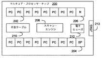
ここで図5を参照すると、データ処理システムが、複数の処理コア202を含むマルチコア・プロセッサ・チップ200を組み込んで示される。この図に示されるように、いくつかの処理コアは、例えばサービス・プロセッサ204といった、特殊目的用に指定することができ、いくつかの処理コアは、冗長なコア206と同様に未使用または予備であってよい。例えば、本発明の1つの実施形態では、実際に使用する16個の機能コアおよび1つのサービス・プロセッサ、ならびに1つの非活動状態の予備コアを有する意図で、マルチコア・プロセッサ・チップ200上に18個の処理コアを製造することが望ましい場合がある。次いで、BIST期間に、任意の処理コアが不良であると決定される場合、そのコアを非活動状態にして、予備コアを機能コアとして使用するために活動状態にすることができる。また、任意の機能コアが部分的に不良であると決定される場合、例えば、浮動小数点または他の補助機能ユニットが不良であると決定されるが、コアはサービス・プロセッサとして使用するのに場合によっては好適である場合、必要により、その部分的に不良のコアをサービス・プロセッサとして使用することができる。本発明の精神および範囲から逸脱することなく、異なる数の機能コア、予備コア、サービス・プロセッサなどを実装できることを理解されよう。 Referring now to FIG. 5, a data processing system is shown incorporating a multi-core processor chip 200 that includes a plurality of
本発明に一致する内部投票ベースのBISTを実装するために、マルチコア・プロセッサ・チップ200は、例えば、スキャン・エンジン208、不良テーブル210、および1つまたは複数の電子ヒューズ212を含む、スキャン論理部を含む。加えて、例えばJoint Test Automation Group(JTAG)標準を使用して実装される、従来型のテスト・ポート213を使用して、例えば外部の試験機器に、スキャン論理部への外部アクセスを可能にすることができる。 To implement an internal vote-based BIST consistent with the present invention, the multi-core processor chip 200 includes a scan logic unit that includes, for example, a
図6は、スキャン・エンジン208の一部の、1つの例示的な実装を示す。この実装では、スキャン・エンジン208は、3つのグループで処理コア202を試験するように構成され、したがって、3つの処理コア202A、202B、および202Cのそれぞれで、スキャン・チェイン214の入力および出力への接続が図で示されている。各スキャン・チェイン214は、典型的には、複数のラッチを含み、複数のラッチは、一緒にグループ化することができ、さもなければ、各処理コア内の複数の機能ユニット間で分散することができる。3つの処理コアを含むプロセッサ・チップに関し、図6では、そのチップについて内部投票ベースのBISTを実施するのに必要な比較論理部の全てを実装していることを理解されたい。4つ以上の処理コアを含むプロセッサ・チップに関し、図6に示されているスキャン・エンジン208の少なくとも一部が複製されて、3つの処理コアの他のグループを取り扱うことができる。別の場合には、4つ以上の処理コアの試験結果が比較されて、不良処理コアおよびその中の不良ラッチを識別することができる。 FIG. 6 illustrates one exemplary implementation of a portion of the
さらに、この実装では、スキャン・チェインは、単一のビット入力および単一のビット出力を有し、クロック・サイクル当たり1ビットの速度で、データが、スキャン・チェインにスキャン入力し、スキャン・チェインからスキャン出力することを可能にする、直列スキャン・チェインである。しかし、本発明は、本明細書に開示される特定のスキャン・チェイン実装に限定されないことを理解されよう。 In addition, in this implementation, the scan chain has a single bit input and a single bit output, and data is scanned into the scan chain at a rate of 1 bit per clock cycle. It is a serial scan chain that allows scanning out from However, it will be understood that the present invention is not limited to the particular scan chain implementation disclosed herein.
スキャン・エンジン208は、各処理コア202A〜Cのスキャン・チェイン214の入力に同じテスト・パターンを出力するために結合されるLFSR216および決定性テスト・パターン生成器218のうちの1つまたは両方を含むことができる。前者を使用して疑似乱数テスト・パターンを生成することができ、一方、後者を使用してテスト・パターンの決定性シーケンスを生成することができる。いくつかの実施形態では、LFSR216および決定性テスト・パターン生成器218のうちの1つだけが利用される。テスト・パターンの決定性シーケンスは、例えば、特定のプロセッサ・アーキテクチャ用に特に設計されたテスト・パターンを適用し、確実に設計物を効率的かつ完全に試験することに有用な場合がある。一方、疑似乱数試験は、本質的により力ずくな場合があるが、プロセッサ・チップで内部的に試験が起こり、任意の外部の試験機器に依拠しないので、試験を実施することができる速度は著しく速くなり、そのため、他の場合には外部の試験機器を介して適用される可能性があるものと同じ時間枠に著しく多数のテスト・パターンを適用することができ、そのため、疑似乱数テスト・パターンの使用を通して、多くのインスタンスで、十分な試験カバレッジを依然として得ることができることを理解されよう。単一のテスト・パターン生成器をプロセッサ・チップ内の全ての処理コアに適用できること、または異なるテスト・パターン生成器を処理コアの異なるグループに使用できることも理解されよう。
この実装では、不良テーブル210は、各処理コア用に、そのコアのスキャン・チェイン内の第1の不良ラッチの場所を記憶するデータ構造体として実装される。したがって、不良テーブル210は、それぞれ処理コア202A〜Cに関連付けられ、図6では、それぞれPCA、PCB、およびPCCと表される、少なくとも1つの記憶要素を含む。追加の処理コア用に追加の記憶要素をもうけることができ、いくつかの実施形態では、並列に試験される他のグループの処理コア用に不良テーブル210を複製することができること、または単一のデータ構造体を使用して、複数のグループの処理コア用に試験結果を記憶できることを理解されよう。 In this implementation, the failure table 210 is implemented for each processing core as a data structure that stores the location of the first failure latch in the scan chain of that core. Accordingly, the failure table 210 includes at least one storage element that is associated with each of the
スキャン・エンジン208は、処理コア202A〜C内のスキャン・チェインの単一ビット出力間の任意の不一致に応答して不一致信号224をアサートする、例えば1対のXNORゲート220、221およびNANDゲート222を含む比較論理部も含む。XNORゲート220は、処理コア202Aおよび202Bのスキャン・チェイン出力に排他的NOR演算を実施し、一方XNORゲート221は、処理コア202Bおよび202Cのスキャン・チェイン出力に排他的NOR演算を実施する。XNORゲート220、221の出力は、次いでNANDゲート222に送られ、処理コア202A〜Cにより出力されるビットの全てが一致しないときはいつでも、不一致信号224を不良テーブル210にアサートする。 The
比較論理部は、やはり処理コア202A〜Cの出力を受け取り、処理コアのうちのどれが、処理コアの大多数(ここでは、2個)により出力される「意見の一致」した正しいビットとは異なるビットを出力しているかを決定する、コアID論理部226も含む。コアID論理部226は、各処理コア202A〜C用に1つずつ、3つの選択信号を不良テーブル210に出力する。選択信号は、関連する処理コアが異常値である、すなわちそのビットに関しての不良処理コアであるときはいつでもアサートされる。加えて、カウンタ228を使用して、各スキャン・チェイン214内のビット位置に対応する、またはさもなければ相関する値を生成し、不良処理コアのスキャン・チェイン内のラッチに相関付けられる不一致ビットの位置決めを可能にする。カウンタ228の値は、やはり不良テーブル210に出力される。 The comparison logic also receives the output of the
任意の数Nの処理コア間の多数決を実装し、異常値処理コアを決定し、N個の処理コアから意見の一致する正しい結果を決定し、カウンタ値または他のラッチ/ビット位置識別器を管理する比較論理部を構成すること、ならびに複数のグループの処理ノードにわたるそのような論理部を複製することは、本開示の恩恵を被る当業者の能力の範囲内であろう。したがって、本発明は、本明細書に開示される特定の構成に限定されない。 Implement a majority vote between any number N of processing cores, determine outlier processing cores, determine a consensus correct result from N processing cores, counter values or other latch / bit position identifiers It would be within the ability of one of ordinary skill in the art to benefit from the present disclosure to configure the comparison logic to manage, and to replicate such logic across multiple groups of processing nodes. Accordingly, the present invention is not limited to the specific configurations disclosed herein.
不良テーブル210は、不一致信号224のアサートに応答して、コアID論理部226によりアサートされる関連するイネーブル信号により選択されるように、異常値処理コア202A〜Cに対応する記憶要素にカウンタ228の現在値を記憶するように構成される。この実装では、不良テーブル210は、各処理コア202A〜Cで検出された第1の不良ラッチに対応するカウンタ値を記憶し、図6に示されるように、処理コア202Aおよび202Cが不良であると識別され、一方処理コア202Bは不良と識別されない。 The failure table 210 is responsive to the assertion of the
カウンタ228がスキャン・チェイン内のラッチに相関付けられる方法は、異なる実施形態で変化することができる。例えば、図7は、命令または発行ユニット(IU)230、L1キャッシュ232、固定小数点実行ユニット(XU)234、および浮動小数点実行ユニット(FPU)236を含む、例示的な処理コア202を示す。この実装では、スキャン・チェイン214は、それぞれIU230、L1キャッシュ232、XU234、およびFPU236に配設される4つのラッチ・グループ238、240、242、および244に仕切られる。例えばマッピング・テーブル246といった、マッピング・データ構造体がスキャン・エンジンに組み込まれ、どの機能ユニットにスキャン・チェイン214内の特定のラッチまたはビット位置が配設されるのかをスキャン・エンジンが決定することを可能にすることができる。したがって、図7に示されるように、ラッチ/ビット位置1〜2000がIU230に対応することができ、ラッチ/ビット位置2001〜3000がL1キャッシュ232に対応することができ、ラッチ/ビット位置3001〜6000がXU234に対応することができ、ラッチ/ビット位置6001〜10000がFPU236に対応することができる。 The manner in which counter 228 is correlated to latches in the scan chain can vary in different embodiments. For example, FIG. 7 illustrates an
スキャン・チェイン214内のラッチ/ビット位置にカウンタ228(図6)を相関付けることにより、処理コア内の不良ラッチを検出すると、スキャン・エンジンがそのラッチ/ビット位置を処理コア202内の機能ユニットにマッピングし、そのことにより、処理コア内の不良機能ユニット(例えば、図6に一時的に戻ると、処理コア202AのIUおよび処理コア202CのL1キャッシュ)を識別することができる。さらに、いくつかの実施形態では、不良機能ユニットを知ることによって、スキャン・エンジンがその機能ユニットまたは処理コアを自動的にディセーブルにすることを可能にすることができ、またはさもなければ、不良機能ユニットに対処するため、プロセッサ・チップを自動的に再構成することを求めることができる。しかし、他の実施形態では、機能ユニットへのラッチ/ビット位置のマッピングは、外部の試験機器内に実装することができ、このことにより、ラッチ/ビット位置だけがオンボードでプロセッサ・チップに記憶され、不良機能ユニットの決定はオフチップで実施される。 When the counter 228 (FIG. 6) is correlated to the latch / bit position in the
図8は、本発明に一致する内部投票ベースのBISTを実施するための、マルチコア・プロセッサ・チップ200(図5)のスキャン・エンジン208により実施される例示的な動作のシーケンス250を示す。この実装では、全ての処理コアが同じテスト・パターンを受け取ることが仮定されている。したがって、ブロック252では、疑似乱数テスト・パターンまたは所定のテスト・パターンのいずれかのテスト・パターンが処理コアのうちの全てのスキャン・チェインにスキャン入力またはクロック入力される。次いで、処理コアは、N(1または複数)サイクルぶんクロック制御され(ブロック254)、入力されたテスト・パターンへの処理コアの応答を試験し、Nクロック・サイクル後に、クロックはブロック256で停止される。 FIG. 8 illustrates an exemplary sequence of
次いで、ブロック258で、ビット位置カウンタは、スキャン・チェインから出力される、第1のラッチまたはビット位置に対応する値にリセットされる。次いで、ブロック260で、処理コアのそれぞれのスキャン・チェインから試験結果がビット単位でクロック出力またはスキャン出力され、試験結果のビット単位比較を実施する。スキャン・チェインから出力されるビットの全てが互いに一致していれば、ブロック262は、ブロック264に制御を渡し、スキャン・チェインの次のラッチ/ビット位置に対応する値にカウンタを増加(または適切な場合は、減少)させる。ブロック266は、次いで、制御をブロック260に戻し、結果のスキャン出力を続ける。しかし、スキャン・エンジン内の比較論理部による試験結果ビット間の任意の不一致に応答して、ブロック262は制御をブロック268に渡し、例えば異常値処理コアに対応する記憶要素に現在のカウンタ値を記憶させることにより、不良テーブル内に不良を記憶する。次いで、制御がブロック264に渡り、カウンタを更新し、試験結果のスキャン出力を続ける。 Next, at
試験結果のビットの全てが一度スキャン出力されたら、ブロック266は制御をブロック270に渡し、適用されるべき追加のテスト・パターンが残っているかどうかを決定する。疑似乱数テスト・パターンについては、ブロック270は、所定の数のテスト・パターンの後に試験を停止することができる。テスト・パターンの所定のシーケンスについては、所望のシーケンス内のテスト・パターンの全てが一度適用されたら、ブロック270は、試験を停止することができる。したがって、追加のテスト・パターンを適用する必要がある場合、ブロック270は、制御をブロック252に戻し、新しいテスト・パターンでスキャンする。 Once all of the test result bits have been scanned out, block 266 passes control to block 270 to determine if additional test patterns remain to be applied. For pseudorandom test patterns, block 270 may stop testing after a predetermined number of test patterns. For a given sequence of test patterns, block 270 can stop the test once all of the test patterns in the desired sequence have been applied. Thus, if additional test patterns need to be applied, block 270 returns control to block 252 to scan with a new test pattern.
しかし、一度全てのテスト・パターンが適用されたら試験は完了し、ブロック270は、任意選択で制御をブロック272に渡し、チップをプログラムする。チップのプログラミングは、典型的には、自動的にチップの部分をディセーブルにすること、または外部の試験機器により取り出されて、チップの部分を後でディセーブルにするために、もしくは完全にチップを廃棄するために使用することができるデータを記憶することのいずれかを含む。 However, once all test patterns have been applied, the test is complete and block 270 optionally passes control to block 272 to program the chip. Chip programming typically disables a portion of the chip automatically, or is removed by an external test instrument to later disable the portion of the chip, or completely Including storing data that can be used to dispose of.
チップのプログラミングは、例えば、マッピング・テーブルにアクセスすること、および不良であると識別される処理コア内の任意の不良機能ユニットを自動的にディセーブルにすることを含むことができる。プログラミングは、処理コアを完全にディセーブルにすること、または別の処理コア(例えば、予備または冗長なコア)を再マッピングして元は不良処理コアに割り当てられた機能を取り扱うこと、あるいはその両方も含むことができる。プログラミングは、不良処理コアを選択して、例えばサービス・プロセッサとして機能するといった、特殊なタスクを取り扱うことも含むことができる。処理コア内の異なる機能ユニットで検出される不良に応じて、異なるアクションをとることができること、例えば、処理コアは、浮動小数点ユニットなしで低減した能力で依然として機能することができる場合があるが、発行ユニットなしでは完全に使用不可能な場合があることを理解されよう。 Chip programming can include, for example, accessing a mapping table and automatically disabling any defective functional units in the processing core that are identified as defective. Programming can either disable the processing core completely, or remap another processing core (eg, spare or redundant core) to handle the function originally assigned to the bad processing core, or both Can also be included. Programming can also include selecting a fault handling core to handle special tasks such as functioning as a service processor. Depending on the defects detected in different functional units within the processing core, different actions can be taken, for example, the processing core may still be able to function with reduced capacity without a floating point unit, It will be understood that it may not be completely usable without an issuing unit.
機能ユニットは、粒度の異なるレベルで規定できることも理解されよう。例えば、キャッシュまたは他のオンボード・メモリは、複数の機能ユニットに仕切ることができ、その結果、例えば、キャッシュの特定の部分が不良であると見い出された場合、キャッシュは、不良と識別されたキャッシュの部分に起因して、サイズが減少するが、依然として活動状態である。別の例として、実行ユニットの異なる部分が異なるタイプの命令を取り扱うことができ、実行ユニットの1つの部分内の不良によって、処理コアは、実行ユニットのその部分により取り扱われる任意の命令に関してソフトウェアをトラップして、その部分だけがディセーブルにされ、一方で、依然として他のタイプの命令を取り扱うためにイネーブルにされる結果となることができる。また、機能ユニットを階層的に規定することができ、特定の機能ユニットを他の機能ユニットが含むことができる。したがって、例えば、発行ユニット内の分岐予測ユニットが不良であると識別されるが、分岐予測ユニットをディセーブルにして依然として発行ユニットが動作することを可能にすることができる。 It will also be appreciated that functional units can be defined at different levels of granularity. For example, a cache or other on-board memory can be partitioned into multiple functional units so that, for example, if a particular portion of the cache is found to be bad, the cache has been identified as bad Due to the portion of the cache, it decreases in size but is still active. As another example, different parts of an execution unit can handle different types of instructions, and a defect in one part of the execution unit causes the processing core to run software for any instruction handled by that part of the execution unit. Trapping can result in only that portion being disabled, while still being enabled to handle other types of instructions. In addition, functional units can be defined hierarchically, and specific functional units can be included in other functional units. Thus, for example, a branch prediction unit in an issue unit can be identified as bad, but the branch prediction unit can be disabled to still allow the issue unit to operate.
チップをプログラムすることは、例えば、不良コード、または不良のラッチ、機能ユニットもしくは処理コアあるいはこれらの組合せの識別情報を記憶することにより、試験結果を不揮発性メモリに記憶することを含むこともできる。不揮発性メモリは、例えば、電子ヒューズとして、または当技術分野で知られている他の方法で実装することができる。 Programming the chip can also include storing test results in non-volatile memory, for example, by storing fault codes or faulty latches, functional units or processing cores or combinations thereof. . The non-volatile memory can be implemented, for example, as an electronic fuse or in other ways known in the art.
他のデータ構造体を使用して、本発明に一致する不良データを記憶できることも理解されよう。例えば、不良テーブルを電子ヒューズで実装することができ、そのため、各処理コア内の第1の不良ラッチだけが識別される。別の場合には、不良テーブルまたは他のデータ構造体が、特定の処理コアまたは機能ユニットあるいはその両方への、(所与の処理コア内で検出される複数の不良を含む)それぞれの検出された不良をマッピングする複数のエントリを記憶することができる。データ構造体は、カウンタ値ではなく機能ユニット識別子を記憶することもでき、または単に、もしも不良がある場合には、どの処理コアが不良であるのかを識別することができる。不良データ構造体は、イネーブル回路を兼ねることもでき、そのため、機能ユニットまたは処理コアあるいはその両方の不良のロギングによって、その特定のユニット/コアがイネーブルにされるかまたはディセーブルにされるかを示すその機能ユニットまたは処理コアあるいはその両方用のフラグを設定する結果となることができる。 It will also be appreciated that other data structures can be used to store bad data consistent with the present invention. For example, a failure table can be implemented with an electronic fuse so that only the first failure latch in each processing core is identified. In other cases, a defect table or other data structure is detected for each (including multiple defects detected within a given processing core) for a particular processing core and / or functional unit. Multiple entries can be stored that map the failure. The data structure can store a functional unit identifier rather than a counter value, or can simply identify which processing core is defective if there is a defect. A bad data structure can also serve as an enable circuit, so whether fault logging on a functional unit and / or processing core will enable or disable that particular unit / core. It can result in setting a flag for the functional unit and / or processing core shown.
したがって、本発明に一致する実施形態は、従来型の試験方法論を超えるいくつかの長所を提供する。プロセッサ・チップで内部にBISTを実装することにより、テスト・パターンまたは試験結果あるいはその両方がチップと外部の試験機器との間で通信されなければならない場合に可能であったよりも、著しく速く試験を実施することができる。多くの製造環境では、個別のプロセッサ・チップが外部の試験機器上に長く位置すると、それだけ、処理能力が低下して製造コストが大きくなり、この時間を減少すれば、処理能力を改善し、単位当たりのコストを低下させる。投票または比較論理部を実装することにより、所与のテスト・パターンについての「正しい」結果をシミュレートする必要、またはさもなければ前もって決定する必要がない。というのは、正しさは、処理コアの大多数がそれらのそれぞれの結果として何を出力するのかに単に基づいているからである。さらに、不良処理コアまたは不良機能ユニットあるいはその両方を識別することにより、不良処理コアまたは機能ユニットあるいはその両方を含む多くのチップは、その全体が廃棄されるのではなく、依然として低減した能力で動作するように再構成することができる。 Accordingly, embodiments consistent with the present invention provide several advantages over conventional test methodologies. By implementing BIST internally on the processor chip, tests can be performed significantly faster than was possible if test patterns and / or test results had to be communicated between the chip and external test equipment. Can be implemented. In many manufacturing environments, the longer the individual processor chips are located on external test equipment, the lower the processing power and the higher the manufacturing cost. Reduce the cost per hit. By implementing voting or comparison logic, a “correct” result for a given test pattern need not be simulated or otherwise determined in advance. This is because correctness is simply based on what the majority of processing cores output as their respective result. In addition, by identifying the fault handling core and / or functional unit, many chips that contain the fault handling core and / or functional unit still operate with reduced capacity rather than being discarded in their entirety. Can be reconfigured to
本発明の精神および範囲から逸脱することなく、開示された実施形態に対し、様々な変更を行うことができる。したがって、本発明は、添付される特許請求の範囲に存在する。 Various changes can be made to the disclosed embodiments without departing from the spirit and scope of the invention. Accordingly, the present invention resides in the claims hereinafter appended.
Claims (25)
Translated fromJapanese前記マルチコア集積回路デバイス上に配設され、前記複数の処理コアの前記スキャン・チェインにテスト・パターンを通信し、前記テスト・パターンに応じて前記複数の処理コアの前記スキャン・チェインにより出力される試験結果を比較するように構成される、スキャン論理部であって、前記複数の処理コアにより出力される前記試験結果の大多数と異なる不良処理コアの前記スキャン・チェインにより出力される前記試験結果に基づいて、前記複数の処理コアのうちの前記不良処理コアを識別するようにさらに構成される、前記スキャン論理部と
を備える、回路装置。A plurality of processing cores disposed on a multi-core integrated circuit device, each processing core including a scan chain; and
A test pattern is disposed on the multi-core integrated circuit device, communicates a test pattern to the scan chain of the plurality of processing cores, and is output by the scan chain of the plurality of processing cores according to the test pattern A scan logic configured to compare test results, wherein the test results output by the scan chain of the faulty processing cores differ from the majority of the test results output by the plurality of processing cores. And the scan logic unit further configured to identify the defective processing core of the plurality of processing cores.
前記テスト・パターンを前記複数の処理コアの前記スキャン・チェインにクロック入力し、
前記複数の処理コアを複数のクロック・サイクルの間クロック制御し、
前記複数の処理コアの前記スキャン・チェインから前記試験結果をクロック出力する
ように構成される、請求項3に記載の回路装置。The scan logic is configured to communicate a plurality of test patterns to the plurality of processing cores, for each test pattern;
Clocking the test pattern into the scan chain of the plurality of processing cores;
Clocking the plurality of processing cores for a plurality of clock cycles;
4. The circuit device according to claim 3, wherein the circuit device is configured to clock out the test result from the scan chain of the plurality of processing cores.
前記マルチコア集積回路デバイス上に配設されたスキャン論理部を使用して、前記複数の処理コアの前記スキャン・チェインにテスト・パターンを通信するステップと、
前記スキャン論理部を使用して前記テスト・パターンに応じて前記複数の処理コアの前記スキャン・チェインにより出力される試験結果を比較するステップと、
前記複数の処理コアにより出力される前記試験結果の大多数と異なる前記不良処理コアの前記スキャン・チェインにより出力される前記試験結果に基づいて、前記複数の処理コアのうちの不良処理コアを識別するステップと
を含む方法。A method for performing a built-in self test (BIST) of a multi-core integrated circuit device including a plurality of processing cores, each processing core including a scan chain,
Communicating test patterns to the scan chains of the plurality of processing cores using scan logic disposed on the multi-core integrated circuit device;
Comparing the test results output by the scan chains of the plurality of processing cores according to the test pattern using the scan logic;
Identifying defective processing cores of the plurality of processing cores based on the test results output by the scan chain of the defective processing cores different from the majority of the test results output by the plurality of processing cores Comprising the steps of:
Applications Claiming Priority (3)
| Application Number | Priority Date | Filing Date | Title |
|---|---|---|---|
| US13/330,921 | 2011-12-20 | ||
| US13/330,921US8856602B2 (en) | 2011-12-20 | 2011-12-20 | Multi-core processor with internal voting-based built in self test (BIST) |
| PCT/CN2012/084175WO2013091446A1 (en) | 2011-12-20 | 2012-11-07 | Multi-core processor with internal voting-based built in self test (bist) |
Publications (1)
| Publication Number | Publication Date |
|---|---|
| JP2015509183Atrue JP2015509183A (en) | 2015-03-26 |
Family
ID=48611507
Family Applications (1)
| Application Number | Title | Priority Date | Filing Date |
|---|---|---|---|
| JP2014547684APendingJP2015509183A (en) | 2011-12-20 | 2012-11-07 | CIRCUIT DEVICE, INTEGRATED CIRCUIT DEVICE, PROGRAM PRODUCT, AND METHOD (Multi-core processor with internal voting based built-in self test (BIST)) |
Country Status (6)
| Country | Link |
|---|---|
| US (1) | US8856602B2 (en) |
| JP (1) | JP2015509183A (en) |
| CN (1) | CN104040499B (en) |
| DE (1) | DE112012005320T5 (en) |
| GB (1) | GB2511972B (en) |
| WO (1) | WO2013091446A1 (en) |
Cited By (12)
| Publication number | Priority date | Publication date | Assignee | Title |
|---|---|---|---|---|
| CN111078625A (en)* | 2018-10-18 | 2020-04-28 | 上海寒武纪信息科技有限公司 | Network-on-chip processing system and network-on-chip data processing method |
| CN111078624A (en)* | 2018-10-18 | 2020-04-28 | 上海寒武纪信息科技有限公司 | Network-on-chip processing system and network-on-chip data processing method |
| CN111078623A (en)* | 2018-10-18 | 2020-04-28 | 上海寒武纪信息科技有限公司 | On-chip network processing system and on-chip network data processing method |
| JP2020204913A (en)* | 2019-06-17 | 2020-12-24 | 富士通株式会社 | Arithmetic processing device and information processing device |
| KR20210020927A (en)* | 2018-06-27 | 2021-02-24 | 상하이 캠브리콘 인포메이션 테크놀로지 컴퍼니 리미티드 | On-chip code breakpoint debug method, on-chip processor and chip debug system with breakpoint |
| JP2021038976A (en)* | 2019-09-02 | 2021-03-11 | 株式会社東芝 | Semiconductor integrated circuit and its test method |
| JP2021526277A (en)* | 2018-10-18 | 2021-09-30 | シャンハイ カンブリコン インフォメーション テクノロジー カンパニー リミテッドShanghai Cambricon Information Technology Co.,Ltd. | Network-on-chip data processing methods and equipment |
| KR20230002740A (en)* | 2020-05-14 | 2023-01-05 | 노스롭 그루먼 시스템즈 코포레이션 | Testing and characterization of rings in the superconducting region with built-in self-tests |
| US12093148B2 (en) | 2019-06-12 | 2024-09-17 | Shanghai Cambricon Information Technology Co., Ltd | Neural network quantization parameter determination method and related products |
| US12112257B2 (en) | 2019-08-27 | 2024-10-08 | Anhui Cambricon Information Technology Co., Ltd. | Data processing method, device, computer equipment and storage medium |
| US12165039B2 (en) | 2019-08-23 | 2024-12-10 | Anhui Cambricon Information Technology Co., Ltd. | Neural network quantization data processing method, device, computer equipment and storage medium |
| US12333671B2 (en) | 2020-02-24 | 2025-06-17 | Cambricon Technologies Corporation Limited | Data quantization processing method and apparatus, electronic device and storage medium |
Families Citing this family (45)
| Publication number | Priority date | Publication date | Assignee | Title |
|---|---|---|---|---|
| JP5900061B2 (en)* | 2012-03-19 | 2016-04-06 | 富士通株式会社 | Test method, test apparatus and program |
| JP6074955B2 (en)* | 2012-08-31 | 2017-02-08 | 富士通株式会社 | Information processing apparatus and control method |
| JP5818762B2 (en)* | 2012-09-14 | 2015-11-18 | 株式会社東芝 | Programmable logic device and verification method thereof |
| KR101457557B1 (en)* | 2013-01-18 | 2014-11-04 | 연세대학교 산학협력단 | Multi-core device, test device and method for diagnosing failure |
| US9720041B2 (en)* | 2013-02-01 | 2017-08-01 | Mentor Graphics Corporation | Scan-based test architecture for interconnects in stacked designs |
| JP6282482B2 (en)* | 2014-02-18 | 2018-02-21 | 株式会社日立製作所 | Programmable circuit device and configuration information restoration method |
| US9244124B2 (en)* | 2014-03-28 | 2016-01-26 | International Business Machines Corporation | Initializing and testing integrated circuits with selectable scan chains with exclusive-or outputs |
| CN105629148B (en)* | 2014-10-28 | 2018-08-28 | 国际商业机器公司 | The test method and test equipment of multiple modules in test circuit |
| JP6491507B2 (en)* | 2015-03-20 | 2019-03-27 | ルネサスエレクトロニクス株式会社 | Semiconductor device, electronic device and self-diagnosis method of semiconductor device |
| CN106680688B (en) | 2015-11-11 | 2020-09-25 | 恩智浦美国有限公司 | Testing multi-core integrated circuits using parallel scan test data input and output |
| US10395751B2 (en)* | 2016-06-28 | 2019-08-27 | SK Hynix Inc. | Automated testing system and operating method thereof |
| CN106991022B (en)* | 2017-03-07 | 2020-12-18 | 记忆科技(深圳)有限公司 | Chip analysis method based on scan chain |
| US10635526B2 (en)* | 2017-06-12 | 2020-04-28 | Sandisk Technologies Llc | Multicore on-die memory microcontroller |
| CN107544017B (en)* | 2017-07-12 | 2020-06-16 | 清华大学 | A low-power weighted pseudo-random test method and related equipment based on vector compression |
| US10831626B2 (en) | 2017-10-19 | 2020-11-10 | International Business Machines Corporation | Method to sort partially good cores for specific operating system usage |
| US10628274B2 (en)* | 2017-12-05 | 2020-04-21 | Qualcomm Incorporated | Self-test during idle cycles for shader core of GPU |
| CN108600040B (en)* | 2018-03-16 | 2022-03-15 | 国电南瑞科技股份有限公司 | A node fault detection method for distributed systems based on high availability detection nodes |
| US10740523B1 (en)* | 2018-07-12 | 2020-08-11 | Xilinx, Inc. | Systems and methods for providing defect recovery in an integrated circuit |
| US11645178B2 (en)* | 2018-07-27 | 2023-05-09 | MIPS Tech, LLC | Fail-safe semi-autonomous or autonomous vehicle processor array redundancy which permits an agent to perform a function based on comparing valid output from sets of redundant processors |
| TWI803695B (en) | 2018-11-07 | 2023-06-01 | 日商索尼半導體解決方案公司 | Camera and Electronic Equipment |
| US11074147B2 (en) | 2018-11-30 | 2021-07-27 | International Business Machines Corporation | Continuous mutual extended processor self-test |
| US10866280B2 (en)* | 2019-04-01 | 2020-12-15 | Texas Instruments Incorporated | Scan chain self-testing of lockstep cores on reset |
| CN112148536B (en)* | 2019-06-26 | 2025-07-04 | 昆仑芯(北京)科技有限公司 | Method, device, electronic device and computer storage medium for detecting deep learning chip |
| US10998075B2 (en)* | 2019-09-11 | 2021-05-04 | International Business Machines Corporation | Built-in self-test for bit-write enabled memory arrays |
| US10971242B2 (en) | 2019-09-11 | 2021-04-06 | International Business Machines Corporation | Sequential error capture during memory test |
| US12111356B2 (en) | 2019-10-11 | 2024-10-08 | Erik Larsson | System and method for access control of a plurality of instruments embedded in a semiconductor device |
| US11181579B2 (en)* | 2019-10-21 | 2021-11-23 | Advanced Micro Devices, Inc. | Performing scan data transfer inside multi-die package with SERDES functionality |
| CN110673021B (en)* | 2019-11-05 | 2021-09-10 | 桂林电子科技大学 | NoC-based boundary scan test control method and controller interface |
| CN111308329B (en)* | 2020-03-20 | 2022-02-25 | 深圳芯行科技有限公司 | Circuit, device and method for testability design of many-core computing chip |
| US11244741B1 (en)* | 2020-11-04 | 2022-02-08 | Micron Technology, Inc. | Selectable fuse sets, and related methods, devices, and systems |
| CN112630630B (en)* | 2020-11-30 | 2022-10-28 | 深圳比特微电子科技有限公司 | Chip testing method and computing chip |
| CN114460447B (en)* | 2021-01-19 | 2023-03-28 | 沐曦集成电路(上海)有限公司 | Self-test circuit and self-test method of latch |
| US20220237353A1 (en)* | 2021-01-27 | 2022-07-28 | Taiwan Semiconductor Manufacturing Company Limited | Fault detection of circuit based on virtual defects |
| CN113010354B (en)* | 2021-03-22 | 2024-11-01 | 北京灵汐科技有限公司 | Nuclear classification method, mapping method, data transmission method and device and chip |
| WO2022199390A1 (en)* | 2021-03-22 | 2022-09-29 | 北京灵汐科技有限公司 | Processing method and apparatus, electronic device, and storage medium |
| TWI760157B (en)* | 2021-03-24 | 2022-04-01 | 德律科技股份有限公司 | System and method of testing a single dut through multiple cores in parallel |
| US12332309B2 (en)* | 2021-08-11 | 2025-06-17 | Intel Corporation | Built-in self-test for network on chip fabric |
| US20230085994A1 (en)* | 2021-09-17 | 2023-03-23 | Intel Corporation | Logical resource partitioning via realm isolation |
| CN115201669B (en)* | 2022-09-16 | 2022-11-15 | 中诚华隆计算机技术有限公司 | Chip internal circuit detection method and device |
| US20240160825A1 (en)* | 2022-11-10 | 2024-05-16 | Cornami, Inc. | Method and system for providing fault tolerant layout of massively parallel processing array |
| CN116755953B (en)* | 2023-08-22 | 2023-12-19 | 北京象帝先计算技术有限公司 | Test result grouping method, device, electronic equipment and readable storage medium |
| GB2634300A (en)* | 2023-10-06 | 2025-04-09 | Imagination Tech Ltd | Processing instructions at a processing unit configured to perform parallel processing |
| CN119782140A (en)* | 2023-10-06 | 2025-04-08 | 想象技术有限公司 | Processing units configured to perform parallel processing |
| GB2634299A (en)* | 2023-10-06 | 2025-04-09 | Imagination Tech Ltd | Processing unit configured to perform parallel processing |
| US20250265162A1 (en)* | 2024-02-21 | 2025-08-21 | Google Llc | Instances For Built-In Self Testing |
Family Cites Families (15)
| Publication number | Priority date | Publication date | Assignee | Title |
|---|---|---|---|---|
| US5732209A (en)* | 1995-11-29 | 1998-03-24 | Exponential Technology, Inc. | Self-testing multi-processor die with internal compare points |
| US6671839B1 (en)* | 2002-06-27 | 2003-12-30 | Logicvision, Inc. | Scan test method for providing real time identification of failing test patterns and test bist controller for use therewith |
| US7424658B1 (en)* | 2002-07-01 | 2008-09-09 | Altera Corporation | Method and apparatus for testing integrated circuits |
| US7509600B2 (en)* | 2004-04-22 | 2009-03-24 | Janusz Rajski | Generating test patterns having enhanced coverage of untargeted defects |
| US7263642B1 (en) | 2005-09-15 | 2007-08-28 | Azul Systems, Inc | Testing replicated sub-systems in a yield-enhancing chip-test environment using on-chip compare to expected results for parallel scan chains testing critical and repairable sections of each sub-system |
| TW200801550A (en)* | 2006-01-06 | 2008-01-01 | Koninkl Philips Electronics Nv | IC testing methods and apparatus |
| US20070300115A1 (en)* | 2006-06-01 | 2007-12-27 | Ramyanshu Datta | Apparatus and method for accelerating test, debug and failure analysis of a multiprocessor device |
| US8030649B2 (en)* | 2006-07-28 | 2011-10-04 | International Business Machines Corporation | Scan testing in single-chip multicore systems |
| JP4815326B2 (en)* | 2006-10-31 | 2011-11-16 | 富士通株式会社 | Integrated circuit timing failure improvement apparatus, integrated circuit timing failure diagnosis apparatus and method, and integrated circuit |
| DE102006059158B4 (en)* | 2006-12-14 | 2009-06-10 | Advanced Micro Devices, Inc., Sunnyvale | Integrated circuit chip with at least two circuit cores and associated method for testing |
| DE102006059156B4 (en)* | 2006-12-14 | 2008-11-06 | Advanced Micro Devices, Inc., Sunnyvale | Method for testing an integrated circuit chip with at least two circuit cores and integrated circuit chip and test system |
| US7657805B2 (en)* | 2007-07-02 | 2010-02-02 | Sun Microsystems, Inc. | Integrated circuit with blocking pin to coordinate entry into test mode |
| US20090089636A1 (en)* | 2007-10-01 | 2009-04-02 | Fernsler Matthew E | Method and Apparatus for Logic Built In Self Test (LBIST) Fault Detection in Multi-Core Processors |
| JP5201151B2 (en)* | 2008-01-10 | 2013-06-05 | 富士通株式会社 | Test pattern generation method, apparatus and program |
| TW201005311A (en)* | 2008-07-23 | 2010-02-01 | Ind Tech Res Inst | Test device and method for an SoC test architecture |
- 2011
- 2011-12-20USUS13/330,921patent/US8856602B2/enactiveActive
- 2012
- 2012-11-07GBGB1410749.4Apatent/GB2511972B/enactiveActive
- 2012-11-07CNCN201280063683.4Apatent/CN104040499B/enactiveActive
- 2012-11-07DEDE112012005320.6Tpatent/DE112012005320T5/enactivePending
- 2012-11-07JPJP2014547684Apatent/JP2015509183A/enactivePending
- 2012-11-07WOPCT/CN2012/084175patent/WO2013091446A1/enactiveApplication Filing
Cited By (36)
| Publication number | Priority date | Publication date | Assignee | Title |
|---|---|---|---|---|
| JP2021520566A (en)* | 2018-06-27 | 2021-08-19 | シャンハイ カンブリコン インフォメーション テクノロジー カンパニー リミテッドShanghai Cambricon Information Technology Co.,Ltd. | On-chip code breakpoint debugging method, on-chip processor and breakpoint-based chip debugging system |
| US11789847B2 (en) | 2018-06-27 | 2023-10-17 | Shanghai Cambricon Information Technology Co., Ltd | On-chip code breakpoint debugging method, on-chip processor, and chip breakpoint debugging system |
| KR102470893B1 (en)* | 2018-06-27 | 2022-11-25 | 상하이 캠브리콘 인포메이션 테크놀로지 컴퍼니 리미티드 | Debug method by breakpoint of on-chip code, chip debug system by on-chip processor and breakpoint |
| JP7053891B2 (en) | 2018-06-27 | 2022-04-12 | シャンハイ カンブリコン インフォメーション テクノロジー カンパニー リミテッド | On-chip code breakpoint debugging method, on-chip processor and breakpoint-based chip debugging system |
| KR20210020927A (en)* | 2018-06-27 | 2021-02-24 | 상하이 캠브리콘 인포메이션 테크놀로지 컴퍼니 리미티드 | On-chip code breakpoint debug method, on-chip processor and chip debug system with breakpoint |
| JP7053775B2 (en) | 2018-10-18 | 2022-04-12 | シャンハイ カンブリコン インフォメーション テクノロジー カンパニー リミテッド | Network-on-chip data processing methods and equipment |
| CN111078623A (en)* | 2018-10-18 | 2020-04-28 | 上海寒武纪信息科技有限公司 | On-chip network processing system and on-chip network data processing method |
| JP2021526277A (en)* | 2018-10-18 | 2021-09-30 | シャンハイ カンブリコン インフォメーション テクノロジー カンパニー リミテッドShanghai Cambricon Information Technology Co.,Ltd. | Network-on-chip data processing methods and equipment |
| JP2021166032A (en)* | 2018-10-18 | 2021-10-14 | シャンハイ カンブリコン インフォメーション テクノロジー カンパニー リミテッドShanghai Cambricon Information Technology Co., Ltd. | Network-on-chip data processing method and device |
| US12061564B2 (en) | 2018-10-18 | 2024-08-13 | Shanghai Cambricon Information Technology Co., Ltd. | Network-on-chip data processing based on operation field and opcode |
| CN111078623B (en)* | 2018-10-18 | 2022-03-29 | 上海寒武纪信息科技有限公司 | Network-on-chip processing system and network-on-chip data processing method |
| CN111078625B (en)* | 2018-10-18 | 2022-03-29 | 上海寒武纪信息科技有限公司 | Network-on-chip processing system and network-on-chip data processing method |
| US11880328B2 (en) | 2018-10-18 | 2024-01-23 | Shanghai Cambricon Information Technology Co., Ltd. | Network-on-chip data processing method and device |
| US12204479B2 (en) | 2018-10-18 | 2025-01-21 | Shanghai Cambricon Information Technology Co., Ltd. | Network-on-chip data processing method and device |
| JP7060720B2 (en) | 2018-10-18 | 2022-04-26 | シャンハイ カンブリコン インフォメーション テクノロジー カンパニー リミテッド | Network-on-chip data processing methods and equipment |
| US11971836B2 (en) | 2018-10-18 | 2024-04-30 | Shanghai Cambricon Information Technology Co., Ltd. | Network-on-chip data processing method and device |
| US11880329B2 (en) | 2018-10-18 | 2024-01-23 | Shanghai Cambricon Information Technology Co., Ltd. | Arbitration based machine learning data processor |
| US11960431B2 (en) | 2018-10-18 | 2024-04-16 | Guangzhou University | Network-on-chip data processing method and device |
| CN111078625A (en)* | 2018-10-18 | 2020-04-28 | 上海寒武纪信息科技有限公司 | Network-on-chip processing system and network-on-chip data processing method |
| CN111078624A (en)* | 2018-10-18 | 2020-04-28 | 上海寒武纪信息科技有限公司 | Network-on-chip processing system and network-on-chip data processing method |
| US11797467B2 (en) | 2018-10-18 | 2023-10-24 | Shanghai Cambricon Information Technology Co., Ltd. | Data processing device with transmission circuit |
| US11809360B2 (en) | 2018-10-18 | 2023-11-07 | Shanghai Cambricon Information Technology Co., Ltd. | Network-on-chip data processing method and device |
| US11841816B2 (en) | 2018-10-18 | 2023-12-12 | Shanghai Cambricon Information Technology Co., Ltd. | Network-on-chip data processing method and device |
| US11868299B2 (en) | 2018-10-18 | 2024-01-09 | Shanghai Cambricon Information Technology Co., Ltd. | Network-on-chip data processing method and device |
| US11880330B2 (en) | 2018-10-18 | 2024-01-23 | Shanghai Cambricon Information Technology Co., Ltd. | Network-on-chip data processing method and device |
| US12093148B2 (en) | 2019-06-12 | 2024-09-17 | Shanghai Cambricon Information Technology Co., Ltd | Neural network quantization parameter determination method and related products |
| JP7331482B2 (en) | 2019-06-17 | 2023-08-23 | 富士通株式会社 | Arithmetic processing device and information processing device |
| JP2020204913A (en)* | 2019-06-17 | 2020-12-24 | 富士通株式会社 | Arithmetic processing device and information processing device |
| US12165039B2 (en) | 2019-08-23 | 2024-12-10 | Anhui Cambricon Information Technology Co., Ltd. | Neural network quantization data processing method, device, computer equipment and storage medium |
| US12112257B2 (en) | 2019-08-27 | 2024-10-08 | Anhui Cambricon Information Technology Co., Ltd. | Data processing method, device, computer equipment and storage medium |
| JP7150676B2 (en) | 2019-09-02 | 2022-10-11 | 株式会社東芝 | Semiconductor integrated circuit and its test method |
| US11280831B2 (en) | 2019-09-02 | 2022-03-22 | Kabushiki Kaisha Toshiba | Semiconductor integrated circuit with self testing and method of testing |
| JP2021038976A (en)* | 2019-09-02 | 2021-03-11 | 株式会社東芝 | Semiconductor integrated circuit and its test method |
| US12333671B2 (en) | 2020-02-24 | 2025-06-17 | Cambricon Technologies Corporation Limited | Data quantization processing method and apparatus, electronic device and storage medium |
| KR20230002740A (en)* | 2020-05-14 | 2023-01-05 | 노스롭 그루먼 시스템즈 코포레이션 | Testing and characterization of rings in the superconducting region with built-in self-tests |
| KR102791442B1 (en) | 2020-05-14 | 2025-04-08 | 노스롭 그루먼 시스템즈 코포레이션 | Testing and characterization of rings in the superconducting region using built-in self-test |
Also Published As
| Publication number | Publication date |
|---|---|
| CN104040499B (en) | 2017-09-12 |
| US8856602B2 (en) | 2014-10-07 |
| GB2511972A (en) | 2014-09-17 |
| US20130159799A1 (en) | 2013-06-20 |
| CN104040499A (en) | 2014-09-10 |
| DE112012005320T5 (en) | 2014-10-02 |
| GB201410749D0 (en) | 2014-07-30 |
| WO2013091446A1 (en) | 2013-06-27 |
| GB2511972B (en) | 2017-09-20 |
Similar Documents
| Publication | Publication Date | Title |
|---|---|---|
| US8856602B2 (en) | Multi-core processor with internal voting-based built in self test (BIST) | |
| US20220164284A1 (en) | In-memory zero value detection | |
| US9026423B2 (en) | Fault support in an emulation environment | |
| US7756695B2 (en) | Accelerated simulation and verification of a system under test (SUT) using cache and replacement management tables | |
| US20100042813A1 (en) | Redundant Execution of Instructions in Multistage Execution Pipeline During Unused Execution Cycles | |
| Bayraktaroglu et al. | Cache resident functional microprocessor testing: Avoiding high speed io issues | |
| US8626965B2 (en) | Using a DMA engine to automatically validate DMA data paths | |
| Lnu | AI-Driven Verification for Compute Express Link (CXL): Challenges, Innovations, and Future | |
| US11105854B2 (en) | System, apparatus and method for inter-die functional testing of an integrated circuit | |
| Bhowmik et al. | A low-cost test solution for reliable communication in networks-on-chip | |
| US20070195716A1 (en) | Ring bus in an emulation environment | |
| US9864830B1 (en) | Method and apparatus for placement and routing of circuit designs | |
| US10410713B1 (en) | Content addressable memory modeling in emulation and prototyping | |
| Ku et al. | Testing reliability techniques for SoCs with fault tolerant CGRA by using live FPGA fault injection | |
| US12001362B2 (en) | Dynamically reprogrammable topologically unique integrated circuit identification | |
| Carretero et al. | Hardware/software-based diagnosis of load-store queues using expandable activity logs | |
| Neishaburi et al. | An infrastructure for debug using clusters of assertion-checkers | |
| US10043027B1 (en) | Generation of mask-value pairs for managing access to memory segments | |
| Li et al. | Fault tolerance on-chip: a reliable computing paradigm using self-test, self-diagnosis, and self-repair (3S) approach | |
| Janac | Network‐on‐Chip (NoC): The Technology that Enabled Multi‐processor Systems‐on‐Chip (MPSoCs) | |
| Strano et al. | Exploiting structural redundancy of SIMD accelerators for their built-in self-testing/diagnosis and reconfiguration | |
| US20240338289A1 (en) | Method of performance harvesting in core matrix structure and device of performing the same | |
| Ganeshpure et al. | A DFT Methodology for Repairing Embedded Memories of Large MPSoCs | |
| Malik | Evaluation of isolation design flow (IDF) for Single Chip Cryptography (SCC) application | |
| Crupi | Specification and Implementation of a Dependable SoC Platform Based on the RISC-V Instruction Set Architecture |