JP2015508574A - Steam treatment process for pattern smoothing and slimming of inline critical dimensions - Google Patents
Steam treatment process for pattern smoothing and slimming of inline critical dimensionsDownload PDFInfo
- Publication number
- JP2015508574A JP2015508574AJP2014551251AJP2014551251AJP2015508574AJP 2015508574 AJP2015508574 AJP 2015508574AJP 2014551251 AJP2014551251 AJP 2014551251AJP 2014551251 AJP2014551251 AJP 2014551251AJP 2015508574 AJP2015508574 AJP 2015508574A
- Authority
- JP
- Japan
- Prior art keywords
- pattern
- roughness
- sensitive material
- radiation sensitive
- substrate
- Prior art date
- Legal status (The legal status is an assumption and is not a legal conclusion. Google has not performed a legal analysis and makes no representation as to the accuracy of the status listed.)
- Granted
Links
- 238000000034methodMethods0.000titleclaimsabstractdescription356
- 230000008569processEffects0.000titleclaimsabstractdescription278
- 238000009499grossingMethods0.000titleclaimsabstractdescription87
- 239000000463materialSubstances0.000claimsabstractdescription220
- 230000005855radiationEffects0.000claimsabstractdescription197
- 239000000758substrateSubstances0.000claimsabstractdescription118
- 238000000059patterningMethods0.000claimsabstractdescription33
- 238000001459lithographyMethods0.000claimsdescription24
- 230000009467reductionEffects0.000claimsdescription20
- 238000012545processingMethods0.000claimsdescription11
- 238000010438heat treatmentMethods0.000claimsdescription10
- 239000002253acidSubstances0.000claimsdescription7
- 238000010894electron beam technologyMethods0.000claimsdescription7
- SECXISVLQFMRJM-UHFFFAOYSA-NN-MethylpyrrolidoneChemical compoundCN1CCCC1=OSECXISVLQFMRJM-UHFFFAOYSA-N0.000claimsdescription6
- 150000001875compoundsChemical class0.000claimsdescription4
- 238000012546transferMethods0.000claimsdescription3
- 230000001678irradiating effectEffects0.000claims2
- 239000010410layerSubstances0.000description152
- 239000000243solutionSubstances0.000description86
- WGTYBPLFGIVFAS-UHFFFAOYSA-Mtetramethylammonium hydroxideChemical compound[OH-].C[N+](C)(C)CWGTYBPLFGIVFAS-UHFFFAOYSA-M0.000description52
- 238000011161developmentMethods0.000description39
- 229920002120photoresistant polymerPolymers0.000description22
- 238000000576coating methodMethods0.000description21
- 239000011248coating agentSubstances0.000description14
- 238000000206photolithographyMethods0.000description14
- 238000001816coolingMethods0.000description13
- 238000005530etchingMethods0.000description13
- 101100215341Arabidopsis thaliana ACT12 geneProteins0.000description12
- 101100434207Arabidopsis thaliana ACT8 geneProteins0.000description12
- 238000001020plasma etchingMethods0.000description10
- 239000007789gasSubstances0.000description9
- 239000012071phaseSubstances0.000description9
- 238000001312dry etchingMethods0.000description8
- 238000004528spin coatingMethods0.000description8
- 238000000151depositionMethods0.000description7
- 238000001035dryingMethods0.000description7
- 239000010408filmSubstances0.000description7
- 239000010409thin filmSubstances0.000description7
- KFZMGEQAYNKOFK-UHFFFAOYSA-NIsopropanolChemical compoundCC(C)OKFZMGEQAYNKOFK-UHFFFAOYSA-N0.000description6
- 238000004132cross linkingMethods0.000description5
- 238000000609electron-beam lithographyMethods0.000description5
- 230000008859changeEffects0.000description4
- 238000002360preparation methodMethods0.000description4
- 239000011241protective layerSubstances0.000description4
- 239000000126substanceSubstances0.000description4
- 238000001039wet etchingMethods0.000description4
- 238000000231atomic layer depositionMethods0.000description3
- 230000006378damageEffects0.000description3
- 230000007547defectEffects0.000description3
- 239000012530fluidSubstances0.000description3
- 239000007788liquidSubstances0.000description3
- 229920001187thermosetting polymerPolymers0.000description3
- 239000012670alkaline solutionSubstances0.000description2
- 239000000908ammonium hydroxideSubstances0.000description2
- 239000003795chemical substances by applicationSubstances0.000description2
- 238000005229chemical vapour depositionMethods0.000description2
- 238000004140cleaningMethods0.000description2
- XLYOFNOQVPJJNP-UHFFFAOYSA-MhydroxideChemical compound[OH-]XLYOFNOQVPJJNP-UHFFFAOYSA-M0.000description2
- 239000007791liquid phaseSubstances0.000description2
- 125000001453quaternary ammonium groupChemical group0.000description2
- 230000000717retained effectEffects0.000description2
- 239000004065semiconductorSubstances0.000description2
- LIVNPJMFVYWSIS-UHFFFAOYSA-Nsilicon monoxideChemical compound[Si-]#[O+]LIVNPJMFVYWSIS-UHFFFAOYSA-N0.000description2
- 239000002344surface layerSubstances0.000description2
- 239000004094surface-active agentSubstances0.000description2
- 229910052581Si3N4Inorganic materials0.000description1
- VYPSYNLAJGMNEJ-UHFFFAOYSA-NSilicium dioxideChemical compoundO=[Si]=OVYPSYNLAJGMNEJ-UHFFFAOYSA-N0.000description1
- XUIMIQQOPSSXEZ-UHFFFAOYSA-NSiliconChemical compound[Si]XUIMIQQOPSSXEZ-UHFFFAOYSA-N0.000description1
- 230000002378acidificating effectEffects0.000description1
- QVGXLLKOCUKJST-UHFFFAOYSA-Natomic oxygenChemical compound[O]QVGXLLKOCUKJST-UHFFFAOYSA-N0.000description1
- 230000008021depositionEffects0.000description1
- 238000005137deposition processMethods0.000description1
- 230000006872improvementEffects0.000description1
- 238000002844meltingMethods0.000description1
- 230000008018meltingEffects0.000description1
- 238000012986modificationMethods0.000description1
- 230000004048modificationEffects0.000description1
- 150000004767nitridesChemical class0.000description1
- 229910052760oxygenInorganic materials0.000description1
- 239000001301oxygenSubstances0.000description1
- 238000005268plasma chemical vapour depositionMethods0.000description1
- 238000003672processing methodMethods0.000description1
- 229910052710siliconInorganic materials0.000description1
- 239000010703siliconSubstances0.000description1
- HQVNEWCFYHHQES-UHFFFAOYSA-Nsilicon nitrideChemical compoundN12[Si]34N5[Si]62N3[Si]51N64HQVNEWCFYHHQES-UHFFFAOYSA-N0.000description1
- 229910052814silicon oxideInorganic materials0.000description1
- 239000002356single layerSubstances0.000description1
Images


Classifications
- H—ELECTRICITY
- H01—ELECTRIC ELEMENTS
- H01L—SEMICONDUCTOR DEVICES NOT COVERED BY CLASS H10
- H01L21/00—Processes or apparatus adapted for the manufacture or treatment of semiconductor or solid state devices or of parts thereof
- H01L21/02—Manufacture or treatment of semiconductor devices or of parts thereof
- H01L21/027—Making masks on semiconductor bodies for further photolithographic processing not provided for in group H01L21/18 or H01L21/34
- H01L21/0271—Making masks on semiconductor bodies for further photolithographic processing not provided for in group H01L21/18 or H01L21/34 comprising organic layers
- H01L21/0273—Making masks on semiconductor bodies for further photolithographic processing not provided for in group H01L21/18 or H01L21/34 comprising organic layers characterised by the treatment of photoresist layers
- H01L21/0274—Photolithographic processes
- G—PHYSICS
- G03—PHOTOGRAPHY; CINEMATOGRAPHY; ANALOGOUS TECHNIQUES USING WAVES OTHER THAN OPTICAL WAVES; ELECTROGRAPHY; HOLOGRAPHY
- G03F—PHOTOMECHANICAL PRODUCTION OF TEXTURED OR PATTERNED SURFACES, e.g. FOR PRINTING, FOR PROCESSING OF SEMICONDUCTOR DEVICES; MATERIALS THEREFOR; ORIGINALS THEREFOR; APPARATUS SPECIALLY ADAPTED THEREFOR
- G03F7/00—Photomechanical, e.g. photolithographic, production of textured or patterned surfaces, e.g. printing surfaces; Materials therefor, e.g. comprising photoresists; Apparatus specially adapted therefor
- G03F7/26—Processing photosensitive materials; Apparatus therefor
- G03F7/40—Treatment after imagewise removal, e.g. baking
- G03F7/405—Treatment with inorganic or organometallic reagents after imagewise removal
- G—PHYSICS
- G03—PHOTOGRAPHY; CINEMATOGRAPHY; ANALOGOUS TECHNIQUES USING WAVES OTHER THAN OPTICAL WAVES; ELECTROGRAPHY; HOLOGRAPHY
- G03F—PHOTOMECHANICAL PRODUCTION OF TEXTURED OR PATTERNED SURFACES, e.g. FOR PRINTING, FOR PROCESSING OF SEMICONDUCTOR DEVICES; MATERIALS THEREFOR; ORIGINALS THEREFOR; APPARATUS SPECIALLY ADAPTED THEREFOR
- G03F7/00—Photomechanical, e.g. photolithographic, production of textured or patterned surfaces, e.g. printing surfaces; Materials therefor, e.g. comprising photoresists; Apparatus specially adapted therefor
- G03F7/0035—Multiple processes, e.g. applying a further resist layer on an already in a previously step, processed pattern or textured surface
Landscapes
- Physics & Mathematics (AREA)
- General Physics & Mathematics (AREA)
- Chemical & Material Sciences (AREA)
- Inorganic Chemistry (AREA)
- Organic Chemistry (AREA)
- Engineering & Computer Science (AREA)
- Condensed Matter Physics & Semiconductors (AREA)
- Manufacturing & Machinery (AREA)
- Computer Hardware Design (AREA)
- Microelectronics & Electronic Packaging (AREA)
- Power Engineering (AREA)
- Exposure Of Semiconductors, Excluding Electron Or Ion Beam Exposure (AREA)
- Photosensitive Polymer And Photoresist Processing (AREA)
- Exposure And Positioning Against Photoresist Photosensitive Materials (AREA)
Abstract
Translated fromJapaneseDescription
Translated fromJapanese本発明は基板上の薄膜をパターニングする方法に関し、より具体的には前記パターンの粗さを減少させる方法に関する。 The present invention relates to a method for patterning a thin film on a substrate, and more particularly to a method for reducing the roughness of the pattern.
材料処理方法においては、パターンエッチングは、放射線感受性材料−たとえばフォトレジスト−層を基板の上面に堆積する工程、フォトリソグラフィを用いることによって前記放射線感受性材料層中にパターンを形成する工程、及び、エッチングプロセスを用いることによって、前記放射線感受性材料層中に形成されたパターンを前記基板上の下地の薄膜に転写する工程を有する。放射線感受性材料のパターニングは一般的に、たとえばフォトリソグラフィを用いることによって電磁(EM)放射線のパターンに前記放射線感受性材料を曝露する工程を含む。前記工程に続いて、現像溶液を用いることによって、前記放射線感受性材料の照射領域(ポジ型レジストの場合)又は非照射領域(ネガ型レジストの場合)が除去される。 In the material processing method, pattern etching is performed by depositing a radiation-sensitive material--for example, a photoresist-layer--on the top surface of the substrate, forming a pattern in the radiation-sensitive material layer by using photolithography, and etching. The method includes a step of transferring a pattern formed in the radiation-sensitive material layer to an underlying thin film on the substrate by using a process. Patterning the radiation sensitive material generally involves exposing the radiation sensitive material to a pattern of electromagnetic (EM) radiation, for example by using photolithography. Subsequent to the step, by using a developing solution, an irradiation region (in the case of a positive resist) or a non-irradiation region (in the case of a negative resist) of the radiation sensitive material is removed.
限界寸法(CD)が減少し、かつ、放射線感受性材料層内に形成されたパターンのアスペクト比が増大することで、パターン欠陥の可能性−パターン破壊、ライン端粗さ(LER)、及びライン幅粗さ(LWR)を含むがこれらに限定されるわけではない−は、顕著に改善される。ほとんどの場合では、過剰なパターン欠陥は許容されず、場合によっては破局的な事態となる。 Reduced critical dimension (CD) and increased aspect ratio of the pattern formed in the radiation-sensitive material layer can lead to pattern defects-pattern destruction, line edge roughness (LER), and line width -Including, but not limited to, roughness (LWR)-is a significant improvement. In most cases, excessive pattern defects are unacceptable and in some cases catastrophic.
本発明は、基板上の薄膜をパターニングする方法に関する。本発明はまた、基板上の薄膜をパターニングして、前記パターンの粗さを減少させる方法にも関する。本発明はさらに、CDスリム化プロセスを用いることによって基板上の薄膜中に形成されたパターンの限界寸法(CD)を減少させる方法に関する。さらに本発明は、平滑化プロセス−たとえば蒸気平滑化プロセス−を用いることによって基板上の薄膜中に形成されたパターンの粗さを減少させる方法に関する。 The present invention relates to a method for patterning a thin film on a substrate. The invention also relates to a method of patterning a thin film on a substrate to reduce the roughness of the pattern. The invention further relates to a method for reducing the critical dimension (CD) of a pattern formed in a thin film on a substrate by using a CD slimming process. The invention further relates to a method for reducing the roughness of a pattern formed in a thin film on a substrate by using a smoothing process, such as a vapor smoothing process.
一の実施例によると、基板をパターニングする方法が記載されている。当該方法は、基板上に放射線感受性材料層を形成する工程、及び、リソグラフィプロセスを用いることによって前記放射線感受性材料層内にパターンを準備する工程を有する。前記パターンは、限界寸法(CD)及び粗さによって特徴付けられる。前記放射線感受性材料層内にパターンを準備する工程に続いて、当該方法はさらに、CDスリム化プロセスを実行することで前記CDを減少したCDにする工程、及び、蒸気平滑化プロセスを実行することで前記粗さを減少した粗さにする工程を有する。 According to one embodiment, a method for patterning a substrate is described. The method includes the steps of forming a radiation sensitive material layer on a substrate and preparing a pattern in the radiation sensitive material layer by using a lithographic process. The pattern is characterized by critical dimension (CD) and roughness. Following the step of preparing a pattern in the radiation sensitive material layer, the method further includes performing a CD slimming process to reduce the CD to a reduced CD and performing a vapor smoothing process. And a step of reducing the roughness to a reduced roughness.
本願において用いられている「基板」とは、本発明の実施例に従って処理される対象物を指称する。基板は、デバイス−具体的には半導体デバイス又は他の電子デバイス−の材料の一部又は構造を含み、かつ、たとえば底部基板構造−たとえば半導体ウエハ−又は底部基板構造上(を覆うよう)に存在する層−たとえば薄膜−であって良い。よって基板は、特別な底部構造、下地層若しくは上を覆う層、パターニングの有無で限定されず、むしろ係る層若しくは底部構造、並びに、層及び/又は底部構造の結合を含むと考えられる。以降の記載は、特定の種類の基板を参照するが、単なる例示目的であり、限定ではない。 As used herein, “substrate” refers to an object to be processed according to an embodiment of the present invention. The substrate comprises a part or structure of the material of the device—specifically a semiconductor device or other electronic device—and is present on, for example, a bottom substrate structure, such as a semiconductor wafer or a bottom substrate structure. It may be a layer to be performed, such as a thin film. Thus, the substrate is not limited by special bottom structures, underlying layers or overlying layers, with or without patterning, but rather includes such layers or bottom structures, and combinations of layers and / or bottom structures. The following description refers to a particular type of substrate, but is for illustrative purposes only and is not limiting.
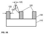
ここで図面を参照する。図中、同様の参照番号は同一又は対応する部材を表す。図1A〜図1A及び図2は、本発明の実施例による基板のパターニング方法を表している。当該方法は、フローチャート200で表され、かつ、基板110上に放射線感受性材料層120を形成する工程から始まる。放射線感受性材料層120はフォトレジストを含んで良い。たとえば放射線感受性材料層120は、248nmレジスト、193nmレジスト、157nmレジスト、EUV(極紫外)レジスト、又は電子ビーム感受性レジストを含んで良い。さらにたとえば放射線感受性材料層120は、熱硬化フォトレジスト、電磁(EM)放射線硬化フォトレジスト、又は化学硬化フォトレジストを含んで良い。 Reference is now made to the drawings. In the drawings, like reference numerals indicate identical or corresponding members. 1A to 1A and 2 illustrate a substrate patterning method according to an embodiment of the present invention. The method is represented by
放射線感受性材料層120は、基板110上に材料をスピンコーティングすることによって形成されて良い。放射線感受性材料の第1層120は、トラックシステムを用いて形成されて良い。たとえばトラックシステムは、東京エレクトロン株式会社から市販されているClean Track ACT8(登録商標)、Clean Track ACT12(登録商標)、LITHIUS(登録商標)、LITHIUS Pro(商標)、又はLITHIUS Pro V(商標)レジストコーティング及び現像システムを含んで良い。基板上にフォトレジスト膜を形成する他のシステム及び方法は当業者に周知である。コーティングプロセスに続いて、基板110を加熱する1つ以上の第1堆積後ベーキング(PAB)及び前記PAB後に基板110を冷却する1つ以上の冷却サイクルが行われて良い。 The radiation
220と図1Bに示されているように、パターン122が放射線感受性材料層120中に準備される。放射線感受性材料層120を有する基板110は、放射線露光システム内の位置合わせ位置にて位置合わせされ、かつ、画像パターンを有する放射線によって結像される。放射線露光システムは、乾式又は湿式フォトリソグラフィシステムを有して良い。画像パターンは、任意の適切なステッピングリソグラフィシステム又は走査リソグラフィシステムを用いて形成されて良い。たとえばフォトリソグラフィシステムは、ASML社又はキャノンUSAから市販されている。あるいはその代わりに画像パターンは、電子ビームリソグラフィシステムを用いて形成されて良い。 A
画像パターン領域を除去し、かつ、放射線感受性材料層120中にパターン122を形成するため、画像パターンに曝露された放射線感受性材料層120には現像プロセスが施される。パターン122は限界寸法(CD)124と粗さ125によって特徴付けられて良い。粗さ125は、ライン端粗さ(LER)及び/又はライン幅粗さ(LWR)を含んで良い。パターン122はラインパターンを含んで良い。現像プロセスは、現像システム−たとえばトラックシステム−中で基板を現像溶液に曝す工程を含んで良い。たとえばトラックシステムは、東京エレクトロン株式会社から市販されているClean Track ACT8(登録商標)、Clean Track ACT12(登録商標)、LITHIUS(登録商標)、LITHIUS Pro(商標)、又はLITHIUS Pro V(商標)レジストコーティング及び現像システムを含んで良い。現像プロセスに先立って、基板110を加熱する1つ以上の第1露光後ベーキング(PEB)及び該1つ以上の第1PEBに続いて基板110を冷却する冷却サイクルが行われて良い。 In order to remove the image pattern area and form the
230と図1Cに示されているように、放射線感受性材料層120中でのパターン122の準備に続いて、限界寸法(CD)スリム化プロセスが実行されることで、CD124は減少したCD134となる。図3はCDスリム化プロセスを表している。図9Aと図9Bは、CDスリム化プロセスの典型的データを表している。 230 and FIG. 1C, following the preparation of the
240と図1Cに示されているように、放射線感受性材料層120中でのパターン122の準備に続いて、平滑化プロセスが実行されることで、粗さ125は減少した粗さ135となる。図4A〜図4Eは平滑化プロセス−たとえば蒸気平滑化プロセス−を表している。図10Aと図10Bは、蒸気平滑化プロセスの典型的データを表している。 As shown in 240 and FIG. 1C, following the preparation of the
上述したように、平滑化プロセスは、蒸気(気相)平滑化プロセスを含んで良い。しかし平滑化プロセスは、液体(液相)平滑化プロセス又は蒸気平滑化プロセスと液体平滑化プロセスの組み合わせを含んでも良い。たとえば液体平滑化プロセスは、1つ以上の界面活性剤含有洗浄プロセスを含んで良い。界面活性剤含有洗浄プロセスのさらなる詳細については特許文献3を参照のこと。 As described above, the smoothing process may include a vapor (gas phase) smoothing process. However, the smoothing process may include a liquid (liquid phase) smoothing process or a combination of a vapor smoothing process and a liquid smoothing process. For example, the liquid smoothing process may include one or more surfactant-containing cleaning processes. See Patent Document 3 for further details of the surfactant-containing cleaning process.
平滑化プロセスはさらに、熱処理−たとえば基板温度の上昇−を含んで良い。平滑化プロセスはさらに、電磁(EM)放射線−たとえば紫外(UV)放射線、マイクロ波放射線、又は電子ビーム放射線−への曝露を含んで良い。 The smoothing process may further include a heat treatment, such as increasing the substrate temperature. The smoothing process may further include exposure to electromagnetic (EM) radiation, such as ultraviolet (UV) radiation, microwave radiation, or electron beam radiation.
図3で表されているように、CDスリム化プロセスは、基板310上に形成されて内部にはパターン321が準備される放射線感受性材料層320を有する基板310を受け取る工程から始まるプロセスシーケンス300を含む。上述したように、フォトリソグラフィシステム内で電磁(EM)放射線に放射線感受性材料層320を曝露した後、放射線感受性材料層320を第1現像溶液に曝すことで、CD325を有するパターン321が残されることによって、放射線感受性材料層320は現像される。放射線感受性材料層320をEM放射線に曝露する間、パターン321の(影付けされた)一部分は、中程度の強度のEM放射線に曝露されるが、第1現像溶液に曝された後でも残る。 As depicted in FIG. 3, the CD slimming process comprises a process sequence 300 that begins with receiving a
301では、さらに放射線感受性材料層320を昇温した状態で第2現像溶液に曝すことによって、放射線感受性材料層320は現像される。そのようにする際、昇温した状態の第2現像溶液は、中程度の強度のEM放射線に曝露されるパターン321の(影付けされた)一部分を除去する。その結果、中程度に減少したCD326を有する中間パターン322が残る。例として、第2現像溶液は、約23℃以上の熱現像温度に昇温されたTMAH含有溶液を含んで良い。あるいはその代わりに例として、第2現像溶液は、約25℃以上の熱現像温度に昇温されたTMAH含有溶液を含んで良い。第2現像溶液は、約30℃以上の熱現像温度に昇温されたTMAH含有溶液を含んで良い。第2現像溶液は、約23℃以上で約50℃以下の熱現像温度に昇温されたTMAH含有溶液を含んで良い。あるいはその代わりに、第2現像溶液は、約30℃以上で約50℃以下の熱現像温度に昇温されたTMAH含有溶液を含んで良い。このプロセス工程では、現像溶液の濃度、温度、曝した時間が、パターンCD制御を実現するために調節されるプロセスパラメータである。 In 301, the radiation
302では、中程度に減少したCD326を有する中間パターン322が、酸性(”+”の符号及び/又はH+によって表される)溶液によって処理される。例として、酸含有溶液は、上述したように、スピンコーティングによって中程度に減少したCD326を有する放射線感受性材料層320に塗布されて良い。このプロセス工程では、酸含有溶液の濃度、温度、曝した時間が、パターンCD制御を実現するために調節されるプロセスパラメータである。At 302, an
303では、放射線感受性材料層320は、酸が放射線感受性材料層320中に入り込むように拡散する温度にまで昇温される。例として、放射線感受性材料層320は、約50℃以上のベーキング温度にまで昇温される。あるいはその代わりに、例として、放射線感受性材料層320は、約50℃〜約180℃の範囲のベーキング温度にまで昇温される。このプロセス工程では、温度と曝した時間が、パターンCD制御を実現するために調節されるプロセスパラメータである。 At 303, the radiation
304では、放射線感受性材料層320は、放射線感受性材料層320を第3現像溶液に曝すことによってさらに現像される。そのようにする際、第3現像溶液は、放射線感受性材料層320中に減少したCD335を有する最終パターン323を生成する。例として、第3現像溶液は、室温のTMAH含有溶液を含んで良い。このプロセス工程では、温度と曝した時間が、パターンCD制御を実現するために調節されるプロセスパラメータである。 At 304, the radiation
CDスリム化プロセスについてのさらなる詳細については特許文献4を参照のこと。CDスリム化プロセスについての他の詳細については特許文献5〜8を参照のこと。 See
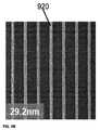
図9Aと図9Bに示されているように、CDスリム化プロセスが実行されることで、約50nmの第1ラインCD910は約29.2nmの第2ラインCD920となる。 As shown in FIGS. 9A and 9B, when the CD slimming process is performed, the first line CD910 of about 50 nm becomes the second line CD920 of about 29.2 nm.
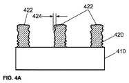
図4A〜図4Eで図示されているように、平滑化プロセスは、基板410上に形成されて内部にはパターン422が準備される放射線感受性材料層420を有する基板410を受け取る工程から始まるプロセスシーケンス300を含む。上述したように、フォトリソグラフィシステム内で電磁(EM)放射線に放射線感受性材料層420を曝露した後、放射線感受性材料層420を現像溶液に曝すことで、放射線感受性材料層420は現像される。その結果、粗さ424を有するパターン422が残される。 As illustrated in FIGS. 4A-4E, the smoothing process begins with receiving a
上述したように、平滑化プロセスは気相平滑化プロセスを含んで良い。そこでは図4Bに示されているように、放射線感受性材料層420中のパターン422が気相環境430に曝される。一の実施例では、気相環境430は、N-メチルピロリダン又はN-メチル-2-ピロリダンを含む処理蒸気を含んで良い。たとえばたとえば基板410は、噴霧状処理溶液に曝されて良い。それに加えて、基板410上のパターン422を処理蒸気に曝している間、基板温度が昇温するように基板は加熱されて良い。基板温度は、約20℃〜約100℃の範囲であって良く、好適には約30℃〜約50℃の範囲であって良い。さらに基板410上のパターン422を処理蒸気に曝露している間、基板には電磁(EM)放射線が照射されて良い。このプロセス工程では、気相環境の圧力と曝した時間が、粗さの減少すなわち制御を実現するために調節されるプロセスパラメータである。 As described above, the smoothing process may include a gas phase smoothing process. There, the
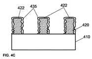
図4Cに図示されているように、内部にパターン422が準備された放射線感受性材料層420を気相環境430に曝した結果として、化学処理された表面層435が生成される。気相環境430は、放射線感受性材料層420の曝された部分と反応する。その結果、化学処理された表面層435内の放射線感受性材料の「融解」すなわちリフローが起こることで、放射線感受性材料層420の曝された表面は平滑化する(図4D参照)。 As illustrated in FIG. 4C, as a result of exposing the radiation
その後図4Eに図示されているように、パターン422には乾燥処理が施されることで、気相環境430への曝露からの残留物が除去される。乾燥プロセスは、大気圧又は真空圧でのスピン乾燥プロセスを含んで良い。乾燥プロセスはさらに、パターン422上に乾燥流体を供給する工程を含んで良い。乾燥流体は気相又は液相であって良い。たとえば乾燥流体はイソプロピルアルコール(IPA)を含んで良い。 Thereafter, as illustrated in FIG. 4E, the
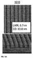
図10Aと図10Bに図示されているように、蒸気平滑化プロセスが実行されることで、63.8nmのラインCDを有する約5.7mmの第1ライン幅粗さ(LWR)1010は、64.7nmのラインCDを有する約3.8mmの第2LWR1020となる。 As illustrated in FIGS.10A and 10B, the vapor smoothing process is performed so that a first line width roughness (LWR) 1010 of about 5.7 mm with a line CD of 63.8 nm is 64.7 nm. The second LWR1020 is about 3.8mm with line CD.
平滑化プロセスは、CDスリム化プロセスに先んじて(図3のシーケンスの位置401を参照のこと)、CDスリム化プロセスの後(図3のシーケンスの位置404を参照のこと)、又はCDスリム化プロセスの間(図3のシーケンスの位置402,403を参照のこと)に実行されて良い。CDスリム化プロセスの間、平滑化プロセスは、熱源像温度に昇温された第2現像溶液の供給後であって酸を含む処理化合物による基板の処理に先んじて(図3のシーケンスの位置402を参照のこと)実行されて良い。あるいはその代わりに、CDスリム化プロセスの間、平滑化プロセスは、酸を拡散させるように基板をベーキングする後であって第3現像溶液の供給後に(図3のシーケンスの位置403を参照のこと)実行されて良い。あるいはその代わりに、減少した粗さをさらに減少した粗さにするように、1つ以上のさらなる平滑化プロセスが実行されても良い。 The smoothing process precedes the CD slimming process (see
基板をパターニングする方法はさらに、平滑化プロセス直前に評価された平滑化前の粗さ(つまり図1Aの粗さ125)を決定し、かつ、平滑化プロセス直後に評価された平滑化後の粗さ(つまり図1Cの粗さ135)を決定することによって粗さを評価する工程、及び、10%を超える粗さの減少を実現する工程をさらに含んで良い。ここで粗さの減少は、平滑化前の処理粗さに対する平滑化処理前の粗さと平滑化後の粗さとの差のパーセント表示の比として測定される。さらに平滑化プロセスは30%を超える粗さの減少を実現しうる。またさらに平滑化プロセスは50%を超える粗さの減少を実現しうる。 The method for patterning the substrate further determines the pre-smoothness roughness evaluated immediately before the smoothing process (ie, the
ここで図5A〜図5Gと図6を参照すると、本発明の他の実施例による基板のダブルパターニング方法が表されている。ダブルパターニング方法は、リソ-エッチング-リソ-エッチング(LELE)法、リソ-リソ-エッチング(LLE)法、又はリソ-硬化-リソ-エッチング(LFLE)法を含んで良い。 Referring now to FIGS. 5A-5G and FIG. 6, a double patterning method for a substrate according to another embodiment of the present invention is illustrated. Double patterning methods may include a litho-etch-litho-etch (LELE) method, a litho-litho-etch (LLE) method, or a litho-curing-litho-etch (LFLE) method.
LELEダブルパターニングでは、基板が第1パターンに曝露され、第1パターンは放射線感受性材料内で現像され、放射線感受性材料内に形成された第1パターンは、エッチングプロセスを用いることによって下地層へ転写され、その後この一連の工程が第2パターンについて繰り返される。上述したように、CDスリム化プロセスは、第1パターンのCDの減少、第2パターンのCDの減少、又は、第1パターンと第2パターン両方のCDの減少に利用されて良い。さらに上述したように、平滑化プロセスは、第1パターンの粗さの減少、第2パターンの粗さの減少、又は、第1パターンと第2パターン両方の粗さの減少に利用されて良い。 In LELE double patterning, the substrate is exposed to a first pattern, the first pattern is developed in a radiation sensitive material, and the first pattern formed in the radiation sensitive material is transferred to the underlying layer by using an etching process. Thereafter, this series of steps is repeated for the second pattern. As described above, the CD slimming process may be used to reduce the CD of the first pattern, the CD of the second pattern, or the CD of both the first pattern and the second pattern. Further, as described above, the smoothing process may be used to reduce the roughness of the first pattern, the roughness of the second pattern, or the roughness of both the first pattern and the second pattern.
LLEダブルパターニングでは、基板が第1パターンに曝露され、基板が第2パターンに曝露され、第1パターンと第2パターンは放射線感受性材料内で現像され、かつ、放射線感受性材料内に形成された第1パターンと第2パターンは、エッチングプロセスを用いることによって下地層へ転写される。上述したように、CDスリム化プロセスは、第1パターンのCDの減少、第2パターンのCDの減少、又は、第1パターンと第2パターン両方のCDの減少に利用されて良い。さらに上述したように、平滑化プロセスは、第1パターンの粗さの減少、第2パターンの粗さの減少、又は、第1パターンと第2パターン両方の粗さの減少に利用されて良い。 In LLE double patterning, the substrate is exposed to the first pattern, the substrate is exposed to the second pattern, the first pattern and the second pattern are developed in the radiation sensitive material, and the first pattern formed in the radiation sensitive material. The first pattern and the second pattern are transferred to the underlayer by using an etching process. As described above, the CD slimming process may be used to reduce the CD of the first pattern, the CD of the second pattern, or the CD of both the first pattern and the second pattern. Further, as described above, the smoothing process may be used to reduce the roughness of the first pattern, the roughness of the second pattern, or the roughness of both the first pattern and the second pattern.
LLEダブルパターニングへの一の方法はリソ-硬化-リソ-エッチング(LFLE)法を含む。LFLE法は、第1パターニング層中の第1パターン上への硬化材料の堆積を利用する。第1パターニング層中の第1パターン上へ硬化材料が堆積されることで、「硬化」すなわち架橋が内部で起こり、第1パターニング層は、第2パターンを有する第2パターニング層の後続の処理に耐えることが可能となる。ここでLFLEダブルパターニング法についてより詳細に説明する。 One method for LLE double patterning includes litho-curing-litho-etching (LFLE). The LFLE method utilizes the deposition of a curable material on the first pattern in the first patterning layer. By depositing a curable material onto the first pattern in the first patterning layer, "curing" or cross-linking occurs internally, and the first patterning layer is subject to subsequent processing of the second patterning layer having the second pattern. It becomes possible to endure. Here, the LFLE double patterning method will be described in more detail.
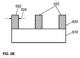
当該方法が、フローチャート600で表され、かつ、基板510上に放射線感受性材料層520を形成する工程から始まる。放射線感受性材料層520はフォトレジストを含んで良い。たとえば放射線感受性材料層520は、248nmレジスト、193nmレジスト、157nmレジスト、EUV(極紫外)レジスト、又は電子ビーム感受性レジストを含んで良い。さらにたとえば放射線感受性材料層120は、熱硬化フォトレジスト、電磁(EM)放射線硬化フォトレジスト、又は化学硬化フォトレジストを含んで良い。 The method is represented by
放射線感受性材料層520は、基板510上に材料をスピンコーティングすることによって形成されて良い。放射線感受性材料の第1層520は、トラックシステムを用いて形成されて良い。たとえばトラックシステムは、東京エレクトロン株式会社から市販されているClean Track ACT8(登録商標)、Clean Track ACT12(登録商標)、LITHIUS(登録商標)、LITHIUS Pro(商標)、又はLITHIUS Pro V(商標)レジストコーティング及び現像システムを含んで良い。基板上にフォトレジスト膜を形成する他のシステム及び方法は当業者に周知である。コーティングプロセスに続いて、基板510を加熱する1つ以上の第1堆積後ベーキング(PAB)及び前記PAB後に基板510を冷却する1つ以上の冷却サイクルが行われて良い。 The radiation
620と図5Bに示されているように、放射線感受性材料層520を有する基板510は、放射線露光システム内の第1位置合わせ位置にて位置合わせされ、かつ、第1画像パターンを有する第1放射線によって結像される。放射線露光システムは、乾式又は湿式フォトリソグラフィシステムを有して良い。第1画像パターンは、任意の適切なステッピングリソグラフィシステム又は走査リソグラフィシステムを用いて形成されて良い。たとえばフォトリソグラフィシステムは、ASML社又はキャノンUSAから市販されている。あるいはその代わりに画像パターンは、電子ビームリソグラフィシステムを用いて形成されて良い。 As shown in 620 and FIG. 5B, a
第1画像パターン領域を除去し、かつ、放射線感受性材料の第1層520中に第1パターン522を形成するため、第1画像パターンに曝露された放射線感受性材料の第1層520には現像プロセスが施される。第1パターン522は第1限界寸法(CD)524と第1粗さによって特徴付けられて良い。第1パターン522は第1ラインパターンを含んで良い。現像プロセスは、現像システム−たとえばトラックシステム−中で基板を現像溶液に曝す工程を含んで良い。たとえばトラックシステムは、東京エレクトロン株式会社から市販されているClean Track ACT8(登録商標)、Clean Track ACT12(登録商標)、LITHIUS(登録商標)、LITHIUS Pro(商標)、又はLITHIUS Pro V(商標)レジストコーティング及び現像システムを含んで良い。現像プロセスに先立って、基板510を加熱する1つ以上の第1露光後ベーキング(PEB)及び該1つ以上の第1PEBに続いて基板510を冷却する冷却サイクルが行われて良い。 The
630と図5Cに示されているように、第1限界寸法(CD)スリム化プロセスが実行されることで、第1CD524は第1の減少したCD526となる。図3はCDスリム化プロセスを表している。図9Aと図9Bは、CDスリム化プロセスの典型的なデータを表している。 As shown in 630 and FIG. 5C, the first critical dimension (CD) slimming process is performed so that the first CD524 becomes the first reduced CD526. Fig. 3 shows the CD slimming process. 9A and 9B represent typical data for the CD slimming process.
635では、第1平滑化プロセスが実行されることで、第1粗さは第1の減少した粗さとなる。図4A〜図4Eは、蒸気平滑化プロセスを表している。図10Aと図10Bは、蒸気平滑化プロセスの典型的なデータを表している。第1平滑化プロセスは、第1CDスリム化プロセスの前、第1CDスリム化プロセスの間、又は第1CDスリム化プロセスの後に行われて良い。 In 635, the first smoothing process is performed so that the first roughness becomes the first reduced roughness. 4A-4E represent the steam smoothing process. 10A and 10B represent typical data for the steam smoothing process. The first smoothing process may be performed before the first CD slimming process, during the first CD slimming process, or after the first CD slimming process.
640と図5Dに示されているように、前記放射線感受性材料の第1層520中の第1の減少したCD526と第1粗さを有する第1パターン522が、硬化プロセスを用いることによって硬化されることで、放射線感受性材料の硬化した第1層520’が形成される。一の実施例では、前記放射線感受性材料の第1層520は、熱的に硬化可能な硬化レジストを含んで良い。硬化プロセスを用いることによって放射線感受性材料の第1層520中で第1パターン522を硬化する工程は、放射線感受性材料の第1層520をベーキング(加熱)することで、第1の減少したCD526を有する第1パターンを熱的に硬化して保持する工程を含む。硬化プロセス中、温度とベーキング時間が、パターンCD制御を実現するために調節されうるプロセスパラメータである。 640 and the
限定ではなく以降で説明するが、本願明細書で用いられている「硬化(freeze)」という語句は、放射線感受性材料層が、その放射線感受性材料層が、後続のリソグラフィ処理に耐えられるように放射線感受性材料層の条件を変更するように準備及び/又は処理されるプロセス(の結果)を表す。たとえば一旦パターンが放射線感受性材料層中で硬化されると、さらなるリソグラフィプロセスに続くパターンCDの多少の変化の有無にかかわらず、そのパターンは実質的に残る。 Although described below and not limitation, the phrase “freeze” as used herein refers to a radiation-sensitive material layer so that the radiation-sensitive material layer can withstand subsequent lithographic processing. Represents a (result) of a process that is prepared and / or processed to change the conditions of the sensitive material layer. For example, once the pattern is cured in the radiation sensitive material layer, the pattern remains substantially with or without some change in the pattern CD following the further lithographic process.
他の実施例では、放射線感受性材料の第1層520は、電磁(EM)放射線により硬化可能な硬化レジストを含んで良い。ここで硬化プロセスを用いることによって放射線感受性材料の第1層520中の第1パターン522を硬化する工程は、放射線感受性材料の第1層520をEM放射線に曝露することで、第1の減少したCD526を有する第1パターン522を放射線によって硬化して保持する工程を含む。硬化プロセス中、曝露のEM強度と時間が、パターンCD制御のために調節されうるプロセスパラメータである。 In other embodiments, the
さらに他の実施例では、放射線感受性材料の第1層520は化学的に硬化可能な硬化レジストを含んで良い。ここで硬化プロセスを用いることによって放射線感受性材料の第1層520中の第1パターンを硬化する工程は、化学硬化材料を放射線感受性材料の第1層520に塗布して、その化学硬化材料と放射線感受性材料の第1層520とを反応させることで、第1の減少したCD526を有する第1パターン522を化学的に硬化して保持する工程を含む。硬化プロセス中、化学硬化材料の濃度と種類及び曝す時間が、パターンCD制御を実現するように調節されうるプロセスパラメータである。 In yet another embodiment, the first layer of radiation
ここで化学硬化材料は、放射線感受性材料の第1層520と化学的に相互作用するように、放射線感受性材料の第1層520全体にわたって塗布されて良い。化学硬化材料は、基板510上に材料をスピンコーティングすることによって形成されて良い。化学硬化材料はトラックシステムを用いて生成されて良い。たとえばトラックシステムは、東京エレクトロン株式会社から市販されているClean Track ACT8(登録商標)、Clean Track ACT12(登録商標)、LITHIUS(登録商標)、LITHIUS Pro(商標)、又はLITHIUS Pro V(商標)レジストコーティング及び現像システムを含んで良い。基板上にフォトレジスト膜を形成する他のシステム及び方法は当業者に周知である。コーティングプロセスに続いて、基板510を加熱して化学硬化材料の少なくとも一部を硬化させる1つ以上のベーキングプロセスが行われて良い。 Here, the chemically curable material may be applied throughout the
化学硬化材料を基板510へ塗布して、基板510を加熱する結果として、化学硬化材料の一部が放射線感受性材料の第1層520の曝露した表面と反応することで、放射線感受性材料の硬化した第1層520’が形成される。その後化学硬化材料は、剥離溶液を用いることによって基板510から剥離される。それによって放射線感受性材料の硬化した第1層520’中の第1パターン522は保持される。剥離溶液は従来の剥離溶液又は高規定度の剥離溶液を含んで良い。たとえば剥離溶液は、0.26よりも大きな規定度(N)を有する活性溶液を含む。あるいはその代わりに剥離溶液は、0.3よりも大きな規定度(N)を有する活性溶液を含む。あるいはその代わりに剥離溶液は、0.4よりも大きな規定度(N)を有する活性溶液を含む。あるいはその代わりに剥離溶液は、0.5よりも大きな規定度(N)を有する活性溶液を含む。 As a result of applying the chemically curable material to the
剥離溶液は水性アルカリ溶液を含んで良い。それに加えて剥離溶液は水酸化物を含んで良い。それに加えて剥離溶液は第4級水酸化アンモニウムを含んで良い。さらに剥離溶液は、水酸化テトラメチルアンモニウム(TMAH)を含んで良い。剥離溶液中でのTMAHの規定度(N)は0.26以上であって良い。あるいはその代わりに剥離溶液中でのTMAHの規定度(N)は0.3以上であって良い。あるいはその代わりに剥離溶液中でのTMAHの規定度(N)は0.4以上であって良い。あるいはその代わりに剥離溶液中でのTMAHの規定度(N)は0.5以上であって良い。あるいはその代わりに剥離溶液中でのTMAHの規定度(N)は約0.32であって良い。剥離溶液中でのTMAHの濃度は2.36%w/v(すなわち100mlの溶液あたり2.36gの溶質)以上であって良い。あるいはその代わりに剥離溶液中でのTMAHの濃度は2.72%w/v(すなわち100mlの溶液あたり2.72gの溶質)以上であって良い。従来の剥離溶液は0.26以下の規定度(N)を有する。たとえばTMAH系剥離溶液は、規定度0.26であれば市販されている。規定度(N)が0.26よりも大きくなることで、ダブルパターニングの基板スループットが増大し、かつ、デバイスの歩留まりに影響する基板の欠陥が減少する。 The stripping solution may include an aqueous alkaline solution. In addition, the stripping solution may contain hydroxide. In addition, the stripping solution may contain quaternary ammonium hydroxide. Further, the stripping solution may contain tetramethylammonium hydroxide (TMAH). The normality (N) of TMAH in the stripping solution may be 0.26 or more. Alternatively, the normality (N) of TMAH in the stripping solution may be 0.3 or more. Alternatively, the normality (N) of TMAH in the stripping solution may be 0.4 or more. Alternatively, the normality (N) of TMAH in the stripping solution may be 0.5 or more. Alternatively, the normality (N) of TMAH in the stripping solution may be about 0.32. The concentration of TMAH in the stripping solution may be greater than 2.36% w / v (ie 2.36 g solute per 100 ml solution). Alternatively, the concentration of TMAH in the stripping solution may be 2.72% w / v (ie, 2.72 g solute per 100 ml solution) or higher. Conventional stripping solutions have a normality (N) of 0.26 or less. For example, a TMAH stripping solution is commercially available with a normality of 0.26. When the normality (N) is greater than 0.26, the double patterning substrate throughput is increased and the substrate defects that affect device yield are reduced.
各実施例では、硬化プロセスは、第1パターン522の一部又は全体にわたって広がる保護層を生成する。前記保護層は、後続のリソグラフィプロセス−たとえばコーティング、露光、現像、及びスリム化プロセス−から放射線感受性材料の第1層中の第1パターンを保護する。その結果、放射線感受性材料の第1層が「硬化」されることで、第1の減少したCDによって特徴付けられる放射線感受性材料の硬化した第1層520’が形成される。 In each embodiment, the curing process produces a protective layer that extends over part or all of the
放射線感受性材料の第1層−熱的に硬化可能なレジスト、EMにより硬化可能なレジスト、又は化学的に硬化可能なレジストのいずれか−は、熱的に処理され、放射線により処理され、又は化学的に処理されるときに架橋を示す材料を含んで良い。それに加えて化学硬化材料は、放射線感受性材料層内で架橋を引き起こしうる任意の除去可能な材料を含んで良い。化学硬化材料は高分子材料を含んで良い。たとえばこれらの材料は、JSRマイクロから市販されている材料−たとえばFZX F112硬化材料を含む−を含んで良い。あるいはその代わりに、たとえばこれらの材料は、ダウ・ケミストリーの100%子会社であるローム・アンド・ハースから市販されている材料−たとえばSC1000Surface
Curing Agents(SCA)(商標)−を含んで良い。The first layer of radiation sensitive material—either a thermally curable resist, an EM curable resist, or a chemically curable resist—is thermally processed, treated with radiation, or chemically. May include materials that exhibit cross-linking when processed mechanically. In addition, the chemically curable material may include any removable material that can cause crosslinking within the radiation sensitive material layer. The chemical curable material may include a polymeric material. For example, these materials may include materials commercially available from JSR Micro, including, for example, FZX F112 curable materials. Alternatively, for example, these materials are commercially available from Rohm & Haas, a wholly owned subsidiary of Dow Chemistry—for example, SC1000 Surface
Curing Agents (SCA) ™.
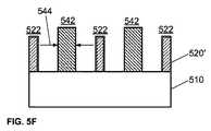
650と図5Eに示されているように、放射線感受性材料の第2層540が基板510上に形成される。放射線感受性材料の第2層540はフォトレジストを含んで良い。たとえば放射線感受性材料の第2層540は、248nmレジスト、193nmレジスト、157nmレジスト、EUV(極紫外)レジスト、又は電子ビーム感受性レジストを含んで良い。放射線感受性材料の第2層540は、基板510上に材料をスピンコーティングすることによって形成されて良い。放射線感受性材料の第2層540は、トラックシステムを用いて形成されて良い。たとえばトラックシステムは、東京エレクトロン株式会社から市販されているClean Track ACT8(登録商標)、Clean Track ACT12(登録商標)、LITHIUS(登録商標)、LITHIUS Pro(商標)、又はLITHIUS Pro V(商標)レジストコーティング及び現像システムを含んで良い。基板上にフォトレジスト膜を形成する他のシステム及び方法は当業者に周知である。コーティングプロセスに続いて、基板510を加熱する1つ以上の第2PAB及び前記1つ以上の第2PAB後に基板510を冷却する1つ以上の冷却サイクルが行われて良い。 As shown in 650 and FIG. 5E, a
660と図5Fに示されているように、放射線感受性材料の第2層540を有する基板510は、放射線露光システム内の第2位置合わせ位置にて位置合わせされ、かつ、第2画像パターンを有する第2放射線によって結像される。第2放射線は第1放射線と同一であっても良いし、異なっていても良い。放射線露光システムは、乾式又は湿式フォトリソグラフィシステムを有して良い。第2画像パターンは、任意の適切なステッピングリソグラフィシステム又は走査リソグラフィシステムを用いて形成されて良い。たとえばフォトリソグラフィシステムは、ASML社又はキャノンUSAから市販されている。あるいはその代わりに第2画像パターンは、電子ビームリソグラフィシステムを用いて形成されて良い。 As shown in 660 and FIG. 5F, a
第2画像パターン領域を除去し、かつ、放射線感受性材料の第2層540中に第2パターン542を形成するため、第2画像パターンに曝露された放射線感受性材料の第2層540には現像プロセスが施される。第2パターン542は第2限界寸法(CD)544と第2粗さによって特徴付けられて良い。第2パターン542は第2ラインパターンを含んで良い。現像プロセスは、現像システム−たとえばトラックシステム−中で基板を現像溶液に曝す工程を含んで良い。たとえばトラックシステムは、東京エレクトロン株式会社から市販されているClean Track ACT8(登録商標)、Clean Track ACT12(登録商標)、LITHIUS(登録商標)、LITHIUS Pro(商標)、又はLITHIUS Pro V(商標)レジストコーティング及び現像システムを含んで良い。現像プロセスに先立って、基板510を加熱する1つ以上の第2PEB及び該1つ以上の第2PEBに続いて基板510を冷却する冷却サイクルが行われて良い。 A development process is applied to the
670と図5Gに示されているように、第2限界寸法(CD)スリム化プロセスが実行されることで、第2CD544は第2の減少したCD546となる。図3はCDスリム化プロセスを表している。図9Aと図9Bは、CDスリム化プロセスの典型的なデータを表している。 As shown in 670 and FIG. 5G, the second critical dimension (CD) slimming process is performed, so that the
675では、第2平滑化プロセスが実行されることで、第2粗さは第2の減少した粗さとなる。図4A〜図4Eは、蒸気平滑化プロセスを表している。図10Aと図10Bは、蒸気平滑化プロセスの典型的なデータを表している。第2平滑化プロセスは、第2CDスリム化プロセスの前、第2CDスリム化プロセスの間、又は第2CDスリム化プロセスの後に行われて良い。 At 675, the second smoothing process is performed so that the second roughness becomes the second reduced roughness. 4A-4E represent the steam smoothing process. 10A and 10B represent typical data for the steam smoothing process. The second smoothing process may be performed before the second CD slimming process, during the second CD slimming process, or after the second CD slimming process.
680では、ダブルパターン550−第1の減少したCD526と第1の減少した粗さを有する第1パターン522及び第2の減少したCD546と第2の減少した粗さを有する第2パターン542を含む−が、1つ以上のエッチングプロセスを用いることによって基板510の下地の層へ転写される。1つ以上のエッチングプロセスは湿式又は乾式エッチングプロセスの任意の組み合わせを含んで良い。乾式エッチングプロセスは乾式プラズマエッチングプロセス又は乾式非プラズマエッチングプロセスを含んで良い。 680 includes a double pattern 550-a
第1CDスリム化プロセス、第1平滑化プロセス、第2CDスリム化プロセス、第2平滑化プロセス、硬化プロセス、第1リソグラフィプロセス、若しくは第2リソグラフィプロセス、又はこれら2つ以上の組み合わせについての少なくとも1つのプロセスパラメータは、第1パターンと第2パターンの破損を防止するように最適化されて良い。さらに第1CDスリム化プロセス、第1平滑化プロセス、第2CDスリム化プロセス、第2平滑化プロセス、硬化プロセス、第1リソグラフィプロセス、若しくは第2リソグラフィプロセス、又はこれら2つ以上の組み合わせについての少なくとも1つのプロセスパラメータは、硬化プロセスが施された第1パターン中の第1の減少したCDへの影響を最小限にしながら第2パターン中に第2の減少したCDを生成するように最適化されて良い。 At least one of the first CD slimming process, the first smoothing process, the second CD slimming process, the second smoothing process, the curing process, the first lithography process, the second lithography process, or a combination of two or more thereof The process parameters may be optimized to prevent damage to the first pattern and the second pattern. Further, at least one of the first CD slimming process, the first smoothing process, the second CD slimming process, the second smoothing process, the curing process, the first lithography process, the second lithography process, or a combination of two or more thereof Two process parameters are optimized to produce a second reduced CD in the second pattern while minimizing the impact on the first reduced CD in the first pattern subjected to the curing process good.
例として、第1パターンの第1CD及び/又は第2パターンの第2CDは、減少したCDと減少した粗さを有する第1パターンと第2パターンの最適印刷を実現するように調節されて良い。あるいはその代わりに例として、第1CDと第1の減少したCDとの間での減少量、第1粗さと第1の減少した粗さとの間での減少量、第2CDと第2の減少したCDとの間での減少量、及び/又は第2粗さと第2の減少した粗さとの間での減少量は、減少したCDと減少した粗さを有する第1パターンと第2パターンの最適印刷を実現するように調節されて良い。 As an example, the first CD of the first pattern and / or the second CD of the second pattern may be adjusted to achieve optimal printing of the first pattern and the second pattern with reduced CD and reduced roughness. Or alternatively, as an example, the amount of reduction between the first CD and the first reduced CD, the amount of reduction between the first roughness and the first reduced roughness, the second CD and the second reduction The amount of reduction between the CD and / or the amount of reduction between the second roughness and the second reduced roughness is the optimum of the first and second patterns with reduced CD and reduced roughness. It can be adjusted to achieve printing.
一の実施例では、第2CDスリム化プロセスは、第1パターン中の第1の減少したCDへの影響を最小限に抑制しながら、第2パターン中の第2の減少したCDを実現するように設計されて良い。たとえば第1リソグラフィプロセスと第2リソグラフィプロセスが実行されることで、実質的すなわち近似的に等しい第1CDと第2CDが印刷されて良い。その後、第1CDスリム化プロセスは第1CDを第1の減少したCDへ減少させ、第2CDスリム化プロセスは、第1の減少したCDへ影響しないように第2CDを第2の減少したCDへ減少させる。その結果第1の減少したCDと第2の減少したCDは実質的すなわち近似的に等しくなる。 In one embodiment, the second CD slimming process is adapted to achieve the second reduced CD in the second pattern while minimizing the impact on the first reduced CD in the first pattern. Can be designed to For example, a first lithographic process and a second lithographic process may be performed to print a first CD and a second CD that are substantially or approximately equal. The first CD slimming process then reduces the first CD to the first reduced CD, and the second CD slimming process reduces the second CD to the second reduced CD so as not to affect the first reduced CD. Let As a result, the first reduced CD and the second reduced CD are substantially or approximately equal.
他の実施例では、第2CDスリム化プロセスは、第1の減少したCDと第2の減少したCDの両方の減少を実現するように設計されて良い。たとえば第1リソグラフィプロセスと第2リソグラフィプロセスが実行されることで、第1CDと第2CDが実現されて良い。前記第1CDは、前記第2CDよりも大きく印刷される。それに加えてたとえば第1CDは、前記第2CDよりも最大で約5%大きく印刷される。それに加えてたとえば第1CDは、前記第2CDよりも最大で約10%大きく印刷される。それに加えてたとえば第1CDは、前記第2CDよりも最大で約15%大きく印刷される。それに加えてたとえば第1CDは、前記第2CDよりも最大で約25%大きく印刷される。それに加えてたとえば第1CDは、前記第2CDよりも約25%〜約50%大きく印刷される。それに加えてたとえば第1CDは、前記第2CDよりも約50%〜約75%大きく印刷される。その後、第1CDスリム化プロセスは第1CDを第1の減少したCDへ減少させ、第2CDスリム化プロセスは、第1の減少したCDを第3の減少したCDへさらに減少させながら、第2CDを第2の減少したCDへ減少させる。その結果第3の減少したCDと第2の減少したCDは実質的すなわち近似的に等しくなる。 In other embodiments, the second CD slimming process may be designed to achieve a reduction of both the first reduced CD and the second reduced CD. For example, the first CD and the second CD may be realized by executing the first lithography process and the second lithography process. The first CD is printed larger than the second CD. In addition, for example, the first CD is printed up to about 5% larger than the second CD. In addition, for example, the first CD is printed at a maximum of about 10% larger than the second CD. In addition, for example, the first CD is printed by about 15% larger than the second CD. In addition, for example, the first CD is printed up to about 25% larger than the second CD. In addition, for example, the first CD is printed about 25% to about 50% larger than the second CD. In addition, for example, the first CD is printed about 50% to about 75% larger than the second CD. The first CD slimming process then reduces the first CD to the first reduced CD, and the second CD slimming process further reduces the first CD to the third reduced CD, while reducing the second CD. Reduce to the second reduced CD. As a result, the third reduced CD and the second reduced CD are substantially or approximately equal.
ここで図7A〜図7J及び図8を参照すると、他の実施例による基板を多重パターニングする方法が記載されている。多重パターニング方法は、側壁画像転写(SIT)法を含んで良い。SIT法は、ダブルパターンを生成するように単一パターニング法(図1A〜図1C参照)と組み合わせられて良い。あるいはSIT法は、四重パターンを生成するようにダブルパターニング法(図7A〜図7G参照)と組み合わせられて良い。SIT法とLFLEダブルパターニング法との組み合わせについてここで詳細に説明する。 Referring now to FIGS. 7A-7J and 8, a method for multiple patterning a substrate according to another embodiment is described. Multiple patterning methods may include sidewall image transfer (SIT) methods. The SIT method may be combined with a single patterning method (see FIGS. 1A-1C) to generate a double pattern. Alternatively, the SIT method may be combined with the double patterning method (see FIGS. 7A-7G) to generate a quadruple pattern. The combination of the SIT method and the LFLE double patterning method will now be described in detail.
当該方法が、フローチャート800で示され、リソグラフィプロセスを用いることによって、限界寸法(CD)によって特徴付けられるパターンを放射線感受性材料層中に準備する工程で始まる。 The method begins at the step shown in
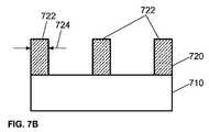
図7Aに図示されているように、パターンを準備する工程は、基板710上に放射線感受性材料の第1層720を形成する工程を含んで良い。放射線感受性材料層の第1層720はフォトレジストを含んで良い。たとえば放射線感受性材料の第1層720は、248nmレジスト、193nmレジスト、157nmレジスト、EUV(極紫外)レジスト、又は電子ビーム感受性レジストを含んで良い。さらにたとえば放射線感受性材料の第1層720は、熱硬化フォトレジスト、電磁(EM)放射線硬化フォトレジスト、又は化学硬化フォトレジストを含んで良い。 As shown in FIG. 7A, preparing the pattern may include forming a
放射線感受性材料の第1層720は、基板710上に材料をスピンコーティングすることによって形成されて良い。放射線感受性材料の第1層720は、トラックシステムを用いて形成されて良い。たとえばトラックシステムは、東京エレクトロン株式会社から市販されているClean Track ACT8(登録商標)、Clean Track ACT12(登録商標)、LITHIUS(登録商標)、LITHIUS Pro(商標)、又はLITHIUS Pro V(商標)レジストコーティング及び現像システムを含んで良い。基板上にフォトレジスト膜を形成する他のシステム及び方法は当業者に周知である。コーティングプロセスに続いて、基板710を加熱する1つ以上の第1堆積後ベーキング(PAB)及び前記1つ以上のPAB後に基板710を冷却する1つ以上の冷却サイクルが行われて良い。 A
図7Bに示されているように、パターンを準備する工程は、第1リソグラフィプロセスを用いることによって放射線感受性材料の第1層720中に第1パターン722を準備する工程をさらに含んで良い。ここで第1パターン722は第1限界寸法(CD)と第1粗さによって特徴付けられる。放射線感受性材料の第1層720を有する基板710は、放射線露光システム内の第1位置合わせ位置にて位置合わせされ、かつ、第1画像パターンを有する第1放射線によって結像される。放射線露光システムは、乾式又は湿式フォトリソグラフィシステムを有して良い。第1画像パターンは、任意の適切なステッピングリソグラフィシステム又は走査リソグラフィシステムを用いて形成されて良い。たとえばフォトリソグラフィシステムは、ASML社又はキャノンUSAから市販されている。あるいはその代わりに画像パターンは、電子ビームリソグラフィシステムを用いて形成されて良い。 As shown in FIG. 7B, the step of preparing the pattern may further include the step of preparing a
第1画像パターン領域を除去し、かつ、放射線感受性材料の第1層720中に第1パターン722を形成するため、第1画像パターンに曝露された放射線感受性材料の第1層720には現像プロセスが施される。第1パターン722は第1CD724と第1粗さによって特徴付けられて良い。第1パターン722は第1ラインパターンを含んで良い。現像プロセスは、現像システム−たとえばトラックシステム−中で基板を現像溶液に曝す工程を含んで良い。たとえばトラックシステムは、東京エレクトロン株式会社から市販されているClean Track ACT8(登録商標)、Clean Track ACT12(登録商標)、LITHIUS(登録商標)、LITHIUS Pro(商標)、又はLITHIUS Pro V(商標)レジストコーティング及び現像システムを含んで良い。現像プロセスに先立って、基板710を加熱する1つ以上の第1露光後ベーキング(PEB)及び該1つ以上の第1PEBに続いて基板710を冷却する冷却サイクルが行われて良い。 The
820では、パターンの準備に続いて、CDスリム化プロセスが実行されることで、CDは減少したCDとなる。CDスリム化プロセスの実行は、図7Cに図示されているように、第1CDスリム化プロセスを実行することで、第1CD724を第1の減少したCD726にする工程を含んで良い。図3はCDスリム化プロセスを表している。図9Aと図9Bは、CDスリム化プロセスの典型的なデータを表している。 In 820, following the preparation of the pattern, the CD slimming process is performed, so the CD becomes a reduced CD. Performing the CD slimming process may include performing the first CD slimming process to make the first CD724 the first reduced CD726, as illustrated in FIG. 7C. Fig. 3 shows the CD slimming process. 9A and 9B represent typical data for the CD slimming process.
825では、パターンの準備に続いて、平滑化プロセスが実行されることで、第1粗さは第1の減少した粗さとなる。図4A〜図4Eは、蒸気平滑化プロセスを表している。図10Aと図10Bは、蒸気平滑化プロセスの典型的なデータを表している。第1平滑化プロセスは、第1CDスリム化プロセスの前、第1CDスリム化プロセスの間、又は第1CDスリム化プロセスの後に行われて良い。 In 825, following the preparation of the pattern, a smoothing process is performed so that the first roughness becomes the first reduced roughness. 4A-4E represent the steam smoothing process. 10A and 10B represent typical data for the steam smoothing process. The first smoothing process may be performed before the first CD slimming process, during the first CD slimming process, or after the first CD slimming process.
図7Dに示されているように、前記放射線感受性材料の第1層720中の第1の減少したCD726と第1粗さを有する第1パターン722が、硬化プロセスを用いることによって硬化されることで、放射線感受性材料の硬化した第1層720’が形成される。一の実施例では、前記放射線感受性材料の第1層720は、熱的に硬化可能な硬化レジストを含んで良い。硬化プロセスを用いることによって放射線感受性材料の第1層720中で第1パターン722を硬化する工程は、放射線感受性材料の第1層720をベーキング(加熱)することで、第1の減少したCD726を有する第1パターン722を熱的に硬化して保持する工程を含む。硬化プロセス中、温度とベーキング時間が、パターンCD制御を実現するために調節されうるプロセスパラメータである。 As shown in FIG. 7D, the first reduced
限定ではなく以降で説明するが、本願明細書で用いられている「硬化(freeze)」という語句は、放射線感受性材料層が、その放射線感受性材料層が、後続のリソグラフィ処理に耐えられるように放射線感受性材料層の条件を変更するように準備及び/又は処理されるプロセス(の結果)を表す。たとえば一旦パターンが放射線感受性材料層中で硬化されると、さらなるリソグラフィプロセスに続くパターンCDの多少の変化の有無にかかわらず、そのパターンは実質的に残る。 Although described below and not limitation, the phrase “freeze” as used herein refers to a radiation-sensitive material layer so that the radiation-sensitive material layer can withstand subsequent lithographic processing. Represents a (result) of a process that is prepared and / or processed to change the conditions of the sensitive material layer. For example, once the pattern is cured in the radiation sensitive material layer, the pattern remains substantially with or without some change in the pattern CD following the further lithographic process.
他の実施例では、放射線感受性材料の第1層720は、電磁(EM)放射線により硬化可能な硬化レジストを含んで良い。ここで硬化プロセスを用いることによって放射線感受性材料の第1層720中の第1パターン722を硬化する工程は、放射線感受性材料の第1層720をEM放射線に曝露することで、第1の減少したCD726を有する第1パターン722を放射線によって硬化して保持する工程を含む。硬化プロセス中、曝露のEM強度と時間が、パターンCD制御のために調節されうるプロセスパラメータである。 In other embodiments, the
さらに他の実施例では、放射線感受性材料の第1層720は化学的に硬化可能な硬化レジストを含んで良い。ここで硬化プロセスを用いることによって放射線感受性材料の第1層720中の第1パターンを硬化する工程は、化学硬化材料を放射線感受性材料の第1層720に塗布して、その化学硬化材料と放射線感受性材料の第1層720とを反応させることで、第1の減少したCD726を有する第1パターン722を化学的に硬化して保持する工程を含む。硬化プロセス中、化学硬化材料の濃度と種類及び曝す時間が、パターンCD制御を実現するように調節されうるプロセスパラメータである。 In still other embodiments, the first layer of radiation
ここで化学硬化材料は、放射線感受性材料の第1層720と化学的に相互作用するように、放射線感受性材料の第1層720全体にわたって塗布されて良い。化学硬化材料は、基板710上に材料をスピンコーティングすることによって形成されて良い。化学硬化材料はトラックシステムを用いて生成されて良い。たとえばトラックシステムは、東京エレクトロン株式会社から市販されているClean Track ACT8(登録商標)、Clean Track ACT12(登録商標)、LITHIUS(登録商標)、LITHIUS Pro(商標)、又はLITHIUS Pro V(商標)レジストコーティング及び現像システムを含んで良い。基板上にフォトレジスト膜を形成する他のシステム及び方法は当業者に周知である。コーティングプロセスに続いて、基板710を加熱して化学硬化材料の少なくとも一部を硬化させる1つ以上のベーキングプロセスが行われて良い。 Here, the chemically curable material may be applied throughout the
化学硬化材料を基板710へ塗布して、基板710を加熱する結果として、化学硬化材料の一部が放射線感受性材料の第1層720の曝露した表面と反応することで、放射線感受性材料の硬化した第1層720’が形成される。その後化学硬化材料は、剥離溶液を用いることによって基板710から剥離される。それによって放射線感受性材料の硬化した第1層720’中の第1パターン722は保持される。剥離溶液は従来の剥離溶液又は高規定度の剥離溶液を含んで良い。たとえば剥離溶液は、0.26よりも大きな規定度(N)を有する活性溶液を含む。あるいはその代わりに剥離溶液は、0.3よりも大きな規定度(N)を有する活性溶液を含む。あるいはその代わりに剥離溶液は、0.4よりも大きな規定度(N)を有する活性溶液を含む。あるいはその代わりに剥離溶液は、0.5よりも大きな規定度(N)を有する活性溶液を含む。 As a result of applying the chemically curable material to the
剥離溶液は水性アルカリ溶液を含んで良い。それに加えて剥離溶液は水酸化物を含んで良い。それに加えて剥離溶液は第4級水酸化アンモニウムを含んで良い。さらに剥離溶液は、水酸化テトラメチルアンモニウム(TMAH)を含んで良い。剥離溶液中でのTMAHの規定度(N)は0.26以上であって良い。あるいはその代わりに剥離溶液中でのTMAHの規定度(N)は0.3以上であって良い。あるいはその代わりに剥離溶液中でのTMAHの規定度(N)は0.4以上であって良い。あるいはその代わりに剥離溶液中でのTMAHの規定度(N)は0.5以上であって良い。あるいはその代わりに剥離溶液中でのTMAHの規定度(N)は約0.32であって良い。剥離溶液中でのTMAHの濃度は2.36%w/v(すなわち100mlの溶液あたり2.36gの溶質)以上であって良い。あるいはその代わりに剥離溶液中でのTMAHの濃度は2.72%w/v(すなわち100mlの溶液あたり2.72gの溶質)以上であって良い。従来の剥離溶液は0.26以下の規定度(N)を有する。たとえばTMAH系剥離溶液は、規定度0.26であれば市販されている。規定度(N)が0.26よりも大きくなることで、ダブルパターニングの基板スループットが増大し、かつ、デバイスの歩留まりに影響する基板の欠陥が減少する。 The stripping solution may include an aqueous alkaline solution. In addition, the stripping solution may contain hydroxide. In addition, the stripping solution may contain quaternary ammonium hydroxide. Further, the stripping solution may contain tetramethylammonium hydroxide (TMAH). The normality (N) of TMAH in the stripping solution may be 0.26 or more. Alternatively, the normality (N) of TMAH in the stripping solution may be 0.3 or more. Alternatively, the normality (N) of TMAH in the stripping solution may be 0.4 or more. Alternatively, the normality (N) of TMAH in the stripping solution may be 0.5 or more. Alternatively, the normality (N) of TMAH in the stripping solution may be about 0.32. The concentration of TMAH in the stripping solution may be greater than 2.36% w / v (ie 2.36 g solute per 100 ml solution). Alternatively, the concentration of TMAH in the stripping solution may be 2.72% w / v (ie, 2.72 g solute per 100 ml solution) or higher. Conventional stripping solutions have a normality (N) of 0.26 or less. For example, a TMAH stripping solution is commercially available with a normality of 0.26. When the normality (N) is greater than 0.26, the double patterning substrate throughput is increased and the substrate defects that affect device yield are reduced.
各実施例では、硬化プロセスは、第1パターン722の一部又は全体にわたって広がる保護層を生成する。前記保護層は、後続のリソグラフィプロセス−たとえばコーティング、露光、現像、及びスリム化プロセス−から放射線感受性材料の第1層720中の第1パターン722を保護する。その結果、放射線感受性材料の第1層720が「硬化」されることで、第1の減少したCDによって特徴付けられる放射線感受性材料の硬化した第1層720’が形成される。 In each embodiment, the curing process produces a protective layer that extends over part or all of the
放射線感受性材料の第1層−熱的に硬化可能なレジスト、EMにより硬化可能なレジスト、又は化学的に硬化可能なレジストのいずれか−は、熱的に処理され、放射線により処理され、又は化学的に処理されるときに架橋を示す材料を含んで良い。それに加えて化学硬化材料は、放射線感受性材料層内で架橋を引き起こしうる任意の除去可能な材料を含んで良い。化学硬化材料は高分子材料を含んで良い。たとえばこれらの材料は、JSRマイクロから市販されている材料−たとえばFZX F112硬化材料を含む−を含んで良い。あるいはその代わりに、たとえばこれらの材料は、ダウ・ケミストリーの100%子会社であるローム・アンド・ハースから市販されている材料−たとえばSC1000Surface
Curing Agents(SCA)(商標)−を含んで良い。The first layer of radiation sensitive material—either a thermally curable resist, an EM curable resist, or a chemically curable resist—is thermally processed, treated with radiation, or chemically. May include materials that exhibit cross-linking when processed mechanically. In addition, the chemically curable material may include any removable material that can cause crosslinking within the radiation sensitive material layer. The chemical curable material may include a polymeric material. For example, these materials may include materials commercially available from JSR Micro, including, for example, FZX F112 curable materials. Alternatively, for example, these materials are commercially available from Rohm & Haas, a wholly owned subsidiary of Dow Chemistry—for example, SC1000 Surface
Curing Agents (SCA) ™.
図7Eに示されているように、パターンを準備する工程は、基板710上に放射線感受性材料の第2層740を形成する工程をさらに含んで良い。放射線感受性材料の第2層740はフォトレジストを含んで良い。たとえば放射線感受性材料の第2層740は、248nmレジスト、193nmレジスト、157nmレジスト、EUV(極紫外)レジスト、又は電子ビーム感受性レジストを含んで良い。放射線感受性材料の第2層540は、基板510上に材料をスピンコーティングすることによって形成されて良い。放射線感受性材料の第2層540は、トラックシステムを用いて形成されて良い。たとえばトラックシステムは、東京エレクトロン株式会社から市販されているClean Track ACT8(登録商標)、Clean Track ACT12(登録商標)、LITHIUS(登録商標)、LITHIUS Pro(商標)、又はLITHIUS Pro V(商標)レジストコーティング及び現像システムを含んで良い。基板上にフォトレジスト膜を形成する他のシステム及び方法は当業者に周知である。コーティングプロセスに続いて、基板710を加熱する1つ以上の第2PAB及び前記1つ以上の第2PAB後に基板710を冷却する1つ以上の冷却サイクルが行われて良い。 As shown in FIG. 7E, the step of preparing the pattern may further include forming a
図7Fに示されているように、パターンを準備する工程は、第2リソグラフィプロセスを用いることによって放射線感受性材料の第2層740中に第2パターン742を準備する工程をさらに含んで良い。ここで第2パターン742は第2CDと第2粗さによって特徴付けられる。放射線感受性材料の第2層740を有する基板710は、放射線露光システム内の第2位置合わせ位置にて位置合わせされ、かつ、第2画像パターンを有する第2放射線によって結像される。第2放射線は第1放射線と同一であっても良いし、異なっていても良い。放射線露光システムは、乾式又は湿式フォトリソグラフィシステムを有して良い。第1画像パターンは、任意の適切なステッピングリソグラフィシステム又は走査リソグラフィシステムを用いて形成されて良い。たとえばフォトリソグラフィシステムは、ASML社又はキャノンUSAから市販されている。あるいはその代わりに画像パターンは、電子ビームリソグラフィシステムを用いて形成されて良い。 As shown in FIG. 7F, the step of preparing the pattern may further include the step of preparing a
第2画像パターン領域を除去し、かつ、放射線感受性材料の第2層740中に第2パターン742を形成するため、第2画像パターンに曝露された放射線感受性材料の第2層740には現像プロセスが施される。第2パターン742は第2限界寸法(CD)744と第2粗さによって特徴付けられて良い。第2パターン742は第2ラインパターンを含んで良い。現像プロセスは、現像システム−たとえばトラックシステム−中で基板を現像溶液に曝す工程を含んで良い。たとえばトラックシステムは、東京エレクトロン株式会社から市販されているClean Track ACT8(登録商標)、Clean Track ACT12(登録商標)、LITHIUS(登録商標)、LITHIUS Pro(商標)、又はLITHIUS Pro V(商標)レジストコーティング及び現像システムを含んで良い。現像プロセスに先立って、基板710を加熱する1つ以上の第2PEB及び該1つ以上の第2PEBに続いて基板710を冷却する冷却サイクルが行われて良い。 The
CDスリム化プロセスを実行する工程は、図7Gに図示されているように、第2CDスリム化プロセスを実行することで、第2CD744を第2の減少したCD746にする工程をさらに含んで良い。その結果、第1パターン722と第2パターン742を有するマンドレルパターン750が残される。図3はCDスリム化プロセスを表している。図9Aと図9Bは、CDスリム化プロセスの典型的なデータを表している。 Performing the CD slimming process may further include performing the second CD slimming process to make the second CD744 a second reduced CD746, as illustrated in FIG. 7G. As a result, a
平滑化プロセスを実行する工程は、第2平滑化プロセスを実行することで第2粗さを第2の減少した粗さに減少させる工程をさらに含んで良い。図4A〜図4Eは、蒸気平滑化プロセスを表している。図10Aと図10Bは、蒸気平滑化プロセスの典型的なデータを表している。第2平滑化プロセスは、第2CDスリム化プロセスの前、第2CDスリム化プロセスの間、又は第2CDスリム化プロセスの後に行われて良い。 The step of performing the smoothing process may further include the step of reducing the second roughness to the second reduced roughness by performing the second smoothing process. 4A-4E represent the steam smoothing process. 10A and 10B represent typical data for the steam smoothing process. The second smoothing process may be performed before the second CD slimming process, during the second CD slimming process, or after the second CD slimming process.
830と図7Hに示されているように、材料層760が、減少したCDと減少した粗さを有するパターン全体にわたってコンフォーマルに堆積される。減少したCDと減少した粗さを有するパターンはマンドレルパターン750を含む。マンドレルパターン750は、第1の減少したCD726と第1の減少した粗さを有する第1パターン722、及び、第2の減少したCD746と第2の減少した粗さを有する第2パターン742を含む。材料層760をコンフォーマルに堆積する方法は、CVD(化学気相成長)プロセス、プラズマCVDプロセス、原子層堆積(ALD)プロセス、プラズマALDプロセス、又はより一般的な単層堆積プロセスを含んで良い。 As shown in 830 and FIG. 7H, a layer of
材料層760は、酸化物、窒化物、又は酸窒化物を含んで良い。たとえば材料層760は、シリコン酸化物(SiOx)、シリコン窒化物(SiNy)、又はシリコン酸窒化物(SiOxNy)を含んで良い。しかし材料層は他の材料を含んで良い。The
840と図7Iに示されているように、材料層760は、エッチングプロセスを用いることによって部分的に除去される。その結果、パターン−たとえばマンドレルパターン750−の上面764が曝露され、かつ、パターンの隣接する部位間の底部領域にて材料層760の一部が空けられる。その結果、材料層760の残りの部分762は、パターンの側壁765に接した状態で保持される。エッチングプロセスは、湿式又は乾式エッチングプロセスの任意の組み合わせを含んで良い。乾式エッチングプロセスは乾式プラズマエッチングプロセス又は乾式非プラズマエッチングプロセスを含んで良い。一の実施例では、CxFy及び/又はCxFyHzを含むプロセス化合物で生成されるプラズマを用いた乾式プラズマエッチングプロセスが考えられる。As shown in 840 and FIG. 7I, the
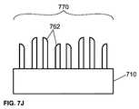
850と図7Jに示されているように、パターン−たとえば第1の減少したCD726と第1の減少した粗さを有する第1パターン722、及び、第2の減少したCD746と第2の減少した粗さを有する第2パターン742を含むマンドレルパターン750−は、1つ以上のエッチングプロセスを用いることによって除去される。その結果、パターンの側壁765に接した状態で残る材料層760の残りの部分762を含む最終パターン770が残される。その結果、最終パターン770は、第1パターン722と第2パターン742を起源とする四重パターンを含んで良い。1つ以上のエッチングプロセスは、湿式又は乾式エッチングプロセスの任意の組み合わせを含んで良い。乾式エッチングプロセスは乾式プラズマエッチングプロセス又は乾式非プラズマエッチングプロセスを含んで良い。一の実施例では、酸素を含むプロセス化合物で生成されるプラズマを用いた乾式プラズマエッチングプロセスが考えられる。 As shown in FIG. 850 and FIG. 7J, a pattern—eg, a
その後最終パターン770−材料層760の残りの部分762を含む−は、1つ以上のエッチングプロセスを用いることによって転写される。1つ以上のエッチングプロセスは、湿式又は乾式エッチングプロセスの任意の組み合わせを含んで良い。乾式エッチングプロセスは乾式プラズマエッチングプロセス又は乾式非プラズマエッチングプロセスを含んで良い。 Thereafter, the
第1CDスリム化プロセス、第1平滑化プロセス、第2CDスリム化プロセス、第2平滑化プロセス、硬化プロセス、第1リソグラフィプロセス、若しくは第2リソグラフィプロセス、又はこれら2つ以上の組み合わせについての少なくとも1つのプロセスパラメータは、第1パターンと第2パターンの破損を防止するように最適化されて良い。さらに第1CDスリム化プロセス、第1平滑化プロセス、第2CDスリム化プロセス、第2平滑化プロセス、硬化プロセス、第1リソグラフィプロセス、若しくは第2リソグラフィプロセス、又はこれら2つ以上の組み合わせについての少なくとも1つのプロセスパラメータは、硬化プロセスが施された第1パターン中の第1の減少したCDへの影響を最小限にしながら第2パターン中に第2の減少したCDを生成するように最適化されて良い。 At least one of the first CD slimming process, the first smoothing process, the second CD slimming process, the second smoothing process, the curing process, the first lithography process, the second lithography process, or a combination of two or more thereof The process parameters may be optimized to prevent damage to the first pattern and the second pattern. Further, at least one of the first CD slimming process, the first smoothing process, the second CD slimming process, the second smoothing process, the curing process, the first lithography process, the second lithography process, or a combination of two or more thereof Two process parameters are optimized to produce a second reduced CD in the second pattern while minimizing the impact on the first reduced CD in the first pattern subjected to the curing process good.
例として、第1パターンの第1CD及び/又は第2パターンの第2CDは、減少したCDと減少した粗さを有する第1パターンと第2パターンの最適印刷を実現するように調節されて良い。あるいはその代わりに例として、第1CDと第1の減少したCDとの間での減少量、第1粗さと第1の減少した粗さとの間での減少量、第2CDと第2の減少したCDとの間での減少量、及び/又は第2粗さと第2の減少した粗さとの間での減少量は、減少したCDと減少した粗さを有する第1パターンと第2パターンの最適印刷を実現するように調節されて良い。 As an example, the first CD of the first pattern and / or the second CD of the second pattern may be adjusted to achieve optimal printing of the first pattern and the second pattern with reduced CD and reduced roughness. Or alternatively, as an example, the amount of reduction between the first CD and the first reduced CD, the amount of reduction between the first roughness and the first reduced roughness, the second CD and the second reduction The amount of reduction between the CD and / or the amount of reduction between the second roughness and the second reduced roughness is the optimum of the first and second patterns with reduced CD and reduced roughness. It can be adjusted to achieve printing.
一の実施例では、第2CDスリム化プロセスは、第1パターン中の第1の減少したCDへの影響を最小限に抑制しながら、第2パターン中の第2の減少したCDを実現するように設計されて良い。たとえば第1リソグラフィプロセスと第2リソグラフィプロセスが実行されることで、実質的すなわち近似的に等しい第1CDと第2CDが印刷されて良い。その後、第1CDスリム化プロセスは第1CDを第1の減少したCDへ減少させ、第2CDスリム化プロセスは、第1の減少したCDへ影響しないように第2CDを第2の減少したCDへ減少させる。その結果第1の減少したCDと第2の減少したCDは実質的すなわち近似的に等しくなる。 In one embodiment, the second CD slimming process is adapted to achieve the second reduced CD in the second pattern while minimizing the impact on the first reduced CD in the first pattern. Can be designed to For example, a first lithographic process and a second lithographic process may be performed to print a first CD and a second CD that are substantially or approximately equal. The first CD slimming process then reduces the first CD to the first reduced CD, and the second CD slimming process reduces the second CD to the second reduced CD so as not to affect the first reduced CD. Let As a result, the first reduced CD and the second reduced CD are substantially or approximately equal.
他の実施例では、第2CDスリム化プロセスは、第1の減少したCDと第2の減少したCDの両方の減少を実現するように設計されて良い。たとえば第1リソグラフィプロセスと第2リソグラフィプロセスが実行されることで、第1CDと第2CDが実現されて良い。前記第1CDは、前記第2CDよりも大きく印刷される。それに加えてたとえば第1CDは、前記第2CDよりも最大で約5%大きく印刷される。それに加えてたとえば第1CDは、前記第2CDよりも最大で約10%大きく印刷される。それに加えてたとえば第1CDは、前記第2CDよりも最大で約15%大きく印刷される。それに加えてたとえば第1CDは、前記第2CDよりも最大で約25%大きく印刷される。それに加えてたとえば第1CDは、前記第2CDよりも約25%〜約50%大きく印刷される。それに加えてたとえば第1CDは、前記第2CDよりも約50%〜約75%大きく印刷される。その後、第1CDスリム化プロセスは第1CDを第1の減少したCDへ減少させ、第2CDスリム化プロセスは、第1の減少したCDを第3の減少したCDへさらに減少させながら、第2CDを第2の減少したCDへ減少させる。その結果第3の減少したCDと第2の減少したCDは実質的すなわち近似的に等しくなる。 In other embodiments, the second CD slimming process may be designed to achieve a reduction of both the first reduced CD and the second reduced CD. For example, the first CD and the second CD may be realized by executing the first lithography process and the second lithography process. The first CD is printed larger than the second CD. In addition, for example, the first CD is printed up to about 5% larger than the second CD. In addition, for example, the first CD is printed about 10% larger than the second CD. In addition, for example, the first CD is printed by about 15% larger than the second CD. In addition, for example, the first CD is printed up to about 25% larger than the second CD. In addition, for example, the first CD is printed about 25% to about 50% larger than the second CD. In addition, for example, the first CD is printed about 50% to about 75% larger than the second CD. The first CD slimming process then reduces the first CD to the first reduced CD, and the second CD slimming process further reduces the first CD to the third reduced CD, while reducing the second CD. Reduce to the second reduced CD. As a result, the third reduced CD and the second reduced CD are substantially or approximately equal.
たとえ本発明のある典型的実施例のみが詳細に説明されたとしても、当業者は、本発明の新規な教示及び利点からほとんど逸脱することなく、多くの修正型が可能であることをすぐに理解する。従って多くの係る修正型は、本発明の技術的範囲内に含まれるものと解される。 Even if only certain exemplary embodiments of the present invention are described in detail, those skilled in the art will readily appreciate that many modifications are possible without departing substantially from the novel teachings and advantages of the present invention. to understand. Accordingly, it is understood that many such modified types are included within the technical scope of the present invention.
Claims (20)
Translated fromJapanese基板上に放射線感受性材料層を形成する工程;及び、
リソグラフィプロセスを用いることによって前記放射線感受性材料層内にパターンを準備する工程であって、前記パターンは、限界寸法(CD)及び粗さによって特徴付けられる、工程;
前記放射線感受性材料層内にパターンを準備する工程に続いて、CDスリム化プロセスを実行することで前記CDを減少したCDにする工程;及び、
蒸気平滑化プロセスを実行することで前記粗さを減少した粗さにする工程;
を有する方法。A method for patterning a substrate comprising:
Forming a radiation sensitive material layer on the substrate; and
Providing a pattern in the radiation sensitive material layer by using a lithography process, wherein the pattern is characterized by critical dimension (CD) and roughness;
Following the step of preparing a pattern in the radiation sensitive material layer, performing a CD slimming process to reduce the CD to a reduced CD; and
Performing the steam smoothing process to reduce the roughness to a reduced roughness;
Having a method.
10%を超える粗さの減少を実現する工程であって、前記粗さの減少は、前記平滑化前の処理粗さに対する前記平滑化処理前の粗さと前記平滑化後の粗さとの差のパーセント表示の比として測定される、工程;
をさらに含む、請求項1に記載の方法。Determining the roughness before smoothing evaluated immediately before the steam smoothing process and evaluating the roughness by determining the roughness after smoothing evaluated immediately after the steam smoothing process; ;as well as,
A reduction in roughness exceeding 10%, wherein the reduction in roughness is the difference between the roughness before the smoothing and the roughness after the smoothing with respect to the roughness before the smoothing. A process, measured as a percentage ratio;
The method of claim 1, further comprising:
30%を超える粗さの減少を実現する工程であって、前記粗さの減少は、前記平滑化前の処理粗さに対する前記平滑化処理前の粗さと前記平滑化後の粗さとの差のパーセント表示の比として測定される、工程;
をさらに含む、請求項1に記載の方法。Determining the roughness before smoothing evaluated immediately before the steam smoothing process and evaluating the roughness by determining the roughness after smoothing evaluated immediately after the steam smoothing process; ;as well as,
A reduction in roughness exceeding 30%, wherein the reduction in roughness is a difference between a roughness before the smoothing and a roughness after the smoothing with respect to the processing roughness before the smoothing. A process, measured as a percentage ratio;
The method of claim 1, further comprising:
30℃を超える熱源像温度に加熱された現像溶液を前記基板上に供給する工程;
酸を含む処理化合物によって前記基板を処理する工程;
前記酸が前記パターンへ入り込むように拡散するように前記基板をベーキングする工程;及び、
前記基板上に他の現像溶液を供給する工程;
を有する、請求項1に記載の方法。The CD slimming process is:
Supplying a developing solution heated to a heat source image temperature exceeding 30 ° C. onto the substrate;
Treating the substrate with a treatment compound comprising an acid;
Baking the substrate such that the acid diffuses into the pattern; and
Supplying another developer solution onto the substrate;
The method of claim 1, comprising:
前記放射線感受性材料層中の減少したCDを有するパターン上に放射線感受性材料の第2層を形成する工程;
第2リソグラフィプロセスを用いることによって、第2CDと第2粗さによって特徴付けられる第2パターンを前記放射線感受性材料の第2層中に準備する工程;
前記第2パターンの準備後に、第2CDスリム化プロセスを実行することで、前記第2CDを第2の減少したCDにする工程;及び、
前記第2パターンの準備後に、第2蒸気平滑化化プロセスを実行することで、前記第2粗さを第2の減少した粗さにする工程;
をさらに有する、請求項1に記載の方法。Curing the pattern with reduced CD in the radiation sensitive material layer by using a curing process;
Forming a second layer of radiation sensitive material on the pattern having reduced CD in the radiation sensitive material layer;
Providing a second pattern characterized by a second CD and a second roughness in the second layer of the radiation sensitive material by using a second lithography process;
After preparing the second pattern, performing a second CD slimming process to make the second CD a second reduced CD; and
After preparing the second pattern, performing a second steam smoothing process to reduce the second roughness to a second reduced roughness;
The method of claim 1, further comprising:
前記硬化プロセスを用いることによって放射線感受性材料層中で前記パターンを硬化する工程は、前記放射線感受性材料層をベーキングすることで、前記減少したCDを有する前記パターンを熱的に硬化して保持する工程を含む、
請求項10に記載の方法。The radiation sensitive material layer comprises a thermally curable cured resist; and
The step of curing the pattern in the radiation sensitive material layer by using the curing process includes thermally curing and holding the pattern having the reduced CD by baking the radiation sensitive material layer. including,
The method according to claim 10.
前記硬化プロセスを用いることによって前記放射線感受性材料層をEM放射線に曝露することで、前記減少したCDを有する前記パターンを放射線によって硬化して保持する工程を含む、
請求項10に記載の方法。The radiation sensitive material layer comprises a hardened resist curable by electromagnetic (EM) radiation; and
Exposing the radiation sensitive material layer to EM radiation by using the curing process to cure and retain the pattern with the reduced CD by radiation;
The method according to claim 10.
前記硬化プロセスを用いることによって前記放射線感受性材料層中の前記パターンを硬化する工程は、化学硬化材料を前記放射線感受性材料層に塗布する工程;
前記化学硬化材料と前記放射線感受性材料層とを反応させることで、前記減少したCDを有する前記パターンを化学的に硬化して保持する工程を含む、
請求項11に記載の方法。The radiation sensitive material layer comprises a chemically curable cured resist; and
Curing the pattern in the radiation sensitive material layer by using the curing process, applying a chemically cured material to the radiation sensitive material layer;
Reacting the chemically hardened material with the radiation sensitive material layer to chemically harden and hold the pattern with the reduced CD,
The method of claim 11.
Applications Claiming Priority (3)
| Application Number | Priority Date | Filing Date | Title |
|---|---|---|---|
| US13/342,313US8647817B2 (en) | 2012-01-03 | 2012-01-03 | Vapor treatment process for pattern smoothing and inline critical dimension slimming |
| US13/342,313 | 2012-01-03 | ||
| PCT/US2012/069082WO2013103482A1 (en) | 2012-01-03 | 2012-12-12 | Vapor treatment process for pattern smoothing and inline critical dimension slimming |
Publications (2)
| Publication Number | Publication Date |
|---|---|
| JP2015508574Atrue JP2015508574A (en) | 2015-03-19 |
| JP5851052B2 JP5851052B2 (en) | 2016-02-03 |
Family
ID=48695066
Family Applications (1)
| Application Number | Title | Priority Date | Filing Date |
|---|---|---|---|
| JP2014551251AActiveJP5851052B2 (en) | 2012-01-03 | 2012-12-12 | Steam treatment process for pattern smoothing and slimming of inline critical dimensions |
Country Status (5)
| Country | Link |
|---|---|
| US (1) | US8647817B2 (en) |
| JP (1) | JP5851052B2 (en) |
| KR (1) | KR101625782B1 (en) |
| TW (1) | TWI505326B (en) |
| WO (1) | WO2013103482A1 (en) |
Cited By (1)
| Publication number | Priority date | Publication date | Assignee | Title |
|---|---|---|---|---|
| JP2019517137A (en)* | 2016-05-13 | 2019-06-20 | 東京エレクトロン株式会社 | Critical dimension control using light agent |
Families Citing this family (19)
| Publication number | Priority date | Publication date | Assignee | Title |
|---|---|---|---|---|
| US8764999B2 (en)* | 2010-11-23 | 2014-07-01 | Tokyo Electron Limited | Sidewall image transfer pitch doubling and inline critical dimension slimming |
| US9097977B2 (en)* | 2012-05-15 | 2015-08-04 | Tokyo Electron Limited | Process sequence for reducing pattern roughness and deformity |
| US8986562B2 (en) | 2013-08-07 | 2015-03-24 | Ultratech, Inc. | Methods of laser processing photoresist in a gaseous environment |
| US9653319B2 (en) | 2013-11-08 | 2017-05-16 | Tokyo Electron Limited | Method for using post-processing methods for accelerating EUV lithography |
| KR101888287B1 (en)* | 2014-01-27 | 2018-08-13 | 도쿄엘렉트론가부시키가이샤 | System and method for shifting critical dimensions of patterned films |
| JP6758575B2 (en) | 2014-02-24 | 2020-09-23 | 東京エレクトロン株式会社 | Photosensitive Chemical Amplification Resist Methods and Techniques Using Chemicals and Processes |
| KR102233577B1 (en) | 2014-02-25 | 2021-03-30 | 삼성전자주식회사 | Method for forming patterns of a semiconductor device |
| KR102402422B1 (en) | 2014-02-25 | 2022-05-25 | 도쿄엘렉트론가부시키가이샤 | Chemical amplification methods and techniques for developable bottom anti-reflective coatings and dyed implant resists |
| JP2016206449A (en)* | 2015-04-23 | 2016-12-08 | 株式会社東芝 | Pattern formation method |
| JP2016213475A (en)* | 2015-05-13 | 2016-12-15 | 東京エレクトロン株式会社 | Extreme ultraviolet sensitivity reduction using shrink and growth method |
| JP6236481B2 (en)* | 2016-02-17 | 2017-11-22 | 東京エレクトロン株式会社 | Pattern formation method |
| US10048594B2 (en) | 2016-02-19 | 2018-08-14 | Tokyo Electron Limited | Photo-sensitized chemically amplified resist (PS-CAR) model calibration |
| US10429745B2 (en) | 2016-02-19 | 2019-10-01 | Osaka University | Photo-sensitized chemically amplified resist (PS-CAR) simulation |
| WO2017197279A1 (en) | 2016-05-13 | 2017-11-16 | Tokyo Electron Limited | Critical dimension control by use of photo-sensitized chemicals or photo-sensitized chemically amplified resist |
| US11355342B2 (en)* | 2019-06-13 | 2022-06-07 | Nanya Technology Corporation | Semiconductor device with reduced critical dimensions and method of manufacturing the same |
| WO2021034567A1 (en) | 2019-08-16 | 2021-02-25 | Tokyo Electron Limited | Method and process for stochastic driven defectivity healing |
| US12130559B2 (en) | 2022-01-26 | 2024-10-29 | Nanya Technology Corporation | Method for measuring critical dimension |
| TWI803337B (en)* | 2022-01-26 | 2023-05-21 | 南亞科技股份有限公司 | Method for measuring critical dimension |
| US12117733B2 (en) | 2022-01-26 | 2024-10-15 | Nanya Technology Corporation | Method for measuring critical dimension |
Citations (11)
| Publication number | Priority date | Publication date | Assignee | Title |
|---|---|---|---|---|
| JP2005019969A (en)* | 2003-06-06 | 2005-01-20 | Tokyo Electron Ltd | Method of improving surface roughness of processed film of substrate, and processor for substrate |
| JP2005523177A (en)* | 2002-04-17 | 2005-08-04 | ストラッタシス, インコーポレイテッド | A smoothing method for layered laminate modeling. |
| JP2007522673A (en)* | 2004-02-13 | 2007-08-09 | フリースケール セミコンダクター インコーポレイテッド | Method for forming a semiconductor device using a treated photoresist |
| US20090155731A1 (en)* | 2007-12-14 | 2009-06-18 | Tokyo Electron Limited | Method and system for reducing line edge roughness during pattern etching |
| JP2009147261A (en)* | 2007-12-18 | 2009-07-02 | Tokyo Electron Ltd | Substrate processing apparatus |
| US20090214985A1 (en)* | 2008-02-27 | 2009-08-27 | Tokyo Electron Limited | Method for reducing surface defects on patterned resist features |
| JP2009230106A (en)* | 2008-02-28 | 2009-10-08 | Tokyo Electron Ltd | Method of manufacturing semiconductor device and resist coating-developing system |
| JP2010267880A (en)* | 2009-05-15 | 2010-11-25 | Tokyo Electron Ltd | Resist pattern slimming treatment method |
| US20110014790A1 (en)* | 2009-07-20 | 2011-01-20 | Globalfoundries Inc. | Methods for fabricating semiconductor devices |
| US20110111596A1 (en)* | 2009-11-06 | 2011-05-12 | International Business Machine Corporation | Sidewall Image Transfer Using the Lithographic Stack as the Mandrel |
| JP2011197150A (en)* | 2010-03-17 | 2011-10-06 | Jsr Corp | Radiation-sensitive composition and resist pattern forming method using the same |
Family Cites Families (9)
| Publication number | Priority date | Publication date | Assignee | Title |
|---|---|---|---|---|
| US5096802A (en)* | 1990-11-09 | 1992-03-17 | Hewlett-Packard Company | Holes and spaces shrinkage |
| US6582891B1 (en) | 1999-12-02 | 2003-06-24 | Axcelis Technologies, Inc. | Process for reducing edge roughness in patterned photoresist |
| US7135419B2 (en) | 2002-09-16 | 2006-11-14 | Intel Corporation | Line edge roughness reduction |
| US7405032B1 (en) | 2003-08-21 | 2008-07-29 | Advanced Micro Devices, Inc. | Combination of non-lithographic shrink techniques and trim process for gate formation and line-edge roughness reduction |
| JP2008171911A (en) | 2007-01-10 | 2008-07-24 | Tokyo Electron Ltd | Method and system for evaluating roughness |
| US20090108486A1 (en) | 2007-10-26 | 2009-04-30 | Sergey Babin | Method and apparatus for smoothening rough edges of lithographic patterns |
| US8389206B2 (en) | 2009-09-22 | 2013-03-05 | Tokyo Electron Limited | High normality solution for removing freeze material in lithographic applications |
| US8338086B2 (en) | 2010-03-31 | 2012-12-25 | Tokyo Electron Limited | Method of slimming radiation-sensitive material lines in lithographic applications |
| US8435728B2 (en) | 2010-03-31 | 2013-05-07 | Tokyo Electron Limited | Method of slimming radiation-sensitive material lines in lithographic applications |
- 2012
- 2012-01-03USUS13/342,313patent/US8647817B2/enactiveActive
- 2012-12-12KRKR1020147021732Apatent/KR101625782B1/enactiveActive
- 2012-12-12WOPCT/US2012/069082patent/WO2013103482A1/enactiveApplication Filing
- 2012-12-12JPJP2014551251Apatent/JP5851052B2/enactiveActive
- 2012-12-24TWTW101149512Apatent/TWI505326B/enactive
Patent Citations (11)
| Publication number | Priority date | Publication date | Assignee | Title |
|---|---|---|---|---|
| JP2005523177A (en)* | 2002-04-17 | 2005-08-04 | ストラッタシス, インコーポレイテッド | A smoothing method for layered laminate modeling. |
| JP2005019969A (en)* | 2003-06-06 | 2005-01-20 | Tokyo Electron Ltd | Method of improving surface roughness of processed film of substrate, and processor for substrate |
| JP2007522673A (en)* | 2004-02-13 | 2007-08-09 | フリースケール セミコンダクター インコーポレイテッド | Method for forming a semiconductor device using a treated photoresist |
| US20090155731A1 (en)* | 2007-12-14 | 2009-06-18 | Tokyo Electron Limited | Method and system for reducing line edge roughness during pattern etching |
| JP2009147261A (en)* | 2007-12-18 | 2009-07-02 | Tokyo Electron Ltd | Substrate processing apparatus |
| US20090214985A1 (en)* | 2008-02-27 | 2009-08-27 | Tokyo Electron Limited | Method for reducing surface defects on patterned resist features |
| JP2009230106A (en)* | 2008-02-28 | 2009-10-08 | Tokyo Electron Ltd | Method of manufacturing semiconductor device and resist coating-developing system |
| JP2010267880A (en)* | 2009-05-15 | 2010-11-25 | Tokyo Electron Ltd | Resist pattern slimming treatment method |
| US20110014790A1 (en)* | 2009-07-20 | 2011-01-20 | Globalfoundries Inc. | Methods for fabricating semiconductor devices |
| US20110111596A1 (en)* | 2009-11-06 | 2011-05-12 | International Business Machine Corporation | Sidewall Image Transfer Using the Lithographic Stack as the Mandrel |
| JP2011197150A (en)* | 2010-03-17 | 2011-10-06 | Jsr Corp | Radiation-sensitive composition and resist pattern forming method using the same |
Cited By (1)
| Publication number | Priority date | Publication date | Assignee | Title |
|---|---|---|---|---|
| JP2019517137A (en)* | 2016-05-13 | 2019-06-20 | 東京エレクトロン株式会社 | Critical dimension control using light agent |
Also Published As
| Publication number | Publication date |
|---|---|
| WO2013103482A1 (en) | 2013-07-11 |
| TWI505326B (en) | 2015-10-21 |
| JP5851052B2 (en) | 2016-02-03 |
| TW201342425A (en) | 2013-10-16 |
| KR101625782B1 (en) | 2016-05-30 |
| KR20140110043A (en) | 2014-09-16 |
| US8647817B2 (en) | 2014-02-11 |
| US20130171571A1 (en) | 2013-07-04 |
Similar Documents
| Publication | Publication Date | Title |
|---|---|---|
| JP5851052B2 (en) | Steam treatment process for pattern smoothing and slimming of inline critical dimensions | |
| JP6045504B2 (en) | Sidewall image transfer pitch doubling and inline critical dimension slimming | |
| TWI483079B (en) | Pattern formation method | |
| JP5120983B2 (en) | Spacer lithography | |
| CN103280403B (en) | Manufacturing method for dual gate oxide device | |
| KR101752948B1 (en) | Method for high aspect ratio patterning in spin-on layer | |
| US7851139B2 (en) | Pattern forming method | |
| TWI864232B (en) | Substrate processing method and substrate processing system | |
| KR101745810B1 (en) | Euv resist sensitivity reduction | |
| US8138059B2 (en) | Semiconductor device manufacturing method | |
| KR100645835B1 (en) | Method of forming photoresist pattern of semiconductor device | |
| CN105988284A (en) | Double-mask self-aligning patterning method | |
| JP2000100689A (en) | Photolithography using gas phase pretreatment |
Legal Events
| Date | Code | Title | Description |
|---|---|---|---|
| A977 | Report on retrieval | Free format text:JAPANESE INTERMEDIATE CODE: A971007 Effective date:20150727 | |
| A131 | Notification of reasons for refusal | Free format text:JAPANESE INTERMEDIATE CODE: A131 Effective date:20150804 | |
| A521 | Request for written amendment filed | Free format text:JAPANESE INTERMEDIATE CODE: A523 Effective date:20150928 | |
| TRDD | Decision of grant or rejection written | ||
| A01 | Written decision to grant a patent or to grant a registration (utility model) | Free format text:JAPANESE INTERMEDIATE CODE: A01 Effective date:20151104 | |
| A61 | First payment of annual fees (during grant procedure) | Free format text:JAPANESE INTERMEDIATE CODE: A61 Effective date:20151201 | |
| R150 | Certificate of patent or registration of utility model | Ref document number:5851052 Country of ref document:JP Free format text:JAPANESE INTERMEDIATE CODE: R150 | |
| R250 | Receipt of annual fees | Free format text:JAPANESE INTERMEDIATE CODE: R250 | |
| R250 | Receipt of annual fees | Free format text:JAPANESE INTERMEDIATE CODE: R250 | |
| R250 | Receipt of annual fees | Free format text:JAPANESE INTERMEDIATE CODE: R250 | |
| R250 | Receipt of annual fees | Free format text:JAPANESE INTERMEDIATE CODE: R250 | |
| R250 | Receipt of annual fees | Free format text:JAPANESE INTERMEDIATE CODE: R250 | |
| R250 | Receipt of annual fees | Free format text:JAPANESE INTERMEDIATE CODE: R250 | |
| R250 | Receipt of annual fees | Free format text:JAPANESE INTERMEDIATE CODE: R250 |