JP2015502657A - Epitaxial film growth in retrograde wells for semiconductor devices. - Google Patents
Epitaxial film growth in retrograde wells for semiconductor devices.Download PDFInfo
- Publication number
- JP2015502657A JP2015502657AJP2014540096AJP2014540096AJP2015502657AJP 2015502657 AJP2015502657 AJP 2015502657AJP 2014540096 AJP2014540096 AJP 2014540096AJP 2014540096 AJP2014540096 AJP 2014540096AJP 2015502657 AJP2015502657 AJP 2015502657A
- Authority
- JP
- Japan
- Prior art keywords
- trenches
- fin structures
- dislocation density
- substrate
- aspect ratio
- Prior art date
- Legal status (The legal status is an assumption and is not a legal conclusion. Google has not performed a legal analysis and makes no representation as to the accuracy of the status listed.)
- Pending
Links
- 239000004065semiconductorSubstances0.000titleclaimsabstractdescription18
- 238000000034methodMethods0.000claimsabstractdescription76
- 239000000463materialSubstances0.000claimsabstractdescription32
- 239000000758substrateSubstances0.000claimsabstractdescription29
- 150000001875compoundsChemical class0.000claimsabstractdescription18
- 229910052732germaniumInorganic materials0.000claimsabstractdescription14
- GNPVGFCGXDBREM-UHFFFAOYSA-Ngermanium atomChemical compound[Ge]GNPVGFCGXDBREM-UHFFFAOYSA-N0.000claimsabstractdescription14
- 238000004519manufacturing processMethods0.000claimsabstractdescription14
- 239000000203mixtureSubstances0.000claimsabstractdescription13
- 238000005530etchingMethods0.000claimsdescription15
- 230000005669field effectEffects0.000claimsdescription7
- 229910001218Gallium arsenideInorganic materials0.000claimsdescription4
- 238000000151depositionMethods0.000claimsdescription4
- 230000000873masking effectEffects0.000claimsdescription2
- 238000000059patterningMethods0.000claims1
- 239000003989dielectric materialSubstances0.000abstractdescription6
- 239000010410layerSubstances0.000description37
- 208000012868OvergrowthDiseases0.000description12
- XUIMIQQOPSSXEZ-UHFFFAOYSA-NSiliconChemical compound[Si]XUIMIQQOPSSXEZ-UHFFFAOYSA-N0.000description12
- 229910052710siliconInorganic materials0.000description12
- 239000010703siliconSubstances0.000description11
- 239000000126substanceSubstances0.000description9
- 239000013078crystalSubstances0.000description8
- VYPSYNLAJGMNEJ-UHFFFAOYSA-NSilicium dioxideChemical compoundO=[Si]=OVYPSYNLAJGMNEJ-UHFFFAOYSA-N0.000description6
- 239000007789gasSubstances0.000description5
- 238000001020plasma etchingMethods0.000description5
- 238000000708deep reactive-ion etchingMethods0.000description4
- JBRZTFJDHDCESZ-UHFFFAOYSA-NAsGaChemical compound[As]#[Ga]JBRZTFJDHDCESZ-UHFFFAOYSA-N0.000description3
- GPXJNWSHGFTCBW-UHFFFAOYSA-NIndium phosphideChemical compound[In]#PGPXJNWSHGFTCBW-UHFFFAOYSA-N0.000description3
- 238000007796conventional methodMethods0.000description3
- 230000007423decreaseEffects0.000description3
- 229920002120photoresistant polymerPolymers0.000description3
- 238000005498polishingMethods0.000description3
- IJGRMHOSHXDMSA-UHFFFAOYSA-NAtomic nitrogenChemical compoundN#NIJGRMHOSHXDMSA-UHFFFAOYSA-N0.000description2
- 230000000295complement effectEffects0.000description2
- 238000011109contaminationMethods0.000description2
- 230000008021depositionEffects0.000description2
- 238000010586diagramMethods0.000description2
- 230000010354integrationEffects0.000description2
- 229910052751metalInorganic materials0.000description2
- 239000002184metalSubstances0.000description2
- 229910052760oxygenInorganic materials0.000description2
- 239000001301oxygenSubstances0.000description2
- HBMJWWWQQXIZIP-UHFFFAOYSA-Nsilicon carbideChemical compound[Si+]#[C-]HBMJWWWQQXIZIP-UHFFFAOYSA-N0.000description2
- 229910010271silicon carbideInorganic materials0.000description2
- 239000000377silicon dioxideSubstances0.000description2
- 235000012239silicon dioxideNutrition0.000description2
- LIVNPJMFVYWSIS-UHFFFAOYSA-Nsilicon monoxideChemical compound[Si-]#[O+]LIVNPJMFVYWSIS-UHFFFAOYSA-N0.000description2
- 239000002210silicon-based materialSubstances0.000description2
- 239000010936titaniumSubstances0.000description2
- 229910018182Al—CuInorganic materials0.000description1
- OKTJSMMVPCPJKN-UHFFFAOYSA-NCarbonChemical compound[C]OKTJSMMVPCPJKN-UHFFFAOYSA-N0.000description1
- 229910000881Cu alloyInorganic materials0.000description1
- 229910000673Indium arsenideInorganic materials0.000description1
- 229910019093NaOClInorganic materials0.000description1
- 229910052581Si3N4Inorganic materials0.000description1
- 229910004298SiO 2Inorganic materials0.000description1
- ATJFFYVFTNAWJD-UHFFFAOYSA-NTinChemical compound[Sn]ATJFFYVFTNAWJD-UHFFFAOYSA-N0.000description1
- RTAQQCXQSZGOHL-UHFFFAOYSA-NTitaniumChemical compound[Ti]RTAQQCXQSZGOHL-UHFFFAOYSA-N0.000description1
- NRTOMJZYCJJWKI-UHFFFAOYSA-NTitanium nitrideChemical compound[Ti]#NNRTOMJZYCJJWKI-UHFFFAOYSA-N0.000description1
- 229910052782aluminiumInorganic materials0.000description1
- XAGFODPZIPBFFR-UHFFFAOYSA-NaluminiumChemical compound[Al]XAGFODPZIPBFFR-UHFFFAOYSA-N0.000description1
- WPPDFTBPZNZZRP-UHFFFAOYSA-Naluminum copperChemical compound[Al].[Cu]WPPDFTBPZNZZRP-UHFFFAOYSA-N0.000description1
- 229910003481amorphous carbonInorganic materials0.000description1
- QVGXLLKOCUKJST-UHFFFAOYSA-Natomic oxygenChemical compound[O]QVGXLLKOCUKJST-UHFFFAOYSA-N0.000description1
- 230000005540biological transmissionEffects0.000description1
- 230000015572biosynthetic processEffects0.000description1
- 229910052799carbonInorganic materials0.000description1
- 238000005229chemical vapour depositionMethods0.000description1
- 239000008119colloidal silicaSubstances0.000description1
- 238000002425crystallisationMethods0.000description1
- 230000007547defectEffects0.000description1
- 238000005137deposition processMethods0.000description1
- 230000005684electric fieldEffects0.000description1
- 238000005265energy consumptionMethods0.000description1
- NBVXSUQYWXRMNV-UHFFFAOYSA-NfluoromethaneChemical compoundFCNBVXSUQYWXRMNV-UHFFFAOYSA-N0.000description1
- 150000004820halidesChemical class0.000description1
- 229910052736halogenInorganic materials0.000description1
- 150000002367halogensChemical class0.000description1
- 229910052739hydrogenInorganic materials0.000description1
- 239000001257hydrogenSubstances0.000description1
- 150000002431hydrogenChemical class0.000description1
- WPYVAWXEWQSOGY-UHFFFAOYSA-Nindium antimonideChemical compound[Sb]#[In]WPYVAWXEWQSOGY-UHFFFAOYSA-N0.000description1
- RPQDHPTXJYYUPQ-UHFFFAOYSA-Nindium arsenideChemical compound[In]#[As]RPQDHPTXJYYUPQ-UHFFFAOYSA-N0.000description1
- 239000011261inert gasSubstances0.000description1
- 150000002500ionsChemical class0.000description1
- 230000000116mitigating effectEffects0.000description1
- 238000012986modificationMethods0.000description1
- 230000004048modificationEffects0.000description1
- 229910052757nitrogenInorganic materials0.000description1
- 229910052756noble gasInorganic materials0.000description1
- 230000000737periodic effectEffects0.000description1
- 238000005268plasma chemical vapour depositionMethods0.000description1
- 238000000623plasma-assisted chemical vapour depositionMethods0.000description1
- 230000000644propagated effectEffects0.000description1
- 239000011241protective layerSubstances0.000description1
- 230000003252repetitive effectEffects0.000description1
- 238000005389semiconductor device fabricationMethods0.000description1
- HQVNEWCFYHHQES-UHFFFAOYSA-Nsilicon nitrideChemical compoundN12[Si]34N5[Si]62N3[Si]51N64HQVNEWCFYHHQES-UHFFFAOYSA-N0.000description1
- 229910052814silicon oxideInorganic materials0.000description1
- 239000002356single layerSubstances0.000description1
- 239000002002slurrySubstances0.000description1
- SUKJFIGYRHOWBL-UHFFFAOYSA-Nsodium hypochloriteChemical compound[Na+].Cl[O-]SUKJFIGYRHOWBL-UHFFFAOYSA-N0.000description1
- 229910052715tantalumInorganic materials0.000description1
- GUVRBAGPIYLISA-UHFFFAOYSA-Ntantalum atomChemical compound[Ta]GUVRBAGPIYLISA-UHFFFAOYSA-N0.000description1
- MZLGASXMSKOWSE-UHFFFAOYSA-Ntantalum nitrideChemical compound[Ta]#NMZLGASXMSKOWSE-UHFFFAOYSA-N0.000description1
- 229910052719titaniumInorganic materials0.000description1
- 238000007740vapor depositionMethods0.000description1
Images


Landscapes
- Recrystallisation Techniques (AREA)
- Insulated Gate Type Field-Effect Transistor (AREA)
Abstract
Translated fromJapaneseDescription
Translated fromJapanese本発明は、半導体デバイスの製造方法に関し、より具体的には、半導体デバイスの部位内の転位密度を減少させる製造方法に関する。 The present invention relates to a method for manufacturing a semiconductor device, and more specifically to a method for reducing a dislocation density in a portion of a semiconductor device.
相補型金属−酸化物−半導体(“CMOS”)は、マイクロプロセッサ、マイクロコントローラ、及び他の論理回路内において用いられる集積回路の製造に通常用いられる。CMOSデバイスは通常、論理ゲートとデジタル回路を構成する電界効果型トランジスタ(“FET”)の相補的で対称的な対−具体的にはn型及びp型金属−酸化物−半導体電界効果型トランジスタ(“MOSFET”)−を有する。 Complementary metal-oxide-semiconductors ("CMOS") are commonly used in the manufacture of integrated circuits used in microprocessors, microcontrollers, and other logic circuits. CMOS devices are typically complementary and symmetrical pairs of field effect transistors (“FETs”) that make up logic gates and digital circuits—specifically, n-type and p-type metal-oxide-semiconductor field-effect transistors. (“MOSFET”) −.
使用時、2つのn型半導体領域(又はソース及びドレインとも呼ばれる)はゲートによって電気的に結合されている。一部のデバイスでは、狭いチャネル−FIN構造とも呼ばれる−が、ソースとドレインとの間に存在する。誘電材料が、ゲートからFIN構造を隔離する。 In use, two n-type semiconductor regions (also called sources and drains) are electrically coupled by a gate. In some devices, a narrow channel—also called a FIN structure—is present between the source and drain. A dielectric material isolates the FIN structure from the gate.
CMOSデバイスを機能させる方法は、電子の移動度、すなわち電子が電場によって引き込まれるときに、如何に迅速に材料中を移動するかである。たとえばFIN構造に沿って電子の移動度が増大することで、デバイスの速度を落とすことなくデバイスのエネルギー消費を劇的に減少させることができる。FIN構造並びに他の構成要素にIII-V族化合物(たとえばInAs及びInSb)及び/又はゲルマニウムを用いるデバイスは、所望の程度に電子移動度を増大させることが可能であることを示してきた。 The way to make a CMOS device work is the mobility of the electrons, ie how quickly they move through the material as they are drawn by the electric field. For example, increasing electron mobility along the FIN structure can dramatically reduce device energy consumption without slowing the device. Devices using III-V compounds (eg, InAs and InSb) and / or germanium in the FIN structure and other components have been shown to be able to increase electron mobility to the desired extent.
しかしIII-V族化合物及び/又はゲルマニウムの従来のCMOSデバイスへの統合は、従来の製造方法を用いては実現できない。従来の方法でシリコン及び/若しくは誘電材料(たとえば二酸化シリコン)上にIII-V族化合物及び/又はゲルマニウムを堆積する間に、格子不整合が生成される。格子不整合は転位を生成する。転位は、結晶構造の成長中に生成される結晶学上の欠陥で、最終的にはその結晶の特性−電子移動度を含む−に影響を及ぼす。換言すると、誘電材料に隣接する結晶のヘテロエピタキシャル成長は、少なくとも一の格子面内の結晶表面上に張力を生成する。一の面内での一の転位の存在は、隣接する格子面に伝播されうる。その結果転位が永続して、電子移動度がさらに低下する。隣接する格子面のさらなる歪みを緩和する一の既知である従来方法はアスペクト比トラッピング(“ART”)である。ART堆積処理は、ある部位の横方向に延びて閉じこめる側壁での転位を捕獲するように構成される反復的な堆積−結晶化の二段階処理である。所謂緩衝層が、成長サイクル間での格子不整合を緩和するのに用いられて良い。 However, the integration of III-V compounds and / or germanium into conventional CMOS devices cannot be achieved using conventional manufacturing methods. Lattice mismatch is created during the deposition of III-V compounds and / or germanium on silicon and / or dielectric materials (eg, silicon dioxide) in a conventional manner. Lattice mismatch generates dislocations. Dislocations are crystallographic defects created during the growth of a crystal structure and ultimately affect the properties of the crystal-including electron mobility. In other words, heteroepitaxial growth of crystals adjacent to the dielectric material creates tension on the crystal surface in at least one lattice plane. The presence of one dislocation in one plane can be propagated to the adjacent lattice plane. As a result, dislocation persists and the electron mobility further decreases. One known conventional method of mitigating further distortion of adjacent grating planes is aspect ratio trapping (“ART”). The ART deposition process is a repetitive deposition-crystallization two-step process that is configured to capture dislocations in the laterally extending and confining sidewalls of a site. So-called buffer layers may be used to mitigate lattice mismatch between growth cycles.
しかし多数の転位がCMOS製造における問題として残されている。よって結果として得られる構造の構造上の耐久性を増大させる、誘電材料上でのIII-V族化合物及び/又はゲルマニウムのヘテロエピタキシャル成長方法が必要とされる。 However, many dislocations remain as problems in CMOS manufacturing. Thus, there is a need for a method of heteroepitaxial growth of III-V compounds and / or germanium on dielectric materials that increases the structural durability of the resulting structure.
本発明は、III-V族化合物及び/又はゲルマニウムをシリコン系基板上に統合する既知の従来方法の上述の問題及び他の欠点や課題等を解決する。本発明はある実施例に関連づけて説明されるが、本発明はこれらの実施例に限定されない。対照的に本発明は、本発明の技術的範囲内に含まれうるすべての代替型、修正型、及び均等型を含む。 The present invention solves the above-mentioned problems and other drawbacks and problems of known conventional methods for integrating III-V compounds and / or germanium on silicon-based substrates. While the invention will be described in connection with certain embodiments, the invention is not limited to these embodiments. In contrast, the present invention includes all alternatives, modifications, and equivalents that may be included within the scope of the present invention.
本発明の一の実施例によると、半導体デバイスの製造方法は、上に誘電層とマスク層を有する基板を供する工程を有する。前記マスク層はパターニング及び現像される。その結果複数のトレンチが、レトログレードエッチングプロセスによって生成されうる。前記複数のトレンチには続いて、アスペクト比トラッピングを用いた材料のヘテロエピタキシャル成長によって前記材料が過充填される。前記材料は、ゲルマニウム、III-V族化合物、又は上記2つ以上の混合物のうちの少なくとも1つを含む。続いて前記の過充填された複数のトレンチは平坦化される。 According to one embodiment of the present invention, a method for manufacturing a semiconductor device includes providing a substrate having a dielectric layer and a mask layer thereon. The mask layer is patterned and developed. As a result, multiple trenches can be created by a retrograde etch process. The plurality of trenches are subsequently overfilled with the material by heteroepitaxial growth of the material using aspect ratio trapping. The material includes at least one of germanium, a III-V compound, or a mixture of two or more of the above. Subsequently, the overfilled trenches are planarized.
本発明の他の実施例は、半導体デバイスの製造方法に関する。当該方法は、複数のFIN構造と該複数のFIN構造の各々を取り囲む誘電層を有する基板を供する工程を有する。前記複数のFIN構造の各々は、底部、開口部、及び前記底部と前記開口部との間で延びる少なくとも1つの側壁を有する。前記底部の横方向寸法は、前記開口部の横方向寸法よりも大きい。前記複数のFIN構造の第1部分がマスクされる一方で、前記複数のFIN構造の第2部分はマスクされないままである。前記複数のFIN構造の第2部分はエッチングされる。その後アスペクト比トラッピングを用いたヘテロエピタキシャル成長によって、前記複数のFIN構造の第2部分は、ある材料によって過充填される。前記材料は、ゲルマニウム、III-V族化合物、又は上記2つ以上の混合物のうちの少なくとも1つを含む。続いて前記の過充填された複数のFIN構造の第2部分は平坦化される。 Another embodiment of the invention relates to a method for manufacturing a semiconductor device. The method includes providing a substrate having a plurality of FIN structures and a dielectric layer surrounding each of the plurality of FIN structures. Each of the plurality of FIN structures has a bottom, an opening, and at least one sidewall extending between the bottom and the opening. The lateral dimension of the bottom is larger than the lateral dimension of the opening. The first part of the plurality of FIN structures is masked while the second part of the plurality of FIN structures remains unmasked. The second part of the plurality of FIN structures is etched. Thereafter, the second portion of the plurality of FIN structures is overfilled with a material by heteroepitaxial growth using aspect ratio trapping. The material includes at least one of germanium, a III-V compound, or a mixture of two or more of the above. Subsequently, the second portion of the overfilled FIN structure is planarized.
本明細書の一部を構成する添付図面は、本発明の実施例を表し、かつ、上述の本発明の一般的な説明及び以降の詳細な説明と共に、本発明を説明する役割を果たす。 The accompanying drawings, which form a part of this specification, illustrate embodiments of the invention and, together with the general description of the invention described above and the following detailed description, serve to explain the invention.
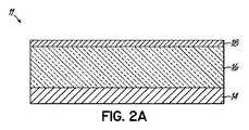
ここで図面−特に図1−を参照すると、半導体11(図2A)を製造するため、誘電層上でのアスペクト比トラッピング(“ART”)を用いた材料のヘテロエピタキシャル成長の一方法を表すフローチャート10が示されている。図2A-図2Gは、図1に供される方法を概略的に表している。 Referring now to the drawings—particularly FIG. 1—a
工程12では、図2Aを参照すると、上に誘電層16を有する基板14が供される。その結果ハードマスク18が誘電層16上に堆積される。基板14はたとえば、誘電層16を構成する二酸化シリコン(SiO2)を有する従来のシリコン系材料であって良い。ハードマスク18は単層であって良いし又は多層であっても良い。少なくとも1層はシリコンを含み、少なくとも1層はシリコンと酸素を含み、又は、少なくとも1層は金属を含む。たとえば金属含有ハードマスク層18は、チタン(Ti)、チタン窒化物(TiNy)、タンタル(Ta)、タンタル窒化物(TaNy)、アルミニウム(Al)、又はアルミニウム-銅合金(Al-Cu)、誘電材料−たとえばシリコンカーバイド(SiCy)、シリコン酸化物(SiOy)、シリコン窒化物(SiNy)、又はシリコン酸窒化物(SiOxNy)−、又はアモルファスカーボン(a-C)を含んで良い。少なくとも1つのハードマスク層18は、気相成長方法−たとえば化学気相成長(“CVD”)法又はプラズマCVD(“PECVD”)法−を用いて生成されて良い。In
図示されていないものの、ハードマスク層18は、たとえば光の波長によってパターニングされ、かつ処理されうるフォトレジスト層をさらに有して良い。フォトレジストパターンは、エッチングプロセス−たとえば乾式プラズマエッチングプロセス又は乾式非プラズマエッチングプロセス−を介してハードマスク層18へ転写されて良い。乾式プラズマエッチングプロセスを利用するとき、プラズマエッチング気体組成物はハロゲン含有化学物質を含んで良い。たとえばプラズマエッチング気体組成物は、Cl2、BCl3、Br2、HBr、SF6、若しくはNF3、又は上記2つ以上の混合物を含んで良い。それに加えてたとえばプラズマエッチング気体組成物は、フルオロカーボン系化学物質−たとえばC4F8、C5F8、C3F6、C4F6、CF4等のうちの少なくとも1つ−又はフルオロハイドロカーボン系化学物質−たとえばCHF3、CH2F2等のうちの少なくとも1つ−を含んで良い。さらに追加の気体は不活性気体−たとえば希ガス−、酸素、水素、窒素、CO2、CO、又は上記2種類以上の混合物を含んで良い。あるいはその代わりに、乾式プラズマエッチングの専門家には明らかなように、フォトレジスト層に対して少なくとも1層のハードマスク層18を選択的にエッチングする任意のエッチングプロセス用化学物質が用いられて良い。Although not shown, the
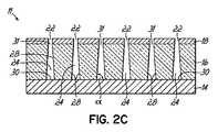
如何なる場合でも、工程20において、誘電層16内部に1つ以上のトレンチ24(図2C)を生成するためにハードマスク層18内に開口部22を供するように、ハードマスク層18が、図2Bに図示されているように、パターニングされ、エッチングされ、かつ、穴を空けられる。 In any case, in
図2Cに図示されているように、工程26では、1つ以上のトレンチ24が、シリコン系基板14に対する誘電層16のレトログレードエッチングによって生成されて良い。レトログレードエッチング−深掘り反応性イオンエッチング(“DRIE”)系プロセスである−の結果、トレンチ24は、シリコン基板14の表面30に対して角度αをなす側壁28を有する。ここでαは約45°〜約90°の範囲であって良い。換言すると、トレンチ24は、シリコン基板14の表面30から、ハードマスク層18で生成される開口部31へ向かって先細って良い。さらに別な表現を用いて説明すると、各トレンチ24の底部(ここではトレンチ24内部で曝露される基板14の表面30)が、開口部31の横方向寸法(たとえば長さ、幅、又は直径)よりも大きい横方向寸法を有する。一例によると、横方向寸法(開口部対底部)の比は2〜3の範囲であって良い。 As shown in FIG. 2C, in step 26, one or
トレンチ24を生成する代表的なDRIEプロセスは、シリコンに対する非常に速いエッチング速度、高アスペクト比、及び酸化物に対する高い選択性を特徴とするボッシュエッチングプロセスを含んで良い。ボッシュエッチングプロセスは、エッチングと保護のサイクルを交互に繰り返す異方性エッチングを含む。エッチング工程中、原料気体−たとえばSF6−から生成されるプラズマは、誘電層16の材料をエッチングするのに用いられる。保護工程中、原料気体−たとえばC4F8−から生成されるプラズマは、化学的に不活性な層によってトレンチ24の側壁28をコーティングする。保護層は、後続のエッチング工程中に側壁28の横方向へ進行するエッチングを制御することができる。An exemplary DRIE process for producing
あるいはその代わりに、トレンチ24を生成する他のDRIEプロセスは、側壁28をエッチングするSF6プラズマと側壁28を保護するハライド系化学物質(HBr/Cl2/O2,HBr/O2又はCl2/O2,)を同時に用いる。Alternatively, other DRIE processes that produce
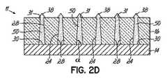
一旦トレンチの生成が完了すると、ハードマスク層18は工程32において除去され、かつ、工程34において、トレンチ24は、ARTを用いた材料のヘテロエピタキシャル成長によって充填される。材料は、高電子移動度を有する化合物を含み、かつ、記載されている本発明の実施例によると、ゲルマニウム、III-V族化合物、又はそれら2つ以上の混合物を含んで良い。III-V族化合物は、周期表のIII族とV族からの元素を含む(たとえばガリウムヒ素(GaAs)、インジウム燐(InP)、インジウム燐ヒ素(InPAs)、及び他当業者に知られているもの等)。 Once trench formation is complete, the
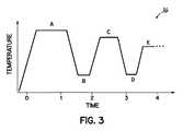
一の典型的なARTプロセスによると、図2Cと図3のタイムライン36に図示されているように、基板14は、トレンチ24の側壁28上の酸化膜を除去する還元環境中で予熱されて良い(工程A)。基板14の温度は低下し(工程B)、それにより第1緩衝層(たとえばGaAs)がトレンチ24内部に堆積されうる。誘電層16とその続いて成長した結晶50との間での格子不整合を解決することの可能な緩衝層が図2Dに図示されている。基板温度は、堆積された緩衝層からの結晶成長のために昇温されて良い。再度基板14の温度は低下する(工程D)。その結果第2緩衝層(たとえば同じGaAsでも良いし又は異なるInPであっても良い)がトレンチ24内部に堆積される。温度は昇温して、さらなる結晶成長を助ける。低温での緩衝層堆積と高温での結晶成長との二段階処理は、図2Dに図示されているように第1過成長38が各トレンチ24上方に生成されるまで、何回でも繰り返される。 According to one exemplary ART process, the
ここで図1、図2D、及び図2Eを参照すると、化学機械研磨(“CMP”)方法が、第1過成長38を除去するように実行されて良い(工程40)。本発明の一の実施例によると、KOH、コロイド状シリカ、及びNaOCl、NH4OH、又はH2O2のうちの1つ以上を含む研磨スラリーが、表面の汚染を導入することなく、第1過成長38を構成する余剰材料を除去するために研磨パッドと併用される。他のCMP方法が用いられて良く、かつ、本発明は本明細書で供された特定の例に限定されないことに留意して欲しい。Referring now to FIGS. 1, 2D, and 2E, a chemical mechanical polishing (“CMP”) method may be performed to remove the first overgrowth 38 (step 40). According to one embodiment of the present invention, a polishing slurry comprising KOH, colloidal silica, and one or more of NaOCl, NH4 OH, or H2 O2 may be used without introducing surface contamination. 1 Used in combination with a polishing pad to remove excess material constituting overgrowth 38. Note that other CMP methods may be used and the invention is not limited to the specific examples provided herein.
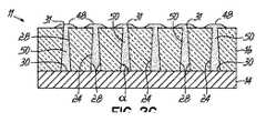
ここで図1、図2F、及び図2Gを参照する。工程42によると、ARTを用いたヘテロエピタキシャル成長が、各トレンチ24の上方に第2過成長44を生成するように繰り返されて良い。第2過成長44も、工程46において第2CMPプロセスによって除去されることで、たとえばCMOSデバイスのさらなる製造に用いられるのに適した平坦なプラトー48が生成される。 Reference is now made to FIGS. 1, 2F, and 2G. According to step 42, heteroepitaxial growth using ART may be repeated to produce second overgrowth 44 above each
本発明の一の実施例による図1のプロセスは、従来方法と比較して、CMOSデバイスの製造中に生成される転位を数を減少させる。その点では、プロセスは、ある面積内での許される転位の数(転位密度)を抑制するように最適化されて良い。その点では、たとえ具体的に例示されていないとしても、所定の転位密度が選択される。前記所定の転位密度は、たとえば所望の電子移動度又は許容レベルの汚染に部分的に基づいて良い。一の典型的な方法では、所定の転位密度は、1cm3あたりe10の転位〜1cm3あたりe22の転位の範囲であって良い。The process of FIG. 1 according to one embodiment of the present invention reduces the number of dislocations generated during the fabrication of CMOS devices compared to conventional methods. In that regard, the process may be optimized to reduce the number of dislocations allowed (dislocation density) within an area. In that respect, a predetermined dislocation density is selected even if not specifically exemplified. The predetermined dislocation density may be based in part on, for example, a desired electron mobility or acceptable level of contamination. In one exemplary method, the predetermined dislocation density may range from dislocation of the
使用時及び工程46後に、図2Gの半導体11が除去され、かつ、各トレンチ24内部の材料の転位密度が、たとえば透過型電子顕微鏡、電界イオンで顕微鏡等によって測定されて良い。測定された転位密度が所定の転位密度の選択された範囲内である場合、半導体11はさらに処理されて良い。あるいはその代わりに、転位密度が所定の転位密度を超える場合、上述のプロセスの工程うちの1つ以上が変更されて良い。そのような工程は、ART中にトレンチ24のアスペクト比又はレトログレード角を変更する工程、材料50を変更する工程、又は1層以上の緩衝層を追加する工程を含む。変更されたプロセスは新たな半導体で実行されて良い。その後その新たな半導体は同様の方法で評価される。 During use and after
ここで図4を参照すると、CMOS集積のためのFIN置き換え方法に関するフローチャート60が、本発明の一の実施例に従って記載されている。その点では、さらに図5Aを参照すると、工程68において、所望の寸法のFIN構造64を有する基板62が供され、かつ、誘電層66が基板62上に堆積される。工程70では、図5Bに図示されているように、誘電層66が、FIN構造64上に開口上部69を生成するように、化学機械平坦化−たとえば図2Eで説明したプロセスのような処理−によって処理される。 Referring now to FIG. 4, a
工程72では、マスク74が、置き換え用に選ばれなかったそれらのFIN構造−以降非選択FIN構造64bと呼ぶ−に適用されうる一方で、選択されたFIN構造64aは、図5Cに図示されているようにマスクされないままである。従って選択されたFIN構造64aは、非選択FIN構造64bを処理することなくさらに処理されて良い。具体的には、選択されたFIN構造64a内のシリコンは、たとえば選択されたFIN構造64aからシリコンを選択的にエッチングするエッチングプロセス(工程76)によって、図4において、図5Dに図示されているように除去される。続いて工程82では、ARTを用いた第1材料78のヘテロエピタキシャル成長が、図1の工程34を参照しながら説明した方法で処理されて良い。材料は、ゲルマニウム、III-V族化合物、又はそれら2つ以上の混合物のうちの少なくとも1つを含んで良い。過成長80が、図5Eに図示されているように選択されたFIN構造64aの各々の上方に生成されるまで、工程82におけるARTプロセスは続く。過成長80は続いて、図5Fに図示されているように、化学機械平坦化によって工程82において除去される。工程82の化学機械平坦化はまた、非選択FIN構造64bからマスク74をも除去して良い。 In step 72,
図示されていないとはいえ、図1の工程42と46で詳細に説明したように、第2過成長が選択されたFIN構造64a上に生成され、その後除去されて良いことに留意して欲しい。 Note that although not shown, a second overgrowth may be generated on the selected
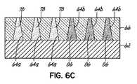
必要であれば、図5Fの基板62は、さらなるCMOS製造において用いられて良いし、又は、以降で詳述するように、本明細書で述べたさらなるプロセスを受け手も良い。より具体的には、図4と図6Aを参照すると、非選択FIN構造のシリコンは、工程84において除去され、かつ、続いて工程88においてARTプロセスを用いたヘテロエピタキシャル成長によって、図6Bに図示されているように、第2材料86に置き換えられる。必要ないとはいえ、第2材料86は高電子移動度の第1材料78とは一般的には異なるだけではなく、ゲルマニウム、III-V族化合物、又はそれら2つ以上の混合物のうちの少なくとも1つをも含む。図6Bに図示されているように、過成長90が非選択FIN構造64bの各々の上方に生成されるまで結晶成長は続く。過成長90はその後、図6Cに図示されているように化学機械平坦化によって除去される。 If necessary, the
ここでも必要な場合には、第2過成長が、非選択FIN構造64b上に生成され、かつ、その後非選択FIN構造64bから除去されて良い。それに加えてFIN構造のマスク処理は、複数のFIN構造を、複数のFIN構造からなる2つの群又は2つの部分に限定する必要はない。その代わりに、第1マスクは、FIN構造の第1部分集合の材料を置き換えるのに用いられて良い。第1マスクの除去後、FIN構造の第2部分集合の材料を置き換えるように、第2マスクが用いられて良い。よってプロセスにおいて用いられるマスクの数は、特定のCMOSデバイスにおいて必要とされるFIN構造の部分集合の数に関連する。さらに本明細書では示されていないが、基板の反対面が、上述のように、又は、集積回路の製造と調和する他の工程に従って処理されて良い。 Again, if necessary, the second overgrowth may be generated on the
必要であれば、置き換えられたFIN構造は、転位の数を測定し、かつ、その転位の数と所定の数とを比較することによって、上述の方法に従って評価されて良い。 If necessary, the replaced FIN structure may be evaluated according to the method described above by measuring the number of dislocations and comparing the number of dislocations with a predetermined number.
本明細書で詳述しているように、半導体デバイスの製造方法は、誘電層内部でのトレンチのレトログレードエッチング、ARTを用いた材料のヘテロエピタキシャル成長、及び、結果として得られた過成長の平坦化を含む。トレンチのレトログレードエッチングは、トレンチ内部での材料の転位密度をさらに減少させ、かつ、後続の処理のために前記トレンチの構造耐久性を増大させる。 As detailed herein, semiconductor device fabrication methods include retrograde etching of trenches within dielectric layers, heteroepitaxial growth of materials using ART, and resulting overgrowth planarization. Including Retrograde etching of the trench further reduces the dislocation density of the material inside the trench and increases the structural durability of the trench for subsequent processing.
Claims (20)
Translated fromJapanese(a) 上に誘電層を有し、かつ、前記誘電層上にマスク層を有する基板を供する工程;
(b) 前記マスク層をパターニング及び現像する工程;
(c) レトログレードエッチングによって前記誘電層内に複数のトレンチを生成する工程;
(d) アスペクト比トラッピングによるヘテロエピタキシャル成長によって、ゲルマニウム、III-V族化合物、又は上記2つ以上の混合物のうちの少なくとも1つを含む材料を前記複数のトレンチに過充填する工程;並びに、
(e) 前記の過充填された複数のトレンチを平坦化する工程;
を有する方法。A method for manufacturing a semiconductor device comprising:
(a) providing a substrate having a dielectric layer thereon and having a mask layer on the dielectric layer;
(b) patterning and developing the mask layer;
(c) generating a plurality of trenches in the dielectric layer by retrograde etching;
(d) overfilling the plurality of trenches with a material comprising at least one of germanium, a III-V compound, or a mixture of the two or more by heteroepitaxial growth by aspect ratio trapping; and
(e) planarizing the plurality of overfilled trenches;
Having a method.
前記少なくとも1つの側壁は、前記底部に対してレトログレード角をなし、かつ、
前記レトログレード角は45°乃至90°の範囲である、
請求項1に記載の方法。Each of the plurality of trenches has at least one sidewall, a bottom, and an opening facing the bottom,
The at least one sidewall forms a retrograde angle with respect to the bottom; and
The retrograde angle is in the range of 45 ° to 90 °,
The method of claim 1.
前記底部の横方向寸法に対する前記開口部の横方向寸法の比は2乃至5の範囲である、
請求項1に記載の方法。Each of the plurality of trenches has at least one sidewall, a bottom, and an opening facing the bottom,
The ratio of the lateral dimension of the opening to the lateral dimension of the bottom is in the range of 2 to 5.
The method of claim 1.
(g) 前記の測定された転位密度と所定の転位密度とを比較する工程;及び、
(h) 前記の測定された転位密度が所定の転位密度未満であるときに前記基板をさらに処理するか、又は、前記ART中に前記複数のトレンチのアスペクト比を変更する工程、前記複数のトレンチのレトログレード角を変更する工程、前記材料を変更する工程、若しくは1層以上の緩衝層を追加する工程を実行する一方で、前記基板を新たな基板に置き換え、かつ、前記(a)乃至(e)を前記新たな基板で反復する工程;
をさらに有する、請求項1に記載の方法。(f) measuring the dislocation density inside each of the plurality of trenches;
(g) comparing the measured dislocation density with a predetermined dislocation density; and
(h) further processing the substrate when the measured dislocation density is less than a predetermined dislocation density, or changing the aspect ratio of the plurality of trenches during the ART, the plurality of trenches The step of changing the retrograde angle, the step of changing the material, or the step of adding one or more buffer layers, while replacing the substrate with a new substrate, and (a) to (a) repeating e) with the new substrate;
The method of claim 1, further comprising:
前記複数のトレンチは、前記少なくとも1つのn型電界効果型トランジスタのFIN構造を構成する、
請求項1に記載の方法。The semiconductor device has at least one p-type field effect transistor and at least one n-type field effect transistor;
The plurality of trenches constitute a FIN structure of the at least one n-type field effect transistor;
The method of claim 1.
(g) 前記の過充填された複数のトレンチを平坦化することで、前記複数のトレンチの各々で平坦化されたプラトーを生成する工程;
をさらに有する、請求項1に記載の方法。(f) overfilling the plurality of trenches with the material again by heteroepitaxial growth by aspect ratio trapping; and
(g) planarizing the plurality of overfilled trenches to produce a planarized plateau in each of the plurality of trenches;
The method of claim 1, further comprising:
(a) 複数のFIN構造と該複数のFIN構造の各々を取り囲む誘電層を有する基板を供する工程であって、
前記複数のFIN構造の各々は、底部、開口部、及び前記底部と前記開口部との間で延びる少なくとも1つの側壁を有し、
前記底部の横方向寸法は、前記開口部の横方向寸法よりも大きい、
工程;
(b) 前記複数のFIN構造の第1部分をマスクする一方で、前記複数のFIN構造の第2部分をマスクしないままにする工程;
(c) 前記複数のFIN構造の第2部分をエッチングする工程;
(d) アスペクト比トラッピングによるヘテロエピタキシャル成長によって、ゲルマニウム、III-V族化合物、又は上記2つ以上の混合物のうちの少なくとも1つを含む第1材料によって前記複数のFIN構造の第2部分を過充填する工程;並びに、
(e) 前記の過充填された複数のFIN構造の第2部分を平坦化する工程;
を有する、方法。A method for manufacturing a semiconductor device comprising:
(a) providing a substrate having a plurality of FIN structures and a dielectric layer surrounding each of the plurality of FIN structures,
Each of the plurality of FIN structures has a bottom, an opening, and at least one sidewall extending between the bottom and the opening;
The lateral dimension of the bottom is greater than the lateral dimension of the opening;
Process;
(b) masking a first portion of the plurality of FIN structures while leaving a second portion of the plurality of FIN structures unmasked;
(c) etching a second portion of the plurality of FIN structures;
(d) Overfilling the second portion of the plurality of FIN structures with a first material comprising at least one of germanium, a III-V compound, or a mixture of two or more of the above by heteroepitaxial growth by aspect ratio trapping And a step of
(e) planarizing the second portion of the overfilled plurality of FIN structures;
Having a method.
(g) アスペクト比トラッピングによるヘテロエピタキシャル成長によって、ゲルマニウム、III-V族化合物、又は上記2つ以上の混合物のうちの前記少なくとも1つとは異なる1つを含む第2材料によって前記複数のFIN構造の第1部分を過充填する工程;並びに、
(h) 前記の過充填された複数のFIN構造の第1部分を平坦化する工程;
を有する、請求項12に記載の方法。(f) etching a first portion of the plurality of FIN structures;
(g) by heteroepitaxial growth by aspect ratio trapping, the second material of the plurality of FIN structures is formed by a second material comprising germanium, a group III-V compound, or a different one from the at least one of the two or more mixtures. Overfilling one part; and
(h) planarizing the first portion of the overfilled FIN structures;
13. The method of claim 12, comprising:
前記複数のFIN構造の第2部分が少なくとも1つのn型電界効果型トランジスタに組み込まれる、
請求項13に記載の方法。A first portion of the plurality of FIN structures is incorporated into at least one p-type field effect transistor; and
A second portion of the plurality of FIN structures is incorporated into at least one n-type field effect transistor;
The method according to claim 13.
前記レトログレード角は45°乃至90°の範囲である、
請求項12に記載の方法。At least one sidewall of each of the plurality of FIN structures forms a retrograde angle with respect to each corresponding one bottom of the plurality of FIN structures; and
The retrograde angle is in the range of 45 ° to 90 °,
The method according to claim 12.
前記複数のFIN構造の各々の底部の横方向寸法に対する前記複数のFIN構造の各対応する一の開口部の横方向寸法の比は2乃至5の範囲である、請求項12に記載の方法。Each of the plurality of trenches has at least one sidewall, a bottom, and an opening facing the bottom,
13. The method of claim 12, wherein the ratio of the lateral dimension of each corresponding one opening of the plurality of FIN structures to the lateral dimension of the bottom of each of the plurality of FIN structures is in the range of 2-5.
(g) 前記の測定された転位密度と所定の転位密度とを比較する工程;及び、
(h) 前記の測定された転位密度が所定の転位密度未満であるときに前記基板をさらに処理するか、又は、前記ART中に前記複数のFIN構造のアスペクト比を変更する工程、前記複数のFIN構造のレトログレード角を変更する工程、前記第1材料を変更する工程、若しくは1層以上の緩衝層を追加する工程を実行する一方で、前記基板を新たな基板に置き換え、かつ、前記(a)乃至(e)を前記新たな基板で反復する工程;
をさらに有する、請求項12に記載の方法。(f) measuring a dislocation density in a first portion of each of the plurality of FIN structures;
(g) comparing the measured dislocation density with a predetermined dislocation density; and
(h) further processing the substrate when the measured dislocation density is less than a predetermined dislocation density, or changing the aspect ratio of the plurality of FIN structures during the ART; While changing the retrograde angle of the FIN structure, changing the first material, or adding one or more buffer layers, replacing the substrate with a new substrate, and ( repeating steps a) to (e) with the new substrate;
13. The method of claim 12, further comprising:
Applications Claiming Priority (3)
| Application Number | Priority Date | Filing Date | Title |
|---|---|---|---|
| US201161556215P | 2011-11-05 | 2011-11-05 | |
| US61/556,215 | 2011-11-05 | ||
| PCT/US2012/063108WO2013067212A1 (en) | 2011-11-05 | 2012-11-01 | Epitaxial film growth in retrograde wells for semiconductor devices |
Publications (1)
| Publication Number | Publication Date |
|---|---|
| JP2015502657Atrue JP2015502657A (en) | 2015-01-22 |
Family
ID=52437206
Family Applications (1)
| Application Number | Title | Priority Date | Filing Date |
|---|---|---|---|
| JP2014540096APendingJP2015502657A (en) | 2011-11-05 | 2012-11-01 | Epitaxial film growth in retrograde wells for semiconductor devices. |
Country Status (1)
| Country | Link |
|---|---|
| JP (1) | JP2015502657A (en) |
Citations (6)
| Publication number | Priority date | Publication date | Assignee | Title |
|---|---|---|---|---|
| US6134207A (en)* | 1996-07-30 | 2000-10-17 | Seagate Technology, Inc. | Optical data storage system having optical microswitch |
| US6355567B1 (en)* | 1999-06-30 | 2002-03-12 | International Business Machines Corporation | Retrograde openings in thin films |
| US6518071B1 (en)* | 2002-03-28 | 2003-02-11 | Motorola, Inc. | Magnetoresistive random access memory device and method of fabrication thereof |
| WO2006125040A2 (en)* | 2005-05-17 | 2006-11-23 | Amberwave Systems Corporation | Lattice-mismatched semiconductor structures with reduced dislocation defect densities related methods for device fabrication |
| US20100025683A1 (en)* | 2008-07-01 | 2010-02-04 | Amberwave Systems Corporation | Reduction of edge effects from aspect ration trapping |
| JP2011063502A (en)* | 2009-09-18 | 2011-03-31 | Taiwan Semiconductor Manufacturing Co Ltd | Semiconductor device and method for production of semiconductor structure |
- 2012
- 2012-11-01JPJP2014540096Apatent/JP2015502657A/enactivePending
Patent Citations (6)
| Publication number | Priority date | Publication date | Assignee | Title |
|---|---|---|---|---|
| US6134207A (en)* | 1996-07-30 | 2000-10-17 | Seagate Technology, Inc. | Optical data storage system having optical microswitch |
| US6355567B1 (en)* | 1999-06-30 | 2002-03-12 | International Business Machines Corporation | Retrograde openings in thin films |
| US6518071B1 (en)* | 2002-03-28 | 2003-02-11 | Motorola, Inc. | Magnetoresistive random access memory device and method of fabrication thereof |
| WO2006125040A2 (en)* | 2005-05-17 | 2006-11-23 | Amberwave Systems Corporation | Lattice-mismatched semiconductor structures with reduced dislocation defect densities related methods for device fabrication |
| US20100025683A1 (en)* | 2008-07-01 | 2010-02-04 | Amberwave Systems Corporation | Reduction of edge effects from aspect ration trapping |
| JP2011063502A (en)* | 2009-09-18 | 2011-03-31 | Taiwan Semiconductor Manufacturing Co Ltd | Semiconductor device and method for production of semiconductor structure |
Similar Documents
| Publication | Publication Date | Title |
|---|---|---|
| US8481341B2 (en) | Epitaxial film growth in retrograde wells for semiconductor devices | |
| CN110660735B (en) | Stress Modulation for Dielectric Layers | |
| US9373546B2 (en) | Self aligned replacement Fin formation | |
| US12027625B2 (en) | Semiconductor device having fins and method of fabricating the same | |
| US8946026B2 (en) | Methods of fabricating a semiconductor device including metal gate electrodes | |
| TWI713120B (en) | Methods for fabricating semiconductor device and fin field effect transistor | |
| TW201926548A (en) | Semiconductor structure manufacturing method | |
| US20200144050A1 (en) | Lattice-Mismatched Semiconductor Substrates with Defect Reduction | |
| CN108987275A (en) | Method for manufacturing semiconductor device | |
| US10163623B1 (en) | Etch method with surface modification treatment for forming semiconductor structure | |
| TWI801628B (en) | Methods to protect nitride layers during formation of silicon germanium nano-wires in microelectronic workpieces | |
| CN108735604A (en) | The forming method of transistor | |
| US10276449B1 (en) | Method for forming fin field effect transistor (FinFET) device structure | |
| CN108807377B (en) | Semiconductor device and method of forming the same | |
| US20240363425A1 (en) | Multi-channel devices and methods of manufacture | |
| JP2008218999A (en) | Method of manufacturing semiconductor device | |
| TWI851705B (en) | Method of anisotropically etching adjacent lines with multi-color selectivity | |
| JP2015502657A (en) | Epitaxial film growth in retrograde wells for semiconductor devices. | |
| TW201724360A (en) | Method for producing semiconductor device | |
| CN102832163B (en) | method of opening | |
| US20140175513A1 (en) | Structure And Method For Integrated Devices On Different Substartes With Interfacial Engineering |
Legal Events
| Date | Code | Title | Description |
|---|---|---|---|
| A131 | Notification of reasons for refusal | Free format text:JAPANESE INTERMEDIATE CODE: A131 Effective date:20150929 | |
| A521 | Request for written amendment filed | Free format text:JAPANESE INTERMEDIATE CODE: A523 Effective date:20151127 | |
| A131 | Notification of reasons for refusal | Free format text:JAPANESE INTERMEDIATE CODE: A131 Effective date:20160517 | |
| A02 | Decision of refusal | Free format text:JAPANESE INTERMEDIATE CODE: A02 Effective date:20161115 |