JP2015500562A - Micro light emitting diode - Google Patents
Micro light emitting diodeDownload PDFInfo
- Publication number
- JP2015500562A JP2015500562AJP2014542349AJP2014542349AJP2015500562AJP 2015500562 AJP2015500562 AJP 2015500562AJP 2014542349 AJP2014542349 AJP 2014542349AJP 2014542349 AJP2014542349 AJP 2014542349AJP 2015500562 AJP2015500562 AJP 2015500562A
- Authority
- JP
- Japan
- Prior art keywords
- micro
- diode
- layer
- micro led
- top surface
- Prior art date
- Legal status (The legal status is an assumption and is not a legal conclusion. Google has not performed a legal analysis and makes no representation as to the accuracy of the status listed.)
- Pending
Links
Images


Classifications
- H—ELECTRICITY
- H10—SEMICONDUCTOR DEVICES; ELECTRIC SOLID-STATE DEVICES NOT OTHERWISE PROVIDED FOR
- H10H—INORGANIC LIGHT-EMITTING SEMICONDUCTOR DEVICES HAVING POTENTIAL BARRIERS
- H10H20/00—Individual inorganic light-emitting semiconductor devices having potential barriers, e.g. light-emitting diodes [LED]
- H10H20/80—Constructional details
- H10H20/81—Bodies
- H10H20/811—Bodies having quantum effect structures or superlattices, e.g. tunnel junctions
- H10H20/812—Bodies having quantum effect structures or superlattices, e.g. tunnel junctions within the light-emitting regions, e.g. having quantum confinement structures
- F—MECHANICAL ENGINEERING; LIGHTING; HEATING; WEAPONS; BLASTING
- F21—LIGHTING
- F21V—FUNCTIONAL FEATURES OR DETAILS OF LIGHTING DEVICES OR SYSTEMS THEREOF; STRUCTURAL COMBINATIONS OF LIGHTING DEVICES WITH OTHER ARTICLES, NOT OTHERWISE PROVIDED FOR
- F21V7/00—Reflectors for light sources
- H—ELECTRICITY
- H01—ELECTRIC ELEMENTS
- H01L—SEMICONDUCTOR DEVICES NOT COVERED BY CLASS H10
- H01L21/00—Processes or apparatus adapted for the manufacture or treatment of semiconductor or solid state devices or of parts thereof
- H01L21/67—Apparatus specially adapted for handling semiconductor or electric solid state devices during manufacture or treatment thereof; Apparatus specially adapted for handling wafers during manufacture or treatment of semiconductor or electric solid state devices or components ; Apparatus not specifically provided for elsewhere
- H01L21/677—Apparatus specially adapted for handling semiconductor or electric solid state devices during manufacture or treatment thereof; Apparatus specially adapted for handling wafers during manufacture or treatment of semiconductor or electric solid state devices or components ; Apparatus not specifically provided for elsewhere for conveying, e.g. between different workstations
- H—ELECTRICITY
- H10—SEMICONDUCTOR DEVICES; ELECTRIC SOLID-STATE DEVICES NOT OTHERWISE PROVIDED FOR
- H10D—INORGANIC ELECTRIC SEMICONDUCTOR DEVICES
- H10D62/00—Semiconductor bodies, or regions thereof, of devices having potential barriers
- H10D62/10—Shapes, relative sizes or dispositions of the regions of the semiconductor bodies; Shapes of the semiconductor bodies
- H10D62/124—Shapes, relative sizes or dispositions of the regions of semiconductor bodies or of junctions between the regions
- H—ELECTRICITY
- H10—SEMICONDUCTOR DEVICES; ELECTRIC SOLID-STATE DEVICES NOT OTHERWISE PROVIDED FOR
- H10H—INORGANIC LIGHT-EMITTING SEMICONDUCTOR DEVICES HAVING POTENTIAL BARRIERS
- H10H20/00—Individual inorganic light-emitting semiconductor devices having potential barriers, e.g. light-emitting diodes [LED]
- H10H20/01—Manufacture or treatment
- H10H20/011—Manufacture or treatment of bodies, e.g. forming semiconductor layers
- H10H20/018—Bonding of wafers
- H—ELECTRICITY
- H10—SEMICONDUCTOR DEVICES; ELECTRIC SOLID-STATE DEVICES NOT OTHERWISE PROVIDED FOR
- H10H—INORGANIC LIGHT-EMITTING SEMICONDUCTOR DEVICES HAVING POTENTIAL BARRIERS
- H10H20/00—Individual inorganic light-emitting semiconductor devices having potential barriers, e.g. light-emitting diodes [LED]
- H10H20/80—Constructional details
- H10H20/81—Bodies
- H10H20/811—Bodies having quantum effect structures or superlattices, e.g. tunnel junctions
- H—ELECTRICITY
- H10—SEMICONDUCTOR DEVICES; ELECTRIC SOLID-STATE DEVICES NOT OTHERWISE PROVIDED FOR
- H10H—INORGANIC LIGHT-EMITTING SEMICONDUCTOR DEVICES HAVING POTENTIAL BARRIERS
- H10H20/00—Individual inorganic light-emitting semiconductor devices having potential barriers, e.g. light-emitting diodes [LED]
- H10H20/80—Constructional details
- H10H20/81—Bodies
- H10H20/822—Materials of the light-emitting regions
- H10H20/823—Materials of the light-emitting regions comprising only Group II-VI materials, e.g. ZnO
- H—ELECTRICITY
- H10—SEMICONDUCTOR DEVICES; ELECTRIC SOLID-STATE DEVICES NOT OTHERWISE PROVIDED FOR
- H10H—INORGANIC LIGHT-EMITTING SEMICONDUCTOR DEVICES HAVING POTENTIAL BARRIERS
- H10H20/00—Individual inorganic light-emitting semiconductor devices having potential barriers, e.g. light-emitting diodes [LED]
- H10H20/80—Constructional details
- H10H20/81—Bodies
- H10H20/822—Materials of the light-emitting regions
- H10H20/824—Materials of the light-emitting regions comprising only Group III-V materials, e.g. GaP
- H—ELECTRICITY
- H10—SEMICONDUCTOR DEVICES; ELECTRIC SOLID-STATE DEVICES NOT OTHERWISE PROVIDED FOR
- H10H—INORGANIC LIGHT-EMITTING SEMICONDUCTOR DEVICES HAVING POTENTIAL BARRIERS
- H10H29/00—Integrated devices, or assemblies of multiple devices, comprising at least one light-emitting semiconductor element covered by group H10H20/00
- H10H29/10—Integrated devices comprising at least one light-emitting semiconductor component covered by group H10H20/00
- H—ELECTRICITY
- H01—ELECTRIC ELEMENTS
- H01L—SEMICONDUCTOR DEVICES NOT COVERED BY CLASS H10
- H01L2224/00—Indexing scheme for arrangements for connecting or disconnecting semiconductor or solid-state bodies and methods related thereto as covered by H01L24/00
- H01L2224/93—Batch processes
- H01L2224/95—Batch processes at chip-level, i.e. with connecting carried out on a plurality of singulated devices, i.e. on diced chips
- H—ELECTRICITY
- H01—ELECTRIC ELEMENTS
- H01L—SEMICONDUCTOR DEVICES NOT COVERED BY CLASS H10
- H01L25/00—Assemblies consisting of a plurality of semiconductor or other solid state devices
- H01L25/03—Assemblies consisting of a plurality of semiconductor or other solid state devices all the devices being of a type provided for in a single subclass of subclasses H10B, H10D, H10F, H10H, H10K or H10N, e.g. assemblies of rectifier diodes
- H01L25/04—Assemblies consisting of a plurality of semiconductor or other solid state devices all the devices being of a type provided for in a single subclass of subclasses H10B, H10D, H10F, H10H, H10K or H10N, e.g. assemblies of rectifier diodes the devices not having separate containers
- H01L25/075—Assemblies consisting of a plurality of semiconductor or other solid state devices all the devices being of a type provided for in a single subclass of subclasses H10B, H10D, H10F, H10H, H10K or H10N, e.g. assemblies of rectifier diodes the devices not having separate containers the devices being of a type provided for in group H10H20/00
- H01L25/0753—Assemblies consisting of a plurality of semiconductor or other solid state devices all the devices being of a type provided for in a single subclass of subclasses H10B, H10D, H10F, H10H, H10K or H10N, e.g. assemblies of rectifier diodes the devices not having separate containers the devices being of a type provided for in group H10H20/00 the devices being arranged next to each other
- H—ELECTRICITY
- H10—SEMICONDUCTOR DEVICES; ELECTRIC SOLID-STATE DEVICES NOT OTHERWISE PROVIDED FOR
- H10H—INORGANIC LIGHT-EMITTING SEMICONDUCTOR DEVICES HAVING POTENTIAL BARRIERS
- H10H20/00—Individual inorganic light-emitting semiconductor devices having potential barriers, e.g. light-emitting diodes [LED]
- H10H20/80—Constructional details
- H10H20/81—Bodies
- H10H20/819—Bodies characterised by their shape, e.g. curved or truncated substrates
Landscapes
- Engineering & Computer Science (AREA)
- General Engineering & Computer Science (AREA)
- Physics & Mathematics (AREA)
- Condensed Matter Physics & Semiconductors (AREA)
- General Physics & Mathematics (AREA)
- Manufacturing & Machinery (AREA)
- Computer Hardware Design (AREA)
- Microelectronics & Electronic Packaging (AREA)
- Power Engineering (AREA)
- Led Devices (AREA)
- Photo Coupler, Interrupter, Optical-To-Optical Conversion Devices (AREA)
- Electroluminescent Light Sources (AREA)
- Led Device Packages (AREA)
- Light Receiving Elements (AREA)
Abstract
Translated fromJapaneseDescription
Translated fromJapanese本発明は、マイクロ半導体デバイスに関する。より具体的には、本発明の実施形態は、異なる基板に転写させるための発光ダイオード(LED)などのマイクロデバイスのアレイを形成する方法に関する。 The present invention relates to a micro semiconductor device. More specifically, embodiments of the present invention relate to a method of forming an array of microdevices such as light emitting diodes (LEDs) for transfer to different substrates.
(関連出願の相互参照)
本出願は、2011年11月18日に出願された米国仮特許出願第61/561,706号、及び2012年2月3日に出願された米国仮特許出願第61/594,919号に基づく優先権を主張し、これらの出願の全開示を参照により本願明細書に引用する。(Cross-reference of related applications)
This application is based on US Provisional Patent Application No. 61 / 561,706, filed November 18, 2011, and US Provisional Patent Application No. 61 / 594,919, filed February 3, 2012. Priority is claimed and the entire disclosures of these applications are incorporated herein by reference.
窒化ガリウム(GaN)を原料とする発光ダイオード(LED)は、白熱灯及び蛍光灯に代わって将来の効率の高い照明用途で使用されると期待されている。現行のGaN系LEDデバイスは、異種基板材料上のヘテロエピタキシャル成長法により作製される。一般的なウェーハレベルのLEDデバイス構造は、サファイア成長用基板の上に形成される下部のn型にドープされた(n型)GaN層、単一量子井戸(SQW)又は多重量子井戸(MWQ)、並びに、上部のp型にドープされた(p型)GaN層を含み得る。 Light emitting diodes (LEDs) made from gallium nitride (GaN) are expected to be used in future efficient lighting applications in place of incandescent and fluorescent lamps. Current GaN-based LED devices are fabricated by heteroepitaxial growth on different substrate materials. Typical wafer level LED device structures include a lower n-type doped (n-type) GaN layer, single quantum well (SQW) or multiple quantum well (MWQ) formed on a sapphire growth substrate. As well as an upper p-type doped (p-type) GaN layer.
一実装形態では、ウェーハレベルのLEDデバイス構造は、上部のp型GaN層と量子井戸層を通じて、n型GaN層にエッチング処理することで、サファイア成長用基板上でメサ・アレイ(array of mesas)へとパターン形成される。上部のp電極は、メサ・アレイの最上部のp型GaN表面上に形成され、n電極は、メサ・アレイと接触するn型GaN層の一部分の上に形成される。メサ形LEDデバイスは、最終製品内のサファイア成長用基板上に残留する。 In one implementation, a wafer level LED device structure is etched into an n-type GaN layer through an upper p-type GaN layer and a quantum well layer, thereby forming an array of mesas on a sapphire growth substrate. The pattern is formed. The upper p-electrode is formed on the top p-type GaN surface of the mesa array, and the n-electrode is formed on a portion of the n-type GaN layer that contacts the mesa array. The mesa LED device remains on the sapphire growth substrate in the final product.
別の実装形態では、ウェーハレベルのLEDデバイス構造を、成長用基板からシリコンなどのアクセプタ基板へと転写させる。これには、GaN/サファイア複合構造よりも簡単にダイシングして個々のチップを形成し易いという利点がある。この実施形態では、ウェーハレベルのLEDデバイス構造は、恒久的な接合層によりアクセプタ(シリコン)基板に恒久的に接合されている。例えば、メサ・アレイのp型GaN表面上に形成されたp型電極は、恒久的な接合層によりアクセプタ(シリコン)基板に接合することができる。次いで、サファイア成長用基板を除去して、反転したウェーハレベルのLEDデバイス構造を露出し、これを薄化加工して、メサ・アレイを露出させる。次に、露出したn型GaNでn接触部を作製し、更に、p電極と電気的に接触するシリコン基板上にp接触部を作製する。メサ形LEDデバイスは、最終製品のアクセプタ基板上に残る。更に、GaN/シリコン複合基板をダイシングして、個々のチップを形成できる。 In another implementation, the wafer level LED device structure is transferred from a growth substrate to an acceptor substrate such as silicon. This has the advantage that it is easier to form individual chips by dicing than a GaN / sapphire composite structure. In this embodiment, the wafer level LED device structure is permanently bonded to the acceptor (silicon) substrate by a permanent bonding layer. For example, a p-type electrode formed on a p-type GaN surface of a mesa array can be bonded to an acceptor (silicon) substrate by a permanent bonding layer. The sapphire growth substrate is then removed to expose the inverted wafer level LED device structure, which is thinned to expose the mesa array. Next, an n-contact portion is formed from the exposed n-type GaN, and a p-contact portion is formed on a silicon substrate that is in electrical contact with the p-electrode. The mesa LED device remains on the acceptor substrate of the final product. Furthermore, individual chips can be formed by dicing the GaN / silicon composite substrate.
マイクロ発光ダイオード(LED)及び転写先基板(receiving substrate)に転写する(transfer)ためのマイクロLEDアレイを形成する方法について述べている。例えば、転写先基板は、限定されないが、ディスプレイ基板、照明基板、トランジスタ、若しくは集積回路(IC)などの機能デバイスを有する基板、又は金属再配線付き基板が可能である。一実施形態では、マイクロLED構造体は、マイクロp−nダイオード及び金属層を含み、この金属層は、マイクロp−nダイオードと基板上に形成された接合層との間に配置される。金属層は、1つ以上の層を含むことが可能である。例えば、金属層は、電極層、及び電極層と接合層との間にあるバリア層を含み得る。マイクロp−nダイオード及び金属層はそれぞれ、最上面、底面、及び側壁を有し得る。一実施形態では、マイクロp−nダイオードの底面は、マイクロp−nダイオードの最上面よりも広く、側壁は、上部から底部まで外側に向かって先細形状になっている。更に、マイクロp−nダイオードの最上面は、このp−nダイオードの底面よりも広い又はほぼ同じであってもよい。一実施形態では、マイクロp−nダイオードの底面は、金属層の最上面よりも広い。マイクロp−nダイオードの底面は、金属層の最上面よりも広い、又は金属層の最上面とほぼ同じ幅でもよい。 A method of forming a micro LED array for transfer to a micro light emitting diode (LED) and a receiving substrate is described. For example, the transfer destination substrate is not limited, and can be a display substrate, a lighting substrate, a transistor, a substrate having a functional device such as an integrated circuit (IC), or a substrate with metal rewiring. In one embodiment, the micro LED structure includes a micro pn diode and a metal layer, the metal layer being disposed between the micro pn diode and a junction layer formed on the substrate. The metal layer can include one or more layers. For example, the metal layer can include an electrode layer and a barrier layer between the electrode layer and the bonding layer. The micro pn diode and the metal layer can each have a top surface, a bottom surface, and a sidewall. In one embodiment, the bottom surface of the micro pn diode is wider than the top surface of the micro pn diode, and the sidewalls taper outward from the top to the bottom. Furthermore, the top surface of the micro pn diode may be wider or substantially the same as the bottom surface of the pn diode. In one embodiment, the bottom surface of the micro pn diode is wider than the top surface of the metal layer. The bottom surface of the micro pn diode may be wider than the top surface of the metal layer or may be approximately the same width as the top surface of the metal layer.
任意選択で、共形誘電バリア層はマイクロp−nダイオード及び他の露出面の上方に形成可能である。共形誘電バリア層がその上に形成しようとする形状の輪郭を形成するように、共形誘電バリア層は、マイクロp−nダイオード、金属層、及び任意選択で接合層よりも薄くすることが可能である。一実施形態では、共形誘電バリア層は、マイクロp−nダイオードの側壁に広がり、マイクロp−nダイオード内の量子井戸層を覆うことができる。共形誘電バリア層は、マイクロp−nダイオードの底面に広がってもよく、並びに金属層の側壁に広がってもよい。いくつかの実施形態では、共形誘電バリア層はまた、パターン形成された接合層の側壁に広がる。共形誘電バリア層に、マイクロp−nダイオードの最上面を露出する接触開口部を形成できる。接触開口部は、マイクロp−nダイオードの最上面よりも広い幅、狭い幅、又はほぼ同じ幅を有してもよい。一実施形態では、接触開口部は、マイクロp−nダイオードの最上面の幅よりも狭い幅を有し、共形誘電バリア層は、マイクロp−nダイオードの最上面の縁部周囲にリップ部を形成できる。 Optionally, a conformal dielectric barrier layer can be formed over the micro pn diode and other exposed surfaces. The conformal dielectric barrier layer may be thinner than the micro pn diode, the metal layer, and optionally the junction layer so that the conformal dielectric barrier layer forms a profile of the shape to be formed thereon. Is possible. In one embodiment, the conformal dielectric barrier layer can extend to the sidewalls of the micro pn diode and cover the quantum well layer in the micro pn diode. The conformal dielectric barrier layer may extend on the bottom surface of the micro pn diode as well as on the sidewalls of the metal layer. In some embodiments, the conformal dielectric barrier layer also extends to the sidewalls of the patterned bonding layer. A contact opening can be formed in the conformal dielectric barrier layer exposing the top surface of the micro pn diode. The contact opening may have a width that is wider, narrower, or substantially the same as the top surface of the micro pn diode. In one embodiment, the contact opening has a width that is narrower than the width of the top surface of the micro pn diode, and the conformal dielectric barrier layer has a lip around the edge of the top surface of the micro pn diode. Can be formed.
いくつかの実施形態では、接合層は、約350℃より低い、より具体的には、約200℃より低い液相線温度又は融点を有する材料で形成できる。例えば、接合層は、インジウム、スズ又はポリエチレン若しくはポリプロピレンなどの熱可塑性高分子を含められる。接合層は、基板全体にわたり横方向に連続的である、又は横方向に分離した箇所で形成されてもよい。例えば、接合層の横方向に分離した箇所は、幅がマイクロp−nダイオード又は金属層の底面よりも狭い幅若しくはほぼ同じ幅を有してもよい。 In some embodiments, the bonding layer can be formed of a material having a liquidus temperature or melting point below about 350 ° C., more specifically below about 200 ° C. For example, the bonding layer can include indium, tin or a thermoplastic polymer such as polyethylene or polypropylene. The bonding layer may be laterally continuous across the entire substrate or may be formed at locations separated laterally. For example, the laterally separated portions of the bonding layer may have a width that is narrower than or substantially the same as the bottom surface of the micro pn diode or metal layer.
一実施形態では、マイクロLEDアレイは、キャリア基板上の接合層の複数の箇、並びに接合層の複数の箇所上の対応する複数のマイクロLED構造体を含む。各マイクロLED構造体は、マイクロp−nダイオード及び金属層を含み、この金属層は、マイクロp−nダイオードと接合層の対応する箇所との間に配置される。共形誘電バリア層は、基板上のマイクロLEDアレイ上に成膜可能であり、この共形誘電バリア層は、各マイクロp−nダイオードの側壁に広がる。更に、共形誘電バリア層は、各マイクロp−nダイオードの底面、及び各金属層の側壁にも部分的に広がってもよい。各マイクロp−nダイオードの最上面を露出する複数の接触開口部を、共形誘電バリア層に形成可能であり、各接触開口部は、対応する各マイクロp−nダイオードの最上面よりも広いか、狭いか又はほぼ同じであり得る幅を有する。 In one embodiment, the micro LED array includes a plurality of bonding layers on the carrier substrate, as well as a corresponding plurality of micro LED structures on multiple locations of the bonding layer. Each micro LED structure includes a micro pn diode and a metal layer, which metal layer is disposed between the micro pn diode and a corresponding portion of the junction layer. A conformal dielectric barrier layer can be deposited on the micro LED array on the substrate, and the conformal dielectric barrier layer extends to the sidewalls of each micro pn diode. Furthermore, the conformal dielectric barrier layer may also partially extend to the bottom surface of each micro pn diode and to the sidewalls of each metal layer. A plurality of contact openings exposing the top surface of each micro pn diode can be formed in the conformal dielectric barrier layer, each contact opening being wider than the top surface of each corresponding micro pn diode. Or a width that can be narrow or approximately the same.
接合層の複数の箇所は、互いに横方向に分離する又は横方向に分離しなくてもよい。一実施形態では、接合層の複数の箇所は、横方向に分離されており、共形誘電バリア層は、接合層の複数の横方向に分離した箇所それぞれの側壁に広がる。一実施形態では、基板は、その上に接合層の複数の箇所が形成される、対応する複数のピラーを含む。例えば、各マイクロp−nダイオードはいずれか、対応するピラーの最上面とほぼ同じ幅であるか、又は対応するピラーの最上面よりも広い底面を含むことが可能である。更に、ピラーは、高さが接合層の箇所の対応する厚さよりも高くてもよい。一実施形態では、対応する高さは、対応する厚さの少なくとも2倍である。 The plurality of portions of the bonding layer may or may not be separated from each other in the lateral direction. In one embodiment, the plurality of locations of the bonding layer are laterally separated, and the conformal dielectric barrier layer extends to the sidewalls of each of the plurality of laterally separated locations of the bonding layer. In one embodiment, the substrate includes a corresponding plurality of pillars on which a plurality of locations of the bonding layer are formed. For example, each micro pn diode can either include a bottom surface that is approximately the same width as the top surface of the corresponding pillar, or wider than the top surface of the corresponding pillar. Furthermore, the pillar may be higher in height than the corresponding thickness at the location of the bonding layer. In one embodiment, the corresponding height is at least twice the corresponding thickness.
マイクロLED構造体及びマイクロLEDアレイは、既存の異種機能材料成長法(heterogeneous growth)を使用してパターン形成可能である。一実施形態では、p−nダイオード層及び金属層は、成長用基板からキャリア基板へと転写される。本発明の実施形態によれば、p−nダイオード層及び金属層は、キャリア基板への転写前又は転写後にパターン形成可能である。p−nダイオード層及び金属層をキャリア基板に転写する工程は、金属層をキャリア基板上の接合層に接合する工程を含んでもよい。例えば、接合層は、約350℃より低い、より具体的には、約200℃より低い液相線温度又は融点を有し得る。例えば、接合層をインジウム又はインジウム合金から形成できる。p−nダイオード層及び金属層をパターン形成して、複数の分離されたマイクロp−nダイオード及び金属層の複数の分離した箇所を形成した後、共形誘電バリア層が、複数の分離されたマイクロp−nダイオードの側壁に広がって形成される。共形誘電バリア層は、これが形成される形状の外形を形成可能であり、並びにマイクロp−nダイオード及び金属層よりも薄くてもよい。例えば、共形誘電バリア層は、原子層堆積(ALD)法により形成可能である。更に、共形誘電バリア層は、分離された各マイクロp−nダイオードの底面の一部分の上にも形成可能である。 Micro LED structures and micro LED arrays can be patterned using existing heterogeneous growth methods. In one embodiment, the pn diode layer and the metal layer are transferred from the growth substrate to the carrier substrate. According to embodiments of the present invention, the pn diode layer and the metal layer can be patterned before or after transfer to the carrier substrate. The step of transferring the pn diode layer and the metal layer to the carrier substrate may include a step of bonding the metal layer to a bonding layer on the carrier substrate. For example, the bonding layer may have a liquidus temperature or melting point below about 350 ° C., more specifically below about 200 ° C. For example, the bonding layer can be formed from indium or an indium alloy. After patterning the pn diode layer and the metal layer to form a plurality of isolated portions of the micro pn diode and the metal layer, the conformal dielectric barrier layer is separated into a plurality. It is formed so as to spread on the side wall of the micro pn diode. The conformal dielectric barrier layer can form the outer shape of the shape in which it is formed, and may be thinner than the micro pn diode and the metal layer. For example, the conformal dielectric barrier layer can be formed by atomic layer deposition (ALD). Furthermore, a conformal dielectric barrier layer can also be formed on a portion of the bottom surface of each isolated micro pn diode.
一実施形態では、p−nダイオード層及びp−nダイオード層上の金属層の複数の分離した箇所を含むパターン形成された金属層は、成長用基板からキャリア基板へと転写される。トレンチによって分離されたマイクロ・メサをp−nダイオード層内で形成するために、p−nダイオード層は、成長用基板からキャリア基板へ転写される前に部分的にパターン形成されてもよい。一実施形態では、p−nダイオード層及びパターン形成された金属層をキャリア基板に転写する前に、複数のピラーがキャリア基板上に形成される。p−nダイオード層及びパターン形成された金属層をキャリア基板に転写する前に、接合層をキャリア基板上の複数のピラーの上方に形成可能である。 In one embodiment, a patterned metal layer that includes a pn diode layer and a plurality of discrete locations of the metal layer on the pn diode layer is transferred from a growth substrate to a carrier substrate. In order to form micro mesas separated by trenches in the pn diode layer, the pn diode layer may be partially patterned before being transferred from the growth substrate to the carrier substrate. In one embodiment, a plurality of pillars are formed on the carrier substrate prior to transferring the pn diode layer and the patterned metal layer to the carrier substrate. Prior to transferring the pn diode layer and the patterned metal layer to the carrier substrate, a bonding layer can be formed over the plurality of pillars on the carrier substrate.
一実施形態では、金属層及びp−nダイオード層を成長用基板からキャリア基板に転写した後、金属層をパターン形成して、金属層の複数の分離した箇所を形成する。このような実施形態では、p−nダイオード層をパターン形成して、複数の分離されたマイクロp−nダイオードを形成し、その後、金属層をパターン形成する。金属層のパターン形成工程には、金属層の複数の分離した箇所の最大幅が複数の分離されたマイクロp−nダイオードそれぞれの底面の幅よりも狭くなるまで、金属層をエッチング処理する工程を含めてもよい。一実施形態では、p−nダイオード層及び金属層を成長用基板からキャリア基板に転写した後で、接合層をパターン形成する。例えば、接合層の複数の分離した箇所の最大幅が複数の分離したマイクロp−nダイオードそれぞれの底面の幅よりも狭くなるまで、接合層をエッチング処理可能である。p−nダイオード層及び金属層を成長用基板からキャリア基板に移送する前に、複数のピラーもキャリア基板上に形成されてもよい。p−nダイオード層及びパターン形成された金属層をキャリア基板に移送する前に、接合層はキャリア基板上の複数のピラーの上方に形成されてもよい。 In one embodiment, after the metal layer and the pn diode layer are transferred from the growth substrate to the carrier substrate, the metal layer is patterned to form a plurality of separated portions of the metal layer. In such an embodiment, the pn diode layer is patterned to form a plurality of isolated micro pn diodes, and then the metal layer is patterned. The metal layer pattern forming step includes a step of etching the metal layer until the maximum width of the plurality of separated portions of the metal layer becomes narrower than the width of the bottom surface of each of the plurality of separated micro pn diodes. May be included. In one embodiment, the bonding layer is patterned after the pn diode layer and the metal layer are transferred from the growth substrate to the carrier substrate. For example, the bonding layer can be etched until the maximum width of the plurality of separated portions of the bonding layer becomes narrower than the width of the bottom surface of each of the plurality of separated micro pn diodes. A plurality of pillars may also be formed on the carrier substrate before transferring the pn diode layer and the metal layer from the growth substrate to the carrier substrate. Prior to transferring the pn diode layer and the patterned metal layer to the carrier substrate, a bonding layer may be formed over the plurality of pillars on the carrier substrate.
形成後、マイクロLED構造体及びマイクロLEDアレイはピックアップされ、転写先基板に転写されてもよい。転写ヘッドは、マイクロLED構造体のアレイを配置したキャリア基板の上方に配置可能であり、少なくとも1つのマイクロLED構造体の接合層内で相転移をもたらすための操作が実行される。この操作は、例えば、液相線温度若しくは融点より高温での接合層の加熱、又は接合層の結晶相の変化であってもよい。マイクロp−nダイオード、金属層、及び任意選択で、少なくとも1つのマイクロLED構造体における接合層の一部分を含む少なくとも1つのLED構造体を、移送ヘッドでピックアップして、これを転写先基板上に配置できる。共形誘電バリア層がすでに形成されている場合、共形誘電バリア層の一部も、マイクロp−nダイオード及び金属層と共にピックアップできる。あるいは、共形誘電バリア層は、これを転写先基板上に配置した後で、マイクロLED構造体又は複数のマイクロLED構造体の上方に形成可能である。 After formation, the micro LED structure and the micro LED array may be picked up and transferred to a transfer destination substrate. The transfer head can be placed above the carrier substrate on which the array of micro LED structures is placed, and an operation is performed to cause a phase transition in the bonding layer of the at least one micro LED structure. This operation may be, for example, heating the bonding layer at a liquidus temperature or higher than the melting point, or changing the crystal phase of the bonding layer. At least one LED structure comprising a micro pn diode, a metal layer, and optionally a portion of the bonding layer in at least one micro LED structure is picked up by a transfer head and placed on the destination substrate. Can be placed. If a conformal dielectric barrier layer has already been formed, a portion of the conformal dielectric barrier layer can also be picked up with the micro pn diode and the metal layer. Alternatively, the conformal dielectric barrier layer can be formed over the micro LED structure or the plurality of micro LED structures after it is disposed on the destination substrate.
一実施形態では、共形誘電バリア層は、マイクロp−nダイオードの底面の一部分に広がり、金属層の側壁に広がり、並びに、金属層と隣接する接合層の一部の全体に広がる。共形誘電バリア層は、マイクロLED構造体と移送ヘッドとの接触、及び/又は、接合層内の位相変化の生成後に切断でき、切断は移送ヘッドによるマイクロp−nダイオード及び金属層のピックアップよりも前であってもよい。例えば、共形誘電バリア層の切断工程には、移送ヘッドから共形誘電バリア層までの圧力の伝達工程、及び/又は、接合層の液相線温度を超えて接合層を加熱する工程を含めてもよい。 In one embodiment, the conformal dielectric barrier layer extends over a portion of the bottom surface of the micro pn diode, extends over the sidewalls of the metal layer, and extends over the entire portion of the junction layer adjacent to the metal layer. The conformal dielectric barrier layer can be cut after contact between the micro LED structure and the transfer head and / or the generation of a phase change in the bonding layer, the cutting being from picking up the micro pn diode and metal layer by the transfer head. May be before. For example, the step of cutting the conformal dielectric barrier layer includes the step of transmitting pressure from the transfer head to the conformal dielectric barrier layer and / or heating the bonding layer above the liquidus temperature of the bonding layer. May be.
本発明の実施形態では、マイクロ半導体デバイス及び転写先基板に転写するためのマイクロ発光ダイオード(LED)などのマイクロ半導体デバイス・アレイを形成する方法について述べている。例えば、転写先基板は、限定されないが、ディスプレイ基板、照明基板、トランジスタ若しくは集積回路(IC)などの機能デバイスを有する基板、又は金属再配線付き基板が可能である。本発明の実施形態は、p−nダイオードを含むマイクロLEDに関して具体的に説明しているが、本発明の実施形態はこれに限定されず、更に、特定の実施形態は、所定の電子機能(例えば、ダイオード、トランジスタ、集積回路)、又はフォトニック機能(LED、レーザ)を制御された様式で実行するように設計された他のマイクロ半導体デバイスにも適用可能であることを理解するべきである。 Embodiments of the present invention describe a method of forming a micro semiconductor device array, such as a micro semiconductor device and a micro light emitting diode (LED) for transfer to a transfer destination substrate. For example, the transfer destination substrate is not limited, but can be a display substrate, a lighting substrate, a substrate having a functional device such as a transistor or an integrated circuit (IC), or a substrate with metal rewiring. While embodiments of the present invention have been described specifically with respect to micro-LEDs that include pn diodes, embodiments of the present invention are not limited thereto, and specific embodiments may also have a predetermined electronic function ( For example, it should be understood that it is also applicable to other microsemiconductor devices designed to perform a controlled function in a controlled manner (eg, diodes, transistors, integrated circuits) or photonic functions (LEDs, lasers). .
種々の実施形態では、図面を参照して説明する。だが、特定の実施形態は、これらの具体的な詳細の1つ以上を使用することなく、又は他の公知の方法及び構成を併用することで、実施可能である。以下の説明では、本発明に関する深い理解を提供するために、具体的な構成、寸法、及びプロセスなどの多数の具体的な詳細について説明する。他の例では、本発明を不必要に曖昧とさせないために、公知の半導体プロセスや製造技術について、具体的に説明していない。本明細書を通じた「一実施形態(one embodiment)」、「一実施形態(an embodiment)」等への言及は、本実施形態と関連して述べる特定の機能、構造、構成、又は特徴は、本発明に関する少なくとも一実施形態の中に含まれることを意味する。したがって、本明細書全体の種々の場所における語句「一実施形態(one embodiment)」、「一実施形態(an embodiment)」等の出現は必ずしも、本発明の同じ実施形態について言及するものではない。更に、特定の機能、構造、構成、又は特徴は、1つ以上の実施形態の中で何らかの適切な方法により組合せることが可能である。 Various embodiments will be described with reference to the drawings. However, certain embodiments may be practiced without using one or more of these specific details or in combination with other known methods and configurations. In the following description, numerous specific details are set forth, such as specific configurations, dimensions, and processes, in order to provide a thorough understanding of the present invention. In other instances, well-known semiconductor processes and fabrication techniques have not been described in detail so as not to unnecessarily obscure the present invention. References to “one embodiment”, “an embodiment”, and the like throughout this specification refer to specific functions, structures, configurations, or features described in connection with this embodiment, It is meant to be included in at least one embodiment relating to the present invention. Thus, the appearances of the phrases “one embodiment”, “an embodiment”, and the like in various places throughout this specification are not necessarily referring to the same embodiment of the invention. Furthermore, the particular functions, structures, configurations, or features may be combined in any suitable manner within one or more embodiments.
本明細書で使用される用語「広がる(spanning)」、「〜の上方に(over)」、「〜への(to)」、「〜間の(between)、及び「〜上に(on)」は、他の層に対するある層の相対位置について言及する場合がある。ある層が別の層に「広がる」、「の上方に」若しくは「上に」あること、又は別の層「へと」接合することは、別の層と直接接触する、又は1つ以上の介在層を有することが想定される。層「間の」ある層は、層に直接接触する、又は1つ以上の介在層を含むことがある。 The terms “spanning”, “over”, “to”, “between” and “on” as used herein. "May refer to the relative position of one layer relative to another. One layer “spreading”, “above” or “on” another layer, or joining “to” another layer is in direct contact with one or more than one It is envisaged to have an intervening layer. Some layers “between” the layers may be in direct contact with the layer or may include one or more intervening layers.
本明細書で使用される用語「マイクロ」デバイス、「マイクロ」p−nダイオード、又は「マイクロ」LED構造体は、本発明の実施形態に係るあるデバイス、又は構造体の記述的なサイズを言及する場合がある。本明細書において、用語「マイクロ」デバイス、又は構造体は、1から100μmまでのスケールを言及することを意味する。だが、本発明の実施形態はこれに限定されず、実施形態の特定の態様は、これより大きいか、これよりも小さなサイズ・スケールにも適用可能であることを理解するべきである。 As used herein, the term “micro” device, “micro” pn diode, or “micro” LED structure refers to a descriptive size of a device or structure according to embodiments of the present invention. There is a case. As used herein, the term “micro” device, or structure, is meant to refer to a scale from 1 to 100 μm. However, it is to be understood that embodiments of the present invention are not so limited and that certain aspects of the embodiments are applicable to larger or smaller size scales.
一態様では、本発明の実施形態は、バルク型LED基板を、ピックアップして転写先基板に転写するように準備されたマイクロLED構造体アレイに処理する方法について述べている。これにより、マイクロLED構造体を異種機能集積システム(heterogeneously integrated system)に統合し、組み立てることが可能である。マイクロLED構造体は、個別に、纏めて、又は完全なアレイとしてピックアップされ、転写されてもよい。したがって、マイクロLED構造体アレイ内のマイクロLED構造体は、ピックアップされて、マイクロディスプレイから大型ディスプレイまで任意のサイズのディスプレイ基板などの転写先基板へ高速転写速度で転写するよう準備される。いくつかの実施形態では、ピックアップのために準備されるマイクロLED構造体アレイは、10μm×10μmピッチ、又は5μm×5μmピッチであるものとして説明している。これらの密度において、例えば、15.2cm(6インチ)基板は、10μm×10μmピッチで約1億6千5百万個のマイクロLED構造体、及び5μm×5μmピッチでは約6億6千万個のマイクロLED構造体を収容できる。したがって、所定機能を有する高密度な製造済みマイクロデバイスが、ピックアップし転写先基板に転写するように準備される様式で製造可能である。本明細書で述べた方法は、マイクロLED構造体に限定されず、他のマイクロデバイスの製造においても使用可能である。 In one aspect, embodiments of the present invention describe a method of processing a bulk LED substrate into a micro LED structure array that is prepared to be picked up and transferred to a destination substrate. This allows the micro LED structure to be integrated and assembled into a heterogeneously integrated system. The micro LED structures may be picked up and transferred individually, collectively or as a complete array. Accordingly, the micro LED structures in the micro LED structure array are picked up and prepared for transfer at a high transfer rate from a micro display to a large display to a transfer destination substrate such as a display substrate of any size. In some embodiments, the micro LED structure array prepared for pickup is described as having a 10 μm × 10 μm pitch, or 5 μm × 5 μm pitch. At these densities, for example, a 15.2 cm (6 inch) substrate has about 165 million micro LED structures at a 10 μm × 10 μm pitch, and about 660 million at a 5 μm × 5 μm pitch. The micro LED structure can be accommodated. Accordingly, a high density manufactured microdevice having a predetermined function can be manufactured in a manner prepared to be picked up and transferred to a transfer destination substrate. The methods described herein are not limited to micro LED structures, but can be used in the manufacture of other microdevices.
別の態様では、本発明の実施形態は、各マイクロp−nダイオードが接合層の対応する箇所の上方に形成されるマイクロLED構造体、及びマイクロLEDアレイについて説明している。接合層の対応する箇所は、横方向に分離された箇所であってもよく、又は横方向に分離された箇所でなくてもよい。マイクロLEDのピックアップ工程中は、マイクロLEDに対応する接合層の対応する箇所の上で操作が実行可能であるが、そのピックアップ工程中に接合層の対応する箇所はピックアップ工程の助けとなる相転移を起こす。例えば、接合層の対応する箇所は、温度サイクルに反応して固体から液体に変化する場合がある。液体状態では、接合層の対応する箇所は、表面張力によりマイクロp−nダイオードをキャリア基板上で定位置に保持しながら、同時に、マイクロp−nダイオードが容易にリリース可能な媒体も提供する。更に、液体状態は、ピックアップ工程中に転写ヘッドがマイクロLED構造体と接触する場合、転写ヘッドがもたらす力を吸収するためのクッション又は衝撃吸収材としても機能することができる。このようにして、液体状態は、転写ヘッドがもたらす圧縮力に反応して、下にある面全体を平滑化することで、マイクロLEDアレイ、又は転写ヘッドアレイにおける形状の不均一性を補正できる。他の実施形態では、接合層の対応する箇所が相転移を完全には起こさないことがある。例えば、接合層の対応する箇所は、部分的に固体状態であるものの、温度サイクルに反応して実質的に十分な柔軟性を有する場合がある。別の実施形態では、接合層の対応する箇所は、温度サイクルのなどの操作に反応して、結晶相転移を起こすこともある。 In another aspect, embodiments of the present invention describe micro LED structures and micro LED arrays in which each micro pn diode is formed above a corresponding location in the junction layer. The corresponding part of the bonding layer may be a part separated in the lateral direction or may not be a part separated in the lateral direction. During the pick-up process of the micro LED, the operation can be performed on the corresponding part of the bonding layer corresponding to the micro LED, but the corresponding part of the bonding layer during the pick-up process is a phase transition that helps the pick-up process. Wake up. For example, the corresponding location of the bonding layer may change from a solid to a liquid in response to a temperature cycle. In the liquid state, the corresponding portion of the bonding layer also provides a medium in which the micro pn diode can be easily released while holding the micro pn diode in place on the carrier substrate by surface tension. Furthermore, the liquid state can also function as a cushion or shock absorber to absorb the force provided by the transfer head when the transfer head contacts the micro LED structure during the pick-up process. In this way, the liquid state can compensate for the shape non-uniformity in the micro LED array or transfer head array by smoothing the entire underlying surface in response to the compressive force provided by the transfer head. In other embodiments, corresponding portions of the bonding layer may not completely cause the phase transition. For example, the corresponding portion of the bonding layer may be substantially solid in response to a temperature cycle, although partially in the solid state. In another embodiment, the corresponding portion of the bonding layer may undergo a crystalline phase transition in response to an operation such as a temperature cycle.
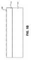
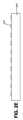
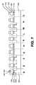
ここで図1を参照すると、半導体デバイス層110は基板101上に形成可能である。一実施形態では、半導体デバイス層110は、1つ以上の層を含むことが可能であり、所定の電子機能(例えば、ダイオード、トランジスタ、集積回路)、又はフォトニック機能(LED、レーザ)を制御された様式で実行するよう設計されている。半導体デバイス層110は、所定機能の中で制御された様式で実行するよう設計可能であるが、半導体デバイス層110は、完全に機能的でない可能性があることを理解するべきである。例えば、アノード又はカソードなどの接触部は、まだ形成されていない場合がある。簡潔さのため及び本発明の実施形態を曖昧とさせないために、以下では、従来の異種機能材料成長条件に従って成長用基板101上で成長させたp−nダイオード層110としての半導体デバイス層110について説明している。 Referring now to FIG. 1, the
p−nダイオード層110は、スペクトルの所定領域に対応するバンドギャップを有する化合物半導体を含むことができる。例えば、p−nダイオード層110は、II〜VI族材料(例えば、ZnSe)、又はIII〜V族窒化物材料(例えば、GaN、AlN、InN、及びその合金)を原料とする1つ以上の層を含むことができる。成長用基板101は、限定されないが、シリコン、SiC、GaAs、GaN、及びサファイア(Al2O3)などの任意の適切な基板を含むことができる。The
特定の実施形態では、成長用基板101は、サファイアであり、p−nダイオード層110は、GaNから形成される。サファイアはGaNに対して大きな格子定数と熱膨張係数不整合を有するにも関わらず、サファイアはコストが合理的に低く、広範囲で利用可能であり、その透明性は、エキシマレーザに基づくリフトオフ(LLO)法と相性がいい。別の実施形態では、SiCなどの別な材料もGaN p−nダイオード層110用の成長用基板101として使用可能である。サファイアのように、SiC基板は透過性でよい。有機金属化学気相成長法(MOCVD)などの、幾つかの成長法は、p−nダイオード層110の成長において使用可能である。例えば、GaNは、トリメチルガリウム(TMGa)及びアンモニア(NH3前駆物質をサファイア成長用基板101と共に反応チャンバへと同時に導入し、800℃から1,000℃などの高温まで加熱することで成長可能である。図1Aで説明した特定の実施形態では、p−nダイオード層110は、バルクGaN層112、n型層114、量子井戸116、並びにp型層118を含むことが可能である。バルクGaN層112は、シリコン若しくは酸素汚染によりn型にドープされている、又はシリコンのようなドナーにより意図的にドープ可能である。同様に、n型GaN層114は、シリコンなどのドナーでドープ可能であり、p型層118は、マグネシウムなどのアクセプタでドープ可能である。種々の代替的なp−nダイオード構成を用いて、p−nダイオード層110を形成できる。同様に、種々の単一量子井戸(SQW)又は多重量子井戸(MQW)構成を用いて、量子井戸116を形成できる。更に、必要に応じて、種々のバッファ層も含められる。一実施形態では、サファイア成長用基板101は、厚さが約200μmであり、バルクGaN層112は、厚さが約5μmであり、n型層114は、厚さが約0.1μm〜3μmであり、量子井戸層116は、厚さが約0.3μm未満であり、p型層118は、厚さが約0.1μm〜1μmである。In certain embodiments, the
次に、金属層120を、p−nダイオード層110の上方に形成可能である。図1Aで説明するように、金属層120は、電極層122及び他の層も含む場合があるが任意選択でバリア層124を含んでもよい。一実施形態では、金属層は、厚さが約0.1μm〜2μmである。電極層122は、p型GaN層118とオーム接触して、Ni、Au、Ag、Pd、及びPtなどの高仕事関数金属から形成可能である。一実施形態では、電極層122は、光放射に対して反射性である。別の実施形態では、電極層122は、光放射に対して透過性でもよい。透過性は、光吸収を最小とするよう、電極層を極めて薄く作製することで実現可能である。バリア層124は、p−nダイオード110への不純物の拡散を防止するようために、任意選択で金属層120に含めることができる。例えば、バリア層124は、限定されないが、Pd、Pt、Ni、Ta、Ti、及びTiWを含んでもよい。特定の実施形態では、バリア層124は、接合層からのp−nダイオード層110内への成分の拡散を抑止できる。 Next, the
本発明の特定の実施形態によれば、p−nダイオード層110及び金属層120は、成長用基板101上で成長させてから、図2A〜図2Eで説明され、以下でより詳細に説明するキャリア基板201へ転写される。以下の図面と説明でより詳細に説明するように、金属層120及びp−nダイオード層110は、キャリア基板201に転写される前にパターン形成可能である。キャリア基板201及び接合層210はまた、p−nダイオード層110及び金属層120をキャリア基板201に転写する前にパターン形成可能である。したがって、本発明の実施形態は、続いて転写先基板に転写するためのマイクロLEDアレイ形成中に、多様な変形形態として実装可能である。 In accordance with certain embodiments of the present invention, the
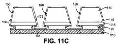
ここで図1Bを参照すると、金属層120は、キャリア基板201に転写する前にパターン形成可能である。一実施形態では、図1Bの構造体は、p−nダイオード層110の上方にパターン形成されたフォトレジスト層を形成してから、金属層120を成膜することで実現可能である。次いで、フォトレジスト層を(フォトレジスト層上の金属層の一部と共に)リフトオフし、図1Bに示すように金属層120の横方向に分離された箇所を残す。一実施形態では、金属層120の横方向に分離された箇所のピッチは、マイクロLEDアレイにピッチに対応して、5μm、10μm、又はこれよりも大きいサイズが可能である。例えば、5μmのピッチは、2μm間隔で分離された金属層120の3μm幅の横方向に分離された箇所から形成され得る。10μmピッチは、2μm間隔を空けた金属層120の8μm幅の横方向に分離された箇所から形成され得る。だが、これらの寸法は例示的であり、本発明の実施形態はこれに限定されない。いくつかの実施形態では、金属層120の横方向に分離された箇所の幅は、以下の説明と図面においてより詳細に論じられるマイクロp−nダイオード150の底面の幅よりも狭い、又はこれに等しい。 Referring now to FIG. 1B, the
ここで図1Cを参照すると、金属層120のパターン形成は、p−nダイオード層110のパターン形成前に実施可能である。一実施形態では、図1Cの構造体は、金属層120の横方向に分離された箇所の上方に2回目のパターン形成されたフォトレジスト層を形成することで実現可能であり、エッチング液を使用して、p−nダイオード層110をエッチング処理することで、トレンチ134をエッチング加工し、複数のマイクロ・メサ130を形成する。図1Aのp−nダイオード層110の拡大部分を再度参照すると、一実施形態では、p型層118、量子井戸116を貫通して、n型層114、又はバルク層112へとトレンチをエッチング加工するエッチング処理を実行する。GaN p−nダイオード層110のエッチング処理は、反応性イオンエッチング(RIE)などのドライプラズマエッチング技術、電子サイクロトロン共鳴(ECR)、誘導結合プラズマ反応性イオンエッチング(ICP−RIE)、及び化学支援イオンビームエッチング(CAIBE)を用いて実施できる。エッチング化学物質は、Cl2、BCl3、又はSiCl4などの化学種を含むハロゲン元素系が可能である。図1Cで説明する特定の実施形態では、マイクロ・メサ130は、15°までの先細形状の側壁132を有することが可能である。例えば、塩素系エッチング化学物質を用いたRIEを利用できる。あるいは、側壁は垂直でもよい。例えば、垂直側壁を得るために、塩素系化学物質を用いるICP−RIEが利用できる。Referring now to FIG. 1C, the patterning of the
特定の実施形態では、マイクロ・メサ130のピッチは、5μm、10μm、又はこれより大きなサイズが可能である。例えば、ピッチが5μmのマイクロ・メサ130アレイは、2μmの間隔を空けた3μm幅のマイクロ・メサから形成できる。ピッチが10μmのマイクロ・メサ130アレイは、2μmの間隔を空けた8μm幅のマイクロ・メサから形成可能である。だが、これらの寸法は例示的であり、本発明の実施形態はこれに限定されない。 In certain embodiments, the pitch of the
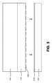
図2A〜図2Eは、金属層120を成長用基板101上に接合するための接合層210を有するキャリア基板201の種々の実施形態について説明する断面側面図である。図2Aは、接合前のパターン形成されていないキャリア基板201及び接合層210を示している。図2B〜図2Dでは、側壁204を有し、トレンチ206で分離された複数のポスト202を形成するようパターン形成されたキャリア基板201を図示している。ポスト202は、マイクロp−nダイオード135、150の幅と等しい、又はこれよりも狭い最大幅を有し、これは、以下の説明と図面において明らかとなるであろう。一実施形態では、トレンチポスト202は、接合層210の厚さの少なくとも2倍の高さである。一実施形態では、接合層210は、厚さが約0.1μm〜2μmでよく、トレンチポストは、高さが少なくとも0.2μm〜4μmである。図2Bで説明する特定の実施形態では、共形の接合層210が、ポスト202の上方に、側壁204上に、そして、トレンチ206の中に形成される。図2Cで説明する特定の実施形態では、接合層210は、側壁204上には多量に成膜されることなく、ポスト202の上面の上及びトレンチ206内にのみ形成されるように異方性成膜される。図2Dで説明する特定の実施形態では、接合層210は、ポスト202の上面の上のみにおいて形成される。このような構成は、同じパターンのフォトレジストでポスト202及び接合層210をパターン形成することで形成可能である。図2Eで説明する特定の実施形態では、接合層210の横方向に分離された箇所は、接合層のブランケット層をパターン形成されたフォトレジスト層の上方に成膜してから、図2Eで説明する接合層210の横方向に分離された箇所を残しつつ、(フォトレジスト層上の接合層の一部と共に)リフトオフするフォトレジスト・リフトオフ法により形成可能である。だが、他の処理技術も利用できる。 2A to 2E are cross-sectional side views illustrating various embodiments of a
図2B〜図2E及び図1B〜図1Cについて先に述べたように、本発明の特定の実施形態は、金属層120の横方向に分離された箇所、及び/又は、接合層210の横方向に分離された箇所を含む。共形の接合層210が、ポスト202の上方、側壁204の上、及びトレンチ206内で形成される図2Bに関して、ポスト202の上の接合層の特定の箇所は、トレンチ206により横方向に分離されている。したがって、共形の接合層210が連続的であっても、ポスト202の上の接合層210の箇所は、横方向に分離された箇所である。同様に、図2Eの接合層210の個々の離散した箇所は、これらの間隔により横方向に隔てられる。ポスト202が存在する場合、接合層210の厚さとポスト202の高さとの関係は、接合層210の横方向の箇所の間隔に考慮される。 As described above with respect to FIGS. 2B-2E and 1B-1C, certain embodiments of the present invention may be provided with laterally separated locations of the
接合層210は、種々の適切な材料から形成可能である。接合層は、マイクロLED構造体をキャリア基板に接着可能な材料から形成できる。一実施形態では、接合層210は、温度変化等の操作に反応して、相転移を受ける場合がある。一実施形態では、相転移を受けて接合層を除去できる。一実施形態では、接合層は再溶融可能又は再流動可能でよい。一実施形態では、接合層は、約350℃より低い、より具体的には、約200℃より低い液相線温度又は融点を有することができる。このような温度において、接合層は、マイクロLED構造体の他の構成要素に著しい影響をもたらさずに、相転移を起こすことがある。例えば、接合層は、金属若しくは金属合金、又は除去可能な熱可塑性高分子から形成できる。一実施形態では、接合層は、伝導性でもよい。例えば、温度の変化に反応して接合層が固体から液体への相転移を起こす場合、接合層の一部は、以下の説明でより詳細に論ずるピックアップ操作中にマイクロLED構造体の上に残ったままである場合がある。このような実施形態では、続いて転写先基板に転写する際、接合層がマイクロLED構造体に悪影響をもたらさないよう、接合層を伝導性の材料から形成する方が有益である場合がある。この場合、転写操作中のマイクロLED構造体に残留する伝導性の接合層の一部分が、マイクロLED構造体を転写先基板上の伝導性パッドへと接合する際に役立つことがある。 The
はんだは、その多くが一般に固体状態の時に延性のある材料であり、半導体及び金属表面との良好なぬれ性を示すことから、接合層210に適した材料とすることができる。一般的な合金は、ある1つの温度ではなく、ある温度範囲において溶融する。したがって、はんだ合金は、合金が液体状態に留まる最低温度に対応する液相線温度及び合金が固体状態に留まる最高温度に対応する固相線温度により、特徴付けられることが多い。本発明の実施形態で使用可能な低融点はんだ材料に関する例示的リストを表1で示す。
本発明の実施形態で使用可能な熱可塑性高分子の例示的リストを表2で示す。
本発明の実施形態によれば、接合層210は、均一の厚さで形成され、特定の組成に応じた種々の適切な方法により成膜可能である。例えば、はんだ組成物は、スパッタリング、電子ビーム(Eビーム)蒸着による成膜、又はシード層を用いためっき処理により、均一な厚さを得ることができる。 According to the embodiment of the present invention, the
ポスト202は、種々の材料及び技術から形成可能である。一実施形態では、ポスト202は、エッチング処理、又はエンボス加工プロセスによりキャリア基板201をパターン形成することで、キャリア基板201と一体的に形成可能である。例えば、キャリア基板201は、ポスト202を一体的に形成したシリコン基板でよい。別の実施形態では、ポストをキャリア基板201の上に形成できる。例えば、ポスト202を、めっき技術及びフォトレジスト・リフトオフ技術により形成可能である。ポストは、半導体、金属、高分子、誘電体等を含む適切な材料から形成できる。 The
ここで図3を参照すると、成長用基板101及びキャリア基板201は、熱及び/又は圧力下で接合可能である。図3は図1Bのパターン形成された構造体と図2Aのパターン形成されていない構造体との接合を示しているが、本発明の実施形態では、図1A〜図1C及び図2A〜図2Eの任意の組合せも考慮されると認識するべきである。更に、接合層210を接合前にキャリア基板201上に形成されると述べてきたが、接合層210は、接合前に成長用基板101の金属層120上に形成することも可能である。例えば、接合層210は、金属層120の上方に形成して、図1Bで説明した金属層の横方向に分離された箇所の形成中に金属層120と一緒にパターン形成できる。説明していないが、接合される両基板上に形成される層の特定の構成や組成に応じ、接合前の酸化を防止するための耐酸化膜を(成長用基板、又はキャリア基板の)いずれかの基板、又は両基板の上面の上に形成できる。例えば、一実施形態では、薄い金の膜を、金属層120及び接合層210の露出面のいずれか、又は両方の上に成膜できる。図3で説明する基板の接合中に、接合層210は、金の膜を部分的に吸収することで、基板間の接合界面において金合金を形成することができる。 Referring now to FIG. 3, the
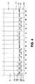
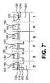
図4は、成長用基板101及びキャリア基板201の接合後における非限定的な、想定される種々の構造体について説明する断面側面図である。表3に基板の特定の組合せを記載する。例えば、実施例4Aで示された特定の実施形態は、図2Dで示されたキャリア基板と図1Cで示された成長用基板との接合を表している。
前述のように、これらの実施例の多くの構造体は、成長用基板上で接合層210を形成してから、成長用基板101をキャリア基板201に接合することでも、作製できる。例えば、実施例4Oは、接合層210と金属層210を成長用基板101上にパターン形成してから、成長用基板101をキャリア基板201に接合することでも、作製できる。 As described above, many structures of these embodiments can be manufactured by forming the
ここで図5を参照すると、成長用基板101は、接合された構造体から除去されている。成長用基板101は、化学的エッチング法、又はこの成長用基板が透明であれば、エキシマレーザに基づくリフトオフ(LLO)などの適切な方法で除去できる。一実施形態では、透明なサファイア成長用基板101からのGaN p−nダイオード層110のLLOは、紫外線レーザ、例えば、Nd−YAGレーザ、又はKrFエキシマレーザからの短パルス(例えば、数十ナノ秒)を透明なサファイア成長用基板101を貫いて101/110層界面を照射することで実現される。界面でのGaN p−nダイオード層110の吸収が、界面の局所化された加熱をもたらし、これにより、界面のGaNにおける液体Ga金属及び窒素ガスへの分解が発生する。所望の領域が照射されたら、透明なサファイア基板101は、ホットプレートの上でGaを再溶融することで除去できる。 Referring now to FIG. 5, the
ここで図6を参照すると、p−nダイオード層110が、望ましい厚さまで薄化加工されている。図1Aの拡大p−nダイオード層110に再度戻ると、薄化加工後に動作可能なp−nダイオードが残留するよう、所定量のバルク状GaN層112(n型でよい)、又はn型GaN層114の一部分を除去する。下部の構造体に応じ、薄化加工プロセスは、研磨、ウェットエッチング処理、又はドライエッチング処理などの適切な方法を用いて実施できる。例えば、研磨、及び/又は、所望の厚さまでの時限エッチングの併用が実行可能である。ピラー、又はマイクロ・メサなどのパターン形成された下部の構造体が存在する状況では、このパターン形成された構造体の損傷を防止するため、所望の厚さまでの時限エッチングが実施可能である。p−nダイオード層110を事前にパターン形成してマイクロ・メサ130を形成する実施例6A、6B、6C、6I、及び6Jで示すように、マイクロ・メサは、この時点で独立したマイクロp−nダイオード135である。 Referring now to FIG. 6, the
成長用基板101、又はキャリア基板201のいずれかが、接合前に事前パターン形成されていない若しくは部分的にのみ事前パターン形成されている場合、図6で説明するp−nダイオード層110の薄化加工後に、追加のパターン形成を実施可能である。図7Aで説明するように、p−nダイオード層110をエッチング処理して独立したマイクロp−nダイオード150を形成するため、パターン形成されていないp−nダイオード層110の上方に、パターン形成されたマスク層140を形成できる。マスク層140は、フォトレジスト、又はフォトレジストよりもGaNエッチング条件に対して耐性の高い金属(例えば、クロム、ニッケル)若しくは誘電体(シリコン窒化物、シリコン酸化物)のような種々の材料から形成できる。GaN p−nダイオード層110のエッチング処理は、反応性イオンエッチング(RIE)、電子サイクロトロン共鳴(ECR)、誘導結合プラズマ反応イオンエッチング(ICP−RIE)、及び化学支援イオンビームエッチング(CAIBE)などのドライプラズマエッチング技術を使って実施可能である。エッチング化学物質は、Cl2、BCl3、又はSiCl4などの化学種を含むハロゲン元素系が可能である。When either the
図7Aで説明した特定の実施形態では、マイクロp−nダイオード層150は、外側に向かって15°まで先細形状の側壁153(マイクロp−nダイオード層150の最上部から底部まで)を有し得る。例えば、塩素系エッチング化学物質を用いたRIEを利用できる。あるいは、側壁153は垂直でもよい。例えば、垂直側壁を得るために、塩素系化学物質を用いるICP−RIEが利用できる。図16の説明で明らかとなるように、ピックアップされた後、転写先基板に転写される一連のマイクロLED構造体の上方に共通接触部を形成する際、いくつかの実施形態では、外側に向かって先細形状の側壁は有利となることがある。一実施形態では、マイクロp−nダイオード150の間のピッチは、5μm、10μm、又はこれよりも大きなサイズが可能である。例えば、ピッチが5μmのマイクロp−nダイオード150アレイは、2μm間隔を空けた3μm幅のマイクロp−nダイオードから形成できる。ピッチが10μmのマイクロp−nダイオード150アレイは、2μm間隔を空けた8μm幅のマイクロp−nダイオードから形成できる。 In the particular embodiment described in FIG. 7A, the micro
ここで図7B〜図7Cを参照すると、エッチング処理は必要に応じて、特定の材料を原料とする金属層120及び接合層210に対して適切なエッチング化学物質を用いて、金属層120及び/又は接合層210に対して継続的に実施可能である。図7Bにおいて図示される一実施形態では、層120、210がマイクロp−nダイオード150の重なり合う下側面と適合する幅を有するよう、ドライエッチング化学物資を用いた異方性エッチングを用いて、金属層120及び/又は接合層210をエッチング処理できる。図7Cで図示される一実施形態では、ウェットエッチング処理を用いて、実施例7CD〜実施例7CHで説明するマイクロp−nダイオード層150の重なり合う下側面より下方の金属層120及び/又は接合層210を「下を削り取り」できる。具体的に説明していないが、マイクロp−nダイオード層135より下方の下部層120、210を「下を削り取り」するために、エッチング処理を更に実行できることも理解されたい。 Referring now to FIGS. 7B-7C, the etching process may be performed using an appropriate etching chemistry for the
マイクロp−nダイオード、金属層、又は接合層のエッチング処理の完了時に、マスク層140を、例えば、選択的エッチング処理等を用いて除去可能であり、これにより、図8で説明するマイクロLEDアレイが得られる。図示のように、マイクロLEDアレイは、キャリア基板201、キャリア基板上の接合層210(横方向に分離されていても、されていなくてもよい)の複数の箇所、並びに、接合層210の複数の箇所の上方にある対応する複数の分離されたマイクロp−nダイオード135、150を含む。金属層120の複数の分離された箇所は、対応する複数の分離されたマイクロp−nダイオード135、150と接合層210の複数の箇所との間に形成される。いくつかの実施形態では、実施例8A〜実施例8F及び実施例8K〜実施例8Mにおいて図示するように、キャリア基板は対応する複数のピラー202を含み、そのピラーの上に、接合層210の横方向に分離された複数の箇所が形成される。 Upon completion of the micro pn diode, metal layer, or bonding layer etching process, the
いくつかの実施形態では、マイクロp−nダイオード150(マイクロp−nダイオード135も同様)は、最上面152及び底面151を含み、金属層120は、最上面121及び底面を含み、マイクロp−nダイオード150(マイクロp−nダイオード135も同様)の底面151は、金属層120の最上面121よりも広い。 In some embodiments, the micro pn diode 150 (as well as the micro pn diode 135) includes a
いくつかの実施形態では、複数のマイクロp−nダイオード135、150それぞれは、対応する複数のピラー202それぞれの最上面203とほぼ同じ幅を有する底面151を含む。他の実施形態では、複数のマイクロp−nダイオード135、150はそれぞれ、対応する複数のピラー202それぞれの最上面203よりも広い底面151を含む。マイクロp−nダイオード135、150の底面の幅と、その下のピラー202の最上面との関係が、ピックアップ工程に影響する場合がある。例えば、接合層210がピックアップ工程中に固体から液体までの相転移を示す場合、マイクロp−nダイオード135、150は本質的に液体層上に浮いている。液体の接合層210における表面張力が、マイクロp−nダイオード135、150をピラー202の上の定位置に維持する。特に、ピラー202の最上面の幅がp−nダイオード135、150の底面の幅よりも狭い、又はほぼ同じである場合、ピラー202の最上面の縁部に関連する表面張力によって、マイクロp−nダイオード135、150を定位置に維持することがより容易にできる。 In some embodiments, each of the plurality of micro
いくつかの実施形態では、複数のマイクロp−nダイオード135、150は、パターン形成されていない接合層210の上方に配置される。例えば、実施例6I及び実施例7BNで説明するように、接合層210は、キャリア基板上の均一層でよく、更に、接合層210の対応する複数の箇所は、互いに横方向に分離されていない。他の実施形態では、複数のマイクロp−nダイオード135、150は、パターン形成された接合層210の上方に配置される。例えば、実施例8A〜実施例8M及び実施例8Oで説明するように、パターン形成された接合層は、接合層210の複数の横方向に分離された箇所を含み得る。一実施形態では、複数のマイクロp−nダイオード135、150はそれぞれ、接合層210の複数の横方向に分離された箇所について対応する最上面211とほぼ同じである、又はこれより広い幅を有する底部表面151を含む。 In some embodiments, the plurality of micro
前述のように、接合層は、ピックアップ工程中のマイクロLED構造体と転写ヘッドとの接触に関連する圧縮力を吸収できる。これにより、接合層は、圧縮力を吸収して、横方向に膨張できる。各マイクロLED構造体を、例えば、2μmのような僅かな間隔距離を持たせてパターン形成する場合、ピックアップ工程中に隣接するマイクロLED構造体を阻害しないために、各マイクロLED構造体から横方向に突出する接合層の量を抑えるものとする。トレンチ206がポスト202間に配置される特定の実施形態では、トレンチは、隣接するマイクロLED構造体を阻害せずに溶融した接合層が流れ込める接合層のタンクの役割を果たすことができる。 As described above, the bonding layer can absorb the compressive force associated with the contact between the micro LED structure and the transfer head during the pickup process. As a result, the bonding layer can absorb the compressive force and expand laterally. When patterning each micro LED structure with a slight distance, for example, 2 μm, in order to prevent the adjacent micro LED structures from being disturbed during the pickup process, It is assumed that the amount of the bonding layer protruding on the surface is suppressed. In certain embodiments in which the
いくつかの実施形態では、図8のマイクロLED構造体、又は、マイクロLED構造体アレイ(層140除去後の図6の実施例6I及び図7Aの実施例7BD〜実施例7CIのマイクロLED構造体も同様)は、例えば、図14〜図16に関連してより詳細に述べる転写ヘッド300を用いてピックアップされ、転写先基板に転写するために、準備される。他の実施形態では、ピックアップし転写先基板に転写する前に、マイクロp−nダイオード135、150のいずれのアレイから、薄い共形誘電バリア層を形成できる。ここで図9A〜図9Bを参照すると、薄い共形誘電バリア層160を、図7A〜図7Cマイクロp−nダイオード150のいずれのアレイの上方に形成可能である。一実施形態では、薄い共形誘電バリア層160は、ピックアッププロセス中に隣り合ったマイクロp−nダイオード150間のアーク放電から保護可能であり、これにより、隣り合ったマイクロp−nダイオード150は、ピックアッププロセス中におけるダイオード同士の密着から保護される。更に、薄い共形誘電バリア層160は、マイクロp−nダイオード150の側壁153、量子井戸層116及び底面151を、マイクロp−nダイオード150の完全性に影響をもたらす恐れのある汚染から保護可能である。例えば、薄い共形誘電バリア層160は、図11A〜図11Cについて以下の説明でより詳細に説明するように、接合層材料210がマイクロp−nダイオード150の側壁及び量子層116へウィッキングすることに対する物理的バリアとして機能可能である。更に、薄い共形誘電バリア層160は、転写先基板上に配置した後でマイクロp−nダイオード150を防護できる。一実施形態では、薄い共形誘電バリア層160は、約50〜600オングストロームの厚さのアルミニウム酸化物(Al2O3)である。共形誘電バリア層160は、限定されないが、例えば、原子層堆積法(ALD)のような種々の適切な方法で成膜可能である。In some embodiments, the micro LED structure of FIG. 8 or an array of micro LED structures (Example 6I of FIG. 6 after removal of
薄い共形誘電層及び接触開口部は、マスク層リフトオフ法を用いて形成可能である。図9A〜図9Bを参照すると、マイクロp−nダイオード150をパターン形成するための図7Aで図示するマスク層140は、薄い共形誘電バリア層160及び接触開口部162を形成するためのリフトオフ技術の中でも使用可能である。薄い共形誘電バリア層160は、図7A、図7B、又は図7Cのマイクロp−nダイオード150のいずれかのアレイの上方に形成可能であり、マスク層140の露出面、並びに、p−nダイオード150の側壁153、及び底面151に共形であり、全体に広がる。更に、共形誘電バリア層160は、金属層120、接合層210の露出面、並びに、キャリア基板及びポスト202が存在すれば、これらの露出面全体にも広がる。そして、マスク層140は、その上に形成される薄い共形誘電バリア層160の一部分をリフトオフしながら、除去されて、接触開口部162を含む図9Bにおいて説明する構造体が得られる。図9Bで説明する特定の実施形態では、共形誘電バリア層160は、マイクロp−nダイオード150の最上面152上に形成されない。 Thin conformal dielectric layers and contact openings can be formed using a mask layer lift-off method. Referring to FIGS. 9A-9B, the
図10A〜図10Cを参照すると、薄い共形誘電層は、更に、図8のマイクロp−nダイオード135、150アレイ(図6の実施例6I、及び層140を除去した後の図7Aの実施例7BD−7BIのマイクロLED構造体も同様)の上方に形成することができ、その後、パターン形成を行って接触開口部162を形成する。図9Aで説明したように、薄い共形誘電バリア層160は、マイクロp−nダイオード150のいずれのアレイの上方に形成可能であり、p−nダイオード150の露出した最上面及び側壁と共形であり、並びに、これら全体に広がる。更に、誘電バリア層160は、p−nダイオード135、150の露出底面151、金属層120、及び接合層210の表面、並びに、存在する場合、キャリア基板201及びポスト202の表面にも、全体に広がってもよい。そして、ブランケットフォトレジスト層を、p−nダイオード・アレイ及びキャリア基板201の上方に形成してから、パターン形成して、各マイクロp−nダイオード135、150の上方に開口部を形成可能である。更に、薄い共形誘電バリア層160をエッチング処理して、各マイクロp−nダイオード135、150の最上面上に接触開口部162を形成できる。接触開口部162は、パターン形成されたフォトレジストの除去後の図10B〜図10Cに図示されている。図10Bで示すように、接触開口部162は、マイクロp−nダイオード135、150の最上面よりも僅かに狭い幅を有することができる。幅の差分は、フォトレジストのパターン形成における位置決め公差のための調整によるものであってよい。これにより、共形誘電バリア層160は、マイクロp−nダイオード135、150の最上面及び側壁の周囲にリップ部を形成できる。図10Cで説明するように、接触開口部162には、マイクロp−nダイオード135、150の最上面よりも僅かに広い幅を有することができる。図10Cで図示する実施形態では、接触開口部162は、マイクロp−nダイオード150の最上面、及び、マイクロp−nダイオード150の側壁の上部を露出するが、誘電バリア層160は、量子井戸層116を覆い、防護する。 Referring to FIGS. 10A-10C, the thin conformal dielectric layer further comprises the implementation of FIG. 7A after removing the
ここで図11A〜図11Cを参照すると、本発明の幾つかの実施形態に従って、図3で説明した接合操作中に、ある量の接合層210が、金属層120の側面に沿って、更に、p−nダイオード層110の底面151に沿ってウィッキングが起こりうる。図10Bを参照すると、マイクロp−nダイオード150の形成後、ウィッキングしたある量の接合層210は、次の処理中にマイクロp−nダイオード150の側壁153に沿って移動し続ける可能性がある。量子井戸層116に向かって移動し続けると、マイクロp−nダイオード150の動作が阻害される恐れがある。ここで図10Cを参照すると、本発明の実施形態に従って、共形誘電バリア層160は、キャリア基板からマイクロデバイスをピックアップし、このマイクロデバイスを転写先基板にリリースするときなどの、その後の温度サイクルの間(特に、接合層材料210の液相線温度、又は融点より高い温度において)、接合層材料210による汚染からマイクロp−nダイオード150の側壁153及び量子井戸層116を保護するための物理的バリアとして機能可能である。図11A〜11Cを、マイクロp−nダイオード150を参照することで説明し、論じてきたが、図3で説明した接合操作中に、ある量の接合層210が、ウィッキングして、マイクロp−nダイオード135を形成するのに使用されるマイクロ・メサ130の側壁に沿って移動し続けることも想定される。共形誘電バリア層160は、接合層材料210による汚染からマイクロp−nダイオード135の側壁及び量子井戸層116を保護するための物理的バリアとして同様に機能可能である。 Referring now to FIGS. 11A-11C, in accordance with some embodiments of the present invention, during the bonding operation described in FIG. Wicking can occur along the
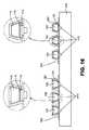
図12A〜図12Bは、本発明の一実施形態に係るキャリア基板201及びマイクロLED構造体アレイについて説明する平面図、並びに、断面側面図である。図示の特定の実施形態において、アレイは、マイクロp−nダイオード150を含む実施例10BNのマイクロLED構造体から作製されている。だが、図12A〜図12Bは、例示目的であり、マイクロLED構造体アレイは、前述のマイクロLED構造体アレイのいずれからも形成できることを、理解するべきである。図12Aで説明する実施形態では、各マイクロp−nダイオード150は、マイクロp−nダイオード150の最上面及び底面、並びに、最上面と底面との間に広がる先細形状の側壁の種々の幅に対応する種々の半径、又は幅を有する1組の同心円として示している。図12Bで説明する実施形態では、各マイクロp−nダイオード150は、先細又は角を丸めた1組の同心状正方形として示しており、各正方形は、マイクロp−nダイオード150の最上面及び底面、並びに、最上面と底面との間に広がる先細形状の側壁の種々の幅に対応した別々の幅を有する。だが、本発明の実施形態は、先細形状の側壁を必要とせず、マイクロp−nダイオード150の最上面及び底面は、同じ直径、又は幅で、並びに、垂直な側壁を有してもよい。図12A〜図12Bで示すように、マイクロLED構造体アレイは、ピッチ(P)、各マイクロLED構造体同士の間隔(S)及び各マイクロLED構造体の最大幅(W)を有するものとして、記載されている。明瞭さ及び簡潔さのために、この平面図では、x次元のみを点線で示しているが、同様のy次元も存在すると理解されたい。y次元には、同じ、又は異なる寸法値を持たせてもよい。図12A〜図12Bで示した特定の実施形態では、x次元及びy次元の値は、この平面図において同一である。一実施形態では、マイクロLED構造体アレイは、ピッチ(P)が10μmでよく、各マイクロLED構造体は、間隔(S)が2μmであり、最大幅(W)が8μmでよい。別の実施形態では、マイクロLED構造体アレイは、ピッチ(P)が5μmでよく、各マイクロLED構造体は、間隔(S)が2μmであり、最大幅(W)が3μmでよい。だが、本発明の実施形態は、これらの限定的な寸法に制限されず、適切な任意の寸法も利用可能である。 12A to 12B are a plan view and a cross-sectional side view for explaining the
マイクロLED構造体を転写先基板に転写する方法に関する実施形態を、図13において説明する。このような実施形態では、マイクロLED構造体アレイを上に配置したキャリア基板を提供している。前述のように、各マイクロLED構造体は、マイクロp−nダイオード及び金属層を含むことが可能であり、金属層は、マイクロp−nダイオードとキャリア基板上の接合層との間に配置される。共形誘電バリア層は、任意選択で、マイクロp−nダイオードの側壁に広がってもよい。更に、共形誘電バリア層は、マイクロp−nダイオードの底面の一部分、並びに、金属層及び接合層が存在すれば、その側壁にも広がってもよい。そして、操作1310で、少なくとも1つのマイクロLED構造体の接合層において、相転移を発生させる。例えば、この相転移は、接合層を形成する材料の融点若しくは液相線温度よりも高い温度で接合層を加熱する工程、又は接合層を形成する材料の結晶相に変化する工程に関連してもよい。次に、操作1320で、マイクロp−nダイオードと金属層、任意選択で、少なくとも1つのマイクロLED構造体における共形誘電バリア層の一部分、及び任意選択で接合層210の一部分を、転写ヘッドでピックアップしてから、操作1330で転写先基板に配置する。 An embodiment relating to a method for transferring a micro LED structure to a transfer destination substrate will be described with reference to FIG. In such an embodiment, a carrier substrate is provided having a micro LED structure array disposed thereon. As described above, each micro LED structure can include a micro pn diode and a metal layer, the metal layer being disposed between the micro pn diode and the junction layer on the carrier substrate. The The conformal dielectric barrier layer may optionally extend over the sidewalls of the micro pn diode. Furthermore, the conformal dielectric barrier layer may extend to a portion of the bottom surface of the micro pn diode and to the sidewalls of the metal layer and junction layer, if present. Then, in
実施形態に係る操作1320に関する一般的な説明を、図14において提供する。この操作では、転写ヘッド300が、マイクロp−nダイオード、金属層、少なくとも1つのマイクロLED構造体における共形誘電バリア層の一部分、及び接合層210の一部分をピックアップする。図示の特定の実施形態では、共形誘電バリア層を形成したが、他の実施形態では、共形誘電バリア層が存在しないこともある。いくつかの実施形態では、接合層の略半分などの接合層210の一部分を、マイクロLED構造体と共にリフトオフ可能である。マイクロp−nダイオード150を含む特定のマイクロLED構造体について説明しているが、本明細書で述べたマイクロp−nダイオード150のいずれを含むマイクロLED構造体のいずれを、ピックアップ可能であることを理解されたい。更に、図14で説明する実施形態は、1つのマイクロLED構造体をピックアップする転写ヘッド300を示しているが、他の実施形態では、転写ヘッド300は、一群のマイクロLED構造体をピックアップ可能である。 A general description of
更に、図14を参照すると、図示の特定の実施形態では、マイクロp−nダイオード150の底面は、金属層120の最上面よりも広く、共形誘電バリア層160は、マイクロp−nダイオード150の側壁、マイクロp−nダイオード150の底面の一部分、及び金属層120の側壁に広がる。これは、マイクロp−nダイオード135にも適用可能である。一態様において、マイクロp−nダイオード135、150より下方を覆う共形誘電バリア層160の部分は、マイクロp−nダイオード150の側壁上の共形誘電バリア層160を転写ヘッド300によるピックアップ操作中のチッピング、又は破断から保護する。金属層120、又は接合層210に隣接し、とりわけ、隅部及び鋭角を成す位置にある共形誘電バリア層160内で、応力点が生じ得る。マイクロLED構造体と転写ヘッド300との接触時、及び/又は、接合層中の相転移の発生時に、これらの応力点は、共形誘電バリア層160における自然な切断点となり、ここから共形誘電バリア層が切断できる。一実施形態では、マイクロLED構造体と転写ヘッドとの接触、及び/又は、接合層における相転移の発生の後に、共形誘電バリア層160が、この自然な切断点で切断される。この切断は、マイクロp−nダイオード及び金属層のピックアップの前又はその最中に起こりうる。前述のように、液体状態では、マイクロLED構造体と転写ヘッドとの接触に関連する圧縮力に反応して、接合層は、下部の構造体の上方に平滑化可能である。一実施形態では、マイクロLED構造体と転写ヘッドとの接触後、接合層中に相転移が発生する前に、転写ヘッドはマイクロLED構造体の最上面を摩擦する。摩擦することにより、転写ヘッド、又はマイクロLED構造体いずれかの接触面上に存在しうる任意の小片を取り除くことがある。更に、摩擦することにより、圧力を共形誘電バリア層に伝達することができる。したがって、転写ヘッド300から共形誘電バリア層までの圧力の伝達、及び接合層の液相線温度より高温での接合層の加熱は共に、マイクロp−nダイオード135、150の下側で共形誘電バリア層160を切断することに寄与し、マイクロLED構造体及び量子井戸層の完全性を維持できる。一実施形態では、マイクロp−nダイオード135、150の底面は、共形誘電バリア層160がマイクロp−nダイオード135、150の底面上で形成されるスペースがある程度まで、金属層120の最上面よりも広く、切断点を生成する。だが、この距離は、リソグラフィの公差によってでも決められる。一実施形態では、マイクロp−nダイオード135、150のそれぞれの側の0.25μmから1μmまでの距離は、厚さが50オングストロームから600オングストロームまでの共形誘電バリア層160に適合する。 Further, referring to FIG. 14, in the particular embodiment illustrated, the bottom surface of the
本発明の実施形態に係るピックアップ及び配置操作1320、1330を支援するために、種々の適切な転写ヘッドを利用できる。例えば、マイクロLED構造体をピックアップするために、転写ヘッド300は、真空、磁力、粘着、又は静電気原理に従って、ピックアップ圧力をマイクロLED構造体にもたらし得る。 A variety of suitable transfer heads can be utilized to assist with the pick and
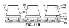
図15は、本発明の実施形態に従ってマイクロLED構造体をピックアップするために、静電原理に基づいて動作するバイポーラ型マイクロデバイス転写ヘッドの断面側面図である。図示のように、マイクロデバイス転写ヘッド300は、ベース基板302と、最上面308及び側壁306を持つメサ構造体304と、メサ構造体304の上に形成され、最上面309及び側壁307を含む任意のパッシベーション層310と、メサ構造体304(及び、任意選択のパッシベーション層310)上に形成された一対の電極316A及び316Bと、電極316A及び316Bを覆う最上面321を有する誘電体層320と、を含むことができる。ベース基板302は、構造担持を提供可能とするシリコン、セラミックス、及び高分子などの種々の材料から形成できる。一実施形態では、ベース基板は、103から1018Ω−cmまでの導電率を有する。ベース基板302は、マイクロデバイス転写ヘッド300を静電グリッパ装置の運転電子機器に接続する配線(図示せず)を、更に含むことが可能である。FIG. 15 is a cross-sectional side view of a bipolar microdevice transfer head that operates on the electrostatic principle to pick up a micro LED structure according to an embodiment of the present invention. As shown, the
図16は、本発明の実施形態に従って複数のマイクロLED構造体を配置した転写先基板400について説明する図である。例えば、転写先基板は、限定されないが、ディスプレイ基板、照明基板、トランジスタなどの機能デバイスを備えた基板、又は金属再配線付き基板が可能である。図示の特定の実施形態において、ドライバ接触部410の上方に、各マイクロLED構造体を配置できる。次に、共通の接触線420を、一連のマイクロp−nダイオード135、150の上方に形成可能である。図示のように、マイクロp−nダイオード135、150の先細形状の側壁は、連続した接触線を形成し易くする形状を提供することができる。一実施形態では、共通の接触線420を、一連の赤色発光、緑色発光、又は青色発光マイクロLEDの上方に形成できる。特定の実施形態では、インジウムスズ酸化物(ITO)などの透明接触材料から、共通の接触線420を形成できるであろう。一実施形態では、複数のマイクロLEDを、赤色発光マイクロLED、緑色発光マイクロLED及び青色発光マイクロLEDを含む3つのLEDからなるピクセル群に配列できる。 FIG. 16 is a diagram illustrating a
更に、図16を参照すると、本発明の実施形態に係るp−nダイオード135、150の拡大図が提供されている。一実施形態では、p−nダイオード135、150は、厚さが約0.1μm〜3μmの最上部のn型層114、厚さが約0.3μm未満の量子井戸層116(SQW又はMQWであり得る)、並びに、厚さが約0.1μm〜1μmの下側のp型層118を含むことができる。ある実施形態では、最上部のn型層114は、厚さが0.1μm〜6μmでよい(前述のバルク層112を含める、又は置き換えてもよい)。特定の実施形態では、p−nダイオード135、150は、厚さが3μm未満で、幅が10μm未満でよい。 Further, referring to FIG. 16, an enlarged view of
本発明の種々の態様を利用する際、ピックアップし転写先基板に転写するために準備されたマイクロLED構造体アレイを形成するために、上記実施形態の組合せ又は変形形態が実施可能であることが当業者には明らかであろう。本発明を構造特徴及び/又は方法論に特定されるような言葉で論じてきたが、添付の特許請求の範囲内で定義される本発明は、記載した特定の特徴又は行為に限定されるとは限らないと理解されたい。開示した特定の機能及び行為は、本発明を説明する上で有用な請求項に係る発明に関するとりわけ適切な実施形態として理解されよう。 When utilizing various aspects of the present invention, combinations or variations of the above embodiments may be possible to form a micro LED structure array that is prepared for pickup and transfer to a destination substrate. It will be apparent to those skilled in the art. Although the invention has been discussed in terms such as those specified in structural features and / or methodologies, the invention as defined in the appended claims is not limited to the specific features or acts described Please understand that it is not limited. The particular features and acts disclosed will be understood as particularly suitable embodiments of the claimed invention useful in describing the present invention.
Claims (30)
Translated fromJapaneseマイクロp−nダイオードと、
金属層と、を備え、
前記金属層が、前記マイクロp−nダイオードと基板上に形成された接合層との間にあり、前記接合層が、約350℃より低い液相線温度を有する、マイクロLED構造体。A micro LED structure,
A micro pn diode;
A metal layer,
A micro LED structure, wherein the metal layer is between the micro pn diode and a junction layer formed on a substrate, the junction layer having a liquidus temperature below about 350 ° C.
前記マイクロp−nダイオードの前記最上面の幅より広い幅、
前記マイクロp−nダイオードの前記最上面の前記幅より狭い幅、及び
前記マイクロp−nダイオードの前記最上面の前記幅とほぼ同じ幅からなる群から選択される幅を有する、請求項2に記載のマイクロLED構造体。The micro LED structure further includes an opening exposing the top surface of the micro pn diode in the conformal dielectric barrier layer, and the opening includes:
A width wider than the width of the top surface of the micro pn diode;
3. The width of the micro pn diode having a width selected from the group consisting of a width narrower than the width of the uppermost surface of the micro pn diode and substantially the same width as the width of the uppermost surface of the micro pn diode. The described micro LED structure.
前記金属層が、最上面及び底面を含み、
前記マイクロp−nダイオードの前記底面が、前記金属層の前記最上面よりも広い、請求項1に記載のマイクロLED構造体。The micro pn diode includes a top surface and a bottom surface;
The metal layer includes a top surface and a bottom surface;
The micro LED structure of claim 1, wherein the bottom surface of the micro pn diode is wider than the top surface of the metal layer.
前記接合層が、最上面及び底面を含み、
前記マイクロp−nダイオードの前記底面が、前記接合層の前記最上面よりも広い、請求項1に記載のマイクロLED構造体。The micro pn diode includes a top surface and a bottom surface;
The bonding layer includes a top surface and a bottom surface;
The micro LED structure according to claim 1, wherein the bottom surface of the micro pn diode is wider than the top surface of the bonding layer.
前記接合層が、最上面及び底面を含み、
前記マイクロp−nダイオードの前記底面が、前記接合層の前記最上面とほぼ同じ幅である、請求項1に記載のマイクロLED構造体。The micro pn diode includes a top surface and a bottom surface;
The bonding layer includes a top surface and a bottom surface;
The micro LED structure of claim 1, wherein the bottom surface of the micro pn diode is approximately the same width as the top surface of the junction layer.
基板上の接合層の複数の箇所と、
前記接合層の前記複数の箇所上の対応する複数のマイクロLED構造体と、を備え、
各マイクロLED構造体が、
マイクロp−nダイオードと、
金属層と、を含み、
前記金属層は、前記マイクロp−nダイオードと前記接合層の対応する箇所との間に配置される、マイクロLEDアレイ。A micro LED array,
Multiple locations of the bonding layer on the substrate;
A plurality of corresponding micro LED structures on the plurality of locations of the bonding layer,
Each micro LED structure is
A micro pn diode;
A metal layer,
The micro LED array, wherein the metal layer is disposed between the micro pn diode and a corresponding portion of the junction layer.
対応するマイクロp−nダイオードの前記最上面の幅よりも広い幅、
前記対応するマイクロp−nダイオードの前記最上面の前記幅よりも狭い幅、及び
対応するマイクロp−nダイオードの前記最上面の前記幅とほぼ同じ幅からなる群から選択される幅を有する、請求項17に記載のマイクロLED構造体。The conformal dielectric barrier layer further includes a plurality of openings exposing an uppermost surface of each micro pn diode, and each opening includes:
A width wider than the width of the top surface of the corresponding micro pn diode;
A width selected from the group consisting of a width narrower than the width of the top surface of the corresponding micro pn diode and a width substantially the same as the width of the top surface of the corresponding micro pn diode; The micro LED structure according to claim 17.
各金属層は、最上面及び底面を含み、
各マイクロp−nダイオードの前記底面は、前記金属層の前記対応する最上面よりも広い、請求項16に記載のマイクロLEDアレイ。Each micro pn diode includes a top surface and a bottom surface,
Each metal layer includes a top surface and a bottom surface,
17. The micro LED array of claim 16, wherein the bottom surface of each micro pn diode is wider than the corresponding top surface of the metal layer.
Applications Claiming Priority (11)
| Application Number | Priority Date | Filing Date | Title |
|---|---|---|---|
| US201161561706P | 2011-11-18 | 2011-11-18 | |
| US61/561,706 | 2011-11-18 | ||
| US201261594919P | 2012-02-03 | 2012-02-03 | |
| US61/594,919 | 2012-02-03 | ||
| US13/372,245US8426227B1 (en) | 2011-11-18 | 2012-02-13 | Method of forming a micro light emitting diode array |
| US13/372,222US8809875B2 (en) | 2011-11-18 | 2012-02-13 | Micro light emitting diode |
| US13/372,258US8794501B2 (en) | 2011-11-18 | 2012-02-13 | Method of transferring a light emitting diode |
| US13/372,258 | 2012-02-13 | ||
| US13/372,245 | 2012-02-13 | ||
| US13/372,222 | 2012-02-13 | ||
| PCT/US2012/064231WO2013074374A1 (en) | 2011-11-18 | 2012-11-08 | Micro light emitting diode |
Publications (1)
| Publication Number | Publication Date |
|---|---|
| JP2015500562Atrue JP2015500562A (en) | 2015-01-05 |
Family
ID=48094811
Family Applications (1)
| Application Number | Title | Priority Date | Filing Date |
|---|---|---|---|
| JP2014542349APendingJP2015500562A (en) | 2011-11-18 | 2012-11-08 | Micro light emitting diode |
Country Status (10)
| Country | Link |
|---|---|
| US (7) | US8794501B2 (en) |
| EP (1) | EP2780953B1 (en) |
| JP (1) | JP2015500562A (en) |
| KR (2) | KR101704152B1 (en) |
| CN (2) | CN104094422B (en) |
| AU (2) | AU2012339942B2 (en) |
| BR (1) | BR112014011802A2 (en) |
| MX (1) | MX340348B (en) |
| TW (4) | TWI566433B (en) |
| WO (3) | WO2013074374A1 (en) |
Cited By (35)
| Publication number | Priority date | Publication date | Assignee | Title |
|---|---|---|---|---|
| JP2016213441A (en)* | 2015-04-30 | 2016-12-15 | ミクロ メサ テクノロジー カンパニー リミテッド | Micro light-emitting diode |
| JP2016213353A (en)* | 2015-05-11 | 2016-12-15 | 株式会社ディスコ | Chuck table |
| JP2016219780A (en)* | 2015-05-21 | 2016-12-22 | ミクロ メサ テクノロジー カンパニー リミテッド | Micro light emitting diode |
| JP2017502511A (en)* | 2013-12-17 | 2017-01-19 | フォルシュングスフェアブント ベルリン エー ファウForschungsverbund Berlin e.V. | Method for forming a metal contact on the surface of a semiconductor and apparatus comprising the metal contact |
| JP2017537476A (en)* | 2015-04-01 | 2017-12-14 | ゴルテック.インク | Micro light emitting diode transfer method, manufacturing method, apparatus, and electronic apparatus |
| JP2017537475A (en)* | 2015-05-21 | 2017-12-14 | ゴルテック.インク | Micro light-emitting diode transport method, manufacturing method, apparatus, and electronic apparatus |
| JP2017539088A (en)* | 2015-08-18 | 2017-12-28 | ゴルテック.インク | Micro light-emitting diode repair method, manufacturing method, apparatus, and electronic apparatus |
| US9887184B2 (en) | 2015-07-23 | 2018-02-06 | Seoul Semiconductor Co., Ltd. | Display apparatus and manufacturing method thereof |
| JP2018506166A (en)* | 2015-08-18 | 2018-03-01 | ゴルテック.インク | Pre-exclusion method, manufacturing method, apparatus and electronic apparatus for micro light-emitting diode |
| US9978727B2 (en) | 2016-02-26 | 2018-05-22 | Seoul Semiconductor Co., Ltd. | Display apparatus and manufacturing method thereof |
| US9997688B2 (en) | 2016-02-26 | 2018-06-12 | Seoul Semiconducter Co., Ltd. | Display apparatus and manufacturing method thereof |
| US10068884B2 (en) | 2016-04-01 | 2018-09-04 | Seoul Semiconductor Co., Ltd. | Display apparatus and manufacturing method thereof |
| KR20180130312A (en)* | 2017-05-29 | 2018-12-07 | 엘지전자 주식회사 | Lamp for vehicle and vehicle |
| KR20180134682A (en)* | 2017-06-09 | 2018-12-19 | 엘지전자 주식회사 | Lamp for vehicle and vehicle |
| KR20190008746A (en) | 2017-07-17 | 2019-01-25 | 서울반도체 주식회사 | Display apparatus |
| KR20190014430A (en) | 2017-08-02 | 2019-02-12 | 서울반도체 주식회사 | Manufacturing method of display apparatus and manufacturing apparatus thereof |
| KR20190068420A (en)* | 2017-12-08 | 2019-06-18 | 신에쓰 가가꾸 고교 가부시끼가이샤 | Adhesive substrate and method for producing adhesive substrate |
| US10332949B2 (en) | 2016-07-06 | 2019-06-25 | Seoul Semiconductor Co., Ltd. | Display apparatus |
| JP2019140400A (en)* | 2019-04-08 | 2019-08-22 | ゴルテック.インク | Pre-screening method, manufacturing method, device, and electronic apparatus of micro light emitting diode |
| WO2019176409A1 (en) | 2018-03-13 | 2019-09-19 | 富士フイルム株式会社 | Method for manufacturing cured film, and method for manufacturing solid-state imaging element |
| US10606121B2 (en) | 2016-09-12 | 2020-03-31 | Seoul Semiconductor Co., Ltd. | Display apparatus |
| WO2021024722A1 (en)* | 2019-08-02 | 2021-02-11 | 株式会社ジャパンディスプレイ | Display device |
| KR20210085979A (en)* | 2019-12-31 | 2021-07-08 | 주식회사 에이맵플러스 | Light source module, display panel and manufacturing method thereof |
| JP2021118327A (en)* | 2020-01-29 | 2021-08-10 | 日亜化学工業株式会社 | Manufacturing method of light emitting device |
| US11139342B2 (en) | 2018-09-26 | 2021-10-05 | Nitride Semiconductors Co., Ltd. | UV-LED and display |
| JP2022073007A (en)* | 2020-10-30 | 2022-05-17 | 信越化学工業株式会社 | Manufacturing method of light emitting diode supply board, manufacturing method of light emitting diode display, manufacturing method of split unit for light emitting diode display, and manufacturing method of element supply board |
| WO2022210175A1 (en) | 2021-03-29 | 2022-10-06 | 富士フイルム株式会社 | Black photosensitive composition, manufacturing method of black photosensitive composition, cured film, color filter, light-shielding film, optical element, solid-state image capturing element, and headlight unit |
| JP2023526534A (en)* | 2020-05-22 | 2023-06-21 | プレッシー・セミコンダクターズ・リミテッド | light emitting device array |
| KR20230109182A (en) | 2021-03-26 | 2023-07-19 | 데쿠세리아루즈 가부시키가이샤 | filler array film |
| KR20230127298A (en) | 2021-03-26 | 2023-08-31 | 데쿠세리아루즈 가부시키가이샤 | filler array film |
| JP2023172546A (en)* | 2022-05-24 | 2023-12-06 | 日亜化学工業株式会社 | Method for manufacturing light-emitting device |
| WO2024034480A1 (en)* | 2022-08-10 | 2024-02-15 | 信越半導体株式会社 | Method for producing bonded wafer for micro leds |
| KR20240123431A (en) | 2022-03-31 | 2024-08-13 | 데쿠세리아루즈 가부시키가이샤 | Connection structure |
| KR20250036212A (en) | 2022-09-28 | 2025-03-13 | 데쿠세리아루즈 가부시키가이샤 | Connection structure |
| KR20250036210A (en) | 2022-09-28 | 2025-03-13 | 데쿠세리아루즈 가부시키가이샤 | Connection structure |
Families Citing this family (331)
| Publication number | Priority date | Publication date | Assignee | Title |
|---|---|---|---|---|
| DE102008054288A1 (en)* | 2008-11-03 | 2010-05-06 | Osram Gesellschaft mit beschränkter Haftung | Method for producing a flexible light strip |
| WO2010091391A2 (en) | 2009-02-09 | 2010-08-12 | Semprius, Inc. | Concentrator-type photovoltaic (cpv) modules, receivers and sub-receivers and methods of forming same |
| WO2010111601A2 (en) | 2009-03-26 | 2010-09-30 | Semprius, Inc. | Methods of forming printable integrated circuit devices and devices formed thereby |
| US9161448B2 (en) | 2010-03-29 | 2015-10-13 | Semprius, Inc. | Laser assisted transfer welding process |
| WO2012027458A1 (en) | 2010-08-26 | 2012-03-01 | Semprius, Inc. | Structures and methods for testing printable integrated circuits |
| US9899329B2 (en) | 2010-11-23 | 2018-02-20 | X-Celeprint Limited | Interconnection structures and methods for transfer-printed integrated circuit elements with improved interconnection alignment tolerance |
| US8889485B2 (en) | 2011-06-08 | 2014-11-18 | Semprius, Inc. | Methods for surface attachment of flipped active componenets |
| US9412727B2 (en) | 2011-09-20 | 2016-08-09 | Semprius, Inc. | Printing transferable components using microstructured elastomeric surfaces with pressure modulated reversible adhesion |
| US8349116B1 (en) | 2011-11-18 | 2013-01-08 | LuxVue Technology Corporation | Micro device transfer head heater assembly and method of transferring a micro device |
| US8573469B2 (en) | 2011-11-18 | 2013-11-05 | LuxVue Technology Corporation | Method of forming a micro LED structure and array of micro LED structures with an electrically insulating layer |
| US8794501B2 (en) | 2011-11-18 | 2014-08-05 | LuxVue Technology Corporation | Method of transferring a light emitting diode |
| US8333860B1 (en) | 2011-11-18 | 2012-12-18 | LuxVue Technology Corporation | Method of transferring a micro device |
| US10115862B2 (en) | 2011-12-27 | 2018-10-30 | eLux Inc. | Fluidic assembly top-contact LED disk |
| US9548332B2 (en)* | 2012-04-27 | 2017-01-17 | Apple Inc. | Method of forming a micro LED device with self-aligned metallization stack |
| US9105492B2 (en) | 2012-05-08 | 2015-08-11 | LuxVue Technology Corporation | Compliant micro device transfer head |
| US9034754B2 (en) | 2012-05-25 | 2015-05-19 | LuxVue Technology Corporation | Method of forming a micro device transfer head with silicon electrode |
| US8569115B1 (en) | 2012-07-06 | 2013-10-29 | LuxVue Technology Corporation | Method of forming a compliant bipolar micro device transfer head with silicon electrodes |
| US8415768B1 (en) | 2012-07-06 | 2013-04-09 | LuxVue Technology Corporation | Compliant monopolar micro device transfer head with silicon electrode |
| US8933433B2 (en) | 2012-07-30 | 2015-01-13 | LuxVue Technology Corporation | Method and structure for receiving a micro device |
| US9557215B2 (en) | 2012-08-17 | 2017-01-31 | Massachusetts Institute Of Technology | Phonon-recyling light-emitting diodes |
| US8791530B2 (en) | 2012-09-06 | 2014-07-29 | LuxVue Technology Corporation | Compliant micro device transfer head with integrated electrode leads |
| US9162880B2 (en) | 2012-09-07 | 2015-10-20 | LuxVue Technology Corporation | Mass transfer tool |
| US8941215B2 (en)* | 2012-09-24 | 2015-01-27 | LuxVue Technology Corporation | Micro device stabilization post |
| US8835940B2 (en) | 2012-09-24 | 2014-09-16 | LuxVue Technology Corporation | Micro device stabilization post |
| KR20140044103A (en)* | 2012-10-04 | 2014-04-14 | 삼성디스플레이 주식회사 | Organic light emitting diode display and method for manufacturing the same |
| US9558721B2 (en) | 2012-10-15 | 2017-01-31 | Apple Inc. | Content-based adaptive refresh schemes for low-power displays |
| US20140151630A1 (en)* | 2012-12-04 | 2014-06-05 | Feng-Hsu Fan | Protection for the epitaxial structure of metal devices |
| US9029880B2 (en) | 2012-12-10 | 2015-05-12 | LuxVue Technology Corporation | Active matrix display panel with ground tie lines |
| US9236815B2 (en) | 2012-12-10 | 2016-01-12 | LuxVue Technology Corporation | Compliant micro device transfer head array with metal electrodes |
| US9178123B2 (en) | 2012-12-10 | 2015-11-03 | LuxVue Technology Corporation | Light emitting device reflective bank structure |
| US9159700B2 (en) | 2012-12-10 | 2015-10-13 | LuxVue Technology Corporation | Active matrix emissive micro LED display |
| US9391042B2 (en) | 2012-12-14 | 2016-07-12 | Apple Inc. | Micro device transfer system with pivot mount |
| US9314930B2 (en) | 2012-12-14 | 2016-04-19 | LuxVue Technology Corporation | Micro pick up array with integrated pivot mount |
| US9308649B2 (en) | 2013-02-25 | 2016-04-12 | LuxVue Techonology Corporation | Mass transfer tool manipulator assembly |
| US9252375B2 (en) | 2013-03-15 | 2016-02-02 | LuxVue Technology Corporation | Method of fabricating a light emitting diode display with integrated defect detection test |
| US8791474B1 (en) | 2013-03-15 | 2014-07-29 | LuxVue Technology Corporation | Light emitting diode display with redundancy scheme |
| US9484504B2 (en) | 2013-05-14 | 2016-11-01 | Apple Inc. | Micro LED with wavelength conversion layer |
| US9136161B2 (en) | 2013-06-04 | 2015-09-15 | LuxVue Technology Corporation | Micro pick up array with compliant contact |
| EP3008553B1 (en) | 2013-06-12 | 2023-06-07 | Rohinni, Inc. | Keyboard backlighting with deposited light-generating sources |
| US8987765B2 (en) | 2013-06-17 | 2015-03-24 | LuxVue Technology Corporation | Reflective bank structure and method for integrating a light emitting device |
| US8928021B1 (en) | 2013-06-18 | 2015-01-06 | LuxVue Technology Corporation | LED light pipe |
| US9111464B2 (en) | 2013-06-18 | 2015-08-18 | LuxVue Technology Corporation | LED display with wavelength conversion layer |
| US9035279B2 (en)* | 2013-07-08 | 2015-05-19 | LuxVue Technology Corporation | Micro device with stabilization post |
| US9087764B2 (en) | 2013-07-26 | 2015-07-21 | LuxVue Technology Corporation | Adhesive wafer bonding with controlled thickness variation |
| EP3033776A4 (en) | 2013-08-16 | 2017-01-25 | Massachusetts Institute of Technology | Thermo-electrically pumped light-emitting diodes |
| US9153548B2 (en) | 2013-09-16 | 2015-10-06 | Lux Vue Technology Corporation | Adhesive wafer bonding with sacrificial spacers for controlled thickness variation |
| US9367094B2 (en) | 2013-12-17 | 2016-06-14 | Apple Inc. | Display module and system applications |
| US9768345B2 (en) | 2013-12-20 | 2017-09-19 | Apple Inc. | LED with current injection confinement trench |
| US9450147B2 (en) | 2013-12-27 | 2016-09-20 | Apple Inc. | LED with internally confined current injection area |
| US9583466B2 (en) | 2013-12-27 | 2017-02-28 | Apple Inc. | Etch removal of current distribution layer for LED current confinement |
| US9542638B2 (en) | 2014-02-18 | 2017-01-10 | Apple Inc. | RFID tag and micro chip integration design |
| US9583533B2 (en) | 2014-03-13 | 2017-02-28 | Apple Inc. | LED device with embedded nanowire LEDs |
| US9522468B2 (en) | 2014-05-08 | 2016-12-20 | Apple Inc. | Mass transfer tool manipulator assembly with remote center of compliance |
| US10229630B2 (en) | 2014-05-14 | 2019-03-12 | The Hong Kong University Of Science And Technology | Passive-matrix light-emitting diodes on silicon micro-display |
| US9318475B2 (en) | 2014-05-15 | 2016-04-19 | LuxVue Technology Corporation | Flexible display and method of formation with sacrificial release layer |
| US9741286B2 (en) | 2014-06-03 | 2017-08-22 | Apple Inc. | Interactive display panel with emitting and sensing diodes |
| US9624100B2 (en) | 2014-06-12 | 2017-04-18 | Apple Inc. | Micro pick up array pivot mount with integrated strain sensing elements |
| US9425151B2 (en) | 2014-06-17 | 2016-08-23 | Apple Inc. | Compliant electrostatic transfer head with spring support layer |
| US9570002B2 (en) | 2014-06-17 | 2017-02-14 | Apple Inc. | Interactive display panel with IR diodes |
| WO2015193436A1 (en) | 2014-06-18 | 2015-12-23 | X-Celeprint Limited | Systems and methods for preparing gan and related materials for micro assembly |
| US9865600B2 (en) | 2014-06-18 | 2018-01-09 | X-Celeprint Limited | Printed capacitors |
| TWI697057B (en) | 2014-06-18 | 2020-06-21 | 愛爾蘭商艾克斯展示公司技術有限公司 | Systems and methods for controlling release of transferable semiconductor structures |
| US10050351B2 (en) | 2014-06-18 | 2018-08-14 | X-Celeprint Limited | Multilayer printed capacitors |
| US9929053B2 (en) | 2014-06-18 | 2018-03-27 | X-Celeprint Limited | Systems and methods for controlling release of transferable semiconductor structures |
| US9444015B2 (en) | 2014-06-18 | 2016-09-13 | X-Celeprint Limited | Micro assembled LED displays and lighting elements |
| US9358775B2 (en) | 2014-07-20 | 2016-06-07 | X-Celeprint Limited | Apparatus and methods for micro-transfer-printing |
| US10739882B2 (en) | 2014-08-06 | 2020-08-11 | Apple Inc. | Electronic device display with array of discrete light-emitting diodes |
| JP7071118B2 (en)* | 2014-08-19 | 2022-05-18 | ルミレッズ ホールディング ベーフェー | Sapphire collector to reduce mechanical damage during die-level laser lift-off |
| WO2016030422A1 (en) | 2014-08-26 | 2016-03-03 | X-Celeprint Limited | Micro assembled hybrid displays and lighting elements |
| US9468050B1 (en) | 2014-09-25 | 2016-10-11 | X-Celeprint Limited | Self-compensating circuit for faulty display pixels |
| US9991163B2 (en) | 2014-09-25 | 2018-06-05 | X-Celeprint Limited | Small-aperture-ratio display with electrical component |
| US9799261B2 (en) | 2014-09-25 | 2017-10-24 | X-Celeprint Limited | Self-compensating circuit for faulty display pixels |
| US9799719B2 (en) | 2014-09-25 | 2017-10-24 | X-Celeprint Limited | Active-matrix touchscreen |
| US9818725B2 (en) | 2015-06-01 | 2017-11-14 | X-Celeprint Limited | Inorganic-light-emitter display with integrated black matrix |
| US9537069B1 (en) | 2014-09-25 | 2017-01-03 | X-Celeprint Limited | Inorganic light-emitting diode with encapsulating reflector |
| KR102271817B1 (en) | 2014-09-26 | 2021-07-01 | 삼성전자주식회사 | Smart contact lens for augmented reality and methods of manufacturing and operating the same |
| US9705432B2 (en) | 2014-09-30 | 2017-07-11 | Apple Inc. | Micro pick up array pivot mount design for strain amplification |
| US9828244B2 (en) | 2014-09-30 | 2017-11-28 | Apple Inc. | Compliant electrostatic transfer head with defined cavity |
| US10381332B2 (en) | 2014-10-31 | 2019-08-13 | eLux Inc. | Fabrication method for emissive display with light management system |
| US10446728B2 (en) | 2014-10-31 | 2019-10-15 | eLux, Inc. | Pick-and remove system and method for emissive display repair |
| US9985190B2 (en) | 2016-05-18 | 2018-05-29 | eLux Inc. | Formation and structure of post enhanced diodes for orientation control |
| US9825202B2 (en) | 2014-10-31 | 2017-11-21 | eLux, Inc. | Display with surface mount emissive elements |
| US10242977B2 (en) | 2014-10-31 | 2019-03-26 | eLux, Inc. | Fluid-suspended microcomponent harvest, distribution, and reclamation |
| US10319878B2 (en) | 2014-10-31 | 2019-06-11 | eLux, Inc. | Stratified quantum dot phosphor structure |
| US10249599B2 (en) | 2016-06-29 | 2019-04-02 | eLux, Inc. | Laminated printed color conversion phosphor sheets |
| US10381335B2 (en) | 2014-10-31 | 2019-08-13 | ehux, Inc. | Hybrid display using inorganic micro light emitting diodes (uLEDs) and organic LEDs (OLEDs) |
| US9892944B2 (en) | 2016-06-23 | 2018-02-13 | Sharp Kabushiki Kaisha | Diodes offering asymmetric stability during fluidic assembly |
| US10520769B2 (en) | 2014-10-31 | 2019-12-31 | eLux, Inc. | Emissive display with printed light modification structures |
| US10418527B2 (en) | 2014-10-31 | 2019-09-17 | eLux, Inc. | System and method for the fluidic assembly of emissive displays |
| US9755110B1 (en) | 2016-07-27 | 2017-09-05 | Sharp Laboratories Of America, Inc. | Substrate with topological features for steering fluidic assembly LED disks |
| US9722145B2 (en) | 2015-06-24 | 2017-08-01 | Sharp Laboratories Of America, Inc. | Light emitting device and fluidic manufacture thereof |
| US10236279B2 (en) | 2014-10-31 | 2019-03-19 | eLux, Inc. | Emissive display with light management system |
| US10535640B2 (en) | 2014-10-31 | 2020-01-14 | eLux Inc. | System and method for the fluidic assembly of micro-LEDs utilizing negative pressure |
| US9917226B1 (en) | 2016-09-15 | 2018-03-13 | Sharp Kabushiki Kaisha | Substrate features for enhanced fluidic assembly of electronic devices |
| US10543486B2 (en) | 2014-10-31 | 2020-01-28 | eLux Inc. | Microperturbation assembly system and method |
| US9773711B2 (en) | 2014-12-01 | 2017-09-26 | Industrial Technology Research Institute | Picking-up and placing process for electronic devices and electronic module |
| US9607907B2 (en) | 2014-12-01 | 2017-03-28 | Industrial Technology Research Institute | Electric-programmable magnetic module and picking-up and placement process for electronic devices |
| US9478583B2 (en) | 2014-12-08 | 2016-10-25 | Apple Inc. | Wearable display having an array of LEDs on a conformable silicon substrate |
| KR102322842B1 (en) | 2014-12-26 | 2021-11-08 | 엘지이노텍 주식회사 | Light emitting device array |
| US9633883B2 (en) | 2015-03-20 | 2017-04-25 | Rohinni, LLC | Apparatus for transfer of semiconductor devices |
| KR101614370B1 (en) | 2015-04-07 | 2016-04-21 | 엘지전자 주식회사 | Semiconductor light emitting device, transfer head of the semiconductor light emitting device, and method for transferring the semiconductor light emitting device |
| EP3295479B1 (en)* | 2015-05-13 | 2018-09-26 | Lumileds Holding B.V. | Sapphire collector for reducing mechanical damage during die level laser lift-off |
| TWI557831B (en)* | 2015-05-15 | 2016-11-11 | 友達光電股份有限公司 | Micro component transfer method |
| US9640715B2 (en) | 2015-05-15 | 2017-05-02 | X-Celeprint Limited | Printable inorganic semiconductor structures |
| US9871345B2 (en) | 2015-06-09 | 2018-01-16 | X-Celeprint Limited | Crystalline color-conversion device |
| US10102794B2 (en) | 2015-06-09 | 2018-10-16 | X-Celeprint Limited | Distributed charge-pump power-supply system |
| US10133426B2 (en) | 2015-06-18 | 2018-11-20 | X-Celeprint Limited | Display with micro-LED front light |
| US11061276B2 (en) | 2015-06-18 | 2021-07-13 | X Display Company Technology Limited | Laser array display |
| CN105493298B (en) | 2015-07-14 | 2018-06-12 | 歌尔股份有限公司 | Transfer method, manufacturing method, device and the electronic equipment of micro- light emitting diode |
| US10224308B2 (en) | 2015-07-14 | 2019-03-05 | Goertek, Inc. | Transferring method, manufacturing method, device and electronic apparatus of micro-LED |
| US9704821B2 (en) | 2015-08-11 | 2017-07-11 | X-Celeprint Limited | Stamp with structured posts |
| US10255834B2 (en) | 2015-07-23 | 2019-04-09 | X-Celeprint Limited | Parallel redundant chiplet system for controlling display pixels |
| US10468363B2 (en) | 2015-08-10 | 2019-11-05 | X-Celeprint Limited | Chiplets with connection posts |
| US9640108B2 (en) | 2015-08-25 | 2017-05-02 | X-Celeprint Limited | Bit-plane pulse width modulated digital display system |
| US10380930B2 (en) | 2015-08-24 | 2019-08-13 | X-Celeprint Limited | Heterogeneous light emitter display system |
| GB2549734B (en) | 2016-04-26 | 2020-01-01 | Facebook Tech Llc | A display |
| GB2545155B (en)* | 2015-09-02 | 2020-04-01 | Facebook Tech Llc | Assembly of semiconductor devices |
| GB2541970B (en) | 2015-09-02 | 2020-08-19 | Facebook Tech Llc | Display manufacture |
| US10600823B2 (en) | 2015-09-02 | 2020-03-24 | Facebook Technologies, Llc | Assembly of semiconductor devices |
| GB2544728B (en) | 2015-11-17 | 2020-08-19 | Facebook Tech Llc | Redundancy in inorganic light emitting diode displays |
| WO2017037475A1 (en)* | 2015-09-02 | 2017-03-09 | Oculus Vr, Llc | Assembly of semiconductor devices |
| US10304811B2 (en) | 2015-09-04 | 2019-05-28 | Hong Kong Beida Jade Bird Display Limited | Light-emitting diode display panel with micro lens array |
| US10032757B2 (en) | 2015-09-04 | 2018-07-24 | Hong Kong Beida Jade Bird Display Limited | Projection display system |
| US10177127B2 (en) | 2015-09-04 | 2019-01-08 | Hong Kong Beida Jade Bird Display Limited | Semiconductor apparatus and method of manufacturing the same |
| CN105108417B (en)* | 2015-09-17 | 2016-10-05 | 贵州雅光电子科技股份有限公司 | A kind of diode welding mould and using method thereof |
| US10217402B1 (en)* | 2015-09-25 | 2019-02-26 | Apple Inc. | Driving circuitry for micro light emitting diode electronic displays |
| US10230048B2 (en) | 2015-09-29 | 2019-03-12 | X-Celeprint Limited | OLEDs for micro transfer printing |
| US10418501B2 (en) | 2015-10-02 | 2019-09-17 | X-Celeprint Limited | Wafer-integrated, ultra-low profile concentrated photovoltaics (CPV) for space applications |
| EP3262694B1 (en) | 2015-10-20 | 2019-08-21 | Goertek. Inc | Method for transferring micro-leds and method for manufacturing micro-led device |
| CN105723528A (en) | 2015-11-04 | 2016-06-29 | 歌尔声学股份有限公司 | Transfer method, manufacturing method, device and electronic equipment of micro light emitting diode |
| KR102427644B1 (en) | 2015-11-16 | 2022-08-02 | 삼성전자주식회사 | Light source, method of manufacturing the same, and display apparatus having the same |
| TWI555241B (en)* | 2015-11-19 | 2016-10-21 | Jin-Ywan Lin | A light emitting diode array structure |
| KR20170059068A (en) | 2015-11-19 | 2017-05-30 | 삼성전자주식회사 | Lighting source module, display panel and display apparatus |
| KR102546307B1 (en) | 2015-12-02 | 2023-06-21 | 삼성전자주식회사 | Light emitting device and display device including the same |
| TWI563490B (en) | 2015-12-04 | 2016-12-21 | Ind Tech Res Inst | Display pixel and display panel |
| US10066819B2 (en) | 2015-12-09 | 2018-09-04 | X-Celeprint Limited | Micro-light-emitting diode backlight system |
| US10091446B2 (en) | 2015-12-23 | 2018-10-02 | X-Celeprint Limited | Active-matrix displays with common pixel control |
| WO2017107097A1 (en)* | 2015-12-23 | 2017-06-29 | Goertek.Inc | Micro-led transfer method and manufacturing method |
| US9930277B2 (en) | 2015-12-23 | 2018-03-27 | X-Celeprint Limited | Serial row-select matrix-addressed system |
| US9786646B2 (en) | 2015-12-23 | 2017-10-10 | X-Celeprint Limited | Matrix addressed device repair |
| US9928771B2 (en) | 2015-12-24 | 2018-03-27 | X-Celeprint Limited | Distributed pulse width modulation control |
| JP6959697B2 (en) | 2016-01-15 | 2021-11-05 | ロヒンニ リミテッド ライアビリティ カンパニー | Devices and methods that are backlit through a cover on the device |
| US10923023B1 (en) | 2016-01-26 | 2021-02-16 | Apple Inc. | Stacked hybrid micro LED pixel architecture |
| US11230471B2 (en) | 2016-02-05 | 2022-01-25 | X-Celeprint Limited | Micro-transfer-printed compound sensor device |
| US10361677B2 (en) | 2016-02-18 | 2019-07-23 | X-Celeprint Limited | Transverse bulk acoustic wave filter |
| US10200013B2 (en) | 2016-02-18 | 2019-02-05 | X-Celeprint Limited | Micro-transfer-printed acoustic wave filter device |
| EP3208028B1 (en)* | 2016-02-19 | 2021-04-07 | Max-Planck-Gesellschaft zur Förderung der Wissenschaften e.V. | A method and device for reversibly attaching a phase changing metal to an object |
| US10109753B2 (en) | 2016-02-19 | 2018-10-23 | X-Celeprint Limited | Compound micro-transfer-printed optical filter device |
| DE102016103324A1 (en)* | 2016-02-25 | 2017-08-31 | Osram Opto Semiconductors Gmbh | Video wall module and method of making a video wall module |
| TWI710061B (en) | 2016-02-25 | 2020-11-11 | 愛爾蘭商艾克斯展示公司技術有限公司 | Efficiently micro-transfer printing micro-scale devices onto large-format substrates |
| US10150326B2 (en) | 2016-02-29 | 2018-12-11 | X-Celeprint Limited | Hybrid document with variable state |
| US10150325B2 (en) | 2016-02-29 | 2018-12-11 | X-Celeprint Limited | Hybrid banknote with electronic indicia |
| US10193025B2 (en) | 2016-02-29 | 2019-01-29 | X-Celeprint Limited | Inorganic LED pixel structure |
| US10153257B2 (en) | 2016-03-03 | 2018-12-11 | X-Celeprint Limited | Micro-printed display |
| US10153256B2 (en) | 2016-03-03 | 2018-12-11 | X-Celeprint Limited | Micro-transfer printable electronic component |
| US10917953B2 (en) | 2016-03-21 | 2021-02-09 | X Display Company Technology Limited | Electrically parallel fused LEDs |
| US10103069B2 (en) | 2016-04-01 | 2018-10-16 | X-Celeprint Limited | Pressure-activated electrical interconnection by micro-transfer printing |
| US10008483B2 (en) | 2016-04-05 | 2018-06-26 | X-Celeprint Limited | Micro-transfer printed LED and color filter structure |
| US10199546B2 (en) | 2016-04-05 | 2019-02-05 | X-Celeprint Limited | Color-filter device |
| TWI581417B (en)* | 2016-04-11 | 2017-05-01 | 友達光電股份有限公司 | Light emitting apparatus and fabricating method thereof |
| CN105679196A (en)* | 2016-04-11 | 2016-06-15 | 深圳市丽格特光电有限公司 | Full-color high-resolution micro-display chip based on gallium nitride LEDs and quantum dot technology |
| US10198890B2 (en) | 2016-04-19 | 2019-02-05 | X-Celeprint Limited | Hybrid banknote with electronic indicia using near-field-communications |
| US9997102B2 (en) | 2016-04-19 | 2018-06-12 | X-Celeprint Limited | Wirelessly powered display and system |
| US10360846B2 (en) | 2016-05-10 | 2019-07-23 | X-Celeprint Limited | Distributed pulse-width modulation system with multi-bit digital storage and output device |
| US10622700B2 (en) | 2016-05-18 | 2020-04-14 | X-Celeprint Limited | Antenna with micro-transfer-printed circuit element |
| US9997501B2 (en) | 2016-06-01 | 2018-06-12 | X-Celeprint Limited | Micro-transfer-printed light-emitting diode device |
| CN108698813B (en)* | 2016-06-02 | 2023-01-20 | 歌尔股份有限公司 | MEMS device and electronic equipment |
| CN108475685A (en)* | 2016-06-02 | 2018-08-31 | 歌尔股份有限公司 | Monolithic integrated device and micro-total analysis system |
| US10453826B2 (en) | 2016-06-03 | 2019-10-22 | X-Celeprint Limited | Voltage-balanced serial iLED pixel and display |
| US11137641B2 (en) | 2016-06-10 | 2021-10-05 | X Display Company Technology Limited | LED structure with polarized light emission |
| US9627437B1 (en) | 2016-06-30 | 2017-04-18 | Sharp Laboratories Of America, Inc. | Patterned phosphors in through hole via (THV) glass |
| US10475876B2 (en) | 2016-07-26 | 2019-11-12 | X-Celeprint Limited | Devices with a single metal layer |
| US10222698B2 (en) | 2016-07-28 | 2019-03-05 | X-Celeprint Limited | Chiplets with wicking posts |
| US11064609B2 (en) | 2016-08-04 | 2021-07-13 | X Display Company Technology Limited | Printable 3D electronic structure |
| US9997399B2 (en) | 2016-08-16 | 2018-06-12 | Mikro Mesa Technology Co., Ltd. | Method for transferring semiconductor structure |
| US10243097B2 (en) | 2016-09-09 | 2019-03-26 | eLux Inc. | Fluidic assembly using tunable suspension flow |
| CN107833526B (en)* | 2016-09-15 | 2021-05-28 | 伊乐视有限公司 | Pick-and-remove system and method of repairing illuminated displays |
| US9980341B2 (en) | 2016-09-22 | 2018-05-22 | X-Celeprint Limited | Multi-LED components |
| US10157880B2 (en) | 2016-10-03 | 2018-12-18 | X-Celeprint Limited | Micro-transfer printing with volatile adhesive layer |
| CN106356379A (en)* | 2016-10-28 | 2017-01-25 | 江苏新广联半导体有限公司 | GaN-based micro display chip architecture and production method |
| US10782002B2 (en) | 2016-10-28 | 2020-09-22 | X Display Company Technology Limited | LED optical components |
| US10353204B2 (en) | 2016-10-31 | 2019-07-16 | Tectus Corporation | Femtoprojector optical systems |
| US10141215B2 (en) | 2016-11-03 | 2018-11-27 | Rohinni, LLC | Compliant needle for direct transfer of semiconductor devices |
| CN107039298B (en)* | 2016-11-04 | 2019-12-24 | 厦门市三安光电科技有限公司 | Micro-component transfer device, transfer method, manufacturing method, device and electronic device |
| CN109891608B (en) | 2016-11-07 | 2021-10-08 | 歌尔股份有限公司 | Micro light emitting diode transfer method and manufacturing method |
| US9837390B1 (en) | 2016-11-07 | 2017-12-05 | Corning Incorporated | Systems and methods for creating fluidic assembly structures on a substrate |
| US10347168B2 (en) | 2016-11-10 | 2019-07-09 | X-Celeprint Limited | Spatially dithered high-resolution |
| EP3542394B1 (en) | 2016-11-15 | 2025-09-24 | X Display Company Technology Limited | Micro-transfer-printable flip-chip structures and manufacturing methods thereof |
| US10600671B2 (en) | 2016-11-15 | 2020-03-24 | X-Celeprint Limited | Micro-transfer-printable flip-chip structures and methods |
| US10395966B2 (en) | 2016-11-15 | 2019-08-27 | X-Celeprint Limited | Micro-transfer-printable flip-chip structures and methods |
| KR101874199B1 (en)* | 2016-11-23 | 2018-07-04 | 광주과학기술원 | Transfer Array of Micro Device based on Magnetic Induction and Method of transferring the Micro Device |
| US10504767B2 (en) | 2016-11-23 | 2019-12-10 | Rohinni, LLC | Direct transfer apparatus for a pattern array of semiconductor device die |
| US10471545B2 (en) | 2016-11-23 | 2019-11-12 | Rohinni, LLC | Top-side laser for direct transfer of semiconductor devices |
| KR20180060704A (en) | 2016-11-29 | 2018-06-07 | 광주과학기술원 | Micro-Display of having verically Stacking Structure and Method of forming the same |
| US10297502B2 (en) | 2016-12-19 | 2019-05-21 | X-Celeprint Limited | Isolation structure for micro-transfer-printable devices |
| US10438859B2 (en) | 2016-12-19 | 2019-10-08 | X-Celeprint Limited | Transfer printed device repair |
| US10832609B2 (en) | 2017-01-10 | 2020-11-10 | X Display Company Technology Limited | Digital-drive pulse-width-modulated output system |
| US10062588B2 (en) | 2017-01-18 | 2018-08-28 | Rohinni, LLC | Flexible support substrate for transfer of semiconductor devices |
| US10332868B2 (en) | 2017-01-26 | 2019-06-25 | X-Celeprint Limited | Stacked pixel structures |
| US10468391B2 (en) | 2017-02-08 | 2019-11-05 | X-Celeprint Limited | Inorganic light-emitting-diode displays with multi-ILED pixels |
| US12322732B2 (en)* | 2017-02-09 | 2025-06-03 | Vuereal Inc. | Circuit and system integration onto a microdevice substrate |
| US10396137B2 (en) | 2017-03-10 | 2019-08-27 | X-Celeprint Limited | Testing transfer-print micro-devices on wafer |
| US10937768B2 (en) | 2017-03-13 | 2021-03-02 | Seoul Semiconductor Co., Ltd. | Method of manufacturing display device |
| US10770440B2 (en) | 2017-03-15 | 2020-09-08 | Globalfoundries Inc. | Micro-LED display assembly |
| TWI756384B (en)* | 2017-03-16 | 2022-03-01 | 美商康寧公司 | Method and process for mass transfer of micro-leds |
| JP6918537B2 (en)* | 2017-03-24 | 2021-08-11 | 東レエンジニアリング株式会社 | Pickup method, pickup device, and mounting device |
| US11024608B2 (en) | 2017-03-28 | 2021-06-01 | X Display Company Technology Limited | Structures and methods for electrical connection of micro-devices and substrates |
| DE102017106755B4 (en) | 2017-03-29 | 2022-08-18 | OSRAM Opto Semiconductors Gesellschaft mit beschränkter Haftung | Method for producing an optoelectronic semiconductor component and optoelectronic semiconductor component |
| US10468397B2 (en) | 2017-05-05 | 2019-11-05 | X-Celeprint Limited | Matrix addressed tiles and arrays |
| CN106997745A (en)* | 2017-06-15 | 2017-08-01 | 京东方科技集团股份有限公司 | A kind of display device and its driving method |
| TWI613488B (en)* | 2017-06-19 | 2018-02-01 | 友達光電股份有限公司 | Display panel and method of forming micro component holder |
| KR102029533B1 (en) | 2017-07-04 | 2019-10-07 | 주식회사콘스탄텍 | Micro Light Emitting Diodes And Their Application For Full Color Display Device |
| CN109213360B (en)* | 2017-07-07 | 2021-12-24 | 鸿富锦精密工业(深圳)有限公司 | Miniature LED touch display panel |
| US10804880B2 (en) | 2018-12-03 | 2020-10-13 | X-Celeprint Limited | Device structures with acoustic wave transducers and connection posts |
| CN109216522B (en)* | 2017-07-07 | 2020-02-07 | 鸿富锦精密工业(深圳)有限公司 | Miniature LED display panel |
| US10431483B2 (en)* | 2017-07-14 | 2019-10-01 | Industrial Technology Research Institute | Transfer support and transfer module |
| US11227787B2 (en) | 2017-07-14 | 2022-01-18 | Industrial Technology Research Institute | Transfer support and transfer module |
| WO2019017924A1 (en)* | 2017-07-18 | 2019-01-24 | Hewlett-Packard Development Company, L.P. | Micro light-emitting diode with magnet electrodes and micro light-emitting diode panel |
| US10943946B2 (en) | 2017-07-21 | 2021-03-09 | X Display Company Technology Limited | iLED displays with substrate holes |
| US10832935B2 (en) | 2017-08-14 | 2020-11-10 | X Display Company Technology Limited | Multi-level micro-device tethers |
| KR102609560B1 (en) | 2017-09-08 | 2023-12-04 | 삼성전자주식회사 | Semiconductor manufacturing apparatus |
| DE102017123290A1 (en) | 2017-10-06 | 2019-04-11 | Osram Opto Semiconductors Gmbh | Light-emitting component, display device and method for producing a display device |
| TWI647810B (en)* | 2017-10-13 | 2019-01-11 | 行家光電股份有限公司 | Giant array method and system for micro components |
| US10748792B2 (en) | 2017-10-13 | 2020-08-18 | Maven Optronics Co., Ltd. | Method and system for mass arrangement of micro-component devices |
| US10768515B2 (en) | 2017-12-12 | 2020-09-08 | Tectus Corporation | Method for manufacturing ultra-dense LED projector using thinned gallium nitride |
| EP3796389B1 (en)* | 2017-10-19 | 2023-08-09 | Tectus Corporation | Ultra-dense led projector |
| US10388641B2 (en) | 2017-10-19 | 2019-08-20 | Tectus Corporation | Ultra-dense LED projector |
| DE102017126338A1 (en) | 2017-11-10 | 2019-05-16 | Osram Opto Semiconductors Gmbh | Composite component, component and method for the production of components |
| US10836200B2 (en) | 2017-11-13 | 2020-11-17 | X Display Company Technology Limited | Rigid micro-modules with ILED and light conductor |
| CN107978548B (en)* | 2017-11-20 | 2019-07-05 | 厦门市三安光电科技有限公司 | Mass transfer method for microcomponents |
| KR20190061227A (en) | 2017-11-27 | 2019-06-05 | 광주과학기술원 | Micro led device and method of manufacturing the same |
| TWI641778B (en) | 2017-12-19 | 2018-11-21 | 宏碁股份有限公司 | Miniaturized light-emitting device |
| TWI692123B (en)* | 2017-12-19 | 2020-04-21 | 英屬開曼群島商錼創科技股份有限公司 | Micro-element structure |
| US10236195B1 (en) | 2017-12-20 | 2019-03-19 | Mikro Mesa Technology Co., Ltd. | Method for transferring device |
| US10297585B1 (en) | 2017-12-21 | 2019-05-21 | X-Celeprint Limited | Multi-resolution compound micro-devices |
| US10673414B2 (en) | 2018-02-05 | 2020-06-02 | Tectus Corporation | Adaptive tuning of a contact lens |
| KR102493479B1 (en) | 2018-02-06 | 2023-02-01 | 삼성디스플레이 주식회사 | Method for fabricating a display device |
| US10690920B2 (en) | 2018-02-28 | 2020-06-23 | X Display Company Technology Limited | Displays with transparent bezels |
| US11189605B2 (en) | 2018-02-28 | 2021-11-30 | X Display Company Technology Limited | Displays with transparent bezels |
| KR102424246B1 (en)* | 2018-03-30 | 2022-07-25 | (주)포인트엔지니어링 | Transfer system for micro led with transfer head |
| KR102158976B1 (en)* | 2018-04-09 | 2020-09-24 | 중앙대학교 산학협력단 | Micro device array substrate and manufacturing method thereof |
| US10910355B2 (en) | 2018-04-30 | 2021-02-02 | X Display Company Technology Limited | Bezel-free displays |
| US10505079B2 (en) | 2018-05-09 | 2019-12-10 | X-Celeprint Limited | Flexible devices and methods using laser lift-off |
| US10410905B1 (en) | 2018-05-12 | 2019-09-10 | Rohinni, LLC | Method and apparatus for direct transfer of multiple semiconductor devices |
| WO2019222094A1 (en) | 2018-05-14 | 2019-11-21 | Carbon, Inc. | Stereolithography apparatus with individually addressable light source arrays |
| CN208385406U (en)* | 2018-05-25 | 2019-01-15 | 深圳市瑞丰光电子股份有限公司 | A kind of LED module |
| US10649239B2 (en) | 2018-05-30 | 2020-05-12 | Tectus Corporation | Eyeglasses with embedded femtoprojectors |
| US10832934B2 (en) | 2018-06-14 | 2020-11-10 | X Display Company Technology Limited | Multi-layer tethers for micro-transfer printing |
| US10714001B2 (en) | 2018-07-11 | 2020-07-14 | X Display Company Technology Limited | Micro-light-emitting-diode displays |
| JP6983123B2 (en)* | 2018-07-24 | 2021-12-17 | 信越化学工業株式会社 | Adhesive substrate, transfer device having adhesive substrate, and method for manufacturing the adhesive substrate |
| TWI827639B (en)* | 2018-08-09 | 2024-01-01 | 美商凱特伊夫公司 | Light-emitting diodes with light coupling and conversion layers and methods of forming pixel |
| US10796971B2 (en) | 2018-08-13 | 2020-10-06 | X Display Company Technology Limited | Pressure-activated electrical interconnection with additive repair |
| US12236825B2 (en) | 2018-08-13 | 2025-02-25 | X Display Company Technology Limited | Redundant pixel layouts |
| TWI721308B (en)* | 2018-08-17 | 2021-03-11 | 英屬開曼群島商錼創科技股份有限公司 | Micro-led display device |
| CN109148506B (en) | 2018-08-24 | 2021-04-13 | 上海天马微电子有限公司 | Micro LED transfer method, display panel and display device |
| US11387029B2 (en) | 2018-09-12 | 2022-07-12 | LuxNour Technologies Inc. | Apparatus for transferring plurality of micro devices and methods of fabrication |
| US11201265B2 (en) | 2018-09-27 | 2021-12-14 | Lumileds Llc | Micro light emitting devices |
| TWI676980B (en)* | 2018-09-27 | 2019-11-11 | 友達光電股份有限公司 | Display |
| TWI851085B (en)* | 2018-09-27 | 2024-08-01 | 美商亮銳公司 | Micrometer scale light emitting diode displays on patterned templates and substrates |
| US11094571B2 (en) | 2018-09-28 | 2021-08-17 | Rohinni, LLC | Apparatus to increase transferspeed of semiconductor devices with micro-adjustment |
| US10573544B1 (en) | 2018-10-17 | 2020-02-25 | X-Celeprint Limited | Micro-transfer printing with selective component removal |
| US10796938B2 (en) | 2018-10-17 | 2020-10-06 | X Display Company Technology Limited | Micro-transfer printing with selective component removal |
| US11227970B1 (en) | 2018-10-18 | 2022-01-18 | Facebook Technologies, Llc | Light emitting diodes manufacture and assembly |
| US11164905B2 (en)* | 2018-10-18 | 2021-11-02 | Facebook Technologies, Llc | Manufacture of semiconductor display device |
| WO2020096638A1 (en)* | 2018-11-05 | 2020-05-14 | VerLASE TECHNOLOGIES LLC | Holding chucks having compartmentalized holding cavities and uses for such holding chucks |
| KR20200052044A (en)* | 2018-11-06 | 2020-05-14 | 삼성전자주식회사 | Display apparatus |
| US10790173B2 (en) | 2018-12-03 | 2020-09-29 | X Display Company Technology Limited | Printed components on substrate posts |
| US12162747B2 (en) | 2018-12-03 | 2024-12-10 | X-Celeprint Limited | Enclosed cavity structures |
| US11528808B2 (en) | 2018-12-03 | 2022-12-13 | X Display Company Technology Limited | Printing components to substrate posts |
| US11482979B2 (en) | 2018-12-03 | 2022-10-25 | X Display Company Technology Limited | Printing components over substrate post edges |
| US11274035B2 (en) | 2019-04-24 | 2022-03-15 | X-Celeprint Limited | Overhanging device structures and related methods of manufacture |
| EP3667721A1 (en) | 2018-12-10 | 2020-06-17 | IMEC vzw | Method for fabricating an optical device |
| US11282786B2 (en) | 2018-12-12 | 2022-03-22 | X Display Company Technology Limited | Laser-formed interconnects for redundant devices |
| CN109648225B (en)* | 2018-12-28 | 2020-11-03 | 浙江海鸿工业产品设计有限公司 | LED installation device |
| US11483937B2 (en) | 2018-12-28 | 2022-10-25 | X Display Company Technology Limited | Methods of making printed structures |
| US11322460B2 (en) | 2019-01-22 | 2022-05-03 | X-Celeprint Limited | Secure integrated-circuit systems |
| US11251139B2 (en) | 2019-01-22 | 2022-02-15 | X-Celeprint Limited | Secure integrated-circuit systems |
| US10593853B1 (en)* | 2019-01-30 | 2020-03-17 | Mikro Mesa Technology Co., Ltd. | Method for binding micro device on substrate |
| US11088121B2 (en) | 2019-02-13 | 2021-08-10 | X Display Company Technology Limited | Printed LED arrays with large-scale uniformity |
| US10748793B1 (en) | 2019-02-13 | 2020-08-18 | X Display Company Technology Limited | Printing component arrays with different orientations |
| KR102085160B1 (en)* | 2019-02-18 | 2020-04-24 | 이엘케이 주식회사 | Display panel and method of manufacturing the same |
| TWI724378B (en)* | 2019-02-27 | 2021-04-11 | 錼創顯示科技股份有限公司 | Micro led carrier board |
| TWI777435B (en)* | 2019-02-27 | 2022-09-11 | 錼創顯示科技股份有限公司 | Micro led carrier board |
| US11164934B2 (en) | 2019-03-12 | 2021-11-02 | X Display Company Technology Limited | Tiled displays with black-matrix support screens |
| US11094870B2 (en) | 2019-03-12 | 2021-08-17 | X Display Company Technology Limited | Surface-mountable pixel packages and pixel engines |
| CN111033737B (en)* | 2019-03-25 | 2024-02-06 | 湖北三安光电有限公司 | Microluminescent component, microluminescent diode and microluminescent diode transfer method |
| US10903267B2 (en) | 2019-04-04 | 2021-01-26 | Bor-Jen Wu | System and method for making micro LED display |
| CN109802019B (en)* | 2019-04-17 | 2019-07-09 | 南京中电熊猫平板显示科技有限公司 | A kind of transfer method of miniature LED |
| US10714374B1 (en) | 2019-05-09 | 2020-07-14 | X Display Company Technology Limited | High-precision printed structures |
| US11488943B2 (en) | 2019-06-14 | 2022-11-01 | X Display Company Technology Limited | Modules with integrated circuits and devices |
| US10944027B2 (en) | 2019-06-14 | 2021-03-09 | X Display Company Technology Limited | Pixel modules with controllers and light emitters |
| CN112424941B (en)* | 2019-06-21 | 2024-02-20 | 京东方科技集团股份有限公司 | Microluminescent diode, array substrate, display device and method of manufacturing array substrate |
| CN112133795B (en)* | 2019-06-24 | 2022-04-08 | 天津三安光电有限公司 | Method for manufacturing semiconductor light-emitting element structure suitable for transfer |
| CN112310115B (en)* | 2019-07-26 | 2023-06-06 | 京东方科技集团股份有限公司 | A driving backplane, a display panel and a display device |
| US11101417B2 (en) | 2019-08-06 | 2021-08-24 | X Display Company Technology Limited | Structures and methods for electrically connecting printed components |
| TWI708404B (en)* | 2019-08-16 | 2020-10-21 | 錼創顯示科技股份有限公司 | Micro light emitting device and micro light emitting diode device substrate |
| US12426410B2 (en) | 2019-08-28 | 2025-09-23 | Tslc Corporation | Semiconductor components and semiconductor structures and methods of fabrication |
| KR102029636B1 (en) | 2019-08-29 | 2019-10-07 | 주식회사콘스탄텍 | Micro Light Emitting Diodes And Their Application For Full Color Display Device |
| WO2021086935A1 (en)* | 2019-10-28 | 2021-05-06 | The Regents Of The University Of California | Formation of microled mesa structures with atomic layer deposition passivated sidewalls, a self-aligned dielectric via to the top electrical contact, and a plasma-damage-free top contact |
| US11626856B2 (en) | 2019-10-30 | 2023-04-11 | X-Celeprint Limited | Non-linear tethers for suspended devices |
| US11127889B2 (en) | 2019-10-30 | 2021-09-21 | X Display Company Technology Limited | Displays with unpatterned layers of light-absorbing material |
| US11637540B2 (en) | 2019-10-30 | 2023-04-25 | X-Celeprint Limited | Non-linear tethers for suspended devices |
| CN110828364B (en)* | 2019-11-20 | 2023-07-14 | 广东省半导体产业技术研究院 | Mass transfer method, manufacturing method of display device, and display device |
| TWI720725B (en) | 2019-12-11 | 2021-03-01 | 財團法人工業技術研究院 | Pixel structure and manufacturing method thereof, and display having the same |
| US11062936B1 (en) | 2019-12-19 | 2021-07-13 | X Display Company Technology Limited | Transfer stamps with multiple separate pedestals |
| US11315909B2 (en) | 2019-12-20 | 2022-04-26 | X Display Company Technology Limited | Displays with embedded light emitters |
| TWI722734B (en) | 2019-12-24 | 2021-03-21 | 財團法人工業技術研究院 | Pixel structure |
| CN111128843A (en)* | 2019-12-27 | 2020-05-08 | 深圳市华星光电半导体显示技术有限公司 | Transfer method of Micro LED |
| US11037912B1 (en) | 2020-01-31 | 2021-06-15 | X Display Company Technology Limited | LED color displays with multiple LEDs connected in series and parallel in different sub-pixels of a pixel |
| TWI725757B (en) | 2020-03-05 | 2021-04-21 | 財團法人工業技術研究院 | Subpixel structure, pixel structure, and micro light emitting diode chip for the same |
| CN111244016B (en)* | 2020-03-10 | 2022-10-18 | 深超光电(深圳)有限公司 | Transfer device, manufacturing method of transfer device, and transfer method |
| CN111490143B (en)* | 2020-04-20 | 2021-07-13 | 南京中电熊猫液晶显示科技有限公司 | A display backplane and its manufacturing method, and a miniature light-emitting diode display |
| KR102861244B1 (en)* | 2020-05-20 | 2025-09-18 | 삼성디스플레이 주식회사 | Light emitting element and display device compriseing the same |
| US11538849B2 (en) | 2020-05-28 | 2022-12-27 | X Display Company Technology Limited | Multi-LED structures with reduced circuitry |
| US11764095B2 (en) | 2020-07-10 | 2023-09-19 | Samsung Electronics Co., Ltd. | Wet alignment method for micro-semiconductor chip and display transfer structure |
| DE102020125857A1 (en) | 2020-10-02 | 2022-04-07 | Chia-Bin Tsen | System and method for fabricating a micro LED display |
| KR20220046020A (en)* | 2020-10-06 | 2022-04-14 | 삼성디스플레이 주식회사 | Display device |
| US12006205B2 (en) | 2020-10-08 | 2024-06-11 | X-Celeprint Limited | Micro-device structures with etch holes |
| US11952266B2 (en) | 2020-10-08 | 2024-04-09 | X-Celeprint Limited | Micro-device structures with etch holes |
| US20220140217A1 (en)* | 2020-10-30 | 2022-05-05 | Raysolve Optoelectronics (Suzhou) Company Limited | Light emitting diode structure and method for manufacturing the same |
| KR20220103251A (en)* | 2021-01-14 | 2022-07-22 | 삼성디스플레이 주식회사 | Light emitting diode, manufacturing method for light emitting diode, display device including light emitting diode, and manufacturing method for the same |
| US11721796B2 (en) | 2021-03-29 | 2023-08-08 | Tectus Corporation | LED displays fabricated using hybrid bonding |
| KR20220149853A (en) | 2021-04-30 | 2022-11-09 | 삼성디스플레이 주식회사 | Display device and method for fabricating the same |
| US12074583B2 (en) | 2021-05-11 | 2024-08-27 | X Display Company Technology Limited | Printing components to adhesive substrate posts |
| TWI753825B (en) | 2021-05-11 | 2022-01-21 | 財團法人工業技術研究院 | Micro device structure and display apparatus |
| TWI784592B (en)* | 2021-06-21 | 2022-11-21 | 錼創顯示科技股份有限公司 | Micro light-emitting diode display device |
| US12308353B1 (en) | 2021-07-29 | 2025-05-20 | Apple Inc. | Rotate redundancy method for LED array placement to correct front of screen artifacts |
| DE112021008410T5 (en)* | 2021-10-29 | 2024-08-08 | Ams-Osram International Gmbh | METHOD FOR PROCESSING AN OPTOELECTRONIC COMPONENT AND OPTOELECTRONIC ARRANGEMENT |
| US12107204B1 (en) | 2021-12-14 | 2024-10-01 | Meta Platforms Technologies, Llc | Small-pitch micro-LEDs |
| WO2023222239A1 (en)* | 2022-05-20 | 2023-11-23 | Ams-Osram International Gmbh | Method for manufacturing an optoelectronic device and optolectronic device |
| WO2023222240A1 (en)* | 2022-05-20 | 2023-11-23 | Ams-Osram International Gmbh | Method for manufacturing an optoelectronic device and optoelectronic device |
Citations (30)
| Publication number | Priority date | Publication date | Assignee | Title |
|---|---|---|---|---|
| JPS5850582A (en)* | 1981-09-22 | 1983-03-25 | 株式会社東芝 | Display device using light emitting diodes |
| JPS5965490A (en)* | 1982-10-05 | 1984-04-13 | Ricoh Co Ltd | Method for manufacturing semiconductor light emitting device array |
| JPS61102787A (en)* | 1984-10-26 | 1986-05-21 | Matsushita Electric Ind Co Ltd | light emitting semiconductor device |
| JPH0513820A (en)* | 1991-07-02 | 1993-01-22 | Omron Corp | Semiconductor device |
| JPH0563242A (en)* | 1991-08-29 | 1993-03-12 | Nippon Steel Corp | Lead frame for light emitting diode and light emitting diode lamp |
| JPH0794786A (en)* | 1993-04-27 | 1995-04-07 | Nec Corp | Optical semiconductor device joint structure and joint method |
| JPH07111339A (en)* | 1993-10-12 | 1995-04-25 | Sumitomo Electric Ind Ltd | Surface emitting semiconductor light emitting device |
| US5851849A (en)* | 1997-05-22 | 1998-12-22 | Lucent Technologies Inc. | Process for passivating semiconductor laser structures with severe steps in surface topography |
| JP2003282957A (en)* | 2002-03-20 | 2003-10-03 | Nichia Chem Ind Ltd | Flip chip type semiconductor device and manufacturing method thereof |
| JP2004022846A (en)* | 2002-06-18 | 2004-01-22 | Nagoya Industrial Science Research Inst | Method of arranging fine component and substrate device |
| US6841802B2 (en)* | 2002-06-26 | 2005-01-11 | Oriol, Inc. | Thin film light emitting diode |
| JP2005150386A (en)* | 2003-11-14 | 2005-06-09 | Stanley Electric Co Ltd | Semiconductor device and manufacturing method thereof |
| JP2005322847A (en)* | 2004-05-11 | 2005-11-17 | Stanley Electric Co Ltd | Semiconductor light emitting device and manufacturing method thereof |
| JP2006515716A (en)* | 2003-01-21 | 2006-06-01 | シーメンス アクチエンゲゼルシヤフト | Sealing body for organic electronic device and method for manufacturing the sealing body |
| JP2006196692A (en)* | 2005-01-13 | 2006-07-27 | Sony Corp | Method for manufacturing semiconductor device |
| JP2007013107A (en)* | 2005-05-31 | 2007-01-18 | Sanyo Electric Co Ltd | Semiconductor light emitting device and semiconductor light emitting device |
| JP2008018659A (en)* | 2006-07-14 | 2008-01-31 | Dainippon Printing Co Ltd | Droplet velocity measuring device |
| JP2008140872A (en)* | 2006-11-30 | 2008-06-19 | Toyoda Gosei Co Ltd | Group iii-v semiconductor device and manufacturing method thereof |
| WO2008093880A1 (en)* | 2007-02-02 | 2008-08-07 | Sanyo Electric Co., Ltd. | Semiconductor device and method for manufacturing the same |
| JP2008235362A (en)* | 2007-03-16 | 2008-10-02 | Toyoda Gosei Co Ltd | III-V group semiconductor device and manufacturing method thereof |
| JP2009054897A (en)* | 2007-08-28 | 2009-03-12 | Panasonic Electric Works Co Ltd | Light emitting device |
| JP2010123780A (en)* | 2008-11-20 | 2010-06-03 | Sony Corp | Mounting substrate, method of manufacturing the same, and display device and method of manufacturing the same |
| JP2010263251A (en)* | 2010-08-25 | 2010-11-18 | Sanyo Electric Co Ltd | Light-emitting device and method of manufacturing the same |
| JP2011501415A (en)* | 2007-10-11 | 2011-01-06 | ヤオ ジエ | Photodetector array and semiconductor image intensifier |
| WO2011006719A1 (en)* | 2009-07-17 | 2011-01-20 | Osram Opto Semiconductors Gmbh | Optoelectronic semiconductor component and method for producing an inorganic optoelectronic semiconductor component |
| JP2011055010A (en)* | 2006-12-08 | 2011-03-17 | Samsung Led Co Ltd | Vertical structure led element, and method of manufacturing the same |
| JP2011119383A (en)* | 2009-12-02 | 2011-06-16 | Stanley Electric Co Ltd | Semiconductor light-emitting device and method for manufacturing the same |
| DE102009058796A1 (en)* | 2009-12-18 | 2011-06-22 | OSRAM Opto Semiconductors GmbH, 93055 | Optoelectronic component and method for producing an optoelectronic component |
| JP4778107B1 (en)* | 2010-10-19 | 2011-09-21 | 有限会社ナプラ | Light emitting device and manufacturing method thereof |
| US20110272712A1 (en)* | 2010-05-06 | 2011-11-10 | Samsung Electronics Co., Ltd. | Vertical light-emitting devices having patterned emitting unit and methods of manufacturing the same |
Family Cites Families (237)
| Publication number | Priority date | Publication date | Assignee | Title |
|---|---|---|---|---|
| US3717743A (en) | 1970-12-07 | 1973-02-20 | Argus Eng Co | Method and apparatus for heat-bonding in a local area using combined heating techniques |
| US3935986A (en) | 1975-03-03 | 1976-02-03 | Texas Instruments Incorporated | Solid state bonding process employing the isothermal solidification of a liquid interface |
| JPS5469957A (en) | 1977-11-15 | 1979-06-05 | Nec Home Electronics Ltd | Production of semiconductor device |
| JPS58180043A (en) | 1982-04-15 | 1983-10-21 | Nec Corp | Manufacture of semiconductor device |
| US5131582A (en) | 1989-06-30 | 1992-07-21 | Trustees Of Boston University | Adhesive metallic alloys and methods of their use |
| IT1244119B (en) | 1990-11-29 | 1994-07-05 | Cons Ric Microelettronica | PROCESS OF INTRODUCTION AND DIFFUSION OF PLATINUM IONS INTO A SLICE OF SILICON |
| US5300788A (en) | 1991-01-18 | 1994-04-05 | Kopin Corporation | Light emitting diode bars and arrays and method of making same |
| JPH0574873A (en) | 1991-09-13 | 1993-03-26 | Casio Comput Co Ltd | Thermocompression method and device therefor |
| US5156998A (en) | 1991-09-30 | 1992-10-20 | Hughes Aircraft Company | Bonding of integrated circuit chip to carrier using gold/tin eutectic alloy and refractory metal barrier layer to block migration of tin through via holes |
| JPH06334217A (en) | 1993-05-25 | 1994-12-02 | Victor Co Of Japan Ltd | Led array device |
| JPH0760675A (en) | 1993-08-27 | 1995-03-07 | Tokin Corp | Electrostatic attracting hand |
| JP3331570B2 (en) | 1993-09-08 | 2002-10-07 | ソニー株式会社 | Thermocompression bonding apparatus, thermocompression bonding method, and method for producing liquid crystal display device |
| US5435857A (en)* | 1994-01-06 | 1995-07-25 | Qualitek International, Inc. | Soldering composition |
| US5592358A (en) | 1994-07-18 | 1997-01-07 | Applied Materials, Inc. | Electrostatic chuck for magnetic flux processing |
| JP3348528B2 (en) | 1994-07-20 | 2002-11-20 | 富士通株式会社 | Method for manufacturing semiconductor device, method for manufacturing semiconductor device and electronic circuit device, and electronic circuit device |
| JP3271475B2 (en) | 1994-08-01 | 2002-04-02 | 株式会社デンソー | Electrical element joining material and joining method |
| TW311927B (en) | 1995-07-11 | 1997-08-01 | Minnesota Mining & Mfg | |
| JP3132353B2 (en) | 1995-08-24 | 2001-02-05 | 松下電器産業株式会社 | Chip mounting device and mounting method |
| KR100186752B1 (en) | 1995-09-04 | 1999-04-15 | 황인길 | Semiconductor chip bonding method |
| JP2793528B2 (en) | 1995-09-22 | 1998-09-03 | インターナショナル・ビジネス・マシーンズ・コーポレイション | Soldering method and soldering device |
| US5687901A (en) | 1995-11-14 | 1997-11-18 | Nippon Steel Corporation | Process and apparatus for forming ball bumps |
| US5888847A (en) | 1995-12-08 | 1999-03-30 | Lsi Logic Corporation | Technique for mounting a semiconductor die |
| US5858099A (en) | 1996-04-09 | 1999-01-12 | Sarnoff Corporation | Electrostatic chucks and a particle deposition apparatus therefor |
| JPH1126733A (en) | 1997-07-03 | 1999-01-29 | Seiko Epson Corp | Transfer method of thin film device, thin film device, thin film integrated circuit device, active matrix substrate, liquid crystal display device, and electronic equipment |
| KR100278137B1 (en) | 1997-09-04 | 2001-01-15 | 가나이 쓰도무 | Method of mounting semiconductor device and system thereof, method of manufacturing semiconductor device isolator and IC card |
| JP2997231B2 (en) | 1997-09-12 | 2000-01-11 | 富士通株式会社 | Method for manufacturing multi-semiconductor bare chip mounting module |
| US5903428A (en) | 1997-09-25 | 1999-05-11 | Applied Materials, Inc. | Hybrid Johnsen-Rahbek electrostatic chuck having highly resistive mesas separating the chuck from a wafer supported thereupon and method of fabricating same |
| JP3406207B2 (en) | 1997-11-12 | 2003-05-12 | シャープ株式会社 | Method of forming transistor array panel for display |
| JPH11168132A (en) | 1997-12-05 | 1999-06-22 | Hitachi Ltd | Electrostatic suction device |
| US6071795A (en) | 1998-01-23 | 2000-06-06 | The Regents Of The University Of California | Separation of thin films from transparent substrates by selective optical processing |
| US6080650A (en)* | 1998-02-04 | 2000-06-27 | Texas Instruments Incorporated | Method and apparatus for attaching particles to a substrate |
| JP4083866B2 (en)* | 1998-04-28 | 2008-04-30 | シャープ株式会社 | Semiconductor laser element |
| US6081414A (en) | 1998-05-01 | 2000-06-27 | Applied Materials, Inc. | Apparatus for improved biasing and retaining of a workpiece in a workpiece processing system |
| JP2000036501A (en) | 1998-05-12 | 2000-02-02 | Sharp Corp | Die bonding equipment |
| JPH11333765A (en) | 1998-05-26 | 1999-12-07 | Tokai Rika Co Ltd | Micro-manipulator having force sensor |
| US7253445B2 (en)* | 1998-07-28 | 2007-08-07 | Paul Heremans | High-efficiency radiating device |
| KR100443840B1 (en) | 1998-09-01 | 2005-01-13 | 엘지.필립스 엘시디 주식회사 | Fabricating Method of Liquid Crystal Display Device |
| EP1030349B2 (en) | 1999-01-07 | 2013-12-11 | Kulicke & Soffa Die Bonding GmbH | Method and apparatus for treating electronic components mounted on a substrate, in particular semiconductor chips |
| JP3504543B2 (en) | 1999-03-03 | 2004-03-08 | 株式会社日立製作所 | Semiconductor device separation method and device, and semiconductor device mounting method |
| JP3185783B2 (en) | 1999-05-11 | 2001-07-11 | 松下電器産業株式会社 | Nozzle for thermocompression bonding of chips |
| US6427901B2 (en) | 1999-06-30 | 2002-08-06 | Lucent Technologies Inc. | System and method for forming stable solder bonds |
| JP3372511B2 (en) | 1999-08-09 | 2003-02-04 | ソニーケミカル株式会社 | Semiconductor element mounting method and mounting device |
| JP2001144168A (en) | 1999-11-16 | 2001-05-25 | Nikon Corp | Electrostatic chuck, charged particle beam exposure apparatus having the same, wafer holding method, and device manufacturing method using the same |
| US6410942B1 (en) | 1999-12-03 | 2002-06-25 | Cree Lighting Company | Enhanced light extraction through the use of micro-LED arrays |
| KR100700993B1 (en) | 1999-12-03 | 2007-03-30 | 크리, 인코포레이티드 | Light emitting diode having improved light extraction structure and manufacturing method thereof |
| US6335263B1 (en) | 2000-03-22 | 2002-01-01 | The Regents Of The University Of California | Method of forming a low temperature metal bond for use in the transfer of bulk and thin film materials |
| JP4489904B2 (en) | 2000-04-14 | 2010-06-23 | 株式会社アルバック | Vacuum processing apparatus and substrate holding method |
| US6558109B2 (en) | 2000-05-26 | 2003-05-06 | Automation Technology, Inc. | Method and apparatus for separating wafers |
| US6683368B1 (en) | 2000-06-09 | 2004-01-27 | National Semiconductor Corporation | Lead frame design for chip scale package |
| JP4467720B2 (en) | 2000-06-15 | 2010-05-26 | 株式会社アルバック | Substrate transfer device |
| KR20020005152A (en) | 2000-07-08 | 2002-01-17 | 구본준, 론 위라하디락사 | Method of patterning Transpatent Conductive Film |
| JP3906653B2 (en) | 2000-07-18 | 2007-04-18 | ソニー株式会社 | Image display device and manufacturing method thereof |
| TW456058B (en) | 2000-08-10 | 2001-09-21 | United Epitaxy Co Ltd | Light emitting diode and the manufacturing method thereof |
| DE10051159C2 (en) | 2000-10-16 | 2002-09-19 | Osram Opto Semiconductors Gmbh | LED module, e.g. White light source |
| JP2002134822A (en) | 2000-10-24 | 2002-05-10 | Sharp Corp | Semiconductor light emitting device and method of manufacturing the same |
| US6764367B2 (en) | 2000-10-27 | 2004-07-20 | Science Applications International Corporation | Liquid manufacturing processes for panel layer fabrication |
| JP2002158257A (en) | 2000-11-16 | 2002-05-31 | Mitsubishi Electric Corp | Flip chip bonding method |
| JP4780828B2 (en) | 2000-11-22 | 2011-09-28 | 三井化学株式会社 | Adhesive tape for wafer processing, method for producing the same and method for using the same |
| JP2002164695A (en) | 2000-11-29 | 2002-06-07 | Mitsubishi Paper Mills Ltd | Electrostatic suction plate for transporting electronic materials |
| US6759273B2 (en) | 2000-12-05 | 2004-07-06 | Analog Devices, Inc. | Method and device for protecting micro electromechanical systems structures during dicing of a wafer |
| JP4514321B2 (en) | 2000-12-08 | 2010-07-28 | パナソニック株式会社 | Component mounting equipment |
| US6791119B2 (en)* | 2001-02-01 | 2004-09-14 | Cree, Inc. | Light emitting diodes including modifications for light extraction |
| US20040154733A1 (en) | 2001-02-08 | 2004-08-12 | Thomas Morf | Chip transfer method and apparatus |
| JP2002240943A (en) | 2001-02-13 | 2002-08-28 | Ricoh Co Ltd | Electrostatic transport device, developing device, image forming device, and classifying device |
| DE10124328A1 (en) | 2001-05-17 | 2002-11-21 | Ersa Gmbh | Device for unsoldering electronic component has heat source at distance from bearer's component side so solder joint heating to melting point takes place indirectly by heating component |
| JP3747807B2 (en) | 2001-06-12 | 2006-02-22 | ソニー株式会社 | Device mounting substrate and defective device repair method |
| US6664560B2 (en)* | 2001-06-15 | 2003-12-16 | Cree, Inc. | Ultraviolet light emitting diode |
| US6787435B2 (en) | 2001-07-05 | 2004-09-07 | Gelcore Llc | GaN LED with solderable backside metal |
| JP3989254B2 (en) | 2002-01-25 | 2007-10-10 | 日本碍子株式会社 | Dissimilar material joined body and manufacturing method thereof |
| US6871394B2 (en) | 2002-01-31 | 2005-03-29 | Texas Instruments Incorporated | Method for aligning substrates in a tray |
| US6793829B2 (en) | 2002-02-27 | 2004-09-21 | Honeywell International Inc. | Bonding for a micro-electro-mechanical system (MEMS) and MEMS based devices |
| US7033842B2 (en) | 2002-03-25 | 2006-04-25 | Matsushita Electric Industrial Co., Ltd. | Electronic component mounting apparatus and electronic component mounting method |
| US20030189215A1 (en) | 2002-04-09 | 2003-10-09 | Jong-Lam Lee | Method of fabricating vertical structure leds |
| JP3843884B2 (en) | 2002-04-23 | 2006-11-08 | 住友電気工業株式会社 | Bipolar transistor manufacturing method |
| JP4338376B2 (en) | 2002-10-24 | 2009-10-07 | キヤノンアネルバ株式会社 | Electrostatic chuck device |
| KR100511854B1 (en) | 2002-06-18 | 2005-09-02 | 아네르바 가부시키가이샤 | Electrostatic chuck device |
| TWI249148B (en)* | 2004-04-13 | 2006-02-11 | Epistar Corp | Light-emitting device array having binding layer |
| TW549448U (en) | 2002-07-15 | 2003-08-21 | Chipmos Technologies Bermuda | Probe card assembly |
| KR100459782B1 (en) | 2002-07-26 | 2004-12-03 | 주식회사 이츠웰 | A micro chip array including light emitting diode and a module for a full-color display including fluorescent light emitting diode |
| JP4147073B2 (en) | 2002-09-02 | 2008-09-10 | シャープ株式会社 | Manufacturing method of light emitting diode |
| JP2004096046A (en) | 2002-09-04 | 2004-03-25 | Seiko Epson Corp | IC chip mounting method, IC chip mounting structure, thermocompression bonding device, electro-optical device manufacturing method, electro-optical device, and electronic apparatus |
| JP3873854B2 (en) | 2002-09-19 | 2007-01-31 | 株式会社デンソー | Manufacturing method of semiconductor device |
| DE10245631B4 (en) | 2002-09-30 | 2022-01-20 | OSRAM Opto Semiconductors Gesellschaft mit beschränkter Haftung | semiconductor device |
| KR100493031B1 (en)* | 2002-11-08 | 2005-06-07 | 삼성전자주식회사 | Response time accelerator for driving Liquid Crystal Display and method thereof |
| KR20040040960A (en) | 2002-11-08 | 2004-05-13 | 김경중 | Digital study apparatus |
| US7180099B2 (en)* | 2002-11-11 | 2007-02-20 | Oki Data Corporation | Semiconductor apparatus with thin semiconductor film |
| AU2003284410A1 (en) | 2002-11-19 | 2004-06-15 | Ishikawa Seisakusho, Ltd. | Pixel control element selection transfer method, pixel control element mounting device used for pixel control element selection transfer method, wiring formation method after pixel control element transfer, and planar display substrate |
| US6762069B2 (en) | 2002-11-19 | 2004-07-13 | United Epitaxy Company, Ltd. | Method for manufacturing light-emitting element on non-transparent substrate |
| JP4766831B2 (en) | 2002-11-26 | 2011-09-07 | 株式会社村田製作所 | Manufacturing method of electronic parts |
| GB0229191D0 (en) | 2002-12-14 | 2003-01-22 | Plastic Logic Ltd | Embossing of polymer devices |
| US6786390B2 (en) | 2003-02-04 | 2004-09-07 | United Epitaxy Company Ltd. | LED stack manufacturing method and its structure thereof |
| GB0302580D0 (en)* | 2003-02-05 | 2003-03-12 | Univ Strathclyde | MICRO LEDs |
| JP4334892B2 (en) | 2003-03-20 | 2009-09-30 | パナソニック株式会社 | Component mounting method |
| JP2004288799A (en)* | 2003-03-20 | 2004-10-14 | Sony Corp | Semiconductor light emitting element and its manufacturing method, integrated semiconductor light emitting device and its manufacturing method, image display device and its manufacturing method, and lighting device and its manufacturing method |
| ES2356606T3 (en) | 2003-08-08 | 2011-04-11 | Kang, Sang-Kyu | NITRIDE LIGHT EMITTER MICRODIODE WITH HIGH BRIGHTNESS AND MANUFACTURING PROCEDURE OF THE SAME. |
| EP1517166B1 (en) | 2003-09-15 | 2015-10-21 | Nuvotronics, LLC | Device package and methods for the fabrication and testing thereof |
| KR20050082487A (en)* | 2004-02-19 | 2005-08-24 | 삼성전자주식회사 | Surface light source device and display device having the same |
| TWI244220B (en) | 2004-02-20 | 2005-11-21 | Epistar Corp | Organic binding light-emitting device with vertical structure |
| JP4236259B2 (en) | 2004-03-08 | 2009-03-11 | キヤノン株式会社 | Recording device |
| JP4868709B2 (en)* | 2004-03-09 | 2012-02-01 | 三洋電機株式会社 | Light emitting element |
| JP3994980B2 (en) | 2004-03-29 | 2007-10-24 | 株式会社日立製作所 | Device mounting substrate, manufacturing method thereof, and semiconductor device mounting method |
| MXPA06011114A (en) | 2004-03-29 | 2007-01-25 | Articulated Technologies Llc | Roll-to-roll fabricated light sheet and encapsulated semiconductor circuit devices. |
| EP1737600B1 (en) | 2004-03-31 | 2008-08-27 | Applied Materials, Inc. | Method and apparatus for transferring conductive pieces during semiconductor device fabrication |
| US7462861B2 (en) | 2004-04-28 | 2008-12-09 | Cree, Inc. | LED bonding structures and methods of fabricating LED bonding structures |
| CN103646848B (en) | 2004-06-04 | 2018-06-05 | 伊利诺伊大学评议会 | The method of assembling printable semiconductor elements and manufacture electronic device |
| US20060003548A1 (en) | 2004-06-30 | 2006-01-05 | Kobrinsky Mauro J | Highly compliant plate for wafer bonding |
| JP4830275B2 (en) | 2004-07-22 | 2011-12-07 | ソニー株式会社 | Memory element |
| KR101158601B1 (en) | 2004-07-30 | 2012-06-22 | 오스람 옵토 세미컨덕터스 게엠베하 | Method for producing semiconductor chips using thin film technology and a semiconductor chip produced using thin-film technology |
| KR100630698B1 (en)* | 2004-08-17 | 2006-10-02 | 삼성전자주식회사 | Semiconductor package and manufacturing method for improving solder ball adhesion reliability |
| JP3904571B2 (en)* | 2004-09-02 | 2007-04-11 | ローム株式会社 | Semiconductor light emitting device |
| US7187078B2 (en) | 2004-09-13 | 2007-03-06 | Taiwan Semiconductor Manufacturing Co. Ltd. | Bump structure |
| US8174037B2 (en)* | 2004-09-22 | 2012-05-08 | Cree, Inc. | High efficiency group III nitride LED with lenticular surface |
| KR20060077801A (en) | 2004-12-31 | 2006-07-05 | 엘지전자 주식회사 | High power light emitting diode and its manufacturing method |
| US7378288B2 (en) | 2005-01-11 | 2008-05-27 | Semileds Corporation | Systems and methods for producing light emitting diode array |
| US7563625B2 (en) | 2005-01-11 | 2009-07-21 | SemiLEDs Optoelectronics Co., Ltd. | Method of making light-emitting diodes (LEDs) with improved light extraction by roughening |
| US7195944B2 (en) | 2005-01-11 | 2007-03-27 | Semileds Corporation | Systems and methods for producing white-light emitting diodes |
| JP4848638B2 (en) | 2005-01-13 | 2011-12-28 | ソニー株式会社 | Method for forming semiconductor device and method for mounting semiconductor device |
| TWI352437B (en) | 2007-08-27 | 2011-11-11 | Epistar Corp | Optoelectronic semiconductor device |
| US7535028B2 (en) | 2005-02-03 | 2009-05-19 | Ac Led Lighting, L.Lc. | Micro-LED based high voltage AC/DC indicator lamp |
| KR100707955B1 (en) | 2005-02-07 | 2007-04-16 | (주) 비앤피 사이언스 | Light emitting diode and manufacturing method for the same |
| DE102005009060A1 (en) | 2005-02-28 | 2006-09-07 | Osram Opto Semiconductors Gmbh | Module with radiation-emitting semiconductor bodies |
| US7205652B2 (en) | 2005-03-23 | 2007-04-17 | Delphi Technologies, Inc | Electronic assembly including multiple substrates |
| US7628309B1 (en) | 2005-05-03 | 2009-12-08 | Rosemount Aerospace Inc. | Transient liquid phase eutectic bonding |
| EP1732116B1 (en) | 2005-06-08 | 2017-02-01 | Imec | Methods for bonding and micro-electronic devices produced according to such methods |
| TWI258221B (en) | 2005-06-28 | 2006-07-11 | Ind Tech Res Inst | A thin film transistor (TFT) for driving organic light emitting diodes and manufacturing method thereof |
| US20070000592A1 (en) | 2005-06-29 | 2007-01-04 | Intel Corporation | Apparatus and method to operate on one or more attach sites in die package assembly |
| US7498240B2 (en) | 2005-08-31 | 2009-03-03 | Micron Technology, Inc. | Microfeature workpieces, carriers, and associated methods |
| JP4163708B2 (en) | 2005-09-29 | 2008-10-08 | 東芝サムスン ストレージ・テクノロジー株式会社 | Optical pickup device and optical disk device using the same |
| KR20070042214A (en) | 2005-10-18 | 2007-04-23 | 김성진 | Nitride Semiconductor Light Emitting Diode and Manufacturing Method Thereof |
| DE112006003165T5 (en) | 2005-11-29 | 2008-12-24 | Matsushita Electric Industrial Co., Ltd., Kadoma | Working device and working method for circuit boards |
| KR100755874B1 (en) | 2005-11-30 | 2007-09-05 | 주식회사 아이피에스 | Electrostatic chuck of vacuum processing apparatus, vacuum processing apparatus having same and manufacturing method of electrostatic chuck |
| JP4564927B2 (en) | 2006-02-09 | 2010-10-20 | 太平洋セメント株式会社 | Bipolar electrostatic chuck |
| US7737451B2 (en) | 2006-02-23 | 2010-06-15 | Cree, Inc. | High efficiency LED with tunnel junction layer |
| KR100778820B1 (en) | 2006-04-25 | 2007-11-22 | 포항공과대학교 산학협력단 | METHOD FOR FORMING METAL ELECTRODE AND METHOD FOR MANUFACTURING SEMICONDUCTOR LIGHT EMITTING DEVICE |
| US7910945B2 (en)* | 2006-06-30 | 2011-03-22 | Cree, Inc. | Nickel tin bonding system with barrier layer for semiconductor wafers and devices |
| TWI345494B (en) | 2006-07-07 | 2011-07-21 | Hon Hai Prec Ind Co Ltd | Clamping apparatus for washing optical elements |
| CN1887615B (en) | 2006-07-13 | 2010-12-08 | 上海振华重工(集团)股份有限公司 | Rotary electric container conveying flat bogie |
| JP5126875B2 (en) | 2006-08-11 | 2013-01-23 | シャープ株式会社 | Manufacturing method of nitride semiconductor light emitting device |
| JP2008053685A (en) | 2006-08-23 | 2008-03-06 | Samsung Electro Mech Co Ltd | Vertical structure gallium nitride based light-emitting diode device and method of manufacturing the same |
| KR100856089B1 (en) | 2006-08-23 | 2008-09-02 | 삼성전기주식회사 | Vertically structured GaN type Light Emitting Diode device And Manufacturing Method thereof |
| JP4535053B2 (en) | 2006-10-12 | 2010-09-01 | ソニー株式会社 | LIGHT EMITTING DIODE WIRING FORMING METHOD, LIGHT EMITTING DIODE MOUNTING BOARD, DISPLAY, BACKLIGHT, LIGHTING DEVICE, AND ELECTRONIC DEVICE |
| JP4890421B2 (en) | 2006-10-31 | 2012-03-07 | 太平洋セメント株式会社 | Electrostatic chuck |
| CN101669219B (en)* | 2006-12-22 | 2011-10-05 | 昆南诺股份有限公司 | LED with vertical nanowire structure and method of making the same |
| JP4980709B2 (en) | 2006-12-25 | 2012-07-18 | ローム株式会社 | Semiconductor device |
| EP2104954B1 (en) | 2007-01-17 | 2022-03-16 | The Board of Trustees of the University of Illinois | Optical systems fabricated by printing-based assembly |
| JP2008186959A (en) | 2007-01-29 | 2008-08-14 | Toyoda Gosei Co Ltd | III-V group semiconductor device and manufacturing method thereof |
| TW200834962A (en) | 2007-02-08 | 2008-08-16 | Touch Micro System Tech | LED array package structure having Si-substrate and method of making the same |
| JP2008200821A (en) | 2007-02-21 | 2008-09-04 | Denso Corp | Method for manufacturing honeycomb object molding die |
| FR2913145B1 (en) | 2007-02-22 | 2009-05-15 | Stmicroelectronics Crolles Sas | ASSEMBLY OF TWO PARTS OF INTEGRATED ELECTRONIC CIRCUIT |
| US7732301B1 (en)* | 2007-04-20 | 2010-06-08 | Pinnington Thomas Henry | Bonded intermediate substrate and method of making same |
| JP4341693B2 (en) | 2007-05-16 | 2009-10-07 | ウシオ電機株式会社 | LED element and manufacturing method thereof |
| JP4942055B2 (en) | 2007-05-20 | 2012-05-30 | シルバーブルック リサーチ ピーティワイ リミテッド | How to remove a MEMS device from a handle substrate |
| US8029164B2 (en)* | 2007-05-21 | 2011-10-04 | Goldeneye, Inc. | LED light recycling cavity with integrated optics |
| US8030757B2 (en) | 2007-06-29 | 2011-10-04 | Intel Corporation | Forming a semiconductor package including a thermal interface material |
| WO2009004980A1 (en) | 2007-06-29 | 2009-01-08 | Showa Denko K.K. | Method for manufacturing light emitting diode |
| US7838410B2 (en) | 2007-07-11 | 2010-11-23 | Sony Corporation | Method of electrically connecting element to wiring, method of producing light-emitting element assembly, and light-emitting element assembly |
| US20090278233A1 (en)* | 2007-07-26 | 2009-11-12 | Pinnington Thomas Henry | Bonded intermediate substrate and method of making same |
| US20090072382A1 (en)* | 2007-09-18 | 2009-03-19 | Guzek John S | Microelectronic package and method of forming same |
| JP4809308B2 (en) | 2007-09-21 | 2011-11-09 | 新光電気工業株式会社 | Substrate manufacturing method |
| JP5629580B2 (en) | 2007-09-28 | 2014-11-19 | テッセラ,インコーポレイテッド | Flip chip interconnect with double posts |
| JP5167779B2 (en) | 2007-11-16 | 2013-03-21 | ルネサスエレクトロニクス株式会社 | Manufacturing method of semiconductor device |
| CN104506974B (en) | 2007-11-21 | 2018-06-05 | 奥迪欧彼塞尔斯有限公司 | Actuator devices and actuating system |
| KR101438811B1 (en)* | 2008-01-03 | 2014-09-05 | 엘지이노텍 주식회사 | Semiconductor light emitting device and manufacturing method thereof |
| KR101475520B1 (en) | 2008-01-14 | 2014-12-23 | 삼성전자주식회사 | Quantum dot ink composition for inkjet printing and electronic device using the same |
| JP2009182076A (en) | 2008-01-30 | 2009-08-13 | Panasonic Corp | Semiconductor device and manufacturing method thereof |
| JP5288852B2 (en) | 2008-03-21 | 2013-09-11 | スタンレー電気株式会社 | Manufacturing method of semiconductor device |
| US8222063B2 (en) | 2008-03-26 | 2012-07-17 | Lattice Power (Jiangxi) Corporation | Method for fabricating robust light-emitting diodes |
| JP4479827B2 (en) | 2008-05-12 | 2010-06-09 | ソニー株式会社 | Light emitting diode display device and manufacturing method thereof |
| DE102008050538B4 (en) | 2008-06-06 | 2022-10-06 | OSRAM Opto Semiconductors Gesellschaft mit beschränkter Haftung | Optoelectronic component and method for its production |
| CN101603636B (en) | 2008-06-10 | 2012-05-23 | 展晶科技(深圳)有限公司 | Light source device |
| US7927976B2 (en) | 2008-07-23 | 2011-04-19 | Semprius, Inc. | Reinforced composite stamp for dry transfer printing of semiconductor elements |
| KR101332794B1 (en)* | 2008-08-05 | 2013-11-25 | 삼성전자주식회사 | Light emitting device, light emitting system comprising the same, and fabricating method of the light emitting device and the light emitting system |
| US7999454B2 (en) | 2008-08-14 | 2011-08-16 | Global Oled Technology Llc | OLED device with embedded chip driving |
| US20100060553A1 (en) | 2008-08-21 | 2010-03-11 | Zimmerman Scott M | LED display utilizing freestanding epitaxial LEDs |
| JPWO2010021267A1 (en) | 2008-08-21 | 2012-01-26 | 株式会社村田製作所 | Electronic component device and manufacturing method thereof |
| JP5522045B2 (en) | 2008-08-21 | 2014-06-18 | 株式会社村田製作所 | Electronic component device and manufacturing method thereof |
| US8435816B2 (en) | 2008-08-22 | 2013-05-07 | Lattice Power (Jiangxi) Corporation | Method for fabricating InGaAlN light emitting device on a combined substrate |
| JP2010056458A (en) | 2008-08-29 | 2010-03-11 | Kyocera Corp | Method of manufacturing light emitting element |
| JP5123269B2 (en) | 2008-09-30 | 2013-01-23 | ソウル オプト デバイス カンパニー リミテッド | Light emitting device and manufacturing method thereof |
| TWI467691B (en) | 2008-10-15 | 2015-01-01 | Creative Tech Corp | Electrostatic chuck and its manufacturing method |
| KR20100043478A (en) | 2008-10-20 | 2010-04-29 | 삼성전기주식회사 | Electrostatic chuck and apparatus for attaching substrate using the same |
| US7854365B2 (en) | 2008-10-27 | 2010-12-21 | Asm Assembly Automation Ltd | Direct die attach utilizing heated bond head |
| KR101736722B1 (en) | 2008-11-19 | 2017-05-17 | 셈프리어스 아이엔씨. | Printing semiconductor elements by shear-assisted elastomeric stamp transfer |
| JP5359734B2 (en) | 2008-11-20 | 2013-12-04 | 豊田合成株式会社 | Light emitting device and manufacturing method thereof |
| JP5225041B2 (en) | 2008-11-21 | 2013-07-03 | 京セラ株式会社 | Electrostatic chuck |
| EP2368263A4 (en) | 2008-11-25 | 2012-05-16 | M Cubed Technologies Inc | Electrostatic chuck |
| TWI389355B (en) | 2009-01-05 | 2013-03-11 | Epistar Corp | Light emitting semiconductor apparatus |
| JP2010161212A (en) | 2009-01-08 | 2010-07-22 | Hitachi Cable Ltd | Method of manufacturing wafer for semiconductor light-emitting element |
| JP5293211B2 (en) | 2009-01-14 | 2013-09-18 | Toto株式会社 | Electrostatic chuck and method of manufacturing electrostatic chuck |
| KR101809472B1 (en)* | 2009-01-14 | 2018-01-18 | 삼성전자주식회사 | Light emitting device for improving light extraction efficiency |
| KR101001454B1 (en) | 2009-01-23 | 2010-12-14 | 삼성모바일디스플레이주식회사 | Electrostatic chuck and apparatus for manufacturing organic electroluminescent device having same |
| KR100974776B1 (en)* | 2009-02-10 | 2010-08-06 | 엘지이노텍 주식회사 | Light emitting device |
| JP2010186829A (en) | 2009-02-10 | 2010-08-26 | Toshiba Corp | Method for manufacturing light emitting element |
| JP5146356B2 (en) | 2009-02-24 | 2013-02-20 | 豊田合成株式会社 | Light emitting device and manufacturing method thereof |
| JP2010199204A (en) | 2009-02-24 | 2010-09-09 | Sony Corp | Light-emitting device and method of manufacturing the same |
| JP5470601B2 (en) | 2009-03-02 | 2014-04-16 | 新光電気工業株式会社 | Electrostatic chuck |
| WO2010111601A2 (en) | 2009-03-26 | 2010-09-30 | Semprius, Inc. | Methods of forming printable integrated circuit devices and devices formed thereby |
| US9337407B2 (en) | 2009-03-31 | 2016-05-10 | Epistar Corporation | Photoelectronic element and the manufacturing method thereof |
| WO2010114250A2 (en) | 2009-03-31 | 2010-10-07 | Seoul Semiconductor Co., Ltd. | Light emitting device having plurality of light emitting cells and method of fabricating the same |
| JP2010245412A (en) | 2009-04-09 | 2010-10-28 | Renesas Electronics Corp | Manufacturing method of semiconductor integrated circuit device |
| TWI485879B (en) | 2009-04-09 | 2015-05-21 | Lextar Electronics Corp | Light-emitting diode chip and method of manufacturing same |
| US8153589B2 (en) | 2009-04-27 | 2012-04-10 | The University Of North Carolina At Chapel Hill | JNK3 as a target for the treatment of angiogenesis-related diseases |
| US8232566B2 (en) | 2009-05-04 | 2012-07-31 | Lg Innotek Co., Ltd. | Light emitting device, package, and system |
| EP2430652B1 (en) | 2009-05-12 | 2019-11-20 | The Board of Trustees of the University of Illionis | Printed assemblies of ultrathin, microscale inorganic light emitting diodes for deformable and semitransparent displays |
| US7989266B2 (en) | 2009-06-18 | 2011-08-02 | Aptina Imaging Corporation | Methods for separating individual semiconductor devices from a carrier |
| US8173456B2 (en)* | 2009-07-05 | 2012-05-08 | Industrial Technology Research Institute | Method of manufacturing a light emitting diode element |
| JP5349260B2 (en) | 2009-11-19 | 2013-11-20 | 株式会社東芝 | Semiconductor light emitting device and manufacturing method thereof |
| KR100973928B1 (en) | 2009-12-10 | 2010-08-03 | (주)옵토니카 | Process for led die bonding |
| US9209059B2 (en) | 2009-12-17 | 2015-12-08 | Cooledge Lighting, Inc. | Method and eletrostatic transfer stamp for transferring semiconductor dice using electrostatic transfer printing techniques |
| US8334152B2 (en) | 2009-12-18 | 2012-12-18 | Cooledge Lighting, Inc. | Method of manufacturing transferable elements incorporating radiation enabled lift off for allowing transfer from host substrate |
| TWI467798B (en) | 2009-12-28 | 2015-01-01 | Hon Hai Prec Ind Co Ltd | Method for preparing light emitting diode chip |
| JP4996706B2 (en) | 2010-03-03 | 2012-08-08 | 株式会社東芝 | Semiconductor light emitting device and manufacturing method thereof |
| CN101807649B (en)* | 2010-03-19 | 2013-01-23 | 厦门市三安光电科技有限公司 | High-brightness AlGaInP-based light-emitting diode with introduced roughened layer and manufacturing method thereof |
| US9496155B2 (en) | 2010-03-29 | 2016-11-15 | Semprius, Inc. | Methods of selectively transferring active components |
| US9161448B2 (en) | 2010-03-29 | 2015-10-13 | Semprius, Inc. | Laser assisted transfer welding process |
| KR101028277B1 (en) | 2010-05-25 | 2011-04-11 | 엘지이노텍 주식회사 | Light emitting device, light emitting device manufacturing method, light emitting device package and light unit |
| CN101872824A (en) | 2010-06-07 | 2010-10-27 | 厦门市三安光电科技有限公司 | Gallium nitride-based flip-chip light-emitting diode with double reflective layers on side and preparation method thereof |
| US8381965B2 (en) | 2010-07-22 | 2013-02-26 | Taiwan Semiconductor Manufacturing Company, Ltd. | Thermal compress bonding |
| JP5700504B2 (en) | 2010-08-05 | 2015-04-15 | 株式会社デンソー | Semiconductor device bonding materials |
| US8104666B1 (en) | 2010-09-01 | 2012-01-31 | Taiwan Semiconductor Manufacturing Company, Ltd. | Thermal compressive bonding with separate die-attach and reflow processes |
| US8563334B2 (en) | 2010-09-14 | 2013-10-22 | Tsmc Solid State Lighting Ltd. | Method to remove sapphire substrate |
| JP5875759B2 (en) | 2010-10-14 | 2016-03-02 | 株式会社Screenセミコンダクターソリューションズ | Heat treatment method and heat treatment apparatus |
| JP5740939B2 (en) | 2010-11-29 | 2015-07-01 | 住友電気工業株式会社 | Manufacturing method of semiconductor device |
| US8889485B2 (en) | 2011-06-08 | 2014-11-18 | Semprius, Inc. | Methods for surface attachment of flipped active componenets |
| GB201112376D0 (en) | 2011-07-19 | 2011-08-31 | Rolls Royce Plc | Boding of metal components |
| US9012939B2 (en) | 2011-08-02 | 2015-04-21 | Kabushiki Kaisha Toshiba | N-type gallium-nitride layer having multiple conductive intervening layers |
| JP5881992B2 (en) | 2011-08-09 | 2016-03-09 | 太陽誘電株式会社 | Multilayer inductor and manufacturing method thereof |
| US8518204B2 (en) | 2011-11-18 | 2013-08-27 | LuxVue Technology Corporation | Method of fabricating and transferring a micro device and an array of micro devices utilizing an intermediate electrically conductive bonding layer |
| US8573469B2 (en) | 2011-11-18 | 2013-11-05 | LuxVue Technology Corporation | Method of forming a micro LED structure and array of micro LED structures with an electrically insulating layer |
| US8794501B2 (en) | 2011-11-18 | 2014-08-05 | LuxVue Technology Corporation | Method of transferring a light emitting diode |
| US8333860B1 (en) | 2011-11-18 | 2012-12-18 | LuxVue Technology Corporation | Method of transferring a micro device |
| US8349116B1 (en) | 2011-11-18 | 2013-01-08 | LuxVue Technology Corporation | Micro device transfer head heater assembly and method of transferring a micro device |
| JP5961377B2 (en) | 2011-12-21 | 2016-08-02 | スタンレー電気株式会社 | Semiconductor light emitting device |
| US9773750B2 (en) | 2012-02-09 | 2017-09-26 | Apple Inc. | Method of transferring and bonding an array of micro devices |
| US8383506B1 (en) | 2012-07-06 | 2013-02-26 | LuxVue Technology Corporation | Method of forming a compliant monopolar micro device transfer head with silicon electrode |
| US9255001B2 (en) | 2012-12-10 | 2016-02-09 | LuxVue Technology Corporation | Micro device transfer head array with metal electrodes |
| TWI549448B (en) | 2013-06-10 | 2016-09-11 | Asian Power Devices Inc | A system with a two-stage output voltage |
- 2012
- 2012-02-13USUS13/372,258patent/US8794501B2/enactiveActive
- 2012-02-13USUS13/372,222patent/US8809875B2/enactiveActive
- 2012-02-13USUS13/372,245patent/US8426227B1/ennot_activeExpired - Fee Related
- 2012-11-08JPJP2014542349Apatent/JP2015500562A/enactivePending
- 2012-11-08WOPCT/US2012/064231patent/WO2013074374A1/enactiveApplication Filing
- 2012-11-08CNCN201280066487.2Apatent/CN104094422B/enactiveActive
- 2012-11-08EPEP12849007.5Apatent/EP2780953B1/enactiveActive
- 2012-11-08AUAU2012339942Apatent/AU2012339942B2/enactiveActive
- 2012-11-08BRBR112014011802Apatent/BR112014011802A2/enactiveSearch and Examination
- 2012-11-08MXMX2014005969Apatent/MX340348B/enactiveIP Right Grant
- 2012-11-08KRKR1020147016682Apatent/KR101704152B1/enactiveActive
- 2012-11-08CNCN201280066486.8Apatent/CN104106132B/enactiveActive
- 2012-11-08WOPCT/US2012/064234patent/WO2013074376A1/enactiveApplication Filing
- 2012-11-08WOPCT/US2012/064232patent/WO2013074375A1/enactiveApplication Filing
- 2012-11-08KRKR1020147016754Apatent/KR101596382B1/ennot_activeExpired - Fee Related
- 2012-11-16TWTW101142917Apatent/TWI566433B/ennot_activeIP Right Cessation
- 2012-11-16TWTW101142919Apatent/TWI535052B/ennot_activeIP Right Cessation
- 2012-11-16TWTW101142916Apatent/TWI527267B/enactive
- 2012-11-16TWTW105137548Apatent/TWI636585B/enactive
- 2012-12-07USUS13/708,695patent/US8552436B2/enactiveActive
- 2012-12-07USUS13/708,704patent/US8558243B2/enactiveActive
- 2014
- 2014-06-23USUS14/312,554patent/US10297712B2/enactiveActive
- 2015
- 2015-02-20AUAU2015200891Apatent/AU2015200891B2/enactiveActive
- 2019
- 2019-04-30USUS16/399,853patent/US12243955B2/enactiveActive
Patent Citations (30)
| Publication number | Priority date | Publication date | Assignee | Title |
|---|---|---|---|---|
| JPS5850582A (en)* | 1981-09-22 | 1983-03-25 | 株式会社東芝 | Display device using light emitting diodes |
| JPS5965490A (en)* | 1982-10-05 | 1984-04-13 | Ricoh Co Ltd | Method for manufacturing semiconductor light emitting device array |
| JPS61102787A (en)* | 1984-10-26 | 1986-05-21 | Matsushita Electric Ind Co Ltd | light emitting semiconductor device |
| JPH0513820A (en)* | 1991-07-02 | 1993-01-22 | Omron Corp | Semiconductor device |
| JPH0563242A (en)* | 1991-08-29 | 1993-03-12 | Nippon Steel Corp | Lead frame for light emitting diode and light emitting diode lamp |
| JPH0794786A (en)* | 1993-04-27 | 1995-04-07 | Nec Corp | Optical semiconductor device joint structure and joint method |
| JPH07111339A (en)* | 1993-10-12 | 1995-04-25 | Sumitomo Electric Ind Ltd | Surface emitting semiconductor light emitting device |
| US5851849A (en)* | 1997-05-22 | 1998-12-22 | Lucent Technologies Inc. | Process for passivating semiconductor laser structures with severe steps in surface topography |
| JP2003282957A (en)* | 2002-03-20 | 2003-10-03 | Nichia Chem Ind Ltd | Flip chip type semiconductor device and manufacturing method thereof |
| JP2004022846A (en)* | 2002-06-18 | 2004-01-22 | Nagoya Industrial Science Research Inst | Method of arranging fine component and substrate device |
| US6841802B2 (en)* | 2002-06-26 | 2005-01-11 | Oriol, Inc. | Thin film light emitting diode |
| JP2006515716A (en)* | 2003-01-21 | 2006-06-01 | シーメンス アクチエンゲゼルシヤフト | Sealing body for organic electronic device and method for manufacturing the sealing body |
| JP2005150386A (en)* | 2003-11-14 | 2005-06-09 | Stanley Electric Co Ltd | Semiconductor device and manufacturing method thereof |
| JP2005322847A (en)* | 2004-05-11 | 2005-11-17 | Stanley Electric Co Ltd | Semiconductor light emitting device and manufacturing method thereof |
| JP2006196692A (en)* | 2005-01-13 | 2006-07-27 | Sony Corp | Method for manufacturing semiconductor device |
| JP2007013107A (en)* | 2005-05-31 | 2007-01-18 | Sanyo Electric Co Ltd | Semiconductor light emitting device and semiconductor light emitting device |
| JP2008018659A (en)* | 2006-07-14 | 2008-01-31 | Dainippon Printing Co Ltd | Droplet velocity measuring device |
| JP2008140872A (en)* | 2006-11-30 | 2008-06-19 | Toyoda Gosei Co Ltd | Group iii-v semiconductor device and manufacturing method thereof |
| JP2011055010A (en)* | 2006-12-08 | 2011-03-17 | Samsung Led Co Ltd | Vertical structure led element, and method of manufacturing the same |
| WO2008093880A1 (en)* | 2007-02-02 | 2008-08-07 | Sanyo Electric Co., Ltd. | Semiconductor device and method for manufacturing the same |
| JP2008235362A (en)* | 2007-03-16 | 2008-10-02 | Toyoda Gosei Co Ltd | III-V group semiconductor device and manufacturing method thereof |
| JP2009054897A (en)* | 2007-08-28 | 2009-03-12 | Panasonic Electric Works Co Ltd | Light emitting device |
| JP2011501415A (en)* | 2007-10-11 | 2011-01-06 | ヤオ ジエ | Photodetector array and semiconductor image intensifier |
| JP2010123780A (en)* | 2008-11-20 | 2010-06-03 | Sony Corp | Mounting substrate, method of manufacturing the same, and display device and method of manufacturing the same |
| WO2011006719A1 (en)* | 2009-07-17 | 2011-01-20 | Osram Opto Semiconductors Gmbh | Optoelectronic semiconductor component and method for producing an inorganic optoelectronic semiconductor component |
| JP2011119383A (en)* | 2009-12-02 | 2011-06-16 | Stanley Electric Co Ltd | Semiconductor light-emitting device and method for manufacturing the same |
| DE102009058796A1 (en)* | 2009-12-18 | 2011-06-22 | OSRAM Opto Semiconductors GmbH, 93055 | Optoelectronic component and method for producing an optoelectronic component |
| US20110272712A1 (en)* | 2010-05-06 | 2011-11-10 | Samsung Electronics Co., Ltd. | Vertical light-emitting devices having patterned emitting unit and methods of manufacturing the same |
| JP2010263251A (en)* | 2010-08-25 | 2010-11-18 | Sanyo Electric Co Ltd | Light-emitting device and method of manufacturing the same |
| JP4778107B1 (en)* | 2010-10-19 | 2011-09-21 | 有限会社ナプラ | Light emitting device and manufacturing method thereof |
Cited By (67)
| Publication number | Priority date | Publication date | Assignee | Title |
|---|---|---|---|---|
| JP2017502511A (en)* | 2013-12-17 | 2017-01-19 | フォルシュングスフェアブント ベルリン エー ファウForschungsverbund Berlin e.V. | Method for forming a metal contact on the surface of a semiconductor and apparatus comprising the metal contact |
| JP2017537476A (en)* | 2015-04-01 | 2017-12-14 | ゴルテック.インク | Micro light emitting diode transfer method, manufacturing method, apparatus, and electronic apparatus |
| JP2016213441A (en)* | 2015-04-30 | 2016-12-15 | ミクロ メサ テクノロジー カンパニー リミテッド | Micro light-emitting diode |
| JP2016213353A (en)* | 2015-05-11 | 2016-12-15 | 株式会社ディスコ | Chuck table |
| JP2016219780A (en)* | 2015-05-21 | 2016-12-22 | ミクロ メサ テクノロジー カンパニー リミテッド | Micro light emitting diode |
| JP2017537475A (en)* | 2015-05-21 | 2017-12-14 | ゴルテック.インク | Micro light-emitting diode transport method, manufacturing method, apparatus, and electronic apparatus |
| EP4178317A1 (en) | 2015-07-23 | 2023-05-10 | Seoul Semiconductor Co., Ltd. | Display apparatus |
| US11417640B2 (en) | 2015-07-23 | 2022-08-16 | Seoul Semiconductor Co., Ltd. | Display apparatus and manufacturing method thereof |
| EP3790361A1 (en) | 2015-07-23 | 2021-03-10 | Seoul Semiconductor Co., Ltd. | Display apparatus |
| US11817440B2 (en) | 2015-07-23 | 2023-11-14 | Seoul Semiconductor Co., Ltd. | Display apparatus and manufacturing method thereof |
| US11848316B2 (en) | 2015-07-23 | 2023-12-19 | Seoul Semiconductor Co., Ltd. | Display apparatus having a semiconductor light emitting source |
| US12368145B2 (en) | 2015-07-23 | 2025-07-22 | Seoul Semiconductor Co., Ltd. | Display apparatus and manufacturing method thereof |
| US12300685B2 (en) | 2015-07-23 | 2025-05-13 | Seoul Semiconductor Co., Ltd. | Display apparatus and manufacturing method thereof |
| US9887184B2 (en) | 2015-07-23 | 2018-02-06 | Seoul Semiconductor Co., Ltd. | Display apparatus and manufacturing method thereof |
| US10833057B2 (en) | 2015-07-23 | 2020-11-10 | Seoul Semiconductor Co., Ltd. | Display apparatus and manufacturing method thereof |
| US10312225B2 (en) | 2015-07-23 | 2019-06-04 | Seoul Semiconductor Co., Ltd. | Display apparatus and manufacturing method thereof |
| JP2018506166A (en)* | 2015-08-18 | 2018-03-01 | ゴルテック.インク | Pre-exclusion method, manufacturing method, apparatus and electronic apparatus for micro light-emitting diode |
| JP2017539088A (en)* | 2015-08-18 | 2017-12-28 | ゴルテック.インク | Micro light-emitting diode repair method, manufacturing method, apparatus, and electronic apparatus |
| US11024786B2 (en) | 2016-02-26 | 2021-06-01 | Seoul Semiconductor Co., Ltd. | Display apparatus and manufacturing method thereof |
| US12155024B2 (en) | 2016-02-26 | 2024-11-26 | Seoul Semiconductor Co., Ltd. | Display apparatus and manufacturing method thereof |
| US9997688B2 (en) | 2016-02-26 | 2018-06-12 | Seoul Semiconducter Co., Ltd. | Display apparatus and manufacturing method thereof |
| US9978727B2 (en) | 2016-02-26 | 2018-05-22 | Seoul Semiconductor Co., Ltd. | Display apparatus and manufacturing method thereof |
| US11677056B2 (en) | 2016-02-26 | 2023-06-13 | Seoul Semiconductor Co., Ltd. | Display apparatus and manufacturing method thereof |
| US11024784B2 (en) | 2016-02-26 | 2021-06-01 | Seoul Semiconductor Co., Ltd. | Display apparatus and manufacturing method thereof |
| US10068884B2 (en) | 2016-04-01 | 2018-09-04 | Seoul Semiconductor Co., Ltd. | Display apparatus and manufacturing method thereof |
| US10332949B2 (en) | 2016-07-06 | 2019-06-25 | Seoul Semiconductor Co., Ltd. | Display apparatus |
| US11437453B2 (en) | 2016-07-06 | 2022-09-06 | Seoul Semiconductor Co., Ltd. | Display apparatus |
| US11985856B2 (en) | 2016-07-06 | 2024-05-14 | Seoul Semiconductor Co., Ltd. | Display apparatus |
| US10775667B2 (en) | 2016-09-12 | 2020-09-15 | Seoul Semiconductor Co., Ltd. | Display apparatus |
| US10606121B2 (en) | 2016-09-12 | 2020-03-31 | Seoul Semiconductor Co., Ltd. | Display apparatus |
| US11796857B2 (en) | 2016-09-12 | 2023-10-24 | Seoul Semiconductor Co., Ltd. | Display apparatus |
| US12066713B2 (en) | 2016-09-12 | 2024-08-20 | Seoul Semiconductor Co., Ltd. | Display apparatus |
| KR101989101B1 (en)* | 2017-05-29 | 2019-06-13 | 엘지전자 주식회사 | Lamp for vehicle and vehicle |
| KR20180130312A (en)* | 2017-05-29 | 2018-12-07 | 엘지전자 주식회사 | Lamp for vehicle and vehicle |
| US11001192B2 (en) | 2017-05-29 | 2021-05-11 | Zkw Group Gmbh | Lamp for vehicle and vehicle |
| KR101989100B1 (en)* | 2017-06-09 | 2019-09-24 | 엘지전자 주식회사 | Lamp for vehicle and vehicle |
| US10501006B2 (en) | 2017-06-09 | 2019-12-10 | Lg Electronics Inc. | Lamp for vehicle and vehicle |
| KR20180134682A (en)* | 2017-06-09 | 2018-12-19 | 엘지전자 주식회사 | Lamp for vehicle and vehicle |
| KR20190008746A (en) | 2017-07-17 | 2019-01-25 | 서울반도체 주식회사 | Display apparatus |
| KR20230007989A (en) | 2017-07-17 | 2023-01-13 | 서울반도체 주식회사 | Display apparatus |
| KR20190014430A (en) | 2017-08-02 | 2019-02-12 | 서울반도체 주식회사 | Manufacturing method of display apparatus and manufacturing apparatus thereof |
| KR102593231B1 (en)* | 2017-12-08 | 2023-10-25 | 신에쓰 가가꾸 고교 가부시끼가이샤 | Adhesive substrate and method for producing adhesive substrate |
| KR20190068420A (en)* | 2017-12-08 | 2019-06-18 | 신에쓰 가가꾸 고교 가부시끼가이샤 | Adhesive substrate and method for producing adhesive substrate |
| JP2019104785A (en)* | 2017-12-08 | 2019-06-27 | 信越化学工業株式会社 | Adhesive substrate, and method of producing adhesive substrate |
| WO2019176409A1 (en) | 2018-03-13 | 2019-09-19 | 富士フイルム株式会社 | Method for manufacturing cured film, and method for manufacturing solid-state imaging element |
| US11139342B2 (en) | 2018-09-26 | 2021-10-05 | Nitride Semiconductors Co., Ltd. | UV-LED and display |
| JP2019140400A (en)* | 2019-04-08 | 2019-08-22 | ゴルテック.インク | Pre-screening method, manufacturing method, device, and electronic apparatus of micro light emitting diode |
| WO2021024722A1 (en)* | 2019-08-02 | 2021-02-11 | 株式会社ジャパンディスプレイ | Display device |
| KR20210085979A (en)* | 2019-12-31 | 2021-07-08 | 주식회사 에이맵플러스 | Light source module, display panel and manufacturing method thereof |
| KR102306773B1 (en)* | 2019-12-31 | 2021-09-30 | 주식회사 에이맵플러스 | Light source module, display panel and manufacturing method thereof |
| JP7153183B2 (en) | 2020-01-29 | 2022-10-14 | 日亜化学工業株式会社 | Method for manufacturing light emitting device |
| JP2021118327A (en)* | 2020-01-29 | 2021-08-10 | 日亜化学工業株式会社 | Manufacturing method of light emitting device |
| US11799053B2 (en) | 2020-01-29 | 2023-10-24 | Nichia Corporation | Method of manufacturing light-emitting device |
| JP7488369B2 (en) | 2020-05-22 | 2024-05-21 | プレッシー・セミコンダクターズ・リミテッド | Light Emitting Device Array |
| JP2023526534A (en)* | 2020-05-22 | 2023-06-21 | プレッシー・セミコンダクターズ・リミテッド | light emitting device array |
| JP2022073007A (en)* | 2020-10-30 | 2022-05-17 | 信越化学工業株式会社 | Manufacturing method of light emitting diode supply board, manufacturing method of light emitting diode display, manufacturing method of split unit for light emitting diode display, and manufacturing method of element supply board |
| KR20230127298A (en) | 2021-03-26 | 2023-08-31 | 데쿠세리아루즈 가부시키가이샤 | filler array film |
| KR20230109182A (en) | 2021-03-26 | 2023-07-19 | 데쿠세리아루즈 가부시키가이샤 | filler array film |
| WO2022210175A1 (en) | 2021-03-29 | 2022-10-06 | 富士フイルム株式会社 | Black photosensitive composition, manufacturing method of black photosensitive composition, cured film, color filter, light-shielding film, optical element, solid-state image capturing element, and headlight unit |
| KR20240123431A (en) | 2022-03-31 | 2024-08-13 | 데쿠세리아루즈 가부시키가이샤 | Connection structure |
| JP2023172546A (en)* | 2022-05-24 | 2023-12-06 | 日亜化学工業株式会社 | Method for manufacturing light-emitting device |
| JP7458582B2 (en) | 2022-05-24 | 2024-04-01 | 日亜化学工業株式会社 | Method for manufacturing a light emitting device |
| JP2024025217A (en)* | 2022-08-10 | 2024-02-26 | 信越半導体株式会社 | Manufacturing method of bonded wafer for micro LED |
| JP7701319B2 (en) | 2022-08-10 | 2025-07-01 | 信越半導体株式会社 | Manufacturing method of bonded wafer for micro LED |
| WO2024034480A1 (en)* | 2022-08-10 | 2024-02-15 | 信越半導体株式会社 | Method for producing bonded wafer for micro leds |
| KR20250036210A (en) | 2022-09-28 | 2025-03-13 | 데쿠세리아루즈 가부시키가이샤 | Connection structure |
| KR20250036212A (en) | 2022-09-28 | 2025-03-13 | 데쿠세리아루즈 가부시키가이샤 | Connection structure |
Also Published As
Similar Documents
| Publication | Publication Date | Title |
|---|---|---|
| JP2015500562A (en) | Micro light emitting diode | |
| JP6100275B2 (en) | Micro LED structure with electrically insulating layer and method of forming an array of micro LED structures | |
| KR101638274B1 (en) | Method of forming a micro led device with self-aligned metallization stack | |
| US8587017B2 (en) | Light emitting device and method of fabricating a light emitting device |
Legal Events
| Date | Code | Title | Description |
|---|---|---|---|
| A977 | Report on retrieval | Free format text:JAPANESE INTERMEDIATE CODE: A971007 Effective date:20150526 | |
| A131 | Notification of reasons for refusal | Free format text:JAPANESE INTERMEDIATE CODE: A131 Effective date:20150601 | |
| A601 | Written request for extension of time | Free format text:JAPANESE INTERMEDIATE CODE: A601 Effective date:20150831 | |
| A521 | Request for written amendment filed | Free format text:JAPANESE INTERMEDIATE CODE: A523 Effective date:20150930 | |
| A131 | Notification of reasons for refusal | Free format text:JAPANESE INTERMEDIATE CODE: A131 Effective date:20160210 | |
| A521 | Request for written amendment filed | Free format text:JAPANESE INTERMEDIATE CODE: A523 Effective date:20160510 | |
| A711 | Notification of change in applicant | Free format text:JAPANESE INTERMEDIATE CODE: A711 Effective date:20160526 | |
| A02 | Decision of refusal | Free format text:JAPANESE INTERMEDIATE CODE: A02 Effective date:20161003 |