JP2015226045A - Semiconductor device and method of manufacturing the same - Google Patents
Semiconductor device and method of manufacturing the sameDownload PDFInfo
- Publication number
- JP2015226045A JP2015226045AJP2014112268AJP2014112268AJP2015226045AJP 2015226045 AJP2015226045 AJP 2015226045AJP 2014112268 AJP2014112268 AJP 2014112268AJP 2014112268 AJP2014112268 AJP 2014112268AJP 2015226045 AJP2015226045 AJP 2015226045A
- Authority
- JP
- Japan
- Prior art keywords
- layer
- semiconductor layer
- nitride semiconductor
- region
- semiconductor device
- Prior art date
- Legal status (The legal status is an assumption and is not a legal conclusion. Google has not performed a legal analysis and makes no representation as to the accuracy of the status listed.)
- Pending
Links
Images


Classifications
- H—ELECTRICITY
- H01—ELECTRIC ELEMENTS
- H01S—DEVICES USING THE PROCESS OF LIGHT AMPLIFICATION BY STIMULATED EMISSION OF RADIATION [LASER] TO AMPLIFY OR GENERATE LIGHT; DEVICES USING STIMULATED EMISSION OF ELECTROMAGNETIC RADIATION IN WAVE RANGES OTHER THAN OPTICAL
- H01S5/00—Semiconductor lasers
- H01S5/30—Structure or shape of the active region; Materials used for the active region
- H01S5/34—Structure or shape of the active region; Materials used for the active region comprising quantum well or superlattice structures, e.g. single quantum well [SQW] lasers, multiple quantum well [MQW] lasers or graded index separate confinement heterostructure [GRINSCH] lasers
- H01S5/343—Structure or shape of the active region; Materials used for the active region comprising quantum well or superlattice structures, e.g. single quantum well [SQW] lasers, multiple quantum well [MQW] lasers or graded index separate confinement heterostructure [GRINSCH] lasers in AIIIBV compounds, e.g. AlGaAs-laser, InP-based laser
- H01S5/34333—Structure or shape of the active region; Materials used for the active region comprising quantum well or superlattice structures, e.g. single quantum well [SQW] lasers, multiple quantum well [MQW] lasers or graded index separate confinement heterostructure [GRINSCH] lasers in AIIIBV compounds, e.g. AlGaAs-laser, InP-based laser with a well layer based on Ga(In)N or Ga(In)P, e.g. blue laser
- H—ELECTRICITY
- H01—ELECTRIC ELEMENTS
- H01S—DEVICES USING THE PROCESS OF LIGHT AMPLIFICATION BY STIMULATED EMISSION OF RADIATION [LASER] TO AMPLIFY OR GENERATE LIGHT; DEVICES USING STIMULATED EMISSION OF ELECTROMAGNETIC RADIATION IN WAVE RANGES OTHER THAN OPTICAL
- H01S5/00—Semiconductor lasers
- H01S5/02—Structural details or components not essential to laser action
- H01S5/022—Mountings; Housings
- H01S5/0225—Out-coupling of light
- H01S5/02257—Out-coupling of light using windows, e.g. specially adapted for back-reflecting light to a detector inside the housing
- H—ELECTRICITY
- H01—ELECTRIC ELEMENTS
- H01S—DEVICES USING THE PROCESS OF LIGHT AMPLIFICATION BY STIMULATED EMISSION OF RADIATION [LASER] TO AMPLIFY OR GENERATE LIGHT; DEVICES USING STIMULATED EMISSION OF ELECTROMAGNETIC RADIATION IN WAVE RANGES OTHER THAN OPTICAL
- H01S5/00—Semiconductor lasers
- H01S5/10—Construction or shape of the optical resonator, e.g. extended or external cavity, coupled cavities, bent-guide, varying width, thickness or composition of the active region
- H01S5/16—Window-type lasers, i.e. with a region of non-absorbing material between the active region and the reflecting surface
- H01S5/164—Window-type lasers, i.e. with a region of non-absorbing material between the active region and the reflecting surface with window regions comprising semiconductor material with a wider bandgap than the active layer
- H—ELECTRICITY
- H01—ELECTRIC ELEMENTS
- H01S—DEVICES USING THE PROCESS OF LIGHT AMPLIFICATION BY STIMULATED EMISSION OF RADIATION [LASER] TO AMPLIFY OR GENERATE LIGHT; DEVICES USING STIMULATED EMISSION OF ELECTROMAGNETIC RADIATION IN WAVE RANGES OTHER THAN OPTICAL
- H01S5/00—Semiconductor lasers
- H01S5/30—Structure or shape of the active region; Materials used for the active region
- H01S5/32—Structure or shape of the active region; Materials used for the active region comprising PN junctions, e.g. hetero- or double- heterostructures
- H01S5/3202—Structure or shape of the active region; Materials used for the active region comprising PN junctions, e.g. hetero- or double- heterostructures grown on specifically orientated substrates, or using orientation dependent growth
- H01S5/320275—Structure or shape of the active region; Materials used for the active region comprising PN junctions, e.g. hetero- or double- heterostructures grown on specifically orientated substrates, or using orientation dependent growth semi-polar orientation
- H—ELECTRICITY
- H01—ELECTRIC ELEMENTS
- H01S—DEVICES USING THE PROCESS OF LIGHT AMPLIFICATION BY STIMULATED EMISSION OF RADIATION [LASER] TO AMPLIFY OR GENERATE LIGHT; DEVICES USING STIMULATED EMISSION OF ELECTROMAGNETIC RADIATION IN WAVE RANGES OTHER THAN OPTICAL
- H01S5/00—Semiconductor lasers
- H01S5/30—Structure or shape of the active region; Materials used for the active region
- H01S5/32—Structure or shape of the active region; Materials used for the active region comprising PN junctions, e.g. hetero- or double- heterostructures
- H01S5/323—Structure or shape of the active region; Materials used for the active region comprising PN junctions, e.g. hetero- or double- heterostructures in AIIIBV compounds, e.g. AlGaAs-laser, InP-based laser
- H01S5/32308—Structure or shape of the active region; Materials used for the active region comprising PN junctions, e.g. hetero- or double- heterostructures in AIIIBV compounds, e.g. AlGaAs-laser, InP-based laser emitting light at a wavelength less than 900 nm
- H01S5/32341—Structure or shape of the active region; Materials used for the active region comprising PN junctions, e.g. hetero- or double- heterostructures in AIIIBV compounds, e.g. AlGaAs-laser, InP-based laser emitting light at a wavelength less than 900 nm blue laser based on GaN or GaP
- H—ELECTRICITY
- H01—ELECTRIC ELEMENTS
- H01S—DEVICES USING THE PROCESS OF LIGHT AMPLIFICATION BY STIMULATED EMISSION OF RADIATION [LASER] TO AMPLIFY OR GENERATE LIGHT; DEVICES USING STIMULATED EMISSION OF ELECTROMAGNETIC RADIATION IN WAVE RANGES OTHER THAN OPTICAL
- H01S5/00—Semiconductor lasers
- H01S5/30—Structure or shape of the active region; Materials used for the active region
- H01S5/34—Structure or shape of the active region; Materials used for the active region comprising quantum well or superlattice structures, e.g. single quantum well [SQW] lasers, multiple quantum well [MQW] lasers or graded index separate confinement heterostructure [GRINSCH] lasers
- H01S5/343—Structure or shape of the active region; Materials used for the active region comprising quantum well or superlattice structures, e.g. single quantum well [SQW] lasers, multiple quantum well [MQW] lasers or graded index separate confinement heterostructure [GRINSCH] lasers in AIIIBV compounds, e.g. AlGaAs-laser, InP-based laser
- H01S5/34346—Structure or shape of the active region; Materials used for the active region comprising quantum well or superlattice structures, e.g. single quantum well [SQW] lasers, multiple quantum well [MQW] lasers or graded index separate confinement heterostructure [GRINSCH] lasers in AIIIBV compounds, e.g. AlGaAs-laser, InP-based laser characterised by the materials of the barrier layers
- H—ELECTRICITY
- H01—ELECTRIC ELEMENTS
- H01S—DEVICES USING THE PROCESS OF LIGHT AMPLIFICATION BY STIMULATED EMISSION OF RADIATION [LASER] TO AMPLIFY OR GENERATE LIGHT; DEVICES USING STIMULATED EMISSION OF ELECTROMAGNETIC RADIATION IN WAVE RANGES OTHER THAN OPTICAL
- H01S5/00—Semiconductor lasers
- H01S5/10—Construction or shape of the optical resonator, e.g. extended or external cavity, coupled cavities, bent-guide, varying width, thickness or composition of the active region
- H01S5/1053—Comprising an active region having a varying composition or cross-section in a specific direction
- H01S5/106—Comprising an active region having a varying composition or cross-section in a specific direction varying thickness along the optical axis
- H—ELECTRICITY
- H01—ELECTRIC ELEMENTS
- H01S—DEVICES USING THE PROCESS OF LIGHT AMPLIFICATION BY STIMULATED EMISSION OF RADIATION [LASER] TO AMPLIFY OR GENERATE LIGHT; DEVICES USING STIMULATED EMISSION OF ELECTROMAGNETIC RADIATION IN WAVE RANGES OTHER THAN OPTICAL
- H01S5/00—Semiconductor lasers
- H01S5/20—Structure or shape of the semiconductor body to guide the optical wave ; Confining structures perpendicular to the optical axis, e.g. index or gain guiding, stripe geometry, broad area lasers, gain tailoring, transverse or lateral reflectors, special cladding structures, MQW barrier reflection layers
- H01S5/22—Structure or shape of the semiconductor body to guide the optical wave ; Confining structures perpendicular to the optical axis, e.g. index or gain guiding, stripe geometry, broad area lasers, gain tailoring, transverse or lateral reflectors, special cladding structures, MQW barrier reflection layers having a ridge or stripe structure
- H01S5/2205—Structure or shape of the semiconductor body to guide the optical wave ; Confining structures perpendicular to the optical axis, e.g. index or gain guiding, stripe geometry, broad area lasers, gain tailoring, transverse or lateral reflectors, special cladding structures, MQW barrier reflection layers having a ridge or stripe structure comprising special burying or current confinement layers
- H01S5/2206—Structure or shape of the semiconductor body to guide the optical wave ; Confining structures perpendicular to the optical axis, e.g. index or gain guiding, stripe geometry, broad area lasers, gain tailoring, transverse or lateral reflectors, special cladding structures, MQW barrier reflection layers having a ridge or stripe structure comprising special burying or current confinement layers based on III-V materials
- H01S5/221—Structure or shape of the semiconductor body to guide the optical wave ; Confining structures perpendicular to the optical axis, e.g. index or gain guiding, stripe geometry, broad area lasers, gain tailoring, transverse or lateral reflectors, special cladding structures, MQW barrier reflection layers having a ridge or stripe structure comprising special burying or current confinement layers based on III-V materials containing aluminium
- H—ELECTRICITY
- H01—ELECTRIC ELEMENTS
- H01S—DEVICES USING THE PROCESS OF LIGHT AMPLIFICATION BY STIMULATED EMISSION OF RADIATION [LASER] TO AMPLIFY OR GENERATE LIGHT; DEVICES USING STIMULATED EMISSION OF ELECTROMAGNETIC RADIATION IN WAVE RANGES OTHER THAN OPTICAL
- H01S5/00—Semiconductor lasers
- H01S5/20—Structure or shape of the semiconductor body to guide the optical wave ; Confining structures perpendicular to the optical axis, e.g. index or gain guiding, stripe geometry, broad area lasers, gain tailoring, transverse or lateral reflectors, special cladding structures, MQW barrier reflection layers
- H01S5/22—Structure or shape of the semiconductor body to guide the optical wave ; Confining structures perpendicular to the optical axis, e.g. index or gain guiding, stripe geometry, broad area lasers, gain tailoring, transverse or lateral reflectors, special cladding structures, MQW barrier reflection layers having a ridge or stripe structure
- H01S5/227—Buried mesa structure ; Striped active layer
- H01S5/2272—Buried mesa structure ; Striped active layer grown by a mask induced selective growth
- H—ELECTRICITY
- H01—ELECTRIC ELEMENTS
- H01S—DEVICES USING THE PROCESS OF LIGHT AMPLIFICATION BY STIMULATED EMISSION OF RADIATION [LASER] TO AMPLIFY OR GENERATE LIGHT; DEVICES USING STIMULATED EMISSION OF ELECTROMAGNETIC RADIATION IN WAVE RANGES OTHER THAN OPTICAL
- H01S5/00—Semiconductor lasers
- H01S5/30—Structure or shape of the active region; Materials used for the active region
- H01S5/34—Structure or shape of the active region; Materials used for the active region comprising quantum well or superlattice structures, e.g. single quantum well [SQW] lasers, multiple quantum well [MQW] lasers or graded index separate confinement heterostructure [GRINSCH] lasers
Landscapes
- Physics & Mathematics (AREA)
- Condensed Matter Physics & Semiconductors (AREA)
- General Physics & Mathematics (AREA)
- Electromagnetism (AREA)
- Optics & Photonics (AREA)
- Semiconductor Lasers (AREA)
Abstract
Description
Translated fromJapanese本発明は、半導体装置および半導体装置の製造方法に関し、例えば、窒化物半導体を用いた半導体レーザおよび半導体レーザの製造方法に好適に利用できるものである。 The present invention relates to a semiconductor device and a method for manufacturing the semiconductor device, and can be suitably used for, for example, a semiconductor laser using a nitride semiconductor and a method for manufacturing the semiconductor laser.
種々の電子機器の光源などとして半導体レーザの開発が進められている。特に、窒化物半導体は、禁制帯幅が充分大きく、バンド間遷移も直接遷移型であるため、窒化物半導体を用いた半導体レーザは、短波長の半導体レーザとして開発が進められている。例えば、高密度光ディスクやプロジェクター等のディスプレイ、センサーや露光装置等の産業用装置の光源として、窒化物半導体を用いた半導体レーザを用いることが検討されている。 Semiconductor lasers are being developed as light sources for various electronic devices. In particular, since a nitride semiconductor has a sufficiently large forbidden band width and a direct interband transition, a semiconductor laser using a nitride semiconductor is being developed as a short wavelength semiconductor laser. For example, use of a semiconductor laser using a nitride semiconductor as a light source for industrial devices such as high-density optical discs and displays such as projectors, sensors and exposure apparatuses has been studied.
例えば、特許文献1(特開2000−196188号公報)には、InGaNのMQW活性層を有する窒化ガリウム系化合物半導体レーザ素子が開示されている。そして、出射端面部のInGaNのMQW活性層は、他の部分より低い位置に配置されている。 For example, Patent Document 1 (Japanese Patent Laid-Open No. 2000-196188) discloses a gallium nitride-based compound semiconductor laser element having an InGaN MQW active layer. The InGaN MQW active layer at the emission end face is disposed at a position lower than the other portions.
また、特許文献2(特開2003−60298号公報)には、窒化ガリウム系化合物半導体層を有する半導体発光素子が開示されている。そして、この素子の出射側端面は、バンドギャップの大きな単結晶層で被覆されている。 Patent Document 2 (Japanese Patent Laid-Open No. 2003-60298) discloses a semiconductor light emitting element having a gallium nitride-based compound semiconductor layer. And the output side end face of this element is covered with a single crystal layer having a large band gap.
また、特許文献3(特開2011−124253号公報)には、窒化物系III−V族化合物半導体系の半導体レーザが開示されている。そして、この半導体レーザの端面窓構造を形成する部分の活性層のIn組成は他の部分に比べて小さい。 Patent Document 3 (Japanese Patent Laid-Open No. 2011-124253) discloses a nitride-based III-V compound semiconductor-based semiconductor laser. The In composition of the active layer in the part forming the end face window structure of the semiconductor laser is smaller than that in the other part.
本発明者は、窒化物半導体を用いた半導体レーザの研究開発に従事しており、その性能の向上について、鋭意検討している。その過程において、窒化物半導体を用いた半導体レーザの性能を向上させるために、その構造や製造方法に関し、更なる改善の余地があることが判明した。 The present inventor is engaged in research and development of a semiconductor laser using a nitride semiconductor, and is eagerly examining the improvement of its performance. In the process, in order to improve the performance of a semiconductor laser using a nitride semiconductor, it has been found that there is room for further improvement with respect to its structure and manufacturing method.
その他の課題と新規な特徴は、本明細書の記述および添付図面から明らかになるであろう。 Other problems and novel features will become apparent from the description of the specification and the accompanying drawings.
本願において開示される実施の形態のうち、代表的なものの概要を簡単に説明すれば、次のとおりである。 Of the embodiments disclosed in the present application, the outline of typical ones will be briefly described as follows.
本願において開示される一実施の形態に示される半導体装置は、窓領域の活性層の層厚を、電流狭窄領域の活性層の層厚より小さくする。 In the semiconductor device shown in an embodiment disclosed in the present application, the layer thickness of the active layer in the window region is made smaller than the layer thickness of the active layer in the current confinement region.
本願において開示される一実施の形態に示される半導体装置の製造方法は、活性領域と窓領域とを有し、その主面が(0001)面から<1-100>方向にオフ角を有する基板の上方に形成されたクラッド層の上方であって、活性領域中の第1領域の両側に電流ブロック層を形成し、クラッド層および電流ブロック層の上方に、活性層を形成する。そして、この活性層の窓領域の層厚は、第1領域の層厚より小さい。 A method of manufacturing a semiconductor device shown in an embodiment disclosed in the present application includes an active region and a window region, and a main surface of the substrate has an off angle in the <1-100> direction from the (0001) plane. The current blocking layer is formed on both sides of the first region in the active region, and the active layer is formed above the cladding layer and the current blocking layer. The window thickness of the active layer is smaller than the thickness of the first region.
本願において開示される以下に示す代表的な実施の形態に示される半導体装置によれば、半導体装置の特性を向上させることができる。 According to the semiconductor device shown in the following representative embodiments disclosed in the present application, the characteristics of the semiconductor device can be improved.
本願において開示される以下に示す代表的な実施の形態に示される半導体装置の製造方法によれば、特性の良好な半導体装置を製造することができる。 According to the method for manufacturing a semiconductor device shown in the following representative embodiment disclosed in the present application, a semiconductor device having good characteristics can be manufactured.
以下の実施の形態においては便宜上その必要があるときは、複数のセクションまたは実施の形態に分割して説明するが、特に明示した場合を除き、それらはお互いに無関係なものではなく、一方は他方の一部または全部の変形例、応用例、詳細説明、補足説明等の関係にある。また、以下の実施の形態において、要素の数等(個数、数値、量、範囲等を含む)に言及する場合、特に明示した場合および原理的に明らかに特定の数に限定される場合等を除き、その特定の数に限定されるものではなく、特定の数以上でも以下でもよい。 In the following embodiments, when it is necessary for the sake of convenience, the description will be divided into a plurality of sections or embodiments. However, unless otherwise specified, they are not irrelevant to each other. Are partly or entirely modified, application examples, detailed explanations, supplementary explanations, and the like. Further, in the following embodiments, when referring to the number of elements (including the number, numerical value, quantity, range, etc.), especially when clearly indicated and when clearly limited to a specific number in principle, etc. Except, it is not limited to the specific number, and may be more or less than the specific number.
さらに、以下の実施の形態において、その構成要素(要素ステップ等も含む)は、特に明示した場合および原理的に明らかに必須であると考えられる場合等を除き、必ずしも必須のものではない。同様に、以下の実施の形態において、構成要素等の形状、位置関係等に言及するときは、特に明示した場合および原理的に明らかにそうでないと考えられる場合等を除き、実質的にその形状等に近似または類似するもの等を含むものとする。このことは、上記数等(個数、数値、量、範囲等を含む)についても同様である。 Furthermore, in the following embodiments, the constituent elements (including element steps and the like) are not necessarily indispensable unless otherwise specified and apparently essential in principle. Similarly, in the following embodiments, when referring to the shapes, positional relationships, etc. of the components, etc., the shapes are substantially the same unless otherwise specified, or otherwise apparent in principle. And the like are included. The same applies to the above numbers and the like (including the number, numerical value, quantity, range, etc.).
以下、実施の形態を図面に基づいて詳細に説明する。なお、実施の形態を説明するための全図において、同一の機能を有する部材には同一または関連する符号を付し、その繰り返しの説明は省略する。また、複数の類似の部材(部位)が存在する場合には、総称の符号に記号を追加し個別または特定の部位を示す場合がある。また、以下の実施の形態では、特に必要なとき以外は同一または同様な部分の説明を原則として繰り返さない。 Hereinafter, embodiments will be described in detail with reference to the drawings. Note that components having the same function are denoted by the same or related reference symbols throughout the drawings for describing the embodiments, and the repetitive description thereof is omitted. In addition, when there are a plurality of similar members (parts), a symbol may be added to the generic symbol to indicate an individual or specific part. In the following embodiments, the description of the same or similar parts will not be repeated in principle unless particularly necessary.
また、実施の形態で用いる図面においては、断面図であっても図面を見易くするためにハッチングを省略する場合もある。また、平面図であっても図面を見易くするためにハッチングを付す場合もある。 In the drawings used in the embodiments, hatching may be omitted even in a cross-sectional view so as to make the drawings easy to see. Further, even a plan view may be hatched to make the drawing easy to see.
また、断面図および平面図において、各部位の大きさは実デバイスと対応するものではなく、図面を分かりやすくするため、特定の部位を相対的に大きく表示する場合がある。また、断面図と平面図が対応する場合においても、図面を分かりやすくするため、特定の部位を相対的に大きく表示する場合がある。 In the cross-sectional view and the plan view, the size of each part does not correspond to the actual device, and a specific part may be displayed relatively large for easy understanding of the drawing. Even when the cross-sectional view and the plan view correspond to each other, a specific part may be displayed relatively large in order to make the drawing easy to understand.
(実施の形態1)
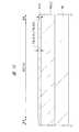
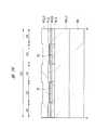
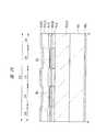
以下、図面を参照しながら本実施の形態の半導体レーザ(半導体装置)について詳細に説明する。図1〜図3は、本実施の形態の半導体レーザの構成を示す断面図であり、図4は、本実施の形態の半導体レーザの構成を示す平面図である。例えば、図1は、図4のA−A部に、図2は、図4のB−B部に、図3は、図4のC−C部に対応する。(Embodiment 1)
Hereinafter, the semiconductor laser (semiconductor device) of the present embodiment will be described in detail with reference to the drawings. 1 to 3 are sectional views showing the configuration of the semiconductor laser according to the present embodiment, and FIG. 4 is a plan view showing the configuration of the semiconductor laser according to the present embodiment. For example, FIG. 1 corresponds to the AA portion of FIG. 4, FIG. 2 corresponds to the BB portion of FIG. 4, and FIG. 3 corresponds to the CC portion of FIG.
[構造説明]
図1に示すように、本実施の形態の半導体レーザは、基板としてn型基板NSを用い、その上に順次積層された、複数の窒化物半導体層を有する。具体的には、n型基板NS上に、n型クラッド層NCLD、n型光ガイド層NLG、活性層MQW、p型光ガイド層PLG、p型クラッド層PCLDおよびp型コンタクト層PCNTが下から順に配置されている。このように、本実施の形態の半導体レーザは、活性層MQWが上層および下層に配置された逆導電型の窒化物半導体により挟まれた構造を有している。[Description of structure]
As shown in FIG. 1, the semiconductor laser according to the present embodiment uses an n-type substrate NS as a substrate and has a plurality of nitride semiconductor layers sequentially stacked thereon. Specifically, an n-type cladding layer NCLD, an n-type light guide layer NLG, an active layer MQW, a p-type light guide layer PLG, a p-type cladding layer PCLD, and a p-type contact layer PCNT are formed on the n-type substrate NS from below. Arranged in order. As described above, the semiconductor laser of the present embodiment has a structure in which the active layer MQW is sandwiched between the reverse conductivity type nitride semiconductors arranged in the upper layer and the lower layer.
そして、最上層のp型コンタクト層PCNT上には、p側電極PELが配置され、n型基板NSの裏面には、n側電極NELが配置されている。p型コンタクト層PCNTとp側電極PELとは、絶縁層(絶縁膜)ILの開口部OAを介して接している。 A p-side electrode PEL is disposed on the uppermost p-type contact layer PCNT, and an n-side electrode NEL is disposed on the back surface of the n-type substrate NS. The p-type contact layer PCNT and the p-side electrode PEL are in contact with each other through the opening OA of the insulating layer (insulating film) IL.
ここで、本実施の形態の半導体レーザにおいては、n型クラッド層NCLDとn型光ガイド層NLGとの間に、電流ブロック層(電流ブロック膜、電流ブロック領域)BLが配置されている。この電流ブロック層BLは、領域1Aの両側に配置され、電流ブロック層BL間、即ち、領域1Aが電流狭窄領域となる。 Here, in the semiconductor laser of the present embodiment, a current block layer (current block film, current block region) BL is disposed between the n-type cladding layer NCLD and the n-type light guide layer NLG. The current block layers BL are disposed on both sides of the
以下に半導体レーザの動作について簡単に説明する。 The operation of the semiconductor laser will be briefly described below.
まず、p側電極PELに正電圧を印加し、n側電極NELに負電圧を印加する。これにより、p側電極PELからn側電極NELに向かって順方向電流が流れ、p側電極PELからp型コンタクト層PCNT、p型クラッド層PCLDおよびp型光ガイド層PLGを介して活性層MQWに正孔が注入される。一方、n側電極NELからは、n型基板NSに電子が注入され、注入された電子は、n型クラッド層NCLDおよびn型光ガイド層NLGを介して、活性層MQWに注入される。そして、電流ブロック層BLによりp側電極PELからn側電極NELに向かって流れる順方向電流の領域が制約され、電流ブロック層BL間、即ち、領域1Aが電流狭窄領域となる。 First, a positive voltage is applied to the p-side electrode PEL, and a negative voltage is applied to the n-side electrode NEL. As a result, a forward current flows from the p-side electrode PEL toward the n-side electrode NEL, and the active layer MQW passes from the p-side electrode PEL through the p-type contact layer PCNT, the p-type cladding layer PCLD, and the p-type light guide layer PLG. Holes are injected into the. On the other hand, electrons are injected from the n-side electrode NEL into the n-type substrate NS, and the injected electrons are injected into the active layer MQW via the n-type cladding layer NCLD and the n-type light guide layer NLG. The region of forward current flowing from the p-side electrode PEL to the n-side electrode NEL is restricted by the current block layer BL, and the region between the current block layers BL, that is, the
活性層MQWでは、注入された正孔と電子によって反転分布が形成され、電子が伝導帯から価電子帯に誘導放出によって遷移することにより、位相の揃った光が発生する。そして、活性層MQWで発生した光は、活性層MQWよりも屈折率の低い周囲の半導体層(p型クラッド層PCLDおよびn型クラッド層NCLD)により、活性層MQW内に閉じ込められる。さらに、活性層MQW内に閉じ込められている光は、半導体レーザに形成されている劈開面(端面、レーザ端面、光出射端面)CPからなる共振器を往復することにより、誘導放出によって増幅される。その後、活性層MQW内でレーザ光Lが発振して、レーザ光Lが射出される。このとき、電流ブロック層BL間(領域1A、電流狭窄領域)に対応する窓領域WAの活性層MQWからレーザ光Lが射出される(図4参照)。 In the active layer MQW, an inversion distribution is formed by the injected holes and electrons, and the electrons transition from the conduction band to the valence band by stimulated emission, whereby light having a uniform phase is generated. The light generated in the active layer MQW is confined in the active layer MQW by the surrounding semiconductor layers (p-type cladding layer PCLD and n-type cladding layer NCLD) having a refractive index lower than that of the active layer MQW. Further, the light confined in the active layer MQW is amplified by stimulated emission by reciprocating a resonator formed of a cleavage plane (end face, laser end face, light emitting end face) CP formed in the semiconductor laser. . Thereafter, the laser beam L oscillates in the active layer MQW, and the laser beam L is emitted. At this time, the laser beam L is emitted from the active layer MQW in the window area WA corresponding to the area between the current block layers BL (
ここで、本実施の形態においては、追って詳細に説明するように、電流ブロック層BLが、光出射端面である劈開面CPから後退して配置されている。別の言い方をすれば、劈開面CPから電流ブロック層BLまでの領域である窓領域WAには、電流ブロック層BLが形成されていない(図12参照)。そして、光出射端面である劈開面CPの近傍に配置される窓領域WAの活性層MQWの層厚TMQWWは、電流ブロック層BL間(領域1A、電流狭窄領域)に形成される活性層MQWの層厚TMQW1Aより小さい(TMQWW<TMQW1A、図3参照)。 Here, in the present embodiment, as will be described in detail later, the current blocking layer BL is disposed so as to recede from the cleavage plane CP that is the light emitting end face. In other words, the current block layer BL is not formed in the window region WA that is a region from the cleavage plane CP to the current block layer BL (see FIG. 12). The layer thickness TMQWW of the active layer MQW in the window region WA disposed in the vicinity of the cleavage plane CP that is the light emitting end surface is equal to that of the active layer MQW formed between the current block layers BL (
このように、窓領域WAの活性層MQWを電流狭窄領域の活性層MQWより薄くすることで、量子効果により、窓領域WAにおける活性層MQWのバンドギャップが大きくなる。このため、光出射端面の光学損傷(Catastrophic Optical Damage:COD)による端面破壊を抑制することができる。詳細は、後述する。 Thus, by making the active layer MQW in the window region WA thinner than the active layer MQW in the current confinement region, the band gap of the active layer MQW in the window region WA is increased due to the quantum effect. For this reason, end face destruction due to optical damage (Catastrophic Optical Damage: COD) of the light exit end face can be suppressed. Details will be described later.
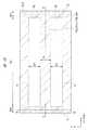
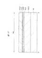
以下に、図1〜図4を参照しながら本実施の形態の半導体レーザの構成を詳細に説明する。図4の平面図に示すように、本実施の形態の半導体レーザは、例えば、X方向に長辺を有する矩形の外形(チップ領域)を有する。そして、本実施の形態の半導体レーザは、窓領域WAと活性領域ACとを有する。 Hereinafter, the configuration of the semiconductor laser according to the present embodiment will be described in detail with reference to FIGS. As shown in the plan view of FIG. 4, the semiconductor laser of the present embodiment has, for example, a rectangular outer shape (chip region) having long sides in the X direction. The semiconductor laser according to the present embodiment has a window area WA and an active area AC.
窓領域WAは、Y方向に延在する矩形(四角形)状の領域であり、矩形の外形(チップ領域)の両側に配置されている。この窓領域WAは、劈開面CPから電流ブロック層BLの端部までの領域である。 The window area WA is a rectangular (quadrangle) -shaped area extending in the Y direction, and is arranged on both sides of a rectangular outer shape (chip area). This window area WA is an area from the cleavage plane CP to the end of the current blocking layer BL.
活性領域ACは、窓領域WA間に位置する。そして、この活性領域ACには、2つの電流ブロック層BLが配置されている。電流ブロック層BLは、X方向に長辺を有する矩形状である。2つの電流ブロック層BL間は、電流狭窄領域となる。この電流狭窄領域は、X方向に長辺を有する矩形状である。ここでは、図4に示すように、活性領域ACにおいて、電流狭窄領域に対応する略中央部を領域1Aとし、領域1Aの両側の領域のうち、電流ブロック層BLが配置される領域を領域2Aとし、領域2Aのさらに外側の領域を領域3Aとして示してある。 The active area AC is located between the window areas WA. In the active region AC, two current block layers BL are arranged. The current block layer BL has a rectangular shape having long sides in the X direction. A current confinement region is formed between the two current block layers BL. This current confinement region has a rectangular shape having a long side in the X direction. Here, as shown in FIG. 4, in the active region AC, the substantially central portion corresponding to the current confinement region is defined as a
図1は、図4に示す平面図のA−A断面部に対応する。また、図2は、図4に示す平面図のB−B断面部に、図3は、図4に示す平面図のC−C断面部に対応する。 FIG. 1 corresponds to the AA cross section of the plan view shown in FIG. 2 corresponds to the BB cross section of the plan view shown in FIG. 4, and FIG. 3 corresponds to the CC cross section of the plan view shown in FIG.
前述したように、n型基板NS上には、n型クラッド層NCLDが配置されている。 As described above, the n-type cladding layer NCLD is disposed on the n-type substrate NS.
n型基板NSとしては、例えば、n型不純物が導入された窒化ガリウム(GaN)からなる基板(n型GaN基板)を用いる。そして、このn型基板NSは、<1-100>方向に傾斜した(0001)面を主面とする。別の言い方をすれば、n型基板NSは、(0001)面から<1-100>方向に傾斜している。言い換えれば、n型基板NSは、(0001)面から<1-100>方向にオフ角を有する。傾斜の角度(オフ角θ)は、例えば、0.1°〜3°の範囲であり、好ましくは、0.2°〜1°の範囲である。 As the n-type substrate NS, for example, a substrate (n-type GaN substrate) made of gallium nitride (GaN) into which an n-type impurity is introduced is used. The n-type substrate NS has a (0001) plane inclined in the <1-100> direction as a main surface. In other words, the n-type substrate NS is inclined in the <1-100> direction from the (0001) plane. In other words, the n-type substrate NS has an off angle in the <1-100> direction from the (0001) plane. The inclination angle (off angle θ) is, for example, in the range of 0.1 ° to 3 °, and preferably in the range of 0.2 ° to 1 °.
図5(a)は、GaNの結晶構造を示す図であり、(b)は、オフ角を示す図である。例えば、図5(a)に示す六角柱の上面が(0001)面であり、<1-100>方向を矢印で示す。この<1-100>方向に対し、上記オフ角θで傾斜する面が主面となる(図5(b))。 FIG. 5A is a diagram showing a crystal structure of GaN, and FIG. 5B is a diagram showing an off angle. For example, the upper surface of the hexagonal column shown in FIG. 5A is the (0001) plane, and the <1-100> direction is indicated by an arrow. With respect to this <1-100> direction, the surface inclined at the off-angle θ is the main surface (FIG. 5B).
このように、(0001)面から<1-100>方向に傾斜したn型基板NS上に、結晶成長により形成された層は、(0001)面から<1-100>方向に傾斜する。このように、n型基板NS上の層にもオフ角が引き継がれる。 As described above, the layer formed by crystal growth on the n-type substrate NS inclined in the <1-100> direction from the (0001) plane is inclined in the <1-100> direction from the (0001) plane. In this way, the off-angle is also inherited by the layer on the n-type substrate NS.
n型クラッド層NCLDとしては、例えば、n型不純物が導入された窒化アルミニウム・ガリウム層(n型AlGaN層)を用いる。n型クラッド層(n型AlGaN層)NCLDの厚さは、例えば、2μm程度である。このn型クラッド層NCLDは、例えば、n型基板NS上に結晶成長により形成され、n型クラッド層NCLDは、(0001)面から<1-100>方向にオフ角を有する。 As the n-type cladding layer NCLD, for example, an aluminum nitride / gallium layer (n-type AlGaN layer) into which an n-type impurity is introduced is used. The thickness of the n-type cladding layer (n-type AlGaN layer) NCLD is, for example, about 2 μm. The n-type cladding layer NCLD is formed by, for example, crystal growth on the n-type substrate NS, and the n-type cladding layer NCLD has an off angle in the <1-100> direction from the (0001) plane.
また、n型クラッド層NCLD上には、電流ブロック層BLが部分的に配置されている。 Further, the current blocking layer BL is partially disposed on the n-type cladding layer NCLD.
電流ブロック層BLとしては、窒化アルミニウム層(AlN層)を用いる。なお、電流ブロック層BLとして、窒化アルミニウム・ガリウム層(AlGaN層)を用いてもよい。電流ブロック層(AlN層)BLの厚さは、例えば、0.1μm程度である。前述したように、電流ブロック層BLは、X方向に長辺を有する矩形状であり、領域1Aの両側に配置される(図4参照)。この電流ブロック層BLは、例えば、n型クラッド層NCLD上に比較的低温(例えば、n型クラッド層NCLDの成長温度より低い温度)で成長させる。このような形成方法により、アモルファス状の電流ブロック層BLを形成することができ、電流ブロック層BLの加工(エッチング)が容易となる。 As the current blocking layer BL, an aluminum nitride layer (AlN layer) is used. Note that an aluminum nitride / gallium layer (AlGaN layer) may be used as the current blocking layer BL. The thickness of the current block layer (AlN layer) BL is, for example, about 0.1 μm. As described above, the current blocking layer BL has a rectangular shape having a long side in the X direction, and is disposed on both sides of the
前述したとおり、電流ブロック層BLは、X方向に長辺を有する矩形状である。2つの電流ブロック層BL間は、電流狭窄領域となる。この電流狭窄領域は、X方向に長辺を有する矩形状である。言い換えれば、活性領域ACの中央部の領域1A(電流狭窄領域)の両側の領域2Aに電流ブロック層BLが配置される。この際、電流ブロック層BLは、劈開面CPから後退して配置される(図4、図12参照)。 As described above, the current blocking layer BL has a rectangular shape having long sides in the X direction. A current confinement region is formed between the two current block layers BL. This current confinement region has a rectangular shape having a long side in the X direction. In other words, the current block layer BL is arranged in the
また、n型クラッド層NCLDおよび電流ブロック層BL上には、n型光ガイド層NLGが配置されている。 An n-type light guide layer NLG is disposed on the n-type cladding layer NCLD and the current blocking layer BL.
n型光ガイド層NLGとしては、n型不純物が導入された窒化ガリウム層(n型GaN層)を用いる。n型光ガイド層NLGは、複数の層厚部を有する。n型光ガイド層NLGの窓領域WAの層厚TNLGWは、活性領域ACの領域1A(電流狭窄領域)の層厚TNLG1Aより小さい(TNLGW<TNLG1A)。 As the n-type light guide layer NLG, a gallium nitride layer (n-type GaN layer) into which an n-type impurity is introduced is used. The n-type light guide layer NLG has a plurality of layer thickness portions. The layer thickness TNLGW of the window region WA of the n-type light guide layer NLG is smaller than the layer thickness TNLG1A of the
例えば、結晶成長によりn型光ガイド層NLGを形成した場合、活性領域ACの領域1Aのn型クラッド層NCLD上には、比較的厚い層が形成され、電流ブロック層BL上には、比較的薄い層が形成される。一方、電流ブロック層BLが形成されていない窓領域WAにおいては、上記厚い層と薄い層の間の層厚を有する層が形成される。このように、電流ブロック層BLが形成されていない窓領域WAにおいては、電流ブロック層BLが形成されている活性領域ACの電流ブロック層BL間に比べ、相対的に層厚が薄くなる。また、電流ブロック層BLとして、Alを含有する層を用いた場合には、層表面のAlが酸化し易く、その上部には層が成長し難い。即ち、電流ブロック層BL上には、選択成長効果によりn型ガイド層NLGが形成されない、または、形成されても薄い層となり、電流ブロック層BL間の領域1Aのn型クラッド層NCLD上には比較的厚い層が形成される。一方、電流ブロック層BLが形成されていない窓領域WAにおいては、形成される層の厚いまたは薄いの差がないため、これらの層厚の間の層厚を有する層が形成される。このため、上記のように、TNLGW<TNLG1Aの関係が生じる(図3参照)。n型光ガイド層(n型GaN層)NLGの領域1A(電流狭窄領域)の層厚TNLG1Aは、例えば、0.1μm程度である。 For example, when the n-type light guide layer NLG is formed by crystal growth, a relatively thick layer is formed on the n-type cladding layer NCLD in the
なお、上記n型基板NS、n型クラッド層NCLDおよびn型光ガイド層NLGのn型不純物としては、例えば、シリコン(Si)を用いる。また、n型光ガイド層NLGをアンドープの層としてもよい。 For example, silicon (Si) is used as the n-type impurity of the n-type substrate NS, the n-type cladding layer NCLD, and the n-type light guide layer NLG. The n-type light guide layer NLG may be an undoped layer.
また、n型光ガイド層NLG上には、活性層MQWが配置されている。 An active layer MQW is disposed on the n-type light guide layer NLG.
活性層MQWは、例えば、窒化インジウム・ガリウム層(InGaN層)からなる量子井戸層と、窒化インジウム・ガリウム層(InGaN層)からなる障壁層とを交互に積層した積層体よりなる。このような積層体の構造を、多重量子井戸構造と言う。そして、量子井戸層を構成する窒化インジウム・ガリウム層(InGaN井戸層)のインジウム組成と、障壁層を構成する窒化インジウム・ガリウム層(InGaN障壁層)のインジウム組成とは異なっている。所望の発振波長に応じて、これらの層のインジウム組成比と層厚を調整する。 The active layer MQW is made of, for example, a stacked body in which quantum well layers made of indium gallium nitride layers (InGaN layers) and barrier layers made of indium gallium nitride layers (InGaN layers) are alternately stacked. Such a stacked structure is called a multiple quantum well structure. The indium composition of the indium gallium nitride layer (InGaN well layer) constituting the quantum well layer is different from the indium composition of the indium gallium nitride layer (InGaN barrier layer) constituting the barrier layer. The indium composition ratio and the layer thickness of these layers are adjusted according to the desired oscillation wavelength.
また、活性層MQWは、複数の層厚部を有する。活性層MQWの窓領域WAの層厚TMQWWは、活性領域ACの領域1A(電流狭窄領域)の層厚TMQW1Aより小さい(TMQWW<TMQW1A、図3参照)。 The active layer MQW has a plurality of layer thickness portions. The layer thickness TMQWW of the window region WA of the active layer MQW is smaller than the layer thickness TMQW1A of the
例えば、結晶成長により活性層MQWを形成した場合、活性領域ACの領域1Aのn型光ガイド層NLG上には、比較的厚い層が形成され、電流ブロック層BLの上方には、比較的薄い層が形成される。一方、電流ブロック層BLが形成されていない窓領域WAにおいては、上記厚い層と薄い層の間の層厚を有する層が形成される。このように、活性層MQWにおいても、n型クラッド層NCLDと同様に、電流ブロック層BLが形成されていない窓領域WAにおいては、電流ブロック層BLが形成されている活性領域ACの電流ブロック層BL間に比べ、相対的に層厚が薄くなる。また、前述したとおり、選択成長効果により電流ブロック層BL上には、n型クラッド層NCLDが形成されない、または、形成されても薄い層となっている。このため、電流ブロック層BLの上方には、活性層MQWが形成されない、または、形成されても薄い層となる。一方、電流ブロック層BLが形成されていない窓領域WAにおいては、形成される層の厚いまたは薄いの差がないため、これらの層厚の間の層厚を有する層が形成される。よって、上記のように、TMQWW<TMQW1Aの関係が生じる(図3参照)。活性層MQWを構成する窒化インジウム・ガリウム量子井戸層は、例えば、アンドープのIn0.1Ga0.9N層であり、3nmから10nm程度の層厚で、2層または3層程度から構成される。障壁層を構成する窒化インジウム・ガリウム層は、アンドープのIn0.01Ga0.99N層であり、10nmから20nm程度の層厚を有する。For example, when the active layer MQW is formed by crystal growth, a relatively thick layer is formed on the n-type light guide layer NLG in the
また、活性層MQW上には、p型光ガイド層PLGが配置されている。 A p-type light guide layer PLG is disposed on the active layer MQW.
p型光ガイド層PLGとしては、p型不純物が導入された窒化ガリウム層(p型GaN層)を用いる。このp型光ガイド層PLGも、n型光ガイド層NLGや活性層MQWと同様に、複数の層厚部を有していてもよい。例えば、p型光ガイド層PLGの窓領域WAの層厚TPLGWは、活性領域ACの領域1A(電流狭窄領域)の層厚TPLG1Aより小さい(TPLGW<TPLG1A、図3参照)。 As the p-type light guide layer PLG, a gallium nitride layer (p-type GaN layer) into which p-type impurities are introduced is used. This p-type light guide layer PLG may also have a plurality of layer thickness portions, like the n-type light guide layer NLG and the active layer MQW. For example, the layer thickness TPLGW of the window region WA of the p-type light guide layer PLG is smaller than the layer thickness TPLG1A of the
例えば、結晶成長によりp型光ガイド層PLGを形成した場合、活性領域ACの領域1Aの活性層MQW上には、比較的厚い層が形成され、電流ブロック層BLの上方には、比較的薄い層が形成される。一方、電流ブロック層BLが形成されていない窓領域WAにおいては、上記厚い層と薄い層の間の層厚を有する層が形成される。このように、p型光ガイド層PLGにおいても、n型ガイド層NLGや活性層MQWと同様に、電流ブロック層BLが形成されていない窓領域WAにおいては、電流ブロック層BLが形成されている活性領域ACの電流ブロック層BL間に比べ、相対的に層厚が薄くなる。また、前述したとおり、電流ブロック層BL上には、活性層MQWが形成されない、または、形成されても薄い層となっている。このため、電流ブロック層BLの上方には、p型光ガイド層PLGが形成されない、または、形成されても薄い層となる。一方、電流ブロック層BLが形成されていない窓領域WAにおいては、形成される層の厚いまたは薄いの差がないため、これらの層厚の間の層厚を有する層が形成される。よって、上記のように、TPLGW<TPLG1Aの関係が生じる(図3参照)。p型光ガイド層PLGの領域1A(電流狭窄領域)の層厚TPLG1Aは、例えば、0.1μm程度である。 For example, when the p-type light guide layer PLG is formed by crystal growth, a relatively thick layer is formed on the active layer MQW in the
また、p型光ガイド層PLG上には、p型クラッド層PCLDが配置されている。 A p-type cladding layer PCLD is disposed on the p-type light guide layer PLG.
p型クラッド層PCLDとしては、例えば、p型不純物が導入された窒化アルミニウム・ガリウム層(p型AlGaN層)とp型不純物が導入された窒化ガリウム層(p型GaN層)とを交互に積層した超格子層を用いる。p型クラッド層PCLDの厚さは、例えば、0.5μm程度である。なお、p型クラッド層PCLDにおいても、下層の層と同様に、領域によって層厚差が生じていてもよい。但し、p型クラッド層PCLDの層厚は、下層の層(p型光ガイド層PLG、活性層MQWおよびn型光ガイド層NLG)の層厚(例えば、0.3μm以下)より大きく、層厚差が緩和される。 As the p-type cladding layer PCLD, for example, an aluminum nitride / gallium layer (p-type AlGaN layer) into which p-type impurities are introduced and a gallium nitride layer (p-type GaN layer) into which p-type impurities are introduced are alternately laminated. Using the superlattice layer. The thickness of the p-type cladding layer PCLD is, for example, about 0.5 μm. In the p-type cladding layer PCLD, the layer thickness may vary depending on the region, as in the lower layer. However, the layer thickness of the p-type cladding layer PCLD is larger than the layer thickness (for example, 0.3 μm or less) of the lower layer (p-type light guide layer PLG, active layer MQW and n-type light guide layer NLG). The difference is eased.
p型コンタクト層PCNTとしては、p型不純物が導入された窒化ガリウム層(p型GaN層)を用いる。p型GaN層の厚さは、例えば、0.02μm程度である。 As the p-type contact layer PCNT, a gallium nitride layer (p-type GaN layer) into which p-type impurities are introduced is used. The thickness of the p-type GaN layer is, for example, about 0.02 μm.
上記p型光ガイド層PLG、p型クラッド層PCLDおよびp型コンタクト層PCNTのp型不純物としては、例えば、マグネシウム(Mg)を用いる。また、p型光ガイド層PLGをアンドープの層としてもよい。 For example, magnesium (Mg) is used as the p-type impurity of the p-type light guide layer PLG, the p-type cladding layer PCLD, and the p-type contact layer PCNT. The p-type light guide layer PLG may be an undoped layer.
なお、活性層MQWとp型光ガイド層PLGとの間にキャリア閉じ込め層として、p型不純物が導入された窒化アルミニウム・ガリウム層(p型AlGaN層)を設けてもよい。 An aluminum nitride / gallium layer (p-type AlGaN layer) into which a p-type impurity is introduced may be provided as a carrier confinement layer between the active layer MQW and the p-type light guide layer PLG.
ここで、活性層MQWは、n型クラッド層NCLDよりバンドギャップが小さい。また、活性層MQWは、p型クラッド層PCLDよりバンドギャップが小さい。より具体的には、ここでは、活性層MQWの上には、p型の窒化物半導体の積層部が設けられ、活性層MQWは、p型の窒化物半導体の積層部を構成する各層よりバンドギャップが小さい。また、活性層MQWの下には、n型の窒化物半導体の積層部が設けられ、活性層MQWは、n型の窒化物半導体の積層部を構成する各層よりバンドギャップが小さい。また、n型の窒化物半導体の積層部およびp型の窒化物半導体の積層部は、活性層MQWよりも屈折率が低い。 Here, the active layer MQW has a smaller band gap than the n-type cladding layer NCLD. The active layer MQW has a smaller band gap than the p-type cladding layer PCLD. More specifically, here, a p-type nitride semiconductor laminated portion is provided on the active layer MQW, and the active layer MQW has a band higher than each layer constituting the p-type nitride semiconductor laminated portion. The gap is small. In addition, an n-type nitride semiconductor stacked portion is provided under the active layer MQW, and the active layer MQW has a smaller band gap than each layer constituting the n-type nitride semiconductor stacked portion. The n-type nitride semiconductor stacked portion and the p-type nitride semiconductor stacked portion have a refractive index lower than that of the active layer MQW.
そして、電流ブロック層BLは、Alを含有する窒化物半導体よりなり、活性層MQW、n型クラッド層NCLDおよびp型クラッド層PCLDのいずれよりもバンドギャップが大きい。より具体的には、電流ブロック層BLは、活性層MQW、その上のp型の窒化物半導体の積層部およびその下のn型の窒化物半導体の積層部のいずれの層よりもバンドギャップが大きい。 The current blocking layer BL is made of a nitride semiconductor containing Al, and has a larger band gap than any of the active layer MQW, the n-type cladding layer NCLD, and the p-type cladding layer PCLD. More specifically, the current blocking layer BL has a band gap that is higher than any of the active layer MQW, the p-type nitride semiconductor stacked portion thereon, and the n-type nitride semiconductor stacked portion below the active layer MQW. large.
電流狭窄領域(電流ブロック層BL間、領域1A)の幅は、例えば、1μm程度である。この幅(図4のY方向の幅)は、例えば、1μm〜20μmの範囲で調整することができる。また、電流ブロック層BLの幅(図4のY方向の幅)に制限はないが、小さすぎると選択成長効果による層厚差が小さくなるため、例えば、電流狭窄領域の幅と同程度、または電流狭窄領域より広い範囲(例えば、1μm〜50μmの範囲、好ましくは5μm〜30μmの範囲)で調整することが好ましい。 The width of the current confinement region (between the current block layers BL, the
また、窓領域WAのX方向の幅、言い換えれば、劈開面CPからの電流ブロック層BLの後退量は、例えば、2μm〜50μmの範囲、より好ましくは5μm〜20μmの範囲で調整することができる。 Further, the width in the X direction of the window area WA, in other words, the retraction amount of the current blocking layer BL from the cleavage plane CP can be adjusted, for example, in the range of 2 μm to 50 μm, more preferably in the range of 5 μm to 20 μm. .
また、半導体レーザの矩形の外形(チップ領域、図4参照)は、例えば、長辺が600μm〜1000μm、短辺が150μm〜200μmである。 The rectangular outer shape of the semiconductor laser (chip region, see FIG. 4) has, for example, a long side of 600 μm to 1000 μm and a short side of 150 μm to 200 μm.
図4に示すX方向は、光出射方向であり、<1−100>方向となる。よって、電流狭窄領域(領域1A)および電流ブロック層BLは、<1−100>方向に延在している。 The X direction shown in FIG. 4 is the light emission direction and is the <1-100> direction. Therefore, the current confinement region (
p型コンタクト層PCNT上には、絶縁層ILが配置されている。この絶縁層ILとしては、例えば、酸化シリコン膜を用いる。絶縁層ILは、電流狭窄領域(領域1A)上に開口部OAを有する。 An insulating layer IL is disposed on the p-type contact layer PCNT. For example, a silicon oxide film is used as the insulating layer IL. The insulating layer IL has an opening OA on the current confinement region (
p型コンタクト層PCNTとp側電極PELとは、絶縁層(絶縁膜)ILの開口部OAを介して接している。 The p-type contact layer PCNT and the p-side electrode PEL are in contact with each other through the opening OA of the insulating layer (insulating film) IL.
このように、本実施の形態の半導体レーザによれば、2つの電流ブロック層BLを設けることにより、これらの間(領域1A)が電流狭窄領域となる。また、この電流ブロック層BLにより横方向の光を閉じ込めることができる。 As described above, according to the semiconductor laser of the present embodiment, by providing the two current block layers BL, a region between these (
そして、電流狭窄領域(領域1A)の活性層MQWより窓領域WAの活性層MQWを薄く形成することで、窓領域WAにおける活性層MQWのバンドギャップを大きくすることができる。これにより、光出射端面の光学損傷による端面破壊を抑制することができる。 The band gap of the active layer MQW in the window region WA can be increased by forming the active layer MQW in the window region WA thinner than the active layer MQW in the current confinement region (
即ち、半導体レーザの光出射端面付近においては、光の吸収に伴い温度が上昇し得る。温度が上昇すると光出射端面付近の半導体層のバンドギャップが小さくなり、レーザ光の吸収が増大する。このように、光の吸収→温度上昇→さらなる光の吸収→さらなる温度上昇という悪循環が起こると、最終的には光出射端面の光学損傷によって端面破壊が発生し、レーザ発振が不可能となる。 That is, in the vicinity of the light emitting end face of the semiconductor laser, the temperature can rise as light is absorbed. When the temperature rises, the band gap of the semiconductor layer in the vicinity of the light emitting end face decreases, and the absorption of the laser light increases. As described above, when a vicious cycle of light absorption → temperature rise → further light absorption → further temperature rise occurs, end face destruction occurs due to optical damage of the light emitting end face, and laser oscillation becomes impossible.
これに対し、本実施の形態においては、電流狭窄領域(領域1A)の活性層MQWより窓領域WAの活性層MQWを薄く形成することで(TMQWW<TMQW1A)、窓領域WAにおける活性層MQWのバンドギャップを大きくすることができる。よって、光出射端面付近における光の吸収を抑制することができ、光出射端面の光学損傷を抑制することができる。 On the other hand, in the present embodiment, the active layer MQW in the window region WA is formed thinner than the active layer MQW in the current confinement region (
また、(0001)面から<1-100>方向に傾斜したオフ角を有する基板を用いることで、電流ブロック層BL上と電流狭窄領域(領域1A)の層厚差を大きくすることができ、電流ブロック層BLの有無により、電流狭窄領域(領域1A)の活性層MQWより窓領域WAの活性層MQWを薄く形成することができる。このように、オフ角を有する基板および電流ブロック層BLにより、窓領域WAの活性層MQWを電流狭窄領域(領域1A)の活性層MQWより薄く形成することができる。 Moreover, by using a substrate having an off angle inclined in the <1-100> direction from the (0001) plane, the layer thickness difference between the current blocking layer BL and the current confinement region (
また、2つの電流ブロック層BL間(領域1A)を電流狭窄領域とすることで、この電流ブロック層BLにより横方向の光を閉じ込めることができ、リッジ構造とする必要が無く、リッジ構造を形成する工程(p型コンタクト層PCNTおよびp型クラッド層PCLDのパターニング工程)が不要となる。また、p型クラッド層PCLDが広い領域に形成されるため、横方向への放熱性が良好となる。また、p型コンタクト層PCNTとp側電極PELとの接続領域を大きく確保することができ、これらの接続抵抗を低減することができる。そして、これにより、半導体レーザの動作電圧を低減することができる。 Further, by making the current confinement region between the two current block layers BL (
[製法説明]
次いで、図6〜図32を参照しながら、本実施の形態の半導体レーザの製造方法を説明するとともに、当該半導体レーザの構成をより明確にする。図6〜図32(図17を除く)は、本実施の形態の半導体レーザの製造工程を示す断面図または平面図である。[Product description]
Next, the method for manufacturing the semiconductor laser according to the present embodiment will be described with reference to FIGS. 6 to 32, and the configuration of the semiconductor laser will be clarified. 6 to 32 (excluding FIG. 17) are cross-sectional views or plan views showing the manufacturing steps of the semiconductor laser of the present embodiment.
図6に示すように、n型基板NSとして、例えばn型不純物が導入された窒化ガリウム(GaN)からなり、(0001)面から<1-100>方向にオフ角を有する基板を準備する(図5参照)。オフ角θは、例えば、0.1°〜3°程度であり、好ましくは、0.2°〜1°程度である。なお、このn型基板NSとしては、フリースタンディング基板を用いることができる。フリースタンディング基板とは、炭化珪素基板やサファイア基板などの支持基板上に窒化ガリウムを成長させ、その後、支持基板上を除去して窒化ガリウム単独とした基板である。 As shown in FIG. 6, as the n-type substrate NS, for example, a substrate made of gallium nitride (GaN) into which an n-type impurity is introduced and having an off angle in the <1-100> direction from the (0001) plane is prepared ( (See FIG. 5). The off angle θ is, for example, about 0.1 ° to 3 °, and preferably about 0.2 ° to 1 °. As this n-type substrate NS, a free standing substrate can be used. A free-standing substrate is a substrate in which gallium nitride is grown on a support substrate such as a silicon carbide substrate or a sapphire substrate, and then the support substrate is removed to make gallium nitride alone.
次いで、図7に示すように、上記n型基板NS上に、n型クラッド層NCLDとして、n型AlGaN層を形成する。例えば、MOVPE(Metal Organic Vapor Phase Epitaxy、有機金属気相成長)装置を用い、キャリアガスと原料ガスを、装置内に導入しながら、n型クラッド層NCLD(n型AlGaN層)を結晶成長させる。キャリアガスには、水素、または窒素、または水素と窒素の混合ガスを用いる。原料ガスには、窒化物半導体の構成元素を含むガスを用いる。例えば、n型クラッド層NCLD(n型AlGaN層)の成膜の際には、Al、Ga、N原料として、TMAl(トリメチルアルミニウム)、TMGa(トリメチルガリウム)、NH3(アンモニア)をそれぞれ用い、n型不純物の原料として、SiH4(シラン)を用いる。n型基板NSを上記装置にセットし、NH3を供給しながら基板を昇温し、成長温度に到達後、原料ガスをキャリアガスとともに装置内に導入しながら、2μm程度の厚さのn型クラッド層NCLD(n型AlGaN層)を結晶成長させる。成長温度は、例えば、1000℃〜1100℃程度である。Next, as shown in FIG. 7, an n-type AlGaN layer is formed as an n-type cladding layer NCLD on the n-type substrate NS. For example, using an MOVPE (Metal Organic Vapor Phase Epitaxy) apparatus, an n-type cladding layer NCLD (n-type AlGaN layer) is crystal-grown while introducing a carrier gas and a source gas into the apparatus. As the carrier gas, hydrogen, nitrogen, or a mixed gas of hydrogen and nitrogen is used. As the source gas, a gas containing a constituent element of a nitride semiconductor is used. For example, when forming an n-type cladding layer NCLD (n-type AlGaN layer), TMAl (trimethylaluminum), TMGa (trimethylgallium), and NH3 (ammonia) are used as Al, Ga, and N raw materials, SiH4 (silane) is used as a raw material for the n-type impurity. The n-type substrate NS is set in the above apparatus, the temperature of the substrate is raised while supplying NH3, and after reaching the growth temperature, the n-type having a thickness of about 2 μm is introduced while introducing the source gas into the apparatus together with the carrier gas. The cladding layer NCLD (n-type AlGaN layer) is crystal-grown. The growth temperature is, for example, about 1000 ° C. to 1100 ° C.
次いで、図8に示すように、装置内の温度を低下させ、n型クラッド層NCLDの成長温度より低い温度で、0.1μm程度の厚さの電流ブロック層BL(AlN層)を成長させる。電流ブロック層BL(AlN層)の成膜の際には、Al、N原料として、TMAl(トリメチルアルミニウム)、NH3(アンモニア)をそれぞれ用いる。成長温度は、例えば、200℃〜600℃程度である。このように、比較的低温(例えば、n型クラッド層NCLDや後述の活性層MQWより低温)で成膜することにより、アモルファス状態の電流ブロック層BL(AlN層)を形成することができる。Next, as shown in FIG. 8, the temperature in the apparatus is lowered, and a current blocking layer BL (AlN layer) having a thickness of about 0.1 μm is grown at a temperature lower than the growth temperature of the n-type cladding layer NCLD. When forming the current blocking layer BL (AlN layer), TMAl (trimethylaluminum) and NH3 (ammonia) are used as Al and N raw materials, respectively. The growth temperature is, for example, about 200 ° C. to 600 ° C. In this way, the amorphous current blocking layer BL (AlN layer) can be formed by forming the film at a relatively low temperature (for example, a temperature lower than that of the n-type cladding layer NCLD or the active layer MQW described later).
次いで、上記基板をMOVPE装置より取り出し、図9〜図12に示すように、電流ブロック層BL(AlN層)をパターニングする。例えば、電流ブロック層BL(AlN層)上に、ハードマスク(図示せず)を形成する。例えば、CVD(Chemical Vapor Deposition)法などを用いて、電流ブロック層BL(AlN層)上に、酸化シリコン膜を形成する。次いで、酸化シリコン膜上に、フォトレジスト膜を塗布した後、フォトリソグラフィ技術を用いて電流ブロック層BL(AlN層)を残存させる領域にのみフォトレジスト膜を残存させる。次いで、フォトレジスト膜をマスクとして、ハードマスク(酸化シリコン膜)をエッチングする。次いで、フォトレジスト膜をアッシングなどにより除去する。次いで、ハードマスク(酸化シリコン膜)をマスクとして、電流ブロック層BL(AlN層)をエッチングする。エッチング法としては、ドライエッチング法およびウェットエッチング法のいずれを用いてもよい。前述したとおり、電流ブロック層BL(AlN層)を比較的低温で成膜し、アモルファス状態の電流ブロック層BL(AlN層)を形成しておくことにより、ウェットエッチング法を用いた場合でも、容易にエッチングを行うことができる。この後、ハードマスク(酸化シリコン膜)を除去する。なお、アモルファス状態の電流ブロック層BL(AlN層)は、以降の処理の熱負荷により結晶化する。 Next, the substrate is taken out of the MOVPE apparatus, and the current blocking layer BL (AlN layer) is patterned as shown in FIGS. For example, a hard mask (not shown) is formed on the current block layer BL (AlN layer). For example, a silicon oxide film is formed on the current block layer BL (AlN layer) using a CVD (Chemical Vapor Deposition) method or the like. Next, after a photoresist film is applied on the silicon oxide film, the photoresist film is left only in a region where the current block layer BL (AlN layer) is left using a photolithography technique. Next, the hard mask (silicon oxide film) is etched using the photoresist film as a mask. Next, the photoresist film is removed by ashing or the like. Next, the current block layer BL (AlN layer) is etched using the hard mask (silicon oxide film) as a mask. As the etching method, either a dry etching method or a wet etching method may be used. As described above, by forming the current block layer BL (AlN layer) at a relatively low temperature and forming the amorphous current block layer BL (AlN layer), it is easy even when the wet etching method is used. Etching can be performed. Thereafter, the hard mask (silicon oxide film) is removed. Note that the amorphous current blocking layer BL (AlN layer) is crystallized by the heat load of the subsequent processing.
上記エッチングにより、2つの電流ブロック層BLが活性領域ACに形成される。電流ブロック層BLの上面から見た平面形状は、例えば、矩形状(四角形状)である(図12)。そして、電流ブロック層BLは、<1−100>方向に長辺を有する。2つの電流ブロック層BLは、所定の間隔(例えば、1μm〜20μm程度)をおいて形成される。言い換えれば、電流ブロック層BLは、図12に示す領域1Aの両側に形成される。この電流ブロック層BL間(領域1A)は、電流狭窄領域となる。領域1Aは、X方向に長辺を有する矩形状である。 By the etching, two current blocking layers BL are formed in the active region AC. The planar shape seen from the upper surface of the current blocking layer BL is, for example, a rectangular shape (square shape) (FIG. 12). The current blocking layer BL has a long side in the <1-100> direction. The two current block layers BL are formed at a predetermined interval (for example, about 1 μm to 20 μm). In other words, the current blocking layer BL is formed on both sides of the
また、電流ブロック層BLは、チップ領域(半導体レーザ形成領域)の端部まで延在していない。別の言い方をすれば、電流ブロック層BLは、チップ領域(半導体レーザ形成領域のY方向に延在する辺)から後退して配置される。このため、Y方向に延在する辺(劈開面CL、端面)から所定の幅の領域には、電流ブロック層BLが形成されていない。この領域が、窓領域WAとなる。窓領域WAのX方向の幅は、例えば、2μm〜50μm程度、より好ましくは、5μm〜20μm程度である。 The current block layer BL does not extend to the end of the chip region (semiconductor laser formation region). In other words, the current blocking layer BL is disposed so as to recede from the chip region (side extending in the Y direction of the semiconductor laser forming region). For this reason, the current block layer BL is not formed in a region having a predetermined width from the side (cleavage surface CL, end surface) extending in the Y direction. This area is the window area WA. The width in the X direction of the window area WA is, for example, about 2 μm to 50 μm, and more preferably about 5 μm to 20 μm.
次いで、図13〜図16に示すように、電流ブロック層BL(AlN層)およびn型クラッド層NCLD(n型AlGaN層)上に、n型光ガイド層NLGとして、n型GaN層を形成する。例えば、MOVPE装置を用い、キャリアガスと原料ガスを、装置内に導入しながら、n型光ガイド層NLG(n型GaN層)を結晶成長させる。原料ガスとしては、Ga、N原料として、TMGa(トリメチルガリウム)、NH3(アンモニア)をそれぞれ用い、n型不純物の原料として、SiH4(シラン)を用いる。成長温度は、例えば、1000℃〜1100℃程度である。Next, as shown in FIGS. 13 to 16, an n-type GaN layer is formed as an n-type light guide layer NLG on the current block layer BL (AlN layer) and the n-type cladding layer NCLD (n-type AlGaN layer). . For example, the MOVPE apparatus is used to grow an n-type light guide layer NLG (n-type GaN layer) while introducing a carrier gas and a source gas into the apparatus. As source gases, TMGa (trimethylgallium) and NH3 (ammonia) are used as Ga and N sources, respectively, and SiH4 (silane) is used as an n-type impurity source. The growth temperature is, for example, about 1000 ° C. to 1100 ° C.
図17は、電流ブロック層BL間(領域1A)のn型クラッド層上に形成された層の層厚とオフ角度との関係を示した図である。縦軸は、電流ブロック層BL間に形成された層の層厚を示し、横軸は、<1−100>方向の傾斜角度(オフ角度)[deg]を示す。図17に示すように、オフ角度が大きくなるほど選択成長効果が大きく、電流ブロック層BL間(領域1A)に形成される層の厚さが大きくなっている。 FIG. 17 is a diagram showing the relationship between the layer thickness of the layer formed on the n-type cladding layer between the current blocking layers BL (
一方、窓領域WAにおいては、電流ブロック層BLが形成されていないため、電流ブロック層BL間のn型光ガイド層NLGより薄いn型光ガイド層NLGが形成される。また、電流ブロック層BLとして、AlN層のようなAlを含有する層を用いた場合には、層表面のAlが酸化し易く、その上部には層が成長し難いので、電流ブロック層BL上には、n型クラッド層NCLDが形成されない、または、形成されても薄い層となる。よって、n型光ガイド層NLGの層厚において、領域1Aの層厚TNLG1Aおよび窓領域WAの層厚TNLGWについて、TNLG1A>TNLGWの関係が生じることとなる(図13〜図16参照)。より詳しくは、n型光ガイド層NLGの層厚において、領域1Aの層厚TNLG1A、領域2Aの層厚(ここでは、TNLG2Aとする)および窓領域WAの層厚TNLGWについて、TNLG1A>TNLGW>TNLG2Aの関係が生じることとなる。n型光ガイド層NLG(n型GaN層)の層厚は、領域1Aにおいて、例えば、0.1μm程度である。 On the other hand, since the current block layer BL is not formed in the window area WA, an n-type light guide layer NLG thinner than the n-type light guide layer NLG between the current block layers BL is formed. Further, when an Al-containing layer such as an AlN layer is used as the current blocking layer BL, Al on the surface of the layer is easily oxidized, and the layer is difficult to grow on the upper portion thereof. The n-type cladding layer NCLD is not formed, or even if it is formed, it becomes a thin layer. Therefore, in the layer thickness of the n-type light guide layer NLG, the relationship of TNLG1A> TNLGW occurs with respect to the layer thickness TNLG1A of the
次いで、図18〜図21に示すように、原料ガスを切り替え、n型光ガイド層NLG上に活性層MQW(インジウム組成の異なるInGaN井戸層とInGaN障壁層を交互に積層した多重量子井戸構造体)を結晶成長させる。活性層MQW(InGaN井戸層とInGaN障壁層)の成膜の際には、In、Ga、N原料として、TMIn(トリメチルインジウム)、TMGa(トリメチルガリウム)、NH3(アンモニア)をそれぞれ用いる。In原料であるTMIn(トリメチルインジウム)の流量を切り替えることにより、インジウム組成の異なるInGaN井戸層とInGaN障壁層を交互に積層することができる。成長温度は、例えば、800℃〜900℃程度である。Next, as shown in FIG. 18 to FIG. 21, the source gas is switched, and the active layer MQW (multi-quantum well structure in which InGaN well layers and InGaN barrier layers having different indium compositions are alternately stacked on the n-type light guide layer NLG. ) Is grown. When forming the active layer MQW (InGaN well layer and InGaN barrier layer), TMIn (trimethylindium), TMGa (trimethylgallium), and NH3 (ammonia) are used as In, Ga, and N raw materials, respectively. By switching the flow rate of TMIn (trimethylindium) which is an In raw material, InGaN well layers and InGaN barrier layers having different indium compositions can be alternately stacked. The growth temperature is, for example, about 800 ° C. to 900 ° C.
この活性層MQWにおいても、n型光ガイド層NLGと同様に、電流ブロック層BL間(領域1A)に形成される層の厚さが大きくなる。また、窓領域WAにおいては、電流ブロック層BLが形成されていないため、電流ブロック層BL間(領域1A)の活性層MQWより薄い活性層MQWが形成される。また、電流ブロック層BL上またはその上部の薄いn型クラッド層NCLD上には、活性層MQWが形成されない、または、形成されても薄い層となる。よって、活性層MQWの層厚において、領域1Aの層厚TMQW1Aおよび窓領域WAの層厚TMQWWについて、TMQW1A>TMQWWの関係が生じる(図18〜図21参照)。より詳しくは、活性層MQWの層厚において、領域1Aの層厚TMQW1A、領域2Aの層厚(ここでは、TMQW2Aとする)および窓領域WAの層厚TMQWWについて、TMQW1A>TMQWW>TMQW2Aの関係が生じる。 Also in the active layer MQW, the thickness of the layer formed between the current block layers BL (
領域1Aにおいて、活性層MQWを構成するInGaN井戸層の厚さは3nmから10nm程度で、2層または3層程度から構成され、InGaN障壁層の厚さは10nmから20nm程度積層する。 In the
次いで、図22〜図25に示すように、原料ガスを切り替え、活性層MQW上に、p型光ガイド層PLG(p型GaN層)を結晶成長させる。p型光ガイド層PLG(p型GaN層)の成膜の際には、Ga、N原料として、TMGa(トリメチルガリウム)、NH3(アンモニア)をそれぞれ用い、p型不純物の原料として、Cp2Mg(ビスシクロペンタジエニルマグネシウム)を用いる。成長温度は、例えば、1000℃〜1100℃程度である。Next, as shown in FIGS. 22 to 25, the source gas is switched, and a p-type light guide layer PLG (p-type GaN layer) is grown on the active layer MQW. When forming the p-type light guide layer PLG (p-type GaN layer), TMGa (trimethylgallium) and NH3 (ammonia) are used as Ga and N raw materials, respectively, and Cp2 is used as a p-type impurity raw material. Mg (biscyclopentadienyl magnesium) is used. The growth temperature is, for example, about 1000 ° C. to 1100 ° C.
このp型光ガイド層PLG(p型GaN層)においても、活性層MQWやn型光ガイド層NLGと同様に、複数の層厚部が形成されていてもよい。例えば、領域1Aの層厚TPLG1Aおよび窓領域WAの層厚TPLGWについて、TPLG1A>TPLGWの関係が生じていてもよい(図22〜図25参照)。より詳しくは、領域1Aの層厚TPLG1A、領域2Aの層厚(ここでは、TPLG2Aとする)および窓領域WAの層厚TPLGWについて、TPLG1A>TPLGW>TPLG2Aの関係が生じていてもよい。 Also in the p-type light guide layer PLG (p-type GaN layer), a plurality of layer thickness portions may be formed as in the active layer MQW and the n-type light guide layer NLG. For example, the relationship of TPLG1A> TPLGW may occur for the layer thickness TPLG1A of the
なお、本実施の形態においては、電流ブロック層BL間(領域1A)と窓領域WAとにおける活性層MQWの層厚差が重要で有り、活性層MQWより上層の層においては、領域によって層厚差が生じることが必ずしも必要ではなく、層厚差が緩和されていてもよい。領域1Aにおいて、p型光ガイド層PLG(p型GaN層)の層厚は、例えば、0.1μm程度である。 In the present embodiment, the layer thickness difference of the active layer MQW between the current block layers BL (
次いで、図26〜図28に示すように、原料ガスを切り替え、p型光ガイド層PLG上に、p型クラッド層PCLDを結晶成長させる。p型クラッド層PCLDとして、p型光ガイド層PLG(p型GaN層)上に、例えば、p型不純物が導入された窒化アルミニウム・ガリウム層(p型AlGaN層)とp型不純物が導入された窒化ガリウム層(p型GaN層)とを交互に積層した超格子層を形成する。p型AlGaN層の成膜の際には、Al、Ga、N原料として、TMAl(トリメチルアルミニウム)、TMGa(トリメチルガリウム)、NH3(アンモニア)をそれぞれ用い、p型不純物の原料として、Cp2Mg(ビスシクロペンタジエニルマグネシウム)を用いる。p型GaN層の成膜の際には、上記原料ガスのうち、TMAl(トリメチルアルミニウム)の供給を停止する。このように、原料ガスのうち、Al原料であるTMAl(トリメチルアルミニウム)の供給と停止を繰り返すことにより、p型AlGaN層とp型GaN層とを交互に積層した超格子層よりなるp型クラッド層PCLDを形成することができる。成長温度は、例えば、1000℃〜1100℃程度である。なお、このp型クラッド層PCLDにおいても、下層の層と同様に、領域によって層厚差が生じていてもよいが、ここでは、p型クラッド層PCLDの層厚が下層のp型光ガイド層PLG、活性層MQWおよびn型光ガイド層NLGより大きく、層厚差が緩和されている。Next, as shown in FIGS. 26 to 28, the source gas is switched, and the p-type cladding layer PCLD is grown on the p-type light guide layer PLG. As the p-type cladding layer PCLD, for example, an aluminum nitride / gallium layer (p-type AlGaN layer) into which a p-type impurity is introduced and a p-type impurity are introduced on the p-type light guide layer PLG (p-type GaN layer). A superlattice layer in which gallium nitride layers (p-type GaN layers) are alternately stacked is formed. When forming the p-type AlGaN layer, TMAl (trimethylaluminum), TMGa (trimethylgallium), and NH3 (ammonia) are used as the Al, Ga, and N raw materials, respectively, and Cp2 is used as the p-type impurity raw material. Mg (biscyclopentadienyl magnesium) is used. During the formation of the p-type GaN layer, the supply of TMAl (trimethylaluminum) in the source gas is stopped. In this way, p-type cladding comprising a superlattice layer in which p-type AlGaN layers and p-type GaN layers are alternately stacked by repeatedly supplying and stopping TMAl (trimethylaluminum), which is an Al material, in the source gas. A layer PCLD can be formed. The growth temperature is, for example, about 1000 ° C. to 1100 ° C. In this p-type cladding layer PCLD, the layer thickness may vary depending on the region as in the lower layer, but here, the p-type cladding layer PCLD has a lower p-type light guide layer. It is larger than PLG, active layer MQW, and n-type light guide layer NLG, and the layer thickness difference is relaxed.
次いで、図29に示すように、原料ガスを切り替え、p型クラッド層PCLD上にp型コンタクト層PCNT(p型GaN層)を結晶成長させる。p型コンタクト層PCNT(p型GaN層)の成膜の際には、Ga、N原料として、TMGa(トリメチルガリウム)、NH3(アンモニア)をそれぞれ用い、p型不純物の原料として、Cp2Mg(ビスシクロペンタジエニルマグネシウム)を用いる。成長温度は、例えば、1000℃〜1100℃程度である。Next, as shown in FIG. 29, the source gas is switched, and a p-type contact layer PCNT (p-type GaN layer) is grown on the p-type cladding layer PCLD. When forming the p-type contact layer PCNT (p-type GaN layer), TMGa (trimethylgallium) and NH3 (ammonia) are used as Ga and N raw materials, respectively, and Cp2 Mg is used as a p-type impurity raw material. (Biscyclopentadienyl magnesium) is used. The growth temperature is, for example, about 1000 ° C. to 1100 ° C.
次いで、図30および図31に示すように、p型コンタクト層PCNT上に、絶縁層ILとして、例えば、酸化シリコン膜をCVD法などを用いて形成する。次いで、領域1A(電流狭窄領域)上の絶縁層ILを除去する。例えば、領域1A(電流狭窄領域)に開口部を有するフォトレジスト膜(図示せず)をマスクとして、絶縁層ILをエッチングする。次いで、フォトレジスト膜をアッシングなどにより除去する。これにより、領域1A(電流狭窄領域)上の絶縁層ILが除去され、開口部OAが形成される。この開口部OAの底面には、p型コンタクト層PCNTが露出している。 Next, as shown in FIGS. 30 and 31, as the insulating layer IL, for example, a silicon oxide film is formed on the p-type contact layer PCNT using a CVD method or the like. Next, the insulating layer IL on the
次いで、図32に示すように、p型コンタクト層PCNTおよび絶縁層IL上に、p側電極PELを形成する。 Next, as shown in FIG. 32, a p-side electrode PEL is formed on the p-type contact layer PCNT and the insulating layer IL.
次いで、n型基板NSの裏面側を上面とし、n型基板NSの裏面を研磨することにより、n型基板NSを薄膜化する。例えば、n型基板NSを100μm程度の厚さとする。次いで、n型基板NSの裏面に、n側電極NELを形成する(図32)。 Next, the n-type substrate NS is thinned by polishing the back surface of the n-type substrate NS with the back side of the n-type substrate NS as the upper surface. For example, the n-type substrate NS is about 100 μm thick. Next, an n-side electrode NEL is formed on the back surface of the n-type substrate NS (FIG. 32).
この後、複数のチップ領域を有するn型基板NSをチップ領域ごとに切り出す。まず、チップ領域間を劈開する。即ち、あるチップ領域とその隣のチップ領域との間に位置する(窓領域WA)において、線CLに沿って劈開する(図31等参照)。劈開面CPは線CLに対応する。これにより、図4に示す半導体レーザの共振器のミラー面となる劈開面(Y方向に延在する面)CPが形成される。さらに、チップ領域のX方向に延在する辺に沿って切断することにより、チップ片が切り出される。 Thereafter, the n-type substrate NS having a plurality of chip regions is cut out for each chip region. First, the chip area is cleaved. That is, cleavage is performed along the line CL in the window area WA located between a certain chip area and the adjacent chip area (see FIG. 31 and the like). The cleavage plane CP corresponds to the line CL. As a result, a cleavage plane (surface extending in the Y direction) CP, which becomes the mirror surface of the resonator of the semiconductor laser shown in FIG. 4, is formed. Further, the chip piece is cut out by cutting along the side extending in the X direction of the chip region.
以上の工程により、本実施の形態の半導体レーザを形成することができる。 Through the above steps, the semiconductor laser of this embodiment can be formed.
このように、本実施の形態によれば、(0001)面から<1-100>方向にオフ角を有するn型基板NS上に、劈開面CPから後退して電流ブロック層BLを形成し、その上方に活性層MQWを結晶成長することで、劈開面CP近傍の窓領域WAの活性層MQWを電流狭窄領域の活性層MQWより薄く形成することができる。電流ブロック層BLは、電流狭窄領域を区画する層であり、新たな層の形成工程や加工工程を追加することなく、活性層MQWに層厚差を設けることができる。 Thus, according to the present embodiment, the current blocking layer BL is formed on the n-type substrate NS having an off angle in the <1-100> direction from the (0001) plane, retreating from the cleavage plane CP, By growing the active layer MQW above the crystal, the active layer MQW in the window region WA in the vicinity of the cleavage plane CP can be formed thinner than the active layer MQW in the current confinement region. The current blocking layer BL is a layer that partitions the current confinement region, and a layer thickness difference can be provided in the active layer MQW without adding a new layer forming process or a processing process.
別の言い方をすれば、前述の特許文献1〜3に記載のように、活性層が他の部分より低い位置に配置されるような段差、出射側端面に別途形成する単結晶層および半導体レーザの端面に形成する溝と言った、特殊構成部を設けることなく、窓領域WAの活性層MQWの層厚を薄くすることができる。 In other words, as described in the
このように、本実施の形態によれば、活性層MQWの量子効果により窓領域WAでのバンドギャップエネルギーが大きくなり、レーザ発振光に対して窓領域WAが透明となるため、光出射端面の光学損傷を抑制することができる。 As described above, according to the present embodiment, the band gap energy in the window area WA increases due to the quantum effect of the active layer MQW, and the window area WA becomes transparent to the laser oscillation light. Optical damage can be suppressed.
(実施の形態2)
実施の形態1においては、p型コンタクト層PCNTおよびp型クラッド層PCLDをパターニングせず、プレーナ構造の半導体レーザとしたが、p型コンタクト層PCNTおよびp型クラッド層PCLDをライン状にパターニングして、リッジ構造の半導体レーザとしてもよい。なお、実施の形態1の場合と同様の箇所には同一の符号を付し、その詳細な説明を省略する。(Embodiment 2)
In the first embodiment, the p-type contact layer PCNT and the p-type cladding layer PCLD are not patterned, and the semiconductor laser has a planar structure. However, the p-type contact layer PCNT and the p-type cladding layer PCLD are patterned in a line shape. A semiconductor laser having a ridge structure may be used. In addition, the same code | symbol is attached | subjected to the location similar to the case of
[構造説明]
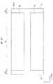
図33〜図35は、本実施の形態の半導体レーザの構成を示す断面図であり、図36は、本実施の形態の半導体レーザの構成を示す平面図である。例えば、図33は、図36のA−A部に、図34は、図36のB−B部に、図35は、図36のC−C部に対応する。[Description of structure]
33 to 35 are cross-sectional views illustrating the configuration of the semiconductor laser according to the present embodiment, and FIG. 36 is a plan view illustrating the configuration of the semiconductor laser according to the present embodiment. For example, FIG. 33 corresponds to the AA portion of FIG. 36, FIG. 34 corresponds to the BB portion of FIG. 36, and FIG. 35 corresponds to the CC portion of FIG.
図33〜図36に示すように、本実施の形態の半導体レーザは、p型コンタクト層PCNTおよびp型クラッド層PCLDがライン状の積層部となっている。このようなライン状の積層部をリッジストライプ構造という場合がある。 As shown in FIGS. 33 to 36, in the semiconductor laser according to the present embodiment, the p-type contact layer PCNT and the p-type cladding layer PCLD are line-shaped stacked portions. Such a line stack may be referred to as a ridge stripe structure.
本実施の形態の半導体レーザにおいて、n側電極NEL上のp型ガイド層PLGまでの構成は実施の形態1と同様である。 In the semiconductor laser of the present embodiment, the configuration up to the p-type guide layer PLG on the n-side electrode NEL is the same as that of the first embodiment.
例えば、本実施の形態の半導体レーザは、実施の形態1と同様に、基板として(0001)面から<1-100>方向に傾斜したオフ角を有するn型基板NSを用い、その上に順次積層された、複数の窒化物半導体層を有する。具体的には、実施の形態1の場合と同様に、n型基板NS上に、n型クラッド層NCLDが配置されている。n型基板NSおよびn型クラッド層NCLDの構成材料としては、実施の形態1と同様の材料を用いることができる。 For example, in the semiconductor laser according to the present embodiment, as in the first embodiment, an n-type substrate NS having an off angle inclined in the <1-100> direction from the (0001) plane is used as the substrate, and the semiconductor laser is sequentially formed thereon. A plurality of nitride semiconductor layers are stacked. Specifically, as in the case of the first embodiment, an n-type cladding layer NCLD is disposed on the n-type substrate NS. As the constituent materials of the n-type substrate NS and the n-type cladding layer NCLD, the same materials as those in the first embodiment can be used.
そして、n型クラッド層NCLD上には、電流ブロック層BLが配置されている。電流ブロック層BLの構成材料としては、実施の形態1と同様の材料を用いることができる。また、電流ブロック層BLの上面から見た平面形状は、実施の形態1と同様である(図12参照)。即ち、<1−100>方向に長辺を有する矩形状(四角形状)の2つの電流ブロック層BLが活性領域ACに形成される。2つの電流ブロック層BLは、電流狭窄領域となる領域1Aの両側にそれぞれ配置されている。電流ブロック層BL間には、n型クラッド層NCLDが露出している。 A current blocking layer BL is disposed on the n-type cladding layer NCLD. As a constituent material of the current block layer BL, the same material as that of the first embodiment can be used. Moreover, the planar shape seen from the upper surface of the current block layer BL is the same as that of the first embodiment (see FIG. 12). That is, two rectangular (rectangular) current blocking layers BL having long sides in the <1-100> direction are formed in the active region AC. The two current block layers BL are respectively arranged on both sides of the
さらに、実施の形態1と同様に、電流ブロック層BLおよびn型クラッド層NCLD上に、n型光ガイド層NLG、活性層MQWおよびp型光ガイド層PLGが順次配置されている。これらの層は、実施の形態1の場合と同様に、それぞれ複数の層厚部を有する。例えば、活性層MQWの窓領域WAの層厚TMQWWは、活性領域ACの領域1A(電流狭窄領域)の層厚TMQW1Aより小さい(TMQWW<TMQW1A)。また、これらの層の構成材料としては、実施の形態1と同様の材料を用いることができる。 Further, similarly to the first embodiment, the n-type light guide layer NLG, the active layer MQW, and the p-type light guide layer PLG are sequentially disposed on the current block layer BL and the n-type cladding layer NCLD. Each of these layers has a plurality of layer thickness portions as in the case of the first embodiment. For example, the layer thickness TMQWW of the window region WA of the active layer MQW is smaller than the layer thickness TMQW1A of the
ここで、p型光ガイド層PLG上には、p型クラッド層PCLDおよびp型コンタクト層PCNTが配置されているが、これらの層は主として領域1Aに配置されている。このように、p型クラッド層PCLDおよびp型コンタクト層PCNTの積層部がライン状(図36のX方向に長辺を有する矩形状)に電流ブロック層BL間(領域1A)上に延在している(図33、図36参照)。 Here, the p-type cladding layer PCLD and the p-type contact layer PCNT are arranged on the p-type light guide layer PLG, and these layers are mainly arranged in the
そして、このライン状の積層部(リッジストライプ部)の側壁は、絶縁層(絶縁膜)ILで覆われている。この絶縁層ILは、リッジストライプ部の側壁からその両側のp型クラッド層PCLD上に配置されている。そして、最上層のp型コンタクト層PCNT上には、p側電極PELが配置され、n型基板NSの裏面には、n側電極NELが配置されている。これらの構成材料としては、実施の形態1と同様の材料を用いることができる。 The side walls of the line-shaped stacked portion (ridge stripe portion) are covered with an insulating layer (insulating film) IL. The insulating layer IL is disposed on the p-type cladding layer PCLD on both sides from the side wall of the ridge stripe portion. A p-side electrode PEL is disposed on the uppermost p-type contact layer PCNT, and an n-side electrode NEL is disposed on the back surface of the n-type substrate NS. As these constituent materials, the same materials as in the first embodiment can be used.
また、(0001)面から<1-100>方向に傾斜したオフ角を有する基板を用いることで、電流ブロック層BLの有無により、電流狭窄領域(領域1A)の活性層MQWより窓領域WAの活性層MQWを薄く形成することができる。これにより、光出射端面(CP)の光学損傷による端面破壊を抑制することができる。 Further, by using a substrate having an off angle inclined in the <1-100> direction from the (0001) plane, the window region WA is more than the active layer MQW in the current confinement region (
さらに、本実施の形態においては、電流ブロック層BLが形成されていない窓領域WAにおいても、リッジストライプ部により、横方向の光を閉じ込めることができ、窓領域WAでの導波路損失を低減することができる。これにより、ファーフィールドパターン(FFP:遠視野像)を良好にすることができる。 Furthermore, in this embodiment, even in the window area WA in which the current blocking layer BL is not formed, the light in the lateral direction can be confined by the ridge stripe portion, and the waveguide loss in the window area WA is reduced. be able to. Thereby, a far field pattern (FFP: far-field image) can be made favorable.
特に、ブロードストライプ型(領域1Aの幅が約5μm以上)のマルチモードのレーザ素子では導波路損失の影響は小さいが、ナローストライプ型(領域1Aの幅が約1μm〜2μm)のシングルモードのレーザ素子では導波路損失の影響が大きくなる恐れがあるため、本実施の形態のようなリッジストライプ構造を採用することが好ましい。 In particular, a multi-mode laser element of a broad stripe type (
[製法説明]
次いで、図37〜図39を参照しながら、本実施の形態の半導体レーザの製造方法を説明するとともに、当該半導体レーザの構成をより明確にする。図37〜図39は、本実施の形態の半導体レーザの製造工程を示す断面図である。[Product description]
Next, the method for manufacturing the semiconductor laser according to the present embodiment will be described with reference to FIGS. 37 to 39, and the configuration of the semiconductor laser will be clarified. 37 to 39 are cross-sectional views showing the manufacturing steps of the semiconductor laser of the present embodiment.
実施の形態1と同様にして、n型基板NS上に、n型クラッド層NCLD、電流ブロック層BL、n型光ガイド層NLG、活性層MQW、p型光ガイド層PLG、p型クラッド層PCLDおよびp型コンタクト層PCNTを順次形成する(図29参照)。 As in the first embodiment, an n-type cladding layer NCLD, a current blocking layer BL, an n-type light guide layer NLG, an active layer MQW, a p-type light guide layer PLG, and a p-type cladding layer PCLD are formed on the n-type substrate NS. Then, the p-type contact layer PCNT is sequentially formed (see FIG. 29).
次いで、図37に示すように、p型コンタクト層PCNT(p型GaN層)およびp型クラッド層PCLDをパターニングすることにより、リッジストライプ部を形成する。例えば、p型コンタクト層PCNT(p型GaN層)上に、ハードマスク(図示せず)を形成する。例えば、CVD法などを用いて、p型コンタクト層PCNT(p型GaN層)上に、酸化シリコン膜を、0.3μm程度の層厚で形成する。次いで、酸化シリコン膜上に、フォトレジスト膜(図示せず)を塗布した後、フォトリソグラフィ技術を用いてリッジストライプ部の形成領域にフォトレジスト膜を残存させる。次いで、フォトレジスト膜をマスクとして、ハードマスク(酸化シリコン膜)をエッチングする。エッチング法としては、ドライエッチング法およびウェットエッチング法のいずれを用いてもよい。次いで、フォトレジスト膜をアッシングなどにより除去し、ハードマスク(酸化シリコン膜)をマスクとして、p型コンタクト層PCNT(p型GaN層)およびp型クラッド層PCLDをドライエッチング法によりエッチングする(図37)。次いで、ハードマスクを除去する。これにより、幅約1μm〜2μmのリッジストライプ部(p型クラッド層PCLDおよびp型コンタクト層PCNTの積層部)を形成する。ここで言う幅は、例えば、図36におけるY方向の幅である。ここで、図37においては、p型クラッド層PCLDの途中までしかエッチングしていないが、p型光ガイド層PLGが露出するまでエッチングしてもよい。 Next, as shown in FIG. 37, the ridge stripe portion is formed by patterning the p-type contact layer PCNT (p-type GaN layer) and the p-type cladding layer PCLD. For example, a hard mask (not shown) is formed on the p-type contact layer PCNT (p-type GaN layer). For example, a silicon oxide film is formed with a layer thickness of about 0.3 μm on the p-type contact layer PCNT (p-type GaN layer) by using a CVD method or the like. Next, after applying a photoresist film (not shown) on the silicon oxide film, the photoresist film is left in the formation region of the ridge stripe portion by using a photolithography technique. Next, the hard mask (silicon oxide film) is etched using the photoresist film as a mask. As the etching method, either a dry etching method or a wet etching method may be used. Next, the photoresist film is removed by ashing or the like, and the p-type contact layer PCNT (p-type GaN layer) and the p-type cladding layer PCLD are etched by dry etching using a hard mask (silicon oxide film) as a mask (FIG. 37). ). Next, the hard mask is removed. Thus, a ridge stripe portion (a laminated portion of the p-type cladding layer PCLD and the p-type contact layer PCNT) having a width of about 1 μm to 2 μm is formed. The width referred to here is, for example, the width in the Y direction in FIG. Here, in FIG. 37, etching is performed only halfway through the p-type cladding layer PCLD, but etching may be performed until the p-type light guide layer PLG is exposed.
次いで、図38に示すように、リッジストライプ部(p型クラッド層PCLDおよびp型コンタクト層PCNTの積層部)およびp型クラッド層PCLD上に、絶縁層ILとして、例えば、酸化シリコン膜をCVD法などを用いて形成する。これにより、リッジストライプ部の上面および側面は、絶縁層IL(酸化シリコン膜)で覆われる。また、リッジストライプ部の両側のp型クラッド層PCLDが、絶縁層IL(酸化シリコン膜)で覆われる。 Next, as shown in FIG. 38, for example, a silicon oxide film is formed on the ridge stripe portion (laminated portion of the p-type cladding layer PCLD and the p-type contact layer PCNT) and the p-type cladding layer PCLD as an insulating layer IL by a CVD method. And so on. Thereby, the upper surface and the side surface of the ridge stripe part are covered with the insulating layer IL (silicon oxide film). In addition, the p-type cladding layer PCLD on both sides of the ridge stripe portion is covered with an insulating layer IL (silicon oxide film).
次いで、リッジストライプ部(p型クラッド層PCLDおよびp型コンタクト層PCNTの積層部)の上面の絶縁層ILを除去する。例えば、リッジストライプ部上に開口部を有するフォトレジスト膜(図示せず)をマスクとして、絶縁層ILをエッチングする。次いで、フォトレジスト膜をアッシングなどにより除去する。 Next, the insulating layer IL on the upper surface of the ridge stripe portion (laminated portion of the p-type cladding layer PCLD and the p-type contact layer PCNT) is removed. For example, the insulating layer IL is etched using a photoresist film (not shown) having an opening on the ridge stripe as a mask. Next, the photoresist film is removed by ashing or the like.
次いで、リッジストライプ部(p型コンタクト層PCNT)の上面にp側電極PELを形成する(図39)。 Next, a p-side electrode PEL is formed on the upper surface of the ridge stripe portion (p-type contact layer PCNT) (FIG. 39).
次いで、n型基板NSの裏面側を上面とし、n型基板NSの裏面を研磨することにより、n型基板NSを薄膜化する。例えば、n型基板NSを100μm程度の厚さとする。次いで、n型基板NSの裏面に、n側電極NELを形成する(図39)。この後、実施の形態1の場合と同様にして、チップ片を切り出す。 Next, the n-type substrate NS is thinned by polishing the back surface of the n-type substrate NS with the back side of the n-type substrate NS as the upper surface. For example, the n-type substrate NS is about 100 μm thick. Next, an n-side electrode NEL is formed on the back surface of the n-type substrate NS (FIG. 39). Thereafter, the chip piece is cut out in the same manner as in the first embodiment.
以上の工程により、本実施の形態の半導体レーザを形成することができる。 Through the above steps, the semiconductor laser of this embodiment can be formed.
このように、本実施の形態においても、実施の形態1と同様に、(0001)面から<1-100>方向に傾斜したオフ角を有する基板を用いることで、電流ブロック層BLの有無により、電流狭窄領域の活性層MQWより窓領域WAの活性層MQWを薄く形成することができ、光出射端面の光学損傷による端面破壊を抑制することができる。 Thus, in the present embodiment as well, in the same manner as in the first embodiment, by using a substrate having an off angle inclined in the <1-100> direction from the (0001) plane, the presence or absence of the current blocking layer BL is determined. The active layer MQW in the window region WA can be formed thinner than the active layer MQW in the current confinement region, and end face destruction due to optical damage of the light emitting end face can be suppressed.
さらに、本実施の形態においては、電流ブロック層BLが形成されていない窓領域WAにおいても、リッジストライプ部により、横方向の光を閉じ込めることができ、窓領域WAでの導波路損失を低減することができる。 Furthermore, in this embodiment, even in the window area WA in which the current blocking layer BL is not formed, the light in the lateral direction can be confined by the ridge stripe portion, and the waveguide loss in the window area WA is reduced. be able to.
このように、特性の良好な半導体レーザを製造することができる。 Thus, a semiconductor laser with good characteristics can be manufactured.
(実施の形態3)
実施の形態1においては、領域3Aに電流ブロック層BLを形成していないが(図12参照)、電流ブロック層BLを領域2Aから領域3Aまで延在させてもよい。(Embodiment 3)
In the first embodiment, the current block layer BL is not formed in the
また、実施の形態1においては、窓領域WAを劈開面CPに沿って、チップ領域のY方向全域に延在させたが(図4参照)、窓領域WAは、光出射部を含み、領域1Aの幅より広い幅を有する領域であればよく、チップ領域のY方向全域に延在させる必要はない。 In the first embodiment, the window area WA extends along the cleavage plane CP over the entire Y direction of the chip area (see FIG. 4). However, the window area WA includes a light emitting portion, Any region having a width wider than 1A may be used, and it is not necessary to extend the entire Y direction of the chip region.
(第1例)
図40は、本実施の形態の半導体レーザの第1例を示す平面図である。図40に示すように、本実施の形態においては、電流ブロック層BLが図12に示す領域2Aおよび領域3Aに形成されている。電流ブロック層BL以外の構成は、実施の形態1の場合と同様であるためその説明を省略する。また、本実施の形態の半導体レーザの製造工程は、電流ブロック層BLを図40に示す形状にエッチングする以外は、実施の形態1と同様である。(First example)
FIG. 40 is a plan view showing a first example of the semiconductor laser according to the present embodiment. As shown in FIG. 40, in the present embodiment, current blocking layer BL is formed in
このように、電流ブロック層BLを、チップ領域(n型クラッド層NCLD)のX方向に延在する端部(辺、図中の横の辺)まで、Y方向に伸ばしてもよい。 In this way, the current blocking layer BL may be extended in the Y direction to the end (side, side in the drawing) extending in the X direction of the chip region (n-type cladding layer NCLD).
(第2例)
図41は、本実施の形態の半導体レーザの第2例を示す平面図である。図41に示すように、本実施の形態においては、窓領域WAが、電流ブロック層BL間の中心線部(光出射部)を含み、Y方向に領域1Aの幅より広い幅Wを有する領域となっている。そして、チップ領域のY方向に延在する辺(線CL、劈開面CP)の両端部には、電流ブロック層BLが配置されている。(Second example)
FIG. 41 is a plan view showing a second example of the semiconductor laser according to the present embodiment. As shown in FIG. 41, in the present embodiment, window region WA includes a center line portion (light emitting portion) between current blocking layers BL, and has a width W wider than the width of
このように、窓領域WAのY方向の幅Wを、電流ブロック層BL間(第1領域1A)のY方向の幅より大きくしつつ、窓領域WAを、チップ領域のY方向に延在する辺(線CL、劈開面CP)の一部に沿って配置してもよい。 As described above, the window region WA extends in the Y direction of the chip region while the width W in the Y direction of the window region WA is made larger than the width in the Y direction between the current blocking layers BL (
本実施の形態の第1例および第2例においても、実施の形態1と同様の効果を奏する。また、実施の形態2の構成に、上記第1例または第2例で示した電流ブロック層BLの構成を適用してもよい。 In the first example and the second example of the present embodiment, the same effects as those of the first embodiment are obtained. Further, the configuration of the current blocking layer BL shown in the first example or the second example may be applied to the configuration of the second embodiment.
(応用例)
上記実施の形態において説明した半導体レーザの適用範囲に制限はないが、例えば、光ディスク装置に適用することができる。光ディスク装置は、BD(Blu-lay)などの光ディスクから情報を読み取る装置である。光ディスクに記録されている信号の読み出し動作は、光ピックアップで行われる。光ピックアップは、光ディスクのデータの読み出しを行うための光源および受光部を有する。この光ピックアップの光源として、上記実施の形態において説明した半導体レーザを用いることで、光出射端面の光学損傷を抑制でき、光源の特性を向上させることができる。(Application examples)
The application range of the semiconductor laser described in the above embodiment is not limited, but can be applied to, for example, an optical disc apparatus. An optical disc device is a device that reads information from an optical disc such as a BD (Blu-lay). The read operation of the signal recorded on the optical disc is performed by an optical pickup. The optical pickup includes a light source and a light receiving unit for reading data from the optical disc. By using the semiconductor laser described in the above embodiment as the light source of this optical pickup, optical damage on the light emitting end face can be suppressed, and the characteristics of the light source can be improved.
以上、本発明者によってなされた発明を実施の形態に基づき具体的に説明したが、本発明は上記実施の形態に限定されるものではなく、その要旨を逸脱しない範囲で種々変更可能であることはいうまでもない。 As mentioned above, the invention made by the present inventor has been specifically described based on the embodiment. However, the present invention is not limited to the above embodiment, and various modifications can be made without departing from the scope of the invention. Needless to say.
例えば、上記実施の形態1〜3においては、III−V族化合物半導体のうち、窒化物半導体を用いた半導体レーザの場合について説明したが、上記実施の形態1〜3を他のIII−V族化合物半導体を用いた半導体レーザに適用してもよい。 For example, in the first to third embodiments, the case of a semiconductor laser using a nitride semiconductor among the III-V compound semiconductors has been described. You may apply to the semiconductor laser using a compound semiconductor.
1A 領域
2A 領域
3A 領域
AC 活性領域
BL 電流ブロック層
CL 線
CP 劈開面
IL 絶縁層
L レーザ光
MQW 活性層
NCLD n型クラッド層
NEL n側電極
NLG n型光ガイド層
NS n型基板
OA 開口部
PCLD p型クラッド層
PCNT p型コンタクト層
PEL p側電極
PLG p型光ガイド層
TMQW1A 層厚
TMQW2A 層厚
TMQWW 層厚
TNLG1A 層厚
TNLG2A 層厚
TNLGW 層厚
TPLG1A 層厚
TPLG2A 層厚
TPLGW 層厚
WA 窓領域
W 幅
Claims (20)
Translated fromJapanese前記基板の主面の上方に配置された第1窒化物半導体層と、
前記第1窒化物半導体層の上方に配置された第2窒化物半導体層と、
前記第2窒化物半導体層の上方に配置された第3窒化物半導体層と、
前記第1窒化物半導体層と前記第2窒化物半導体層との間に配置された第4窒化物半導体層と、
前記第2窒化物半導体層が露出する側面と、
を有し、
前記側面は、第1方向に延在し、
前記第4窒化物半導体層は、前記第1方向と交差する第2方向に延在する第1領域の両側の第2領域に、前記側面から後退して配置され、
前記第1窒化物半導体層は、前記第2窒化物半導体層よりバンドギャップが大きく、第1導電型であり、
前記第3窒化物半導体層は、前記第2窒化物半導体層よりバンドギャップが大きく、前記第1導電型と逆導電型の第2導電型であり、
前記第4窒化物半導体層は、前記第3窒化物半導体層よりバンドギャップが大きく、Alを含有し、
前記基板の前記主面は、(0001)面から<1-100>方向にオフ角を有し、
前記第2窒化物半導体層の前記側面から前記第4窒化物半導体層の端部までの第3領域の層厚は、前記第1領域の層厚より小さい、半導体装置。A substrate,
A first nitride semiconductor layer disposed above a main surface of the substrate;
A second nitride semiconductor layer disposed above the first nitride semiconductor layer;
A third nitride semiconductor layer disposed above the second nitride semiconductor layer;
A fourth nitride semiconductor layer disposed between the first nitride semiconductor layer and the second nitride semiconductor layer;
A side surface from which the second nitride semiconductor layer is exposed;
Have
The side surface extends in a first direction;
The fourth nitride semiconductor layer is disposed in a second region on both sides of the first region extending in the second direction intersecting the first direction, and is retracted from the side surface.
The first nitride semiconductor layer has a larger band gap than the second nitride semiconductor layer, and is of a first conductivity type,
The third nitride semiconductor layer has a larger band gap than the second nitride semiconductor layer, and is a second conductivity type opposite to the first conductivity type,
The fourth nitride semiconductor layer has a larger band gap than the third nitride semiconductor layer, contains Al,
The main surface of the substrate has an off angle in the <1-100> direction from the (0001) plane,
A semiconductor device, wherein a layer thickness of a third region from the side surface of the second nitride semiconductor layer to an end portion of the fourth nitride semiconductor layer is smaller than a layer thickness of the first region.
前記第2窒化物半導体層と前記第4窒化物半導体層との間に配置された第5窒化物半導体層を有し、
前記第2窒化物半導体層は、前記第5窒化物半導体層上に配置されている、半導体装置。The semiconductor device according to claim 1,
A fifth nitride semiconductor layer disposed between the second nitride semiconductor layer and the fourth nitride semiconductor layer;
The semiconductor device, wherein the second nitride semiconductor layer is disposed on the fifth nitride semiconductor layer.
前記第5窒化物半導体層の前記第3領域の層厚は、前記第1領域の層厚より小さい、半導体装置。The semiconductor device according to claim 2,
The semiconductor device, wherein a thickness of the third region of the fifth nitride semiconductor layer is smaller than a thickness of the first region.
前記第2窒化物半導体層と前記第3窒化物半導体層との間に配置された第6窒化物半導体層を有し、
前記第6窒化物半導体層は、前記第2窒化物半導体層上に配置されている、半導体装置。The semiconductor device according to claim 1,
A sixth nitride semiconductor layer disposed between the second nitride semiconductor layer and the third nitride semiconductor layer;
The semiconductor device, wherein the sixth nitride semiconductor layer is disposed on the second nitride semiconductor layer.
前記第2方向は、前記<1-100>方向である、半導体装置。The semiconductor device according to claim 1,
The semiconductor device, wherein the second direction is the <1-100> direction.
前記第4窒化物半導体層の平面形状は、前記<1-100>方向に長辺を有する四角形状である、半導体装置。The semiconductor device according to claim 5.
The planar shape of the fourth nitride semiconductor layer is a semiconductor device having a rectangular shape having long sides in the <1-100> direction.
前記第4窒化物半導体層は、窒化アルミニウム層または窒化アルミニウム・ガリウム層である、半導体装置。The semiconductor device according to claim 1,
The semiconductor device, wherein the fourth nitride semiconductor layer is an aluminum nitride layer or an aluminum nitride / gallium layer.
前記第1窒化物半導体層は、n型不純物が導入された窒化アルミニウム・ガリウム層であり、
前記第2窒化物半導体層は、インジウム組成の異なる第1窒化インジウム・ガリウム層と第2窒化インジウム・ガリウム層とを交互に積層した積層体であり、
前記第3窒化物半導体層は、p型不純物が導入された窒化アルミニウム・ガリウム層を有する、半導体装置。The semiconductor device according to claim 7.
The first nitride semiconductor layer is an aluminum gallium nitride layer into which an n-type impurity is introduced,
The second nitride semiconductor layer is a laminate in which first indium gallium nitride layers and second indium gallium nitride layers having different indium compositions are alternately laminated,
The third nitride semiconductor layer is a semiconductor device having an aluminum gallium nitride layer into which a p-type impurity is introduced.
前記第3領域は、前記側面の全域に沿って配置されている、半導体装置。The semiconductor device according to claim 1,
The semiconductor device, wherein the third region is disposed along the entire side surface.
前記第4窒化物半導体層は、前記第1窒化物半導体層の端部であって、前記第2方向に延在する端部まで延在している、半導体装置。The semiconductor device according to claim 9.
The fourth nitride semiconductor layer is a semiconductor device that extends to an end portion of the first nitride semiconductor layer that extends in the second direction.
前記第3領域は、前記側面の一部に沿って、前記側面の一部と前記第1領域との間に配置され、
前記第3領域の前記第1方向の幅は、前記第1領域の前記第1方向の幅より大きい、半導体装置。The semiconductor device according to claim 1,
The third region is disposed between a part of the side surface and the first region along a part of the side surface,
The width of the third region in the first direction is larger than the width of the first region in the first direction.
前記第3窒化物半導体層は、前記第1領域上に、前記<1-100>方向にライン状に、前記側面まで延在している、半導体装置。The semiconductor device according to claim 1,
The third nitride semiconductor layer is a semiconductor device that extends to the side surface in a line shape in the <1-100> direction on the first region.
前記ライン状の前記第3窒化物半導体層の前記第1方向の幅は、前記第1領域の前記第1方向の幅より小さい、半導体装置。The semiconductor device according to claim 12, wherein
A width of the line-shaped third nitride semiconductor layer in the first direction is smaller than a width of the first region in the first direction.
(b)前記第1窒化物半導体層の上方に、第2窒化物半導体層を形成する工程、
(c)前記第2窒化物半導体層をエッチングすることにより、前記第1窒化物半導体層の第1方向に延在する側面線と交差する第2方向に延在する第1領域の両側の第2領域に、前記側面線から後退して配置されるように前記第2窒化物半導体層を残存させる工程、
(d)前記第1窒化物半導体層および前記第2窒化物半導体層の上方に、第3窒化物半導体層を形成する工程、
を有する、半導体装置の製造方法。(A) forming a first nitride semiconductor layer above a substrate whose main surface has an off angle in the <1-100> direction from the (0001) plane;
(B) forming a second nitride semiconductor layer above the first nitride semiconductor layer;
(C) by etching the second nitride semiconductor layer, the second nitride semiconductor layer is formed on both sides of the first region extending in the second direction intersecting the side line extending in the first direction of the first nitride semiconductor layer. A step of leaving the second nitride semiconductor layer so as to be disposed in two regions so as to recede from the side line;
(D) forming a third nitride semiconductor layer above the first nitride semiconductor layer and the second nitride semiconductor layer;
A method for manufacturing a semiconductor device, comprising:
前記(d)工程は、前記第3窒化物半導体層を結晶成長させる工程で、前記側面線から前記第2窒化物半導体層の端部までの第3領域の層厚が、前記第1領域の層厚より小さい、前記3窒化物半導体層を形成する工程である、半導体装置の製造方法。15. The method of manufacturing a semiconductor device according to claim 14,
The step (d) is a step of crystal-growing the third nitride semiconductor layer, and the layer thickness of the third region from the side line to the end of the second nitride semiconductor layer is equal to that of the first region. A method for manufacturing a semiconductor device, the step of forming the trinitride semiconductor layer having a thickness smaller than that of the layer.
前記(d)工程の後に、
(e)前記第3窒化物半導体層の上方に、第4窒化物半導体層を形成する工程、を有する、半導体装置の製造方法。In the manufacturing method of the semiconductor device according to claim 15,
After the step (d),
(E) forming a fourth nitride semiconductor layer above the third nitride semiconductor layer; and a method for manufacturing a semiconductor device.
前記(e)工程の後に、
(f)前記第4窒化物半導体層をエッチングすることにより、前記第1領域上にライン状の前記第4窒化物半導体層を残存させる工程、を有する、半導体装置の製造方法。In the manufacturing method of the semiconductor device according to claim 16,
After the step (e),
(F) A method of manufacturing a semiconductor device, comprising: etching the fourth nitride semiconductor layer to leave the line-shaped fourth nitride semiconductor layer on the first region.
前記ライン状の前記第4窒化物半導体層の前記第1方向の幅は、前記第1領域の前記第1方向の幅より小さい、半導体装置の製造方法。In the manufacturing method of the semiconductor device according to claim 16,
The width of the line-shaped fourth nitride semiconductor layer in the first direction is smaller than the width of the first region in the first direction.
前記第2窒化物半導体層の平面形状は、前記<1-100>方向に長辺を有する四角形状である、半導体装置の製造方法。15. The method of manufacturing a semiconductor device according to claim 14,
The planar shape of the second nitride semiconductor layer is a method for manufacturing a semiconductor device, which is a quadrangular shape having long sides in the <1-100> direction.
前記第4窒化物半導体層は、窒化アルミニウム層または窒化アルミニウム・ガリウム層である、半導体装置の製造方法。15. The method of manufacturing a semiconductor device according to claim 14,
The method of manufacturing a semiconductor device, wherein the fourth nitride semiconductor layer is an aluminum nitride layer or an aluminum nitride / gallium layer.
Priority Applications (3)
| Application Number | Priority Date | Filing Date | Title |
|---|---|---|---|
| JP2014112268AJP2015226045A (en) | 2014-05-30 | 2014-05-30 | Semiconductor device and method of manufacturing the same |
| US14/697,908US9368940B2 (en) | 2014-05-30 | 2015-04-28 | Semiconductor device and manufacturing method of semiconductor device |
| CN201510288891.XACN105186284A (en) | 2014-05-30 | 2015-05-29 | Semiconductor device and manufacturing method of semiconductor device |
Applications Claiming Priority (1)
| Application Number | Priority Date | Filing Date | Title |
|---|---|---|---|
| JP2014112268AJP2015226045A (en) | 2014-05-30 | 2014-05-30 | Semiconductor device and method of manufacturing the same |
Publications (1)
| Publication Number | Publication Date |
|---|---|
| JP2015226045Atrue JP2015226045A (en) | 2015-12-14 |
Family
ID=54702878
Family Applications (1)
| Application Number | Title | Priority Date | Filing Date |
|---|---|---|---|
| JP2014112268APendingJP2015226045A (en) | 2014-05-30 | 2014-05-30 | Semiconductor device and method of manufacturing the same |
Country Status (3)
| Country | Link |
|---|---|
| US (1) | US9368940B2 (en) |
| JP (1) | JP2015226045A (en) |
| CN (1) | CN105186284A (en) |
Families Citing this family (5)
| Publication number | Priority date | Publication date | Assignee | Title |
|---|---|---|---|---|
| FR3002654A1 (en) | 2013-02-26 | 2014-08-29 | St Microelectronics Sa | OPTICAL MODULATOR WITH AUTOMATIC POLARIZATION CORRECTION |
| JP2017050318A (en)* | 2015-08-31 | 2017-03-09 | ルネサスエレクトロニクス株式会社 | Semiconductor device |
| US10541514B2 (en)* | 2016-02-25 | 2020-01-21 | Ngk Insulators, Ltd. | Surface-emitting device, vertical external-cavity surface-emitting laser, and method for manufacturing surface-emitting device |
| TWI609541B (en)* | 2016-12-12 | 2017-12-21 | 聯亞光電工業股份有限公司 | Semicondoctor laser apparatus |
| DE102019118993A1 (en)* | 2019-07-12 | 2021-01-14 | OSRAM Opto Semiconductors Gesellschaft mit beschränkter Haftung | EDGE-EMITTING SEMI-CONDUCTIVE LASER DIODE AND METHOD FOR MANUFACTURING SUCH |
Family Cites Families (14)
| Publication number | Priority date | Publication date | Assignee | Title |
|---|---|---|---|---|
| JP2000196188A (en) | 1998-12-25 | 2000-07-14 | Toshiba Corp | Semiconductor laser device and method of manufacturing the same |
| JP2003060298A (en) | 2001-08-08 | 2003-02-28 | Nichia Chem Ind Ltd | Method of manufacturing semiconductor light emitting device and semiconductor light emitting device |
| JP3779248B2 (en)* | 2002-08-27 | 2006-05-24 | 株式会社東芝 | Semiconductor laser element |
| JP2004296634A (en)* | 2003-03-26 | 2004-10-21 | Sharp Corp | Semiconductor laser device and optical disk device |
| JP4540347B2 (en)* | 2004-01-05 | 2010-09-08 | シャープ株式会社 | Nitride semiconductor laser device and manufacturing method thereof |
| US7339255B2 (en)* | 2004-08-24 | 2008-03-04 | Kabushiki Kaisha Toshiba | Semiconductor device having bidirectionally inclined toward <1-100> and <11-20> relative to {0001} crystal planes |
| JP4772314B2 (en)* | 2004-11-02 | 2011-09-14 | シャープ株式会社 | Nitride semiconductor device |
| US8368183B2 (en)* | 2004-11-02 | 2013-02-05 | Sharp Kabushiki Kaisha | Nitride semiconductor device |
| US7652299B2 (en)* | 2005-02-14 | 2010-01-26 | Showa Denko K.K. | Nitride semiconductor light-emitting device and method for fabrication thereof |
| JP2007234796A (en)* | 2006-02-28 | 2007-09-13 | Matsushita Electric Ind Co Ltd | Nitride semiconductor laser device and manufacturing method thereof |
| JP2010199520A (en)* | 2009-02-27 | 2010-09-09 | Renesas Electronics Corp | Semiconductor laser, and method of manufacturing the same |
| JP2011124253A (en)* | 2009-12-08 | 2011-06-23 | Sony Corp | Method of manufacturing semiconductor laser, semiconductor laser, optical disk device, method of manufacturing semiconductor device and semiconductor device |
| CN103444021B (en)* | 2011-03-24 | 2016-04-27 | 松下知识产权经营株式会社 | Nitride semiconductor light emitting element |
| JP5664627B2 (en)* | 2012-10-16 | 2015-02-04 | 住友電気工業株式会社 | Group III nitride semiconductor laser device, method of manufacturing group III nitride semiconductor laser device, method of evaluating end face for optical resonator of group III nitride semiconductor laser device, method of evaluating scribe groove |
- 2014
- 2014-05-30JPJP2014112268Apatent/JP2015226045A/enactivePending
- 2015
- 2015-04-28USUS14/697,908patent/US9368940B2/ennot_activeExpired - Fee Related
- 2015-05-29CNCN201510288891.XApatent/CN105186284A/enactivePending
Also Published As
| Publication number | Publication date |
|---|---|
| US9368940B2 (en) | 2016-06-14 |
| CN105186284A (en) | 2015-12-23 |
| US20150349496A1 (en) | 2015-12-03 |
Similar Documents
| Publication | Publication Date | Title |
|---|---|---|
| US6925101B2 (en) | Semiconductor laser device, and method of manufacturing the same | |
| US11677213B1 (en) | Systems for photonic integration in non-polar and semi-polar oriented wave-guided optical devices | |
| CN110402524A (en) | Semiconductor laser device, semiconductor laser module, and laser source system for welding | |
| JPWO2009078482A1 (en) | Semiconductor light emitting device | |
| JP2007266575A (en) | Semiconductor laser element and semiconductor laser device | |
| JP5247444B2 (en) | Semiconductor laser device | |
| US9368940B2 (en) | Semiconductor device and manufacturing method of semiconductor device | |
| JP3716974B2 (en) | Semiconductor laser device and manufacturing method thereof | |
| JP5093033B2 (en) | Semiconductor laser manufacturing method, semiconductor laser, optical pickup and optical disc apparatus | |
| CN102804416B (en) | Semiconductor light emitting element and method for manufacturing same | |
| CN101540477A (en) | Nitride semiconductor device and fabrication method thereof | |
| JP3933637B2 (en) | Gallium nitride semiconductor laser device | |
| JP6224514B2 (en) | Semiconductor device | |
| JP4146881B2 (en) | Nitride semiconductor light-emitting device, epi-wafer and method of manufacturing the same | |
| JP2011124253A (en) | Method of manufacturing semiconductor laser, semiconductor laser, optical disk device, method of manufacturing semiconductor device and semiconductor device | |
| JP5079613B2 (en) | Nitride-based semiconductor laser device and manufacturing method thereof | |
| JP2007049209A (en) | Semiconductor optical device device and manufacturing method thereof | |
| JP2001057458A (en) | Semiconductor light emitting device | |
| JP3849876B2 (en) | Semiconductor laser device and manufacturing method thereof | |
| JP3872627B2 (en) | Multi-beam type semiconductor optical device | |
| JP2011142147A (en) | Edge-emitting semiconductor light-emitting element, method of manufacturing the same, image display device, and information recording and reproducing device | |
| JP5074863B2 (en) | Nitride semiconductor light-emitting device, epi-wafer and method of manufacturing the same | |
| CN100375349C (en) | Semiconductor laser element and method for manufacturing the same | |
| JP2001291930A (en) | Semiconductor optical device | |
| JP2001077475A (en) | Semiconductor laser |