JP2015207604A - Wafer processing method - Google Patents
Wafer processing methodDownload PDFInfo
- Publication number
- JP2015207604A JP2015207604AJP2014085822AJP2014085822AJP2015207604AJP 2015207604 AJP2015207604 AJP 2015207604AJP 2014085822 AJP2014085822 AJP 2014085822AJP 2014085822 AJP2014085822 AJP 2014085822AJP 2015207604 AJP2015207604 AJP 2015207604A
- Authority
- JP
- Japan
- Prior art keywords
- wafer
- substrate
- division
- forming step
- cutting
- Prior art date
- Legal status (The legal status is an assumption and is not a legal conclusion. Google has not performed a legal analysis and makes no representation as to the accuracy of the status listed.)
- Pending
Links
Images


Classifications
- H—ELECTRICITY
- H01—ELECTRIC ELEMENTS
- H01L—SEMICONDUCTOR DEVICES NOT COVERED BY CLASS H10
- H01L21/00—Processes or apparatus adapted for the manufacture or treatment of semiconductor or solid state devices or of parts thereof
- H01L21/70—Manufacture or treatment of devices consisting of a plurality of solid state components formed in or on a common substrate or of parts thereof; Manufacture of integrated circuit devices or of parts thereof
- H01L21/77—Manufacture or treatment of devices consisting of a plurality of solid state components or integrated circuits formed in, or on, a common substrate
- H01L21/78—Manufacture or treatment of devices consisting of a plurality of solid state components or integrated circuits formed in, or on, a common substrate with subsequent division of the substrate into plural individual devices
- H—ELECTRICITY
- H01—ELECTRIC ELEMENTS
- H01L—SEMICONDUCTOR DEVICES NOT COVERED BY CLASS H10
- H01L21/00—Processes or apparatus adapted for the manufacture or treatment of semiconductor or solid state devices or of parts thereof
- H01L21/02—Manufacture or treatment of semiconductor devices or of parts thereof
- H01L21/04—Manufacture or treatment of semiconductor devices or of parts thereof the devices having potential barriers, e.g. a PN junction, depletion layer or carrier concentration layer
- H01L21/18—Manufacture or treatment of semiconductor devices or of parts thereof the devices having potential barriers, e.g. a PN junction, depletion layer or carrier concentration layer the devices having semiconductor bodies comprising elements of Group IV of the Periodic Table or AIIIBV compounds with or without impurities, e.g. doping materials
- H01L21/26—Bombardment with radiation
- H01L21/263—Bombardment with radiation with high-energy radiation
- H01L21/268—Bombardment with radiation with high-energy radiation using electromagnetic radiation, e.g. laser radiation
- H—ELECTRICITY
- H01—ELECTRIC ELEMENTS
- H01L—SEMICONDUCTOR DEVICES NOT COVERED BY CLASS H10
- H01L21/00—Processes or apparatus adapted for the manufacture or treatment of semiconductor or solid state devices or of parts thereof
- H01L21/02—Manufacture or treatment of semiconductor devices or of parts thereof
- H01L21/04—Manufacture or treatment of semiconductor devices or of parts thereof the devices having potential barriers, e.g. a PN junction, depletion layer or carrier concentration layer
- H01L21/18—Manufacture or treatment of semiconductor devices or of parts thereof the devices having potential barriers, e.g. a PN junction, depletion layer or carrier concentration layer the devices having semiconductor bodies comprising elements of Group IV of the Periodic Table or AIIIBV compounds with or without impurities, e.g. doping materials
- H01L21/30—Treatment of semiconductor bodies using processes or apparatus not provided for in groups H01L21/20 - H01L21/26
- H01L21/302—Treatment of semiconductor bodies using processes or apparatus not provided for in groups H01L21/20 - H01L21/26 to change their surface-physical characteristics or shape, e.g. etching, polishing, cutting
- H01L21/304—Mechanical treatment, e.g. grinding, polishing, cutting
- H01L21/3043—Making grooves, e.g. cutting
- H—ELECTRICITY
- H01—ELECTRIC ELEMENTS
- H01L—SEMICONDUCTOR DEVICES NOT COVERED BY CLASS H10
- H01L21/00—Processes or apparatus adapted for the manufacture or treatment of semiconductor or solid state devices or of parts thereof
- H01L21/67—Apparatus specially adapted for handling semiconductor or electric solid state devices during manufacture or treatment thereof; Apparatus specially adapted for handling wafers during manufacture or treatment of semiconductor or electric solid state devices or components ; Apparatus not specifically provided for elsewhere
- H01L21/67005—Apparatus not specifically provided for elsewhere
- H01L21/67011—Apparatus for manufacture or treatment
- H01L21/67092—Apparatus for mechanical treatment
- H—ELECTRICITY
- H01—ELECTRIC ELEMENTS
- H01L—SEMICONDUCTOR DEVICES NOT COVERED BY CLASS H10
- H01L21/00—Processes or apparatus adapted for the manufacture or treatment of semiconductor or solid state devices or of parts thereof
- H01L21/67—Apparatus specially adapted for handling semiconductor or electric solid state devices during manufacture or treatment thereof; Apparatus specially adapted for handling wafers during manufacture or treatment of semiconductor or electric solid state devices or components ; Apparatus not specifically provided for elsewhere
- H01L21/67005—Apparatus not specifically provided for elsewhere
- H01L21/67011—Apparatus for manufacture or treatment
- H01L21/67132—Apparatus for placing on an insulating substrate, e.g. tape
Landscapes
- Engineering & Computer Science (AREA)
- Physics & Mathematics (AREA)
- Condensed Matter Physics & Semiconductors (AREA)
- General Physics & Mathematics (AREA)
- Manufacturing & Machinery (AREA)
- Computer Hardware Design (AREA)
- Microelectronics & Electronic Packaging (AREA)
- Power Engineering (AREA)
- High Energy & Nuclear Physics (AREA)
- Electromagnetism (AREA)
- Optics & Photonics (AREA)
- Health & Medical Sciences (AREA)
- Toxicology (AREA)
- Dicing (AREA)
- Laser Beam Processing (AREA)
- Mechanical Treatment Of Semiconductor (AREA)
Abstract
Translated fromJapaneseDescription
Translated fromJapanese本発明は、ウェーハの加工方法に関し、特に、層間絶縁膜として低誘電率絶縁膜(Low−k膜)を使用したウェーハの加工方法に関する。 The present invention relates to a wafer processing method, and more particularly, to a wafer processing method using a low dielectric constant insulating film (Low-k film) as an interlayer insulating film.
半導体デバイス製造プロセスにおいては、略円板形状であるシリコンウェーハ、ガリウム砒素ウェーハ等の半導体ウェーハの表面に格子状に形成されたストリートと呼ばれる分割予定ラインによって複数の領域が区画され、区画された各領域にIC、LSI等のデバイスを形成する。 In the semiconductor device manufacturing process, a plurality of regions are defined by divided planned lines called streets formed in a lattice shape on the surface of a semiconductor wafer such as a silicon wafer or a gallium arsenide wafer having a substantially disk shape, A device such as an IC or LSI is formed in the region.
このような半導体ウェーハは研削装置によって裏面が研削されて所定の厚みに加工された後、切削装置又はレーザ加工装置によって個々のデバイスに分割され、分割されたデバイスは携帯電話、パソコン等の各種電気機器に広く利用されている。 After such a semiconductor wafer is ground to a predetermined thickness by a grinding device and then processed into a predetermined thickness, it is divided into individual devices by a cutting device or a laser processing device. Widely used in equipment.
切削装置としては一般にダイシング装置と呼ばれる切削装置が用いられており、この切削装置ではダイアモンドやCBN等の超砥粒をメタルやレジンで固めて厚さ20〜30μmの切刃を有する切削ブレードが約30000rpm等の高速で回転しつつ半導体ウェーハへ切り込むことで切削が遂行される。 As a cutting device, a cutting device generally called a dicing device is used. In this cutting device, a cutting blade having a cutting blade having a thickness of 20 to 30 μm is obtained by hardening superabrasive grains such as diamond and CBN with metal or resin. Cutting is performed by cutting into a semiconductor wafer while rotating at a high speed such as 30000 rpm.
半導体ウェーハの表面に形成された半導体デバイスは、金属配線が何層にも積層されて信号を伝達しており、各金属配線間は主にSiO2から形成された層間絶縁膜により絶縁されている。A semiconductor device formed on the surface of a semiconductor wafer has a plurality of layers of metal wirings that transmit signals, and each metal wiring is insulated by an interlayer insulating film formed mainly of SiO2 . .
近年、構造の微細化に伴い、配線間距離が近くなり、近接する配線間の電気容量は大きくなってきている。これに起因して信号の遅延が発生し、消費電力が増加するという問題が顕著になってきている。 In recent years, with the miniaturization of the structure, the distance between wirings has become shorter, and the electric capacity between adjacent wirings has increased. Due to this, a problem that signal delay occurs and power consumption increases has become prominent.
各層間の寄生容量を軽減すべく、デバイス(回路)形成時に各層間を絶縁する層間絶縁膜として従来は主にSiO2絶縁膜を採用していたが、最近になりSiO2絶縁膜よりも誘電率の低い低誘電率絶縁膜(Low−k膜)が採用されるようになってきている。In order to reduce the parasitic capacitance between the layers, the device (circuit) prior to each layer when forming an interlayer insulating film for insulating primarily had adopted the SiO2 insulating film, than recently become SiO2 insulating film dielectric A low dielectric constant insulating film (Low-k film) having a low rate has been adopted.
低誘電率絶縁膜としては、SiO2膜(誘電率k=4.1)よりも誘電率が低い(例えばk=2.5乃至3.6程度)材料、例えばSiOC,SiLK等の無機物系の膜、ポリイミド系、パリレン系、ポリテトラフルオロエチレン系等のポリマー膜である有機物系の膜、及びメチル含有ポリシロキサン等のポーラスシリカ膜を挙げることができる。As the low dielectric constant insulating film, a material having a dielectric constant lower than that of the SiO2 film (dielectric constant k = 4.1) (for example, about k = 2.5 to 3.6), for example, an inorganic material such as SiOC, SiLK, etc. Examples thereof include organic films such as films, polyimide-based, parylene-based, and polytetrafluoroethylene-based polymer films, and porous silica films such as methyl-containing polysiloxane.
このような低誘電率絶縁膜を含む積層体を切削ブレードにより分割予定ラインに沿って切削すると、低誘電率絶縁膜は雲母のように非常に脆いことから積層体が剥離するという問題が生じる。 When a laminated body including such a low dielectric constant insulating film is cut along a line to be divided by a cutting blade, the low dielectric constant insulating film is very brittle like mica, which causes a problem that the laminated body is peeled off.
この問題を解決するために、特開2007−173475号公報では、予め分割予定ライン上の積層体をレーザビームの照射によりアブレーションで除去し、次いで裏面からウェーハに対して透過性を有する波長のレーザビームを照射してウェーハ内部に改質層を形成し、次いでウェーハに外力を付与してウェーハを個々のチップに分割するウェーハの加工方法が提案されている。 In order to solve this problem, Japanese Patent Application Laid-Open No. 2007-173475 discloses a laser having a wavelength having a transparency to the wafer from the back side by previously removing the laminated body on the division line by laser beam irradiation. A wafer processing method has been proposed in which a modified layer is formed inside a wafer by irradiation with a beam, and then an external force is applied to the wafer to divide the wafer into individual chips.
しかし、特許文献1に開示されたウェーハの加工方法では、ウェーハ内部に改質層を形成後ウェーハに外力を付与してウェーハを個々のチップに分割しようとしても、ウェーハの裏面側に形成された改質層からウェーハの表面に形成されたレーザ加工溝に向かってクラックが真っ直ぐに伸長せず、ウェーハの表面側において分割不良が発生してしまうことがある。 However, in the wafer processing method disclosed in Patent Document 1, even when an attempt is made to divide the wafer into individual chips by applying an external force to the wafer after forming a modified layer inside the wafer, it was formed on the back side of the wafer. In some cases, cracks do not extend straight from the modified layer toward the laser processing groove formed on the surface of the wafer, and a division failure may occur on the surface side of the wafer.
その原因を推測するに、アブレーションによりウェーハの表面にレーザ加工溝を形成する際にレーザ加工溝の周囲が変質してしまうことで、ウェーハに外力を付与してウェーハを分割する際に改質層からのクラックが表面に到達しないためであると考えられる。 The reason for this is that when the laser processing groove is formed on the surface of the wafer by ablation, the periphery of the laser processing groove is altered, so that an external force is applied to the wafer and the modified layer is divided when the wafer is divided. This is thought to be because cracks from the surface do not reach the surface.
本発明はこのような点に鑑みてなされたものであり、その目的とするところは、ウェーハに外力を付与して分割する際に分割不良が発生する恐れを低減可能なウェーハの加工方法を提供することである。 The present invention has been made in view of the above points, and an object of the present invention is to provide a wafer processing method capable of reducing the possibility of occurrence of division failure when an external force is applied to the wafer for division. It is to be.
本発明によると、基板と、該基板上に形成された積層体とからなり、該積層体によって格子状に交差する複数の分割予定ラインと該分割予定ラインで区画された各領域にデバイスが形成されたウェーハの加工方法であって、分割予定ラインに沿って切削ブレードで該積層体を切削して切削溝を形成する切削溝形成ステップと、該切削溝形成ステップを実施した後、該基板に対して透過性を有する波長のレーザビームの集光点を該基板の内部に位置付けた状態で、該レーザビームをウェーハの裏面側から該分割予定ラインに沿って照射して、該基板の内部に該分割予定ラインに沿った改質層を形成する改質層形成ステップと、該改質層形成ステップを実施した後、ウェーハに外力を付与してウェーハを該分割予定ラインに沿って個々のチップに分割する分割ステップと、を備えたことを特徴とするウェーハの加工方法が提供される。 According to the present invention, a device is formed on a substrate and a laminate formed on the substrate, and a plurality of division lines that intersect with the laminate by the laminate and each region partitioned by the division lines. A method for processing a wafer, wherein a cutting groove is formed by cutting the laminate with a cutting blade along a predetermined division line to form a cutting groove, and the cutting groove forming step is performed on the substrate. In the state where the condensing point of the laser beam having a wavelength having transparency is positioned inside the substrate, the laser beam is irradiated from the back surface side of the wafer along the division line to enter the inside of the substrate. A modified layer forming step for forming a modified layer along the scheduled division line, and after performing the modified layer forming step, an external force is applied to the wafer to divide the wafer into individual chips along the planned divided line. In A dividing step of dividing processing method of the wafer, characterized in that it comprises a are provided.
好ましくは、切削溝形成ステップで使用する切削ブレードの厚みは10μm以下である。好ましくは、切削溝形成ステップでは、基板に至らない深さの切削溝を形成する。 Preferably, the thickness of the cutting blade used in the cutting groove forming step is 10 μm or less. Preferably, in the cutting groove forming step, a cutting groove having a depth not reaching the substrate is formed.
本発明のウェーハの加工方法では、基板表面に形成された積層体を切削ブレードで切削して切削溝を形成してから、基板内部に改質層を形成するため、切削溝の周囲が変質することがない。よって、ウェーハに外力を付与してウェーハを分割する際に改質層からのクラックは切削溝に向かって真っ直ぐ伸長するため、従来方法のように分割不良が発生する恐れを低減できる。 In the wafer processing method of the present invention, the laminated body formed on the substrate surface is cut with a cutting blade to form a cutting groove, and then a modified layer is formed inside the substrate. There is nothing. Therefore, when an external force is applied to the wafer and the wafer is divided, the cracks from the modified layer extend straight toward the cutting groove, thereby reducing the possibility of occurrence of division defects as in the conventional method.
積層体に低誘電率絶縁膜(Low−k膜)を含んでいる場合にも、薄い切削ブレードを使用することでデラミネーションの発生を防止し得る。また、切削溝形成ステップでは、基板を切削しないため、細粒径の切削ブレードを使用することができ、デラミネーションの発生を防止し得る。 Even when the laminated body includes a low dielectric constant insulating film (Low-k film), the occurrence of delamination can be prevented by using a thin cutting blade. In the cutting groove forming step, since the substrate is not cut, a cutting blade having a small particle diameter can be used, and the occurrence of delamination can be prevented.
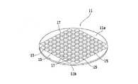
以下、本発明の実施形態を図面を参照して詳細に説明する。図1を参照すると、半導体ウェーハ(以下、単にウェーハと略称することがある)11の表面側斜視図が示されている。ウェーハ11は、図4に示すように、シリコンウェーハ等の基板12と、基板12上に形成された低誘電率絶縁膜(Low−k膜)を含む積層体13とから形成されている。 Hereinafter, embodiments of the present invention will be described in detail with reference to the drawings. Referring to FIG. 1, a front side perspective view of a semiconductor wafer 11 (hereinafter sometimes simply referred to as a wafer) 11 is shown. As shown in FIG. 4, the
ウェーハ11の表面11aに形成された積層体13には、格子状に形成された複数の分割予定ライン(ストリート)15によって区画された各領域にIC,LSI等のデバイス17が形成されている。ウェーハ11の厚みは、例えば100μm程度である。 In the laminated
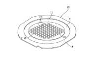
本発明のウェーハの加工方法では、図2に示すように、ウェーハ11の裏面11bを、外周部が環状フレームFに貼着された粘着テープであるダイシングテープTに貼着し、ウェーハユニット19を形成する。ウェーハユニット19では、ウェーハ11はダイシングテープTを介して環状フレームFで支持された状態となる。 In the wafer processing method of the present invention, as shown in FIG. 2, the
ウェーハユニット19を形成した後、ウェーハ11の分割予定ライン15に沿って切削ブレードで積層体13を切削し、切削溝を形成する切削溝形成ステップを実施する。この切削溝形成ステップでは、ウェーハ11の基板12に至らない深さの切削溝を形成する。 After the
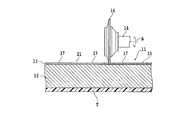
切削溝形成ステップは、図3に示す切削装置の切削ユニット10により実施する。切削ユニット10は、スピンドルハウジング12中に回転可能に収容されたスピンドル14の先端に切削ブレード16が着脱可能に装着されて構成されている。 The cutting groove forming step is performed by the
この切削溝形成ステップでは、切削装置のチャックテーブル18でダイシングテープTを介してウェーハ11を吸引保持し、切削ブレード16を矢印A方向に高速回転させながら、図4に示すように、積層体13と基板12との境界まで切り込ませつつ、チャックテーブル18を矢印X1方向に加工送りしながら、分割予定ライン15に沿って積層体13を切削して切削溝21を形成する。 In this cutting groove forming step, the
積層体13と基板12との境界まで切削ブレード16が切り込むのが好ましいが、ダイシングテープTの厚みばらつきや切り込み深さ制御の誤差を考慮して、基板12を切削しないように積層体13を数μm程度切り残して切削溝21を形成するのが好ましい。 It is preferable that the
切削ユニット10を分割予定ライン15のピッチずつ割り出し送りしながら、第1の方向に伸長する全ての分割予定ライン15に沿って同様な切削溝21を形成する。次いで、チャックテーブル18を90°回転してから、第1の方向と直交する第2の方向に伸長する全ての分割予定ライン15に沿って同様な切削溝21を形成する。 While the
本実施形態の切削溝形成ステップでは、ウェーハ11の基板12を切削しないため、細粒径の切削ブレード16を使用するのが好ましい。更に、厚み10μm以下の切削ブレード16で切削溝21を形成するため、Low−k膜が雲母のように剥がれる所謂デラミネーションの発生を防止することができる。加えて、細粒径の切削ブレード16を使用することにより、デラミネーションの発生を防止できる。 In the cutting groove forming step of the present embodiment, since the
切削溝形成ステップを実施した後、ウェーハ11の基板2に対して透過性を有する波長のレーザビームの集光点を基板12の内部に位置付けた状態で、レーザビームをウェーハ11の裏面11b側から分割予定ライン15に沿って照射して、基板12の内部に分割予定ライン15に沿った改質層を形成する改質層形成ステップを実施する。 After performing the cutting groove forming step, the laser beam is irradiated from the
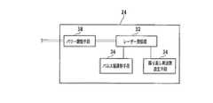
この改質層形成ステップを、図5乃至図7を参照して説明する。図5を参照すると、レーザビーム照射ユニット20は、実質上水平に配置された円筒形状のケーシング22を有している。 This modified layer forming step will be described with reference to FIGS. Referring to FIG. 5, the laser
ケーシング22内には、図6に示されたレーザビーム発生ユニット24が収容されており、ケーシング22の先端部には、レーザビーム発生ユニット24から発生されたレーザビームを集光する集光器26が装着されている。 A laser
レーザビーム発生ユニット24は、図6に示すように、YAGパルスレーザ発振器あるいはYVO4パルスレーザ発振器等のパルスレーザ発振器32と、繰り返し周波数設定手段34と、パルス幅調整手段36と、パワー調整手段38を含んでいる。 As shown in FIG. 6, the laser
レーザビーム発生ユニット20のケーシング22には撮像ユニット(撮像手段)28が装着されている。撮像ユニット28は、可視光線によって撮像するCCD等の通常の撮像素子の他に、ウェーハ11に赤外線を照射する赤外線照射手段と、赤外線に対応した電気信号を出力する赤外線CCD等の赤外線撮像素子を含んで構成されており、撮像した画像信号は図示しない制御手段に送信される。 An imaging unit (imaging means) 28 is attached to the
レーザ加工装置を用いてウェーハ11の基板12の内部に改質層を形成するには、図5に示すように、レーザ加工装置のチャックテーブル30上にダイシングテープTを上にしてウェーハ11の表面11a側を載置する。 In order to form a modified layer inside the
そして、図示しない吸引手段によってチャックテーブル30上にウェーハ11を吸引保持する。従って、チャックテーブル30上に吸引保持されたウェーハ11は裏面11bが上側となり、ダイシングテープTが上方に露出する。 Then, the
改質層形成ステップを実施する前に、撮像ユニット28によってウェーハ11のレーザ加工すべき加工領域を検出するアライメントを実施する。即ち、撮像ユニット28及び図示しない制御手段は、ウェーハ11の第1の方向に伸長する分割予定ライン15と、分割予定ライン15に沿ってレーザビームを照射するレーザビーム照射ユニット20の集光器26との位置合わせを行うためのパターンマッチング等の画像処理を実行し、レーザビーム照射位置のアライメントを遂行する。 Prior to performing the modified layer forming step, alignment for detecting a processing region of the
次いで、ウェーハ11に形成されている第1の方向に対して直交する第2の方向に伸長する分割予定ライン15に対しても、同様にレーザビーム照射位置のアライメントを遂行する。 Next, the alignment of the laser beam irradiation position is similarly performed on the
この時、ウェーハ11の分割予定ライン15が形成されている表面11aは下側に位置しているが、撮像ユニット28が赤外線撮像素子を備えているので、ダイシングテープT及びウェーハ11の裏面11b側から透かして分割予定ライン15を撮像することができる。 At this time, the
アライメント実施後、チャックテーブル30をレーザビームを照射するレーザビーム照射ユニット20の集光器26が位置するレーザビーム照射位置に移動し、第1の方向に伸長する分割予定ライン15の一端を集光器26の直下に位置付ける。 After the alignment, the chuck table 30 is moved to the laser beam irradiation position where the
そして、集光器26からダイシングテープT及びウェーハ11の基板12に対して透過性を有する波長のレーザビームの集光点を基板12の内部に位置付けた状態で、ウェーハ11の裏面側からパルスレーザビームを照射しつつ、チャックテーブル30を矢印X1方向に所定の送り速度で移動する。集光器26のレーザビーム照射位置が分割予定ライン15の他端に達したなら、パルスレーザビームの照射を停止するとともにチャックテーブル30の移動を停止する。 Then, with the condensing point of the laser beam having a wavelength transmissive to the dicing tape T and the
次いで、チャックテーブル30を分割予定ライン15のピッチだけ割り出し送りして、隣接する分割予定ライン15の他端に集光器26を位置付け、チャックテーブル30を矢印X2方向に所定の送り速度で加工送りしながら、隣接する分割予定ライン15に対応する基板12の内部に同様な改質層を形成する。 Next, the chuck table 30 is indexed and fed by the pitch of the scheduled
チャックテーブル30をX1方向及びX2方向に交互に加工送りしながら、第1の方向に伸長する分割予定ライン15に対応する基板2の内部に改質層23を形成する。第1の方向に伸長する全ての分割予定ライン15に沿って改質層23を形成したならば、チャックテーブル30を90°回転してから、第1の方向に直交する第2の方向に伸長する分割予定ライン15に沿って基板15の内部に同様な改質層23を形成する。 While the chuck table 30 is alternately processed and fed in the X1 direction and the X2 direction, the modified
改質層23は、密度、屈折率、機械的強度等の物理特性が周囲とは異なる状態になった領域をいい、溶融再硬化層として形成される。改質層23が基板2の内部に形成されると、改質層23から上下方向に伸びるマイクロクラックが形成される。 The modified
この改質層形成ステップにおける加工条件は、例えば次のように設定されている。 The processing conditions in this modified layer forming step are set as follows, for example.
光源 :LD励起Qスイッチ Nd:YVO4パルスレーザ
波長 :1064nm
繰り返し周波数 :100kHz
パルス出力 :10μJ
集光スポット径 :φ1μm
加工送り速度 :100mm/秒Light source: LD excitation Q switch Nd: YVO 4 pulse laser Wavelength: 1064 nm
Repetition frequency: 100 kHz
Pulse output: 10μJ
Condensing spot diameter: φ1μm
Processing feed rate: 100 mm / sec
改質層形成ステップ実施後、改質層23が形成されたウェーハ11に外力を付与して改質層23を分割起点にウェーハ11を分割予定ライン15に沿って個々のチップに分割する分割ステップを実施する。After performing the modified layer forming step, a dividing step of applying an external force to the
分割ステップでは、図8(A)に示すように、ウェーハ11をダイシングテープTを介して支持した環状フレームFを、フレーム保持部材46の載置面46a上に載置し、クランプ48によってフレーム保持部材46を固定する。この時、フレーム保持部材46はその載置面46aが拡張ドラム44の上端と略同一高さとなる基準位置に位置付けられる。 In the dividing step, as shown in FIG. 8A, the annular frame F that supports the
次いで、エアシリンダ52を駆動してフレーム保持部材46を図8(B)に示す拡張位置に下降する。これにより、フレーム保持部材46の載置面46a上に固定されている環状フレームFを下降するため、環状フレームFに貼着されたダイシングテープTは拡張ドラム44の上端縁に当接して主に半径方向に拡張される。 Next, the
その結果、ダイシングテープTに貼着されているウェーハ11には放射状に引っ張り力が作用する。このようにウェーハ11に放射状に引っ張り力が作用すると、図9に示すように、改質層23からのクラック27が切削溝21に向かってまっすぐ伸長し、ウェーハ11を改質層23を分割起点に分割予定ライン15に沿って個々のチップ25に分割することができる。 As a result, a tensile force acts radially on the
即ち、本実施形態では、基板2上に形成された積層体13に厚みの薄い切削ブレード16で切削溝21を形成するため、切削溝21の周囲が変質することがない。従って、ウェーハ11に外力を付与してウェーハ11を個々のチップに分割するときに、改質層23からクラック27が切削溝21に向かってまっすぐ伸長するため、従来方法のように分割不良が発生する恐れを低減することができる。 That is, in this embodiment, since the cutting
上述した実施形態では、ウェーハ11の積層体13に層間絶縁膜として低誘電率絶縁膜(Low−k膜)を含んでいるウェーハ11について説明したが、本発明のウェーハの加工方法は、層間絶縁膜としてSiO2絶縁膜を含むウェーハに対しても同様に適用することができる。In the above-described embodiment, the
11 半導体ウェーハ
12 基板
13 積層体
15 分割予定ライン
16 切削ブレード
17 デバイス
20 レーザビーム照射ユニット
21 切削溝
23 改質層
25 チップ
26 集光器
28 撮像ユニットDESCRIPTION OF
Claims (3)
Translated fromJapanese分割予定ラインに沿って切削ブレードで該積層体を切削して切削溝を形成する切削溝形成ステップと、
該切削溝形成ステップを実施した後、該基板に対して透過性を有する波長のレーザビームの集光点を該基板の内部に位置付けた状態で、該レーザビームをウェーハの裏面側から該分割予定ラインに沿って照射して、該基板の内部に該分割予定ラインに沿った改質層を形成する改質層形成ステップと、
該改質層形成ステップを実施した後、ウェーハに外力を付与してウェーハを該分割予定ラインに沿って個々のチップに分割する分割ステップと、
を備えたことを特徴とするウェーハの加工方法。Processing of a wafer comprising a substrate and a laminated body formed on the substrate, wherein a plurality of division lines intersecting in a lattice pattern by the laminated body and devices formed in each region partitioned by the division line A method,
A cutting groove forming step of cutting the laminated body with a cutting blade along a division schedule line to form a cutting groove;
After performing the cutting groove forming step, the laser beam is scheduled to be divided from the back side of the wafer with the condensing point of the laser beam having a wavelength transmissive to the substrate positioned inside the substrate. A modified layer forming step of irradiating along the line to form a modified layer along the line to be divided inside the substrate;
After performing the modified layer forming step, a dividing step of applying an external force to the wafer to divide the wafer into individual chips along the planned dividing line;
A wafer processing method characterized by comprising:
Priority Applications (3)
| Application Number | Priority Date | Filing Date | Title |
|---|---|---|---|
| JP2014085822AJP2015207604A (en) | 2014-04-17 | 2014-04-17 | Wafer processing method |
| US14/684,991US20150303113A1 (en) | 2014-04-17 | 2015-04-13 | Wafer processing method |
| CN201510173907.2ACN105047612B (en) | 2014-04-17 | 2015-04-13 | wafer processing method |
Applications Claiming Priority (1)
| Application Number | Priority Date | Filing Date | Title |
|---|---|---|---|
| JP2014085822AJP2015207604A (en) | 2014-04-17 | 2014-04-17 | Wafer processing method |
Publications (1)
| Publication Number | Publication Date |
|---|---|
| JP2015207604Atrue JP2015207604A (en) | 2015-11-19 |
Family
ID=54322628
Family Applications (1)
| Application Number | Title | Priority Date | Filing Date |
|---|---|---|---|
| JP2014085822APendingJP2015207604A (en) | 2014-04-17 | 2014-04-17 | Wafer processing method |
Country Status (3)
| Country | Link |
|---|---|
| US (1) | US20150303113A1 (en) |
| JP (1) | JP2015207604A (en) |
| CN (1) | CN105047612B (en) |
Cited By (4)
| Publication number | Priority date | Publication date | Assignee | Title |
|---|---|---|---|---|
| JP2016111293A (en)* | 2014-12-10 | 2016-06-20 | 株式会社東京精密 | Wafer dividing method and wafer dividing apparatus |
| KR20190120701A (en)* | 2018-04-16 | 2019-10-24 | 가부시기가이샤 디스코 | Processing method of a wafer |
| KR20200056915A (en)* | 2018-11-15 | 2020-05-25 | 가부시기가이샤 디스코 | Processing method of a laminate |
| CN111199916A (en)* | 2018-11-16 | 2020-05-26 | 株式会社迪思科 | Method for processing laminate |
Families Citing this family (11)
| Publication number | Priority date | Publication date | Assignee | Title |
|---|---|---|---|---|
| JP6651257B2 (en)* | 2016-06-03 | 2020-02-19 | 株式会社ディスコ | Workpiece inspection method, inspection device, laser processing device, and expansion device |
| JP6779574B2 (en)* | 2016-12-14 | 2020-11-04 | 株式会社ディスコ | Interposer manufacturing method |
| JP6817822B2 (en)* | 2017-01-18 | 2021-01-20 | 株式会社ディスコ | Processing method |
| JP6802085B2 (en)* | 2017-02-21 | 2020-12-16 | 株式会社ディスコ | Wafer processing method |
| JP2018181901A (en)* | 2017-04-04 | 2018-11-15 | 株式会社ディスコ | Processing method |
| JP6821261B2 (en)* | 2017-04-21 | 2021-01-27 | 株式会社ディスコ | Processing method of work piece |
| JP7139037B2 (en)* | 2018-05-11 | 2022-09-20 | 株式会社ディスコ | Chip manufacturing method |
| US20190363017A1 (en)* | 2018-05-24 | 2019-11-28 | Semiconductor Components Industries, Llc | Die sawing singulation systems and methods |
| JP7460274B2 (en)* | 2020-02-21 | 2024-04-02 | 株式会社ディスコ | Wafer processing method |
| KR102152007B1 (en)* | 2020-03-18 | 2020-09-04 | 주식회사 탑 엔지니어링 | Method and apparatus for cutting substrate |
| CN115770960B (en)* | 2021-11-25 | 2025-01-07 | 湖南大学 | Composite cutting process of semiconductor material containing back gold layer |
Citations (3)
| Publication number | Priority date | Publication date | Assignee | Title |
|---|---|---|---|---|
| JP2005012203A (en)* | 2003-05-29 | 2005-01-13 | Hamamatsu Photonics Kk | Laser machining method |
| JP2012199374A (en)* | 2011-03-22 | 2012-10-18 | Fujitsu Semiconductor Ltd | Method of manufacturing semiconductor chip |
| JP2013080972A (en)* | 2005-11-10 | 2013-05-02 | Renesas Electronics Corp | Method of manufacturing semiconductor device |
Family Cites Families (5)
| Publication number | Priority date | Publication date | Assignee | Title |
|---|---|---|---|---|
| US20020001876A1 (en)* | 1999-01-26 | 2002-01-03 | Mahjoub Ali Abdelgadir | Method of making an integrated circuit device having a planar interlevel dielectric layer |
| US6467138B1 (en)* | 2000-05-24 | 2002-10-22 | Vermon | Integrated connector backings for matrix array transducers, matrix array transducers employing such backings and methods of making the same |
| EP1575081A1 (en)* | 2002-10-28 | 2005-09-14 | Tokyo Seimitsu Co.,Ltd. | Expansion method and device |
| JP2004146727A (en)* | 2002-10-28 | 2004-05-20 | Tokyo Seimitsu Co Ltd | Transferring method of wafer |
| WO2007055010A1 (en)* | 2005-11-10 | 2007-05-18 | Renesas Technology Corp. | Semiconductor device manufacturing method and semiconductor device |
- 2014
- 2014-04-17JPJP2014085822Apatent/JP2015207604A/enactivePending
- 2015
- 2015-04-13USUS14/684,991patent/US20150303113A1/ennot_activeAbandoned
- 2015-04-13CNCN201510173907.2Apatent/CN105047612B/enactiveActive
Patent Citations (3)
| Publication number | Priority date | Publication date | Assignee | Title |
|---|---|---|---|---|
| JP2005012203A (en)* | 2003-05-29 | 2005-01-13 | Hamamatsu Photonics Kk | Laser machining method |
| JP2013080972A (en)* | 2005-11-10 | 2013-05-02 | Renesas Electronics Corp | Method of manufacturing semiconductor device |
| JP2012199374A (en)* | 2011-03-22 | 2012-10-18 | Fujitsu Semiconductor Ltd | Method of manufacturing semiconductor chip |
Cited By (13)
| Publication number | Priority date | Publication date | Assignee | Title |
|---|---|---|---|---|
| JP2016111293A (en)* | 2014-12-10 | 2016-06-20 | 株式会社東京精密 | Wafer dividing method and wafer dividing apparatus |
| KR20190120701A (en)* | 2018-04-16 | 2019-10-24 | 가부시기가이샤 디스코 | Processing method of a wafer |
| KR102629098B1 (en) | 2018-04-16 | 2024-01-24 | 가부시기가이샤 디스코 | Processing method of a wafer |
| JP7164411B2 (en) | 2018-11-15 | 2022-11-01 | 株式会社ディスコ | Laminate processing method |
| KR20200056915A (en)* | 2018-11-15 | 2020-05-25 | 가부시기가이샤 디스코 | Processing method of a laminate |
| KR102713532B1 (en) | 2018-11-15 | 2024-10-04 | 가부시기가이샤 디스코 | Processing method of a laminate |
| JP2020087973A (en)* | 2018-11-15 | 2020-06-04 | 株式会社ディスコ | Processing method of laminated body |
| CN111199916A (en)* | 2018-11-16 | 2020-05-26 | 株式会社迪思科 | Method for processing laminate |
| JP7164412B2 (en) | 2018-11-16 | 2022-11-01 | 株式会社ディスコ | Laminate processing method |
| CN111199916B (en)* | 2018-11-16 | 2023-08-01 | 株式会社迪思科 | Processing method of laminated body |
| JP2020088002A (en)* | 2018-11-16 | 2020-06-04 | 株式会社ディスコ | Processing method of laminated body |
| KR20200057624A (en)* | 2018-11-16 | 2020-05-26 | 가부시기가이샤 디스코 | Processing method of a laminate |
| KR102721280B1 (en) | 2018-11-16 | 2024-10-23 | 가부시기가이샤 디스코 | Processing method of a laminate |
Also Published As
| Publication number | Publication date |
|---|---|
| CN105047612A (en) | 2015-11-11 |
| US20150303113A1 (en) | 2015-10-22 |
| CN105047612B (en) | 2020-02-21 |
Similar Documents
| Publication | Publication Date | Title |
|---|---|---|
| JP2015207604A (en) | Wafer processing method | |
| JP4959422B2 (en) | Wafer division method | |
| JP4694845B2 (en) | Wafer division method | |
| JP6078376B2 (en) | Wafer processing method | |
| JP4422463B2 (en) | Semiconductor wafer dividing method | |
| JP6178077B2 (en) | Wafer processing method | |
| JP5608521B2 (en) | Semiconductor wafer dividing method, semiconductor chip and semiconductor device | |
| JP2009021476A (en) | Wafer division method | |
| JP2015213135A (en) | Wafer processing method | |
| KR102349663B1 (en) | Wafer processing method | |
| JP2011187479A (en) | Wafer processing method | |
| JP6189208B2 (en) | Wafer processing method | |
| JP5992731B2 (en) | Wafer processing method | |
| KR20190008103A (en) | Method for manufacturing a glass interposer | |
| JP2008283025A (en) | Wafer division method | |
| JP6246534B2 (en) | Wafer processing method | |
| JP2016018881A (en) | Wafer processing method | |
| JP2007173475A (en) | Wafer division method | |
| JP2008028113A (en) | Wafer laser processing method | |
| JP2006032419A (en) | Wafer laser processing method | |
| CN108022877A (en) | The processing method of chip | |
| KR101893617B1 (en) | Manufacturing method of chip | |
| TW201935549A (en) | Wafer processing method which does not change the control system of the laser processing device to smoothly divide a wafer configured with bumps | |
| JP2018098378A (en) | Manufacturing method of interposer | |
| JP6558973B2 (en) | Device chip manufacturing method |
Legal Events
| Date | Code | Title | Description |
|---|---|---|---|
| A621 | Written request for application examination | Free format text:JAPANESE INTERMEDIATE CODE: A621 Effective date:20170216 | |
| A977 | Report on retrieval | Free format text:JAPANESE INTERMEDIATE CODE: A971007 Effective date:20171018 | |
| A131 | Notification of reasons for refusal | Free format text:JAPANESE INTERMEDIATE CODE: A131 Effective date:20171114 | |
| A02 | Decision of refusal | Free format text:JAPANESE INTERMEDIATE CODE: A02 Effective date:20180703 |